WO2014208288A1 - プラズマ処理装置及びプラズマ処理方法 - Google Patents
プラズマ処理装置及びプラズマ処理方法 Download PDFInfo
- Publication number
- WO2014208288A1 WO2014208288A1 PCT/JP2014/064680 JP2014064680W WO2014208288A1 WO 2014208288 A1 WO2014208288 A1 WO 2014208288A1 JP 2014064680 W JP2014064680 W JP 2014064680W WO 2014208288 A1 WO2014208288 A1 WO 2014208288A1
- Authority
- WO
- WIPO (PCT)
- Prior art keywords
- plasma processing
- cathode electrode
- upper electrode
- processing apparatus
- frequency power
- Prior art date
- Legal status (The legal status is an assumption and is not a legal conclusion. Google has not performed a legal analysis and makes no representation as to the accuracy of the status listed.)
- Ceased
Links
Images







Classifications
-
- C—CHEMISTRY; METALLURGY
- C23—COATING METALLIC MATERIAL; COATING MATERIAL WITH METALLIC MATERIAL; CHEMICAL SURFACE TREATMENT; DIFFUSION TREATMENT OF METALLIC MATERIAL; COATING BY VACUUM EVAPORATION, BY SPUTTERING, BY ION IMPLANTATION OR BY CHEMICAL VAPOUR DEPOSITION, IN GENERAL; INHIBITING CORROSION OF METALLIC MATERIAL OR INCRUSTATION IN GENERAL
- C23C—COATING METALLIC MATERIAL; COATING MATERIAL WITH METALLIC MATERIAL; SURFACE TREATMENT OF METALLIC MATERIAL BY DIFFUSION INTO THE SURFACE, BY CHEMICAL CONVERSION OR SUBSTITUTION; COATING BY VACUUM EVAPORATION, BY SPUTTERING, BY ION IMPLANTATION OR BY CHEMICAL VAPOUR DEPOSITION, IN GENERAL
- C23C16/00—Chemical coating by decomposition of gaseous compounds, without leaving reaction products of surface material in the coating, i.e. chemical vapour deposition [CVD] processes
- C23C16/44—Chemical coating by decomposition of gaseous compounds, without leaving reaction products of surface material in the coating, i.e. chemical vapour deposition [CVD] processes characterised by the method of coating
- C23C16/50—Chemical coating by decomposition of gaseous compounds, without leaving reaction products of surface material in the coating, i.e. chemical vapour deposition [CVD] processes characterised by the method of coating using electric discharges
- C23C16/505—Chemical coating by decomposition of gaseous compounds, without leaving reaction products of surface material in the coating, i.e. chemical vapour deposition [CVD] processes characterised by the method of coating using electric discharges using radio frequency discharges
- C23C16/509—Chemical coating by decomposition of gaseous compounds, without leaving reaction products of surface material in the coating, i.e. chemical vapour deposition [CVD] processes characterised by the method of coating using electric discharges using radio frequency discharges using internal electrodes
-
- H—ELECTRICITY
- H01—ELECTRIC ELEMENTS
- H01J—ELECTRIC DISCHARGE TUBES OR DISCHARGE LAMPS
- H01J37/00—Discharge tubes with provision for introducing objects or material to be exposed to the discharge, e.g. for the purpose of examination or processing thereof
- H01J37/32—Gas-filled discharge tubes
- H01J37/32009—Arrangements for generation of plasma specially adapted for examination or treatment of objects, e.g. plasma sources
- H01J37/32082—Radio frequency generated discharge
- H01J37/32091—Radio frequency generated discharge the radio frequency energy being capacitively coupled to the plasma
-
- H—ELECTRICITY
- H01—ELECTRIC ELEMENTS
- H01J—ELECTRIC DISCHARGE TUBES OR DISCHARGE LAMPS
- H01J37/00—Discharge tubes with provision for introducing objects or material to be exposed to the discharge, e.g. for the purpose of examination or processing thereof
- H01J37/32—Gas-filled discharge tubes
- H01J37/32009—Arrangements for generation of plasma specially adapted for examination or treatment of objects, e.g. plasma sources
- H01J37/32082—Radio frequency generated discharge
- H01J37/32174—Circuits specially adapted for controlling the RF discharge
- H01J37/32183—Matching circuits
-
- H—ELECTRICITY
- H01—ELECTRIC ELEMENTS
- H01J—ELECTRIC DISCHARGE TUBES OR DISCHARGE LAMPS
- H01J37/00—Discharge tubes with provision for introducing objects or material to be exposed to the discharge, e.g. for the purpose of examination or processing thereof
- H01J37/32—Gas-filled discharge tubes
- H01J37/32431—Constructional details of the reactor
- H01J37/32532—Electrodes
- H01J37/32541—Shape
-
- H—ELECTRICITY
- H01—ELECTRIC ELEMENTS
- H01J—ELECTRIC DISCHARGE TUBES OR DISCHARGE LAMPS
- H01J37/00—Discharge tubes with provision for introducing objects or material to be exposed to the discharge, e.g. for the purpose of examination or processing thereof
- H01J37/32—Gas-filled discharge tubes
- H01J37/32431—Constructional details of the reactor
- H01J37/32532—Electrodes
- H01J37/32577—Electrical connecting means
-
- H—ELECTRICITY
- H01—ELECTRIC ELEMENTS
- H01J—ELECTRIC DISCHARGE TUBES OR DISCHARGE LAMPS
- H01J37/00—Discharge tubes with provision for introducing objects or material to be exposed to the discharge, e.g. for the purpose of examination or processing thereof
- H01J37/32—Gas-filled discharge tubes
- H01J37/32431—Constructional details of the reactor
- H01J37/32733—Means for moving the material to be treated
- H01J37/32752—Means for moving the material to be treated for moving the material across the discharge
- H01J37/32761—Continuous moving
- H01J37/32779—Continuous moving of batches of workpieces
-
- H—ELECTRICITY
- H05—ELECTRIC TECHNIQUES NOT OTHERWISE PROVIDED FOR
- H05H—PLASMA TECHNIQUE; PRODUCTION OF ACCELERATED ELECTRICALLY-CHARGED PARTICLES OR OF NEUTRONS; PRODUCTION OR ACCELERATION OF NEUTRAL MOLECULAR OR ATOMIC BEAMS
- H05H1/00—Generating plasma; Handling plasma
- H05H1/24—Generating plasma
- H05H1/46—Generating plasma using applied electromagnetic fields, e.g. high frequency or microwave energy
-
- H—ELECTRICITY
- H05—ELECTRIC TECHNIQUES NOT OTHERWISE PROVIDED FOR
- H05H—PLASMA TECHNIQUE; PRODUCTION OF ACCELERATED ELECTRICALLY-CHARGED PARTICLES OR OF NEUTRONS; PRODUCTION OR ACCELERATION OF NEUTRAL MOLECULAR OR ATOMIC BEAMS
- H05H2242/00—Auxiliary systems
- H05H2242/20—Power circuits
- H05H2242/26—Matching networks
Definitions
- the present invention relates to a plasma processing apparatus and a plasma processing method for performing plasma processing on an object to be processed.
- a predetermined process such as etching or film formation is performed on a large substrate.
- a plasma processing apparatus used for such processing a parallel plate type plasma processing apparatus is known.
- Patent Document 1 Japanese Patent Laid-Open No. 11-243062
- a feeding point for a long plate-like or rod-like electrode is used.
- a plasma CVD apparatus has been proposed in which a phase adjustment circuit for adjusting the phase of reflected wave power is connected to the opposite side.
- Patent Document 1 a plurality of long high-frequency electrodes are arranged on a single substrate to achieve uniform processing within the substrate surface.
- a batch type parallel plate type plasma processing apparatus in which parallel plate electrodes are stacked in multiple stages has been studied.
- a plurality of sets of parallel plate electrodes must be stacked and arranged in a processing container, so that the position of feeding high-frequency power to the cathode is restricted.
- a power feeding part is provided unevenly on one side of the cathode. Therefore, it is difficult to uniformly supply high-frequency power at the cathode, and there is a problem that it is difficult to ensure the uniformity of processing within the surface of a large substrate as compared with a single wafer plasma processing apparatus.
- the present invention provides a plasma processing apparatus capable of ensuring the uniformity of processing within the substrate surface.
- the plasma processing apparatus of the present invention includes a processing container that can be evacuated, and a cathode electrode and an anode electrode that are disposed to face each other with the substrate interposed therebetween in the processing container.
- the plasma processing apparatus of the present invention includes a first high-frequency power source that supplies high-frequency power to the cathode electrode, and one or a plurality of impedance adjustment devices that are connected to the cathode electrode and adjust the impedance of the cathode electrode. It is equipped with.
- the cathode electrode in the cathode electrode, at least one connection part among the power supply part to which the high-frequency power is supplied and the connection part to which the impedance adjusting device is connected is the cathode electrode. They are formed on opposite sides of the surface facing the anode electrode.
- one cathode processing electrode and one anode electrode may be paired to form one plasma processing unit, and a plurality of the plasma processing units are provided in the processing container. It may be arranged in a stacked manner.
- the cathode electrode may have a square shape in plan view, and the power feeding portion may be provided on a side portion of the cathode electrode forming one side of the square shape.
- the connection portions may be provided on a side portion of the cathode electrode that forms one side opposite to one side of the square.
- a plurality of the impedance adjusting devices may be connected to one cathode electrode.
- the cathode electrode may have a square shape in plan view, and the power feeding portion may be provided on a side portion of the cathode electrode forming one side of the square shape.
- the connection part may be provided at a plurality of locations on the side of the cathode electrode forming one side opposite to one side of the quadrangle. In this case, at least two of the connection parts may be provided at symmetrical positions so that the distances from the power feeding part are equal.
- the plasma processing apparatus of the present invention may further include a second high frequency power source for supplying high frequency power to the cathode electrode via the impedance adjusting device.
- the impedance adjusting device may include a combination of an inductive element and a capacitive element.
- the inductive element may be a variable inductive element.
- the capacitive element may be a variable capacitive element.
- a substrate is disposed between the cathode electrode and the anode electrode to perform plasma processing.
- the cathode electrode includes a feeding portion to which high-frequency power is supplied and a connection portion to which an impedance adjusting device for adjusting the impedance of the cathode electrode is connected. Were formed on opposite sides of each other. Thereby, according to the plasma processing apparatus of the present invention, even when processing a large substrate having a large area, for example, it is possible to ensure processing uniformity within the substrate surface.
- FIG. 1 is a sectional view showing a schematic configuration example of a plasma processing apparatus according to a first embodiment of the present invention.
- a plasma processing apparatus 100 includes a processing container 1 that can be evacuated to accommodate a rectangular substrate S that is an object to be processed, and cathode electrodes that are disposed to face each other in the processing container 1.
- the upper electrode 3 and the lower electrode 5 as an anode electrode are provided.
- the plasma processing apparatus 100 includes a high frequency power source 7 as a first high frequency power source for supplying high frequency power to the upper electrode 3, and an impedance adjusting device 9 that is connected to the upper electrode 3 and adjusts the impedance of the upper electrode 3.
- the plasma processing apparatus 100 is configured as a batch type parallel plate type plasma processing apparatus that performs film formation, etching, and the like on a plurality of substrates S simultaneously.
- the substrate S include an FPD glass substrate and a solar cell substrate.
- the FPD include a liquid crystal display (LCD), an electroluminescence (EL) display, a plasma display panel (PDP), and the like.
- the plasma processing apparatus 100 of the present embodiment is suitable for processing a large substrate S having a short side exceeding 1 m, for example.
- the processing container 1 has a box shape that can be evacuated.
- the processing container 1 is grounded.
- a metal such as aluminum, an aluminum alloy, or stainless steel is used for the processing container 1.
- the processing container 1 includes a ceiling portion 11, a rectangular tubular side wall portion 13, and a bottom wall portion 15.
- the side wall 13 is provided with an opening (not shown) that is opened and closed when the substrate S is loaded and unloaded, and the opening is opened and closed by a gate valve.
- an exhaust port 15 a is formed in the bottom wall portion 15.
- the exhaust port 15 a is connected to the exhaust device 21 via the exhaust pipe 23.
- the exhaust port is not limited to the bottom wall portion 15 and may be provided in the ceiling portion 11, for example.
- the upper electrode 3 and the lower electrode 5 are arranged in parallel to each other and form a pair of parallel plate electrodes. Both the upper electrode 3 and the lower electrode 5 are made of a metal such as aluminum, aluminum alloy, stainless steel, or the like.
- the upper electrode 3 has a function as a shower head for introducing gas into the processing container 1. That is, the upper electrode 3 has a hollow shape, and a gas diffusion space 31 is provided therein. A plurality of gas discharge holes 33 for discharging a processing gas are formed on the lower surface of the upper electrode 3. Further, a gas introduction portion 35 communicating with the gas diffusion space 31 is provided on the side portion of the upper electrode 3. Further, the lower surface of the upper electrode 3 forms a facing surface 37 facing the lower electrode 5.
- the upper electrode 3 may not have a function as a shower head.
- the upper electrode 3 may be a flat metal plate that does not include the gas diffusion space 31 and the gas discharge hole 33.
- the lower electrode 5 is fixed to the side wall 13 of the processing container 1 by an insulating member or a conductive member (both not shown). When it is fixed by an insulating member, conduction between the lower electrode 5 and the side wall portion 13 may be achieved by a conductive member. Therefore, the lower electrode 5 is at ground potential.
- the conductive portion 5 a indicates that the lower electrode 5 and the side wall portion 13 are in a conductive state.
- the upper surface of the lower electrode 5, that is, the surface facing the upper electrode 3 is a substrate placement surface on which the substrate S is placed.
- the lower electrode 5 has a plurality of substrate support pins (not shown) that can project and retract with respect to the substrate mounting surface, and use the substrate support pins to connect with an external transfer device. The delivery of the substrate S can be performed.
- one upper electrode 3 and one lower electrode 5 form a pair to constitute one plasma processing unit 10.
- a plurality of plasma processing units 10 are stacked in multiple stages.
- the plasma processing apparatus 100 can batch process a plurality of substrates S simultaneously.
- the number of plasma processing units 10 in the processing container 1 can be in the range of 3 to 20, for example.
- a feeding line 71 is connected to the upper electrode 3.
- the power supply line 71 is connected to a high-frequency power source 7 for plasma formation via a matching unit 73.
- high frequency power of 13.56 MHz, for example, is supplied from the high frequency power supply 7 to the upper electrode 3.
- the power supply line 71 is introduced into the processing container 1 through a power supply opening 13 a formed in the side wall portion 13 of the processing container 1.
- a vacuum holding means such as a bellows (not shown) is provided around the power supply opening 13a.
- the frequency of the high frequency power may be, for example, 11 MHz, 27.12 MHz, 40.68 MHz, 60 MHz, or the like.
- the matching unit 73 is provided with a matching circuit (not shown) having one end connected to the high frequency power supply 7 via a coaxial cable, for example, and the other end of the matching circuit is connected to the upper electrode via the feeder 71. 3 is connected.
- the matching circuit performs impedance adjustment (matching) between the load (plasma) and the high-frequency power source 7 in accordance with the impedance of the plasma, and plays a role of attenuating the reflected wave generated in the circuit of the plasma processing apparatus 100.
- the plasma processing apparatus 100 includes an impedance adjusting device 9 that adjusts the impedance of the upper electrode 3 for each upper electrode 3.
- An impedance adjusting device 9 is connected to each upper electrode 3 via a wiring 91.
- the impedance adjusting device 9 is grounded.
- the grounding of the impedance adjusting device 9 is not indispensable, and may be electrically connected to the lower electrode 5 serving as an anode electrode.
- the impedance adjusting device 9 is also grounded.
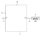
- FIG. 2 is an explanatory diagram showing a connection state between the upper electrode 3 and the impedance adjusting device 9.
- FIG. 2 together with a plan view of the upper electrode 3, a feeding part P ⁇ b> 1 where the feeding line 71 is connected to the upper electrode 3, and a connecting part P ⁇ b> 2 where the impedance adjusting device 9 is connected to the upper electrode 3 via the wiring 91. Show.
- the upper electrode 3 has a square shape, for example, a rectangular shape having a long side 3a and a short side 3b.
- a power feeding part P ⁇ b> 1 to which high frequency power is supplied from the high frequency power supply 7 via the power feeding line 71 and a connection part P ⁇ b> 2 to which the impedance adjusting device 9 is connected via the wiring 91 are a lower part in the upper electrode 3. They are formed on opposite sides of the electrode 5 facing the surface 37 (see FIG. 1).
- the power feeding part P1 and the connection part P2 are both provided on the side of the long side 3a of the upper electrode 3.
- the power feeding part P1 and the connection part P2 are provided in the vicinity of the midpoint that divides the long side 3a of the upper electrode 3 into two equal parts.
- the impedance adjusting device 9 can include a combination of an inductive element and a capacitive element.
- the inductive element for example, a loop coil, a solenoid coil, a linear wire, or the like can be used.
- a linear wire material that is not a loop shape functions as a dielectric element.
- a vacuum capacitor, a ceramic capacitor, or the like can be used as the capacitive element.
- the inductive element may be a fixed inductive element or a variable inductive element.
- the capacitive element may be a fixed capacitive element or a variable capacitive element.
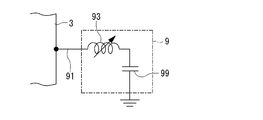
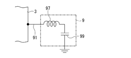
- 3A to 3D illustrate a preferable combination of the inductive element and the capacitive element in the impedance adjusting device 9.
- FIG. 3A shows a circuit in which a variable coil 93 that can change inductance and a variable capacitor 95 that can change capacitance are connected in series as the impedance adjusting device 9.
- FIG. 3B is a circuit in which a fixed coil 97 and a variable capacitor 95 capable of changing the capacitance are connected in series as the impedance adjusting device 9.
- FIG. 3C shows a circuit in which a variable coil 93 capable of changing the inductance and a fixed capacitor 99 are connected in series as the impedance adjusting device 9.
- FIG. 3D shows a circuit in which a fixed coil 97 and a fixed capacitor 99 are connected in series as the impedance adjusting device 9.
- the inductance in the variable coil 93 and the capacitance in the variable capacitor 95 can be adjusted by using a driving means such as a stepping motor, and can be controlled by the control unit 60. Further, for example, a dial or the like may be provided in the variable coil 93 or the variable capacitor 95 so that the inductance and capacitance can be manually adjusted.
- a series connection circuit of an inductive element and a capacitive element is provided as the impedance adjusting device 9 between the upper electrode 3 and the ground.
- the impedance adjusting device 9 is not limited to the circuit configuration illustrated above as long as it has a function of adjusting the impedance of the upper electrode 3.
- the impedance adjusting device 9 may be configured to include only one of the inductive element and the capacitive element as long as the impedance can be appropriately adjusted.
- the connection order of the inductive element and the capacitive element can be switched and connected.
- another inductive element or capacitive element may be further connected in series to the combination of the inductive element and the capacitive element shown in FIGS. 3A to 3D connected in series, or May be connected in parallel.
- the impedance adjusting device 9 of the present embodiment is connected in parallel to the parallel plate capacitance component by the upper electrode 3 and the lower electrode 5 and the plasma capacitance component. What is necessary is just to select the inductive element and capacitive element which can be used in the area
- the plasma processing apparatus 100 further includes an exhaust mechanism 20 that exhausts the inside of the processing container 1 under reduced pressure.
- the exhaust mechanism 20 includes, for example, an exhaust device 21 having a vacuum pump such as a dry pump, and an exhaust pipe 23 connecting the exhaust device 21 and the exhaust port 15a. By operating the vacuum pump of the exhaust device 21, the internal space of the processing container 1 is evacuated to a predetermined degree of vacuum.
- the plasma processing apparatus 100 further includes a gas supply device 40 that supplies gas into the processing container 1.
- the gas supply device 40 is connected to the gas supply source 41, a plurality of pipes 43 (only one is shown) for introducing a processing gas into the processing container 1, and a plurality of pipes 43 provided to these pipes 43.
- Valve 45 (only two are shown) and a mass flow controller (MFC) 47.
- the plurality of pipes 43 are connected to a gas introduction part 35 provided on a side part of the upper electrode 3 via a gas introduction part 13 b of the side wall part 13 of the processing container 1. Accordingly, the processing gas can be supplied from the gas supply source 41 to the gas diffusion space 31 via the pipe 43, the gas introduction part 13 b, and the gas introduction part 35.
- the type of gas supplied to the gas diffusion space 31 and the flow rate of these gases are controlled by opening and closing the mass flow controller 47 and the valve 45.
- an external gas supply device that is not included in the configuration of the plasma processing apparatus 100 may be used.
- the control unit 60 is typically a computer.
- the control unit 60 includes a controller 61 having a CPU, and a user interface 62 and a storage unit 63 connected to the controller 61.
- the controller 61 is configured by each component (for example, for example, high-frequency output, impedance matching by the matching unit 73, impedance adjustment of the upper electrode 3, pressure in the processing container 1, process conditions such as gas flow rate (for example, The high-frequency power source 7, the matching unit 73, the impedance adjustment device 9, the exhaust device 21, the gas supply device 40, etc.)
- component for example, for example, high-frequency output, impedance matching by the matching unit 73, impedance adjustment of the upper electrode 3, pressure in the processing container 1, process conditions such as gas flow rate (for example, The high-frequency power source 7, the matching unit 73, the impedance adjustment device 9, the exhaust device 21, the gas supply device 40, etc.)
- the user interface 62 includes a keyboard and a touch panel on which a process manager manages commands to manage the plasma processing apparatus 100, a display for visualizing and displaying the operating status of the plasma processing apparatus 100, and the like.
- the storage unit 63 stores a control program (software) for realizing various processes executed by the plasma processing apparatus 100 under the control of the controller 61, a recipe in which process condition data and the like are recorded.
- the controller 61 calls and executes an arbitrary control program or recipe from the storage unit 63 as necessary, such as an instruction from the user interface 62. Thus, a desired process is performed in the processing container 1 of the plasma processing apparatus 100 under the control of the controller 61.
- control program and recipe described above can be stored in a computer-readable storage medium such as a CD-ROM, hard disk, flexible disk, flash memory, or DVD. Also, the above recipe can be transmitted from other devices as needed via, for example, a dedicated line and used online.
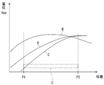
- FIG. 4 is a characteristic diagram showing the relationship between the magnitude of Vpp in the plane of the upper electrode 3 and the distance from the power feeding site P1.
- Vpp means the maximum value and the minimum value (peak value to peak) of the voltage of the high frequency power supplied from the high frequency power supply 7 to the upper electrode 3.
- the vertical axis of FIG. 4 indicates the magnitude of Vpp
- the horizontal axis indicates the distance from the power supply site P1 in the short side direction of the upper electrode 3 with reference to the power supply site P1 to which the high frequency power is supplied from the high frequency power source 7. Yes.
- the distance between P1 and P2 corresponds to the length of the short side 3b of the upper electrode 3 (see FIG. 2). ).
- size of the upper electrode 3 was shown with the dashed-two dotted line.
- the side where the power feeding part P1 is provided is the “P1 side”, and the open end or the connection part P2 of the impedance adjusting device 9 is provided. The side is denoted as “P2 side”.
- the distribution of Vpp in the cathode surface is such that Vpp increases from the power supply side (P1 side) toward the open end side (P2 side) in the short side direction of the cathode as shown by curve A in FIG. Distribution.
- Vpp has a distribution as shown by the curve A in FIG. 4
- the plasma density on the power supply side (P1 side) is smaller between the parallel plate electrodes than on the open end side (P2 side).
- Side showed a tendency to decrease the processing efficiency.
- “processing efficiency” means, for example, a deposition rate or crystallinity in the case of film formation by plasma CVD, and an etching rate in the case of plasma etching.
- the impedance adjusting device 9 is connected to the connection portion P2 on the opposite side of the power supply portion P1 in the upper electrode 3 and grounded.
- the impedance adjusting device 9 for example, by using a variable element having a combination of a variable inductance and a variable capacitance shown in FIG. 3A, the impedance on the side opposite to the power feeding part P1 (P2 side) can be finely adjusted. It becomes possible.
- the impedance adjustment device 9 adjusts the impedance on the opposite side (P2 side) to the feeding part P1 to the inductive impedance, thereby creating the distribution of Vpp as shown by the curve B in FIG. It becomes possible.
- the curve B has a smaller variation in Vpp than the curve A, and the Vpp distribution in the short side direction of the upper electrode 3 is equalized. Therefore, if a Vpp distribution like the curve B can be created, the plasma density can be made uniform between the parallel plate electrodes, and an even treatment can be performed in the plane of the substrate S.
- the impedance adjustment device 9 may adjust the capacitive impedance so as to increase.
- inductive impedance means that the combined impedance of the inductive element and the capacitive element is biased inductively.
- Capacitive impedance means that the combined impedance of the inductive element and the capacitive element is biased toward capacitive.
- the maximum value of Vpp tends to move toward the power feeding side (P1 side)
- the capacitive impedance becomes stronger the maximum value of Vpp becomes the opposite side to the feeding part P1. The tendency to move to (P2 side) is shown.
- the impedance adjustment device 9 can adjust the impedance of the upper electrode 3 to control the Vpp distribution in the electrode. Thereby, the density distribution of the plasma generated between the parallel plate electrodes can be adjusted.
- the feeding part P1 to the upper electrode 3 is restricted to the side part that is biased with respect to the opposed surface 37 to the lower electrode 5 in FIG.
- the impedance adjustment device 9 enables uniform processing within the surface of the substrate S.
- the impedance adjusting device 9 can also be used as a filter circuit by changing the constants of the inductive element and / or the capacitive element. In that case, since the effect which removes the harmonic component which generate
- the impedance adjusting device 9 can be realized by combining the inductive element and the capacitive element shown in FIGS. 3B to 3D, or other combinations. In the short side direction, impedance adjustment similar to the curves B and C in FIG. 4 is possible.
- a processing procedure when the plasma processing apparatus 100 performs a film forming process on the substrate S by the plasma CVD method will be described.
- a command is input from the user interface 62 to the controller 61 so as to perform a film forming process in the plasma processing apparatus 100.
- the controller 61 reads a recipe stored in the storage unit 63 or a computer-readable storage medium.
- each end device of the plasma processing apparatus 100 for example, the high-frequency power source 7, the matching unit 73, the impedance adjusting device 9, the exhaust device 21, the gas is processed so that the film forming process is executed according to the conditions based on the recipe.
- a control signal is sent to the supply device 40 and the like.
- the gate valve (not shown) is opened, and a plurality of substrates S are carried into the processing container 1 through the gate valve and the opening (not shown) of the side wall 13 by an external transfer device.
- the Each substrate S is placed on the lower electrode 5 via a plurality of substrate support pins (not shown).
- the gate valve is closed, and the inside of the processing container 1 is evacuated by the exhaust device 21.
- a processing gas having a predetermined flow rate is injected from the gas discharge hole 33 of the upper electrode 3 toward the upper surface of the substrate S by the gas supply device 40.
- the internal space of the processing container 1 is adjusted to a predetermined pressure by adjusting the exhaust amount and the gas supply amount.
- each upper electrode 3 by supplying high frequency power from the high frequency power supply 7 to each upper electrode 3, plasma of a processing gas is generated between the upper electrode 3 and the lower electrode 5 forming parallel plate electrodes in each plasma processing unit 10. Is done. A predetermined thin film is deposited on the surface of the substrate S by the generated plasma.
- the impedance adjustment device 9 adjusts the impedance of the upper electrode 3 serving as the cathode, whereby the in-plane film forming process on the substrate S can be made uniform.
- the plasma processing apparatus 100 can be preferably used for the purpose of forming a film on the substrate S in, for example, an FPD or solar cell manufacturing process. It can also be used when performing
- the impedance adjusting device 9 connects the middle point of the long side 3a opposite to the long side 3a provided with the power feeding part P1 in the upper electrode 3 as a connecting part P2. As the impedance adjusting device 9, as shown in FIG.
- a fixed coil 97 and a variable capacitor 95 connected in series were used.
- the inductance of the fixed coil 97 was 0.925 ⁇ H, and the capacitance of the variable capacitor 95 was adjusted within the range of 63.5 pF to 722.1 pF.
- the crystallinity of microcrystalline silicon which is easily affected by visual observation and cathode electric field distribution, was measured.
- the crystallinity was expressed by the ratio Ic / Ia of the microcrystalline silicon peak Ic (520 cm ⁇ 1 ) to the amorphous silicon peak Ia (480 cm ⁇ 1 ) measured by a Raman spectrophotometer.
- a condition in which crystallization is difficult in a range on the substrate S facing the periphery of the feeding portion P 1 of the upper electrode 3 is adopted.
- the film formation experiment was conducted by adjusting the capacitance.
- the non-crystallized range is visually observed as white turbidity due to the difference in reflection characteristics.
- the capacitance was 63.5 pF and 221.0 pF
- a result indicating capacitive impedance was obtained.
- a result showing inductive impedance was obtained when the capacitance was in the range of 385.0 pF to 722.1 pF.
- the range of non-crystallization was further increased as compared with the conventional plasma processing apparatus without the impedance adjusting device 9. That is, the non-crystallized range on the substrate S facing the periphery of the power feeding site P1 of the upper electrode 3 was expanded in the order of the conventional device ⁇ 63.5 pF ⁇ 221.0 pF.
- the non-crystallized range is reduced as compared with the conventional plasma processing apparatus that does not have the impedance adjusting device 9.
- the degree of conversion was obtained.
- the impedance adjustment device 9 is connected to the connection portion P2 on the opposite side of the power supply portion P1 of the upper electrode 3, and the capacitance is adjusted by the variable capacitor 95, thereby forming the film in the plane of the substrate S.
- the same result can be expected by adjusting the inductance by the variable coil 93 instead of adjusting the capacitance by the variable capacitor 95. Further, finer adjustment is possible by changing both capacitance and inductance. Furthermore, from the above experimental results, even when a fixed element is used instead of a variable element, the processing within the plane of the substrate S can be made uniform by setting so that appropriate capacitance and inductance can be obtained experimentally. It is understood that it is possible.
- the feeding part P1 to which high-frequency power is supplied and the connection part P2 to which the impedance adjusting device 9 is connected are the lower part in the upper electrode 3. They are formed on the opposite sides with the facing surface 37 facing the electrode 5 in between.
- Vpp in the upper electrode 3 can be appropriately controlled. Therefore, according to the plasma processing apparatus 100 of the present embodiment, the loss of high-frequency power supplied into the processing container 1 is reduced, and the processing uniformity in the plane of the substrate S is improved while improving the power utilization efficiency. Can be increased.
- FIGS. 5 and 6 are explanatory diagrams showing a connection state between the upper electrode 3 and the impedance adjusting device 9 according to the second embodiment.
- a plurality of impedance adjusting devices 9 are connected to one cathode electrode.
- FIG. 5 is a plan view of the upper electrode 3 showing an aspect in which two impedance adjusting devices 9 are connected to the upper electrode 3.
- the upper impedance adjusting device toward the paper surface is expressed as 9A
- the lower impedance adjusting device is expressed as 9B.
- the connection site of the impedance adjustment device 9A is P21
- the connection site of the impedance adjustment device 9B is P22.
- a power feeding part P ⁇ b> 1 to which high frequency power is supplied from a high frequency power supply 7 via a power feeding line 71, and a wiring 91.
- the connection sites P21 and 22 to which the impedance adjusting devices 9A and 9B are connected via the upper electrode 3 are opposite to each other with the facing surface 37 (see FIG. 1) of the upper electrode 3 facing the lower electrode 5 therebetween. Is formed.
- the power feeding part P1 and the connection parts P21, P22 are all provided on the side of the long side 3a of the upper electrode 3.
- the power feeding site P1 is provided at the midpoint that divides the long side 3a of the upper electrode 3 into two equal parts. Further, the connection parts P21 and P22 of the impedance adjusting devices 9A and 9B are provided in the vicinity of the end of the long side 3a (the corner of the upper electrode 3) so that the distance from the power feeding part P1 is equal. . That is, the connection portion P21, P22 of the impedance adjusting device 9A, 9B is the midpoint m L of two long sides 3a of the upper electrode 3, with respect to the straight line M 1 through m L, it is arranged axisymmetrically. Thus, Vpp in the direction of the long side 3a of the upper electrode 3 can be finely adjusted by arranging the two connection parts P21 and P22 symmetrically with respect to the power supply part P1 in the direction of the long side 3a of the upper electrode 3.
- Vpp can be applied not only in the short side direction of the upper electrode 3 but also in the long side direction. Can be adjusted. Therefore, more uniform plasma processing can be performed within the rectangular surface of the substrate S. It is also possible to connect the impedance adjusting device 9 to three or more places on one long side 3a of the upper electrode 3. In this case, Vpp can be more finely controlled in the direction of the long side 3a of the upper electrode 3, so that the processing uniformity within the surface of the substrate S can be further improved.
- the impedance adjustment device 9A and the impedance adjustment device 9B may have the same circuit configuration or different circuit configurations.
- the impedance adjusting device 9A and the impedance adjusting device 9B are configured such that one (for example, the impedance adjusting device 9A) is set to inductive impedance, and the other (for example, the impedance adjusting device 9B) is set to capacitive impedance.
- Different impedances can be set in the long side direction of the upper electrode 3.
- FIG. 6 is a plan view of the upper electrode 3 which is a modification of the second embodiment and shows an aspect in which four impedance adjusting devices 9 are connected to the upper electrode 3.
- impedance adjusting devices 9 are provided in the vicinity of the four corners of the upper electrode 3 having a long side 3a and a short side 3b and forming a rectangle. That is, in the upper electrode 3, with reference to the power feeding part P1 to which the high frequency power is supplied from the high frequency power supply 7 via the power feeding line 71, two are provided on the long side 3a opposite to the power feeding part P1, and the power feeding part P1. A total of four impedance adjusting devices 9 were connected to the long side 3a on the same side as the above.
- FIG. 1 is a plan view of the upper electrode 3 which is a modification of the second embodiment and shows an aspect in which four impedance adjusting devices 9 are connected to the upper electrode 3.
- impedance adjusting devices 9 are provided in the vicinity of the four corners of the upper electrode 3 having a long side 3a and
- Impedance adjusting devices 9A and 9B are connected portions P21 and 22 of the long side 3a opposite to the feeding portion P1 with the facing surface 37 (see FIG. 1) of the upper electrode 3 facing the lower electrode 5 interposed therebetween. Are connected to the upper electrode 3, respectively. Further, the impedance adjusting devices 9C and 9D are connected to the upper electrode 3 at connection portions P23 and 24 of the long side 3a on the same side as the power feeding portion P1 in the upper electrode 3, respectively.
- connection parts P21 and P22 are arranged so that the distance from the power feeding part P1 is equal. Moreover, the connection parts P23 and P24 are arrange
- the impedance adjusting device 9A connecting site P21, P23 of 9C, the midpoint m S of the two short sides 3b of the upper electrode 3, with respect to the straight line M 2 through m S, are arranged axisymmetrically.
- the four connection sites P21, P22, P23, and P24 are symmetrically and evenly arranged, whereby Vpp in the direction of the long side 3a and the direction of the short side 3b of the upper electrode 3 is obtained. Adjustment becomes easy.
- Vpp in the plane of the upper electrode 3 is finely controlled by connecting two impedance adjusting devices 9 to the two long sides 3a of the upper electrode 3, respectively. Therefore, the processing uniformity within the surface of the substrate S can be further improved. Note that three or more impedance adjusting devices 9 may be connected to one long side 3 a of the upper electrode 3.
- the impedance adjusting device 9 has a total of 4 in the vicinity of both ends of the long side 3a where the power feeding part P1 is provided in the upper electrode 3 and in the vicinity of both ends of the long side 3a opposite to the power feeding part P1. Connected.
- a fixed coil 97 and a variable capacitor 95 connected in series were used as the impedance adjusting device 9, as shown in FIG. 3B.
- the inductance of the fixed coil 97 was set to 1.1 ⁇ H, and the in-plane impedance of the upper electrode 3 was adjusted by adjusting the capacitance of the variable capacitor 95 within the range of 100 pF to 900 pF.
- the crystallinity of microcrystalline silicon which is easily affected by visual observation and cathode electric field distribution, was measured.
- the crystallinity expressed as the ratio Ic / Ia of the amorphous silicon peak Ia of the thin film measured by Raman spectrophotometer (480 cm -1) for the microcrystalline silicon peak Ic (520cm -1).
- Raman spectrophotometer 480 cm -1
- microcrystalline silicon peak Ic 520cm -1
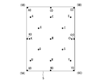
- the deposition rate and crystallinity of the microcrystalline silicon film were measured at 21 points on the substrate S as shown in FIG.
- the rough arrangement of the impedance adjusting devices 9A, 9B, 9C, and 9D connected to the upper electrode 3 arranged to face the substrate S is shown in parentheses.
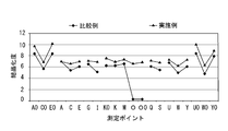
- FIG. 8 As a comparative example, the results of a similar experiment performed in a conventional plasma processing apparatus that does not have the impedance adjusting device 9 are also shown. From FIG. 8, in the plasma processing apparatus of the comparative example which does not have the impedance adjusting apparatus 9, a remarkable decrease in crystallinity was observed around the power feeding site P1. Moreover, the range which does not crystallize was observed as cloudiness. On the other hand, in the plasma processing apparatus of the embodiment in which the impedance adjustment device 9 is connected to each of the four corners of the upper electrode 3 to adjust the impedance, as in FIG. 6, the microcrystalline silicon is made around the power feeding site P1. The crystallinity was remarkably improved, and an almost uniform crystallinity was obtained in the plane of the substrate S. Moreover, white turbidity did not occur.
- the impedance adjustment device 9 is connected to a plurality of connection portions on the long side 3a of the upper electrode 3, and the capacitance is adjusted by the variable capacitor 95, whereby the efficiency of the film forming process in the plane of the substrate S is improved. It was confirmed that (the progress of crystallization) can be controlled and that a uniform crystallinity can be obtained in the plane of the substrate S. Similar results can be inferred not only for the crystallinity in the film forming process but also for the deposition rate in the film forming process and the etching rate in the etching process.
- the same result can be expected by adjusting the inductance by the variable coil 93 instead of adjusting the capacitance by the variable capacitor 95. Further, finer adjustment is possible by changing both capacitance and inductance. Furthermore, from the above experimental results, even when a fixed element is used instead of a variable element, the processing within the plane of the substrate S can be made uniform by setting so that appropriate capacitance and inductance can be obtained experimentally. It is understood that it is possible.
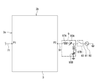
- FIG. 11 is a plan view of the upper electrode 3 showing a connection state between the upper electrode 3 and the impedance adjusting device 9 in the third embodiment.
- differences from the first embodiment will be described.
- a high-frequency power source 80 as a second high-frequency power source that supplies high-frequency power to the upper electrode 3 is connected via the impedance adjusting device 9 so that the upper electrode 3 can be fed from both sides. That is, the plasma processing apparatus of the present embodiment has a high-frequency power source 80, a power supply line 81 that feeds high-frequency power from the high-frequency power source 80, and the impedance adjustment device 9 in addition to the configuration of the first embodiment. And a relay circuit 83 interposed between the high frequency power source 80 and the high frequency power source 80.
- the impedance adjusting device 9 as shown in FIG. 11, for example, a first fixed coil 97A, a first variable capacitor 95A, a second fixed coil 97B, and a second variable capacitor 95B are provided. Use one connected in series. With such a circuit configuration, the impedance adjusting device 9 has a function as a matching circuit. As a result, impedance matching is possible when high-frequency power is supplied from the high-frequency power supply 80 to the upper electrode 3.
- the relay circuit 83 can switch between one-side power feeding to the upper electrode 3 and both-side power feeding according to the target process. That is, the relay circuit 83 is closed when the one-side power supply from the high-frequency power source 7 is performed, and the relay circuit 83 is opened when the both-side power supply from the high-frequency power source 7 and the high-frequency power source 80 is performed.
- the high frequency power supply 80 may be connected to the plurality of impedance adjusting apparatuses 9 via the relay circuits 83, respectively.
- the embodiments of the present invention have been described in detail for the purpose of illustration, but the present invention is not limited to the above-described embodiments, and various modifications are possible.
- the high frequency power is supplied to the upper electrode 3, but the high frequency power may be applied using the lower electrode 5 of the pair of parallel plate electrodes as the cathode electrode.
- the impedance adjusting device 9 may be connected to the lower electrode 5.
- the plasma processing apparatus may be configured to supply a plurality of high frequency powers having different frequencies to the pair of parallel plate electrodes.
- an impedance adjusting device can be connected to each electrode to which high frequency power is supplied, and an effective ground for each frequency component can be obtained. Therefore, it is possible to prevent high frequencies having different frequencies from flowing into the respective matching units (matching circuits) and the high frequency power source, thereby improving the high frequency power supply and the plasma stability.
Landscapes
- Chemical & Material Sciences (AREA)
- Engineering & Computer Science (AREA)
- Physics & Mathematics (AREA)
- Plasma & Fusion (AREA)
- Analytical Chemistry (AREA)
- Materials Engineering (AREA)
- Chemical Kinetics & Catalysis (AREA)
- Mechanical Engineering (AREA)
- Metallurgy (AREA)
- Organic Chemistry (AREA)
- General Chemical & Material Sciences (AREA)
- Electromagnetism (AREA)
- Spectroscopy & Molecular Physics (AREA)
- Plasma Technology (AREA)
- Chemical Vapour Deposition (AREA)
Abstract
プラズマ処理装置(100)は、矩形の基板(S)を収容する真空引き可能な処理容器(1)と、互いに対向して配置される上部電極(3)及び下部電極(5)と、上部電極(3)に高周波電力を供給する高周波電源(7)と、上部電極(3)のインピーダンスを調整するインピーダンス調整装置(9)を備えている。上部電極(3)は、長辺(3a)と短辺(3b)とを有する矩形をなしている。上部電極(3)において、高周波電源(7)から給電線(71)を介して高周波電力が供給される給電部位(P1)と、配線(91)を介してインピーダンス調整装置(9)が接続される接続部位(P2)とは、上部電極(3)における下部電極(5)との対向面(37)を間に挟んで、それぞれ反対側に形成されている。給電部位(P1)及び接続部位(P2)は、いずれも上部電極(3)の長辺(3a)の側部に設けられている。
Description
本発明は、被処理体に対してプラズマ処理を行うプラズマ処理装置及びプラズマ処理方法に関する。
液晶ディスプレイ(LCD)に代表されるフラットパネルディスプレイ(FPD)や太陽電池などの製造過程においては、大型基板に対し、エッチングや成膜等の所定の処理が施される。このような処理に用いるプラズマ処理装置として、平行平板型プラズマ処理装置が知られている。
平行平板型のプラズマ処理装置を用いて大型で大面積の基板の処理を行う場合、基板の面内での処理の均一性を確保することが重要になる。例えば、特許文献1(日本国特開平11-243062号公報)では、大面積の基板上に均一な厚みで均質な堆積膜を形成するため、長尺な板状又は棒状の電極の給電点とは反対側に、反射波電力の位相を調整する位相調整回路を接続したプラズマCVD装置が提案されている。そして、特許文献1では、一枚の基板上に、複数の長尺な高周波電極を配置することによって、基板面内での処理の均一化を図っている。
大型基板に対する処理効率を高めるため、平行平板電極を多段に積層したバッチ式の平行平板型プラズマ処理装置が検討されている。このような多段バッチ式の平行平板型プラズマ処理装置では、複数のカソードのそれぞれに対してプラズマ励起用の高周波電力を印加する必要がある。しかし、多段バッチ式の平行平板型プラズマ処理装置では、複数組の平行平板電極を処理容器内に積層して配置しなければならないため、カソードへの高周波電力の給電位置が制約される。具体的には、積層された複数のカソードへ高周波電力を供給するために、例えばカソードの片側に偏在して給電部位が設けられることになる。そのため、カソードにおける高周波電力の均一な供給が困難となり、大型基板の面内での処理の均一性を確保することが枚葉式のプラズマ処理装置に比べて難しいという問題があった。
本発明は、基板面内での処理の均一性を確保できるプラズマ処理装置を提供する。
本発明のプラズマ処理装置は、真空引き可能な処理容器と、前記処理容器内において、基板を間に挟んで互いに対向して配置されるカソード電極及びアノード電極と、を備えている。また、本発明のプラズマ処理装置は、前記カソード電極に高周波電力を供給する第1の高周波電源と、前記カソード電極に接続されて該カソード電極のインピーダンスを調整する一つ又は複数のインピーダンス調整装置と、を備えている。本発明のプラズマ処理装置は、前記カソード電極において、前記高周波電力が供給される給電部位と、前記インピーダンス調整装置が接続される接続部位のうち、少なくとも一つの接続部位とが、前記カソード電極における前記アノード電極との対向面を間に挟んで、それぞれ反対側に形成されている。
本発明のプラズマ処理装置は、一つの前記カソード電極と一つの前記アノード電極とが対をなして一つのプラズマ処理部を形成していてもよく、前記処理容器内に複数の前記プラズマ処理部が積層されて配置されていてもよい。
本発明のプラズマ処理装置において、前記カソード電極は、平面視四角形をなしていてもよく、前記給電部位が、該四角形の一辺をなす前記カソード電極の側部に設けられていてもよい。そして、本発明のプラズマ処理装置は、少なくとも一つの前記接続部位が、前記四角形の一辺とは隣接しない反対側の一辺をなす前記カソード電極の側部に設けられていてもよい。
本発明のプラズマ処理装置は、一つの前記カソード電極に対し、複数の前記インピーダンス調整装置が接続されていてもよい。この場合、本発明のプラズマ処理装置において、前記カソード電極は、平面視四角形をなしていてもよく、前記給電部位が、該四角形の一辺をなす前記カソード電極の側部に設けられていてもよい。そして、本発明のプラズマ処理装置は、前記接続部位が、前記四角形の一辺とは隣接しない反対側の一辺をなす前記カソード電極の側部の複数箇所に設けられていてもよい。この場合、少なくとも2つの前記接続部位は、前記給電部位からの距離が等しくなるように対称な位置に設けられていてもよい。
本発明のプラズマ処理装置は、前記インピーダンス調整装置を介して前記カソード電極に高周波電力を供給する第2の高周波電源をさらに備えていてもよい。
本発明のプラズマ処理装置において、前記インピーダンス調整装置は、誘導性素子と容量性素子との組み合わせを含むものであってもよい。
本発明のプラズマ処理装置は、前記誘導性素子が可変誘導性素子であってもよい。
本発明のプラズマ処理装置は、前記容量性素子が可変容量性素子であってもよい。
本発明のプラズマ処理方法は、上記いずれかのプラズマ処理装置において、前記カソード電極とアノード電極との間に基板を配置してプラズマ処理を行う。
本発明のプラズマ処理装置は、カソード電極において、高周波電力が供給される給電部位と、カソード電極のインピーダンスを調整するインピーダンス調整装置が接続される接続部位とを、カソード電極におけるアノード電極との対向面を間に挟んで、それぞれ反対側に形成した。これにより、本発明のプラズマ処理装置によれば、例えば大型で大面積の基板を処理する場合でも、基板面内での処理の均一性を確保できる。
以下、添付図面を参照しながら本発明の実施の形態に係るプラズマ処理装置について説明する。
<第1の実施の形態>
図1は、本発明の第1の実施の形態に係るプラズマ処理装置の概略構成例を示す断面図である。図1に示すように、プラズマ処理装置100は、被処理体である矩形の基板Sを収容する真空引き可能な処理容器1と、処理容器1内において、互いに対向して配置されるカソード電極としての上部電極3及びアノード電極としての下部電極5と、を備えている。また、プラズマ処理装置100は、上部電極3に高周波電力を供給する第1の高周波電源としての高周波電源7と、上部電極3に接続されて該上部電極3のインピーダンスを調整するインピーダンス調整装置9と、プラズマ処理装置100の各構成部を制御する制御部60と、を備えている。プラズマ処理装置100は、複数の基板Sに対して同時に、例えば成膜、エッチングなどを行なうバッチ式の平行平板型プラズマ処理装置として構成されている。なお、基板Sとしては、例えばFPD用のガラス基板や太陽電池用基板などを挙げることができる。FPDとしては、液晶ディスプレイ(LCD)、エレクトロルミネセンス(Electro Luminescence;EL)ディスプレイ、プラズマディスプレイパネル(PDP)等が例示される。本実施の形態のプラズマ処理装置100は、例えば短辺の長さが1mを超える大型の基板Sの処理に適している。
図1は、本発明の第1の実施の形態に係るプラズマ処理装置の概略構成例を示す断面図である。図1に示すように、プラズマ処理装置100は、被処理体である矩形の基板Sを収容する真空引き可能な処理容器1と、処理容器1内において、互いに対向して配置されるカソード電極としての上部電極3及びアノード電極としての下部電極5と、を備えている。また、プラズマ処理装置100は、上部電極3に高周波電力を供給する第1の高周波電源としての高周波電源7と、上部電極3に接続されて該上部電極3のインピーダンスを調整するインピーダンス調整装置9と、プラズマ処理装置100の各構成部を制御する制御部60と、を備えている。プラズマ処理装置100は、複数の基板Sに対して同時に、例えば成膜、エッチングなどを行なうバッチ式の平行平板型プラズマ処理装置として構成されている。なお、基板Sとしては、例えばFPD用のガラス基板や太陽電池用基板などを挙げることができる。FPDとしては、液晶ディスプレイ(LCD)、エレクトロルミネセンス(Electro Luminescence;EL)ディスプレイ、プラズマディスプレイパネル(PDP)等が例示される。本実施の形態のプラズマ処理装置100は、例えば短辺の長さが1mを超える大型の基板Sの処理に適している。
<処理容器>
処理容器1は、真空引き可能な箱型をなしている。この処理容器1は接地されている。処理容器1は、例えば、アルミニウム、アルミニウム合金、ステンレス等の金属が用いられる。処理容器1は、天井部11、角筒状の側壁部13及び底壁部15を備えている。側壁部13には、基板Sの搬入搬出時に開閉される図示しない開口が設けられており、該開口はゲートバルブによって開閉される。また、底壁部15には、排気口15aが形成されている。この排気口15aは、排気管23を介して排気装置21に接続されている。なお、排気口は、底壁部15に限らず、例えば天井部11に設けてもよい。
処理容器1は、真空引き可能な箱型をなしている。この処理容器1は接地されている。処理容器1は、例えば、アルミニウム、アルミニウム合金、ステンレス等の金属が用いられる。処理容器1は、天井部11、角筒状の側壁部13及び底壁部15を備えている。側壁部13には、基板Sの搬入搬出時に開閉される図示しない開口が設けられており、該開口はゲートバルブによって開閉される。また、底壁部15には、排気口15aが形成されている。この排気口15aは、排気管23を介して排気装置21に接続されている。なお、排気口は、底壁部15に限らず、例えば天井部11に設けてもよい。
<平行平板電極>
上部電極3及び下部電極5は、互いに平行に配置され、対をなして平行平板電極を構成している。上部電極3及び下部電極5は、いずれも、例えば、アルミニウム、アルミニウム合金、ステンレス等の金属によって形成されている。
上部電極3及び下部電極5は、互いに平行に配置され、対をなして平行平板電極を構成している。上部電極3及び下部電極5は、いずれも、例えば、アルミニウム、アルミニウム合金、ステンレス等の金属によって形成されている。
上部電極3は、処理容器1内にガスを導入するシャワーヘッドとしての機能を有している。すなわち、上部電極3は中空状をなし、その内部には、ガス拡散空間31が設けられている。また、上部電極3の下面には、処理ガスを吐出する複数のガス吐出孔33が形成されている。さらに、上部電極3の側部には、ガス拡散空間31に連通するガス導入部35が設けられている。また、上部電極3の下面は、下部電極5との対向面37を形成している。なお、上部電極3は、シャワーヘッドとしての機能を有さなくてもよく、例えば、ガス拡散空間31やガス吐出孔33を有しない平板状の金属プレートでもよい。
下部電極5は、処理容器1の側壁部13に絶縁部材や導電部材(いずれも図示省略)によって固定されている。絶縁部材で固定されている場合は、導電部材で下部電極5と側壁部13との間の導通を図ってもよい。従って、下部電極5は接地電位となっている。図1では、下部電極5と側壁部13とが導通状態にあることを導通部5aによって示している。下部電極5の上面、すなわち、上部電極3と対向する面は、基板Sを載置する基板載置面となっている。なお、下部電極5は、その基板載置面に対して突没可能な複数の基板支持ピン(図示省略)を有しており、この基板支持ピンを利用して外部の搬送装置との間で基板Sの受け渡しを行うことができる。
<プラズマ処理部>
本実施の形態のプラズマ処理装置100では、一つの上部電極3と一つの下部電極5とが対をなして一つのプラズマ処理部10を構成している。処理容器1内には、複数のプラズマ処理部10が多段に積層されて配置されている。これにより、プラズマ処理装置100では、複数枚の基板Sを同時にバッチ処理することが可能になっている。処理容器1内におけるプラズマ処理部10の数は、例えば3~20の範囲内とすることができる。
本実施の形態のプラズマ処理装置100では、一つの上部電極3と一つの下部電極5とが対をなして一つのプラズマ処理部10を構成している。処理容器1内には、複数のプラズマ処理部10が多段に積層されて配置されている。これにより、プラズマ処理装置100では、複数枚の基板Sを同時にバッチ処理することが可能になっている。処理容器1内におけるプラズマ処理部10の数は、例えば3~20の範囲内とすることができる。
<高周波電源>
上部電極3には、給電線71が接続されている。この給電線71には、整合器73を介してプラズマ形成用の高周波電源7が接続されている。これにより、高周波電源7から例えば13.56MHzの高周波電力が、上部電極3に供給される。給電線71は、処理容器1の側壁部13に形成された給電用開口13aを介して処理容器1内に導入されている。なお、給電用開口13aの周囲は図示しないベローズなどの真空保持手段が設けられている。また、高周波電力の周波数は、例えば、11MHz、27.12MHz、40.68MHz、60MHzなどでもよい。
上部電極3には、給電線71が接続されている。この給電線71には、整合器73を介してプラズマ形成用の高周波電源7が接続されている。これにより、高周波電源7から例えば13.56MHzの高周波電力が、上部電極3に供給される。給電線71は、処理容器1の側壁部13に形成された給電用開口13aを介して処理容器1内に導入されている。なお、給電用開口13aの周囲は図示しないベローズなどの真空保持手段が設けられている。また、高周波電力の周波数は、例えば、11MHz、27.12MHz、40.68MHz、60MHzなどでもよい。
整合器73内には、一端側が例えば同軸ケーブルを介して高周波電源7に接続された整合回路(図示省略)が設けられており、この整合回路の他端側は給電線71を介して上部電極3に接続されている。整合回路はプラズマのインピーダンスに合わせて負荷(プラズマ)と高周波電源7との間におけるインピーダンス調整(マッチング)を行い、プラズマ処理装置100の回路内に発生した反射波を減衰させる役割を果たす。
<インピーダンス調整装置>
本実施の形態のプラズマ処理装置100は、上部電極3毎に、上部電極3のインピーダンスを調整するインピーダンス調整装置9を備えている。各上部電極3には、配線91を介してインピーダンス調整装置9が接続されている。インピーダンス調整装置9は接地されている。ただし、インピーダンス調整装置9の接地は必須ではなく、アノード電極としての下部電極5と電気的に接続されていればよい。例えば、図1に示したように、処理容器1の側壁部13に下部電極5が導通可能に接続され、かつ、処理容器1が接地されている場合、下部電極5が接地されていることになり、インピーダンス調整装置9も接地される。
本実施の形態のプラズマ処理装置100は、上部電極3毎に、上部電極3のインピーダンスを調整するインピーダンス調整装置9を備えている。各上部電極3には、配線91を介してインピーダンス調整装置9が接続されている。インピーダンス調整装置9は接地されている。ただし、インピーダンス調整装置9の接地は必須ではなく、アノード電極としての下部電極5と電気的に接続されていればよい。例えば、図1に示したように、処理容器1の側壁部13に下部電極5が導通可能に接続され、かつ、処理容器1が接地されている場合、下部電極5が接地されていることになり、インピーダンス調整装置9も接地される。
図2は、上部電極3とインピーダンス調整装置9との接続状態を示す説明図である。図2では、上部電極3の平面図とともに、上部電極3に給電線71が接続される給電部位P1と、上部電極3に配線91を介してインピーダンス調整装置9が接続される接続部位P2とを示している。
図2に示すように、上部電極3は、四角形、例えば長辺3aと短辺3bとを有する矩形をなしている。上部電極3において、高周波電源7から給電線71を介して高周波電力が供給される給電部位P1と、配線91を介してインピーダンス調整装置9が接続される接続部位P2とは、上部電極3における下部電極5との対向面37(図1を参照)を間に挟んで、それぞれ反対側の側部に形成されている。給電部位P1及び接続部位P2は、いずれも上部電極3の長辺3aの側部に設けられている。本実施の形態では、給電部位P1及び接続部位P2は、上部電極3の長辺3aを2等分する中点付近に設けられている。
インピーダンス調整装置9は、誘導性素子と容量性素子との組み合わせを含むことができる。誘導性素子としては、例えば、ループコイル、ソレノイドコイルや直線状線材などを用いることができる。特に13.56MHz程度の高周波では、ループ状ではない直線状の線材でも誘電性素子として機能する。容量性素子としては、例えば、真空コンデンサ、セラミックコンデンサなどを用いることができる。誘導性素子は固定誘導性素子でもよいし、可変誘導性素子でもよい。また、容量性素子は、固定容量性素子でもよいし、可変容量性素子でもよい。図3A~図3Dは、インピーダンス調整装置9における誘導性素子と容量性素子との好ましい組み合わせを例示している。
図3Aは、インピーダンス調整装置9として、インダクタンスを変化させることができる可変コイル93と、キャパシタンスを変化させることができる可変コンデンサ95とを直列接続した回路である。
図3Bは、インピーダンス調整装置9として、固定コイル97と、キャパシタンスを変化させることができる可変コンデンサ95とを直列接続した回路である。
図3Cは、インピーダンス調整装置9として、インダクタンスを変化させることができる可変コイル93と、固定コンデンサ99とを直列接続した回路である。
図3Dは、インピーダンス調整装置9として、固定コイル97と、固定コンデンサ99とを直列接続した回路である。
なお、可変コイル93におけるインダクタンス及び可変コンデンサ95におけるキャパシタンスは、例えばステッピングモータ等の駆動手段を用いて調節可能であり、かつ、制御部60によって制御できるように構成されている。また、可変コイル93や可変コンデンサ95に、例えばダイヤルなどを設け、インダクタンスやキャパシタンスを手動で調整可能に構成してもよい。
図3A~図3Dに挙げた例は、いずれも、上部電極3とアースとの間で、インピーダンス調整装置9として誘導性素子と容量性素子との直列接続回路を設けている。しかし、インピーダンス調整装置9としては、上部電極3のインピーダンスを調整できる機能を有するものであれば、上記例示の回路構成に限るものではない。例えば、インピーダンス調整装置9は、インピーダンスを適切に調整できれば、誘導性素子又は容量性素子のどちらかを一つのみ含む構成でもよい。また、例えば、図3A~図3Dに挙げた組み合わせにおいて、誘導性素子と容量性素子との接続順序を入れ替えて接続することも可能である。さらに、例えば、図3A~図3Dに挙げた誘導性素子と容量性素子との直列接続の組み合わせに対し、他の誘導性素子又は容量性素子を、さらに直列に接続してもよいし、あるいは、並列に接続してもよい。
なお、本実施の形態のインピーダンス調整装置9は、上部電極3及び下部電極5による平行平板の容量成分、並びに、プラズマの容量成分に対して、それぞれ並列に接続されるため、これらの容量成分と共振しない領域で使用できる誘導性素子及び容量性素子を選択すればよい。
<排気機構>
プラズマ処理装置100は、さらに、処理容器1内を減圧排気する排気機構20を備えている。排気機構20は、例えば、ドライポンプ等の真空ポンプを有する排気装置21と、この排気装置21と排気口15aとを接続する排気管23とを備えている。排気装置21の真空ポンプを作動させることにより、処理容器1の内部空間が所定の真空度まで減圧排気される。
プラズマ処理装置100は、さらに、処理容器1内を減圧排気する排気機構20を備えている。排気機構20は、例えば、ドライポンプ等の真空ポンプを有する排気装置21と、この排気装置21と排気口15aとを接続する排気管23とを備えている。排気装置21の真空ポンプを作動させることにより、処理容器1の内部空間が所定の真空度まで減圧排気される。
<ガス供給装置>
プラズマ処理装置100は、さらに、処理容器1内にガスを供給するガス供給装置40を備えている。ガス供給装置40は、ガス供給源41と、ガス供給源41に接続され、処理容器1内に処理ガスを導入する複数の配管43(1本のみ図示)と、これら配管43に設けられた複数のバルブ45(2つのみ図示)と、マスフローコントローラ(MFC)47とを備えている。複数の配管43は、処理容器1の側壁部13のガス導入部13bを介して、上部電極3の側部に設けられたガス導入部35に接続されている。従って、ガス供給源41から、配管43、ガス導入部13b、及びガス導入部35を介して、ガス拡散空間31へ処理ガスを供給できるように構成されている。ガス拡散空間31に供給されるガスの種類や、これらのガスの流量等は、マスフローコントローラ47およびバルブ45の開閉によって制御される。なお、ガス供給装置40の代りに、プラズマ処理装置100の構成には含まれない外部のガス供給装置を使用してもよい
プラズマ処理装置100は、さらに、処理容器1内にガスを供給するガス供給装置40を備えている。ガス供給装置40は、ガス供給源41と、ガス供給源41に接続され、処理容器1内に処理ガスを導入する複数の配管43(1本のみ図示)と、これら配管43に設けられた複数のバルブ45(2つのみ図示)と、マスフローコントローラ(MFC)47とを備えている。複数の配管43は、処理容器1の側壁部13のガス導入部13bを介して、上部電極3の側部に設けられたガス導入部35に接続されている。従って、ガス供給源41から、配管43、ガス導入部13b、及びガス導入部35を介して、ガス拡散空間31へ処理ガスを供給できるように構成されている。ガス拡散空間31に供給されるガスの種類や、これらのガスの流量等は、マスフローコントローラ47およびバルブ45の開閉によって制御される。なお、ガス供給装置40の代りに、プラズマ処理装置100の構成には含まれない外部のガス供給装置を使用してもよい
<制御部>
プラズマ処理装置100の各構成部は、それぞれ制御部60に接続されて、制御部60によって制御される。制御部60は、典型的にはコンピュータである。制御部60は、CPUを備えたコントローラ61と、このコントローラ61に接続されたユーザーインターフェース62および記憶部63とを備えている。
プラズマ処理装置100の各構成部は、それぞれ制御部60に接続されて、制御部60によって制御される。制御部60は、典型的にはコンピュータである。制御部60は、CPUを備えたコントローラ61と、このコントローラ61に接続されたユーザーインターフェース62および記憶部63とを備えている。
コントローラ61は、プラズマ処理装置100において、例えば高周波出力、整合器73によるインピーダンス整合、上部電極3のインピーダンス調整、処理容器1内の圧力、ガス流量等のプロセス条件に関係する各構成部(例えば、高周波電源7、整合器73、インピーダンス調整装置9、排気装置21、ガス供給装置40等)を統括して制御する制御手段である。
ユーザーインターフェース62は、工程管理者がプラズマ処理装置100を管理するためにコマンドの入力操作等を行うキーボードやタッチパネル、プラズマ処理装置100の稼働状況を可視化して表示するディスプレイ等を有している。
記憶部63には、プラズマ処理装置100で実行される各種処理をコントローラ61の制御によって実現するための制御プログラム(ソフトウエア)や、処理条件データ等が記録されたレシピ等が保存されている。コントローラ61は、ユーザーインターフェース62からの指示等、必要に応じて、任意の制御プログラムやレシピを記憶部63から呼び出して実行する。これにより、コントローラ61による制御下で、プラズマ処理装置100の処理容器1内において所望の処理が行われる。
上記の制御プログラムおよびレシピは、例えば、CD-ROM、ハードディスク、フレキシブルディスク、フラッシュメモリ、DVD等のコンピュータ読み取り可能な記憶媒体に格納された状態のものを利用することができる。また、上記のレシピは、他の装置から、例えば専用回線を介して随時伝送させてオンラインで利用することも可能である。
次に、図4を参照しながら、本実施の形態のプラズマ処理装置100の作用について説明する。図4は、上部電極3の面内におけるVppの大きさと給電部位P1からの距離との関係を示す特性図である。ここで、Vppは、高周波電源7から上部電極3に供給される高周波電力の電圧の最大値と最小値(尖頭値;Peak to Peak)を意味する。図4の縦軸はVppの大きさを示し、横軸は高周波電源7から高周波電力が給電される給電部位P1を基準として、上部電極3の短辺方向における給電部位P1からの距離を示している。図4の横軸のP2は、図2に示したインピーダンス調整装置9の接続部位を示し、P1からP2間の距離は、上部電極3の短辺3bの長さに相当する(図2を参照)。また、図4では、上部電極3の大きさを二点鎖線で示した。なお、以下の説明では、上部電極3の二つの長辺3aのうち、給電部位P1が設けられている側を「P1側」、開放端もしくはインピーダンス調整装置9の接続部位P2が設けられている側を「P2側」と表記する。
従来技術のプラズマ処理装置では、カソードの側部から高周波電力を印加する場合、給電部位の反対側(P2側)は開放端になっていた。そのため、カソード面内のVppの分布は、図4中の曲線Aのように、カソードの短辺方向に、給電側(P1側)から開放端側(P2側)へ向けてVppが大きくなるような分布を示していた。Vppが図4中の曲線Aのような分布を持つ場合、平行平板電極間において、開放端側(P2側)に比べ、給電側(P1側)のプラズマ密度が小さくなる結果、給電側(P1側)の処理効率が低下する傾向を示した。ここで「処理効率」とは、たとえばプラズマCVDによる成膜処理なら堆積レートや結晶化度、プラズマエッチング処理ならばエッチングレートなどを意味する。
一方、本実施の形態のプラズマ処理装置100では、図2に示したように、上部電極3において、給電部位P1とは反対側の接続部位P2にインピーダンス調整装置9を接続し、接地した。ここで、インピーダンス調整装置9として、例えば図3Aに示した可変インダクタンスと可変キャパシタンスとの組み合わせの可変素子を用いことによって、給電部位P1とは反対側(P2側)のインピーダンスを細かく調整することが可能となる。
具体的には、インピーダンス調整装置9によって、給電部位P1とは反対側(P2側)のインピーダンスを誘導性インピーダンスに調整することによって、図4中の曲線Bに示したようなVppの分布を作り出すことが可能になる。曲線Bは、曲線Aに比べ、Vppのばらつきが小さく、上部電極3の短辺方向のVpp分布が均等化されている。従って、曲線BのようなVpp分布を作り出すことができれば、平行平板電極間でプラズマ密度を均一化し、基板Sの面内で均等な処理が可能になる。また、インピーダンス調整装置9によって、給電部位P1とは反対側(P2側)のインピーダンスを容量性インピーダンスに調整することによって、図4中の曲線Cに示したようなVppの分布を作り出すことも可能になる。従って、例えば、給電部位P1とは反対側(P2側)のプラズマ密度を給電側(P1側)に比べて大きくしたい場合は、インピーダンス調整装置9によって、容量性インピーダンスが強まるように調整すればよい。ここで、「誘導性インピーダンス」は、誘導性素子と容量性素子による合成のインピーダンスが誘導性に偏っていることを意味する。また、「容量性インピーダンス」は、誘導性素子と容量性素子による合成のインピーダンスが容量性に偏っていることを意味する。図4において、誘導性インピーダンスが強くなるほど、Vppの最大値は給電側(P1側)に移動していく傾向を示し、容量性インピーダンスが強くなるほど、Vppの最大値は給電部位P1とは反対側(P2側)に移動していく傾向を示す。
以上のように、インピーダンス調整装置9によって上部電極3のインピーダンスを調整して該電極におけるVpp分布を制御することができる。これによって、平行平板電極間に生成するプラズマの密度分布を調整できる。特に、プラズマ処理部10を多段に配置するために、上部電極3への給電部位P1が、下部電極5との対向面37に対して偏った位置である側部に制約されてしまう図1のプラズマ処理装置100において、インピーダンス調整装置9によってVppを平均化し、平行平板電極間でプラズマ密度を平均化できる意義は大きい。従って、インピーダンス調整装置9によって、基板Sの面内で均一な処理が可能になる。
また、インピーダンス調整装置9は、上記誘導性素子及び/又は容量性素子の定数を変えることによって、フィルタ回路としても利用できる。その場合、処理容器1内で発生する高調波成分を除去する効果が期待できることから、高調波成分による障害、例えば整合器73(整合回路)、高周波電源7等への負荷や、制御面での悪影響などを低減するという副次的な効果も期待できる。
なお、インピーダンス調整装置9として、図3Aに示した可変素子の組み合わせ以外に、図3B~図3Dに示した誘導性素子と容量性素子との組み合わせや、他の組み合わせによっても、上部電極3の短辺方向において、図4の曲線B、Cと同様のインピーダンス調整が可能である。
[処理手順]
次に、プラズマ処理装置100によって基板Sに対してプラズマCVD法による成膜処理を施す際の処理手順について説明する。まず、例えばユーザーインターフェース62から、プラズマ処理装置100において成膜処理を行うように、コントローラ61に指令が入力される。次に、コントローラ61は、この指令を受けて、記憶部63またはコンピュータ読み取り可能な記憶媒体に保存されたレシピを読み出す。次に、レシピに基づく条件によって成膜処理が実行されるように、コントローラ61からプラズマ処理装置100の各エンドデバイス(例えば、高周波電源7、整合器73、インピーダンス調整装置9、排気装置21、ガス供給装置40等)に制御信号が送出される。
次に、プラズマ処理装置100によって基板Sに対してプラズマCVD法による成膜処理を施す際の処理手順について説明する。まず、例えばユーザーインターフェース62から、プラズマ処理装置100において成膜処理を行うように、コントローラ61に指令が入力される。次に、コントローラ61は、この指令を受けて、記憶部63またはコンピュータ読み取り可能な記憶媒体に保存されたレシピを読み出す。次に、レシピに基づく条件によって成膜処理が実行されるように、コントローラ61からプラズマ処理装置100の各エンドデバイス(例えば、高周波電源7、整合器73、インピーダンス調整装置9、排気装置21、ガス供給装置40等)に制御信号が送出される。
次に、ゲートバルブ(図示省略)が開状態にされて、外部の搬送装置によって、複数の基板Sが、ゲートバルブおよび側壁部13の開口(図示省略)を通って処理容器1内に搬入される。それぞれの基板Sは、複数の基板支持ピン(図示省略)を介して下部電極5の上に載置される。次に、ゲートバルブが閉状態にされて、排気装置21によって、処理容器1内が減圧排気される。次に、ガス供給装置40によって、所定の流量の処理ガスが上部電極3のガス吐出孔33から基板Sの上面に向けて噴射される。処理容器1の内部空間は、排気量およびガス供給量を調整することによって、所定の圧力に調整される。
次に、高周波電源7から各上部電極3へ高周波電力が供給されることによって、各プラズマ処理部10において、平行平板電極をなす上部電極3と下部電極5との間に処理ガスのプラズマが生成される。生成したプラズマによって、基板Sの表面に所定の薄膜が堆積させられる。このプラズマ処理の間は、インピーダンス調整装置9によって、カソードである上部電極3におけるインピーダンスを調整することによって、基板Sにおける面内の成膜処理の均一化を図ることができる。
コントローラ61からプラズマ処理装置100の各エンドデバイスに成膜処理を終了させる制御信号が送出されると、高周波電源7からの高周波の供給が停止されると共に、処理ガスの供給が停止されて、基板Sに対する成膜処理が終了する。次に、ゲートバルブが開状態にされて、基板支持ピンによって各基板Sの高さ位置を調整した後、外部の搬送装置によって、複数の基板Sが処理容器1内から搬出される。
以上のように、プラズマ処理装置100は、例えばFPDや太陽電池の製造工程において、基板Sに対して成膜処理を行う目的で好ましく利用可能であり、また、成膜処理以外に、例えばエッチング処理などを行う場合にも利用できる。
[実験例1]
次に、本発明の効果を確認した第1の実験結果について説明する。プラズマ処理装置100と同様の構成のプラズマ処理装置を用い、基板S上にプラズマCVD法によって微結晶シリコン薄膜を形成する成膜実験を行った。この実験では、原料ガスとしてSiH4及びH2を用い、それぞれの流量[SiH4]、[H2]の比R=[H2]/[SiH4]が50以上となるような流量で処理容器1内に導入した。そして、高周波電源7から11MHzの高周波電力を上部電極3に供給することによって、上部電極3と下部電極5との間でプラズマを生成させ、基板Sの表面に約1μmの厚さの微結晶シリコン薄膜を成膜した。上部電極3は、長辺1500mm×短辺1160mmの大きさとした。上部電極3と下部電極5との間隔(ギャップ)は13mmとした。インピーダンス調整装置9は、図2に示すように、上部電極3における給電部位P1が設けられた長辺3aとは反対側の長辺3aの中点を接続部位P2として接続した。インピーダンス調整装置9としては、図3Bに示したように、固定コイル97と可変コンデンサ95とを直列接続したものを用いた。固定コイル97のインダクタンスは0.925μH、可変コンデンサ95のキャパシタンスは、63.5pFから722.1pFの範囲内で調整した。
次に、本発明の効果を確認した第1の実験結果について説明する。プラズマ処理装置100と同様の構成のプラズマ処理装置を用い、基板S上にプラズマCVD法によって微結晶シリコン薄膜を形成する成膜実験を行った。この実験では、原料ガスとしてSiH4及びH2を用い、それぞれの流量[SiH4]、[H2]の比R=[H2]/[SiH4]が50以上となるような流量で処理容器1内に導入した。そして、高周波電源7から11MHzの高周波電力を上部電極3に供給することによって、上部電極3と下部電極5との間でプラズマを生成させ、基板Sの表面に約1μmの厚さの微結晶シリコン薄膜を成膜した。上部電極3は、長辺1500mm×短辺1160mmの大きさとした。上部電極3と下部電極5との間隔(ギャップ)は13mmとした。インピーダンス調整装置9は、図2に示すように、上部電極3における給電部位P1が設けられた長辺3aとは反対側の長辺3aの中点を接続部位P2として接続した。インピーダンス調整装置9としては、図3Bに示したように、固定コイル97と可変コンデンサ95とを直列接続したものを用いた。固定コイル97のインダクタンスは0.925μH、可変コンデンサ95のキャパシタンスは、63.5pFから722.1pFの範囲内で調整した。
実験では、目視での観察およびカソードの電界分布の影響を受けやすい微結晶シリコンの結晶化度を測定した。なお、結晶化度は、ラマン分光光度計によって測定されたアモルファスシリコンピークIa(480cm-1)に対する微結晶シリコンピークIc(520cm-1)の比Ic/Iaで表した。成膜条件として、インピーダンス調整装置9を有しない従来のプラズマ処理装置では、上部電極3の給電部位P1の周囲に対向する基板S上の範囲で結晶化が困難な条件を採用し、可変コンデンサ95によってキャパシタンスを調整して成膜実験を行った。結晶化しない範囲は、反射特性の違いから、目視では白濁として観察される。その結果、キャパシタンスが63.5pF及び221.0pFでは、容量性インピーダンスを示す結果が得られた。また、キャパシタンスが385.0pF~722.1pFの範囲内では、誘導性インピーダンスを示す結果が得られた。容量性インピーダンスを示す条件では、インピーダンス調整装置9を有しない従来のプラズマ処理装置よりも、結晶化しない範囲がさらに増加した。すなわち、上部電極3の給電部位P1の周囲に対向する基板S上の結晶化しない範囲が、従来装置<63.5pF<221.0pFの順に拡大した。
一方、誘導性インピーダンスを示す条件では、インピーダンス調整装置9を有しない従来のプラズマ処理装置よりも結晶化しない範囲が減少し、特に432.5pF~563.7pFでは、基板Sの全面で良好な結晶化度が得られた。なお、385.0pFでは接続部位P2近傍に対向する基板S上に若干結晶化しない範囲が生じ、722.1pFでは給電部位P1近傍に対向する基板S上に若干結晶化しない範囲が生じた。以上の実験結果から、上部電極3の給電部位P1とは反対側の接続部位P2にインピーダンス調整装置9を接続し、可変コンデンサ95によってキャパシタンスを調整することによって、基板Sの面内での成膜処理の効率(結晶化の進行度)をコントロールできること、並びに、基板Sの面内で均一な結晶化度が得られることが確認された。同様の結果は、成膜処理における結晶化度に限らず、例えば成膜処理における堆積レートやエッチング処理におけるエッチングレートについても類推される。
なお、本実施の形態で使用するインピーダンス調整装置9では、可変コンデンサ95によるキャパシタンスの調整に代えて、可変コイル93によるインダクタンスの調整によっても同様の結果が期待できる。また、キャパシタンスとインダクタンスの両方を変化させることによって、より細かな調整が可能になる。さらに、上記実験結果から、可変素子に代えて、固定素子を用いる場合でも、実験的に適切なキャパシタンスとインダクタンスが得られるように設定することで、基板Sの面内での処理の均一化が可能であることが理解される。
以上のように、本実施の形態では、カソード電極である上部電極3において、高周波電力が供給される給電部位P1と、インピーダンス調整装置9が接続される接続部位P2とが、上部電極3における下部電極5との対向面37を間に挟んで、それぞれ反対側に形成されている。このような配置で上部電極3にインピーダンス調整装置9を設けたことによって、上部電極3におけるVppを適切に制御することができる。従って、本実施の形態のプラズマ処理装置100によれば、処理容器1内に供給される高周波電力の損失が低減され、電力の利用効率を向上させながら、基板Sの面内における処理の均一性を高めることができる。
[第2の実施の形態]
次に、図5及び図6を参照しながら、本発明の第2の実施の形態のプラズマ処理装置について説明する。図5及び図6は、第2の実施の形態における上部電極3とインピーダンス調整装置9との接続状態を示す説明図である。本実施の形態では、一つのカソード電極に対し、複数のインピーダンス調整装置9が接続されている。ここでは、第1の実施の形態との相違点について説明する。
次に、図5及び図6を参照しながら、本発明の第2の実施の形態のプラズマ処理装置について説明する。図5及び図6は、第2の実施の形態における上部電極3とインピーダンス調整装置9との接続状態を示す説明図である。本実施の形態では、一つのカソード電極に対し、複数のインピーダンス調整装置9が接続されている。ここでは、第1の実施の形態との相違点について説明する。
図5は、上部電極3に、2つのインピーダンス調整装置9を接続した態様を示す上部電極3の平面図である。図5において、2つのインピーダンス調整装置9を区別する場合に、説明の便宜上、紙面に向かって上側のインピーダンス調整装置を9A、同下側のインピーダンス調整装置を9Bと表記する。また、インピーダンス調整装置9Aの接続部位をP21、インピーダンス調整装置9Bの接続部位をP22とする。
図5に示すように、長辺3aと短辺3bとを有して矩形をなす上部電極3において、高周波電源7から給電線71を介して高周波電力が供給される給電部位P1と、配線91を介してインピーダンス調整装置9A,9Bが接続される接続部位P21,22とは、上部電極3における、下部電極5との対向面37(図1を参照)を間に挟んで、それぞれ反対側に形成されている。給電部位P1と接続部位P21,P22は、いずれも上部電極3の長辺3aの側部に設けられている。本実施の形態では、給電部位P1は、上部電極3の長辺3aを2等分する中点に設けられている。また、インピーダンス調整装置9A,9Bの接続部位P21,P22は、給電部位P1との距離が等しくなるように、それぞれ、長辺3aの端部(上部電極3の角)の近傍に設けられている。つまり、インピーダンス調整装置9A,9Bの接続部位P21,P22は、上部電極3の二つの長辺3aの中点mL,mLを通る直線M1に対して、線対称に配置されている。このように、上部電極3の長辺3a方向に、2つの接続部位P21,P22を給電部位P1に対して対称に配置することによって、上部電極3の長辺3a方向におけるVppを細かく調整できる。
本実施の形態のプラズマ処理装置では、上部電極3の一つの長辺3aに、2つのインピーダンス調整装置9A,9Bを接続することによって、上部電極3の短辺方向とともに、長辺方向においてもVppの分布を調節することができる。従って、矩形をなす基板Sの面内において、より均一なプラズマ処理が可能になる。なお、上部電極3の一つの長辺3aの3か所以上の箇所にインピーダンス調整装置9を接続することも可能である。この場合、上部電極3の長辺3aの方向においてVppをさらに細かく制御することができるため、基板Sの面内での処理の均一性を一層向上させることが可能になる。
本実施の形態では、インピーダンス調整装置9Aとインピーダンス調整装置9Bは、同じ回路構成でもよいし、異なる回路構成でもよい。また、インピーダンス調整装置9Aとインピーダンス調整装置9Bは、片方(例えばインピーダンス調整装置9A)を誘導性インピーダンスに設定し、もう一方(例えばインピーダンス調整装置9B)を容量性インピーダンスに設定する、というように、上部電極3の長辺方向において異なるインピーダンスに設定することができる。
図6は、第2の実施の形態の変形例であり、上部電極3に、4つのインピーダンス調整装置9を接続した態様を示す上部電極3の平面図である。本変形例では、長辺3aと短辺3bとを有して矩形をなす上部電極3の4隅の近傍にそれぞれインピーダンス調整装置9を配備している。すなわち、上部電極3において、高周波電源7から給電線71を介して高周波電力が供給される給電部位P1を基準に、該給電部位P1とは反対側の長辺3aに2つ、該給電部位P1と同じ側の長辺3aに2つ、合計4つのインピーダンス調整装置9を接続した。図6では、4つのインピーダンス調整装置9を区別する場合に、説明の便宜上、インピーダンス調整装置9A,9B,9C,9Dと表記する。インピーダンス調整装置9A,9Bは、上部電極3における、下部電極5との対向面37(図1を参照)を間に挟んで、給電部位P1とは反対側の長辺3aの接続部位P21,22において、それぞれ上部電極3に接続されている。また、インピーダンス調整装置9C,9Dは、上部電極3における、給電部位P1と同じ側の長辺3aの接続部位P23,24において、それぞれ上部電極3に接続されている。
図6に示す変形例では、接続部位P21とP22は、給電部位P1との距離が等しくなるように配置されている。また、接続部位P23とP24は、給電部位P1との距離が等しくなるように配置されている。つまり、インピーダンス調整装置9A,9Bの接続部位P21,P22は、上部電極3の二つの長辺3aの中点mL,mLを通る直線M1に対して、線対称に配置されている。また、インピーダンス調整装置9C,9Dの接続部位P23,P24は、直線M1に対して、線対称に配置されている。さらに、インピーダンス調整装置9A,9Cの接続部位P21,P23は、上部電極3の二つの短辺3bの中点mS,mSを通る直線M2に対して、線対称に配置されている。また、インピーダンス調整装置9B,9Dの接続部位P22,P24は、直線M2に対して、線対称に配置されている。このように、矩形の上部電極3において、4つの接続部位P21,P22,P23,P24を対称かつ均等に配置することによって、上部電極3の長辺3aの方向及び短辺3bの方向におけるVppの調整が容易になる。
本変形例では、図6に例示するように、上部電極3の二つの長辺3aに、それぞれ2つのインピーダンス調整装置9を接続することによって、上部電極3の面内におけるVppを細かく制御することができるため、基板Sの面内での処理の均一性を一層向上させることが可能になる。なお、上部電極3の一つの長辺3aにおいて、3つ以上のインピーダンス調整装置9を接続してもよい。
[実験例2]
次に、本発明の効果を確認した第2の実験結果について説明する。図6と同様に、上部電極3に4つのインピーダンス調整装置9を接続した以外は、第1の実施の形態のプラズマ処理装置100と同様の構成のプラズマ処理装置を用い、基板S上にプラズマCVD法によって微結晶シリコン薄膜を形成する成膜実験を行った。この実験では、原料ガスとしてSiH4及びH2を用い、それぞれの流量[SiH4]、[H2]の比R=[H2]/[SiH4]が50以上となるような流量で処理容器1内に導入した。そして、高周波電源7から11MHzの高周波電力を上部電極3に供給することによって、上部電極3と下部電極5との間でプラズマを生成させ、基板Sの表面に約1μmの厚さの微結晶シリコン薄膜を成膜した。上部電極3は、長辺1500mm×短辺1160mmの大きさとした。上部電極3と下部電極5との間隔(ギャップ)は13mmとした。インピーダンス調整装置9は、図6に示すように、上部電極3における給電部位P1が設けられた長辺3aの両端付近と、給電部位P1とは反対側の長辺3aの両端付近に、合計4つ接続した。インピーダンス調整装置9としては、図3Bに示したように、固定コイル97と可変コンデンサ95とを直列接続したものを用いた。固定コイル97のインダクタンスは1.1μHに設定し、可変コンデンサ95のキャパシタンスを100pFから900pFの範囲内で調整することによって上部電極3の面内のインピーダンスを調整した。
次に、本発明の効果を確認した第2の実験結果について説明する。図6と同様に、上部電極3に4つのインピーダンス調整装置9を接続した以外は、第1の実施の形態のプラズマ処理装置100と同様の構成のプラズマ処理装置を用い、基板S上にプラズマCVD法によって微結晶シリコン薄膜を形成する成膜実験を行った。この実験では、原料ガスとしてSiH4及びH2を用い、それぞれの流量[SiH4]、[H2]の比R=[H2]/[SiH4]が50以上となるような流量で処理容器1内に導入した。そして、高周波電源7から11MHzの高周波電力を上部電極3に供給することによって、上部電極3と下部電極5との間でプラズマを生成させ、基板Sの表面に約1μmの厚さの微結晶シリコン薄膜を成膜した。上部電極3は、長辺1500mm×短辺1160mmの大きさとした。上部電極3と下部電極5との間隔(ギャップ)は13mmとした。インピーダンス調整装置9は、図6に示すように、上部電極3における給電部位P1が設けられた長辺3aの両端付近と、給電部位P1とは反対側の長辺3aの両端付近に、合計4つ接続した。インピーダンス調整装置9としては、図3Bに示したように、固定コイル97と可変コンデンサ95とを直列接続したものを用いた。固定コイル97のインダクタンスは1.1μHに設定し、可変コンデンサ95のキャパシタンスを100pFから900pFの範囲内で調整することによって上部電極3の面内のインピーダンスを調整した。
実験では、目視での観察およびカソードの電界分布の影響を受けやすい微結晶シリコンの結晶化度を測定した。なお、結晶化度は、ラマン分光光度計によって測定された薄膜中のアモルファスシリコンピークIa(480cm-1)に対する微結晶シリコンピークIc(520cm-1)の比Ic/Iaで表した。成膜条件として、インピーダンス調整装置9を有しない従来のプラズマ処理装置では、上部電極3の給電部位P1の周囲に対向する基板S上の範囲で結晶化が困難な条件を採用し、可変コンデンサ95によってキャパシタンスを調整して成膜実験を行った。そして、微結晶シリコン膜の堆積レートと結晶化度を、図7に示すように基板S上の21箇所のポイントで測定した。なお、図7中には、基板Sに対向配置される上部電極3に接続されたインピーダンス調整装置9A,9B,9C,9Dの大まかな配置をカッコ書きで示した。
実験の結果を図8に示した。なお、図8には、比較例として、インピーダンス調整装置9を有しない従来のプラズマ処理装置において同様の実験を行った場合の結果を併記した。図8より、インピーダンス調整装置9を有しない比較例のプラズマ処理装置では、給電部位P1の周囲において結晶化度の著しい低下が観察された。また、結晶化しない範囲は、白濁として観察された。それに対し、図6と同様に、上部電極3の4隅にそれぞれインピーダンス調整装置9を接続し、インピーダンスの調整を行った実施例のプラズマ処理装置では、給電部位P1の周囲において、微結晶シリコンの結晶化度が顕著に改善し、基板Sの面内で、ほぼ均等な結晶化度が得られた。また、白濁は生じなかった。
[実験例3]
次に、4つのインピーダンス調整装置9A,9B,9C,9Dにおいて、可変コンデンサ95のキャパシタンスを以下の条件A~Dに設定した以外は、実験例2と同様にして成膜実験を行った。そして、微結晶シリコン膜の堆積レートと結晶化度を、図9に示すように基板S上の25箇所のポイントで測定した。なお、図9中には、基板Sに対向配置される上部電極3に接続されたインピーダンス調整装置9A,9B,9C,9Dの大まかな配置をカッコ書きで示した。
<条件A>
4つのインピーダンス調整装置9A,9B,9C,9Dの全てで可変コンデンサ95のキャパシタンスを300pFに設定した。
<条件B>
インピーダンス調整装置9B,9Dで可変コンデンサ95のキャパシタンスを400pFに設定し、インピーダンス調整装置9A,9Cで可変コンデンサ95のキャパシタンスを300pFに設定した。
<条件C>
インピーダンス調整装置9B,9Dで可変コンデンサ95のキャパシタンスを300pFに設定し、インピーダンス調整装置9A,9Cで可変コンデンサ95のキャパシタンスを400pFに設定した。
<条件D>
4つのインピーダンス調整装置9A,9B,9C,9Dの全てで可変コンデンサ95のキャパシタンスを400pFに設定した。
次に、4つのインピーダンス調整装置9A,9B,9C,9Dにおいて、可変コンデンサ95のキャパシタンスを以下の条件A~Dに設定した以外は、実験例2と同様にして成膜実験を行った。そして、微結晶シリコン膜の堆積レートと結晶化度を、図9に示すように基板S上の25箇所のポイントで測定した。なお、図9中には、基板Sに対向配置される上部電極3に接続されたインピーダンス調整装置9A,9B,9C,9Dの大まかな配置をカッコ書きで示した。
<条件A>
4つのインピーダンス調整装置9A,9B,9C,9Dの全てで可変コンデンサ95のキャパシタンスを300pFに設定した。
<条件B>
インピーダンス調整装置9B,9Dで可変コンデンサ95のキャパシタンスを400pFに設定し、インピーダンス調整装置9A,9Cで可変コンデンサ95のキャパシタンスを300pFに設定した。
<条件C>
インピーダンス調整装置9B,9Dで可変コンデンサ95のキャパシタンスを300pFに設定し、インピーダンス調整装置9A,9Cで可変コンデンサ95のキャパシタンスを400pFに設定した。
<条件D>
4つのインピーダンス調整装置9A,9B,9C,9Dの全てで可変コンデンサ95のキャパシタンスを400pFに設定した。
実験の結果を図10に示した。図10より、4つのインピーダンス調整装置9を用い、上部電極3の長辺3aの方向において別々にインピーダンスの調整を行った場合、微結晶シリコンの結晶化度が基板Sの面内で大きく変化した。また、条件Aでは、微結晶シリコン膜のほぼ全体が白濁した。条件Bでは、可変コンデンサ95のキャパシタンスを300pFに設定したインピーダンス調整装置9A,9Cの接続部位P21,P23に対向する側(図9の測定ポイント6,7,8側)で微結晶シリコン膜に白濁が観察された。条件Cでは、可変コンデンサ95のキャパシタンスを300pFに設定したインピーダンス調整装置9B,9Dの接続部位P22,P24に対向する側(図9の測定ポイント1,2,3側)で微結晶シリコン膜に白濁が観察された。条件Dでは、微結晶シリコン膜の全体において白濁は観察されなかった。つまり、4つのインピーダンス調整装置9A,9B,9C,9Dの全てで可変コンデンサ95のキャパシタンスを400pFに設定した条件Dにおいて、基板Sの面内での結晶化度の均一性が最も優れていた。
以上の実験結果から、上部電極3の長辺3aにおける複数の接続部位にインピーダンス調整装置9を接続し、可変コンデンサ95によってキャパシタンスを調整することによって、基板Sの面内での成膜処理の効率(結晶化の進行度)をコントロールできること、並びに、基板Sの面内で均一な結晶化度が得られることが確認された。同様の結果は、成膜処理における結晶化度に限らず、例えば成膜処理における堆積レートやエッチング処理におけるエッチングレートについても類推される。
なお、本実施の形態で使用するインピーダンス調整装置9では、可変コンデンサ95によるキャパシタンスの調整に代えて、可変コイル93によるインダクタンスの調整によっても同様の結果が期待できる。また、キャパシタンスとインダクタンスの両方を変化させることによって、より細かな調整が可能になる。さらに、上記実験結果から、可変素子に代えて、固定素子を用いる場合でも、実験的に適切なキャパシタンスとインダクタンスが得られるように設定することで、基板Sの面内での処理の均一化が可能であることが理解される。
本実施の形態のプラズマ処理装置における他の構成及び効果は、第1の実施の形態のプラズマ処理装置100と同様であるので説明を省略する。
[第3の実施の形態]
次に、図11を参照しながら、本発明の第3の実施の形態のプラズマ処理装置について説明する。図11は、第3の実施の形態における上部電極3とインピーダンス調整装置9との接続状態を示す上部電極3の平面図である。ここでは、第1の実施の形態との相違点について説明する。
次に、図11を参照しながら、本発明の第3の実施の形態のプラズマ処理装置について説明する。図11は、第3の実施の形態における上部電極3とインピーダンス調整装置9との接続状態を示す上部電極3の平面図である。ここでは、第1の実施の形態との相違点について説明する。
本実施の形態では、インピーダンス調整装置9を介して上部電極3に高周波電力を供給する第2の高周波電源としての高周波電源80を接続し、上部電極3へ両側からの給電を可能にしている。すなわち、本実施の形態のプラズマ処理装置は、第1の実施の形態の構成に加え、さらに、高周波電源80と、該高周波電源80からの高周波電力を給電する給電線81と、インピーダンス調整装置9と高周波電源80との間に介在配置されたリレー回路83とを備えている。
また、本実施の形態では、インピーダンス調整装置9として、例えば図11に示すように、第1の固定コイル97A、第1の可変コンデンサ95A、第2の固定コイル97B及び第2の可変コンデンサ95Bを直列に接続したものを用いる。このような回路構成によって、インピーダンス調整装置9に整合回路としての機能を持たせている。これによって、高周波電源80から上部電極3へ高周波電力を供給する場合のインピーダンス整合が可能になる。
また、本実施の形態では、リレー回路83によって、目的のプロセスに応じて、上部電極3への片側給電と、両側給電との切り替えを行うことができる。すなわち、高周波電源7からの片側給電を行う場合はリレー回路83を閉じ、高周波電源7及び高周波電源80からの両側給電を行う場合は、リレー回路83を開放すればよい。
本実施の形態のプラズマ処理装置における他の構成及び効果は、第1の実施の形態のプラズマ処理装置100と同様であるので説明を省略する。なお、第2の実施の形態のプラズマ処理装置においても、複数のインピーダンス調整装置9に対し、それぞれリレー回路83を介して高周波電源80を接続してもよい。
以上、本発明の実施の形態を例示の目的で詳細に説明したが、本発明は上記実施の形態に制約されることはなく、種々の変形が可能である。例えば、上記実施の形態のプラズマ処理装置では、上部電極3に高周波電力を供給する構成としたが、一対の平行平板電極の下部電極5をカソード電極として高周波電力を印加してもよく、その場合には、下部電極5にインピーダンス調整装置9を接続してもよい。
また、プラズマ処理装置は、一対の平行平板電極に対し、周波数が異なる複数の高周波電力を供給する構成でもよい。この場合、高周波電力が供給されるそれぞれの電極に、インピーダンス調整装置を接続することが可能であり、それぞれの周波数成分に対する効果的なグランドとすることができる。従って、異なる周波数の高周波が、それぞれの整合器(整合回路)や高周波電源に流入することを防ぎ、高周波電力供給やプラズマの安定性を向上させることができる。
本国際出願は、2013年6月24日に出願された日本国特許出願2013-131425号に基づく優先権を主張するものであり、当該出願の全内容をここに援用する。
Claims (10)
- 真空引き可能な処理容器と、
前記処理容器内において、基板を間に挟んで互いに対向して配置されるカソード電極及びアノード電極と、
前記カソード電極に高周波電力を供給する第1の高周波電源と、
前記カソード電極に接続されて該カソード電極のインピーダンスを調整する一つ又は複数のインピーダンス調整装置と、
を備え、
前記カソード電極において、前記高周波電力が供給される給電部位と、前記インピーダンス調整装置が接続される接続部位のうち、少なくとも一つの接続部位とが、前記カソード電極における前記アノード電極との対向面を間に挟んで、それぞれ反対側に形成されているプラズマ処理装置。 - 一つの前記カソード電極と一つの前記アノード電極とが対をなして一つのプラズマ処理部を形成しており、前記処理容器内に複数の前記プラズマ処理部が積層されて配置されている請求項1に記載のプラズマ処理装置。
- 前記カソード電極は、平面視四角形をなしており、
前記給電部位が、該四角形の一辺をなす前記カソード電極の側部に設けられており、
少なくとも一つの前記接続部位が、前記四角形の一辺とは隣接しない反対側の一辺をなす前記カソード電極の側部に設けられている請求項1に記載のプラズマ処理装置。 - 一つの前記カソード電極に対し、複数の前記インピーダンス調整装置が接続されている請求項1に記載のプラズマ処理装置。
- 前記カソード電極は、平面視四角形をなしており、
前記給電部位が、該四角形の一辺をなす前記カソード電極の側部に設けられており、
前記接続部位が、前記四角形の一辺とは隣接しない反対側の一辺をなす前記カソード電極の側部の複数箇所に設けられており、
少なくとも2つの前記接続部位は、前記給電部位からの距離が等しくなるように対称な位置に設けられている請求項4に記載のプラズマ処理装置。 - 前記インピーダンス調整装置を介して前記カソード電極に高周波電力を供給する第2の高周波電源をさらに備えている請求項1に記載のプラズマ処理装置。
- 前記インピーダンス調整装置は、誘導性素子と容量性素子との組み合わせを含むものである請求項1に記載のプラズマ処理装置。
- 前記誘導性素子が可変誘導性素子である請求項7に記載のプラズマ処理装置。
- 前記容量性素子が可変容量性素子である請求項7に記載のプラズマ処理装置。
- 真空引き可能な処理容器と、前記処理容器内において、基板を間に挟んで互いに対向して配置されるカソード電極及びアノード電極と、前記カソード電極に高周波電力を供給する第1の高周波電源と、前記カソード電極に接続されて該カソード電極のインピーダンスを調整する一つ又は複数のインピーダンス調整装置と、を備え、前記カソード電極において、前記高周波電力が供給される給電部位と、前記インピーダンス調整装置が接続される接続部位のうち、少なくとも一つの接続部位とが、前記カソード電極における前記アノード電極との対向面を間に挟んで、それぞれ反対側に形成されているプラズマ処理装置を用い、前記カソード電極とアノード電極との間に基板を配置してプラズマ処理を行うプラズマ処理方法。
Applications Claiming Priority (2)
| Application Number | Priority Date | Filing Date | Title |
|---|---|---|---|
| JP2013131425A JP2015005475A (ja) | 2013-06-24 | 2013-06-24 | プラズマ処理装置及びプラズマ処理方法 |
| JP2013-131425 | 2013-06-24 |
Publications (1)
| Publication Number | Publication Date |
|---|---|
| WO2014208288A1 true WO2014208288A1 (ja) | 2014-12-31 |
Family
ID=52141636
Family Applications (1)
| Application Number | Title | Priority Date | Filing Date |
|---|---|---|---|
| PCT/JP2014/064680 Ceased WO2014208288A1 (ja) | 2013-06-24 | 2014-06-03 | プラズマ処理装置及びプラズマ処理方法 |
Country Status (2)
| Country | Link |
|---|---|
| JP (1) | JP2015005475A (ja) |
| WO (1) | WO2014208288A1 (ja) |
Families Citing this family (5)
| Publication number | Priority date | Publication date | Assignee | Title |
|---|---|---|---|---|
| JP6515665B2 (ja) * | 2015-05-07 | 2019-05-22 | 東京エレクトロン株式会社 | 基板処理装置 |
| JP7516198B2 (ja) * | 2020-05-01 | 2024-07-16 | 東京エレクトロン株式会社 | エッチング装置及びエッチング方法 |
| TWI798760B (zh) | 2020-08-26 | 2023-04-11 | 日商國際電氣股份有限公司 | 基板處理裝置、半導體裝置之製造方法、基板保持具及程式 |
| WO2022250145A1 (ja) | 2021-05-27 | 2022-12-01 | 旭化成株式会社 | プラズマ発生装置、プラズマ処理装置およびシームレスローラモールド用プラズマエッチング装置 |
| JP2024021409A (ja) * | 2022-08-03 | 2024-02-16 | 東京エレクトロン株式会社 | プラズマ処理装置及びプラズマ処理方法 |
Citations (2)
| Publication number | Priority date | Publication date | Assignee | Title |
|---|---|---|---|---|
| JP2010232347A (ja) * | 2009-03-26 | 2010-10-14 | Mitsubishi Heavy Ind Ltd | 真空処理装置 |
| JP2013105543A (ja) * | 2011-11-10 | 2013-05-30 | Tokyo Electron Ltd | 基板処理装置 |
-
2013
- 2013-06-24 JP JP2013131425A patent/JP2015005475A/ja active Pending
-
2014
- 2014-06-03 WO PCT/JP2014/064680 patent/WO2014208288A1/ja not_active Ceased
Patent Citations (2)
| Publication number | Priority date | Publication date | Assignee | Title |
|---|---|---|---|---|
| JP2010232347A (ja) * | 2009-03-26 | 2010-10-14 | Mitsubishi Heavy Ind Ltd | 真空処理装置 |
| JP2013105543A (ja) * | 2011-11-10 | 2013-05-30 | Tokyo Electron Ltd | 基板処理装置 |
Also Published As
| Publication number | Publication date |
|---|---|
| JP2015005475A (ja) | 2015-01-08 |
Similar Documents
| Publication | Publication Date | Title |
|---|---|---|
| CN101730375B (zh) | 感应耦合等离子体处理装置和等离子体处理方法 | |
| US12154760B2 (en) | Inductively-coupled plasma processing apparatus | |
| JP5749020B2 (ja) | Rf電力をプラズマチャンバに結合するための装置 | |
| TWI803670B (zh) | 電漿處理裝置 | |
| JP5443127B2 (ja) | プラズマ処理装置 | |
| US20200203132A1 (en) | Plasma processing using multiple radio frequency power feeds for improved uniformity | |
| JP5666991B2 (ja) | 誘導結合プラズマ用アンテナユニットおよび誘導結合プラズマ処理装置 | |
| CN102724803A (zh) | 感应耦合等离子体处理装置 | |
| KR101351661B1 (ko) | 안테나 유닛 및 유도 결합 플라즈마 처리 장치 | |
| WO2014208288A1 (ja) | プラズマ処理装置及びプラズマ処理方法 | |
| CN103167717B (zh) | 电感耦合等离子体用天线单元和电感耦合等离子体处理装置 | |
| CN110870040B (zh) | 衬底处理方法和设备 | |
| TWI284367B (en) | Inductor-coupled plasma processing device | |
| CN102184830A (zh) | 等离子体处理装置以及等离子体处理方法 | |
| TW202312221A (zh) | 混合電漿源陣列 | |
| CN103247510B (zh) | 感应耦合等离子体处理方法和感应耦合等离子体处理装置 | |
| CN100543944C (zh) | 等离子体处理装置和等离子体处理方法 | |
| KR101666933B1 (ko) | 유도 결합 플라즈마 처리 장치의 안테나 | |
| JP2004356511A (ja) | プラズマ処理装置 | |
| JP5674871B2 (ja) | 誘導結合プラズマ処理装置 | |
| WO2014203719A1 (ja) | プラズマ処理装置及びプラズマ処理方法 | |
| US8872428B2 (en) | Plasma source with vertical gradient | |
| KR20160107147A (ko) | 유도 결합 플라즈마 처리 장치의 안테나 | |
| CN113410161A (zh) | 基片处理装置和基片处理方法 |
Legal Events
| Date | Code | Title | Description |
|---|---|---|---|
| 121 | Ep: the epo has been informed by wipo that ep was designated in this application |
Ref document number: 14818065 Country of ref document: EP Kind code of ref document: A1 |
|
| NENP | Non-entry into the national phase |
Ref country code: DE |
|
| 122 | Ep: pct application non-entry in european phase |
Ref document number: 14818065 Country of ref document: EP Kind code of ref document: A1 |