WO2014203565A1 - 液晶表示装置およびその製造方法 - Google Patents
液晶表示装置およびその製造方法 Download PDFInfo
- Publication number
- WO2014203565A1 WO2014203565A1 PCT/JP2014/054961 JP2014054961W WO2014203565A1 WO 2014203565 A1 WO2014203565 A1 WO 2014203565A1 JP 2014054961 W JP2014054961 W JP 2014054961W WO 2014203565 A1 WO2014203565 A1 WO 2014203565A1
- Authority
- WO
- WIPO (PCT)
- Prior art keywords
- liquid crystal
- pretilt
- photo
- region
- alignment film
- Prior art date
- Legal status (The legal status is an assumption and is not a legal conclusion. Google has not performed a legal analysis and makes no representation as to the accuracy of the status listed.)
- Ceased
Links
Images











Classifications
-
- G—PHYSICS
- G02—OPTICS
- G02F—OPTICAL DEVICES OR ARRANGEMENTS FOR THE CONTROL OF LIGHT BY MODIFICATION OF THE OPTICAL PROPERTIES OF THE MEDIA OF THE ELEMENTS INVOLVED THEREIN; NON-LINEAR OPTICS; FREQUENCY-CHANGING OF LIGHT; OPTICAL LOGIC ELEMENTS; OPTICAL ANALOGUE/DIGITAL CONVERTERS
- G02F1/00—Devices or arrangements for the control of the intensity, colour, phase, polarisation or direction of light arriving from an independent light source, e.g. switching, gating or modulating; Non-linear optics
- G02F1/01—Devices or arrangements for the control of the intensity, colour, phase, polarisation or direction of light arriving from an independent light source, e.g. switching, gating or modulating; Non-linear optics for the control of the intensity, phase, polarisation or colour
- G02F1/13—Devices or arrangements for the control of the intensity, colour, phase, polarisation or direction of light arriving from an independent light source, e.g. switching, gating or modulating; Non-linear optics for the control of the intensity, phase, polarisation or colour based on liquid crystals, e.g. single liquid crystal display cells
- G02F1/133—Constructional arrangements; Operation of liquid crystal cells; Circuit arrangements
- G02F1/1333—Constructional arrangements; Manufacturing methods
- G02F1/1337—Surface-induced orientation of the liquid crystal molecules, e.g. by alignment layers
- G02F1/133753—Surface-induced orientation of the liquid crystal molecules, e.g. by alignment layers with different alignment orientations or pretilt angles on a same surface, e.g. for grey scale or improved viewing angle
-
- G—PHYSICS
- G02—OPTICS
- G02F—OPTICAL DEVICES OR ARRANGEMENTS FOR THE CONTROL OF LIGHT BY MODIFICATION OF THE OPTICAL PROPERTIES OF THE MEDIA OF THE ELEMENTS INVOLVED THEREIN; NON-LINEAR OPTICS; FREQUENCY-CHANGING OF LIGHT; OPTICAL LOGIC ELEMENTS; OPTICAL ANALOGUE/DIGITAL CONVERTERS
- G02F1/00—Devices or arrangements for the control of the intensity, colour, phase, polarisation or direction of light arriving from an independent light source, e.g. switching, gating or modulating; Non-linear optics
- G02F1/01—Devices or arrangements for the control of the intensity, colour, phase, polarisation or direction of light arriving from an independent light source, e.g. switching, gating or modulating; Non-linear optics for the control of the intensity, phase, polarisation or colour
- G02F1/13—Devices or arrangements for the control of the intensity, colour, phase, polarisation or direction of light arriving from an independent light source, e.g. switching, gating or modulating; Non-linear optics for the control of the intensity, phase, polarisation or colour based on liquid crystals, e.g. single liquid crystal display cells
- G02F1/133—Constructional arrangements; Operation of liquid crystal cells; Circuit arrangements
- G02F1/1333—Constructional arrangements; Manufacturing methods
- G02F1/1335—Structural association of cells with optical devices, e.g. polarisers or reflectors
- G02F1/133528—Polarisers
-
- G—PHYSICS
- G02—OPTICS
- G02F—OPTICAL DEVICES OR ARRANGEMENTS FOR THE CONTROL OF LIGHT BY MODIFICATION OF THE OPTICAL PROPERTIES OF THE MEDIA OF THE ELEMENTS INVOLVED THEREIN; NON-LINEAR OPTICS; FREQUENCY-CHANGING OF LIGHT; OPTICAL LOGIC ELEMENTS; OPTICAL ANALOGUE/DIGITAL CONVERTERS
- G02F1/00—Devices or arrangements for the control of the intensity, colour, phase, polarisation or direction of light arriving from an independent light source, e.g. switching, gating or modulating; Non-linear optics
- G02F1/01—Devices or arrangements for the control of the intensity, colour, phase, polarisation or direction of light arriving from an independent light source, e.g. switching, gating or modulating; Non-linear optics for the control of the intensity, phase, polarisation or colour
- G02F1/13—Devices or arrangements for the control of the intensity, colour, phase, polarisation or direction of light arriving from an independent light source, e.g. switching, gating or modulating; Non-linear optics for the control of the intensity, phase, polarisation or colour based on liquid crystals, e.g. single liquid crystal display cells
- G02F1/133—Constructional arrangements; Operation of liquid crystal cells; Circuit arrangements
- G02F1/1333—Constructional arrangements; Manufacturing methods
- G02F1/1337—Surface-induced orientation of the liquid crystal molecules, e.g. by alignment layers
-
- G—PHYSICS
- G02—OPTICS
- G02F—OPTICAL DEVICES OR ARRANGEMENTS FOR THE CONTROL OF LIGHT BY MODIFICATION OF THE OPTICAL PROPERTIES OF THE MEDIA OF THE ELEMENTS INVOLVED THEREIN; NON-LINEAR OPTICS; FREQUENCY-CHANGING OF LIGHT; OPTICAL LOGIC ELEMENTS; OPTICAL ANALOGUE/DIGITAL CONVERTERS
- G02F1/00—Devices or arrangements for the control of the intensity, colour, phase, polarisation or direction of light arriving from an independent light source, e.g. switching, gating or modulating; Non-linear optics
- G02F1/01—Devices or arrangements for the control of the intensity, colour, phase, polarisation or direction of light arriving from an independent light source, e.g. switching, gating or modulating; Non-linear optics for the control of the intensity, phase, polarisation or colour
- G02F1/13—Devices or arrangements for the control of the intensity, colour, phase, polarisation or direction of light arriving from an independent light source, e.g. switching, gating or modulating; Non-linear optics for the control of the intensity, phase, polarisation or colour based on liquid crystals, e.g. single liquid crystal display cells
- G02F1/133—Constructional arrangements; Operation of liquid crystal cells; Circuit arrangements
- G02F1/1333—Constructional arrangements; Manufacturing methods
- G02F1/1337—Surface-induced orientation of the liquid crystal molecules, e.g. by alignment layers
- G02F1/13378—Surface-induced orientation of the liquid crystal molecules, e.g. by alignment layers by treatment of the surface, e.g. embossing, rubbing or light irradiation
- G02F1/133788—Surface-induced orientation of the liquid crystal molecules, e.g. by alignment layers by treatment of the surface, e.g. embossing, rubbing or light irradiation by light irradiation, e.g. linearly polarised light photo-polymerisation
-
- G—PHYSICS
- G02—OPTICS
- G02F—OPTICAL DEVICES OR ARRANGEMENTS FOR THE CONTROL OF LIGHT BY MODIFICATION OF THE OPTICAL PROPERTIES OF THE MEDIA OF THE ELEMENTS INVOLVED THEREIN; NON-LINEAR OPTICS; FREQUENCY-CHANGING OF LIGHT; OPTICAL LOGIC ELEMENTS; OPTICAL ANALOGUE/DIGITAL CONVERTERS
- G02F1/00—Devices or arrangements for the control of the intensity, colour, phase, polarisation or direction of light arriving from an independent light source, e.g. switching, gating or modulating; Non-linear optics
- G02F1/01—Devices or arrangements for the control of the intensity, colour, phase, polarisation or direction of light arriving from an independent light source, e.g. switching, gating or modulating; Non-linear optics for the control of the intensity, phase, polarisation or colour
- G02F1/13—Devices or arrangements for the control of the intensity, colour, phase, polarisation or direction of light arriving from an independent light source, e.g. switching, gating or modulating; Non-linear optics for the control of the intensity, phase, polarisation or colour based on liquid crystals, e.g. single liquid crystal display cells
- G02F1/137—Devices or arrangements for the control of the intensity, colour, phase, polarisation or direction of light arriving from an independent light source, e.g. switching, gating or modulating; Non-linear optics for the control of the intensity, phase, polarisation or colour based on liquid crystals, e.g. single liquid crystal display cells characterised by the electro-optical or magneto-optical effect, e.g. field-induced phase transition, orientation effect, guest-host interaction or dynamic scattering
-
- G—PHYSICS
- G02—OPTICS
- G02F—OPTICAL DEVICES OR ARRANGEMENTS FOR THE CONTROL OF LIGHT BY MODIFICATION OF THE OPTICAL PROPERTIES OF THE MEDIA OF THE ELEMENTS INVOLVED THEREIN; NON-LINEAR OPTICS; FREQUENCY-CHANGING OF LIGHT; OPTICAL LOGIC ELEMENTS; OPTICAL ANALOGUE/DIGITAL CONVERTERS
- G02F1/00—Devices or arrangements for the control of the intensity, colour, phase, polarisation or direction of light arriving from an independent light source, e.g. switching, gating or modulating; Non-linear optics
- G02F1/01—Devices or arrangements for the control of the intensity, colour, phase, polarisation or direction of light arriving from an independent light source, e.g. switching, gating or modulating; Non-linear optics for the control of the intensity, phase, polarisation or colour
- G02F1/13—Devices or arrangements for the control of the intensity, colour, phase, polarisation or direction of light arriving from an independent light source, e.g. switching, gating or modulating; Non-linear optics for the control of the intensity, phase, polarisation or colour based on liquid crystals, e.g. single liquid crystal display cells
- G02F1/133—Constructional arrangements; Operation of liquid crystal cells; Circuit arrangements
- G02F1/1333—Constructional arrangements; Manufacturing methods
- G02F1/133382—Heating or cooling of liquid crystal cells other than for activation, e.g. circuits or arrangements for temperature control, stabilisation or uniform distribution over the cell
-
- G—PHYSICS
- G02—OPTICS
- G02F—OPTICAL DEVICES OR ARRANGEMENTS FOR THE CONTROL OF LIGHT BY MODIFICATION OF THE OPTICAL PROPERTIES OF THE MEDIA OF THE ELEMENTS INVOLVED THEREIN; NON-LINEAR OPTICS; FREQUENCY-CHANGING OF LIGHT; OPTICAL LOGIC ELEMENTS; OPTICAL ANALOGUE/DIGITAL CONVERTERS
- G02F1/00—Devices or arrangements for the control of the intensity, colour, phase, polarisation or direction of light arriving from an independent light source, e.g. switching, gating or modulating; Non-linear optics
- G02F1/01—Devices or arrangements for the control of the intensity, colour, phase, polarisation or direction of light arriving from an independent light source, e.g. switching, gating or modulating; Non-linear optics for the control of the intensity, phase, polarisation or colour
- G02F1/13—Devices or arrangements for the control of the intensity, colour, phase, polarisation or direction of light arriving from an independent light source, e.g. switching, gating or modulating; Non-linear optics for the control of the intensity, phase, polarisation or colour based on liquid crystals, e.g. single liquid crystal display cells
- G02F1/133—Constructional arrangements; Operation of liquid crystal cells; Circuit arrangements
- G02F1/1333—Constructional arrangements; Manufacturing methods
- G02F1/1335—Structural association of cells with optical devices, e.g. polarisers or reflectors
- G02F1/133528—Polarisers
- G02F1/133531—Polarisers characterised by the arrangement of polariser or analyser axes
-
- G—PHYSICS
- G02—OPTICS
- G02F—OPTICAL DEVICES OR ARRANGEMENTS FOR THE CONTROL OF LIGHT BY MODIFICATION OF THE OPTICAL PROPERTIES OF THE MEDIA OF THE ELEMENTS INVOLVED THEREIN; NON-LINEAR OPTICS; FREQUENCY-CHANGING OF LIGHT; OPTICAL LOGIC ELEMENTS; OPTICAL ANALOGUE/DIGITAL CONVERTERS
- G02F1/00—Devices or arrangements for the control of the intensity, colour, phase, polarisation or direction of light arriving from an independent light source, e.g. switching, gating or modulating; Non-linear optics
- G02F1/01—Devices or arrangements for the control of the intensity, colour, phase, polarisation or direction of light arriving from an independent light source, e.g. switching, gating or modulating; Non-linear optics for the control of the intensity, phase, polarisation or colour
- G02F1/13—Devices or arrangements for the control of the intensity, colour, phase, polarisation or direction of light arriving from an independent light source, e.g. switching, gating or modulating; Non-linear optics for the control of the intensity, phase, polarisation or colour based on liquid crystals, e.g. single liquid crystal display cells
- G02F1/133—Constructional arrangements; Operation of liquid crystal cells; Circuit arrangements
- G02F1/1333—Constructional arrangements; Manufacturing methods
- G02F1/1335—Structural association of cells with optical devices, e.g. polarisers or reflectors
- G02F1/133528—Polarisers
- G02F1/133541—Circular polarisers
-
- G—PHYSICS
- G02—OPTICS
- G02F—OPTICAL DEVICES OR ARRANGEMENTS FOR THE CONTROL OF LIGHT BY MODIFICATION OF THE OPTICAL PROPERTIES OF THE MEDIA OF THE ELEMENTS INVOLVED THEREIN; NON-LINEAR OPTICS; FREQUENCY-CHANGING OF LIGHT; OPTICAL LOGIC ELEMENTS; OPTICAL ANALOGUE/DIGITAL CONVERTERS
- G02F1/00—Devices or arrangements for the control of the intensity, colour, phase, polarisation or direction of light arriving from an independent light source, e.g. switching, gating or modulating; Non-linear optics
- G02F1/01—Devices or arrangements for the control of the intensity, colour, phase, polarisation or direction of light arriving from an independent light source, e.g. switching, gating or modulating; Non-linear optics for the control of the intensity, phase, polarisation or colour
- G02F1/13—Devices or arrangements for the control of the intensity, colour, phase, polarisation or direction of light arriving from an independent light source, e.g. switching, gating or modulating; Non-linear optics for the control of the intensity, phase, polarisation or colour based on liquid crystals, e.g. single liquid crystal display cells
- G02F1/133—Constructional arrangements; Operation of liquid crystal cells; Circuit arrangements
- G02F1/1333—Constructional arrangements; Manufacturing methods
- G02F1/1337—Surface-induced orientation of the liquid crystal molecules, e.g. by alignment layers
- G02F1/133742—Surface-induced orientation of the liquid crystal molecules, e.g. by alignment layers for homeotropic alignment
-
- G—PHYSICS
- G02—OPTICS
- G02F—OPTICAL DEVICES OR ARRANGEMENTS FOR THE CONTROL OF LIGHT BY MODIFICATION OF THE OPTICAL PROPERTIES OF THE MEDIA OF THE ELEMENTS INVOLVED THEREIN; NON-LINEAR OPTICS; FREQUENCY-CHANGING OF LIGHT; OPTICAL LOGIC ELEMENTS; OPTICAL ANALOGUE/DIGITAL CONVERTERS
- G02F1/00—Devices or arrangements for the control of the intensity, colour, phase, polarisation or direction of light arriving from an independent light source, e.g. switching, gating or modulating; Non-linear optics
- G02F1/01—Devices or arrangements for the control of the intensity, colour, phase, polarisation or direction of light arriving from an independent light source, e.g. switching, gating or modulating; Non-linear optics for the control of the intensity, phase, polarisation or colour
- G02F1/13—Devices or arrangements for the control of the intensity, colour, phase, polarisation or direction of light arriving from an independent light source, e.g. switching, gating or modulating; Non-linear optics for the control of the intensity, phase, polarisation or colour based on liquid crystals, e.g. single liquid crystal display cells
- G02F1/133—Constructional arrangements; Operation of liquid crystal cells; Circuit arrangements
- G02F1/1333—Constructional arrangements; Manufacturing methods
- G02F1/1337—Surface-induced orientation of the liquid crystal molecules, e.g. by alignment layers
- G02F1/133753—Surface-induced orientation of the liquid crystal molecules, e.g. by alignment layers with different alignment orientations or pretilt angles on a same surface, e.g. for grey scale or improved viewing angle
- G02F1/133757—Surface-induced orientation of the liquid crystal molecules, e.g. by alignment layers with different alignment orientations or pretilt angles on a same surface, e.g. for grey scale or improved viewing angle with different alignment orientations
-
- G—PHYSICS
- G02—OPTICS
- G02F—OPTICAL DEVICES OR ARRANGEMENTS FOR THE CONTROL OF LIGHT BY MODIFICATION OF THE OPTICAL PROPERTIES OF THE MEDIA OF THE ELEMENTS INVOLVED THEREIN; NON-LINEAR OPTICS; FREQUENCY-CHANGING OF LIGHT; OPTICAL LOGIC ELEMENTS; OPTICAL ANALOGUE/DIGITAL CONVERTERS
- G02F1/00—Devices or arrangements for the control of the intensity, colour, phase, polarisation or direction of light arriving from an independent light source, e.g. switching, gating or modulating; Non-linear optics
- G02F1/01—Devices or arrangements for the control of the intensity, colour, phase, polarisation or direction of light arriving from an independent light source, e.g. switching, gating or modulating; Non-linear optics for the control of the intensity, phase, polarisation or colour
- G02F1/13—Devices or arrangements for the control of the intensity, colour, phase, polarisation or direction of light arriving from an independent light source, e.g. switching, gating or modulating; Non-linear optics for the control of the intensity, phase, polarisation or colour based on liquid crystals, e.g. single liquid crystal display cells
- G02F1/133—Constructional arrangements; Operation of liquid crystal cells; Circuit arrangements
- G02F1/1333—Constructional arrangements; Manufacturing methods
- G02F1/1337—Surface-induced orientation of the liquid crystal molecules, e.g. by alignment layers
- G02F1/133753—Surface-induced orientation of the liquid crystal molecules, e.g. by alignment layers with different alignment orientations or pretilt angles on a same surface, e.g. for grey scale or improved viewing angle
- G02F1/133761—Surface-induced orientation of the liquid crystal molecules, e.g. by alignment layers with different alignment orientations or pretilt angles on a same surface, e.g. for grey scale or improved viewing angle with different pretilt angles
-
- G—PHYSICS
- G02—OPTICS
- G02F—OPTICAL DEVICES OR ARRANGEMENTS FOR THE CONTROL OF LIGHT BY MODIFICATION OF THE OPTICAL PROPERTIES OF THE MEDIA OF THE ELEMENTS INVOLVED THEREIN; NON-LINEAR OPTICS; FREQUENCY-CHANGING OF LIGHT; OPTICAL LOGIC ELEMENTS; OPTICAL ANALOGUE/DIGITAL CONVERTERS
- G02F1/00—Devices or arrangements for the control of the intensity, colour, phase, polarisation or direction of light arriving from an independent light source, e.g. switching, gating or modulating; Non-linear optics
- G02F1/01—Devices or arrangements for the control of the intensity, colour, phase, polarisation or direction of light arriving from an independent light source, e.g. switching, gating or modulating; Non-linear optics for the control of the intensity, phase, polarisation or colour
- G02F1/13—Devices or arrangements for the control of the intensity, colour, phase, polarisation or direction of light arriving from an independent light source, e.g. switching, gating or modulating; Non-linear optics for the control of the intensity, phase, polarisation or colour based on liquid crystals, e.g. single liquid crystal display cells
- G02F1/137—Devices or arrangements for the control of the intensity, colour, phase, polarisation or direction of light arriving from an independent light source, e.g. switching, gating or modulating; Non-linear optics for the control of the intensity, phase, polarisation or colour based on liquid crystals, e.g. single liquid crystal display cells characterised by the electro-optical or magneto-optical effect, e.g. field-induced phase transition, orientation effect, guest-host interaction or dynamic scattering
- G02F1/13712—Devices or arrangements for the control of the intensity, colour, phase, polarisation or direction of light arriving from an independent light source, e.g. switching, gating or modulating; Non-linear optics for the control of the intensity, phase, polarisation or colour based on liquid crystals, e.g. single liquid crystal display cells characterised by the electro-optical or magneto-optical effect, e.g. field-induced phase transition, orientation effect, guest-host interaction or dynamic scattering the liquid crystal having negative dielectric anisotropy
Definitions
- the present invention relates to a liquid crystal display device, and more particularly, to a liquid crystal display device that includes a vertical alignment type liquid crystal layer and in which a pretilt direction of liquid crystal molecules is defined by a photo alignment film.
- the present invention also relates to a method for manufacturing a liquid crystal display device.
- liquid crystal display devices have been improved, and their use in television receivers and the like has progressed. Although the viewing angle characteristics of liquid crystal display devices have been improved, further improvements are desired. In particular, there is a strong demand for improving the viewing angle characteristics of a liquid crystal display device using a vertical alignment type liquid crystal layer (sometimes referred to as a VA mode liquid crystal display device).
- a vertical alignment type liquid crystal layer sometimes referred to as a VA mode liquid crystal display device.
- VA mode liquid crystal display devices currently used in large display devices such as televisions employ an alignment division structure in which a plurality of liquid crystal domains are formed in one pixel in order to improve viewing angle characteristics. .
- the MVA mode is the mainstream.
- the MVA mode is disclosed in Patent Document 1, for example.
- a plurality of liquid crystal domains having different alignment directions (tilt directions) in each pixel are provided by providing an alignment regulating structure on each liquid crystal layer side of a pair of substrates facing each other with a vertical alignment type liquid crystal layer interposed therebetween. Specifically, four types of orientation directions are formed.
- the alignment regulating structure slits (openings) provided in the electrodes and ribs (projection structure) are used, and the alignment regulating force is exhibited from both sides of the liquid crystal layer.
- the slits and ribs are linear, so that the alignment regulating force on the liquid crystal molecules is not sufficient in the pixel. Since it becomes uniform, there exists a problem that distribution arises in a response speed. In addition, since the light transmittance of the region where the slits and ribs are provided is lowered, there is also a problem that display luminance is lowered.
- an alignment division structure in the VA mode liquid crystal display device by defining the pretilt direction with the alignment film.
- the applicant of the present application has proposed a VA mode liquid crystal display device in which an alignment division structure is formed as described above in Patent Document 2.
- a quadrant alignment structure is formed by defining a pretilt direction with an alignment film. That is, when a voltage is applied to the liquid crystal layer, four liquid crystal domains are formed in one pixel.
- Such a quadrant alignment structure is sometimes simply referred to as a 4D structure.
- a pretilt direction defined by one alignment film of a pair of alignment films opposed via a liquid crystal layer and a pretilt defined by the other alignment film are provided.
- the directions differ from each other by approximately 90 °. Therefore, when a voltage is applied, the liquid crystal molecules are twisted.
- the VA mode in which the liquid crystal molecules are twisted by using a pair of vertical alignment films provided so that the pretilt directions (alignment processing directions) are orthogonal to each other is a VATN (Vertical Alignment Twisted Nematic) mode or an RTN mode. Also called (Reverse Twisted Nematic) mode.
- the applicant of the present application calls the display mode of the liquid crystal display device of Patent Document 2 as the 4D-RTN mode.
- Patent Document 2 As a specific method for defining the pretilt direction of the liquid crystal molecules in the alignment film, as described in Patent Document 2, a method of performing photo-alignment treatment is promising. Since the photo-alignment treatment can be performed in a non-contact manner, there is no generation of static electricity due to friction unlike the rubbing treatment, and the yield can be improved.
- a VATN mode liquid crystal display device using an alignment film (photo-alignment film) subjected to photo-alignment treatment is also disclosed in Patent Document 3.
- the present invention has been made in view of the above problems, and an object of the present invention is a VA mode liquid crystal display device in which the pretilt direction of liquid crystal molecules is defined by a photo-alignment film, which is suitable for high definition. To provide an apparatus.
- a liquid crystal display device includes a first substrate and a second substrate disposed so as to face each other, and a vertical alignment type liquid crystal layer provided between the first substrate and the second substrate.
- a liquid crystal display device having a plurality of pixels arranged in a matrix, wherein the first substrate includes a pixel electrode provided in each of the plurality of pixels, and a space between the pixel electrode and the liquid crystal layer.
- a second photo-alignment film provided between the counter electrode and the liquid crystal layer; and a second photo-alignment film provided between the counter electrode and the liquid crystal layer.
- the first photo-alignment film includes a first pretilt region that defines a first pretilt direction and a second pretilt direction that is antiparallel to the first pretilt direction in each of the plurality of pixels.
- the second photo-alignment film defines a third pretilt region defining a third pretilt direction and a fourth pretilt direction antiparallel to the third pretilt direction in each of the plurality of pixels.
- a fourth pretilt region and when viewed from the normal direction of the display surface, the entire boundary between the first pretilt region and the second pretilt region of the first photoalignment film, and the second photoalignment film of the second photoalignment film The entire boundary between the third pre-tilt region and the fourth pre-tilt region overlaps.
- the first pre-tilt region of the first photo-alignment film and the third pre-tilt region of the second photo-alignment film overlap each other when viewed from the normal direction of the display surface, and the first light
- the second pretilt region of the alignment film and the fourth pretilt region of the second photo-alignment film are overlapped, and the third pretilt direction is antiparallel to the first pretilt direction, and the fourth pretilt direction Is antiparallel to the second pretilt direction.
- an outer edge of the pixel electrode includes a first edge portion and a second edge portion, and a direction orthogonal to the first edge portion and toward the inside of the pixel electrode is opposite to the first pretilt direction.
- the direction perpendicular to the second edge portion and toward the inside of the pixel electrode is a direction opposite to the second pretilt direction.
- liquid crystal domains are formed in the liquid crystal layer in each of the plurality of pixels, and each of the four liquid crystal domains is formed.
- the directions of the four directors representing the alignment direction of the liquid crystal molecules contained in are different from each other.
- the four liquid crystal domains include a first liquid crystal domain in which the director direction is the first orientation, a second liquid crystal domain in which the second orientation is, a third liquid crystal domain in which the third orientation is provided, A fourth liquid crystal domain having four orientations, wherein a difference between any two of the first orientation, the second orientation, the third orientation, and the fourth orientation is approximately an integral multiple of 90 °; equal.
- the first azimuth is approximately 0 °, approximately 90 °, approximately 180 °, or approximately 270 °.
- the above-described liquid crystal display device further includes a pair of linearly polarizing plates that are opposed to each other with the liquid crystal layer interposed therebetween and that have respective transmission axes substantially orthogonal to each other, and the pair of linearly polarized light
- the transmission axis of the plate forms an angle of approximately 45 ° with the first pretilt direction.
- the above-described liquid crystal display device further includes a pair of circularly polarizing plates facing each other with the liquid crystal layer interposed therebetween.
- the liquid crystal layer includes liquid crystal molecules having negative dielectric anisotropy.
- the shorter one of the pixel pitch along the horizontal direction of the display surface and the pixel pitch along the vertical direction of the display surface is 42 ⁇ m or less.
- the screen resolution is 200 ppi or higher.
- a method of manufacturing a liquid crystal display device includes a first substrate and a second substrate disposed so as to face each other, and a vertical alignment type provided between the first substrate and the second substrate.
- the second substrate has a counter electrode facing the pixel electrode, and a second photo-alignment film provided between the counter electrode and the liquid crystal layer.
- a method for manufacturing a display device comprising: a first pretilt region defining a first pretilt direction in a region corresponding to each of the plurality of pixels of the first photoalignment film; Parallel second pretilt direction A step (A) of forming a second pre-tilt region to be defined by photo-alignment treatment; and a third pre-tilt direction in a region corresponding to each of the plurality of pixels of the second photo-alignment film.
- the step (A) and the step (B) include the first substrate and the step in the step (C).
- the above-described method for manufacturing a liquid crystal display device further includes a step (D) of performing a realignment treatment including a heat treatment on the liquid crystal layer after the step (C), and the heat treatment includes: It is performed at 110 ° C. or lower.
- a VA mode liquid crystal display device in which the pretilt direction of liquid crystal molecules is defined by a photo-alignment film, which is suitable for high definition.
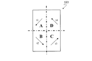
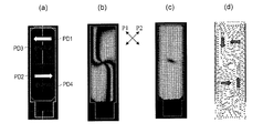
- FIG. 11 is a diagram showing an alignment division structure of a pixel 1001 in a 4D-RTN mode liquid crystal display device.
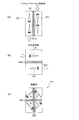
- (A), (b), and (c) are the figures for demonstrating the method for obtaining the orientation division structure of the pixel 1001 shown in FIG.
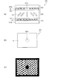
- FIG. 3 is a diagram showing an alignment division structure of a pixel 1 in the liquid crystal display device 100.
- (A), (b), and (c) are the figures for demonstrating the method for obtaining the orientation division structure of the pixel 1 shown in FIG.
- FIG. 4 is a diagram for explaining the reason why four liquid crystal domains are formed in the pixel 1 of the liquid crystal display device 100.
- FIG. (A) And (b) is a figure for demonstrating the reason why four liquid crystal domains are formed in the pixel 1 of the liquid crystal display device 100.
- FIG. (A), (b), and (c) are the figures for demonstrating the reason why four liquid crystal domains are formed in the pixel 1 of the liquid crystal display device 100.
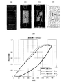
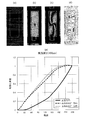
- FIG. (A)-(e) is a figure for demonstrating the result of the orientation simulation about Example 1, and an optical simulation.
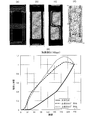
- (A)-(e) is a figure for demonstrating the result of the orientation simulation about Example 2, and an optical simulation.
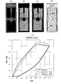
- (A)-(e) is a figure for demonstrating the result of the orientation simulation about Example 3, and an optical simulation.
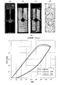
- (A)-(e) is a figure for demonstrating the result of the orientation simulation about Example 4, and an optical simulation.
- (A)-(e) is a figure for demonstrating the result of the orientation simulation about Example 5, and an optical simulation.
- (A)-(e) is a figure for demonstrating the result of the orientation simulation about Example 6, and an optical simulation.
- (A)-(e) is a figure for demonstrating the result of the orientation simulation about the comparative example 1, and an optical simulation.
- (A), (b) and (c) is a figure which shows the orientation distribution in the pixel in the comparative example 1, Example 6, and Example 2, respectively.
- (A) and (b) show the relationship between the gradation and the luminance (standardized luminance) in Example 7 and Comparative Example 2, respectively, when observed from the front direction, when viewed from the 60 ° oblique direction, and up and down.
- (A) And (b) is sectional drawing and the top view which show typically one pixel of the liquid crystal display device 900 of CPA mode, (c) is a white voltage to the liquid crystal layer 930 of the liquid crystal display device 900. It is a figure which shows the simulation result of the transmittance
- (A), (b) and (c) is a figure for demonstrating the result of having verified formation of the defective tilt area
- FIG. 10 is an optical microscope image corresponding to one pixel 1 in Example 7.
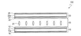
- FIG. 1 shows a liquid crystal display device 100 according to this embodiment.
- FIG. 1 is a cross-sectional view schematically showing the liquid crystal display device 100.
- the liquid crystal display device 100 includes an active matrix substrate (first substrate) 10 and a counter substrate (second substrate) 20 that are arranged to face each other, and an active matrix substrate 10 and a counter substrate 20. And a liquid crystal layer 30 provided therebetween.
- the liquid crystal display device 100 further includes a plurality of pixels arranged in a matrix.
- the plurality of pixels include a red pixel that displays red, a green pixel that displays green, and a blue pixel that displays blue, and one color display by three pixels of the red pixel, the green pixel, and the blue pixel.
- a pixel is constructed.
- An active matrix substrate (also referred to as “TFT substrate”) 10 includes a pixel electrode 11 provided in each of a plurality of pixels, and a first photo-alignment film 12 provided between the pixel electrode 11 and the liquid crystal layer 30. .
- the pixel electrode 11 and the first photo-alignment film 12 are supported by an insulating transparent substrate (for example, a glass substrate) 10a.
- the active matrix substrate includes a thin film transistor (TFT) electrically connected to the pixel electrode 11, a scanning wiring (gate bus line) for supplying a scanning signal to the TFT, and a display signal to the TFT.
- the counter substrate 20 also referred to as “color filter substrate”) 20 includes a counter electrode 21 facing the pixel electrode 11 and a second photo-alignment film 22 provided between the counter electrode 21 and the liquid crystal layer 30.
- the counter electrode 21 and the second photo-alignment film 22 are supported by an insulating transparent substrate (for example, a glass substrate) 20a.
- the counter substrate 20 has a color filter layer.
- the color filter layer includes a red color filter provided corresponding to the red pixel, a green color filter provided corresponding to the green pixel, and a blue color filter provided corresponding to the blue pixel. .
- the liquid crystal layer 30 is a vertical alignment type liquid crystal layer including liquid crystal molecules 31 having negative dielectric anisotropy. In a state where no voltage is applied to the liquid crystal layer 30, the liquid crystal molecules 31 are aligned substantially perpendicular to the substrate surface, as shown in FIG.
- the liquid crystal display device 100 further includes a pair of linearly polarizing plates 18 and 28 facing each other with at least the liquid crystal layer 30 interposed therebetween.
- the linearly polarizing plates 18 and 28 are arranged so that their transmission axes are substantially orthogonal to each other. That is, the linearly polarizing plates 18 and 28 are arranged in crossed Nicols.
- a pair of circularly polarizing plates may be provided. That is, the light incident on the liquid crystal layer 30 may be linearly polarized light or circularly polarized light.
- Each of the first photo-alignment film 12 and the second photo-alignment film 22 is a vertical alignment film that has been subjected to a photo-alignment process, and defines the pretilt direction of the liquid crystal molecules 31.
- the first photo-alignment film 12 has two regions that define different pretilt directions in each pixel.
- the second photo-alignment film 22 has two regions that define different pretilt directions in each pixel.
- FIG. 2 shows an alignment division structure of the pixel 1001 in a general 4D-RTN mode liquid crystal display device.
- four liquid crystal domains A, B, C, and D are formed in the pixel 1001 as shown in FIG.
- the four liquid crystal domains A, B, C and D are arranged in a matrix of 2 rows and 2 columns.
- the orientations of the directors t1, t2, t3, and t4 of the liquid crystal domains A, B, C, and D are four orientations in which the difference between any two directions is substantially equal to an integral multiple of 90 °.
- Directors t1, t2, t3 and t4 represent the orientation directions of the liquid crystal molecules contained in each liquid crystal domain. In the 4D-RTN mode, the directors t1, t2, t3 and t4 This is the tilt direction of the liquid crystal molecules near the center in the thickness direction.
- Each liquid crystal domain is characterized by the director orientation (tilt direction described above), and the director orientation has a dominant influence on the viewing angle dependency of each domain.
- the pair of polarizing plates facing each other through the liquid crystal layer are arranged so that the transmission axes (polarization axes) are orthogonal to each other. More specifically, one transmission axis is on the display surface. It is arranged so that it is parallel to the horizontal direction and the other transmission axis is parallel to the vertical direction of the display surface.
- the orientation of the director t1 of the liquid crystal domain A is about 225 °
- the orientation of the director t2 of the liquid crystal domain B is about 315 °
- the liquid crystal domain C The direction of the director t3 is about 45 °
- the direction of the director t4 of the liquid crystal domain D is about 135 °.
- the liquid crystal domains A, B, C, and D are arranged so that the direction of each director differs by approximately 90 ° between adjacent liquid crystal domains.
- FIG. 3A shows the pretilt directions PD1 and PD2 defined by the photo-alignment film provided on the active matrix substrate
- FIG. 3B is defined by the photo-alignment film provided on the counter substrate.
- the pretilt directions PD3 and PD4 are shown.
- FIG. 3C shows a tilt direction (director) when a voltage is applied to the liquid crystal layer.
- the region on the active matrix substrate side (region corresponding to one pixel 1001) is divided into left and right parts, and the photo-alignment film in each region (left region and right region) Photo-alignment processing is performed so that the (vertical alignment film) defines the pretilt directions PD1 and PD2 that are antiparallel to each other.
- the photo-alignment process is performed by obliquely irradiating ultraviolet rays from the direction indicated by the arrow.
- the area on the counter substrate side (area corresponding to one pixel area 1001) is vertically divided into two areas, and each area (upper area and lower area) is divided.
- the photo-alignment process is performed so that the photo-alignment film (vertical alignment film) defines the pretilt directions PD3 and PD4 that are antiparallel to each other.
- the photo-alignment process is performed by obliquely irradiating ultraviolet rays from the direction indicated by the arrow.
- the active matrix substrate and the counter substrate that have been subjected to the photo-alignment treatment are bonded to each other, thereby forming an alignment-divided pixel 1001 as shown in FIG. be able to.
- the pretilt direction defined by the photo-alignment film of the active matrix substrate and the photo-alignment film of the counter substrate are defined.
- the pretilt direction differs from the pretilt direction by approximately 90 °, and the tilt direction (the direction of the director of each liquid crystal domain) is defined in the middle of the two pretilt directions.
- the ultraviolet irradiation is performed from different directions.
- an area where a sufficient pretilt angle cannot be provided around the exposure seam (the boundary between two areas having different pretilt directions) due to light diffraction. (Hereinafter referred to as “defective tilt region”).
- the “pretilt angle” refers to an angle formed by the major axis of the liquid crystal molecules 31 with respect to the normal direction of the substrate surface when no voltage is applied.
- each pixel 1001 includes a portion extending in the vertical direction (corresponding to the defective tilt region NGR1) and a portion extending in the horizontal direction (corresponding to the defective tilt region NGR2).
- a cross-shaped defective tilt region NGR is formed.
- FIG. 4 shows an alignment division structure of the pixel 1 in the liquid crystal display device 100.
- the orientation of the director t1 of the liquid crystal domain A is about 270 °
- the orientation of the director t2 of the liquid crystal domain B is about 0 °
- the liquid crystal domain C The direction of the director t3 is approximately 90 °
- the direction of the director t4 of the liquid crystal domain D is approximately 180 °. That is, the difference between any two of the four director directions of the liquid crystal domains A, B, C, and D is substantially equal to an integral multiple of 90 °.
- the transmission axes (polarization axes) P1 and P2 of the pair of linearly polarizing plates 18 and 28 form an angle of approximately 45 ° with the orientations of the directors t1, t2, t3, and t4 of the liquid crystal domains A, B, C, and D.
- the transmission axes P1 and P2 of the pair of linearly polarizing plates 18 and 28 are approximately 45 ° in both the pretilt direction defined by the first photoalignment film 12 and the second photoalignment film 22. The corner of the.
- FIG. 4 illustrates a case where the areas occupied by the four liquid crystal domains A, B, C, and D in the pixel 1 are equal to each other, but the areas of the four liquid crystal domains A, B, C, and D are as follows. It does not have to be equal to each other. However, from the viewpoint of uniformity of viewing angle characteristics, it is preferable that the difference in area between the four liquid crystal domains A, B, C, and D is as small as possible. Specifically, the four liquid crystal domains A, B, C, and The difference between the area of the largest liquid crystal domain in D and the area of the smallest liquid crystal domain is preferably 50% or less of the largest area.
- the example shown in FIG. 4 is an example of the most preferable (ie, ideal) quadrant structure in view angle characteristics.
- FIG. 5A shows the pretilt directions PD1 and PD2 defined by the first photo-alignment film 12 provided on the active matrix substrate 10
- FIG. 5B shows the first tilt direction provided on the counter substrate 20.
- the pretilt directions PD3 and PD4 defined by the two-light alignment film 22 are shown.
- FIG. 5C shows the tilt direction (director) when a voltage is applied to the liquid crystal layer 30.
- the first photo-alignment film 12 includes a first pretilt region 12a that defines the first pretilt direction PD1 and a second antiparallel to the first pretilt direction PD1. And a second pretilt region 12b that defines a pretilt direction PD2.
- the region corresponding to one pixel 1 of the first photo-alignment film 12 is divided into two vertically, and the respective regions (first pretilt region and second pretilt region) 12a and 12b are opposite to each other.
- Photo-alignment processing is performed so as to define parallel pretilt directions (first pretilt direction and second pretilt direction) PD1 and PD2.
- the photo-alignment treatment is performed by obliquely irradiating ultraviolet rays from the direction indicated by the arrow.
- the second photo-alignment film 22 is antiparallel to the third pretilt direction PD3 and the third pretilt region 22a that defines the third pretilt direction PD3, as shown in FIG. And a fourth pretilt region 22b that defines a fourth pretilt direction PD4.
- the region corresponding to one pixel 1 of the second photo-alignment film 22 is divided into two vertically, and the respective regions (third pre-tilt region and fourth pre-tilt region) 22a and 22b are opposite to each other.
- Photo-alignment processing is performed so as to define the parallel pretilt directions (third pretilt direction and fourth pretilt direction) PD3 and PD4.
- the photo-alignment treatment is performed by obliquely irradiating ultraviolet rays from the direction indicated by the arrow.
- the third pre-tilt region 22a of the second photo-alignment film 22 is the first pre-alignment film 12 of the first photo-alignment film 12 when viewed from the normal direction of the display surface.
- the fourth pretilt region 22 b of the second photo-alignment film 22 overlaps (opposites) the second pre-tilt region 12 b of the first photo-alignment film 12.
- the third pretilt direction PD3 is antiparallel to the first pretilt direction PD1
- the fourth pretilt direction PD4 is antiparallel to the second pretilt direction PD2. It is.
- the active matrix substrate 10 and the counter substrate 20 that have been subjected to the photo-alignment treatment are bonded to each other, whereby the pixel 1 that has undergone the alignment division as shown in FIG. Can be formed.
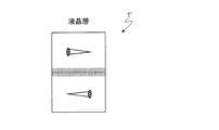
- the voltage is applied when the voltage is applied. It seems that only two liquid crystal domains are formed as in the pixel 1 ′ shown in FIG. However, for the reason described later, actually, as shown in FIG. 5C, four liquid crystal domains A, B, C, and D are formed.
- the periphery of the boundary BD1 between the first pre-tilt region 12a and the second pre-tilt region 12b of the first photo-alignment film 12 can be a defective tilt region NGR1 that cannot provide a sufficient pre-tilt angle (see FIG. 5A). Further, the periphery of the boundary BD2 between the third pre-tilt region 22a and the fourth pre-tilt region 22b of the second photo-alignment film 22 can be a defective tilt region NGR2 to which a sufficient pre-tilt angle cannot be given. However, in the liquid crystal display device 100 according to the present embodiment, as shown in FIG.
- the first pre-tilt region 12a and the second pre-tilt region 12b of the first photo-alignment film 12 are viewed from the normal direction of the display surface.
- the entire boundary BD1 and the entire boundary BD2 of the third pre-tilt region 22a and the fourth pre-tilt region 22b of the second photo-alignment film 22 overlap.
- the defective tilt region NGR1 on the first photo-alignment film 12 side and the defective tilt region NGR2 on the second photo-alignment film 22 side overlap, and as shown in FIG. A defective tilt NGR extending only in the horizontal direction is formed.
- the area of the defective tilt region NGR can be reduced as compared with the pixel 1001 shown in FIG. For this reason, it is possible to suppress a decrease in average pretilt angle in the entire pixel 1 (due to the defective tilt region NGR), so that the alignment state of the liquid crystal molecules 31 is sufficiently stabilized and a sufficient response speed is realized. be able to.
- an active matrix substrate 10 having a first photo-alignment film 12 is prepared. This step can be performed by a method similar to a method of manufacturing a general active matrix substrate for 4D-RTN mode.
- a second pretilt region 12b that defines the pretilt direction PD2 is formed by a photo-alignment process.
- This step includes, for example, a step of irradiating light to a portion to be the first pretilt region 12a in a state where the portion to be the second pretilt region 12b of the first photo-alignment film 12 is shielded by the photomask, Irradiating light to a portion to be the second pretilt region 12b in a state where the first pretilt region 12a of the first photo-alignment film 12 is shielded by the photomask.
- the light irradiation may be performed on the portion to be the second pretilt region 12b before the light irradiation is performed on the portion to be the first pretilt region 12a.
- a counter substrate 20 having a second photo-alignment film 22 is prepared separately from the active matrix substrate 10. This step can be performed by a method similar to a method for manufacturing a common counter substrate for 4D-RTN mode.
- a third pretilt region 22a that defines the third pretilt direction PD3 in a region corresponding to each of the plurality of pixels 1 of the second photoalignment film 22, and a fourth antiparallel to the third pretilt direction PD3.
- a fourth pretilt region 22b that defines the pretilt direction PD4 is formed by a photo-alignment process.
- This step includes, for example, a step of irradiating light to a portion to be the third pretilt region 22a in a state where the portion to be the fourth pretilt region 22b of the second photo-alignment film 22 is shielded by the photomask, And irradiating light onto a portion that becomes the fourth pretilt region 22b in a state where the third pretilt region 22a of the second photo-alignment film 22 is shielded by the photomask.
- the light irradiation may be performed on the portion to be the fourth pretilt region 22b before the light irradiation is performed on the portion to be the third pretilt region 22a.
- the counter substrate 20 thus bonded is bonded.
- a liquid crystal layer 30 is formed by injecting a liquid crystal material between the active matrix substrate 10 and the counter substrate 20 using, for example, a vacuum injection method.
- the liquid crystal layer 30 may be formed by a dropping method (that is, by applying a liquid crystal material on one substrate before bonding).
- the process of performing the photo-alignment process on the first photo-alignment film 12 and the process of performing the photo-alignment process on the second photo-alignment film 22 are performed in the normal direction of the display surface when the active matrix substrate 10 and the counter substrate 20 are bonded together.
- the entire boundary BD1 between the first pretilt region 12a and the second pretilt region 12b of the first photo-alignment film 12, and the entire boundary BD2 between the third pre-tilt region 22a and the fourth pretilt region 22b of the second photo-alignment film 22 are viewed. Are executed so that they overlap.
- a process of performing a realignment process including a heat process on the liquid crystal layer 30 may be performed.
- This realignment treatment can eliminate the alignment disorder (fluid alignment) that occurs when the liquid crystal material is injected.
- the liquid crystal display device 100 of the present embodiment is obtained by performing a process of attaching the pair of linearly polarizing plates 18 and 28 to the outside of the active matrix substrate 10 and the counter substrate 20.
- liquid crystal display device 100 of this embodiment when only the alignment regulating force of the first photo-alignment film 12 and the second photo-alignment film 22 is considered, only two liquid crystal domains are applied when a voltage is applied. In fact, four liquid crystal domains A, B, C and D are formed, which provides sufficiently high viewing angle characteristics. In particular, when the screen resolution is 200 ppi or more, as will be described in detail later, viewing angle characteristics substantially equivalent to those of a general 4D-RTN mode can be obtained.
- FIGS. 7A to 7D are diagrams regarding the pixel 1001 in the 4D-RTN mode
- FIGS. 8A to 8D are diagrams regarding the pixel 1 of the liquid crystal display device 100 according to the present embodiment. is there.
- FIGS. 7A to 7D are diagrams regarding the pixel 1001 in the 4D-RTN mode
- FIGS. 8A to 8D are diagrams regarding the pixel 1 of the liquid crystal display device 100 according to the present embodiment. is there.
- FIGS. 7A and 8A are calculation mask diagrams, which are defined by the pretilt directions PD1 and PD2 defined by the photo-alignment film on the active matrix substrate side and the photo-alignment film on the counter substrate side.
- the pretilt directions PD3 and PD4 are also shown.
- FIGS. 7B and 8B are diagrams showing simulation results of transmittance when a linearly polarizing plate arranged so that the transmission axes P1 and P2 are substantially orthogonal to each other is used as the polarizing plate.
- FIG.7 (c) and FIG.8 (c) are figures which show the simulation result of the transmittance
- FIG. 7D and FIG. 8D are diagrams showing the orientation distribution in the pixel, and the orientation direction of rough liquid crystal molecules (which may be called the director orientation) in each liquid crystal domain is indicated by an arrow. It is shown.
- the calculation conditions for the orientation simulation are
- the shape of the pixel electrode and the like is substantially the same in the pixel 1001 in the 4D-RTN mode and the pixel 1 of the present embodiment.
- the 4D-RTN mode pixel 1001 In the case of using the linear polarizing plate, the 4D-RTN mode pixel 1001 generates a saddle-shaped dark line characteristic of the 4D-RTN mode, as shown in FIG. 7B.
- the generation location is slightly different from the dark line of the pixel 1001 in the 4D-RTN mode, a dark line having substantially the same shape is generated. Therefore, it is considered that the 4D structure is also formed in the pixel 1 of the present embodiment.
- the liquid crystal molecules are roughly aligned in four directions in both the 4D-RTN mode pixel 1001 and the pixel 1 of the present embodiment. It was confirmed that
- the outer edge of the pixel electrode 11 includes a first edge portion 11e1 and a second edge portion 11e2.
- the first edge portion 11e1 is close to the liquid crystal domain A
- the second edge portion 11e2 is close to the liquid crystal domain C.
- the direction e1 orthogonal to the first edge portion 11e1 and going inward of the pixel electrode 11 is the direction opposite to the first pretilt direction PD1.
- a direction e2 that is orthogonal to the second edge portion 11e2 and goes inward of the pixel electrode 11 is a direction opposite to the second pretilt direction PD2.
- the outer edge of the pixel electrode 11 includes the first edge portion 11e1 and the second edge portion 11e2 as described above, four liquid crystal domains are formed when a voltage is applied. Hereinafter, this reason will be described in more detail with reference to FIGS. 10 and 11.
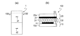
- FIG. 10A is a plan view showing one pixel 1.
- the alignment regulating force by the first photo-alignment film 12 and the second photo-alignment film 22 is indicated by solid arrows a1, a2.
- FIG. 10B is a cross-sectional view taken along the line 10B-10B 'in FIG. 10A, and shows the alignment state of the liquid crystal molecules 31 when no voltage is applied.
- the liquid crystal molecules 31 when no voltage is applied, the liquid crystal molecules 31 have a predetermined angle (pretilt) in a predetermined direction by the alignment regulating forces a1 and a2 by the first photoalignment film 12 and the second photoalignment film 22. Pretilt at (angle) ⁇ .
- the liquid crystal molecules 31 are tilted to the left with respect to the normal direction of the substrate surface.
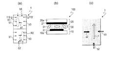
- FIG. 11A is a plan view showing one pixel 1, and FIG. 11A shows not only the alignment regulating forces a1 and a2 by the first photo-alignment film 12 and the second photo-alignment film 22, but also The alignment regulating force due to the oblique electric field generated in the vicinity of the outer edge of the pixel electrode 11 is indicated by broken arrows b1, b2, b3, and b4.
- FIG. 11B is a cross-sectional view taken along the line 11B-11B ′ in FIG. 11A, and shows the alignment state of the liquid crystal molecules 31 when a voltage is applied (however, the first photo-alignment film 12 and the second photo-alignment film 12).
- the alignment regulating forces a1 and a2 by the photo-alignment film 22 are not considered).
- FIG. 11B when a voltage is applied, the liquid crystal molecules 31 having negative dielectric anisotropy are aligned so as to be perpendicular to the electric lines of force E. Therefore, in the vicinity of the outer edge of the pixel electrode 11, there are alignment regulating forces (alignment regulating forces b1, b2, b3, and b4 shown in FIG. 11A) that tilt the liquid crystal molecules 31 toward the inside of the pixel electrode 11. To do.
- the first photo alignment film 12 and the second photo alignment film 22 are used.
- the direction of the alignment regulating force due to (which is the direction coinciding with the first pretilt direction PD1 and the second pretilt direction PD2) and the direction of the alignment regulating force due to the oblique electric field (inside the edge of the pixel electrode 11 and inside the pixel electrode 11) Is the opposite direction).
- FIG. 11C shows an enlarged lower right portion of the pixel 1.
- the liquid crystal molecules 31 are tilted upward (direction c). .
- the alignment regulating force a1 by the first photo-alignment film 12 and the second photo-alignment film 22 competes with the alignment regulating forces b1 and b4 by the oblique electric field. Falls to the side.
- the liquid crystal molecules 31 are aligned in the direction perpendicular to the display surface (approximately 270 ° direction and approximately 90 ° direction) when a voltage is applied. Oriented to Therefore, four liquid crystal domains A, B, C, and D having different director directions are formed in the pixel 1.
- liquid crystal display device 100 since the four liquid crystal domains A, B, C, and D are actually formed in each pixel 1 when a voltage is applied, sufficiently high viewing angle characteristics are obtained. It is done.
- orientation simulation and optical simulation performed at various screen resolutions (pixel pitches) will be described.
- Example 1 a liquid crystal display device having the pixel 1001 shown in FIG.
- the screen resolution and pixel pitch (pixel size) of Examples 1 to 6 and Comparative Example 1 are as shown in Table 2 below.
- a region where exposure is performed overlapping the photo-alignment film (exposure overlap region) with a width of 20 ⁇ m is formed at the center of the pixel, and the pretilt angle at the center of the exposure overlap region is 0 °. .
- the white voltage maximum gradation voltage was set to 3.9 V based on the actually measured value of the 4.18 type panel actually manufactured.
- FIGS. 12 corresponds to the first embodiment
- FIG. 13 corresponds to the second embodiment
- FIG. 14 corresponds to the third embodiment
- 15 corresponds to the fourth embodiment
- FIG. 16 corresponds to the fifth embodiment
- FIG. 17 corresponds to the sixth embodiment
- FIG. 18 corresponds to the first comparative example.
- FIG. 12 to FIG. 18 is a mask diagram for calculation.
- B in FIG. 12 to FIG. 18 is a diagram showing a simulation result of transmittance when a circularly polarizing plate is used as the polarizing plate.
- C in FIGS. 12 to 18 is a diagram showing a simulation result of transmittance when a linearly polarizing plate arranged so that the transmission axes are substantially orthogonal to each other is used as the polarizing plate.
- D in FIG. 12 to FIG. 18 is a diagram showing the orientation distribution in the pixel, and the orientation direction of rough liquid crystal molecules (which may be called the director orientation) in each liquid crystal domain is indicated by an arrow. Has been.
- E in FIG. 12 to FIG.
- FIG. 18 shows the relationship between the gradation and the luminance (luminance normalized with the luminance in the white display state set to 1), the front direction, and the right 60 ° direction (rightward viewing angle).
- FIG. 6 is a graph showing a 60 ° tilted direction and a 60 ° tilted direction (a direction in which the viewing angle is tilted 60 ° upward), and a ⁇ characteristic (luminance level) when compared to when viewed from the front direction when viewed from an oblique direction. This represents how much the key dependency shifts.
- Example 6 in which the screen resolution is the same as that of Comparative Example 1, the luminance in the observation from the right diagonal 60 ° direction and the observation from the upper diagonal 60 ° direction is shown. The difference is larger than that of Comparative Example 1.
- Example 6 Although the screen resolution of Example 6 is lower than that of Example 5, the difference in luminance between the observation from the diagonally right 60 ° direction and the observation from the diagonally upper 60 ° direction is that of Example 5. Although it is smaller than this, in Example 6, it is considered that the calculation was performed with a pattern in which the inside of the pixel was partially shielded.
- FIGS. 19A, 19B, and 19C are diagrams showing the orientation distribution in the pixels for Comparative Example 1, Example 6, and Example 2, respectively, and FIGS. ) And FIG. 13 (d) are enlarged.
- the liquid crystal molecules are in the lower left direction (approximately 225 ° direction), the lower right direction (approximately 315 ° direction), the upper right direction (approximately 45 ° direction), and the upper left direction (approximately Four regions oriented in the direction of 135 ° occupy most of the pixels.
- the region where the liquid crystal molecules are oriented in the downward direction (approximately 270 ° direction) and the upward direction (approximately 90 ° direction) is present on the upper left side and the lower right side of the pixel, small.
- the liquid crystal molecules are aligned in approximately four directions in the pixel, and the four regions in which the liquid crystal molecules are aligned in the lower left direction, the lower right direction, the upper right direction, and the upper left direction dominate in terms of optical characteristics. Is.
- Example 6 the two regions in which the liquid crystal molecules are aligned in the left direction (approximately 180 ° direction) and the right direction (approximately 0 ° direction) are the majority of the pixels. Accounted for. Although the region where the liquid crystal molecules are oriented in the downward direction (approximately 270 ° direction) and the upward direction (approximately 90 ° direction) is present on the upper left side and the lower right side of the pixel, small. Therefore, it can be considered that the liquid crystal molecules are aligned in approximately two directions within the pixel, and two regions in which the liquid crystal molecules are aligned in the left direction and the right direction are dominant in terms of optical characteristics.
- Example 2 As can be seen from FIG. 19C, the ratio of the liquid crystal molecules in the pixel aligned in the downward direction and the upward direction in the pixel is higher than that in Example 6. Therefore, it can be considered that the liquid crystal molecules are aligned in approximately four directions in the pixel, and the four regions in which the liquid crystal molecules are aligned in the downward direction, the right direction, the upward direction, and the left direction (shown in FIG. 4 and the like).
- Four liquid crystal domains A, B, C and D) dominate in terms of optical properties.
- the screen resolution is 200 ppi or more (the shorter one of the pixel pitch along the display surface horizontal direction and the pixel pitch along the display surface vertical direction is 42 ⁇ m or less)
- the difference between the liquid crystal domain with the largest area and the liquid crystal domain with the smallest area can be reduced to a certain extent (specifically, 50% or less), which is inferior to that of a general 4D-RTN mode liquid crystal display device. It was found that sufficiently high viewing angle characteristics can be obtained.
- Example 7 a liquid crystal display device 100 with a screen resolution of 217 ppi is actually manufactured as Example 7 and the results of measuring various characteristics will be described.
- a 4D-RTN mode liquid crystal display device having a screen resolution of 217 ppi was manufactured as a prototype, and as a comparative example 3, a CPA (Continuous Pinwheel Alignment) mode liquid crystal display device having a screen resolution of 217 ppi was manufactured.
- the results of measuring various characteristics will also be described.
- the CPA mode is a kind of VA mode, and is disclosed in, for example, Japanese Patent Application Laid-Open Nos. 2003-43525 and 2002-202511.
- Example 7 The results of measuring transmittance and response speed for Example 7, Comparative Example 2 and Comparative Example 3 are shown in Table 3 below.
- Table 3 As the response speed, the rising response time Tr when the display gradation is changed from 0 gradation to 32 gradation at 25 ° C. and the falling response time T d when changing the gradation from 32 gradation to 0 gradation. Is shown.
- Table 3 also shows the heat treatment temperature and the pretilt angle (average pretilt angle) in the realignment treatment step for Example 7 and Comparative Example 2.
- Example 7 two liquid crystal display devices 100 having different heat treatment temperatures were manufactured as prototypes.
- the rise response time Tr is longer in the comparative example 2 (4D-RTN mode) than the comparative example 3 (CPA mode), and is twice or more. This is considered to be caused by the fact that the average pretilt angle is reduced by increasing the ratio of the defective tilt region in the pixel as described above.
- Example 7 the rise response time substantially equivalent to that of Comparative Example 3 is realized. This is considered to be because the decrease in the average pretilt angle is suppressed as described above.
- Example 7 a higher transmittance than that of Comparative Example 3 is realized.
- an alignment regulating means (a protrusion formed from a dielectric or an opening formed in the counter electrode) is provided on the counter substrate side to stabilize the alignment by fixing the center of the axially symmetric alignment. In many cases, this orientation regulating means causes a decrease in transmittance.
- the liquid crystal display device 100 of this embodiment does not require such an alignment control means, it can implement
- Example 20 (a) and 20 (b) show the relationship between the gradation and the luminance (standardized luminance) in Example 7 and Comparative Example 2 when observed from the front direction, when observed from the 60 ° oblique direction, and It shows about the time of observation from 60 degrees up and down diagonal directions.
- FIGS. 20A and 20B in Example 7, as in Comparative Example 2, the azimuth angle dependency of the ⁇ shift was small, and sufficiently high viewing angle characteristics were obtained. Although not shown here, the same viewing angle characteristics as in Comparative Example 2 were obtained in Comparative Example 3.
- the heat treatment is preferably performed at 110 ° C. or lower.
- the nematic phase-isotropic phase transition temperature of the liquid crystal material is T NI
- the effect of the realignment treatment may not be sufficiently obtained at a temperature lower than T NI + 10 ° C. NI + 10 ° C. or higher is preferable.
- the pre-tilt angle is given by the photo-alignment film (the pre-tilt direction is defined) because the photo-functional group is formed when the photo-alignment film (typically formed from a polyimide-based material) is irradiated with ultraviolet rays. It is thought that the side chain is directed to the incident side of ultraviolet rays by the photoreaction. However, since this reaction is reversible with respect to heat, if the heat treatment in the reorientation treatment process is performed at a high temperature for a long time, the original pretilt angle (before the photoalignment treatment) (0 °: based on the substrate surface) If it does, it will return to 90 °). Therefore, it is considered preferable to perform the heat treatment at a lower temperature.
- FIGS. 21A and 21B are a cross-sectional view and a plan view schematically showing one pixel of the CPA mode liquid crystal display device 900.
- FIG. 21A and 21B are a cross-sectional view and a plan view schematically showing one pixel of the CPA mode liquid crystal display device 900.
- the liquid crystal display device 900 includes an active matrix substrate 910 and a counter substrate 920 arranged so as to face each other, and a vertical alignment type liquid crystal layer 930 provided therebetween.
- the active matrix substrate 910 includes a pixel electrode 911 provided in each pixel and a vertical alignment film 912 provided between the pixel electrode 911 and the liquid crystal layer 930.
- the pixel electrode 911 and the vertical alignment film 912 are supported by the transparent substrate 910a.
- the counter substrate 920 includes a counter electrode 921 that faces the pixel electrode 911 and a vertical alignment film 922 provided between the counter electrode 921 and the liquid crystal layer 930.
- the counter electrode 921 and the vertical alignment film 922 are supported by the transparent substrate 920a.
- the counter electrode 921 has an opening 921 a formed in a region facing substantially the center of the pixel electrode 911.
- the liquid crystal molecules 931 are axially symmetrically aligned.
- the opening 921a of the counter electrode 921 functions to fix the center of the axially symmetric orientation and stabilize the orientation.
- a protrusion sometimes referred to as a rivet
- FIG. 21C shows a simulation result of transmittance when a white voltage is applied to the liquid crystal layer 930 of the liquid crystal display device 900 (including a circularly polarizing plate as a polarizing plate). As can be seen from FIG. 21C, the region corresponding to the opening 921a of the counter electrode 921 is dark, and the luminance is lowered.
- the size of the orientation regulating means itself in the case of the opening 921a formed in the counter electrode 921, it is generally about 10 ⁇ m in diameter.
- the size of the orientation regulating means is reduced, there is a possibility that the orientation state cannot be sufficiently stabilized due to insufficient orientation regulating force.
- new equipment such as a high-resolution stepper device in order to form fine alignment regulating means.
- the size of the orientation regulating means cannot be reduced below a certain level. Therefore, when the pixel pitch is reduced with the increase in definition, the ratio of the orientation regulating means for fixing the center to the entire pixel increases.
- the CPA mode is currently often used in small and medium-sized liquid crystal display devices, but for the reasons described above, in the CPA mode liquid crystal display device, the brightness decreases as the pixel pitch decreases as the definition increases. Resulting in.
- liquid crystal display device 100 particularly when a circularly polarizing plate is used as the polarizing plate, as shown in FIG. be able to.
- the response speed is improved in the liquid crystal display device 100 according to the present embodiment because the area of the defective tilt region NGR is smaller than that in the 4D-RTN mode liquid crystal display device.
- the inventor of the present application verified whether or not the defective tilt region NGR is actually formed by the diffraction phenomenon of light, and to what extent the defective pretilt region NGR is formed if formed. The results will be explained.
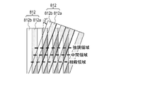
- a substrate 810 having a photo-alignment film 812 formed thereon was prepared, and the photo-alignment film 812 of the substrate 810 was irradiated with ultraviolet rays from the direction indicated by the arrow.
- FIG. 22B in a state where a partial region of the photo-alignment film 812 is shielded by the photomask in which the light shielding portions 815 are arranged in a stripe shape, the direction indicated by the arrow (FIG. 22 ( Ultraviolet rays were irradiated from the direction opposite to the direction shown in a).
- the photo-alignment film 812 is exposed to the region (first region) 812a irradiated with ultraviolet rays only once and the ultraviolet rays twice as shown in FIG.
- An irradiated region (second region) 812b was formed.
- the first region 812a is a region where a large pretilt angle (specifically, 2.5 °) can be given by ultraviolet irradiation in the first exposure step.
- the second region 812b is more strongly affected by ultraviolet irradiation in the second exposure step of the two exposure steps in which ultraviolet irradiation is performed from opposite directions, and a small pretilt angle (specifically, -0.5 °).
- the cross section of the panel obtained by bonding is configured by a region where the first regions 812a face each other and a region where the second regions 812b face each other (" A cross-section composed of only regions where the first region 812a and the second region 812b face each other (referred to as an “offset region”), and a cross-section where these regions coexist (referred to as an “intermediate region”). ) And exist.
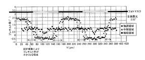
- FIG. 24 shows a position profile along the Y direction (left-right direction in FIG. 23) of the pretilt angle for each of the emphasis region, the intermediate region, and the canceling region.
- FIG. 24 also shows the positions of the light shielding part and the light transmitting part of the photomask. Note that the pretilt angle when the entire surface exposure is performed only once without a photomask is 2.55 °.
- the pretilt angle changes from 2.5 ° to ⁇ 0.5 ° in a region having a width of about 20 to 40 ⁇ m centering on the boundary between the light shielding portion and the light transmitting portion of the photomask. .
- the entire boundary BD1 between the first pretilt region 12a and the second pretilt region 12b of the first photoalignment film 12 and the third pretilt region 22a of the second photoalignment film 22 are used.
- by reducing the area of the defective tilt region NGR by overlapping the entire boundary BD2 of the fourth pretilt region 22b, it is possible to suppress a decrease in the average pretilt angle in the entire pixel 1.
- FIGS. 25A and 25B show the positions in the pixel 1 when the temperature of the heat treatment in the reorientation treatment step is 110 ° C. and 130 ° C. (both times are 40 minutes), respectively.
- 5 is a graph showing the relationship between the angle and the pretilt angle.
- shaft of the graph of Fig.25 (a) and (b) is a tilt angle with respect to a substrate surface.
- the pretilt angle was measured along the direction Y shown in FIG.
- FIG. 26 is an optical microscope image corresponding to one pixel 1.
- an area having a width of about 20 ⁇ m centered on the boundary between the pretilt areas is an area where a sufficient pretilt angle cannot be given (defective tilt area). It can be seen that the region can realize a sufficiently large pretilt angle.
- the first photo-alignment film 12 and the second photo-alignment film 22 are divided into two vertically in each pixel 1, and the first
- the first pretilt direction PD1, the second pretilt direction PD2, the third pretilt direction PD3, and the fourth pretilt direction PD4 are all substantially parallel to the left-right direction of the display surface is illustrated, but the orientation division mode is limited to the illustrated example. Not.
- the first photo-alignment film 12 and The second photo-alignment film 22 is divided into left and right parts in each pixel 1, and the first pretilt direction PD1, the second pretilt direction PD2, the third pretilt direction PD3, and the fourth pretilt direction PD4 are substantially parallel to the vertical direction of the display surface. It is good.
- one color display pixel is composed of three pixels, and the aspect ratio (aspect ratio) of one pixel is 3: 1.
- the pixels constituting one color display pixel are exemplified.
- the number and aspect ratio of the pixels are not limited to those exemplified here.
- a VA mode liquid crystal display device in which the pretilt direction of liquid crystal molecules is defined by a photo-alignment film, which is suitable for high definition.
Landscapes
- Physics & Mathematics (AREA)
- Nonlinear Science (AREA)
- Chemical & Material Sciences (AREA)
- Crystallography & Structural Chemistry (AREA)
- General Physics & Mathematics (AREA)
- Optics & Photonics (AREA)
- Mathematical Physics (AREA)
- Spectroscopy & Molecular Physics (AREA)
- Liquid Crystal (AREA)
Abstract
液晶表示装置(100)は、垂直配向型の液晶層(30)と、第1光配向膜(12)および第2光配向膜(22)とを備える。第1光配向膜は、互いに反平行なプレチルト方向(PD1、PD2)を規定する第1プレチルト領域(12a)および第2プレチルト領域(12b)を有する。第2光配向膜は、互いに反平行なプレチルト方向(PD3、PD4)を規定する第3プレチルト領域(22a)および第4プレチルト領域(22b)を有する。表示面法線方向から見たとき、第1プレチルト領域および第2プレチルト領域の境界(BD1)全体と、第3プレチルト領域および第4プレチルト領域の境界(BD2)全体とが重なっている。
Description
本発明は、液晶表示装置に関し、特に、垂直配向型の液晶層を備え、光配向膜によって液晶分子のプレチルト方向が規定される液晶表示装置に関する。また、本発明は、液晶表示装置の製造方法にも関する。
近年、液晶表示装置の表示特性が改善され、テレビジョン受像機などへの利用が進んでいる。液晶表示装置の視野角特性は向上したもののさらなる改善が望まれている。特に、垂直配向型の液晶層を用いた液晶表示装置(VAモードの液晶表示装置と呼ばれることもある。)の視野角特性を改善する要求は強い。
現在、テレビ等の大型表示装置に用いられているVAモードの液晶表示装置には、視野角特性を改善するために、1つの画素に複数の液晶ドメインを形成する配向分割構造が採用されている。配向分割構造を形成する方法としては、MVAモードが主流である。MVAモードは、例えば特許文献1に開示されている。
MVAモードでは、垂直配向型液晶層を挟んで対向する一対の基板のそれぞれの液晶層側に配向規制構造を設けることによって、各画素内に配向方向(チルト方向)が異なる複数の液晶ドメイン(典型的には配向方向は4種類)が形成される。配向規制構造としては、電極に設けたスリット(開口部)や、リブ(突起構造)が用いられ、液晶層の両側から配向規制力が発揮される。
しかしながら、スリットやリブを用いると、従来のTNモードのように配向膜によってプレチルト方向を規定した場合と異なり、スリットやリブが線状であることから、液晶分子に対する配向規制力が画素内で不均一となるため、応答速度に分布が生じるという問題がある。また、スリットやリブを設けた領域の光透過率が低下するので、表示輝度が低下するという問題もある。
上述の問題を回避するためには、VAモードの液晶表示装置についても、配向膜でプレチルト方向を規定することによって配向分割構造を形成することが好ましい。そのようにして配向分割構造が形成されたVAモードの液晶表示装置を、本願出願人は、特許文献2に提案している。
特許文献2に開示されている液晶表示装置では、配向膜でプレチルト方向を規定することによって、4分割配向構造が形成される。つまり、液晶層に電圧が印加されたときに、1つの画素内に4つの液晶ドメインが形成される。このような4分割配向構造を、単に4D構造と呼ぶこともある。
また、特許文献2に開示されている液晶表示装置では、液晶層を介して対向する一対の配向膜のうちの一方の配向膜によって規定されるプレチルト方向と、他方の配向膜によって規定されるプレチルト方向とは互いに略90°異なっている。そのため、電圧印加時には、液晶分子はツイスト配向をとる。このように、プレチルト方向(配向処理方向)が互いに直交するように設けられた一対の垂直配向膜を用いることによって液晶分子がツイスト配向をとるVAモードは、VATN(Vertical Alignment Twisted Nematic)モードあるいはRTN(Reverse Twisted Nematic)モードと呼ばれることもある。既に説明したように、特許文献2の液晶表示装置では4D構造が形成されることから、本願出願人は、特許文献2の液晶表示装置の表示モードを4D-RTNモードと呼んでいる。
液晶分子のプレチルト方向を配向膜に規定させる具体的な方法としては、特許文献2に記載されているように、光配向処理を行う方法が有望視されている。光配向処理は、非接触で処理できるので、ラビング処理のように摩擦による静電気の発生が無く、歩留まりを向上させることができる。光配向処理が施された配向膜(光配向膜)を用いたVATNモードの液晶表示装置は、特許文献3にも開示されている。
しかしながら、近年では、液晶表示装置の高精細化が進んでおり、本願発明者の検討によれば、光配向膜を用いたVATNモードを高精細な液晶表示装置に採用すると、表示(特に動画表示)に不具合が発生し得ることがわかった。具体的には、中小型用途の高精細な画素設計において、液晶分子の配向状態の安定性や、応答速度などが不十分になり得ることがわかった。
本発明は、上記問題に鑑みてなされたものであり、その目的は、光配向膜によって液晶分子のプレチルト方向が規定されるVAモードの液晶表示装置であって、高精細化に適した液晶表示装置を提供することにある。
本発明の実施形態における液晶表示装置は、互いに対向するように配置された第1基板および第2基板と、前記第1基板および前記第2基板の間に設けられた垂直配向型の液晶層とを備え、マトリクス状に配列された複数の画素を有する液晶表示装置であって、前記第1基板は、前記複数の画素のそれぞれに設けられた画素電極と、前記画素電極および前記液晶層の間に設けられた第1光配向膜とを有し、前記第2基板は、前記画素電極に対向する対向電極と、前記対向電極および前記液晶層の間に設けられた第2光配向膜とを有し、前記第1光配向膜は、前記複数の画素のそれぞれ内において、第1プレチルト方向を規定する第1プレチルト領域と、前記第1プレチルト方向に反平行な第2プレチルト方向を規定する第2プレチルト領域とを有し、前記第2光配向膜は、前記複数の画素のそれぞれ内において、第3プレチルト方向を規定する第3プレチルト領域と、前記第3プレチルト方向に反平行な第4プレチルト方向を規定する第4プレチルト領域とを有し、表示面法線方向から見たとき、前記第1光配向膜の前記第1プレチルト領域および前記第2プレチルト領域の境界全体と、前記第2光配向膜の前記第3プレチルト領域および前記第4プレチルト領域の境界全体とが重なっている。
ある実施形態において、表示面法線方向から見たとき、前記第1光配向膜の前記第1プレチルト領域と前記第2光配向膜の前記第3プレチルト領域とが重なっており、前記第1光配向膜の前記第2プレチルト領域と前記第2光配向膜の前記第4プレチルト領域とが重なっており、前記第3プレチルト方向は、前記第1プレチルト方向に反平行であり、前記第4プレチルト方向は、前記第2プレチルト方向に反平行である。
ある実施形態において、前記画素電極の外縁は、第1エッジ部および第2エッジ部を含み、前記第1エッジ部に直交し前記画素電極の内側に向かう方向は、前記第1プレチルト方向とは反対の方向であり、前記第2エッジ部に直交し前記画素電極の内側に向かう方向は、前記第2プレチルト方向とは反対の方向である。
ある実施形態において、前記画素電極と前記対向電極との間に電圧が印加されたとき、前記複数の画素のそれぞれ内において前記液晶層に4つの液晶ドメインが形成され、前記4つの液晶ドメインのそれぞれに含まれる前記液晶分子の配向方向を代表する4つのディレクタの方位は互いに異なる。
ある実施形態において、前記4つの液晶ドメインは、ディレクタの方位が第1方位である第1液晶ドメインと、第2方位である第2液晶ドメインと、第3方位である第3液晶ドメインと、第4方位である第4液晶ドメインとであって、前記第1方位、前記第2方位、前記第3方位および前記第4方位のうちの任意の2つの方位の差は90°の整数倍に略等しい。
ある実施形態において、表示面における水平方向の方位角を0°とするとき、前記第1方位は略0°、略90°、略180°または略270°である。
ある実施形態において、上述した液晶表示装置は、前記液晶層を介して互いに対向し、それぞれの透過軸が互いに略直交するように配置された一対の直線偏光板をさらに備え、前記一対の直線偏光板の前記透過軸は、前記第1プレチルト方向と略45°の角をなす。
ある実施形態において、上述した液晶表示装置は、前記液晶層を介して互いに対向する一対の円偏光板をさらに備える。
ある実施形態において、前記液晶層は、負の誘電異方性を有する液晶分子を含む。
ある実施形態において、表示面水平方向に沿った画素ピッチおよび表示面垂直方向に沿った画素ピッチのうちの短い方の画素ピッチは42μm以下である。
ある実施形態において、画面解像度は200ppi以上である。
本発明の実施形態における液晶表示装置の製造方法は、互いに対向するように配置された第1基板および第2基板と、前記第1基板および前記第2基板の間に設けられた垂直配向型の液晶層とを備え、マトリクス状に配列された複数の画素を有し、前記第1基板は、前記複数の画素のそれぞれに設けられた画素電極と、前記画素電極および前記液晶層の間に設けられた第1光配向膜とを有し、前記第2基板は、前記画素電極に対向する対向電極と、前記対向電極および前記液晶層の間に設けられた第2光配向膜とを有する液晶表示装置の製造方法であって、前記第1光配向膜の、前記複数の画素のそれぞれに対応する領域内に、第1プレチルト方向を規定する第1プレチルト領域と、前記第1プレチルト方向に反平行な第2プレチルト方向を規定する第2プレチルト領域とを光配向処理によって形成する工程(A)と、前記第2光配向膜の、前記複数の画素のそれぞれに対応する領域内に、第3プレチルト方向を規定する第3プレチルト領域と、前記第3プレチルト方向に反平行な第4プレチルト方向を規定する第4プレチルト領域とを光配向処理によって形成する工程(B)と、前記工程(A)および前記工程(B)の後に、前記第1基板と前記第2基板とを貼り合わせる工程(C)と、を包含し、前記工程(A)および前記工程(B)は、前記工程(C)において前記第1基板と前記第2基板とを貼り合わせたときに、表示面法線方向から見て、前記第1光配向膜の前記第1プレチルト領域および前記第2プレチルト領域の境界全体と、前記第2光配向膜の前記第3プレチルト領域および前記第4プレチルト領域の境界全体とが重なるように実行される。
ある実施形態において、上述した液晶表示装置の製造方法は、前記工程(C)の後に、前記液晶層に加熱処理を含む再配向処理を施す工程(D)をさらに包含し、前記加熱処理は、110℃以下で行われる。
本発明の実施形態によると、光配向膜によって液晶分子のプレチルト方向が規定されるVAモードの液晶表示装置であって、高精細化に適した液晶表示装置が提供される。
以下、図面を参照しながら本発明の実施形態を説明する。なお、本発明は以下の実施形態に限定されるものではない。
図1に、本実施形態における液晶表示装置100を示す。図1は、液晶表示装置100を模式的に示す断面図である。
液晶表示装置100は、図1に示すように、互いに対向するように配置されたアクティブマトリクス基板(第1基板)10および対向基板(第2基板)20と、アクティブマトリクス基板10および対向基板20の間に設けられた液晶層30とを備える。液晶表示装置100は、さらに、マトリクス状に配列された複数の画素を有する。典型的には、複数の画素は、赤を表示する赤画素、緑を表示する緑画素および青を表示する青画素を含み、赤画素、緑画素および青画素の3つの画素によって1つのカラー表示画素が構成される。
アクティブマトリクス基板(「TFT基板」とも呼ばれる)10は、複数の画素のそれぞれに設けられた画素電極11と、画素電極11および液晶層30の間に設けられた第1光配向膜12とを有する。画素電極11および第1光配向膜12は、絶縁性を有する透明基板(例えばガラス基板)10aによって支持されている。また、ここでは図示していないが、アクティブマトリクス基板は、画素電極11に電気的に接続された薄膜トランジスタ(TFT)や、TFTに走査信号を供給する走査配線(ゲートバスライン)、TFTに表示信号を供給する信号配線(ソースバスライン)などを有する。
対向基板(「カラーフィルタ基板」とも呼ばれる。)20は、画素電極11に対向する対向電極21と、対向電極21および液晶層30の間に設けられた第2光配向膜22とを有する。対向電極21および第2光配向膜22は、絶縁性を有する透明基板(例えばガラス基板)20aによって支持されている。また、ここでは図示していないが、対向基板20は、カラーフィルタ層を有する。典型的には、カラーフィルタ層は、赤画素に対応して設けられた赤カラーフィルタ、緑画素に対応して設けられた緑カラーフィルタおよび青画素に対応して設けられた青カラーフィルタを含む。
液晶層30は、負の誘電異方性を有する液晶分子31を含む、垂直配向型の液晶層である。液晶層30に電圧が印加されていない状態において、液晶分子31は、図1に示されているように、基板面に対して略垂直に配向している。
液晶表示装置100は、さらに、少なくとも液晶層30を介して互いに対向する一対の直線偏光板18および28を備える。直線偏光板18および28は、それぞれの透過軸が互いに略直交するように配置されている。つまり、直線偏光板18および28は、クロスニコルに配置されている。なお、一対の直線偏光板18および28に代えて、一対の円偏光板を設けてもよい。つまり、液晶層30に入射する光は、直線偏光であってもよいし、円偏光であってもよい。
第1光配向膜12および第2光配向膜22のそれぞれは、光配向処理が施された垂直配向膜であり、液晶分子31のプレチルト方向を規定する。第1光配向膜12は、各画素内において、互いに異なるプレチルト方向を規定する2つの領域を有する。同様に、第2光配向膜22は、各画素内において、互いに異なるプレチルト方向を規定する2つの領域を有する。
以下、本実施形態の液晶表示装置100において第1光配向膜12および第2光配向膜22によって形成される配向分割構造を説明するが、それに先立ち、特許文献2や特許文献3に開示されているような4D-RTNモードにおける配向分割構造を説明する。
図2に、一般的な4D-RTNモードの液晶表示装置における画素1001の配向分割構造を示す。液晶層に電圧が印加されている状態において、画素1001には、図2に示すように、4つの液晶ドメインA、B、CおよびDが形成される。4つの液晶ドメインA、B、CおよびDは、2行2列のマトリクス状に配置されている。
液晶ドメインA、B、CおよびDのディレクタt1、t2、t3およびt4の方位は、任意の2つの方向の差が90°の整数倍に略等しい4つの方位である。ディレクタt1、t2、t3およびt4は、各液晶ドメインに含まれる液晶分子の配向方向を代表するものであり、4D-RTNモードでは、液晶層に電圧が印加されたときの液晶層の層面内および厚さ方向における中央付近の液晶分子のチルト方向である。各液晶ドメインは、ディレクタの方位(上述したチルト方向)に特徴付けられ、このディレクタの方位が各ドメインの視角依存性に支配的な影響を与える。
なお、ここで、液晶層を介して互いに対向する一対の偏光板は、透過軸(偏光軸)が互いに直交するように配置されており、より具体的には、一方の透過軸が表示面の水平方向に平行で、他方の透過軸が表示面の垂直方向に平行となるように配置されている。
表示面における水平方向の方位角(3時方向)を0°とすると、液晶ドメインAのディレクタt1の方位は略225°方向、液晶ドメインBのディレクタt2の方位は略315°方向、液晶ドメインCのディレクタt3の方位は略45°方向、液晶ドメインDのディレクタt4の方位は略135°方向である。つまり、液晶ドメインA、B、CおよびDは、それぞれのディレクタの方位が、隣接する液晶ドメイン間で略90°異なるように配置されている。
ここで、図3(a)、(b)および(c)を参照しながら、図2に示した画素1001の配向分割構造を得るための配向分割方法を説明する。図3(a)は、アクティブマトリクス基板に設けられている光配向膜によって規定されるプレチルト方向PD1およびPD2を示し、図3(b)は、対向基板に設けられている光配向膜によって規定されるプレチルト方向PD3およびPD4を示している。また、図3(c)は、液晶層に電圧を印加したときのチルト方向(ディレクタ)を示している。
アクティブマトリクス基板側の領域(1つの画素1001に対応する領域)は、図3(a)に示すように、左右に2分割されており、それぞれの領域(左側領域と右側領域)の光配向膜(垂直配向膜)が互いに反平行なプレチルト方向PD1およびPD2を規定するように光配向処理が行われている。ここでは、矢印で示した方向から紫外線を斜め照射することによって光配向処理が行われている。
一方、対向基板側の領域(1つの画素領域1001に対応する領域)は、図3(b)に示すように、上下に2分割されており、それぞれの領域(上側領域と下側領域)の光配向膜(垂直配向膜)が互いに反平行なプレチルト方向PD3およびPD4を規定するように光配向処理が行われている。ここでは、矢印で示した方向から紫外線を斜め照射することによって光配向処理が行われている。
図3(a)および(b)に示したように光配向処理がなされたアクティブマトリクス基板および対向基板を貼り合わせることによって、図3(c)に示すように配向分割された画素1001を形成することができる。図3(a)、(b)および(c)からわかるように、液晶ドメインA~Dのそれぞれについて、アクティブマトリクス基板の光配向膜によって規定されるプレチルト方向と、対向基板の光配向膜によって規定されるプレチルト方向とは互いに略90°異なっており、これら2つのプレチルト方向の中間の方向にチルト方向(各液晶ドメインのディレクタの方位)が規定される。
既に説明したように、画素1001のような(つまり一般的な4D-RTNモードの)配向分割構造を高精細な液晶表示装置に採用すると、表示(特に動画表示)に不具合が発生することがある。以下、この理由を説明する。
4D-RTNモードの配向分割構造を形成する場合、アクティブマトリクス側の光配向膜および対向基板側の光配向膜のそれぞれについて、2回ずつ露光工程を実行する必要がある。1回目の露光工程と、2回目の露光工程とで、紫外線の照射は異なる方向から行われる。フォトマスクを用いた走査露光により上述した露光工程を行う場合、光の回折現象により、露光の継ぎ目(規定するプレチルト方向が異なる2つの領域の境界)の周辺は、十分なプレチルト角を付与できない領域(以下では「不良チルト領域」と呼ぶ。)となる。なお、本願明細書では、「プレチルト角」は、電圧無印加時において液晶分子31の長軸が基板面法線方向に対してなす角を指す。
具体的には、アクティブマトリクス基板側の光配向膜では、図3(a)に示すように、左側領域と右側領域との境界BD1の周辺が不良チルト領域NGR1となる。また、対向基板側の光配向膜では、図3(b)に示すように、上側領域と下側領域との境界BD2と周辺が不良チルト領域NGR2となる。そのため、アクティブマトリクス基板と対向基板とを貼り合わせると、各画素1001において、垂直方向に延びる部分(不良チルト領域NGR1に対応)と水平方向に延びる部分(不良チルト領域NGR2に対応)とを含む、十字形状の不良チルト領域NGRが形成される。
中小型用途の高精細な画素設計では、画素ピッチが小さいので、画素1001全体に占める不良プレチルト領域の割合が大きくなる。そのため、画素1001全体での平均的なプレチルト角が小さくなってしまい、そのことによって、液晶分子の配向状態が不安定になったり、応答速度が低下したり(つまり応答時間が長くなったり)する。
続いて、本実施形態の液晶表示装置100における画素の配向分割構造を説明する。図4に、液晶表示装置100における画素1の配向分割構造を示す。
画素電極11と対向電極21との間に電圧が印加されたとき、各画素1内において、図4に示すように、液晶層30に4つの液晶ドメインA、B、CおよびDが形成される。これら4つの液晶ドメインA、B、CおよびDのそれぞれに含まれる液晶分子31の配向方向を代表する4つのディレクタt1、t2、t3およびt4の方位は、互いに異なる。
表示面における水平方向の方位角(3時方向)を0°とすると、液晶ドメインAのディレクタt1の方位は略270°方向、液晶ドメインBのディレクタt2の方位は略0°方向、液晶ドメインCのディレクタt3の方位は略90°方向、液晶ドメインDのディレクタt4の方位は略180°方向である。つまり、液晶ドメインA、B、CおよびDの4つのディレクタの方位のうちの任意の2つの方位の差は、90°の整数倍に略等しい。
一対の直線偏光板18および28の透過軸(偏光軸)P1およびP2は、液晶ドメインA、B、CおよびDのディレクタt1、t2、t3およびt4の方位と略45°の角をなす。また、後の説明からもわかるように、一対の直線偏光板18および28の透過軸P1およびP2は、第1光配向膜12および第2光配向膜22によって規定されるプレチルト方向とも略45°の角をなす。
なお、図4には、4つの液晶ドメインA、B、CおよびDの画素1内に占める面積が互いに等しい場合を例示しているが、4つの液晶ドメインA、B、CおよびDの面積は互いに等しくなくてもよい。ただし、視野角特性の均一さの観点からは、4つの液晶ドメインA、B、CおよびDの面積の差がなるべく小さいことが好ましく、具体的には、4つの液晶ドメインA、B、CおよびDの内の最大の液晶ドメインの面積と最小の液晶ドメインの面積との差が、最大の面積の50%以下であることが好ましい。図4に示す例は、視野角特性上最も好ましい(つまり理想的な)4分割構造の例である。
続いて、図5(a)、(b)および(c)を参照しながら、本実施形態における液晶表示装置100の画素1の配向分割構造を得るための配向分割方法を説明する。図5(a)は、アクティブマトリクス基板10に設けられている第1光配向膜12によって規定されるプレチルト方向PD1およびPD2を示し、図5(b)は、対向基板20に設けられている第2光配向膜22によって規定されるプレチルト方向PD3およびPD4を示している。また、図5(c)は、液晶層30に電圧を印加したときのチルト方向(ディレクタ)を示している。
第1光配向膜12は、各画素1内において、図5(a)に示すように、第1プレチルト方向PD1を規定する第1プレチルト領域12aと、第1プレチルト方向PD1に反平行な第2プレチルト方向PD2を規定する第2プレチルト領域12bとを有する。具体的には、第1光配向膜12の1つの画素1に対応する領域は、上下に2分割されており、それぞれの領域(第1プレチルト領域および第2プレチルト領域)12a、12bが互いに反平行なプレチルト方向(第1プレチルト方向および第2プレチルト方向)PD1およびPD2を規定するように光配向処理が行われている。ここでは、光配向処理は、矢印で示した方向から紫外線を斜め照射することによって行われている。
一方、第2光配向膜22は、各画素1内において、図5(b)に示すように、第3プレチルト方向PD3を規定する第3プレチルト領域22aと、第3プレチルト方向PD3に反平行な第4プレチルト方向PD4を規定する第4プレチルト領域22bとを有する。具体的には、第2光配向膜22の1つの画素1に対応する領域は、上下に2分割されており、それぞれの領域(第3プレチルト領域および第4プレチルト領域)22a、22bが互いに反平行なプレチルト方向(第3プレチルト方向および第4プレチルト方向)PD3およびPD4を規定するように光配向処理が行われている。ここでは、光配向処理は、矢印で示した方向から紫外線を斜め照射することによって行われている。なお、アクティブマトリクス基板10および対向基板20を貼り合わせた状態において、表示面法線方向から見たとき、第2光配向膜22の第3プレチルト領域22aは、第1光配向膜12の第1プレチルト領域12aに重なり(対向し)、第2光配向膜22の第4プレチルト領域22bは第1光配向膜12の第2プレチルト領域12bに重なる(対向する)。また、アクティブマトリクス基板10および対向基板20を貼り合わせた状態において、第3プレチルト方向PD3は、第1プレチルト方向PD1に反平行であり、第4プレチルト方向PD4は、第2プレチルト方向PD2に反平行である。
図5(a)および(b)に示したように光配向処理がなされたアクティブマトリクス基板10および対向基板20を貼り合わせることによって、図5(c)に示すように配向分割された画素1を形成することができる。なお、図5(a)および(b)に示したように光配向処理がなされた第1光配向膜12および第2光配向膜22の配向規制力のみを考慮した場合、電圧印加時には、図6に示す画素1’のように、2つの液晶ドメインのみが形成されるようにも思われる。しかしながら、後述する理由から、実際には、図5(c)に示したように、4つの液晶ドメインA、B、CおよびDが形成される。
第1光配向膜12の第1プレチルト領域12aと第2プレチルト領域12bとの境界BD1の周辺は、十分なプレチルト角を付与できない不良チルト領域NGR1となり得る(図5(a)参照)。また、第2光配向膜22の第3プレチルト領域22aと第4プレチルト領域22bとの境界BD2の周辺は、十分なプレチルト角を付与できない不良チルト領域NGR2となり得る。しかしながら、本実施形態における液晶表示装置100では、図5(c)に示すように、表示面法線方向から見たとき、第1光配向膜12の第1プレチルト領域12aおよび第2プレチルト領域12bの境界BD1全体と、第2光配向膜22の第3プレチルト領域22aおよび第4プレチルト領域22bの境界BD2全体とが重なっている。そのため、第1光配向膜12側の不良チルト領域NGR1と、第2光配向膜22側の不良チルト領域NGR2とが重なることになり、図5(c)に示すように、画素1全体では、水平方向にのみ延びる不良チルトNGRが形成される。
従って、本実施形態における液晶表示装置100の画素1では、図3(c)に示した画素1001に比べ、不良チルト領域NGRの面積を小さくすることができる。そのため、画素1全体での平均的なプレチルト角の低下(不良チルト領域NGRに起因する)を抑制できるので、液晶分子31の配向状態を十分に安定化させ、また、十分な応答速度を実現することができる。
ここで、本実施形態における液晶表示装置100の製造方法を説明する。
まず、第1光配向膜12を有するアクティブマトリクス基板10を用意する。この工程は、一般的な4D-RTNモード用のアクティブマトリクス基板を作製する手法と同様の手法により実行され得る。
次に、第1光配向膜12の、複数の画素1のそれぞれに対応する領域内に、第1プレチルト方向PD1を規定する第1プレチルト領域12aと、第1プレチルト方向PD1に反平行な第2プレチルト方向PD2を規定する第2プレチルト領域12bとを光配向処理によって形成する。この工程は、例えば、第1光配向膜12の第2プレチルト領域12bとなる部分がフォトマスクによって遮光された状態で、第1プレチルト領域12aとなる部分に光を照射する工程と、その後に、第1光配向膜12の第1プレチルト領域12aがフォトマスクによって遮光された状態で、第2プレチルト領域12bとなる部分に光を照射する工程とを含む。なお、第1プレチルト領域12aとなる部分に光照射を行うのよりも前に、第2プレチルト領域12bとなる部分に光照射を行ってもよいことは言うまでもない。
一方、アクティブマトリクス基板10とは別途に、第2光配向膜22を有する対向基板20を用意する。この工程は、一般的な4D-RTNモード用の対向基板を作製する手法と同様の手法により実行され得る。
次に、第2光配向膜22の、複数の画素1のそれぞれに対応する領域内に、第3プレチルト方向PD3を規定する第3プレチルト領域22aと、第3プレチルト方向PD3に反平行な第4プレチルト方向PD4を規定する第4プレチルト領域22bとを光配向処理によって形成する。この工程は、例えば、第2光配向膜22の第4プレチルト領域22bとなる部分がフォトマスクによって遮光された状態で、第3プレチルト領域22aとなる部分に光を照射する工程と、その後に、第2光配向膜22の第3プレチルト領域22aがフォトマスクによって遮光された状態で、第4プレチルト領域22bとなる部分に光を照射する工程とを含む。なお、第3プレチルト領域22aとなる部分に光照射を行うのよりも前に、第4プレチルト領域22bとなる部分に光照射を行ってもよいことは言うまでもない。
その後、第1光配向膜12に第1プレチルト領域12aおよび第2プレチルト領域12bが形成されたアクティブマトリクス基板10と、第2光配向膜22に第3プレチルト領域22aおよび第4プレチルト領域22bが形成された対向基板20とを貼り合わせる。
続いて、アクティブマトリクス基板10と対向基板20との間に例えば真空注入法を用いて液晶材料を注入することにより、液晶層30を形成する。なお、滴下法により(つまり貼り合わせ前に一方の基板上に液晶材料を付与しておくことにより)液晶層30を形成してもよいことは言うまでもない。
第1光配向膜12に光配向処理を行う工程および第2光配向膜22に光配向処理を行う工程は、アクティブマトリクス基板10と対向基板20とを貼り合わせたときに、表示面法線方向から見て、第1光配向膜12の第1プレチルト領域12aおよび第2プレチルト領域12bの境界BD1全体と、第2光配向膜22の第3プレチルト領域22aおよび第4プレチルト領域22bの境界BD2全体とが重なるように実行される。
なお、アクティブマトリクス基板10と対向基板20とを貼り合わせる工程の後に、液晶層30に加熱処理を含む再配向処理を施す工程を行ってもよい。この再配向処理により、液晶材料の注入時に発生する配向の乱れ(流動配向)をなくすことができる。
その後、一対の直線偏光板18および28をアクティブマトリクス基板10および対向基板20の外側に貼り付ける工程等を行うことにより、本実施形態の液晶表示装置100が得られる。
なお、既に説明したように、本実施形態の液晶表示装置100では、第1光配向膜12および第2光配向膜22の配向規制力のみを考慮した場合、電圧印加時には、2つの液晶ドメインのみが形成されるはずであるにも関わらず、実際には、4つの液晶ドメインA、B、CおよびDが形成され、そのことによって十分に高い視野角特性が得られる。特に、画面解像度が200ppi以上であると、後に詳述するように、一般的な4D-RTNモードとほぼ同等の視野角特性が得られる。
ここで、図7および図8を参照しながら、一般的な4D-RTNモードの画素1001および本実施形態における液晶表示装置100の画素1のそれぞれについて、電圧印加時の液晶分子の配向状態を検証するために配向シミュレーションを行った結果を説明する。図7(a)~(d)は、4D-RTNモードの画素1001についての図であり、図8(a)~(d)は、本実施形態における液晶表示装置100の画素1についての図である。図7(a)および図8(a)は、計算用のマスク図であり、アクティブマトリクス基板側の光配向膜によって規定されるプレチルト方向PD1およびPD2と、対向基板側の光配向膜によって規定されるプレチルト方向PD3およびPD4とが併せて示されている。図7(b)および図8(b)は、偏光板として透過軸P1およびP2が略直交するように配置された直線偏光板が用いられるときの透過率のシミュレーション結果を示す図である。図7(c)および図8(c)は、偏光板として円偏光板が用いられるときの透過率のシミュレーション結果を示す図である。図7(d)および図8(d)は、画素内の配向分布を示す図であり、各液晶ドメインにおけるおおまかな液晶分子の配向方向(ディレクタの方位といってもよい)が矢印で併せて示されている。なお、配向シミュレーションに際しての計算条件は、下記表1に示す通りである。

図7(a)および図8(a)からわかるように、4D-RTNモードの画素1001と、本実施形態の画素1とで、画素電極等の形状はほぼ同じである。
円偏光板を用いる場合、図7(c)および図8(c)に示すように、4D-RTNモードの画素1001および本実施形態の画素1のいずれについても、画素の中央に小さな暗点が存在するものの、画素の他の領域では高い輝度が得られている。
直線偏光板を用いる場合、4D-RTNモードの画素1001では、図7(b)に示すように、4D-RTNモードに特徴的な卍形状の暗線が発生する。一方、本実施形態の画素1では、図8(b)に示すように、4D-RTNモードの画素1001の暗線とは発生箇所がやや異なるものの、ほぼ同じ形状の暗線が発生する。従って、本実施形態の画素1についても、4D構造が形成されていると考えられる。
また、図7(d)および図8(d)からわかるように、4D-RTNモードの画素1001および本実施形態の画素1のいずれについても、おおまかには4つの方向に液晶分子が配向していることが確認された。
続いて、図9を参照しながら、本実施形態の画素1において4つの液晶ドメインが形成される理由を説明する。
図9に示すように、本実施形態の画素1では、画素電極11の外縁は、第1エッジ部11e1および第2エッジ部11e2を含む。第1エッジ部11e1は、液晶ドメインAに近接しており、第2エッジ部11e2は、液晶ドメインCに近接している。
第1エッジ部11e1に直交し画素電極11の内側に向かう方向e1は、第1プレチルト方向PD1とは反対の方向である。また、第2エッジ部11e2に直交し画素電極11の内側に向かう方向e2は、第2プレチルト方向PD2とは反対の方向である。
画素電極11の外縁が上述したような第1エッジ部11e1および第2エッジ部11e2を含んでいることにより、電圧印加時に4つの液晶ドメインが形成される。以下、図10および図11を参照しながら、この理由をより詳細に説明する。
図10(a)は、1つの画素1を示す平面図であり、図10(a)には、第1光配向膜12および第2光配向膜22による配向規制力が実線の矢印a1、a2で示されている。また、図10(b)は、図10(a)中の10B-10B’線に沿った断面図であり、電圧無印加時における液晶分子31の配向状態が示されている。図10(b)からわかるように、電圧無印加時には、第1光配向膜12および第2光配向膜22による配向規制力a1、a2によって、液晶分子31は所定の方向に所定の角度(プレチルト角)θでプレチルトしている。例えば画素1の上側では、液晶分子31は、基板面法線方向に対して左側にチルトしている。
図11(a)は、1つの画素1を示す平面図であり、図11(a)には、第1光配向膜12および第2光配向膜22による配向規制力a1、a2だけでなく、画素電極11の外縁近傍に生成される斜め電界による配向規制力が破線の矢印b1、b2、b3、b4で示されている。また、図11(b)は、図11(a)中の11B-11B’線に沿った断面図であり、電圧印加時における液晶分子31の配向状態(ただし第1光配向膜12および第2光配向膜22による配向規制力a1、a2は考慮されていない)が示されている。図11(b)からわかるように、電圧印加時には、負の誘電異方性を有する液晶分子31は、電気力線Eに垂直になるように配向する。そのため、画素電極11の外縁近傍では、画素電極11の内側に向けて液晶分子31を倒すような配向規制力(図11(a)中に示す配向規制力b1、b2、b3、b4)が存在する。
そのため、画素1の一部(ここでは画素1の左上部分と右下部分であり、図11(a)中に示す領域R1およびR2)では、第1光配向膜12および第2光配向膜22による配向規制力の方向(第1プレチルト方向PD1および第2プレチルト方向PD2と一致する方向である)と、斜め電界による配向規制力の方向(画素電極11のエッジ部に直交し画素電極11の内側に向かう方向である)とが反対となる。図11(c)は、画素1の右下部分を拡大して示している。この部分では、第1光配向膜12および第2光配向膜22による配向規制力a2と、斜め電界による配向規制力b2およびb3とが競合する結果、液晶分子31は上側(方向c)に倒れる。同様に、画素1の左上部分では、第1光配向膜12および第2光配向膜22による配向規制力a1と、斜め電界による配向規制力b1およびb4とが競合する結果、液晶分子31は下側に倒れる。
上述したメカニズムにより、第1エッジ部11e1および第2エッジ部11e2に近接する液晶ドメインAおよびCでは、電圧印加時に、液晶分子31は、表示面垂直方向(略270°方向および略90°方向)に配向する。そのため、画素1内には、ディレクタの方位が互いに異なる4つの液晶ドメインA、B、CおよびDが形成される。
このように、本実施形態における液晶表示装置100では、電圧印加時に各画素1内において実際には4つの液晶ドメインA、B、CおよびDが形成されるので、十分に高い視野角特性が得られる。ここで、本実施形態における液晶表示装置100の視野角特性を検証するために、様々な画面解像度(画素ピッチ)で配向シミュレーションおよび光学シミュレーションを行った結果を説明する。
シミュレーションは、実施例1~6として6つの画面解像度について行った。また、比較例1として、図2に示した画素1001を有する液晶表示装置についてもシミュレーションを行った。実施例1~6および比較例1の画面解像度および画素ピッチ(画素サイズ)は、下記表2に示す通りである。また、シミュレーションに際しては、液晶材料を屈折率異方性Δn=0.1199のネマチック液晶材料とし、液晶層の厚さ(セル厚)を3.1μmとする条件で行った。さらに、隣接する画素電極同士の間隔は6μmとし、プレチルト角は2.4°とした。また、画素の中央部分に、光配向膜に対して重複して露光が行われる領域(露光重複領域)が幅20μmで形成されるものとし、露光重複領域の中心におけるプレチルト角は0°とした。白電圧(最高階調電圧)は、実際に試作した4.18型パネルの実測値に基づいて3.9Vに設定した。
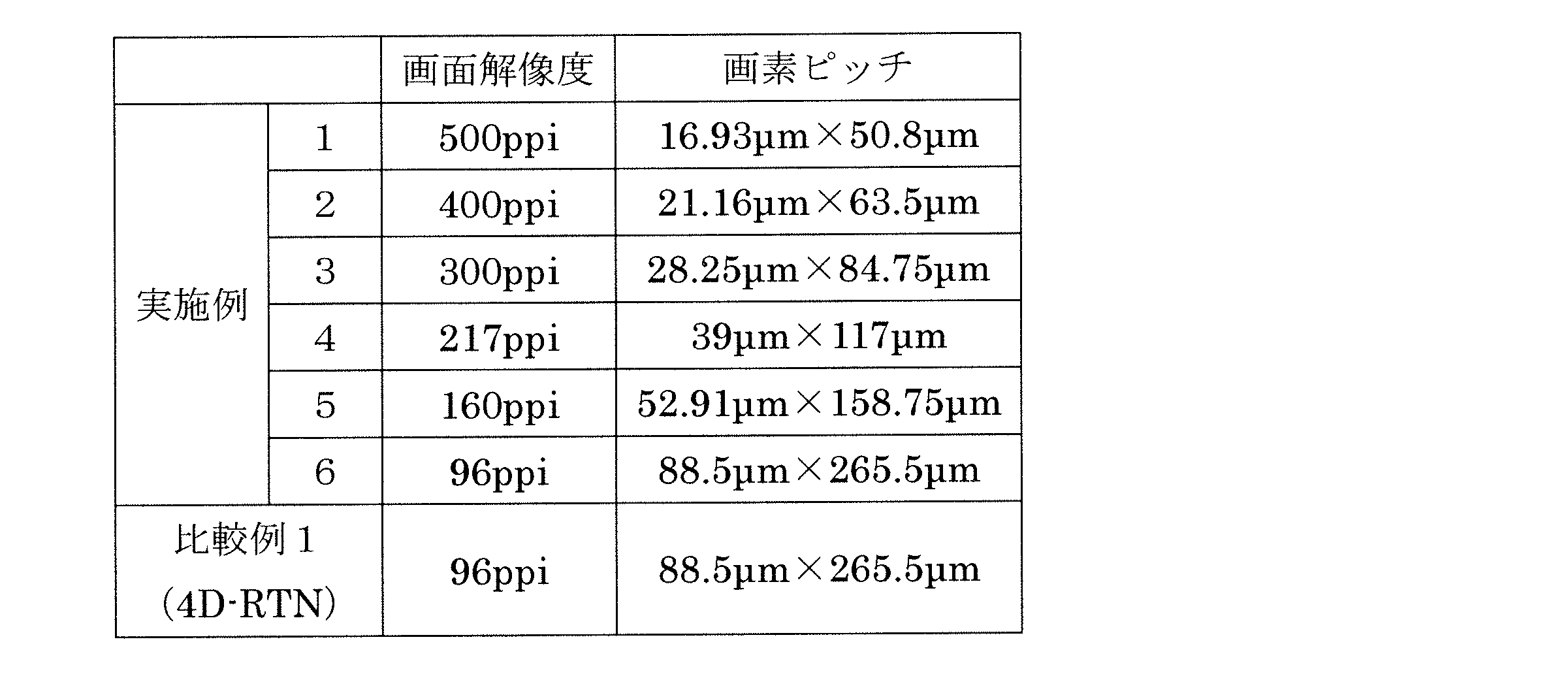
図12~図18を参照しながら、実施例1~6および比較例1についてのシミュレーション結果を説明する。図12は実施例1に対応し、図13は実施例2に対応し、図14は実施例3に対応している。また、図15は実施例4に対応し、図16は実施例5に対応し、図17は実施例6に対応し、図18は比較例1に対応している。
図12~図18中の(a)は、計算用のマスク図である。図12~図18中の(b)は、偏光板として円偏光板が用いられるときの透過率のシミュレーション結果を示す図である。図12~図18中の(c)は、偏光板として透過軸が略直交するように配置された直線偏光板が用いられるときの透過率のシミュレーション結果を示す図である。図12~図18中の(d)は、画素内の配向分布を示す図であり、各液晶ドメインにおけるおおまかな液晶分子の配向方向(ディレクタの方位といってもよい)が矢印で併せて示されている。図12~図18中の(e)は、階調と輝度(白表示状態における輝度を1として規格化された輝度)との関係を、正面方向、右斜め60°方向(右方向に視角を60°倒した方向)、上斜め60°方向(上方向に視角を60°倒した方向)について示すグラフであり、斜め方向からの観察時に正面方向からの観察時に比べてγ特性(輝度の階調依存性)がどれだけシフトするかを表している。以下の説明では、特に、図12~図18中の(e)に注目されたい。
図18からわかるように、比較例1(一般的な4D-RTNモード)では、画面解像度が比較的低い(96ppi、画素ピッチは88.5μm×265.5μm)にもかかわらず、右斜め60°方向からの観察時と上斜め60°方向からの観察時とで、ほぼすべての階調について輝度の差がほとんどない。これは、良好な視野角特性が得られていること、つまり、斜め方向からの観察時のγ特性のシフト(γシフト)の方位角依存性が小さいことを示している。
これに対し、図17からわかるように、比較例1と画面解像度が同じである実施例6では、右斜め60°方向からの観察時と上斜め60°方向からの観察時とでの輝度の差が、比較例1に比べると大きい。
また、図12~図17からわかるように、実施例1~6では、画面解像度が高くなるほど(画素ピッチが小さくなるほど)、右斜め60°方向からの観察時と上斜め60°方向からの観察時とでの輝度の差が小さくなる傾向がある。そして、画面精細度が200ppi以上(実施例1~4)になると、γシフトの方位角依存性が十分に小さくなり、十分に高い視野角特性が得られることがわかる。
なお、実施例6は、実施例5よりも画面解像度が低いにも関わらず、右斜め60°方向からの観察時と上斜め60°方向からの観察時とでの輝度の差が実施例5よりも小さいが、これは、実施例6については、画素内を部分的に遮光したパターンで計算したためであると考えられる。
続いて、図19(a)、(b)および(c)を参照しながら、画面解像度が高くなるほど高い視野角特性が得られる理由を説明する。図19(a)、(b)および(c)は、それぞれ比較例1、実施例6および実施例2についての画素内の配向分布を示す図であり、図18(d)、図17(d)および図13(d)を拡大したものである。
比較例1では、図19(a)からわかるように、液晶分子が左下方向(略225°方向)、右下方向(略315°方向)、右上方向(略45°方向)、左上方向(略135°方向)に配向している4つの領域が画素の大部分を占めている。液晶分子が下方向(略270°方向)および上方向(略90°方向)に配向している領域が画素の左上側および右下側に存在しているものの、それらが画素内に占める割合は小さい。そのため、画素内では液晶分子はおおよそ4方向に配向しているとみなすことができ、液晶分子が左下方向、右下方向、右上方向、左上方向に配向している4つの領域が光学特性に関して支配的である。
一方、実施例6では、図19(b)からわかるように、液晶分子が左方向(略180°方向)、右方向(略0°方向)に配向している2つの領域が画素の大部分を占めている。液晶分子が下方向(略270°方向)および上方向(略90°方向)に配向している領域が画素の左上側および右下側に存在しているものの、それらが画素内に占める割合は小さい。そのため、画素内では液晶分子はおおよそ2方向に配向しているとみなすことができ、液晶分子が左方向、右方向に配向している2つの領域が光学特性に関して支配的である。
これに対し、実施例2では、図19(c)からわかるように、液晶分子が下方向、上方向に配向している領域の画素内で占める割合が、実施例6においてよりも高くなる。そのため、画素内では液晶分子はおおよそ4方向に配向しているとみなすことができ、液晶分子が下方向、右方向、上方向、左方向に配向している4つの領域(図4などに示した4つの液晶ドメインA、B、CおよびD)が光学特性に関して支配的となる。
上述したように、画面解像度が高くなるほど(つまり画素ピッチが小さくなるほど)、4つの液晶ドメインの面積差が小さくなり、視野角特性が向上する。本願発明者の検討によれば、画面解像度が200ppi以上である(表示面水平方向に沿った画素ピッチおよび表示面垂直方向に沿った画素ピッチのうちの短い方の画素ピッチが42μm以下である)ことにより、面積が最大の液晶ドメインと面積が最少の液晶ドメインとの差をある程度小さく(具体的には50%以下)とすることができ、一般的な4D-RTNモードの液晶表示装置と遜色のない、十分に高い視野角特性が得られることがわかった。
続いて、実施例7として画面解像度が217ppiの液晶表示装置100を実際に試作し、各種特性を測定した結果を説明する。また、比較例2として画面解像度が217ppiの4D-RTNモードの液晶表示装置を試作するとともに、比較例3として画面解像度が217ppiのCPA(Continuous Pinwheel Alignment)モードの液晶表示装置を試作し、これらについて各種特性を測定した結果も併せて説明する。なお、CPAモードは、VAモードの一種であり、例えば特開2003-43525号公報や特開2002-202511号公報に開示されている。
実施例7、比較例2および比較例3について、透過率および応答速度を測定した結果を下記表3に示す。応答速度としては、25℃において表示階調を0階調から32階調に変化させたときの立上り応答時間Trおよび32階調から0階調に変化させたときの立下り応答時間Tdを示している。また、表3には、実施例7および比較例2について、再配向処理工程における加熱処理の温度と、プレチルト角(平均プレチルト角)も示されている。なお、実施例7としては、加熱処理温度の異なる2つの液晶表示装置100を試作した。
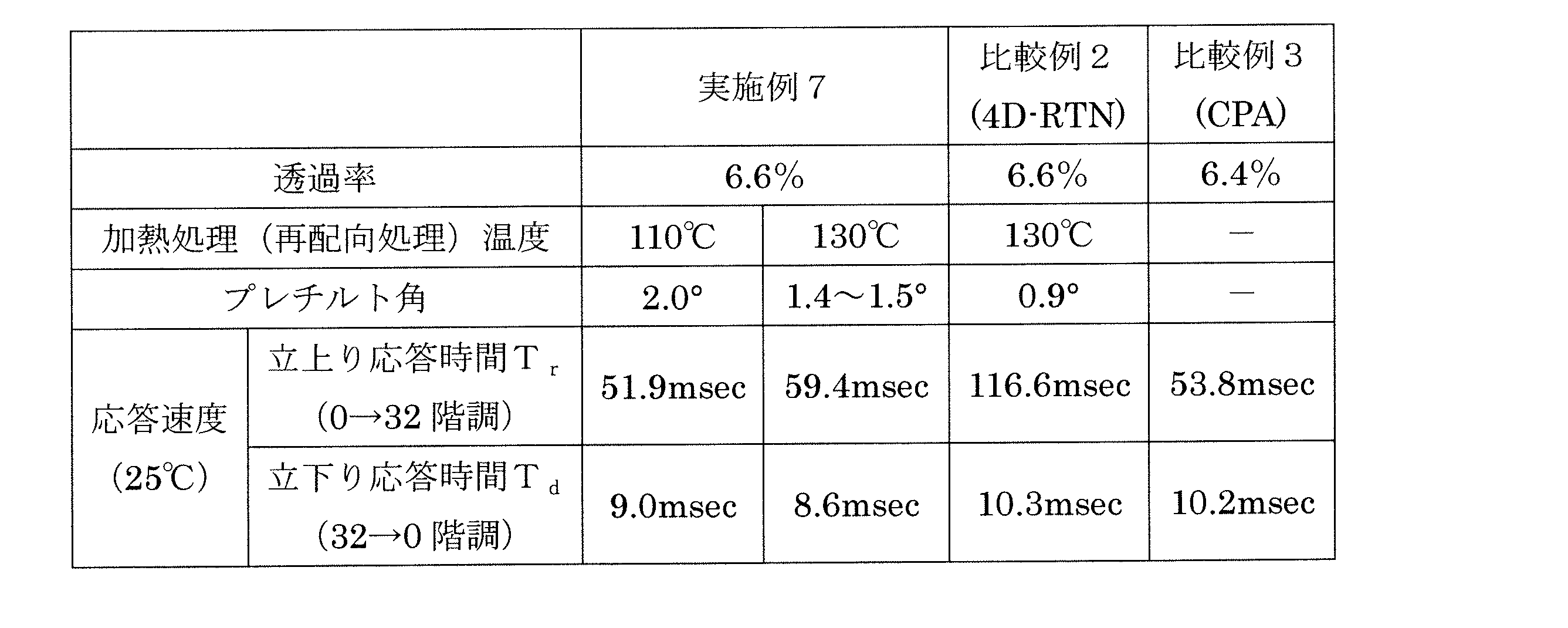
表3からわかるように、比較例2(4D-RTNモード)では、比較例3(CPAモード)に比べ、立上り応答時間Trが長く、2倍以上である。これは、既に説明したように不良チルト領域が画素内で占める割合が高くなることによって、平均的なプレチルト角が小さくなってしまっていることに起因していると考えられる。
これに対し、実施例7では、比較例3とほぼ同等の立上り応答時間が実現されている。これは、既に説明したように平均的なプレチルト角の低下が抑制されることが理由であると考えられる。
また、実施例7では、比較例3よりも高い透過率が実現されている。CPAモードでは、対向基板側に、軸対称配向の中心を固定して配向を安定化させるための配向規制手段(誘電体から形成される突起や対向電極に形成される開口部)が設けられることが多く、この配向規制手段が透過率の低下の原因となる。これに対し、本実施形態の液晶表示装置100は、そのような配向規制手段を必要としないので、高い透過率を実現することができる。
図20(a)および(b)に、実施例7および比較例2における階調と輝度(規格化輝度)との関係を、正面方向からの観察時、左右斜め60°方向からの観察時および上下斜め60°方向からの観察時について示す。図20(a)および(b)からわかるように、実施例7では、比較例2と同様に、γシフトの方位角依存性が小さく、十分に高い視野角特性が得られた。なお、ここでは図示しないが、比較例3でも、比較例2と同様の高い視野角特性が得られた。
また、上記表3において、実施例7として試作した2つの液晶表示装置100の比較からわかるように、再配向処理工程における加熱処理の温度が低い方が、平均的なプレチルト角をより大きくすることができる。具体的には、加熱処理を110℃以下で行うことが好ましい。ただし、液晶材料のネマチック相-等方相転移温度をTNIとしたとき、TNI+10℃未満の温度では、再配向処理の効果が十分に得られないことがあるので、加熱処理は、TNI+10℃以上であることが好ましい。
なお、加熱処理の温度が低い方が平均的なプレチルト角を大きくすることができる理由は、以下のように考えられる。
光配向膜によってプレチルト角が付与される(プレチルト方向が規定される)のは、光配向膜(典型的にはポリイミド系材料から形成される)に紫外線が照射された際に、光官能基の光反応によって側鎖が紫外線の入射側に向くからと考えられている。しかし、この反応は熱に対して可逆であるので、再配向処理工程における加熱処理を高温で長時間行うと元の(光配向処理を行う前の)プレチルト角(0°:基板面を基準にした場合には90°)に戻っていく。そのため、より低い温度で加熱処理を行うことが好ましいと考えられる。
ここで、図21(a)および(b)を参照しながら、比較例3として言及したCPAモードの基本構造を説明する。図21(a)および(b)は、CPAモードの液晶表示装置900の1つの画素を模式的に示す断面図および平面図である。
液晶表示装置900は、互いに対向するように配置されたアクティブマトリクス基板910および対向基板920と、これらの間に設けられた垂直配向型の液晶層930とを備える。
アクティブマトリクス基板910は、各画素に設けられた画素電極911と、画素電極911および液晶層930の間に設けられた垂直配向膜912とを有する。画素電極911および垂直配向膜912は、透明基板910aによって支持されている。
対向基板920は、画素電極911に対向する対向電極921と、対向電極921および液晶層930の間に設けられた垂直配向膜922とを有する。対向電極921および垂直配向膜922は、透明基板920aによって支持されている。対向電極921は、画素電極911の略中央に対向する領域に形成された開口部921aを有する。
液晶層930に電圧が印加されると、画素電極911の外縁近傍に生成される斜め電界の配向規制力と、対向電極921の開口部921a近傍に生成される斜め電界の配向規制力とによって、図21(a)および(b)に示すように、液晶分子931が軸対称配向する。
対向電極921の開口部921aは、軸対称配向の中心を固定し、配向を安定化させるように作用する。このように作用する配向規制手段として、対向電極921の開口部921aに代えて、誘電体から形成された突起(リベットと呼ばれることもある)を用いることもできる。ただし、配向規制手段近傍の液晶分子931は、電圧印加時に倒れにくい傾向があるので、そのことに起因して輝度が低下する。図21(c)に、液晶表示装置900(偏光板として円偏光板を備える)の液晶層930に白電圧を印加したときの透過率のシミュレーション結果を示す。図21(c)からわかるように、対向電極921の開口部921aに対応する領域は暗くなっており、輝度が低下している。
このような輝度の低下を抑制するために、配向規制手段自体のサイズ(対向電極921に形成された開口部921aの場合、一般的には直径10μm程度である)を小さくすることが考えられる。しかしながら、配向規制手段のサイズを小さくすると、配向規制力の不足によって配向状態を十分に安定化させることができなくなる可能性がある。また、微細な配向規制手段を形成するために高解像度のステッパ装置などの新たな設備を導入する必要もある。
そのため、配向規制手段のサイズはある程度以下には小さくできないので、高精細化に伴って画素ピッチが小さくなると、中心固定のための配向規制手段の画素全体に占める割合が増加することになる。CPAモードは、現在、中小型の液晶表示装置に採用されていることが多いが、上述した理由から、CPAモードの液晶表示装置では、高精細化に伴って画素ピッチが小さくなると、輝度が低下してしまう。
これに対し、本実施形態の液晶表示装置100では、特に偏光板として円偏光板を用いた場合、図8(c)などからもわかるように、輝度のロスが少なく、高い透過率を実現することができる。
既に説明したように、本実施形態における液晶表示装置100において応答速度が向上するのは、不良チルト領域NGRの面積が、4D-RTNモードの液晶表示装置に比べて小さくなるからであると考えられる。以下、本願発明者が、光の回折現象によって不良チルト領域NGRが実際に形成されるのかどうか、また、形成されるのであればどの程度の幅の不良プレチルト領域NGRが形成されるのかを検証した結果を説明する。
まず、図22(a)に示すように、光配向膜812が形成された基板810を用意し、この基板810の光配向膜812に、矢印で示す方向から紫外線を照射した。
次に、図22(b)に示すように、遮光部815がストライプ状に配列されたフォトマスクによって光配向膜812の一部の領域が遮光された状態で、矢印で示す方向(図22(a)に示した方向とは反対方向)から紫外線を照射した。
上述したように2回露光を行うことにより、光配向膜812には、図22(c)に示すように、1回だけ紫外線が照射された領域(第1領域)812aと、2回紫外線が照射された領域(第2領域)812bとが形成された。第1領域812aは、1回目の露光工程における紫外線照射により、大きいプレチルト角(具体的には2.5°)を付与し得る領域となった。これに対し、第2領域812bは、互いに反対方向から紫外線照射が行われる2回の露光工程のうちの2回目の露光工程における紫外線照射の影響をより強く受け、小さいプレチルト角(具体的には-0.5°)を付与し得る領域となった。
このようにして光配向膜812に2種類の領域812aおよび812bが形成された基板810を2枚用意し、図23に示すように、それらを所定の角度だけずらして(ここでは2°)貼り合わせた。貼り合わせによって得られたパネルの断面(図示している破線に沿った断面)に着目すると、第1領域812a同士が対向する領域および第2領域812b同士が対向する領域で構成される断面(「強調領域」と呼ぶ)と、第1領域812aと第2領域812bとが対向する領域のみで構成される断面(「相殺領域」と呼ぶ)と、それらが混在する断面(「中間領域」と呼ぶ)とが存在している。
図24に、強調領域、中間領域および相殺領域のそれぞれについて、プレチルト角のY方向(図23中の左右方向)に沿った位置プロファイルを示す。ここで、光の回折の影響を確認するため、強調領域におけるプレチルト角に注目する。図24には、フォトマスクの遮光部・透光部の位置も示されている。なお、フォトマスクなしで全面露光を一回だけ行った場合のプレチルト角は2.55°である。
図24からわかるように、フォトマスクの遮光部と透光部との境界を中心とした幅20~40μm程度の領域では、プレチルト角が2.5°から-0.5°に変化している。このことからわかるように、光の回折現象によってプレチルト角が低下する領域が実際に存在している。そのため、本実施形態における液晶表示装置100のように、第1光配向膜12の第1プレチルト領域12aおよび第2プレチルト領域12bの境界BD1全体と、第2光配向膜22の第3プレチルト領域22aおよび第4プレチルト領域22bの境界BD2全体とを重ねて不良チルト領域NGRの面積を小さくすることにより、画素1全体での平均的なプレチルト角の低下を抑制することができる。
続いて、実施例7(画面解像度217ppi、画素ピッチ39μm×117μm)として試作した2つの液晶表示装置100について、画素1内のプレチルト角の分布を測定した結果を説明する。図25(a)および(b)は、それぞれ、再配向処理工程における加熱処理の温度が110℃の場合と130℃の場合(時間はいずれも40分である)について、画素1内での位置とプレチルト角との関係を示すグラフである。なお、図25(a)および(b)のグラフの縦軸は、基板面に対するチルト角である。プレチルト角の測定は、図26中に示す方向Yに沿って行った。図26は、1つの画素1に対応する光学顕微鏡像である。
図25(a)および(b)から、プレチルト領域間の境界を中心とした幅20μm程度の領域は十分なプレチルト角を付与できない領域(不良チルト領域)になってしまっているものの、それ以外の領域は十分に大きなプレチルト角を実現できていることがわかる。
また、図25(a)と図25(b)との比較から、再配向処理工程における加熱処理の温度が低い方が、より大きなプレチルト角を実現できることがわかる。
なお、本実施形態の説明では、図5(a)および(b)に示したように、第1光配向膜12および第2光配向膜22が各画素1内で上下に2分割され、第1プレチルト方向PD1、第2プレチルト方向PD2、第3プレチルト方向PD3および第4プレチルト方向PD4がいずれも表示面の左右方向に略平行な場合を例示したが、配向分割の態様は例示したものに限定されない。例えば各画素が横長の形状を有している場合(画素の表示面左右方向に沿った長さが、表示面上下方向に沿った長さよりも大きい場合)には、第1光配向膜12および第2光配向膜22を各画素1内で左右に2分割し、第1プレチルト方向PD1、第2プレチルト方向PD2、第3プレチルト方向PD3および第4プレチルト方向PD4を表示面の上下方向に略平行としてもよい。
また、本実施形態では、1つのカラー表示画素が3つの画素から構成され、1つの画素の縦横比(アスペクト比)が3:1の構成を例示したが、1つのカラー表示画素を構成する画素数や画素の縦横比はここで例示したものに限定されない。
本発明の実施形態によると、光配向膜によって液晶分子のプレチルト方向が規定されるVAモードの液晶表示装置であって、高精細化に適した液晶表示装置が提供される。
1 画素
10 アクティブマトリクス基板
11 画素電極
11e1 第1エッジ部
11e2 第2エッジ部
12 第1光配向膜
12a 第1プレチルト領域
12b 第2プレチルト領域
18、28 偏光板(直線偏光板)
20 対向基板
21 対向電極
22 第2光配向膜
22a 第3プレチルト領域
22b 第4プレチルト領域
30 液晶層
31 液晶分子
100 液晶表示装置
e1 第1エッジ部に直交し画素電極の内側に向かう方向
e2 第2エッジ部に直交し画素電極の内側に向かう方向
A、B、C、D 液晶ドメイン
BD1 第1プレチルト領域および第2プレチルト領域の境界
BD2 第3プレチルト領域および第4プレチルト領域の境界
NGR、NGR1、NGR2 不良チルト領域
PD1 第1プレチルト方向
PD2 第2プレチルト方向
PD3 第3プレチルト方向
PD4 第4プレチルト方向
P1、P2 直線偏光板の透過軸
10 アクティブマトリクス基板
11 画素電極
11e1 第1エッジ部
11e2 第2エッジ部
12 第1光配向膜
12a 第1プレチルト領域
12b 第2プレチルト領域
18、28 偏光板(直線偏光板)
20 対向基板
21 対向電極
22 第2光配向膜
22a 第3プレチルト領域
22b 第4プレチルト領域
30 液晶層
31 液晶分子
100 液晶表示装置
e1 第1エッジ部に直交し画素電極の内側に向かう方向
e2 第2エッジ部に直交し画素電極の内側に向かう方向
A、B、C、D 液晶ドメイン
BD1 第1プレチルト領域および第2プレチルト領域の境界
BD2 第3プレチルト領域および第4プレチルト領域の境界
NGR、NGR1、NGR2 不良チルト領域
PD1 第1プレチルト方向
PD2 第2プレチルト方向
PD3 第3プレチルト方向
PD4 第4プレチルト方向
P1、P2 直線偏光板の透過軸
Claims (11)
- 互いに対向するように配置された第1基板および第2基板と、
前記第1基板および前記第2基板の間に設けられた垂直配向型の液晶層とを備え、
マトリクス状に配列された複数の画素を有する液晶表示装置であって、
前記第1基板は、前記複数の画素のそれぞれに設けられた画素電極と、前記画素電極および前記液晶層の間に設けられた第1光配向膜とを有し、
前記第2基板は、前記画素電極に対向する対向電極と、前記対向電極および前記液晶層の間に設けられた第2光配向膜とを有し、
前記第1光配向膜は、前記複数の画素のそれぞれ内において、第1プレチルト方向を規定する第1プレチルト領域と、前記第1プレチルト方向に反平行な第2プレチルト方向を規定する第2プレチルト領域とを有し、
前記第2光配向膜は、前記複数の画素のそれぞれ内において、第3プレチルト方向を規定する第3プレチルト領域と、前記第3プレチルト方向に反平行な第4プレチルト方向を規定する第4プレチルト領域とを有し、
表示面法線方向から見たとき、前記第1光配向膜の前記第1プレチルト領域および前記第2プレチルト領域の境界全体と、前記第2光配向膜の前記第3プレチルト領域および前記第4プレチルト領域の境界全体とが重なっている液晶表示装置。 - 表示面法線方向から見たとき、前記第1光配向膜の前記第1プレチルト領域と前記第2光配向膜の前記第3プレチルト領域とが重なっており、前記第1光配向膜の前記第2プレチルト領域と前記第2光配向膜の前記第4プレチルト領域とが重なっており、
前記第3プレチルト方向は、前記第1プレチルト方向に反平行であり、前記第4プレチルト方向は、前記第2プレチルト方向に反平行である請求項1に記載の液晶表示装置。 - 前記画素電極の外縁は、第1エッジ部および第2エッジ部を含み、
前記第1エッジ部に直交し前記画素電極の内側に向かう方向は、前記第1プレチルト方向とは反対の方向であり、
前記第2エッジ部に直交し前記画素電極の内側に向かう方向は、前記第2プレチルト方向とは反対の方向である請求項1または2に記載の液晶表示装置。 - 前記画素電極と前記対向電極との間に電圧が印加されたとき、前記複数の画素のそれぞれ内において前記液晶層に4つの液晶ドメインが形成され、
前記4つの液晶ドメインのそれぞれに含まれる前記液晶分子の配向方向を代表する4つのディレクタの方位は互いに異なる請求項1から3のいずれかに記載の液晶表示装置。 - 前記液晶層を介して互いに対向し、それぞれの透過軸が互いに略直交するように配置された一対の直線偏光板をさらに備え、
前記一対の直線偏光板の前記透過軸は、前記第1プレチルト方向と略45°の角をなす請求項1から4のいずれかに記載の液晶表示装置。 - 前記液晶層を介して互いに対向する一対の円偏光板をさらに備える請求項1から4のいずれかに記載の液晶表示装置。
- 前記液晶層は、負の誘電異方性を有する液晶分子を含む請求項1から6のいずれかに記載の液晶表示装置。
- 表示面水平方向に沿った画素ピッチおよび表示面垂直方向に沿った画素ピッチのうちの短い方の画素ピッチが42μm以下である請求項1から7のいずれかに記載の液晶表示装置。
- 画面解像度が200ppi以上である請求項1から8のいずれかに記載の液晶表示装置。
- 互いに対向するように配置された第1基板および第2基板と、前記第1基板および前記第2基板の間に設けられた垂直配向型の液晶層とを備え、マトリクス状に配列された複数の画素を有し、
前記第1基板は、前記複数の画素のそれぞれに設けられた画素電極と、前記画素電極および前記液晶層の間に設けられた第1光配向膜とを有し、前記第2基板は、前記画素電極に対向する対向電極と、前記対向電極および前記液晶層の間に設けられた第2光配向膜とを有する液晶表示装置の製造方法であって、
前記第1光配向膜の、前記複数の画素のそれぞれに対応する領域内に、第1プレチルト方向を規定する第1プレチルト領域と、前記第1プレチルト方向に反平行な第2プレチルト方向を規定する第2プレチルト領域とを光配向処理によって形成する工程(A)と、
前記第2光配向膜の、前記複数の画素のそれぞれに対応する領域内に、第3プレチルト方向を規定する第3プレチルト領域と、前記第3プレチルト方向に反平行な第4プレチルト方向を規定する第4プレチルト領域とを光配向処理によって形成する工程(B)と、
前記工程(A)および前記工程(B)の後に、前記第1基板と前記第2基板とを貼り合わせる工程(C)と、を包含し、
前記工程(A)および前記工程(B)は、前記工程(C)において前記第1基板と前記第2基板とを貼り合わせたときに、表示面法線方向から見て、前記第1光配向膜の前記第1プレチルト領域および前記第2プレチルト領域の境界全体と、前記第2光配向膜の前記第3プレチルト領域および前記第4プレチルト領域の境界全体とが重なるように実行される液晶表示装置の製造方法。 - 前記工程(C)の後に、前記液晶層に加熱処理を含む再配向処理を施す工程(D)をさらに包含し、
前記加熱処理は、110℃以下で行われる請求項10に記載の液晶表示装置の製造方法。
Priority Applications (1)
| Application Number | Priority Date | Filing Date | Title |
|---|---|---|---|
| US14/899,841 US9933662B2 (en) | 2013-06-20 | 2014-02-27 | Liquid crystal display device and method for manufacturing same |
Applications Claiming Priority (2)
| Application Number | Priority Date | Filing Date | Title |
|---|---|---|---|
| JP2013-129989 | 2013-06-20 | ||
| JP2013129989 | 2013-06-20 |
Publications (1)
| Publication Number | Publication Date |
|---|---|
| WO2014203565A1 true WO2014203565A1 (ja) | 2014-12-24 |
Family
ID=52104311
Family Applications (1)
| Application Number | Title | Priority Date | Filing Date |
|---|---|---|---|
| PCT/JP2014/054961 Ceased WO2014203565A1 (ja) | 2013-06-20 | 2014-02-27 | 液晶表示装置およびその製造方法 |
Country Status (2)
| Country | Link |
|---|---|
| US (1) | US9933662B2 (ja) |
| WO (1) | WO2014203565A1 (ja) |
Families Citing this family (2)
| Publication number | Priority date | Publication date | Assignee | Title |
|---|---|---|---|---|
| CN110764315B (zh) * | 2019-10-28 | 2022-05-03 | Tcl华星光电技术有限公司 | 液晶配向力仿真方法、系统、设备及存储介质 |
| CN114879414A (zh) * | 2022-04-26 | 2022-08-09 | 成都中电熊猫显示科技有限公司 | 一种显示面板和显示装置 |
Citations (3)
| Publication number | Priority date | Publication date | Assignee | Title |
|---|---|---|---|---|
| JPH07281187A (ja) * | 1994-02-17 | 1995-10-27 | Stanley Electric Co Ltd | 液晶表示素子の製造方法 |
| JP2000131698A (ja) * | 1998-10-27 | 2000-05-12 | Stanley Electric Co Ltd | 液晶表示素子とその製造方法 |
| WO2011161921A1 (ja) * | 2010-06-23 | 2011-12-29 | シャープ株式会社 | 液晶表示装置 |
Family Cites Families (7)
| Publication number | Priority date | Publication date | Assignee | Title |
|---|---|---|---|---|
| US5712696A (en) | 1994-02-17 | 1998-01-27 | Stanley Electric, Co., Ltd. | Manufacture of LCD device by transferring the orientation state from a parent substrate to a child substrate |
| TW589504B (en) | 1997-06-12 | 2004-06-01 | Sharp Kk | Liquid crystal display device |
| JP3601786B2 (ja) | 2000-08-11 | 2004-12-15 | シャープ株式会社 | 液晶表示装置 |
| JP3601788B2 (ja) | 2000-10-31 | 2004-12-15 | シャープ株式会社 | 液晶表示装置 |
| JP4666398B2 (ja) | 2005-05-13 | 2011-04-06 | シャープ株式会社 | 液晶表示装置 |
| US7995177B2 (en) | 2005-06-09 | 2011-08-09 | Sharp Kabushiki Kaisha | Liquid crystal display device |
| CN105705988A (zh) * | 2013-10-21 | 2016-06-22 | 夏普株式会社 | 液晶显示装置 |
-
2014
- 2014-02-27 WO PCT/JP2014/054961 patent/WO2014203565A1/ja not_active Ceased
- 2014-02-27 US US14/899,841 patent/US9933662B2/en active Active
Patent Citations (3)
| Publication number | Priority date | Publication date | Assignee | Title |
|---|---|---|---|---|
| JPH07281187A (ja) * | 1994-02-17 | 1995-10-27 | Stanley Electric Co Ltd | 液晶表示素子の製造方法 |
| JP2000131698A (ja) * | 1998-10-27 | 2000-05-12 | Stanley Electric Co Ltd | 液晶表示素子とその製造方法 |
| WO2011161921A1 (ja) * | 2010-06-23 | 2011-12-29 | シャープ株式会社 | 液晶表示装置 |
Also Published As
| Publication number | Publication date |
|---|---|
| US9933662B2 (en) | 2018-04-03 |
| US20160139466A1 (en) | 2016-05-19 |
Similar Documents
| Publication | Publication Date | Title |
|---|---|---|
| CN102116965B (zh) | 液晶显示装置 | |
| JP5881057B2 (ja) | 横電界方式の液晶表示装置及びその製造方法 | |
| US8525965B2 (en) | Liquid crystal display panel with unit pixels having slits in pixel electrode and photo alignment layers | |
| JP6347937B2 (ja) | 液晶表示装置 | |
| JP5209754B2 (ja) | 液晶表示装置 | |
| US20120229739A1 (en) | Liquid crystal display device and manufacturing method therefor | |
| KR20150012093A (ko) | 액정 표시 장치 및 그 제조 방법 | |
| WO2013054828A1 (ja) | 液晶表示装置 | |
| JPWO2009122864A1 (ja) | カラーフィルタ基板及び液晶表示装置 | |
| WO2010119659A1 (ja) | 液晶表示装置 | |
| US10718978B2 (en) | Apparatus for improving optical alignment of panels manufactured on a same mother substrate | |
| WO2015060001A1 (ja) | 液晶表示装置 | |
| WO2011013649A1 (ja) | 液晶表示装置およびその製造方法 | |
| WO2012147722A1 (ja) | 液晶表示装置 | |
| JPWO2014034471A1 (ja) | 液晶表示装置 | |
| CN110446971B (zh) | 液晶显示装置 | |
| JP2009109767A (ja) | 液晶表示装置 | |
| JP2011133910A (ja) | 液晶表示装置及びその製造方法 | |
| JP2009186822A (ja) | 液晶表示パネル及び液晶表示パネルの製造方法 | |
| WO2014203565A1 (ja) | 液晶表示装置およびその製造方法 | |
| WO2013022075A1 (ja) | 液晶表示装置 | |
| JP6086403B2 (ja) | 横電界方式の液晶表示装置及びその製造方法 | |
| WO2014196495A1 (ja) | 液晶表示装置の製造方法 | |
| US20060285056A1 (en) | Wide viewing angle liquid crystal display and the method for achieving wide viewing angle effect | |
| WO2023206535A1 (zh) | 一种显示面板及其制造方法、显示装置 |
Legal Events
| Date | Code | Title | Description |
|---|---|---|---|
| 121 | Ep: the epo has been informed by wipo that ep was designated in this application |
Ref document number: 14814007 Country of ref document: EP Kind code of ref document: A1 |
|
| WWE | Wipo information: entry into national phase |
Ref document number: 14899841 Country of ref document: US |
|
| NENP | Non-entry into the national phase |
Ref country code: DE |
|
| 122 | Ep: pct application non-entry in european phase |
Ref document number: 14814007 Country of ref document: EP Kind code of ref document: A1 |
|
| NENP | Non-entry into the national phase |
Ref country code: JP |