WO2014203458A1 - 発光素子 - Google Patents
発光素子 Download PDFInfo
- Publication number
- WO2014203458A1 WO2014203458A1 PCT/JP2014/002738 JP2014002738W WO2014203458A1 WO 2014203458 A1 WO2014203458 A1 WO 2014203458A1 JP 2014002738 W JP2014002738 W JP 2014002738W WO 2014203458 A1 WO2014203458 A1 WO 2014203458A1
- Authority
- WO
- WIPO (PCT)
- Prior art keywords
- semiconductor layer
- layer
- electrode portion
- pad electrode
- light emitting
- Prior art date
- Legal status (The legal status is an assumption and is not a legal conclusion. Google has not performed a legal analysis and makes no representation as to the accuracy of the status listed.)
- Ceased
Links
Images






Classifications
-
- H—ELECTRICITY
- H10—SEMICONDUCTOR DEVICES; ELECTRIC SOLID-STATE DEVICES NOT OTHERWISE PROVIDED FOR
- H10H—INORGANIC LIGHT-EMITTING SEMICONDUCTOR DEVICES HAVING POTENTIAL BARRIERS
- H10H20/00—Individual inorganic light-emitting semiconductor devices having potential barriers, e.g. light-emitting diodes [LED]
- H10H20/80—Constructional details
- H10H20/83—Electrodes
- H10H20/831—Electrodes characterised by their shape
-
- H—ELECTRICITY
- H10—SEMICONDUCTOR DEVICES; ELECTRIC SOLID-STATE DEVICES NOT OTHERWISE PROVIDED FOR
- H10H—INORGANIC LIGHT-EMITTING SEMICONDUCTOR DEVICES HAVING POTENTIAL BARRIERS
- H10H20/00—Individual inorganic light-emitting semiconductor devices having potential barriers, e.g. light-emitting diodes [LED]
- H10H20/80—Constructional details
- H10H20/83—Electrodes
- H10H20/832—Electrodes characterised by their material
-
- H—ELECTRICITY
- H10—SEMICONDUCTOR DEVICES; ELECTRIC SOLID-STATE DEVICES NOT OTHERWISE PROVIDED FOR
- H10H—INORGANIC LIGHT-EMITTING SEMICONDUCTOR DEVICES HAVING POTENTIAL BARRIERS
- H10H20/00—Individual inorganic light-emitting semiconductor devices having potential barriers, e.g. light-emitting diodes [LED]
- H10H20/80—Constructional details
- H10H20/81—Bodies
- H10H20/822—Materials of the light-emitting regions
- H10H20/824—Materials of the light-emitting regions comprising only Group III-V materials, e.g. GaP
Definitions
- the present invention relates to a compound semiconductor light emitting device, and more particularly to a compound semiconductor light emitting device having a pad electrode portion.
- LEDs light emitting diodes
- a small module is required, which requires a smaller volume for the chip.
- the chip thickness determines the thickness of the module, realizing a thin chip is the key to reducing the volume.
- a thin light emitting element cannot provide an epitaxial film thickness sufficient for current diffusion. In a light-emitting element that does not perform sufficient current diffusion, the current concentrates on a part of the light-emitting element, so that light emission is particularly easily performed directly under the electrode, and the EL (Electro-Luminescence) emission distribution is not uniform. Light output cannot be earned.
- Patent Document 1 it has been proposed to provide a block layer made of an insulator such as SiO 2 immediately below the electrode.
- Patent Document 2 describes that a transparent conductive layer is provided, a reduction electrode containing a substance that reduces the transparent electrode layer is provided in the pad electrode, and a block layer is provided below the reduction electrode layer.
- Patent Document 1 proposes a Patent Document 2 .
- Patent Document 2 in which the transparent conductive layer and the pad metal part form an alloy layer has a more preferable structure than Patent Document 1, but the formation of the transparent conductive layer, the formation of the reduction electrode layer, and the like.
- the photolithography process, electrode pattern formation, and Patent Document 2 require more processes than Patent Document 1.
- providing the block layer as an epitaxial layer is not a preferable method for manufacturing an inexpensive chip because it causes a much larger cost increase than providing an SiO 2 film or a transparent conductive film.
- Patent Document 1 and Patent Document 2 are effective in preventing current from flowing directly under the pad electrode, many additional steps are required, and the cost for forming the electrode increases. Then, it was difficult to reduce the chip cost while maintaining the light emission output.
- the present invention has been made in view of the above problems, and an object of the present invention is to provide a light emitting element having a chip structure that is inexpensive and can suppress the occurrence of electrode peeling while maintaining the light output from the chip. .
- the present invention provides a light emitting part in which at least a first semiconductor layer having a first conductivity type, an active layer, and a second semiconductor layer having a second conductivity type are formed in this order; A first electrode part having a pad electrode part in contact with the two semiconductor layers and a thin wire electrode part in contact with the second semiconductor layer and connected to the pad electrode part; and a second electrode part provided on the first semiconductor layer side
- the pad electrode portion includes one or more kinds of metals of Al, Ag, Au, Pt, Cu, Ti, and Ni.
- the pad electrode portion does not include a metal that becomes a p-type dopant or a metal that becomes an n-type dopant with respect to the second semiconductor layer, or p with respect to the second semiconductor layer.
- the thin wire electrode part is composed of one or more layers including one or more kinds of metals of Al, Ag, Au, Pt, Cu, Ti, and Ni, and the thin wire electrode part is formed in the second semiconductor layer.
- the pad electrode portion is any one of Al, Ag, Au, Pt, Cu, Ti, and Ni.
- the pad electrode portion does not contain a metal that becomes a p-type dopant or a metal that becomes an n-type dopant with respect to the second semiconductor layer, or the second
- the semiconductor layer includes one or more kinds of metals serving as n-type dopants
- the thin wire electrode portion includes one or more kinds of metals including any one or more kinds of metals of Al, Ag, Au, Pt, Cu, Ti, and Ni. It has a layer structure, and the thin wire electrode part is To provide a light emitting device characterized by comprising 1 or more metals to be a p-type dopant with respect to the second semiconductor layer.
- the pad electrode portion, the fine wire electrode portion, and the second semiconductor layer are configured as described above, so that ohmic contact is not caused between the pad electrode portion and the second semiconductor layer, and Schottky is provided. Because the contact is made, the region immediately below the pad electrode portion has high resistance, while the thin wire electrode portion and the second semiconductor layer are in ohmic contact and the region immediately below the thin wire electrode portion has low resistance. Since current does not flow and current flows only in the thin wire electrode portion, the current concentrates in the thin wire electrode portion, and the same effect as when a block layer is provided directly below the pad electrode can be obtained. A light emitting element can be realized.
- a window layer having a thickness of 10 ⁇ m or more is formed on the side of the first semiconductor layer opposite to the active layer.
- composition adjustment layer between the first semiconductor layer and the window layer.
- the window layer can be epitaxially grown.
- a supporting substrate having the second electrode on the lower surface, a bonding metal layer provided on the supporting substrate and functioning as a reflective layer, and a dielectric provided between the bonding metal layer and the first semiconductor layer
- the semiconductor device may further include a body layer and an interface electrode that penetrates a part of the dielectric layer and contacts the bonding metal layer and the first semiconductor layer.
- the second semiconductor layer is made of an AlGaInP-based compound semiconductor, an AlGaInN-based compound semiconductor, or an AlGaAs-based compound semiconductor
- the metal serving as a p-type dopant for the second semiconductor layer is Be, Zn, Mg , C, and the metal serving as an n-type dopant for the second semiconductor layer may be any of S, Se, Si, and Ge.
- the second semiconductor layer is made of an AlGaInP-based compound semiconductor, an AlGaInN-based compound semiconductor, or an AlGaAs-based compound semiconductor, the above dopant metal can be preferably used.
- the thickness of the pad electrode part is 200 nm or more thicker than the fine wire electrode part, and the width of the electrode at the boundary between the pad electrode part and the fine wire electrode part is 5 ⁇ m or more.
- the thickness which can absorb the impact at the time of wire bonding is securable.
- the electrode width at the boundary between the pad electrode portion and the fine wire electrode portion as described above, the pad electrode portion and the fine wire electrode portion can be electrically connected with a low resistance.
- the active layer is made of (Al x Ga 1-x ) y In 1-y P (0 ⁇ x ⁇ 1, 0.35 ⁇ y ⁇ 0.65), and the first semiconductor layer and the second semiconductor layer Can be made of (Al x Ga 1-x ) y In 1-y P (0 ⁇ x ⁇ 1, 0.35 ⁇ y ⁇ 0.65).
- the active layer is made of (Al x Ga 1-x ) y In 1-y N (0 ⁇ x ⁇ 1, 0 ⁇ y ⁇ 1), and the first semiconductor layer and the second semiconductor layer are (Al x Ga 1-x ) y In 1-y N (0 ⁇ x ⁇ 1, 0 ⁇ y ⁇ 1).
- the active layer is made of (Al x Ga 1-x ) As (0 ⁇ x ⁇ 1), and the first semiconductor layer and the second semiconductor layer are (Al x Ga 1-x ) As (0 ⁇ x ⁇ 1 ). 1) or (Al x Ga 1-x ) y In 1-y P (0 ⁇ x ⁇ 1, 0.35 ⁇ y ⁇ 0.65).
- the above materials can be suitably used as the active layer, the first semiconductor layer, and the second semiconductor layer of the light emitting unit.
- the dopant metal contained in the pad electrode portion and the fine wire electrode portion is changed according to the conductivity type of the second semiconductor layer, thereby suppressing the current flowing directly under the pad electrode portion.
- an alloy layer can be formed at the interface between the pad electrode part and the second semiconductor layer. A light-emitting element having a chip structure that can be suppressed can be realized.
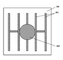
- FIG. 6 is a top view of a light emitting element of Comparative Example 1.
- FIG. 6 is a top view of a light emitting device of Comparative Example 2.
- FIG. FIG. 10 is a top view of a light emitting element of Comparative Example 3.
- 6 is a top view of a light emitting device of Comparative Example 4.
- FIG. It is a graph which shows the relative light emission output with respect to Example 1 of the comparative example 1 thru
- FIG. It is a graph which shows the ratio of the light emission output of the light emitting element of Example 2 with respect to the light emitting element of the comparative example 4, VF value, and luminous efficiency.
- the inventors have made extensive studies on a light emitting element that can reduce the chip cost while maintaining the light emission output.
- the dopant metal contained in the pad electrode portion and the fine wire electrode portion according to the conductivity type of the second semiconductor layer, the current flowing directly under the pad electrode portion is suppressed, while the current is directly under the fine wire electrode portion.
- an alloy layer can be formed at the interface between the pad electrode portion and the second semiconductor layer, the chip cost can be reduced while maintaining the light emission output, and the occurrence of electrode peeling can be suppressed.
- the headline and the present invention were made.
- FIG. 1 is a cross-sectional view of an epitaxial wafer used for manufacturing the light emitting device of the first embodiment of the present invention.
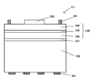
- FIG. 2 is a schematic cross-sectional view of the light emitting device of the first embodiment of the present invention.
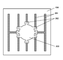
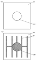
- FIG. 3 is a top view (a plan view seen from the second semiconductor layer side) of the light emitting device according to the first embodiment of the present invention.
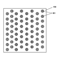
- FIG. 4 is a bottom view (a plan view seen from the window layer side) of the light emitting device according to the first embodiment of the present invention. As shown in FIG.
- an epitaxial wafer 100 is formed with a buffer layer 102 and an etching stop layer 103 on a starting substrate 101, and then a second conductivity type second semiconductor layer 104, an active layer 105, a first conductivity type.
- the light emitting portion 120 is formed by stacking the first semiconductor layers 106.
- the material of the light emitting part is (Al x Ga 1-x ) y In 1-y P (0 ⁇ x ⁇ 1, 0, 35 ⁇ y ⁇ 0.65), Al z Ga 1-z As (0 ⁇ z ⁇ 1) or (Al x Ga 1-x ) y In 1-y N (0 ⁇ x ⁇ 1, 0 ⁇ y ⁇ 1) can be selected.
- the buffer layer 102 is a layer including an effect of adjusting the lattice irregularity.
- the active layer 105 is adjusted to a composition having a band gap smaller than that of the first semiconductor layer 106 and the second semiconductor layer 104 in order to produce a carrier confinement effect.
- a window layer 108 is formed on the light emitting unit 120 by epitaxial growth.
- the window layer 108 can be selected from any material that does not diffuse impurities into the substrate during growth, but is transparent to the light emitted from the active layer 105.
- Certain GaPAs, GaP, AlGaAs, AlAs, GaPN, etc. can be selected.
- the thicker the window layer 108 the higher the light extraction effect.
- an increase in light extraction effect can be expected even with a thickness of about 1 ⁇ m, it is preferable to provide a window layer with a thickness of 10 ⁇ m or more for a later process.
- the lattice constants are significantly different between the window layer 108 and the second semiconductor layer 106, it is more effective to suppress the surface roughness by providing the composition adjustment layer 107, but there is no composition adjustment layer 107. May be.
- the second semiconductor layer 104 is effectively provided with a region having two or more kinds of doping concentrations in order to enhance the current dispersion effect.
- a pair of layers having different doping concentrations such that the doping concentration of one layer is more than twice the doping concentration of the other layer from the region on the starting substrate 101 side of the second semiconductor layer 104 to the direction in contact with the active layer 105 It is preferable to arrange one or more sets. That is, current is dispersed in the lateral direction at the interface between the low-concentration doping layer and the high-concentration doping layer, and the current flows through the high-concentration doping layer with low resistance, thereby realizing effective current dispersion even in a thin film. be able to. When a plurality of pairs of the low-concentration doping layer and the high-concentration doping layer are combined, the effect of current dispersion can be further enhanced.
- the effect of current dispersion is remarkable in the region where the doping concentration of the low-concentration doping layer is 3 ⁇ 10 17 / cm 3 or less and the doping concentration of the high-concentration doping layer is 6 ⁇ 10 17 / cm 3. Three or more areas.
- the effect of current dispersion is an effect due to a difference in doping concentration, and the low-concentration doping layer only needs to have a thickness of 50 nm or more when the epitaxial layer is formed. Even if the low concentration doping layer is higher than 3 ⁇ 10 17 / cm 3 and the high concentration doping layer is less than 6 ⁇ 10 17 / cm 3 , two or more pairs of the low concentration doping layer and the high concentration doping layer can be provided. In this case, since the film thickness is increased, the cost can be increased, but the same effect can be obtained.
- the window layer 108 is of the first conductivity type (that is, the same conductivity type as the first semiconductor layer 106), and preferably has a doping concentration of 1 ⁇ 10 17 / cm 3 or more.
- the doping concentration of the first semiconductor layer 106 is uniform and the doping concentration of the region of the window layer 108 is less than 1 ⁇ 10 17 / cm 3 , current dispersion is inhibited and light emission from the active layer is uniform. It may not be possible.
- the doping concentration in the region of the window layer 108 is less than 1 ⁇ 10 17 / cm 3
- the first semiconductor layer is formed in the same manner as the second semiconductor layer 104 in order to make current distribution uniform.
- 106 preferably has two types of doping regions of low concentration and high concentration.
- a dot electrode 401 is formed so as to be in contact with the window layer 108 as shown in FIG.
- the starting substrate 101 and the buffer layer 102 are removed.
- the starting substrate 101 is GaAs
- it is removed with a mixed solution of ammonia and hydrogen peroxide.
- the etching stopper layer 103 is an AlInP layer
- the etching stop layer 103 is removed, and the second semiconductor layer 104 is exposed.
- the etching stopper layer 103 can be selectively removed by using, for example, an SPM (sulfuric acid / hydrogen peroxide) solution.
- the exposed second semiconductor layer 104 has a structure of one or more layers made of a metal including one or more of Al, Ag, Au, Pt, Cu, Ti, and Ni.
- a thin wire electrode portion 301 is formed.
- the second conductivity type that is, the conductivity type of the second semiconductor layer 104
- the thin wire electrode portion 301 has one or more kinds of metals of Be, Zn, Mg, and C (that is, the second semiconductor layer 104).
- the thin wire electrode portion 301 includes one or more kinds of metals of S, Se, Si, and Ge (that is, a metal that becomes an n-type dopant with respect to the second semiconductor layer 104). .
- the thin wire electrode portion 301 is an electrode portion having a function of dispersing current in the second semiconductor layer 104. Therefore, when the cross-sectional area is reduced, the resistance is increased and the current dispersion function cannot be performed.
- Al, Ag, Au, Pt, Cu, Ti, Ni, and the like are metals having a sufficiently low resistance to be used for current dispersion of the light emitting element, but have a limited cross-sectional area. Therefore, it is preferable to provide a cross-sectional area of 0.1 ⁇ m 2 or more.
- the second conductivity type is n-type
- a Ti layer of 100 nm, an AuGe alloy layer of 50 nm, and an Au layer of 100 nm are stacked on the second semiconductor layer 104 by vapor deposition.
- the Au layer may be Ag, Al, Pt, or Cu, and the Ti layer may be omitted or replaced with Ni.
- the stacking order is not limited to the order presented in the present embodiment.
- the film thickness is not limited to this example, and can be freely selected within the range of a cross-sectional area of 0.1 ⁇ m 2 or more. Therefore, if the width of the thin wire electrode 301 is increased, it can be made thinner than this example. Needless to say, if it becomes narrower, it can be made thicker than this example.
- an AuGe alloy is used as the dopant source Ge. This is because the alloy is easier to handle in the vapor deposition method.
- a method other than the vapor deposition method such as a sputtering method, a MOVPE (metal organic chemical vapor deposition) method, or an MBE (molecular beam epitaxy) method
- only Ge may be used.
- S, Se, and Si the same applies to S, Se, and Si.
- the AuGe alloy layer in the previous example may be replaced with an alloy layer such as AuZn. Even if the second conductivity type is p-type, the stacking order is not limited to the previous example, and various orders can be selected.
- the pad electrode portion 303 is formed so as to have a region 302 that overlaps with the thin wire electrode portion 301.
- the pad electrode portion 303 is formed of a metal including at least one of Al, Ag, Au, Pt, Cu, Ti, and Ni.
- the pad electrode portion 303 has one or more kinds of metals of S, Se, Si, and Ge (that is, a metal that becomes an n-type dopant with respect to the second semiconductor layer 104). Or does not contain any metal of Be, Zn, Mg, C, S, Se, Si, or Ge (that is, a metal that becomes a p-type dopant for the second semiconductor layer 104 is also an n-type dopant).
- the pad electrode portion 303 is made of at least one of Be, Zn, Mg, and C (that is, a metal that becomes a p-type dopant with respect to the second semiconductor layer 104). Or any metal of Be, Zn, Mg, C, S, Se, Si, and Ge is not included (that is, the metal serving as the p-type dopant for the second semiconductor layer 104 is also n-type). (The metal which does not contain a dopant is not included).
- a Ti layer of 100 nm and an Au layer of 900 nm are stacked on the second semiconductor layer 104 as the pad electrode portion 303.
- the Au layer may be Ag, Al, Pt, or Cu, and the Ti layer may be omitted or replaced with Ni.
- the Ti layer is a single layer above the Ti layer, but various combinations of structures such as a structure in which Al and Au are laminated or a structure in which Ag and Au are laminated can be selected.
- the thickness of the pad electrode portion 303 is 1000 nm. However, since it is sufficient to provide a thickness that can absorb an impact at the time of wire bonding, the thickness is not limited to this example, and may be thin. .
- the thickness of the pad electrode portion 303 is 200 nm or more thicker than that of the thin wire electrode portion 301.
- the thickness which can absorb the impact at the time of wire bonding is securable by making the thickness of the pad electrode part 303 200 nm or more thicker than the thin wire
- the width of the electrode (overlapping region 302) at the boundary between the pad electrode portion 303 and the thin wire electrode portion is preferably 5 ⁇ m or more.
- Heat treatment is performed in a state where the fine wire electrode portion 301 and the pad electrode portion 303 are formed.
- an alloy layer is formed on the semiconductor layer in contact with the metal. Since mutual diffusion occurs from the metal layer to the semiconductor layer and from the semiconductor layer to the metal layer when forming the alloy layer, a mechanically strong layer is formed. Peeling phenomenon of the electrode part at the time of wire bonding occurs at the interface between the layers, but a layer whose composition changes continuously through the alloy layer is formed between the metal of the electrode part and the semiconductor layer by heat treatment. Since the interface does not exist, it is possible to prevent the electrode portion from peeling from the semiconductor layer during wire bonding.
- the resistance of the semiconductor even if the dopant metal diffuses into the semiconductor layer by heat treatment Rather, it acts as an effect of increasing the resistance of the semiconductor layer by compensating the p-type dopant. As a result, the resistance with the semiconductor layer in contact with the pad electrode portion 303 becomes very large.
- the pad electrode portion 303 includes one or more dopant metals of Be, Zn, Mg, and C
- the resistance of the semiconductor even if the dopant metal diffuses into the semiconductor layer by heat treatment Rather, it acts as an effect of increasing the resistance of the semiconductor layer by compensating the n-type dopant.
- the resistance with the semiconductor layer in contact with the pad electrode portion 303 becomes very large.
- the pad electrode portion 303 When the pad electrode portion 303 is formed with a structure that does not include any of the doped metals Be, Zn, Mg, C, S, Se, Si, and Ge, the dopant metal does not diffuse into the semiconductor layer due to the heat treatment, so the semiconductor layer side The resistance does not decrease. Therefore, the resistance with the semiconductor layer in contact with the pad electrode portion 303 is increased.
- the light emitting element 121 having a structure in which current selectively flows through the thin wire electrode portion 301 and current does not flow through the pad electrode portion 303 or is extremely difficult to flow.
- FIG. 5 is a cross-sectional view of an epitaxial wafer used for manufacturing the light emitting device of the second embodiment of the present invention.
- FIG. 6 is a process cross-sectional view illustrating a manufacturing process of the light emitting device according to the second embodiment of the present invention.
- FIG. 7 is a schematic cross-sectional view of a light emitting device according to the second embodiment of the present invention.
- FIG. 8 is a top view (a plan view seen from the second semiconductor layer side) of the light emitting device according to the second embodiment of the present invention. As shown in FIG.
- the epitaxial wafer 500 is formed with a buffer layer 502 and an etching stop layer 503 on a starting substrate 501, and then a second conductivity type second semiconductor layer 504, an active layer 505, a first conductivity type.
- the light emitting portion 520 is formed by stacking the first semiconductor layers 506.
- the material of the light emitting part is (Al x Ga 1-x ) y In 1-y P (0 ⁇ x ⁇ 1, 0, 35 ⁇ y ⁇ 0.65), Al z Ga 1-z As (0 ⁇ z ⁇ 1) or (Al x Ga 1-x ) y In 1-y N (0 ⁇ x ⁇ 1, 0 ⁇ y ⁇ 1) can be selected.
- the buffer layer 502 is a layer including an effect of adjusting the lattice mismatch.
- the active layer 505 is adjusted to a composition having a smaller band gap than the first semiconductor layer 506 and the second semiconductor layer 504 in order to produce a carrier confinement effect.
- the contact layer 507 is not necessarily provided.
- the contact layer 507 is preferably provided with a doping concentration of 3 ⁇ 10 18 / cm 3 or more in order to form an ohmic with the electrode, but in particular, it has a doping concentration of 6 ⁇ 10 18 / cm 3 or more. Is preferred.
- the second semiconductor layer 504 is effectively provided with a region having two or more kinds of doping concentrations in order to enhance the current dispersion effect.
- a pair of layers having different doping concentrations such that the doping concentration of one layer is more than twice the doping concentration of the other layer from the region on the starting substrate 501 side of the second semiconductor 504 to the direction in contact with the active layer 505 is 1 It is preferable to arrange more than one group.
- the current is dispersed in the lateral direction at the interface between the low-concentration doping layer and the high-concentration doping layer, and the current flows with low resistance in the high-concentration doping layer, so that effective current dispersion is realized even in a thin film.
- the effect of current dispersion can be further enhanced.
- the effect of current dispersion is remarkable in the region where the doping concentration of the low-concentration doping layer is 3 ⁇ 10 17 / cm 3 or less and the doping concentration of the high-concentration doping layer is 6 ⁇ 10 17 / cm 3. Three or more areas.
- the effect of current dispersion is an effect due to a difference in doping concentration, and the low-concentration doping layer only needs to have a thickness of 50 nm or more when the epitaxial layer is formed.
- the low concentration doping layer is higher than 3 ⁇ 10 17 / cm 3 and the high concentration doping layer is less than 6 ⁇ 10 17 / cm 3 , two or more pairs of the low concentration doping layer and the high concentration doping layer can be provided. In this case, since the film thickness is increased, the cost can be increased, but the same effect can be obtained.
- a dielectric film 601 is provided on the contact layer 507 after the contact layer 507 is formed.
- the dielectric film 601 can be selected from silicon oxide, silicon nitride, gallium oxide, sapphire, and the like.
- the etching can be easily performed by selecting a silicon oxide film or a silicon nitride film.
- pattern formation is performed by dry etching, all the above materials can be selected. In the present embodiment, the case of a silicon oxide film is illustrated, but the same effect can be obtained even if the other material is selected.
- the first bonding metal layer 604 is formed of a metal including at least one of Al, Ag, Au, Pt, Cu, Ti, and Ni.
- the first bonding metal layer 604 may have a laminated structure in which a plurality of the above metals are combined. It is good also as a layer of.
- a second bonding metal layer 621 is formed on the support substrate 620 to form a base substrate 630.
- any material can be selected for the support substrate 620 as long as it has a low electric resistance and is a flat substrate, and can be selected from Si, Ge, GaAs, and InP semiconductors that are opaque to the emission wavelength.
- the second bonding metal layer 621 is formed of a metal containing one or more of Al, Ag, Au, Pt, Cu, Ti, and Ni, but may have a laminated structure in which a plurality of the above metals are combined. It is good also as a single layer.
- the light emitting substrate 610 and the base substrate 630 are bonded with the first bonding metal layer 604 and the second bonding metal layer 621 facing each other.
- the first joining metal layer 604 and the second joining metal layer 621 are joined by applying a pressure of 1000 N or more and applying heat of 150 ° C. or more, and the light emitting substrate 610 and the base substrate 630 are joined.
- the starting substrate 501 and the buffer layer 502 are removed.
- the starting substrate 501 is GaAs
- it is removed with a mixed solution of ammonia and hydrogen peroxide.
- the etching stopper layer 503 is, for example, an AlInP layer
- the etching stop layer 503 is removed, and the second semiconductor layer 504 is exposed.
- the etching prevention layer 503 can be selectively removed by using, for example, an SPM (sulfuric acid / hydrogen peroxide) solution.
- the thin wire electrode portion 701 having the above structure is formed.
- the second conductivity type conductivity type of the second semiconductor layer 504
- the thin wire electrode portion 701 has one or more kinds of metals of Be, Zn, Mg, and C (that is, with respect to the second semiconductor layer 504). Metal that becomes a p-type dopant).
- the thin wire electrode portion 701 includes one or more kinds of metals of S, Se, Si, and Ge (that is, a metal that becomes an n-type dopant with respect to the second semiconductor layer 504). .
- the thin wire electrode portion 701 is an electrode portion having a function of dispersing current in the second semiconductor layer 504. Therefore, when the cross-sectional area is reduced, the resistance is increased and the current distribution function cannot be performed.
- Al, Ag, Au, Pt, Cu, Ti, Ni, and the like are metals having a sufficiently low resistance to be used for current dispersion of the light emitting element, but have a limited cross-sectional area. Therefore, it is preferable to provide a cross-sectional area of 0.1 ⁇ m 2 or more.
- the second conductivity type is n-type
- a Ti layer 100 nm, an AuGe alloy layer 50 nm, and an Au layer 100 nm are stacked on the second semiconductor layer 504 by a vapor deposition method.
- the Au layer may be Ag, Al, Pt, or Cu
- the Ti layer may be omitted or replaced with Ni.
- the stacking order is not limited to the order presented in the present embodiment.
- the film thickness is not limited to this example, and can be freely selected within a range of a cross-sectional area of 0.1 ⁇ m 2 or more. Therefore, if the width of the thin wire electrode 701 becomes wider, it can be made thinner than this example. Needless to say, if it becomes narrower, it can be made thicker than this example.
- an AuGe alloy is used as the dopant source Ge. This is because the alloy is easier to handle in the vapor deposition method. For example, when forming by a method other than the vapor deposition method such as a sputtering method, a MOVPE method, or an MBE method, only Ge may be used. The same applies to S, Se, and Si.
- the AuGe alloy layer in the previous example may be replaced with an alloy layer such as AuZn. Even if the second conductivity type is p-type, the stacking order is not limited to the previous example, and various orders can be selected.
- a pad electrode portion 703 is formed so as to have a region 702 that overlaps with the thin wire electrode portion 701.
- the pad electrode portion 703 is formed of a metal including at least one of Al, Ag, Au, Pt, Cu, Ti, and Ni.
- the pad electrode portion 703 has one or more kinds of metals of S, Se, Si, and Ge (that is, a metal that becomes an n-type dopant for the second semiconductor layer 504).
- the pad electrode portion 703 has one or more kinds of metals of Be, Zn, Mg, and C (that is, a metal that becomes a p-type dopant with respect to the second semiconductor layer 504).
- a Ti layer 100 nm and an Au layer 900 nm are stacked on the second semiconductor layer 504 as the pad electrode portion 703.
- the Au layer may be Ag, Al, Pt, or Cu, and the Ti layer may be omitted or replaced with Ni.
- the Ti layer is a single layer above the Ti layer, but various combinations of structures such as a structure in which Al and Au are laminated or a structure in which Ag and Au are laminated can be selected.
- the thickness of the pad electrode portion 703 is set to 1000 nm. However, it is only necessary to provide a thickness that can absorb an impact at the time of wire bonding. . The thicker the thickness, the higher the shock absorbing power at the time of wire bonding. However, since this increases the cost, it is not a preferable design to increase the thickness excessively, and it is preferable to suppress the thickness to about 3000 nm.
- a back metal electrode 705 is formed on the lower surface of the support substrate 620.
- heat treatment is performed in a state where the thin wire electrode portion 701, the pad electrode portion 703, and the back surface metal electrode 705 are formed.
- an alloy layer is formed on the semiconductor layer in contact with the metal electrode. Since mutual diffusion occurs from the metal layer to the semiconductor layer and from the semiconductor layer to the metal layer when forming the alloy layer, a mechanically strong layer is formed. Peeling phenomenon of the electrode part at the time of wire bonding occurs at the interface between the layers, but a layer whose composition changes continuously through the alloy layer is formed between the metal of the electrode part and the semiconductor layer by heat treatment. Since the interface does not exist, it is possible to prevent the electrode portion from peeling from the semiconductor layer during wire bonding.
- the pad electrode portion 703 includes one or more kinds of dopant metals of S, Se, Si, and Ge, even if the dopant metal diffuses into the semiconductor layer by heat treatment, It acts as an effect of increasing the resistance of the semiconductor layer by compensating the p-type dopant without lowering the resistance. As a result, the resistance with the semiconductor layer in contact with the pad electrode portion 703 becomes very large.
- the pad electrode portion 703 contains one or more dopant metals of Be, Zn, Mg, and C
- the resistance of the semiconductor even if the dopant metal diffuses into the semiconductor layer by heat treatment Rather, it acts as an effect of increasing the resistance of the semiconductor layer by compensating the n-type dopant.
- the resistance with the semiconductor layer in contact with the pad electrode portion 703 becomes very large.
- the pad electrode portion 703 is formed with a structure that does not include any of the doped metals Be, Zn, Mg, C, S, Se, Si, and Ge, the dopant metal does not diffuse into the semiconductor layer due to the heat treatment. The resistance does not decrease. Therefore, the resistance with the semiconductor layer in contact with the pad electrode portion 703 is increased.
- the spine electrode portion 704 that electrically connects the pad electrode portion 703 and the thin wire electrode portion 701 can have the same configuration as the pad electrode portion 703.
- the region 702 includes the dopant metals Be, Zn, Mg, C contained in the thin wire electrode portion 701. This is a region that includes both one or more kinds of metals and one or more kinds of metals of S, Se, Si, and Ge contained in the pad electrode portion 703.
- the second conductivity type is n-type and the pad electrode portion 703 includes a dopant metal such as Be, Zn, Mg, C
- the region 702 includes the dopant metals S, Se, Si, Ge included in the thin wire electrode portion 701.
- a dopant metal having a certain concentration or more is required. Therefore, the contact resistance between the region 702 compensated with the p-type dopant and the n-type dopant and the semiconductor layer is a fine wire electrode even when heat treatment is performed. The resistance becomes higher than the contact resistance between the portion 701 and the semiconductor layer.
- the region 702 is a region where the dopant metal concentration is thinner than that of the thin wire electrode portion 701.
- a dopant metal having a certain concentration or more is necessary. Therefore, due to insufficient doping concentration, the contact resistance between the region 702 and the semiconductor layer is reduced even if heat treatment is performed.
- the contact resistance is higher than
- the light emitting element 521 having a structure in which current selectively flows through the thin wire electrode portion 701 excluding the overlapping region 702 and current does not flow through the pad electrode portion 703 or becomes extremely difficult to flow.
- Example 1 The light emitting device 121 of the first embodiment having the structure shown in FIG. 2 was manufactured by changing the pad diameter of the pad electrode portion 303 in the range of 70 ⁇ m to 100 ⁇ m.
- Example 2 The light emitting device 521 of the second embodiment having the structure shown in FIG. 7 was manufactured by changing the pad diameter of the pad electrode portion 703 in the range of 70 ⁇ m to 100 ⁇ m.
- Comparative Example 1 A light emitting device was manufactured in the same manner as in Example 1. However, in Comparative Example 1, as shown in FIG. 9, the thin wire electrode portion 201 and the pad electrode portion 203 have a structure having the same type of dopant metal. That is, when the second conductivity type is p-type, the thin wire electrode portion 201 and the pad electrode portion 203 are one or more layers made of a metal including at least one of Al, Ag, Au, Pt, Cu, Ti, and Ni. It was comprised by the structure, and was made to contain any one or more types of metals of Be, Zn, Mg, and C.
- the thin wire electrode portion 201 and the pad electrode portion 203 have a structure of one or more layers made of a metal including at least one of Al, Ag, Au, Pt, Cu, Ti, and Ni. It is configured to include one or more kinds of metals of S, Se, Si, and Ge.
- the merit of Comparative Example 1 is that the number of photolithography steps can be reduced as in Example 1. Forming the thin wire electrode portion 201 and the pad electrode portion 203 separately is the best because the pad electrode portion can be made thicker. However, forming the thin wire electrode portion 201 and the pad electrode portion 203 at the same time allows only one photolithography. It can also be formed.
- Comparative Example 2 A light emitting device was manufactured in the same manner as in Example 1. However, in Comparative Example 2, as shown in FIG. 10A, a photolithography process is performed after a layer having a function of a block layer (a function of blocking current) (an epi layer or a deposited layer of SiO 2 or the like) is formed. And the etching process leaves the block layer 210 only in the region corresponding to the pad electrode portion 203, and then, as shown in FIG. 10B, the thin wire electrode portion 201 and the pad electrode portion 203 are formed in the same manner as in Comparative Example 1. Formed. In Comparative Example 2, the material cost for forming the block layer, the cost of the photolithography process for forming the pattern of the block layer 210, and the etching cost are necessary.
- Comparative Example 3 A light emitting device was manufactured in the same manner as in Example 1. However, in Comparative Example 3, as shown in FIG. 11A, a transparent electrode film 211 is laminated on the second semiconductor layer 104, and a layer (hereinafter referred to as a reducing layer) 212 that reduces the transparent conductive film 211 is formed. After the lamination, a reduction layer 212 having a pattern is formed in a region corresponding to the pad electrode portion 203 ′ by a photolithography process and an etching process, and then, as shown in FIG. An electrode part 201 ′ and a pad electrode part 203 ′ were formed. Compared with the comparative example 1, the comparative example 3 requires the lamination process of the transparent conductive film 211, the lamination process of the reduction layer 212, the photolithography process for pattern formation, and the etching process. Obviously higher.
- Table 1 shows the number of steps until the formation of the fine wire electrode portion and the pad electrode portion is completed after exposing the second semiconductor layer for Example 1, Comparative Example 1, Comparative Example 2, and Comparative Example 3. It is.
- Comparative Example 1 As can be seen from Table 1, in Comparative Example 1, the number of steps can be designed to be lower than that in Example 1, but Comparative Example 2 and Comparative Example 3 cannot be designed with fewer steps than Example 1. Therefore, when Comparative Example 2 and Comparative Example 3 are used, it is inevitable that the material cost and the manufacturing cost are higher than those of Example 1.
- FIG. 13 shows the light emission outputs of Comparative Example 1, Comparative Example 2, and Comparative Example 3 when the light emission output of Example 1 is 1.
- the width of the thin wire electrode portion was 5 ⁇ m in all examples, the chip size was rectangular, and one side was 250 ⁇ m.
- the light output of Comparative Example 1 is significantly lower than that of Example 1, and even if the area of the pad electrode portion is reduced, it does not become the same level as the light output of Example 1.
- Comparative Example 2 and Comparative Example 3 the output is almost the same as that in Example 1.
- Comparative Example 1 has greatly reduced the light emission output as compared with Example 1 is as follows. That is, in Comparative Example 1, the fine wire electrode portion 201 and the second semiconductor layer 104 are in ohmic contact, and the pad electrode portion 203 and the second semiconductor layer 104 are in ohmic contact. Since the contact resistance per unit area is the same as the contact resistance per unit area between the pad electrode portion 203 and the second semiconductor layer 104, the current concentrates on the pad electrode portion 203 having a relatively large area, and the thin wire electrode The current flowing through the unit 201 is reduced. As a result, only light emission directly under the pad electrode having a large area becomes strong, so that much of the light emitted from the active layer 105 cannot be extracted, and the output of the light emitting element is lowered.
- FIG. 13 illustrates a range in which the pad diameter is up to 70 ⁇ m, but the pad diameter of 70 ⁇ m is merely the most general size in assembly, and the pad diameter is 0 ( It is presumed that this tendency is maintained until a state where no pad electrode exists). Moreover, it is estimated that the same tendency is maintained even when the pad diameter is 100 ⁇ m or more.
- Example 1 it is possible to realize a light emitting element capable of maintaining the same light output as Comparative Example 2 and Comparative Example 3 with a small number of steps, that is, with a small manufacturing cost.
- Comparative Example 4 A light emitting device was manufactured in the same manner as in Example 2. However, in Comparative Example 4, as shown in FIG. 12, the electrode materials of the thin wire electrode portion 801, the pad electrode portion 803, and the spine electrode portion 804 are the same, and all the electrodes are in ohmic contact with the second semiconductor layer 504. I made it. In FIG. 12, the interface electrode 813 corresponds to the interface electrode 603 in FIG.
- the electrode in the region corresponding to the spine electrode portion 804 of Comparative Example 4 is the spine electrode portion 704, but the spine electrode portion 704 has a high resistance to the semiconductor layer like the pad electrode portion 703. They are in contact with each other, and the current does not flow in the region immediately below the pad electrode portion 703 and the spine electrode portion 704. Therefore, even if the interface electrode 603 is close to the spine electrode portion 704 or the pad electrode portion 703, current does not concentrate on the pad electrode portion 703 or the spine electrode portion 704. Therefore, the interface electrode 603 is the interface electrode in the comparative example 4. Since it can be longer than 813 and can be used as a light emitting region up to the vicinity of the pad electrode portion 703 and the spine electrode portion 704, the VF value can be made lower than that of the comparative example 4.
- FIG. 14 shows a comparison of the ratio of the light emission output (PO), the VF value, and the light emission efficiency with respect to Comparative Example 4 of Example 2.
- the width of the thin wire electrode portion is 5 ⁇ m
- the chip size is rectangular
- one side is 250 ⁇ m. It is estimated that the same tendency is exhibited even if the chip size and the width of the thin wire electrode are different.
- Example 2 is not accompanied by a change in internal quantum efficiency as compared with Comparative Example 4, and thus there is a large difference. Is not seen.
- Example 2 is 10% or more lower than Comparative Example 4.
- the reason for the decrease in the VF value is that in Example 2, the region contributing to light emission, in other words, the region in which current flows increased compared to Comparative Example 4, so that the current density decreased and the VF value decreased. it can.
- the present invention is not limited to the above embodiment.
- the above-described embodiment is an exemplification, and the present invention has substantially the same configuration as the technical idea described in the claims of the present invention, and any device that exhibits the same function and effect is the present invention. It is included in the technical scope of the invention.
Landscapes
- Led Devices (AREA)
Abstract
本発明は、少なくとも第一導電型を有する第一半導体層と活性層と第二導電型を有する第二半導体層がこの順序で形成された発光部と、前記第二半導体層と接するパッド電極部と前記第二半導体層と接するとともに前記パッド電極部に接続される細線電極部とを有する第一電極部とを有する発光素子であって、前記第二半導体層がn型の場合、前記パッド電極部が前記第二半導体層に対してp型ドーパントとなる金属もn型ドーパントとなる金属も含まないか、又は、前記第二半導体層に対してp型ドーパントとなる1種類以上の金属を含み、前記細線電極部が前記第二半導体層に対してn型ドーパントとなる1種類以上の金属を含み、前記第二半導体層がp型の場合、前記パッド電極部が前記第二半導体層に対してp型ドーパントとなる金属もn型ドーパントとなる金属も含まないか、又は、前記第二半導体層に対してn型ドーパントとなる1種類以上の金属を含み、前記細線電極部が前記第二半導体層に対してp型ドーパントとなる1種類以上の金属を含むことを特徴とする発光素子である。これにより、チップからの光出力効率を維持しつつ、安価かつ電極剥離の発生を抑制できるチップ構造を有する発光素子を提供される。
Description
本発明は、化合物半導体発光素子に関し、特にパッド電極部を有する化合物半導体発光素子に関する。
近年、モバイル機器へのLED(発光ダイオード)の採用が行われている。モバイル機器にLEDを組み込むためには小型のモジュールが必要であり、そのために、チップはより少ない容積が必要となる。特にチップ厚さがモジュールの厚さを決定するため、薄いチップを実現する事が容積を減らす鍵となる。
その一方で、薄いチップを作製するためには、デバイス形成後のウエハを薄く削る必要があり、加工に要するコストがチップコストを引き上げる要因になる。また、加工に起因する歩留まり低下の問題もある。さらに、薄い発光素子は電流拡散に十分なエピタキシャル膜厚を設けることができない。
そして、十分な電流拡散が行われない発光素子は、電流が発光素子の一部に集中するため、特に電極直下が発光しやすくなり、EL(Electro-luminescence)発光分布が一様にならず、光出力が稼げなくなる。
そして、十分な電流拡散が行われない発光素子は、電流が発光素子の一部に集中するため、特に電極直下が発光しやすくなり、EL(Electro-luminescence)発光分布が一様にならず、光出力が稼げなくなる。
上記のことを回避するためには、電極直下の電流の集中を回避する事が肝要となる。そのために、特許文献1に示すように、電極直下にSiO2等の絶縁物からなるブロック層を設けることが提案されている。
また、特許文献2には、透明導電層を設け、パッド電極中に透明電極層を還元する物質を含む還元電極を設け、かつ、還元電極層下部にブロック層を設けることが記載されている。
また、特許文献2には、透明導電層を設け、パッド電極中に透明電極層を還元する物質を含む還元電極を設け、かつ、還元電極層下部にブロック層を設けることが記載されている。
上述したように、モバイル機器へLEDを採用する場合に、電極直下の電流の集中を回避することが望まれており、そのために、特許文献1、特許文献2のような提案がなされている。
しかしながら、発明者らは、以下の問題点があることを見出した。
すなわち、特許文献1に記載されている方法では、電極直下に絶縁物が挿入されているため、電流を電極直下に流さないことには効果があるが、SiO2の成膜とパターン形成のためのフォトリソグラフィー工程、エッチング工程と多くの工程を必要とする。
また、ブロック層としてSiO2を形成する場合、半導体によるブロック層より、ブロック層自体の材料費は安価である。しかしながら、半導体層とオーミック金属層の界面に合金層を形成していないため、いわゆる接着の状態であり、物理的な力に対しては剥離しやすい。その結果、電極剥離を発生させやすいため、好ましい方法ではない。
剥離を回避するためには、パッド電極部の膜厚そのものは維持するか、又は、厚くする必要があり、コストアップ要因となる。本質的には、パッド電極部と半導体の接触部においては合金層を有することが、電極剥離を防ぐ上で好適である。
剥離の点では、透明導電層とパッド金属部とが合金層を形成する特許文献2は、特許文献1より好ましい構造になっているが、透明導電層の成膜、還元電極層の成膜とフォトリソグラフィー工程、電極パターン形成と、特許文献2は特許文献1より多くの工程を必要とする。
また、ブロック層をエピタキシャル層で設けることは、SiO2膜や透明導電膜を設けるよりも、非常に大きなコストアップ要因となるため、安価なチップを作製する上では好ましい方法ではない。
すなわち、特許文献1に記載されている方法では、電極直下に絶縁物が挿入されているため、電流を電極直下に流さないことには効果があるが、SiO2の成膜とパターン形成のためのフォトリソグラフィー工程、エッチング工程と多くの工程を必要とする。
また、ブロック層としてSiO2を形成する場合、半導体によるブロック層より、ブロック層自体の材料費は安価である。しかしながら、半導体層とオーミック金属層の界面に合金層を形成していないため、いわゆる接着の状態であり、物理的な力に対しては剥離しやすい。その結果、電極剥離を発生させやすいため、好ましい方法ではない。
剥離を回避するためには、パッド電極部の膜厚そのものは維持するか、又は、厚くする必要があり、コストアップ要因となる。本質的には、パッド電極部と半導体の接触部においては合金層を有することが、電極剥離を防ぐ上で好適である。
剥離の点では、透明導電層とパッド金属部とが合金層を形成する特許文献2は、特許文献1より好ましい構造になっているが、透明導電層の成膜、還元電極層の成膜とフォトリソグラフィー工程、電極パターン形成と、特許文献2は特許文献1より多くの工程を必要とする。
また、ブロック層をエピタキシャル層で設けることは、SiO2膜や透明導電膜を設けるよりも、非常に大きなコストアップ要因となるため、安価なチップを作製する上では好ましい方法ではない。
すなわち、電流をパッド電極直下に流さないことに対して、特許文献1及び特許文献2は効果があるが、多くの追加工程を必要とし、電極を形成するためのコストが大きくなり、従来の技術では、発光出力を維持しつつ、チップコストを低減することが難しかった。
本発明は、上記問題点に鑑みてなされたものであって、チップからの光出力を維持しつつ、安価かつ電極剥離の発生を抑制できるチップ構造を有する発光素子を提供することを目的とする。
上記目的を達成するために、本発明は、少なくとも第一導電型を有する第一半導体層と活性層と第二導電型を有する第二半導体層がこの順序で形成された発光部と、前記第二半導体層と接するパッド電極部と前記第二半導体層と接するとともに前記パッド電極部に接続される細線電極部とを有する第一電極部と、第一半導体層側に設けられた第二電極部と、を有する発光素子であって、前記第二半導体層がn型の場合、前記パッド電極部がAl、Ag、Au、Pt、Cu、Ti、Niのいずれか1種類以上の金属を含む1層以上の層構造からなり、前記パッド電極部が前記第二半導体層に対してp型ドーパントとなる金属もn型ドーパントとなる金属も含まないか、又は、前記第二半導体層に対してp型ドーパントとなる1種類以上の金属を含み、前記細線電極部がAl、Ag、Au、Pt、Cu、Ti、Niのいずれか1種類以上の金属を含む1層以上の層構造からなり、前記細線電極部が前記第二半導体層に対してn型ドーパントとなる1種類以上の金属を含み、前記第二半導体層がp型の場合、前記パッド電極部が、Al、Ag、Au、Pt、Cu、Ti、Niのいずれか1種類以上の金属を含む1層以上の層構造からなり、前記パッド電極部が前記第二半導体層に対してp型ドーパントとなる金属もn型ドーパントとなる金属も含まないか、又は、前記第二半導体層に対してn型ドーパントとなる1種類以上の金属を含み、前記細線電極部がAl、Ag、Au、Pt、Cu、Ti、Niのいずれか1種類以上の金属を含む1層以上の層構造からなり、前記細線電極部が前記第二半導体層に対してp型ドーパントとなる1種類以上の金属を含むことを特徴とする発光素子を提供する。
このように、パッド電極部、細線電極部、及び、第二半導体層を上記のような構成とすることで、パッド電極部と第二半導体層との間でオーミック接触とならずに、ショットキー接触となるため、パッド電極部直下の領域は高抵抗となる一方で、細線電極部と第二半導体層の間はオーミック接触となり細線電極部直下の領域は低抵抗となるので、パッド部直下には電流が流れず、細線電極部にのみ電流が流れるため、細線電極部に電流が集中し、パッド電極直下にブロック層を設けた場合と同等の効果を得ることができ、安価で高輝度な発光素子が実現できる。
ここで、前記第一半導体層の前記活性層と反対側に、厚さが10μm以上の窓層が形成されていることが好ましい。
このような窓層を形成することで、発光部からの光が発光素子の外部により出やすくなるので、より高輝度の発光素子とすることができる。
このような窓層を形成することで、発光部からの光が発光素子の外部により出やすくなるので、より高輝度の発光素子とすることができる。
また、前記第一半導体層と前記窓層との間に、組成調整層を有することが好ましい。
このように、第一半導体層と前記窓層との間に組成調整層を有することで、第一半導体層と窓層の格子定数が異なる場合に、第一半導体層上に結晶性の良好な窓層をエピタキシャル成長させることができる。
このように、第一半導体層と前記窓層との間に組成調整層を有することで、第一半導体層と窓層の格子定数が異なる場合に、第一半導体層上に結晶性の良好な窓層をエピタキシャル成長させることができる。
ここで、下面に前記第二電極を有する支持基板と、前記支持基板上に設けられ、反射層として機能する接合金属層と、前記接合金属層と前記第一半導体層との間に設けられる誘電体層と、前記誘電体層の一部を貫通し、前記接合金属層及び前記第一半導体層と接する界面電極とをさらに有することができる。
このような構成にすることで、発光部の第一半導体層側に反射層を設けることができるので、さらに高輝度な発光素子が実現できる。
このような構成にすることで、発光部の第一半導体層側に反射層を設けることができるので、さらに高輝度な発光素子が実現できる。
ここで、前記第二半導体層がAlGaInP系の化合物半導体、AlGaInN系の化合物半導体、又はAlGaAs系の化合物半導体からなり、前記第二半導体層に対してp型ドーパントとなる金属はBe、Zn、Mg、Cのいずれかであり、前記第二半導体層に対してn型ドーパントとなる金属は、S、Se、Si、Geのいずれかであるとすることができる。
このように、第二半導体層がAlGaInP系の化合物半導体、AlGaInN系の化合物半導体、又はAlGaAs系の化合物半導体からなる場合に、上記のようなドーパント金属を好適に用いることができる。
このように、第二半導体層がAlGaInP系の化合物半導体、AlGaInN系の化合物半導体、又はAlGaAs系の化合物半導体からなる場合に、上記のようなドーパント金属を好適に用いることができる。
ここで、前記パッド電極部の厚さが、前記細線電極部より200nm以上厚く、前記パッド電極部と前記細線電極部の境界部の電極の幅が5μm以上であることが好ましい。
このようなパッド電極部の厚さとすることで、ワイヤーボンディング時の衝撃を吸収できる厚さを確保することができる。
また、上記のようなパッド電極部と細線電極部の境界部の電極の幅とすることで、パッド電極部と細線電極部とを低い抵抗で電気的に接続することができる。
このようなパッド電極部の厚さとすることで、ワイヤーボンディング時の衝撃を吸収できる厚さを確保することができる。
また、上記のようなパッド電極部と細線電極部の境界部の電極の幅とすることで、パッド電極部と細線電極部とを低い抵抗で電気的に接続することができる。
また、前記活性層が(AlxGa1-x)yIn1-yP(0≦x≦1、0.35≦y≦0.65)からなり、前記第一半導体層及び第二半導体層が(AlxGa1-x)yIn1-yP(0≦x≦1、0.35≦y≦0.65)からなるようにすることができる。
また、前記活性層が(AlxGa1-x)yIn1-yN(0≦x≦1、0≦y≦1)からなり、前記第一半導体層及び第二半導体層が(AlxGa1-x)yIn1-yN(0≦x≦1、0≦y≦1)からなるようにすることができる。
さらに、前記活性層が(AlxGa1-x)As(0≦x≦1)からなり、前記第一半導体層及び第二半導体層が(AlxGa1-x)As(0≦x≦1)又は(AlxGa1-x)yIn1-yP(0≦x≦1、0.35≦y≦0.65)からなるようにすることができる。
このように、発光部の活性層、第一半導体層、及び、第二半導体層として、上記のような材料を好適に用いることができる。
このように、発光部の活性層、第一半導体層、及び、第二半導体層として、上記のような材料を好適に用いることができる。
以上のように、本発明によれば、第二半導体層の導電型に応じてパッド電極部及び細線電極部に含まれるドーパント金属を変えることで、パッド電極部直下に流れる電流を抑制する一方で、細線電極部直下に電流を流すようにするとともに、パッド電極部と第二半導体層との界面に合金層を形成できるので、チップからの光出力を維持しつつ、安価かつ電極剥離の発生を抑制できるチップ構造を有する発光素子を実現できる。
以下、本発明について、実施態様の一例として、図を参照しながら詳細に説明するが、本発明はこれに限定されるものではない。
前述のように、モバイル機器へLEDを採用する場合に、電極直下の電流の集中を回避することが望まれている。
電極直下の電流の集中を回避するための様々な技術が提案されているが、多くの追加工程を必要とし、電極を形成するためのコストが大きくなり、従来の技術では、発光出力を維持しつつ、チップコストを低減することが難しかった。
前述のように、モバイル機器へLEDを採用する場合に、電極直下の電流の集中を回避することが望まれている。
電極直下の電流の集中を回避するための様々な技術が提案されているが、多くの追加工程を必要とし、電極を形成するためのコストが大きくなり、従来の技術では、発光出力を維持しつつ、チップコストを低減することが難しかった。
そこで、発明者らは、発光出力を維持しつつ、チップコストを低減できる発光素子について鋭意検討を重ねた。
その結果、第二半導体層の導電型に応じてパッド電極部及び細線電極部に含まれるドーパント金属を変えることで、パッド電極部直下に流れる電流を抑制する一方で、細線電極部直下に電流を流すようにすることができ、さらにパッド電極部と第二半導体層との界面に合金層を形成できるので、発光出力を維持しつつ、チップコストを低減でき、さらに電極剥離の発生を抑制できることを見出し、本発明をなすに至った。
その結果、第二半導体層の導電型に応じてパッド電極部及び細線電極部に含まれるドーパント金属を変えることで、パッド電極部直下に流れる電流を抑制する一方で、細線電極部直下に電流を流すようにすることができ、さらにパッド電極部と第二半導体層との界面に合金層を形成できるので、発光出力を維持しつつ、チップコストを低減でき、さらに電極剥離の発生を抑制できることを見出し、本発明をなすに至った。
まず、本発明の第一の実施形態の発光素子について、図1乃至図4を用いて説明する。
図1は、本発明の第一の実施形態の発光素子を製造するために用いられるエピタキシャルウェーハの断面図である。
図2は、本発明の第一の実施形態の発光素子の概略断面図である。
図3は、本発明の第一の実施形態の発光素子の上面図(第二半導体層側から見た平面図)である。
図4は、本発明の第一の実施形態の発光素子の下面図(窓層側から見た平面図)である。
図1に示すように、エピタキシャルウェーハ100は、出発基板101上に緩衝層102、エッチング阻止層103を形成し、その後、第二導電型の第二半導体層104、活性層105、第一導電型の第一半導体層106を積層して発光部120を形成する。
例えば、出発基板101がGaAsの場合、発光部の材料は(AlxGa1-x)yIn1-yP(0≦x≦1、0、35≦y≦0.65)、AlzGa1-zAs(0≦z≦1)、あるいは、(AlxGa1-x)yIn1-yN(0≦x≦1、0≦y≦1)を選択することができる。
また、出発基板101がGeやZnOの場合、緩衝層102は格子不整が調整される効果が含まれた層となる。
また、活性層105はキャリア閉じ込め効果を出すため、第一半導体層106及び第二半導体層104より小さいバンドギャップを有する組成に調整される。
図1は、本発明の第一の実施形態の発光素子を製造するために用いられるエピタキシャルウェーハの断面図である。
図2は、本発明の第一の実施形態の発光素子の概略断面図である。
図3は、本発明の第一の実施形態の発光素子の上面図(第二半導体層側から見た平面図)である。
図4は、本発明の第一の実施形態の発光素子の下面図(窓層側から見た平面図)である。
図1に示すように、エピタキシャルウェーハ100は、出発基板101上に緩衝層102、エッチング阻止層103を形成し、その後、第二導電型の第二半導体層104、活性層105、第一導電型の第一半導体層106を積層して発光部120を形成する。
例えば、出発基板101がGaAsの場合、発光部の材料は(AlxGa1-x)yIn1-yP(0≦x≦1、0、35≦y≦0.65)、AlzGa1-zAs(0≦z≦1)、あるいは、(AlxGa1-x)yIn1-yN(0≦x≦1、0≦y≦1)を選択することができる。
また、出発基板101がGeやZnOの場合、緩衝層102は格子不整が調整される効果が含まれた層となる。
また、活性層105はキャリア閉じ込め効果を出すため、第一半導体層106及び第二半導体層104より小さいバンドギャップを有する組成に調整される。
発光部120上に、エピタキシャル成長によって窓層108を形成する。
出発基板101がGaAsの場合、窓層108は、成長中に基板に不純物を拡散させない材料であれば、どのような材料でも選択可能であるが、活性層105より発した光に対して透明であるGaPAs、GaP、AlGaAs、AlAs、GaPN等が選択可能である。
また、窓層108はその膜厚が厚いほど光取り出し効果が高まるため、厚い方が好ましい。1μm程度の厚さでも光取り出し効果の高まりは期待できるが、後工程のため、10μm以上の厚さで窓層を設けることが好適である。
また、窓層108と第二半導体層106との間で格子定数が著しく異なる場合、組成調整層107を設けたほうが表面ラフネスを抑制するためには効果的であるが、組成調整層107はなくてもよい。
出発基板101がGaAsの場合、窓層108は、成長中に基板に不純物を拡散させない材料であれば、どのような材料でも選択可能であるが、活性層105より発した光に対して透明であるGaPAs、GaP、AlGaAs、AlAs、GaPN等が選択可能である。
また、窓層108はその膜厚が厚いほど光取り出し効果が高まるため、厚い方が好ましい。1μm程度の厚さでも光取り出し効果の高まりは期待できるが、後工程のため、10μm以上の厚さで窓層を設けることが好適である。
また、窓層108と第二半導体層106との間で格子定数が著しく異なる場合、組成調整層107を設けたほうが表面ラフネスを抑制するためには効果的であるが、組成調整層107はなくてもよい。
また、第二半導体層104は電流の分散効果を高めるため、二種類以上のドーピング濃度を有する領域を設けることが効果的である。第二半導体層104の出発基板101側の領域から活性層105に接する方向にかけて、一方の層のドーピング濃度が他方の層のドーピング濃度の2倍以上であるようなドーピング濃度の異なる層の対を1組以上配することが好適である。
すなわち、低濃度ドーピング層と高濃度ドーピング層との界面で電流が横方向に分散し、高濃度ドーピング層で電流が低抵抗で流れることで、薄膜であっても効果的な電流分散を実現することができる。
前述の低濃度ドーピング層及び高濃度ドーピング層の対を複数組み合わせると、電流分散の効果を一層高めることができる。
すなわち、低濃度ドーピング層と高濃度ドーピング層との界面で電流が横方向に分散し、高濃度ドーピング層で電流が低抵抗で流れることで、薄膜であっても効果的な電流分散を実現することができる。
前述の低濃度ドーピング層及び高濃度ドーピング層の対を複数組み合わせると、電流分散の効果を一層高めることができる。
また、電流分散の効果が顕著であるのは、低濃度ドーピング層のドーピング濃度が3×10¹⁷/cm3以下の領域であり、かつ、高濃度ドーピング層のドーピング濃度が6×1017/cm3以上の領域である。
電流分散の効果は、ドーピング濃度差による効果であり、低濃度ドーピング層はエピタキシャル層形成時に50nm以上の膜厚を有していればよい。
低濃度ドーピング層が3×10¹⁷/cm3より高く、高濃度ドーピング層が6×1017/cm3未満であっても、低濃度ドーピング層及び高濃度ドーピング層の対を2組以上設ければ、膜厚が厚くなるためにコストアップの要因になるものの、同様の効果が得られる。
電流分散の効果は、ドーピング濃度差による効果であり、低濃度ドーピング層はエピタキシャル層形成時に50nm以上の膜厚を有していればよい。
低濃度ドーピング層が3×10¹⁷/cm3より高く、高濃度ドーピング層が6×1017/cm3未満であっても、低濃度ドーピング層及び高濃度ドーピング層の対を2組以上設ければ、膜厚が厚くなるためにコストアップの要因になるものの、同様の効果が得られる。
窓層108は本実施形態において第一導電型(すなわち、第一半導体層106と同じ導電型)であり、1×10¹⁷/cm3以上のドーピング濃度を有していることが好適である。
第一半導体層106のドーピング濃度が一様であり、かつ、窓層108の領域のドーピング濃度が1×10¹⁷/cm3未満になると、電流分散が阻害され、活性層からの発光が均一にならない場合がある。
なお、窓層108の領域のドーピング濃度が1×10¹⁷/cm3未満である場合には、電流分散を均一にするためには、第二半導体層104の場合と同様に、第一半導体層106は、低濃度と高濃度の二種類のドーピング領域を有することが好ましい。
第一半導体層106のドーピング濃度が一様であり、かつ、窓層108の領域のドーピング濃度が1×10¹⁷/cm3未満になると、電流分散が阻害され、活性層からの発光が均一にならない場合がある。
なお、窓層108の領域のドーピング濃度が1×10¹⁷/cm3未満である場合には、電流分散を均一にするためには、第二半導体層104の場合と同様に、第一半導体層106は、低濃度と高濃度の二種類のドーピング領域を有することが好ましい。
窓層108を形成した後、図4に示すように、窓層108に接するようにドット状電極401を形成する。
その後出発基板101及び緩衝層102を除去する。例えば、出発基板101がGaAsの場合、アンモニアと過酸化水素水の混合液で除去する。
エッチング阻止層103を例えば、AlInP層とした場合、前述の混合液を用いればエッチングの選択性により、エッチング阻止層103でエッチングが停止する。
出発基板101及び緩衝層102を除去後、エッチング阻止層103を除去し、第二半導体層104を露出させる。
エッチング阻止層103の除去は、例えば、SPM(硫酸過水)液等を用いると選択的な除去が可能である。
その後出発基板101及び緩衝層102を除去する。例えば、出発基板101がGaAsの場合、アンモニアと過酸化水素水の混合液で除去する。
エッチング阻止層103を例えば、AlInP層とした場合、前述の混合液を用いればエッチングの選択性により、エッチング阻止層103でエッチングが停止する。
出発基板101及び緩衝層102を除去後、エッチング阻止層103を除去し、第二半導体層104を露出させる。
エッチング阻止層103の除去は、例えば、SPM(硫酸過水)液等を用いると選択的な除去が可能である。
その後、図2に示すように、露出させた第二半導体層104上に、Al、Ag、Au、Pt、Cu、Ti、Niのいずれか1種類以上を含む金属からなる1層以上の構造の細線電極部301を形成する。第二導電型(すなわち、第二半導体層104の導電型)がp型の場合、細線電極部301はBe、Zn、Mg、Cのいずれか1種類以上の金属(すなわち、第二半導体層104に対してp型ドーパントとなる金属)を含む。第二導電型がn型の場合、細線電極部301はS、Se、Si、Geのいずれか1種類以上の金属(すなわち、第二半導体層104に対してn型ドーパントとなる金属)を含む。
細線電極部301は第二半導体層104に電流を分散させる機能を有する電極部であるため、断面積が小さくなると抵抗が高くなり、電流分散の機能を果たせなくなる。Al、Ag、Au、Pt、Cu、Ti、Niなどは発光素子の電流分散に用いるには十分抵抗の低い金属ではあるが、限界となる断面積がある。
従って、0.1μm2以上の断面積を設けておくことが好ましい。例えば、本実施形態では、第二導電型がn型である場合、第二半導体層104上にTi層100nm、AuGe合金層50nm、Au層100nmを蒸着法で積層する。
Au層はAg、Al、Pt、Cuとしてもよく、Ti層は無くてもかまわないし、Niに代えても良い。また、積層順番は、本実施形態で提示した順序に限らない。また、膜厚は本例示にとらわれるものではなく、断面積0.1μm2以上の範囲内で自由に選択可能であるため、細線電極301の幅が広くなれば本例示より薄くすることが可能であり、狭くなれば本例示より厚くすることが可能であることは言うまでもない。
従って、0.1μm2以上の断面積を設けておくことが好ましい。例えば、本実施形態では、第二導電型がn型である場合、第二半導体層104上にTi層100nm、AuGe合金層50nm、Au層100nmを蒸着法で積層する。
Au層はAg、Al、Pt、Cuとしてもよく、Ti層は無くてもかまわないし、Niに代えても良い。また、積層順番は、本実施形態で提示した順序に限らない。また、膜厚は本例示にとらわれるものではなく、断面積0.1μm2以上の範囲内で自由に選択可能であるため、細線電極301の幅が広くなれば本例示より薄くすることが可能であり、狭くなれば本例示より厚くすることが可能であることは言うまでもない。
本実施形態では、ドーパント源GeとしてAuGe合金を用いたが、これは蒸着法では合金の方が扱いやすいためである。
例えば、スパッタ法やMOVPE(有機金属気相成長)法、MBE(分子線エピタキシー)法など蒸着法以外の他の方法で形成する場合、Geのみとしても良い。これはS、Se,Siに対しても同様である。
第二導電型がp型である場合、先の例のAuGe合金層をAuZnなどの合金層に置き換えればよい。また、第二導電型がp型であっても積層順序は先の例にとらわれず、種々の順序が選択可能である。
例えば、スパッタ法やMOVPE(有機金属気相成長)法、MBE(分子線エピタキシー)法など蒸着法以外の他の方法で形成する場合、Geのみとしても良い。これはS、Se,Siに対しても同様である。
第二導電型がp型である場合、先の例のAuGe合金層をAuZnなどの合金層に置き換えればよい。また、第二導電型がp型であっても積層順序は先の例にとらわれず、種々の順序が選択可能である。
図3に示すように細線電極部301と重なる領域302を有する様に、パッド電極部303を形成する。
パッド電極部303はAl、Ag、Au、Pt、Cu、Ti、Niの1種類以上を含む金属で形成する。
第二導電型がp型の場合、パッド電極部303には、S、Se、Si、Geのいずれか1種類以上の金属(すなわち、第二半導体層104に対してn型ドーパントとなる金属)を含ませるか、あるいは、Be、Zn、Mg、C、S、Se、Si、Geのいずれの金属も含まない(すなわち、第二半導体層104に対してp型ドーパントとなる金属もn型ドーパントとなる金属も含まない)構造で形成する。
第二導電型がn型の場合、パッド電極部303には、Be、Zn、Mg、Cいずれか1種類以上の金属(すなわち、第二半導体層104に対してp型ドーパントとなる金属)を含ませるか、あるいはBe、Zn、Mg、C、S、Se、Si、Geのうち、いずれかの金属も含まない(すなわち、第二半導体層104に対してp型ドーパントとなる金属もn型ドーパントとなる金属も含まない)構造で形成する。
パッド電極部303はAl、Ag、Au、Pt、Cu、Ti、Niの1種類以上を含む金属で形成する。
第二導電型がp型の場合、パッド電極部303には、S、Se、Si、Geのいずれか1種類以上の金属(すなわち、第二半導体層104に対してn型ドーパントとなる金属)を含ませるか、あるいは、Be、Zn、Mg、C、S、Se、Si、Geのいずれの金属も含まない(すなわち、第二半導体層104に対してp型ドーパントとなる金属もn型ドーパントとなる金属も含まない)構造で形成する。
第二導電型がn型の場合、パッド電極部303には、Be、Zn、Mg、Cいずれか1種類以上の金属(すなわち、第二半導体層104に対してp型ドーパントとなる金属)を含ませるか、あるいはBe、Zn、Mg、C、S、Se、Si、Geのうち、いずれかの金属も含まない(すなわち、第二半導体層104に対してp型ドーパントとなる金属もn型ドーパントとなる金属も含まない)構造で形成する。
本実施形態では、パッド電極部303として第二半導体層104上にTi層100nm、Au層900nmを積層した。Au層はAg、Al、Pt、Cuとしても良く、Ti層は無くてもかまわないし、Niに代えても良い。
また、本例示ではTi層の上はAu層単独の層としているが、AlとAuが積層された構造や、AgとAuが積層された構造など種々の構造の組み合わせが選択可能である。
さらに、本例示ではパッド電極部303の厚さを1000nmとしたが、ワイヤーボンディング時の衝撃を吸収できる厚さを設けておけば良いため、本例示の厚さに限らず、薄くてもかまわない。厚さが厚いほど、ワイヤーボンディング時の衝撃吸収力が高まるが、コストアップ要因になるため、過剰に厚くすることは好ましい設計ではなく、3000nm程度の厚さで抑えることが好ましい。
また、パッド電極部303の厚さが、細線電極部301より200nm以上厚いことが好ましい。このように、パッド電極部303の厚さを、細線電極部301より200nm以上厚くすることで、ワイヤーボンディング時の衝撃を吸収できる厚さを確保することができる。
また、パッド電極部303と前記細線電極部の境界部の電極(重なり領域302)の幅が5μm以上であることが好ましい。このように、パッド電極部と細線電極部の境界部の電極の幅を5μm以上とすることで、パッド電極部と細線電極部とを低い抵抗で電気的に接続することができる。
また、本例示ではTi層の上はAu層単独の層としているが、AlとAuが積層された構造や、AgとAuが積層された構造など種々の構造の組み合わせが選択可能である。
さらに、本例示ではパッド電極部303の厚さを1000nmとしたが、ワイヤーボンディング時の衝撃を吸収できる厚さを設けておけば良いため、本例示の厚さに限らず、薄くてもかまわない。厚さが厚いほど、ワイヤーボンディング時の衝撃吸収力が高まるが、コストアップ要因になるため、過剰に厚くすることは好ましい設計ではなく、3000nm程度の厚さで抑えることが好ましい。
また、パッド電極部303の厚さが、細線電極部301より200nm以上厚いことが好ましい。このように、パッド電極部303の厚さを、細線電極部301より200nm以上厚くすることで、ワイヤーボンディング時の衝撃を吸収できる厚さを確保することができる。
また、パッド電極部303と前記細線電極部の境界部の電極(重なり領域302)の幅が5μm以上であることが好ましい。このように、パッド電極部と細線電極部の境界部の電極の幅を5μm以上とすることで、パッド電極部と細線電極部とを低い抵抗で電気的に接続することができる。
細線電極部301、パッド電極部303を形成した状態で熱処理を施す。この熱処理により金属と接触している半導体層に合金層が形成される。合金層形成時には金属層から半導体層へ、半導体層から金属層へ相互拡散が起こるため、機械的に強固な層が形成される。
ワイヤーボンディング時の電極部の剥離現象は層間の界面で発生するが、熱処理により電極部の金属と半導体層との間で、合金層を介して連続的に組成が変化する層が形成され、原理的に界面が存在しないため、ワイヤーボンディング時に電極部が半導体層から剥離することを抑制することができる。
ワイヤーボンディング時の電極部の剥離現象は層間の界面で発生するが、熱処理により電極部の金属と半導体層との間で、合金層を介して連続的に組成が変化する層が形成され、原理的に界面が存在しないため、ワイヤーボンディング時に電極部が半導体層から剥離することを抑制することができる。
第二導電型がp型の場合でパッド電極部303にS、Se、Si、Geのいずれか1種類以上のドーパント金属を含む場合、熱処理によりドーパント金属が半導体層に拡散しても半導体の抵抗を下げず、むしろp型ドーパントを補償することにより半導体層の抵抗を上げる効果として作用する。その結果、パッド電極部303と接触する半導体層との抵抗は非常に大きくなる。
第二導電型がn型の場合でパッド電極部303にBe、Zn、Mg、Cのいずれか1種類以上のドーパント金属を含む場合、熱処理によりドーパント金属が半導体層に拡散しても半導体の抵抗を下げず、むしろn型ドーパントを補償することにより半導体層の抵抗を上げる効果として作用する。その結果、パッド電極部303と接触する半導体層との抵抗は非常に大きくなる。
パッド電極部303がドーパンド金属Be、Zn、Mg、C、S、Se、Si、Geのいずれの金属も含まない構造で形成する場合、熱処理によりドーパント金属が半導体層に拡散しないため、半導体層側の抵抗が下がらない。従って、パッド電極部303と接触する半導体層との抵抗は大きくなる。
以上に述べたように、細線電極部301に選択的に電流が流れ、パッド電極部303には電流が流れないか、極めて流れにくくなる構造を有する発光素子121が実現できる。
次に、図5、図6、図7、図8を用いて第二の実施形態を説明する。
図5は本発明の第二の実施形態の発光素子を製造するために用いられるエピタキシャルウェーハの断面図である。
図6は本発明の第二の実施形態の発光素子の製造工程を示す工程断面図である。
図7は本発明の第二の実施形態の発光素子の概略断面図である。
図8は本発明の第二の実施形態の発光素子の上面図(第二半導体層側から見た平面図)である。
図5に示すように、エピタキシャルウェーハ500は、出発基板501上に緩衝層502、エッチング阻止層503を形成し、その後、第二導電型の第二半導体層504、活性層505、第一導電型の第一半導体層506を積層して発光部520を形成する。
例えば、出発基板501がGaAsの場合、発光部の材料は(AlxGa1-x)yIn1-yP(0≦x≦1、0、35≦y≦0.65)、AlzGa1-zAs(0≦z≦1)、あるいは、(AlxGa1-x)yIn1-yN(0≦x≦1、0≦y≦1)を選択することができる。
また、出発基板501がGeやZnOの場合、緩衝層502は格子不整が調整される効果が含まれた層となる。
また、活性層505はキャリア閉じ込め効果を出すため、第一半導体層506及び第二半導体層504より小さいバンドギャップを有する組成に調整される。
さらに、発光部520上にコンタクト層507を形成すると、上部に形成する金属電極との接触抵抗が低減されるため好適であるが、必ずしも設けなくともよい。
コンタクト層507を設ける場合、電極とのオーミックを形成するため3×10¹⁸/cm3以上のドーピング濃度を持たせて設けることが好ましいが、特に6×1018/cm3以上のドーピング濃度を有することが好適である。
図5は本発明の第二の実施形態の発光素子を製造するために用いられるエピタキシャルウェーハの断面図である。
図6は本発明の第二の実施形態の発光素子の製造工程を示す工程断面図である。
図7は本発明の第二の実施形態の発光素子の概略断面図である。
図8は本発明の第二の実施形態の発光素子の上面図(第二半導体層側から見た平面図)である。
図5に示すように、エピタキシャルウェーハ500は、出発基板501上に緩衝層502、エッチング阻止層503を形成し、その後、第二導電型の第二半導体層504、活性層505、第一導電型の第一半導体層506を積層して発光部520を形成する。
例えば、出発基板501がGaAsの場合、発光部の材料は(AlxGa1-x)yIn1-yP(0≦x≦1、0、35≦y≦0.65)、AlzGa1-zAs(0≦z≦1)、あるいは、(AlxGa1-x)yIn1-yN(0≦x≦1、0≦y≦1)を選択することができる。
また、出発基板501がGeやZnOの場合、緩衝層502は格子不整が調整される効果が含まれた層となる。
また、活性層505はキャリア閉じ込め効果を出すため、第一半導体層506及び第二半導体層504より小さいバンドギャップを有する組成に調整される。
さらに、発光部520上にコンタクト層507を形成すると、上部に形成する金属電極との接触抵抗が低減されるため好適であるが、必ずしも設けなくともよい。
コンタクト層507を設ける場合、電極とのオーミックを形成するため3×10¹⁸/cm3以上のドーピング濃度を持たせて設けることが好ましいが、特に6×1018/cm3以上のドーピング濃度を有することが好適である。
また、第二半導体層504は電流の分散効果を高めるため、二種類以上のドーピング濃度を有する領域を設けることが効果的である。第二半導体504の出発基板501側の領域から活性層505に接する方向にかけて、一方の層のドーピング濃度が他方の層のドーピング濃度の2倍以上であるようなドーピング濃度の異なる層の対を1組以上配することが好適である。
低濃度ドーピング層と高濃度ドーピング層の界面で電流が横方向に分散し、高濃度ドーピング層で電流が低抵抗で流れることで、薄膜でも効果的な電流分散を実現する。
前述の低濃度ドーピング層及び高濃度ドーピング層の対を複数組み合わせると、電流分散の効果を一層高めることができる。
また、電流分散の効果が顕著であるのは、低濃度ドーピング層のドーピング濃度が3×10¹⁷/cm3以下の領域であり、かつ、高濃度ドーピング層のドーピング濃度が6×1017/cm3以上の領域である。
電流分散の効果は、ドーピング濃度差による効果であり、低濃度ドーピング層はエピタキシャル層形成時に50nm以上の膜厚を有していればよい。
低濃度ドーピング層が3×10¹⁷/cm3より高く、高濃度ドーピング層が6×1017/cm3未満であっても、低濃度ドーピング層及び高濃度ドーピング層の対を2組以上設ければ、膜厚が厚くなるためにコストアップの要因になるものの、同様の効果が得られる。
低濃度ドーピング層と高濃度ドーピング層の界面で電流が横方向に分散し、高濃度ドーピング層で電流が低抵抗で流れることで、薄膜でも効果的な電流分散を実現する。
前述の低濃度ドーピング層及び高濃度ドーピング層の対を複数組み合わせると、電流分散の効果を一層高めることができる。
また、電流分散の効果が顕著であるのは、低濃度ドーピング層のドーピング濃度が3×10¹⁷/cm3以下の領域であり、かつ、高濃度ドーピング層のドーピング濃度が6×1017/cm3以上の領域である。
電流分散の効果は、ドーピング濃度差による効果であり、低濃度ドーピング層はエピタキシャル層形成時に50nm以上の膜厚を有していればよい。
低濃度ドーピング層が3×10¹⁷/cm3より高く、高濃度ドーピング層が6×1017/cm3未満であっても、低濃度ドーピング層及び高濃度ドーピング層の対を2組以上設ければ、膜厚が厚くなるためにコストアップの要因になるものの、同様の効果が得られる。
図6(a)に示すように、コンタクト層507形成後に、コンタクト層507上に誘電体膜601を設ける。誘電体膜601は酸化シリコン、窒化シリコン、酸化ガリウム、サファイアなどより選択することができるが、ウエットエッチングでパターン形成を行う場合、酸化シリコン膜や窒化シリコン膜を選択するとエッチングが容易に行える。
なお、ドライエッチングでパターン形成を行う場合は、上記の全ての材料の選択が可能である。
本実施形態では酸化シリコン膜の場合を例示するが、上記の他の材料を選択しても同様の効果が得られる。
なお、ドライエッチングでパターン形成を行う場合は、上記の全ての材料の選択が可能である。
本実施形態では酸化シリコン膜の場合を例示するが、上記の他の材料を選択しても同様の効果が得られる。
誘電体膜601形成後、誘電体膜601の一部を開口し、開口部602を形成する。開口部602にAl、Ag、Au、Pt、Cu、Ti、Niの1種類以上を含む金属で界面電極603を形成する。
この後、誘電体601及び開口部602に形成された界面電極603を被覆するように第一接合金属層604を形成し、発光基板610とする。
第一接合金属層604は、Al、Ag、Au、Pt、Cu、Ti、Niのいずれか1種類以上を含む金属で形成するが、上記の金属を複数組み合わせた積層構造としてもよく、単一の層としてもよい。
この後、誘電体601及び開口部602に形成された界面電極603を被覆するように第一接合金属層604を形成し、発光基板610とする。
第一接合金属層604は、Al、Ag、Au、Pt、Cu、Ti、Niのいずれか1種類以上を含む金属で形成するが、上記の金属を複数組み合わせた積層構造としてもよく、単一の層としてもよい。
次に、図6(b)に示すように、支持基板620上に第二接合金属層621を形成し、台座基板630とする。
なお、支持基板620は、電気抵抗が低く、平坦な基板であればどのような材料も選択可能であり、発光波長に対して不透明なSi、Ge、GaAs、InPの半導体から選択可能である。
また、第二接合金属層621は、Al、Ag、Au、Pt、Cu、Ti、Niのいずれか1種類以上を含む金属で形成するが、上記の金属を複数組み合わせた積層構造としてもよく、単一の層としてもよい。
なお、支持基板620は、電気抵抗が低く、平坦な基板であればどのような材料も選択可能であり、発光波長に対して不透明なSi、Ge、GaAs、InPの半導体から選択可能である。
また、第二接合金属層621は、Al、Ag、Au、Pt、Cu、Ti、Niのいずれか1種類以上を含む金属で形成するが、上記の金属を複数組み合わせた積層構造としてもよく、単一の層としてもよい。
次に、図6(c)に示すように、第一接合金属層604と第二接合金属層621を向かい合わせて、発光基板610と台座基板630を接合する。
接合に際しては、1000N以上の圧力をかけ、150℃以上の熱を加えることで第一接合金属層604と第二接合金属層621が接合し、発光基板610と台座基板630は接合される。
接合に際しては、1000N以上の圧力をかけ、150℃以上の熱を加えることで第一接合金属層604と第二接合金属層621が接合し、発光基板610と台座基板630は接合される。
接合後、出発基板501及び緩衝層502を除去する。例えば、出発基板501がGaAsの場合、アンモニアと過酸化水素水の混合液で除去する。エッチング阻止層503を例えば、AlInP層とした場合、前述の混合液ではエッチングの選択性により、エッチング阻止層503でエッチングが停止する。
出発基板501及び緩衝層502を除去後、エッチング阻止層503を除去し、第二半導体層504を露出させる。エッチング阻止層503の除去は、例えばSPM(硫酸過水)液等を用いると選択的な除去が可能である。
出発基板501及び緩衝層502を除去後、エッチング阻止層503を除去し、第二半導体層504を露出させる。エッチング阻止層503の除去は、例えばSPM(硫酸過水)液等を用いると選択的な除去が可能である。
次に、図7及び図8に示すように、露出させた第二半導体層504上に、Al、Ag、Au、Pt、Cu、Ti、Niのいずれか1種類以上を含む金属からなる1層以上の構造の細線電極部701を形成する。
第二導電型(第二半導体層504の導電型)がp型の場合、細線電極部701にBe、Zn、Mg、Cのいずれか1種類以上の金属(すなわち、第二半導体層504に対してp型ドーパントとなる金属)を含む。
第二導電型がn型の場合、細線電極部701にS、Se、Si、Geのいずれか1種類以上の金属(すなわち、第二半導体層504に対してn型ドーパントとなる金属)を含む。
第二導電型(第二半導体層504の導電型)がp型の場合、細線電極部701にBe、Zn、Mg、Cのいずれか1種類以上の金属(すなわち、第二半導体層504に対してp型ドーパントとなる金属)を含む。
第二導電型がn型の場合、細線電極部701にS、Se、Si、Geのいずれか1種類以上の金属(すなわち、第二半導体層504に対してn型ドーパントとなる金属)を含む。
細線電極部701は第二半導体層504に電流を分散させる機能を有する電極部であるため、断面積が小さくなると抵抗が高くなり、電流分散の機能を果たせなくなる。Al、Ag、Au、Pt、Cu、Ti、Niなどは発光素子の電流分散に用いるには十分抵抗の低い金属ではあるが、限界となる断面積がある。
従って、0.1μm2以上の断面積を設けておくことが好ましい。例えば、本実施形態では、第二導電型がn型である場合、第二半導体層504上にTi層100nm、AuGe合金層50nm、Au層100nmを蒸着法で積層する。
Au層はAg、Al、Pt、Cuとしてもよく、Ti層は無くてもかまわないし、Niに代えても良い。また、積層順番は、本実施形態で提示した順序に限らない。また、膜厚は本例示にとらわれるものではなく、断面積0.1μm2以上の範囲内で自由に選択可能であるため、細線電極701の幅が広くなれば本例示より薄くすることが可能であり、狭くなれば本例示より厚くすることが可能であることは言うまでもない。
従って、0.1μm2以上の断面積を設けておくことが好ましい。例えば、本実施形態では、第二導電型がn型である場合、第二半導体層504上にTi層100nm、AuGe合金層50nm、Au層100nmを蒸着法で積層する。
Au層はAg、Al、Pt、Cuとしてもよく、Ti層は無くてもかまわないし、Niに代えても良い。また、積層順番は、本実施形態で提示した順序に限らない。また、膜厚は本例示にとらわれるものではなく、断面積0.1μm2以上の範囲内で自由に選択可能であるため、細線電極701の幅が広くなれば本例示より薄くすることが可能であり、狭くなれば本例示より厚くすることが可能であることは言うまでもない。
本実施形態では、ドーパント源GeとしてAuGe合金を用いたが、これは蒸着法では合金の方が扱いやすいためである。例えばスパッタ法やMOVPE法、MBE法など蒸着法以外の他の方法で形成する場合、Geのみとしても良い。これはS、Se、Siに対しても同様である。
第二導電型がp型である場合、先の例のAuGe合金層をAuZnなどの合金層に置き換えればよい。また、第二導電型がp型であっても積層順序は先の例にとらわれず、種々の順序が選択可能である。
図8に示すように、第二半導体層504上に金属電極を形成後、細線電極部701と重なる領域702を有する様に、パッド電極部703を形成する。パッド電極部703はAl、Ag、Au、Pt、Cu、Ti、Niのいずれか1種類以上を含む金属で形成する。
第二導電型がp型の場合、パッド電極部703には、S、Se、Si、Geのいずれか1種類以上の金属(すなわち、第二半導体層504に対してn型ドーパントとなる金属)を含ませるか、あるいはBe、Zn、Mg、C、S、Se、Si、Geのいずれの金属も含まない(すなわち、第二半導体層504に対してドーパントとなる金属を含まない)構造で形成する。第二導電型がn型の場合、パッド電極部703には、Be、Zn、Mg、Cのいずれか1種類以上の金属(すなわち、第二半導体層504に対してp型ドーパントとなる金属)を含ませるか、あるいはBe、Zn、Mg、C、S、Se、Si、Geのいずれの金属も含まない構造で形成する。
第二導電型がp型の場合、パッド電極部703には、S、Se、Si、Geのいずれか1種類以上の金属(すなわち、第二半導体層504に対してn型ドーパントとなる金属)を含ませるか、あるいはBe、Zn、Mg、C、S、Se、Si、Geのいずれの金属も含まない(すなわち、第二半導体層504に対してドーパントとなる金属を含まない)構造で形成する。第二導電型がn型の場合、パッド電極部703には、Be、Zn、Mg、Cのいずれか1種類以上の金属(すなわち、第二半導体層504に対してp型ドーパントとなる金属)を含ませるか、あるいはBe、Zn、Mg、C、S、Se、Si、Geのいずれの金属も含まない構造で形成する。
本実施形態では、パッド電極部703として第二半導体層504上にTi層100nm、Au層900nmを積層した。Au層はAg、Al、Pt、Cuとしても良く、Ti層は無くてもかまわないし、Niに代えても良い。
また、本例示ではTi層の上はAu層単独の層としているが、AlとAuが積層された構造や、AgとAuが積層された構造など種々の構造の組み合わせが選択可能である。
さらに、本例示ではパッド電極部703の厚さを1000nmとしたが、ワイヤーボンディング時の衝撃を吸収できる厚さを設けておけば良いため、本例示の厚さに限らず、薄くてもかまわない。厚さが厚いほど、ワイヤーボンディング時の衝撃吸収力が高まるが、コストアップ要因になるため、過剰に厚くすることは好ましい設計ではなく、3000nm程度の厚さで抑えることが好ましい。
また、本例示ではTi層の上はAu層単独の層としているが、AlとAuが積層された構造や、AgとAuが積層された構造など種々の構造の組み合わせが選択可能である。
さらに、本例示ではパッド電極部703の厚さを1000nmとしたが、ワイヤーボンディング時の衝撃を吸収できる厚さを設けておけば良いため、本例示の厚さに限らず、薄くてもかまわない。厚さが厚いほど、ワイヤーボンディング時の衝撃吸収力が高まるが、コストアップ要因になるため、過剰に厚くすることは好ましい設計ではなく、3000nm程度の厚さで抑えることが好ましい。
次に、図7に示すように、支持基板620の下面に裏面金属電極705を形成する。その後、細線電極部701、パッド電極部703、裏面金属電極705を形成した状態で熱処理を施す。この熱処理により金属電極と接触している半導体層に合金層が形成される。合金層形成時には金属層から半導体層へ、半導体層から金属層へ相互拡散が起こるため、機械的に強固な層が形成される。ワイヤーボンディング時の電極部の剥離現象は層間の界面で発生するが、熱処理により電極部の金属と半導体層との間で、合金層を介して連続的に組成が変化する層が形成され、原理的に界面が存在しないため、ワイヤーボンディング時に電極部が半導体層から剥離することを抑制することができる。
第二導電型がp型の場合でパッド電極部703にS、Se、Si、Geのいずれか1種類以上のドーパント金属を含む場合、熱処理によりドーパント金属が半導体層に拡散しても半導体層の抵抗を下げず、むしろp型ドーパントを補償することにより半導体層の抵抗を上げる効果として作用する。その結果、パッド電極部703と接触する半導体層との抵抗は非常に大きくなる。
第二導電型がn型の場合でパッド電極部703にBe、Zn、Mg、Cのいずれか1種類以上のドーパント金属を含む場合、熱処理によりドーパント金属が半導体層に拡散しても半導体の抵抗を下げず、むしろn型ドーパント補償することにより半導体層の抵抗を上げる効果として作用する。その結果、パッド電極部703と接触する半導体層との抵抗は非常に大きくなる。
パッド電極部703がドーパンド金属Be、Zn、Mg、C、S、Se、Si、Geのいずれの金属も含まない構造で形成する場合、熱処理によりドーパント金属が半導体層に拡散しないため、半導体層側の抵抗が下がらない。従って、パッド電極部703と接触する半導体層との抵抗は大きくなる。
なお、パッド電極部703と細線電極部701とを電気的に接続する背骨電極部704は、パッド電極部703と同様の構成とすることができる、
第二導電型がp型であり、パッド電極部703がS、Se、Si、Geなどのドーパント金属を含む場合、領域702は、細線電極部701に含まれるドーパント金属Be、Zn、Mg、Cのいずれか一種類以上の金属と、パッド電極部703に含まれるS、Se、Si、Geのいずれか一種類以上の金属の両者が含まれる領域となる。
第二導電型がn型であり、パッド電極部703がBe、Zn、Mg、Cなどのドーパント金属を含む場合、領域702は、細線電極部701に含まれるドーパント金属S、Se、Si、Geのいずれか一種類以上の金属と、パッド電極部703に含まれるBe、Zn、Mg、Cのいずれか一種類以上の金属の両者が含まれる領域となる。
オーミック接触を実現するためには、一定以上の濃度のドーパント金属が必要であるため、p型ドーパントとn型ドーパントで補償された領域702と半導体層の接触抵抗は、熱処理を施しても細線電極部701と半導体層の接触抵抗より高抵抗になる。
第二導電型がn型であり、パッド電極部703がBe、Zn、Mg、Cなどのドーパント金属を含む場合、領域702は、細線電極部701に含まれるドーパント金属S、Se、Si、Geのいずれか一種類以上の金属と、パッド電極部703に含まれるBe、Zn、Mg、Cのいずれか一種類以上の金属の両者が含まれる領域となる。
オーミック接触を実現するためには、一定以上の濃度のドーパント金属が必要であるため、p型ドーパントとn型ドーパントで補償された領域702と半導体層の接触抵抗は、熱処理を施しても細線電極部701と半導体層の接触抵抗より高抵抗になる。
パッド電極部703がドーパント金属を含まずに形成される場合、領域702はドーパント金属の濃度が細線電極部701より薄い領域となる。オーミック接触を実現するためには、一定以上の濃度のドーパント金属が必要であるため、ドーピング濃度の不足により、領域702と半導体層の接触抵抗は、熱処理を施しても細線電極部701と半導体層の接触抵抗より高抵抗になる。
従って、重なり領域702を除いた細線電極部701に選択的に電流が流れ、パッド電極部703には電流が流れないか、極めて流れにくくなる構造を有する発光素子521が実現できる。
以下、実施例及び比較例を示して本発明をより具体的に説明するが、本発明はこれらに限定されるものではない。
(実施例1)
図2に示す構造の第一実施形態の発光素子121を、パッド電極部303のパッド直径を70μm~100μmの範囲で変えて作製した。
図2に示す構造の第一実施形態の発光素子121を、パッド電極部303のパッド直径を70μm~100μmの範囲で変えて作製した。
(実施例2)
図7に示す構造の第二実施形態の発光素子521を、パッド電極部703のパッド直径を70μm~100μmの範囲で変えて作製した。
図7に示す構造の第二実施形態の発光素子521を、パッド電極部703のパッド直径を70μm~100μmの範囲で変えて作製した。
(比較例1)
実施例1と同様にして発光素子を作製した。ただし、比較例1では、図9に示すように、細線電極部201とパッド電極部203は同種のドーパント金属を有する構造とした。
すなわち、第二導電型がp型の場合、細線電極部201とパッド電極部203はAl、Ag、Au、Pt、Cu、Ti、Niのいずれか1種類以上を含む金属からなる1層以上の構造で構成され、Be、Zn、Mg、Cのいずれか1種類以上の金属を含むようにした。
第二導電型がn型の場合、細線電極部201とパッド電極部203はAl、Ag、Au、Pt、Cu、Ti、Niのいずれか1種類以上を含む金属からなる1層以上の構造で構成され、S、Se、Si、Geのいずれか1種類以上の金属を含むようにした。
比較例1のメリットは、実施例1と同様にフォトリソグラフィー工程数が少なくできることが挙げられる。
細線電極部201とパッド電極部203を分けて形成する方がパッド電極部を厚く出来るため、最良であるが、細線電極部201とパッド電極部203を同時に形成することで一回のフォトリソグラフィーだけで形成することも可能である。
実施例1と同様にして発光素子を作製した。ただし、比較例1では、図9に示すように、細線電極部201とパッド電極部203は同種のドーパント金属を有する構造とした。
すなわち、第二導電型がp型の場合、細線電極部201とパッド電極部203はAl、Ag、Au、Pt、Cu、Ti、Niのいずれか1種類以上を含む金属からなる1層以上の構造で構成され、Be、Zn、Mg、Cのいずれか1種類以上の金属を含むようにした。
第二導電型がn型の場合、細線電極部201とパッド電極部203はAl、Ag、Au、Pt、Cu、Ti、Niのいずれか1種類以上を含む金属からなる1層以上の構造で構成され、S、Se、Si、Geのいずれか1種類以上の金属を含むようにした。
比較例1のメリットは、実施例1と同様にフォトリソグラフィー工程数が少なくできることが挙げられる。
細線電極部201とパッド電極部203を分けて形成する方がパッド電極部を厚く出来るため、最良であるが、細線電極部201とパッド電極部203を同時に形成することで一回のフォトリソグラフィーだけで形成することも可能である。
(比較例2)
実施例1と同様にして発光素子を作製した。ただし、比較例2では、図10(a)に示すように、ブロック層の機能(電流をブロックする機能)を有する層(エピ層あるいはSiO2等の堆積層)を形成した後に、フォトリソグラフィー工程及びエッチング工程により、パッド電極部203に相当する領域のみにブロック層210を残し、その後、図10(b)に示すように、比較例1と同様に、細線電極部201及びパッド電極部203を形成した。
比較例2では、ブロック層を形成するための材料費と、ブロック層210のパターン形成するためのフォトリソグラフィー工程のコストとエッチングコストが必要である。
実施例1と同様にして発光素子を作製した。ただし、比較例2では、図10(a)に示すように、ブロック層の機能(電流をブロックする機能)を有する層(エピ層あるいはSiO2等の堆積層)を形成した後に、フォトリソグラフィー工程及びエッチング工程により、パッド電極部203に相当する領域のみにブロック層210を残し、その後、図10(b)に示すように、比較例1と同様に、細線電極部201及びパッド電極部203を形成した。
比較例2では、ブロック層を形成するための材料費と、ブロック層210のパターン形成するためのフォトリソグラフィー工程のコストとエッチングコストが必要である。
(比較例3)
実施例1と同様にして発光素子を作製した。ただし、比較例3では、図11(a)に示すように、第二半導体層104上に透明電極膜211を積層し、透明導電膜211を還元する層(以下、還元層と称する)212を積層後、フォトリソグラフィー工程及びエッチング工程により、パッド電極部203’に相当する領域にパターンを有する還元層212を形成し、その後、図11(b)に示すように、比較例2と同様に細線電極部201’及びパッド電極部203’を形成した。
比較例1と比べて、比較例3は、透明導電膜211の積層工程、還元層212の積層工程、パターン形成のためのフォトリソグラフィー工程、及び、エッチング工程が必要となり、製造コストは実施例1より明らかに高くなっている。
実施例1と同様にして発光素子を作製した。ただし、比較例3では、図11(a)に示すように、第二半導体層104上に透明電極膜211を積層し、透明導電膜211を還元する層(以下、還元層と称する)212を積層後、フォトリソグラフィー工程及びエッチング工程により、パッド電極部203’に相当する領域にパターンを有する還元層212を形成し、その後、図11(b)に示すように、比較例2と同様に細線電極部201’及びパッド電極部203’を形成した。
比較例1と比べて、比較例3は、透明導電膜211の積層工程、還元層212の積層工程、パターン形成のためのフォトリソグラフィー工程、及び、エッチング工程が必要となり、製造コストは実施例1より明らかに高くなっている。
第二半導体層を露出させた後、細線電極部及びパッド電極部の形成が完了するまでの工程数を、実施例1、比較例1、比較例2、比較例3について示したものが表1である。

表1からわかるように、比較例1は工程数の点では実施例1を下回る工程設計が可能だが、比較例2、比較例3では、実施例1より工程数を少なく設計することができない。
従って、比較例2、比較例3を用いた場合、実施例1より材料費及び製造コストが高くなることが避けられない。
従って、比較例2、比較例3を用いた場合、実施例1より材料費及び製造コストが高くなることが避けられない。
図13に、実施例1の発光出力を1としたときの比較例1、比較例2、比較例3の発光出力を示す。
なお、細線電極部の幅は全ての例において5μm幅とし、チップサイズを矩形で一辺が250μmとした。
図13からわかるように、比較例1は実施例1に比較して大きく発光出力を落とし、パッド電極部の面積を減じても実施例1の発光出力と同レベルになることはない。一方、比較例2、比較例3においては、実施例1の場合とほぼ同程度の出力となっている。
なお、細線電極部の幅は全ての例において5μm幅とし、チップサイズを矩形で一辺が250μmとした。
図13からわかるように、比較例1は実施例1に比較して大きく発光出力を落とし、パッド電極部の面積を減じても実施例1の発光出力と同レベルになることはない。一方、比較例2、比較例3においては、実施例1の場合とほぼ同程度の出力となっている。
比較例1が実施例1に比較して大きく発光出力を落としている原因は以下のとおりである。すなわち、比較例1では、細線電極部201と第二半導体層104がオーミック接触し、パッド電極部203と第二半導体層104がオーミック接触しているため、細線電極部201と第二半導体層104の単位面積当たりの接触抵抗が、パッド電極部203と第二半導体層104の単位面積当たりの接触抵抗と同じであるため、相対的に面積の大きいパッド電極部203に電流が集中し、細線電極部201に流れる電流は少なくなる。その結果、面積の大きいパッド電極直下の発光のみが強くなるため、活性層105で発光した光の多くが取り出せず、発光素子の出力としては低下するからである。
なお、図13ではパッド径が70μmまでの範囲を例示しているが、パッド径70μmの大きさがアセンブリ(組み立て)上、最も一般的な大きさであるからにすぎず、パッド径が0(パッド電極が存在しない)状態までこの傾向が維持されると推定される。
また、パッド径が100μm以上の大きさに関しても、同様の傾向が維持されると推定される。
また、パッド径が100μm以上の大きさに関しても、同様の傾向が維持されると推定される。
上記の結果から、実施例1においては、少ない工程数、すなわち、少ない製造コストで、比較例2、比較例3と同程度の発光出力を維持できる発光素子を実現できることがわかる。
(比較例4)
実施例2と同様にして、発光素子を作製した。ただし、比較例4においては、図12に示すように細線電極部801、パッド電極部803、背骨電極部804の電極材料を同じにして、いずれの電極も第二半導体層504とオーミック接触するようにした。
なお、図12において、界面電極813は、図7の界面電極603に対応している。
実施例2と同様にして、発光素子を作製した。ただし、比較例4においては、図12に示すように細線電極部801、パッド電極部803、背骨電極部804の電極材料を同じにして、いずれの電極も第二半導体層504とオーミック接触するようにした。
なお、図12において、界面電極813は、図7の界面電極603に対応している。
比較例4では、界面電極813が背骨電極部804やパッド電極部803に近接すると電流がパッド電極部803あるいは背骨電極部804に集中し、発光部がパッド電極部803あるいは背骨電極部804に集中するため、両者からの距離を細線電極部801からの距離より大きくとる必要があった。この設計ではパッド電極部803及び背骨電極部804周辺の発光層を発光に寄与させる事ができないため、輝度が稼げないばかりでなく、通電に寄与するpn接合面積を減らすことになるため、VF値が上昇する原因にもなっていた。
一方、実施例2においては、比較例4の背骨電極部804に相当する領域の電極は背骨電極部704になるが、背骨電極部704はパッド電極部703と同様に半導体層とは高抵抗で接触しており、電流はパッド電極部703及び背骨電極部704の直下の領域には流れない。従って、界面電極603が背骨電極部704やパッド電極部703に近接しても電流がパッド電極部703あるいは背骨電極部704に集中することがないので、界面電極603は、比較例4における界面電極813より長く取ることが可能であり、パッド電極部703及び背骨電極部704の近傍まで発光領域として利用する事が可能となるため、VF値を比較例4よりも下げる事ができる。
図14に実施例2の比較例4に対する発光出力(PO)、VF値、発光効率の比率を比較したものを示す。図14において、細線電極部の幅は5μm幅とし、チップサイズを矩形で一辺が250μmとした。なお、チップサイズや細線電極の幅が異なっても同様の傾向を示すものと推定される。
図14からわかるように、実施例2と比較例4の発光出力(PO)の比較において、実施例2は、比較例4と比べて、内部量子効率の変化は伴ってはいないため、大きな差異は見られない。
一方、実施例2と比較例4のVF値の比較において、実施例2の方が比較例4より10%以上低くなっている。
VF値の低下した原因は、実施例2において、発光に寄与する領域、言い換えると電流が流れる領域が比較例4と比べて増加したため、電流密度が低下し、VF値が低下したと考えることができる。
その結果、図14の発光効率変化率曲線に示すように、10%以上外部量子効率が比較例4と比べて改善している。
図14からわかるように、実施例2と比較例4の発光出力(PO)の比較において、実施例2は、比較例4と比べて、内部量子効率の変化は伴ってはいないため、大きな差異は見られない。
一方、実施例2と比較例4のVF値の比較において、実施例2の方が比較例4より10%以上低くなっている。
VF値の低下した原因は、実施例2において、発光に寄与する領域、言い換えると電流が流れる領域が比較例4と比べて増加したため、電流密度が低下し、VF値が低下したと考えることができる。
その結果、図14の発光効率変化率曲線に示すように、10%以上外部量子効率が比較例4と比べて改善している。
なお、本発明は、上記実施形態に限定されるものではない。上記実施形態は、例示であり、本発明の特許請求の範囲に記載された技術的思想と実質的に同一な構成を有し、同様な作用効果を奏するものは、いかなるものであっても本発明の技術的範囲に包含される。
Claims (9)
- 少なくとも第一導電型を有する第一半導体層と活性層と第二導電型を有する第二半導体層がこの順序で形成された発光部と、前記第二半導体層と接するパッド電極部と前記第二半導体層と接するとともに前記パッド電極部に接続される細線電極部とを有する第一電極部と、第一半導体層側に設けられた第二電極部と、を有する発光素子であって、
前記第二半導体層がn型の場合、
前記パッド電極部がAl、Ag、Au、Pt、Cu、Ti、Niのいずれか1種類以上の金属を含む1層以上の層構造からなり、前記パッド電極部が前記第二半導体層に対してp型ドーパントとなる金属もn型ドーパントとなる金属も含まないか、又は、前記第二半導体層に対してp型ドーパントとなる1種類以上の金属を含み、
前記細線電極部がAl、Ag、Au、Pt、Cu、Ti、Niのいずれか1種類以上の金属を含む1層以上の層構造からなり、前記細線電極部が前記第二半導体層に対してn型ドーパントとなる1種類以上の金属を含み、
前記第二半導体層がp型の場合、
前記パッド電極部が、Al、Ag、Au、Pt、Cu、Ti、Niのいずれか1種類以上の金属を含む1層以上の層構造からなり、前記パッド電極部が前記第二半導体層に対してp型ドーパントとなる金属もn型ドーパントとなる金属も含まないか、又は、前記第二半導体層に対してn型ドーパントとなる1種類以上の金属を含み、
前記細線電極部がAl、Ag、Au、Pt、Cu、Ti、Niのいずれか1種類以上の金属を含む1層以上の層構造からなり、前記細線電極部が前記第二半導体層に対してp型ドーパントとなる1種類以上の金属を含むことを特徴とする発光素子。 - 前記第一半導体層の前記活性層と反対側に、厚さが10μm以上の窓層が形成されていることを特徴とする請求項1に記載の発光素子。
- 前記第一半導体層と前記窓層との間に、組成調整層を有することを特徴とする請求項2に記載の発光素子。
- 下面に前記第二電極を有する支持基板と、
前記支持基板上に設けられ、反射層として機能する接合金属層と、
前記接合金属層と前記第一半導体層との間に設けられる誘電体層と、
前記誘電体層の一部を貫通し、前記接合金属層及び前記第一半導体層と接する界面電極と
をさらに有することを特徴とする請求項1に記載の発光素子。 - 前記第二半導体層は、AlGaInP系の化合物半導体、AlGaInN系の化合物半導体、又はAlGaAs系の化合物半導体からなり、
前記第二半導体層に対してp型ドーパントとなる金属は、Be、Zn、Mg、Cのいずれかであり、
前記第二半導体層に対してn型ドーパントとなる金属は、S、Se、Si、Geのいずれかであることを特徴とする請求項1乃至請求項4のいずれか一項に記載の発光素子。 - 前記パッド電極部の厚さが、前記細線電極部より200nm以上厚く、
前記パッド電極部と前記細線電極部の境界部の電極の幅が5μm以上であることを特徴とする請求項1乃至5のいずれか一項に記載の発光素子。 - 前記活性層が(AlxGa1-x)yIn1-yP(0≦x≦1、0.35≦y≦0.65)からなり、
前記第一半導体層及び第二半導体層が(AlxGa1-x)yIn1-yP(0≦x≦1、0.35≦y≦0.65)からなることを特徴とする請求項1乃至6のいずれか一項に記載の発光素子。 - 前記活性層が(AlxGa1-x)yIn1-yN(0≦x≦1、0≦y≦1)からなり、
前記第一半導体層及び第二半導体層が(AlxGa1-x)yIn1-yN(0≦x≦1、0≦y≦1)からなることを特徴とする請求項1乃至6のいずれか一項に記載の発光素子。 - 前記活性層が(AlxGa1-x)As(0≦x≦1)からなり、
前記第一半導体層及び第二半導体層が(AlxGa1-x)As(0≦x≦1)又は(AlxGa1-x)yIn1-yP(0≦x≦1、0.35≦y≦0.65)からなることを特徴とする請求項1乃至6のいずれか一項に記載の発光素子。
Applications Claiming Priority (2)
| Application Number | Priority Date | Filing Date | Title |
|---|---|---|---|
| JP2013-128427 | 2013-06-19 | ||
| JP2013128427A JP6136624B2 (ja) | 2013-06-19 | 2013-06-19 | 発光素子 |
Publications (1)
| Publication Number | Publication Date |
|---|---|
| WO2014203458A1 true WO2014203458A1 (ja) | 2014-12-24 |
Family
ID=52104211
Family Applications (1)
| Application Number | Title | Priority Date | Filing Date |
|---|---|---|---|
| PCT/JP2014/002738 Ceased WO2014203458A1 (ja) | 2013-06-19 | 2014-05-26 | 発光素子 |
Country Status (3)
| Country | Link |
|---|---|
| JP (1) | JP6136624B2 (ja) |
| TW (1) | TWI555240B (ja) |
| WO (1) | WO2014203458A1 (ja) |
Cited By (2)
| Publication number | Priority date | Publication date | Assignee | Title |
|---|---|---|---|---|
| JP2016129189A (ja) * | 2015-01-09 | 2016-07-14 | 信越半導体株式会社 | 赤外発光素子 |
| CN113632248A (zh) * | 2019-03-28 | 2021-11-09 | 优志旺电机株式会社 | 红外led元件 |
Families Citing this family (3)
| Publication number | Priority date | Publication date | Assignee | Title |
|---|---|---|---|---|
| US10535572B2 (en) * | 2016-04-15 | 2020-01-14 | Taiwan Semiconductor Manufacturing Company, Ltd. | Device arrangement structure assembly and test method |
| JP7087693B2 (ja) * | 2018-06-07 | 2022-06-21 | 信越半導体株式会社 | 発光素子及びその製造方法 |
| JP2025502093A (ja) * | 2022-01-25 | 2025-01-24 | サムスン エレクトロニクス カンパニー リミテッド | 発光ダイオード |
Citations (6)
| Publication number | Priority date | Publication date | Assignee | Title |
|---|---|---|---|---|
| JPH1140848A (ja) * | 1997-07-17 | 1999-02-12 | Matsushita Electron Corp | 発光装置 |
| JP2004296979A (ja) * | 2003-03-28 | 2004-10-21 | Stanley Electric Co Ltd | 発光ダイオード |
| JP2006237574A (ja) * | 2005-01-31 | 2006-09-07 | Mitsubishi Cable Ind Ltd | GaN系発光ダイオード |
| JP2007258327A (ja) * | 2006-03-22 | 2007-10-04 | Mitsubishi Cable Ind Ltd | 窒化物半導体発光ダイオード |
| JP2009004766A (ja) * | 2007-05-24 | 2009-01-08 | Hitachi Cable Ltd | 化合物半導体ウェハ、発光ダイオード及びその製造方法 |
| JP2011176268A (ja) * | 2010-01-28 | 2011-09-08 | Showa Denko Kk | 発光ダイオード、発光ダイオードランプ及び照明装置 |
Family Cites Families (3)
| Publication number | Priority date | Publication date | Assignee | Title |
|---|---|---|---|---|
| US20060043394A1 (en) * | 2004-09-01 | 2006-03-02 | Liang-Wen Wu | Gallium-nitride based light emitting diode structure |
| JP2007149716A (ja) * | 2005-11-24 | 2007-06-14 | Hitachi Cable Ltd | 半導体発光素子 |
| WO2013005391A1 (ja) * | 2011-07-06 | 2013-01-10 | パナソニック株式会社 | 窒化物半導体発光素子およびその製造方法 |
-
2013
- 2013-06-19 JP JP2013128427A patent/JP6136624B2/ja active Active
-
2014
- 2014-05-26 WO PCT/JP2014/002738 patent/WO2014203458A1/ja not_active Ceased
- 2014-05-28 TW TW103118651A patent/TWI555240B/zh active
Patent Citations (6)
| Publication number | Priority date | Publication date | Assignee | Title |
|---|---|---|---|---|
| JPH1140848A (ja) * | 1997-07-17 | 1999-02-12 | Matsushita Electron Corp | 発光装置 |
| JP2004296979A (ja) * | 2003-03-28 | 2004-10-21 | Stanley Electric Co Ltd | 発光ダイオード |
| JP2006237574A (ja) * | 2005-01-31 | 2006-09-07 | Mitsubishi Cable Ind Ltd | GaN系発光ダイオード |
| JP2007258327A (ja) * | 2006-03-22 | 2007-10-04 | Mitsubishi Cable Ind Ltd | 窒化物半導体発光ダイオード |
| JP2009004766A (ja) * | 2007-05-24 | 2009-01-08 | Hitachi Cable Ltd | 化合物半導体ウェハ、発光ダイオード及びその製造方法 |
| JP2011176268A (ja) * | 2010-01-28 | 2011-09-08 | Showa Denko Kk | 発光ダイオード、発光ダイオードランプ及び照明装置 |
Cited By (2)
| Publication number | Priority date | Publication date | Assignee | Title |
|---|---|---|---|---|
| JP2016129189A (ja) * | 2015-01-09 | 2016-07-14 | 信越半導体株式会社 | 赤外発光素子 |
| CN113632248A (zh) * | 2019-03-28 | 2021-11-09 | 优志旺电机株式会社 | 红外led元件 |
Also Published As
| Publication number | Publication date |
|---|---|
| JP2015005551A (ja) | 2015-01-08 |
| TW201513413A (zh) | 2015-04-01 |
| JP6136624B2 (ja) | 2017-05-31 |
| TWI555240B (zh) | 2016-10-21 |
Similar Documents
| Publication | Publication Date | Title |
|---|---|---|
| US11973163B2 (en) | Light emitting device and production method and use thereof | |
| US8679869B2 (en) | Contact for a semiconductor light emitting device | |
| KR100940001B1 (ko) | Ⅲ-니트라이드 발광 장치에서 옴 접촉의 형성 | |
| US10756960B2 (en) | Light-emitting device | |
| KR20190019955A (ko) | 발광 디바이스들 내의 층들을 성장시키기 위해 원격 플라즈마 화학 기상 퇴적(rp-cvd) 및 스퍼터링 퇴적을 사용하기 위한 방법들 | |
| US20120273753A1 (en) | Semiconductor light emitting device | |
| JP6136624B2 (ja) | 発光素子 | |
| JP2012038950A (ja) | 半導体発光素子及びその製造方法 | |
| WO2018022849A1 (en) | Iii-p light emitting device with a superlattice | |
| KR102099440B1 (ko) | 발광 소자의 제조 방법 | |
| JP6190591B2 (ja) | 半導体発光素子 | |
| JP5098482B2 (ja) | 発光装置の製造方法及び発光装置 | |
| JP7373435B2 (ja) | 半導体発光素子 | |
| JP2005064072A (ja) | 半導体発光素子 | |
| JP2007149983A (ja) | 窒化物半導体発光素子の製造方法 | |
| KR101124470B1 (ko) | 반도체 발광소자 | |
| KR100631970B1 (ko) | 플립칩용 질화물 반도체 발광소자 | |
| US20250107277A1 (en) | Nitride semiconductor light emitting element | |
| KR100619415B1 (ko) | 발광 다이오드 | |
| TW202431662A (zh) | 紅外led元件 | |
| EP3491676A1 (en) | Iii-p light emitting device with a superlattice | |
| JP2025058869A (ja) | 窒化物半導体発光素子 | |
| US9508901B2 (en) | Light-emitting device and the manufacturing method thereof | |
| JP5826693B2 (ja) | 半導体発光素子の製造方法 | |
| JP2006339629A (ja) | 半導体素子 |
Legal Events
| Date | Code | Title | Description |
|---|---|---|---|
| 121 | Ep: the epo has been informed by wipo that ep was designated in this application |
Ref document number: 14813734 Country of ref document: EP Kind code of ref document: A1 |
|
| NENP | Non-entry into the national phase |
Ref country code: DE |
|
| 122 | Ep: pct application non-entry in european phase |
Ref document number: 14813734 Country of ref document: EP Kind code of ref document: A1 |