WO2014199820A1 - ラインパターンの形状評価方法及びその装置 - Google Patents
ラインパターンの形状評価方法及びその装置 Download PDFInfo
- Publication number
- WO2014199820A1 WO2014199820A1 PCT/JP2014/064006 JP2014064006W WO2014199820A1 WO 2014199820 A1 WO2014199820 A1 WO 2014199820A1 JP 2014064006 W JP2014064006 W JP 2014064006W WO 2014199820 A1 WO2014199820 A1 WO 2014199820A1
- Authority
- WO
- WIPO (PCT)
- Prior art keywords
- line pattern
- line
- calculating
- pattern
- edge points
- Prior art date
- Legal status (The legal status is an assumption and is not a legal conclusion. Google has not performed a legal analysis and makes no representation as to the accuracy of the status listed.)
- Ceased
Links
Images






Classifications
-
- G—PHYSICS
- G01—MEASURING; TESTING
- G01B—MEASURING LENGTH, THICKNESS OR SIMILAR LINEAR DIMENSIONS; MEASURING ANGLES; MEASURING AREAS; MEASURING IRREGULARITIES OF SURFACES OR CONTOURS
- G01B15/00—Measuring arrangements characterised by the use of electromagnetic waves or particle radiation, e.g. by the use of microwaves, X-rays, gamma rays or electrons
- G01B15/04—Measuring arrangements characterised by the use of electromagnetic waves or particle radiation, e.g. by the use of microwaves, X-rays, gamma rays or electrons for measuring contours or curvatures
-
- H—ELECTRICITY
- H01—ELECTRIC ELEMENTS
- H01J—ELECTRIC DISCHARGE TUBES OR DISCHARGE LAMPS
- H01J37/00—Discharge tubes with provision for introducing objects or material to be exposed to the discharge, e.g. for the purpose of examination or processing thereof
- H01J37/02—Details
- H01J37/22—Optical, image processing or photographic arrangements associated with the tube
- H01J37/222—Image processing arrangements associated with the tube
-
- G—PHYSICS
- G01—MEASURING; TESTING
- G01B—MEASURING LENGTH, THICKNESS OR SIMILAR LINEAR DIMENSIONS; MEASURING ANGLES; MEASURING AREAS; MEASURING IRREGULARITIES OF SURFACES OR CONTOURS
- G01B2210/00—Aspects not specifically covered by any group under G01B, e.g. of wheel alignment, caliper-like sensors
- G01B2210/56—Measuring geometric parameters of semiconductor structures, e.g. profile, critical dimensions or trench depth
-
- H—ELECTRICITY
- H01—ELECTRIC ELEMENTS
- H01J—ELECTRIC DISCHARGE TUBES OR DISCHARGE LAMPS
- H01J2237/00—Discharge tubes exposing object to beam, e.g. for analysis treatment, etching, imaging
- H01J2237/22—Treatment of data
-
- H—ELECTRICITY
- H01—ELECTRIC ELEMENTS
- H01J—ELECTRIC DISCHARGE TUBES OR DISCHARGE LAMPS
- H01J2237/00—Discharge tubes exposing object to beam, e.g. for analysis treatment, etching, imaging
- H01J2237/245—Detection characterised by the variable being measured
- H01J2237/24592—Inspection and quality control of devices
-
- H—ELECTRICITY
- H01—ELECTRIC ELEMENTS
- H01J—ELECTRIC DISCHARGE TUBES OR DISCHARGE LAMPS
- H01J2237/00—Discharge tubes exposing object to beam, e.g. for analysis treatment, etching, imaging
- H01J2237/26—Electron or ion microscopes
- H01J2237/28—Scanning microscopes
-
- H—ELECTRICITY
- H01—ELECTRIC ELEMENTS
- H01J—ELECTRIC DISCHARGE TUBES OR DISCHARGE LAMPS
- H01J2237/00—Discharge tubes exposing object to beam, e.g. for analysis treatment, etching, imaging
- H01J2237/26—Electron or ion microscopes
- H01J2237/28—Scanning microscopes
- H01J2237/2809—Scanning microscopes characterised by the imaging problems involved
-
- H—ELECTRICITY
- H01—ELECTRIC ELEMENTS
- H01J—ELECTRIC DISCHARGE TUBES OR DISCHARGE LAMPS
- H01J2237/00—Discharge tubes exposing object to beam, e.g. for analysis treatment, etching, imaging
- H01J2237/26—Electron or ion microscopes
- H01J2237/28—Scanning microscopes
- H01J2237/2813—Scanning microscopes characterised by the application
- H01J2237/2817—Pattern inspection
Definitions
- the present invention relates to a method and apparatus for evaluating the shape of a fine line pattern in the manufacturing process of an electronic device or an optical device.
- An effective inspection method for a fine pattern is to analyze an observation image from above the pattern obtained by a scanning electron microscope (SEM). However, if the dimension of the pattern is about several hundreds of nanometers or more, it may be similarly observed and analyzed from above using a laser microscope. Regardless of whether the SEM or laser microscope is used, the pattern cannot be accurately detected only by observation, and it cannot be applied to production management. It is necessary to perform an analysis on the observation image from above and calculate an index that enables the pattern quality determination.
- SEM scanning electron microscope
- Non-Patent Document 2 As an attempt to quantify the degree of waviness of the line pattern, an evaluation method using an index combining LER, LWR, and SWR (Space width roughness) shown in Non-Patent Document 2 has been proposed. In addition to the above, for the purpose of searching for the cause of LER, a method of correlating edge shapes on the left and right sides of the line has been proposed. This content is described in Patent Document 1.
- Non-Patent Document 1 since this undulation is observed when the dimension value of the line pattern falls below a certain value, the maximum pattern dimension that causes undulation is used as an index with respect to the pattern formation process conditions. It ’s a good process. However, it has not been clarified what was used to determine whether a pattern image has undulations. In the future, it can be expected that the evaluation of processes as described in this document will be carried out frequently. Therefore, in the fine pattern forming process, a method for quantifying the degree and characteristics of this swell is strongly desired.
- Non-Patent Document 2 In the evaluation method using an index combining LER, LWR, and SWR (Space width roughness) disclosed in Non-Patent Document 2, it is not known what the index is a numerical value of the swell. In addition, when all lines swell in synchronism, both LWR and SWR become extremely small values, which is the same as measuring LER. Therefore, the sensitivity to undulation is lowered.
- the similarity between the left and right line edge shapes can be measured by using this index, the correlation coefficient ⁇ , and indirectly.
- Line center fluctuation can be detected. But this alone doesn't tell you how much the line swells.
- ⁇ is a dimensionless quantity and takes a value from 0 to 1, but it is 1 if the left and right edges have exactly the same shape.
- the size of the unevenness of the edge itself is not known.
- the present invention solves the above-described problems of the prior art and increases the productivity of electronic devices and optical devices by quantifying undulation from the top view observation image of a fine line pattern in the inspection process. It is another object of the present invention to provide a pattern shape evaluation method and apparatus for quantifying the characteristics of undulation for estimating the process causing the undulation.
- an evaluation method is an evaluation method for evaluating the shape of a line pattern of a sample in an image obtained by irradiating the sample with a charged particle beam, the contour of the line pattern
- the variation amount calculating step for calculating the variation amount of the edge points at both ends in the direction in which the line pattern extends, and in the direction in which the line pattern extends
- a width fluctuation amount calculating step for calculating a fluctuation amount of the width of the edge points at both ends
- a difference calculating step for calculating a difference between the fluctuation amount of the edge points at both ends and the fluctuation amount of the width of the edge points at both ends. It is characterized by having.
- an evaluation method in the present invention is an evaluation method for evaluating the shape of a line pattern of the sample in an image obtained by irradiating the sample with a charged particle beam, the line pattern
- an evaluation method in the present invention is an evaluation method for evaluating the shape of a line pattern of the sample in an image obtained by irradiating the sample with a charged particle beam, the line pattern An extraction step of extracting an edge point of the contour of the line, a variation amount calculating step of calculating a variation amount of the edge point in a direction along the contour of the line pattern in a direction in which the line pattern extends, and the variation amount And a similarity calculation step of calculating a similarity between the variation amount of the edge point of the line pattern adjacent to the line pattern.
- an evaluation method in the present invention is an evaluation method for evaluating the shape of a line pattern of the sample in an image obtained by irradiating the sample with a charged particle beam, the line pattern
- An execution step of executing the center point calculation step a plurality of times to calculate a variation amount of the center point of the line pattern, an adjacent pattern execution step of executing the execution step in other adjacent line patterns, and the line pattern
- the line pattern and the other line pattern based on the fluctuation amount of the central point of the other line pattern and the fluctuation amount of the central point of the other line pattern And having a similar variation calculating step of calculating the amount of variation that Oite similar.
- a line pattern shape evaluation apparatus stores an image obtained by irradiating a sample with a charged particle beam, and an image storage unit that stores the image.
- an extraction unit that extracts edge points at both ends of the contour of the line pattern in the image
- a variation calculation unit that calculates a variation amount of the edge points at both ends in the direction in which the line pattern extends, and the line pattern In the extending direction
- a width fluctuation amount calculating unit for calculating a fluctuation amount of the width of the edge points at both ends, and a difference between the fluctuation amount of the edge points at both ends and the fluctuation amount of the width of the edge points at both ends.
- a difference calculating unit for calculating.
- a line pattern shape evaluation apparatus stores an image obtained by irradiating a sample with a charged particle beam, and an image storage unit that stores the image.
- An extraction unit that extracts edge points at both ends of the contour of the line pattern in the image, a center point calculation unit that calculates a center point of the line pattern based on the edge points at both ends, and a direction in which the line pattern extends
- An execution unit that executes the processing of the extraction unit and the center point calculation unit a plurality of times; a variance value calculation unit that calculates a variance value of the center points of the plurality of line patterns calculated by the execution unit; It is characterized by having.
- a line pattern shape evaluation apparatus stores an image obtained by irradiating a sample with a charged particle beam, and an image storage unit that stores the image. And an extractor for extracting edge points at both ends of the contour of the line pattern in the image, and a variation for calculating a variation amount of the edge point in the direction along the contour of the line pattern in a direction in which the line pattern extends.
- a quantity calculation unit; and a similarity calculation unit that calculates a similarity between the fluctuation amount and a fluctuation amount of an edge point of a line pattern adjacent to the line pattern.
- a line pattern shape evaluation apparatus stores an image obtained by irradiating a sample with a charged particle beam, and an image storage unit that stores the image.
- An extraction unit that extracts edge points at both ends of the contour of the line pattern in the image, a center point calculation unit that calculates a center point of the line pattern based on the edge points at both ends, and a direction in which the line pattern extends
- the execution unit for calculating the amount of variation of the center point of the line pattern by executing the process of the extraction unit and the center point calculation unit a plurality of times, and executing the process of the execution unit also in other adjacent line patterns Based on the adjacent pattern execution unit, the fluctuation amount of the center point of the line pattern, and the fluctuation amount of the center point of the other line pattern. And having a similar variation calculating unit for calculating an amount of fluctuation in locations that are similar to the in-pattern.
- the line pattern waviness evaluation method of the present invention quantifies the amount of fluctuation of the line center position, so-called waviness, from a line pattern observation image by a top view, particularly a scanning electron microscope image.
- the spatial frequency distribution of this swell amount is visualized.
- the degree of undulation and the period of the undulation can be easily performed without depending on the judgment of the observer.
- the apparatus it is possible for the apparatus to automatically determine the amount of this swell and to issue a warning.
- the line pattern center position variation evaluation method of the present invention can output an index for helping to determine what the abnormality is caused from the above-described spatial distribution of waviness.
- the main feature of the present invention is that the measurement value of the fluctuation of the edge of the line pattern includes the waviness of the line pattern, but does not include the fluctuation amount of the line width, and takes these differences. .
- the index value of the swell of the line pattern from the information on the fluctuation in the line longitudinal direction of the edge and width of the line pattern or the information in the line longitudinal direction of the center position of the line pattern
- a method of obtaining an index value representing a feature of the line center position fluctuation amount by obtaining a correlation of the shape of the left and right edges between the line patterns or a correlation of the shape of the center position of the line pattern.
- the characteristic method is the following method.
- First, the positions of the left and right edges of one line are extracted from the top view observation image of the line pattern.
- An example of the extracted top-view observation image 100 of the edge is shown in FIG. 1 together with a schematic diagram 103 of the cross section.
- the x, y, and z axes are set as shown in the figure.
- the left edge of the line pattern is the set of x coordinates ⁇ x (L, i)
- i 1,2, ... n ⁇
- the right edge is the set of x coordinates ⁇ x (R, i)
- i 1 , 2, ... n ⁇ .
- the edge points are connected by straight lines and displayed as broken lines (101, 102).
- L and R represent left and right, respectively, and n is the total number of points representing edges. Note that the interval between the edge points in the y direction is ⁇ y. Further, the average value of the x coordinate of the left edge is xL, and the average value of the x coordinate of the right edge is xR.
- the variable representing the position of the edge point has the unit of nm for both the x and y coordinates.
- the shape of the left and right edges is represented by a set of points ⁇ x (L, i)
- i 1,2,... N ⁇ ⁇ x (R, i)
- i 1,2,. be able to.
- ⁇ x (L, i) and ⁇ x (R, i) are given by the following (Equation 1).
- the longitudinal direction of the line pattern is assumed to be parallel to the y direction. If it is not parallel, determine the approximate straight line of the line edge prior to the calculation and define the deviation from the approximate straight line as ⁇ x (L, i), ⁇ x (R, i) instead of (Equation 1) Alternatively, the image may be rotated so that the y direction and the longitudinal direction of the line are parallel.
- the fluctuation amount of the line edge can be expressed by the amount shown in the following (Equation 2) for each of the left and right edges.
- the fluctuation amount of the line width can be expressed as (Equation 3).
- the subscript w on the left side represents the width. Using these amounts, the size of the portion common to the left and right of the left and right edge position fluctuations of the line can be obtained as shown in (Expression 4).
- Equation 4 The left side of ( Equation 4), ⁇ wig 2 , ⁇ wig , or a constant multiple of ⁇ wig (for example, 3 ⁇ wig ) may be used as an index of the amount of swell.
- the subscript wig represents wiggling.
- the present invention can display this ⁇ wig 2 by dividing it into frequency components.
- i 1,2,... N ⁇ ⁇ x (R, i)
- i 1, 2,... N ⁇ . If the power density for these frequencies f is PSD L (f), PSD R (f), PSD W (f), the waviness spectrum is given by the power density PSD wig (f) as shown in ( Equation 5).
- the present invention is characterized in that, as another undulation amount index, a line center position is defined as an average of edge positions on the left and right sides of the line and its distribution is used. Since this index directly represents the accuracy of the line center position in pattern transfer, rather than detecting the phenomenon of waviness, when evaluating the quality of the formed pattern or when evaluating the amount of positional deviation as described later. Use. In particular, the following method is preferable.
- the left side of (Equation 7), ⁇ c 2 , ⁇ c , or a constant multiple of ⁇ c may be used as an index of the amount of swell.
- ⁇ c 2 , ⁇ c , or a constant multiple of ⁇ c may be used as an index of the amount of swell.
- a constant multiple of ⁇ c eg, 3 ⁇ c
- the present invention correlates the shape of the left and right edges of the space, correlates the shape of the line center position of two adjacent line patterns, It is characterized by calculating a common line center position fluctuation amount.
- an observation image 200 including a plurality of line patterns is acquired. Edges extracted from the edges are shown in FIG. 2 together with a schematic diagram 210 of a cross section of the line patterns 211-214.
- a method of correlating the shape of the left and right edges of the space will be described.
- the numbers of the lines 1-4 and the space patterns 1-3 are numbered as shown in FIG. 2, and the edge shapes obtained by applying (Equation 1) to the left and right edges of each line are set ⁇ x (m , L, i)
- i 1,2,... N ⁇ ⁇ x (m, R, i)
- i 1,2,.
- m is the line number.
- sigma R (m), sigma L (m + 1) sigma respectively, calculated by applying the m-th right edge and (m + 1) -th left edge of the line of the line (the number 2) is R, ⁇ L.
- the subscript s on the left side of (Expression 6) represents a space.
- ⁇ c (m) is a line center position variation obtained by applying (Equation 6) to the edge of the m-th line pattern.
- Xc (m, i) is the i-th line center x-coordinate obtained by applying (Equation 4) to the m-th line pattern, and xR (m) and xL (m) are m-th respectively. This is the average value of the x coordinates of the left and right edges of the line pattern.
- the suffix c of ⁇ c (m, m + 1) represents center. This amount also takes a value from 0 to 1, and the larger the value, the higher the possibility that the m-th and m + 1-th line patterns are wavy in the same shape and are wavy due to the same cause.
- the line center position fluctuation amount common to both the mth and m + 1th line patterns is defined as follows. First, an interval average value xD (m, m + 1) between the m-th and m + 1-th line patterns is defined as (Equation 11).
- a constant multiple of ⁇ LL (m, m + 1) 2 , ⁇ LL (m, m + 1), or ⁇ LL (m, m + 1) which is the left side of this equation (for example, 3 ⁇ LL (m, m + 1) )) May be used as an index of the line center position fluctuation amount common to both line patterns.
- the correlation ⁇ c (m, m + 1) in the form of the line center position of the two adjacent line patterns is displayed in the order in which the line patterns are arranged.
- c (m, m + 1) is measured at a plurality of locations and a histogram is displayed.
- the present invention is characterized by displaying a result obtained by subtracting twice the LWR power spectrum from the LER power spectrum in order to estimate the cause of the swell.
- an image obtained by imaging a sample (semiconductor wafer) having a line pattern formed on the surface using an SEM is input and a target region to be analyzed is designated (S301). In the subsequent flow, analysis is performed on the lines or spaces included in this area. Next, an evaluation item is input (S302).
- the evaluation items include a waviness index for determining the presence or absence of waviness (waviness: 3 ⁇ wig , line center position variation: 3 ⁇ c ), and a spectrum for analyzing the characteristics of waviness (power density: PSD wig (f)) Waviness synchronization index for evaluating how spatially the undulations are aligned (correlation between left and right edges of the space pattern: ⁇ s , correlation between line center position fluctuations: ⁇ c , undulation Synchronization component 3 ⁇ LL ).
- waviness index for determining the presence or absence of waviness
- PSD wig (f) power density
- Waviness synchronization index for evaluating how spatially the undulations are aligned (correlation between left and right edges of the space pattern: ⁇ s , correlation between line center position fluctuations: ⁇ c , undulation Synchronization component 3 ⁇ LL ).
- the input SEM image is processed to extract line pattern edges (S303), and average values xL and xR of the coordinates of the left and right edges of the line pattern image are calculated (S304).
- S303 line pattern edges
- S304 average values xL and xR of the coordinates of the left and right edges of the line pattern image are calculated
- S305 it is checked whether the evaluation item input in S302 is a swell amount (S305). If YES, the process proceeds to S306, and an index used for evaluation is selected. If 3 ⁇ wig is selected, the process proceeds to S307.
- the left and right edge shapes of the line pattern are calculated from the SEM image of the line pattern using (Equation 1) (S307), and the fluctuation amount of the left and right edges is calculated using (Equation 2) (S308). ), (Equation 3) is used to calculate the line width variation amount (S309), and (Equation 4) is used to calculate the variation amount ⁇ wig 2 of the edge position of the left and right common portions of the line pattern (S310). From the calculated result, the swell index value 3 ⁇ wig is obtained (S311).
- swell index value 3 ⁇ wig is smaller than a preset reference value ⁇ (S312). If the swell index value 3 ⁇ wig is smaller than the reference value ⁇ (YES in S312), the swell index value 3 ⁇ wig is output (S350), assuming that the swell of this line pattern is sufficiently small, and the process is terminated.
- the process proceeds to S318 to determine whether or not to perform a swell frequency analysis.
- the LER power spectrum of the edge is obtained (S319)
- the LWR power spectrum is obtained (S320)
- the undulation power spectrum PDS wig is calculated using ( Equation 5) (321), and the result is output. (S350).
- the process proceeds to S324, and ⁇ c is calculated using (Equation 9) and output (S350).
- the process proceeds to S325, and first, the line center distance is calculated according to (Equation 11).
- the distribution of the line center distance values calculated in the previous step is calculated according to (Equation 12).
- the process proceeds to S327, the variance value of the synchronous component of the adjacent line waviness is calculated using (Equation 13), and the process proceeds to S328 to output the line waviness synchronous component 3 ⁇ LL (S350).
- the line pattern edge waviness index ⁇ wig is used for pass / fail judgment of the line pattern after etching, and for the line pattern whose waviness index value exceeds the allowable limit, the cause of the waviness can be estimated. I tried to do it.
- an image of a sample to be inspected is acquired using an SEM having a length measuring function as shown in FIG. 4 (hereinafter referred to as CD-SEM), and this image is processed.
- CD-SEM SEM having a length measuring function as shown in FIG. 4
- the CD-SEM shown in FIG. 4 includes a lens barrel 301, an electron source 302, a focusing lens 304 that converges an electron beam 303 emitted from the electron source 302, a deflection electrode 305 that deflects the focused electron beam, Generated from an objective lens 306 that converges and irradiates the surface of a wafer 307 as a sample, a table 308 on which the sample 307 can be moved and moved in the XY plane, and a sample 307 irradiated with the electron beam 303
- a detector 310 that detects secondary electrons (including reflected electrons), a signal output from the detector 310, and a control of the electron source 302, the focusing lens 304, the deflection electrode 305, the objective lens 306, and the table 308
- Control system 311, computer 312 connected to this control system 311, data storage device 3 connected to computer 312 3 is configured to include a monitor 314 having a display 315.
- the processing procedure in this embodiment is as follows. First, in the configuration shown in FIG. 4, a command is sent from the computer 312 to the CD-SEM control system 311 to form a silicon line pattern by etching.
- the wafer 307 is moved into the apparatus, the stage 308 is moved to adjust the line pattern group so that it enters the observation field of view, and the focusing lens 304, the objective lens 306, and the deflection electrode 305 are electrically adjusted to adjust the computer 312.
- the top view image of the pattern formed on the sample 307 is acquired by the signal from.
- the acquired image data is once recorded in a storage area in the computer 312 and then saved in the data storage device 313 together with the imaging condition data (S502).
- the program to be evaluated is started by the command from the computer 312.
- an image to be evaluated is specified, a file of the image and imaging conditions is called from the data storage device 313 (S503: equivalent to S301 in FIG. 3), and an observation image is displayed on the screen 315 of the monitor 314 (S504).
- an area to be analyzed is designated on the image displayed on the screen 315 of the monitor 314 (S505: corresponding to S302 in FIG. 3).
- 3 ⁇ wig which is the type of analysis to be executed this time is specified from among a plurality of analysis methods (see FIG. 6) displayed on the screen 315 of the monitor 314 specifying the analysis region (S506).
- the designated analysis is executed by clicking the displayed execution button (S507: equivalent to S307 to S311 in FIG. 3).
- 3 ⁇ wig calculated by analysis is compared with a preset allowable upper limit ⁇ (S508: equivalent to S312 in FIG. 3). If 3 ⁇ wig is smaller than ⁇ (in the case of YES), A certain wafer 307 is output as a non-defective product (S509: equivalent to S350 in FIG. 3), and the evaluation is completed.
- FIG. 7 is a diagram in which the top view image of the line pattern observed in the present embodiment is binarized and displayed in black and white, and is an image 700 displayed on the screen 315 of the monitor 314 in S504.
- the actual image represented by 700 is a monochrome image with shading, but here it is binarized for simplicity.
- the size of the image 700 in FIG. 7 is 450 nm in the x-axis direction and 2560 nm in the y-axis direction.
- the cross-sectional view 710 is displayed along the same x-axis (direction perpendicular to the line pattern 711-714) so that the uneven portion in the image 700 can be seen.
- a white band-like region 702 indicates the vicinity of the edge of the line pattern 711-714.
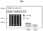
- FIG. 6 is a view showing a window displayed on the screen 315 of the monitor 314. An image 1011 on the left side in the figure is the same as the image 700 shown in FIG.
- step S505 an area to be analyzed on the image is designated in the window 1010 on the screen 315 of the monitor 314. This area is inside the white broken line frame 701 in FIG. 7 and inside the white broken line 1012 in FIG. The dimension along the y direction of the broken-line frame 701 in FIG. 7 is 2000 nm.
- step S506 the three analysis indices displayed in the window 1010 in FIG. 6, that is, 3 ⁇ wig which is an index of the amount of undulation, and 3 ⁇ c which detects the undulation at the center of the line using the undulation index. Select the analysis method to be used this time. In this embodiment, a case where 3 ⁇ wig is selected will be described.
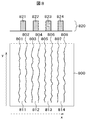
- the edge of the pattern in the frame 701 is calculated as three times ⁇ wig described later as a waviness index. Execute the instruction as follows. First, the edge of the line pattern is extracted from the white band-like region in the broken line frame 701 by image processing. This is shown in FIG. FIG. 8 is a diagram for explaining the calculation process and is not displayed on the screen 315 of the monitor 314.
- edges 801 and 802 are the left and right edges of the line pattern 821 (hereinafter referred to as a line 811 in the top view), and the following 803 and 804 correspond to the pattern 822, and the lines 812 and 805 and 806 correspond to the pattern 823.
- Lines 813, 807 and 808 indicate the left and right edges of the line 814 corresponding to the pattern 824.
- the computer 312 calculates the amount of waviness using the position data of these edges. This procedure is as follows.
- ⁇ wig 2 is calculated for the position data of the left and right edges 801 and 802 of the line 811 using the equations shown in (Equation 1), (Equation 2), (Equation 3), and (Equation 4). Since this is the calculation result of the first line, this amount is denoted as ⁇ 1 wig 2 .
- the arithmetic average of these four quantities is taken, and three times the square root, that is, the average 3 ⁇ wig is displayed in a region near the corner of the image 1011 on the monitor. The number was 5.28 nm.
- step S508 for evaluating the result of the analysis since the allowable limit ⁇ of 3 ⁇ wig is set to 4 nm in advance in the device created using this wafer, NO is determined in S508, and the process proceeds to S510.
- the correlation ⁇ s (m) between the left and right edges of the space between the adjacent line patterns is calculated, the result is displayed on the screen (S509), and the process is terminated.
- This determination can be performed automatically by comparing the measured value with the allowable limit value ⁇ input in advance so that an alarm is sounded when the former exceeds the latter.
- the above-mentioned determination result performed with respect to several wafers can be output to a computer screen.
- Productivity can be improved by sending a wafer that has passed the pass to the next process and passing the failed wafer to the rework process.
- the waviness spectrum can be calculated from the edge position data of each line according to (Equation 5). Thus, if there is a characteristic period of undulation, it can be grasped.
- this process performs self-aligned double patterning (SADP) twice, in which a film is attached on both sides of the formed line pattern, the original line pattern is removed, and the part added as a film is regarded as a new line pattern. Since it was created repeatedly, it was pointed out that the LER of the pattern formed first may be the cause of undulation.
- SADP self-aligned double patterning
- the average value of ⁇ s (m) can be reduced by improving the introduction of a material having a low LER during the first line pattern formation of SADP based on the first table result, and the waviness ⁇
- the wig itself could be made sufficiently small, and the number of rejected wafers could be halved.
- ⁇ Modification 1> As a first modification of the first embodiment, a case where evaluation is performed using ⁇ c instead of swell evaluation index ⁇ wig will be described.
- ⁇ s (m) is calculated in S510 in order to identify the cause of swell.
- the index ⁇ c (m, m + 1) obtained by using (Equation 9) (Equation 10) is used instead of ⁇ s (m)
- the calculation time is long but the reproducibility is high. Measurement can be performed. In this case, it becomes easy to identify the process that causes the swell, and the yield can be improved by taking measures against the cause process.
- the evaluation result is fed back to the process of forming the pattern, A pattern having a desired shape can be stably formed.
- FIG. 9 A second embodiment of the present invention will be described below with reference to FIGS.
- the screen shown in FIG. 6 is used when measuring the overlay error between the line pattern 901 and the lower layer pattern 903 formed in parallel with the upper layer line pattern 901.
- 3 ⁇ c above By selecting 3 ⁇ c above and calculating this value, the overlay deviation that can occur in the actual pattern is correctly predicted, and the pass / fail judgment of the pattern is made.
- the processing flow in the present embodiment is basically the same as the processing flow of FIG. 5 described in the first embodiment.
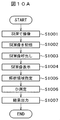
- the flow of processing in the present embodiment will be described with reference to FIG. 10A.
- a target region for calculating an interlayer overlay error is imaged with an SEM (S1001), and this SEM image is stored in the data storage device 313 (S1002).
- S1003 a target image for calculating an interlayer overlay error is called on the monitor (S1003) and displayed on the monitor 314 (S1004).
- a schematic diagram 900 of this image is shown in FIG.
- the horizontal dimension in this figure is 300 nm, and the dimension along the line is 2560 nm. Similar to the first embodiment, this embodiment also shows binarization. In order to facilitate understanding, the corresponding pattern cross-sectional structure 910 is shown at the top.
- a schematic diagram 900 is displayed on the screen 315 of the monitor 314 instead of the image 1011 illustrated in FIG. 6 described in the first embodiment.
- This pattern includes a line pattern 903 formed of a first conductive material on a substrate (not shown), and a layer 902 formed by depositing an insulator formed so as to cover the line pattern 903 is formed.
- the line pattern 901 made of the second conductive material is formed thereon.
- the SEM image of the line pattern 901 only the vicinity of the edge of the pattern looks white, and the SEM image of the line pattern 903 looks white as a whole.
- the display of the lower layer of the line pattern 903 is omitted.
- the measurement object is the interval between the line patterns 901 and 903, which is indicated by D in the figure.
- the difference between the measured value and the design value of 55 nm is the difference between the pattern uppermost layer in which the line pattern 901 is formed and the layer in which the line pattern 903 is formed. This is the amount of misalignment.
- step S1005 frames 904 and 905 shown by white broken lines as shown in FIG. 9 are set on the image 900 displayed on the monitor 314 in order to measure the value of D.
- execution step S1006 the distance D between the centers of the line patterns 901 and 903 is measured on the image 900 as shown in FIG. 9 displayed on the monitor 314 with frames 904 and 905 indicated by white broken lines. Run the recipe. As a result, it is assumed that the obtained values of D are 59 nm and 51 nm. Further, it is assumed that the same process is performed for the same nine design spots of the same sample, and statistical processing is performed on a total of 20 values obtained.
- the average value is 56.2 nm and the standard deviation of the distribution is 2.5 nm. From this, it is determined that the overlay deviation amount this time is +1.2 nm and the measurement error (three times the standard deviation) is 7.5 nm. In the case of this example, since the error is large, it is necessary to urgently perform measurement using an optical device. As a result, the deviation amount was the same as +1.2 nm and the measurement error was only 0.5 nm.
- step S10001 the above-described image 900 shown in FIG. 9 is called and displayed (S10002).
- step S10003 an area to be analyzed is selected as in 906, and the edge of the uppermost line pattern is extracted. The extracted edge is shown in FIG. The length of the extracted line edge in the y direction is 2000 nm.
- S10005 using the position data of the line left edge 1101 and the position data of the right edge 1102 shown in FIG. 11, (Equation 6) and (Equation 7) are applied, and ⁇ c 2 is calculated and output. (S10006) and the process ends.
- an average ⁇ c 2 is measured in advance with the apparatus shown in FIG. 4, and the value obtained by subtracting the square root from the original allowable overlay deviation is defined as the optical overlay deviation target value ⁇ , and then the overlay is obtained.
- the deviation can be evaluated by an optical measuring device. In the evaluation by the optical measuring device, the observation object is rejected when a value larger than the optical overlay deviation target value ⁇ is obtained.
- ⁇ c (m, m + 1) calculated from a set of two adjacent lines is calculated for multiple line sets, and the process that causes the swell is identified from the distribution and countermeasures are taken. Improved yield.
- an instruction was sent from the computer 312 to the CD-SEM control system 311 to move the wafer 307 into the apparatus.
- a silicon line pattern is formed on the wafer 307 by etching.
- the stage was moved and adjusted so that the line pattern group was in the observation field.
- the lenses 304 and 306 and the deflector 305 were electrically adjusted, and a top view image of the pattern was obtained by a signal from the computer 312.
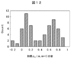
- the sample used in this example contained two or more lines in the image. From the edge position data of this line pattern, ⁇ c (m, m + 1) represented by (Equation 9) was calculated. Where m is the line number. From an image containing N lines, this index can be calculated as N-1. Taking 20 images within the pattern area designed to form the same dimension, and calculating the correlation coefficient ⁇ c (m, m + 1) of the center position fluctuation between the lines, the values are all 60 pieces were obtained.
- FIG. 12 shows the distribution as a histogram. In this graph, there are two peaks, the position where the above-mentioned correlation coefficient is about 0.1-0.2 and the vicinity of 0.7.
Landscapes
- Physics & Mathematics (AREA)
- Electromagnetism (AREA)
- General Physics & Mathematics (AREA)
- Engineering & Computer Science (AREA)
- Computer Vision & Pattern Recognition (AREA)
- Chemical & Material Sciences (AREA)
- Analytical Chemistry (AREA)
- Length-Measuring Devices Using Wave Or Particle Radiation (AREA)
- Testing Or Measuring Of Semiconductors Or The Like (AREA)
Abstract
Description
対象パターンの寸法が100nm以下にまで微細化されてきたため、前述の検査は、電子顕微鏡観察によって行われることが多い。微細なパターンに対して有効な検査方法は、走査型電子顕微鏡(Scanning Electron Microscope:SEM)によって得られるパターン上方からの観察画像を解析することである。但しパターンの寸法が数百nm程度あるいはそれ以上であれば、レーザー顕微鏡を用いて上方から、同様に観察・解析してもよい。
SEM、レーザー顕微鏡、いずれを用いる場合であっても、観察するだけではパターンを精確に検知することができず、また、生産管理に応用することもできない。上方からの観察画像に対して解析を行って、パターンの良否判定を可能にする指標を算出することが必要になる。これまでは、デバイスパターンの中でも製品性能管理上重要なパターンの寸法をCritical Dimension、即ちCDと呼び、それを指標としてきた。しかしパターンの微細化に伴い、単なる平均的なCDだけではなく、ラインパターンエッジの微小な凹凸(Line-edge roughness、即ちLER)が引き起こすライン幅の局所的な変動(Linewidth roughness、即ちLWR)なども定量化し指標に用いる必要が生じた。CDが設計どおりであっても、LWRが大きければデバイスの性能が不十分になるからである。これについては非特許文献1に詳しく記述されている。
しかしこのうねりは、これまでのCD計測でもLWR計測でも検知できない。うねりがあってもなくてもCDやLWRは変わらないからである。LER計測で検知することができるが、その場合でもレジスト材料の不均一性や現像工程でランダムに自然発生する、ラインの左右が同期していない通常のLERと区別することができない。この現象を取り扱っている例としては非特許文献1が挙げられる。この文献の中では、ラインパターンの寸法値がある値以下になるとこのうねりが見られることから、パターン形成プロセス条件に対して、うねりが起こる最大パターン寸法を指標とし、その寸法値が小さいほど、よいプロセスだという評価をしている。
ラインパターンのうねりの程度を定量化する試みとして、非特許文献2に示すLER、LWR、SWR(Space width roughness)を組み合わせた指標による評価方法が提案されている。
上記の他に、LERの原因を探索する目的で、ライン左右のエッジ形状の相関をとる、という手法が提案された。この内容は特許文献1に記載されている。
まず、ラインパターンのトップビュー観察画像から、1本のラインの左右のエッジの位置を抽出する。抽出されたエッジのトップビュー観察画像100の例をその断面の模式図103と共に図1に示す。x、y、z軸は、図中に示したように設定する。ラインパターンの左側のエッジをそのx座標の集合{x(L,i)|i=1,2,…n}, 右側のエッジをそのx座標の集合{x(R,i)|i=1,2,…n}で表す。但し図1中ではエッジ点を直線でつないで折れ線として表示している(101、102)。L,Rはそれぞれ左、右を表しており、nはエッジを表す点の総数である。なお、エッジ点のy方向の間隔をΔyとする。また、左エッジのx座標の平均値をxL、右エッジのx座標の平均値をxRとする。エッジ点の位置を表す変数はx、y座標とも単位をnmとする。

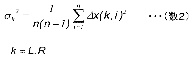

これらの量を使い、ラインの左右のエッジ位置変動のうち、左右に共通している部分の大きさを(数4)のようにして求めることができる。






以上に説明した半導体デバイスのラインパターン形成プロセスを経てウェハ上に形成されたラインパターンのうねりをSEM画像を用いて評価する方法について、図3のフロー図を用いて説明する。
また、S306の工程において、うねり量の指標として3σcを選択した場合、S314に進み、(数6)を用いてラインパターンの中心位置座標を求め、(数7)に従ってその分布を求め(S315)、さらにその値からライン中心位置変動量3σcを計算する。
次にこの3σcの値が予め設定しておいた基準値βと小さいかをチェックする(S317)。小さければ(S317でYESの場合)、このラインパターンのうねりは十分小さいとして、うねり指標3σcを出力して(S350)、終了する。
一方、うねり指標3σcがβと同じかそれ以上であった場合(S317でNOの場合)には、S313により『この観察対象のうねりが大きく、発生の原因を究明するために同期性の評価をさらに行うべきである』という情報を、出力すべきデータに加えた後、出力する(S350)。
図7は本実施例で観察されたラインパターンのトップビュー画像を二値化し白黒表示させた図で、S504でモニタ314の画面315上に表示される画像700である。この700が表す実際の画像は濃淡のあるモノクロ画像であるがここでは簡便のためそれを二値化している。図7の画像700のサイズは、x軸方向が450nm、y軸方向が2560nmである。なお、図7では画像700内の凹凸部分がわかるように、断面図710を同じx軸(ラインパターン711-714に垂直な方向)に沿って表示している。白い帯状の領域702はラインパターン711-714のエッジ近傍を示している。図6は、モニタ314の画面315に表示されたウインドウを示した図で。図中左側にある画像1011は図7内に示されている画像700と同じものである。
パターンエッジの抽出とともにコンピュータ312は、これらのエッジの位置データを用いて、うねりの量を計算する。この手順は以下のとおりである。まずライン811の左右のエッジ801と802の位置データに対して、(数1)(数2)(数3)(数4)に示した式を用いて、σwig 2を算出する。これは1番目のラインの計算結果であるから、この量をσ1wig 2と記す。同様のことをライン812、813、814に対して実施し、σwig 2を求め、σ2wig 2、σ3wig 2、σ4wig 2、とする。これら四つの量の算術平均をとり、その平方根の3倍、即ち平均の3σwigを、モニタ上の画像1011の角に近い領域に表示する。その数字は5.28nmであった。
なお、この判定は、実測値と予め入力していた許容限度値αとを比較し前者が後者を超えた場合に警報が鳴るようにすることで、自動で実施することができる。あるいは、複数のウエハに対して行った上述の判定結果をコンピュータ画面に出力することができる。合格判定だったウエハを次工程に送り、不合格だったウエハをリワーク工程にまわすことで、生産性を向上させることができる。各ラインのエッジ位置データから(数5)に従い、うねりのスペクトルを算出することができる。これにより、うねりの特徴的な周期があれば、それを把握することができる。
実施例1の変形例1として、うねり評価指標をσwigに替えてσcを用いて評価する場合について説明する。上記のうねり評価指標としてσwigを用いた例では、うねりの原因を特定するためにS510においてρs(m)を算出したが、観察対象が帯電するなどして常に一方のエッジにノイズが大きい場合などは、ρs(m)の代わりに(数9)(数10)を用いて得られる指標のρc(m,m+1)を用いると、計算時間は長くかかるが高い再現性で計測を行うことができる。この場合、うねり発生の原因となる工程を同定することが容易になり、原因となる工程を対策することで歩留まりを向上させることができる。
本実施例における処理の流れは、基本的に実施例1で説明した図5の処理フローと同じである。本実施例における処理の流れを、図10Aを用いて本実施例の処理の流れを説明する。
先ず、層間重ね合わせ誤差を算出する対象領域をSEMで撮像し(S1001),このSEM像をデータ記憶装置313に記憶する(S1002)。次に、このデータ記憶装置313に記憶させた画像の中から、モニタ上に層間重ね合わせ誤差を算出する対象画像を呼び出して(S1003)、モニタ314上に表示させる(S1004)。この画像の模式図900を図9に示す。この図の水平方向の寸法は300nm、ラインに沿った方向の寸法は2560nmである。第一の実施例と同様に、本実施例においても二値化させて示している。また、理解しやすくするために、対応するパターン断面構造910を上部に示している。本実施例においては、モニタ314の画面315上には、実施例1で説明した図6の画像1011に替って、模式図900が表示される。
次に、実行ステップS1006において、モニタ314に表示された図9に示すような画像900の上で、白い破線で示した枠904及び905でラインパターン901と903の中心同士の距離Dを測定するレシピを実行する。その結果、得られたDの値が59nmと51nmとであったとする。さらに同じサンプルの同じ設計スポット9箇所について同様のことを行い、得られた合計20個の値の統計処理を行い、その平均値が56.2nm、分布の標準偏差が2.5nmであったとする。ここから、今回の重ね合わせずれ量は+1.2nm、計測誤差(標準偏差の3倍)が7.5nm、と判断される。この例の場合には、誤差が大きいため急遽別途光学装置による計測を実施する必要がある。その結果、ずれ量が+1.2nmと同じでありかつ計測誤差がわずか0.5nmとなった。
まず、S10001で、上述の図9に示す画像900を呼び出し、表示させる(S10002)。さらにS10003で、分析する領域を906のように選択し、最上層のラインパターンのエッジを抽出する。抽出されたエッジを図11に示す。抽出されたラインエッジのy方向の長さは2000nmである。次に、S10005によって、図11に図示されたライン左エッジ1101の位置データと右エッジ1102の位置データを用いて、(数6)(数7)を適用し、σc 2を算出し、出力し(S10006)終了する。これを同様に他の9 箇所のスポットの画像に適用し、σc 2を算出し、合計10個の値の平均値を求め、さらに平方根をとって3倍したところ(3σc)、7.2nmとなった。
この値は、初めに算出された計測誤差7.5nmと非常に近く、誤差と判断された計測値ばらつきの殆どが、うねりによるパターン自身の局所的な位置ずれであるということが明らかにになった。このことから図4に示す装置を用いての重ね合わせずれ測定には問題ないことが判ったため、検査装置の使用は続行した。これにより、検査工程の変更が不要になったため、装置入れ替えによる生産の遅延と費用の発生が回避された。
同時に、パターンのうねりが原因で下層との位置ずれが生じているというプロセス上の問題が明らかになり、これに対処することで歩留まりが向上した。
逆に、予め平均的なσc 2を図4に示す装置で計測しておき、その平方根を本来の重ね合わせずれの許容値から差し引いたものを光学重ね合わせずれターゲット値βとし、その後重ね合わせずれは光学計測装置で評価することが可能である。光学計測装置での評価では、光学重ね合わせずれターゲット値βよりも大きな値が出た場合に観察対象を不合格とする。
まず、コンピュータ312から入力してCD-SEMの制御系311に命令を送り、ウエハ307を装置内に移動した。ウエハ307には、エッチング加工によりシリコンのラインパターンが形成されている。次に、ステージを移動してラインパターン群が観察視野に入るよう調整した。次にレンズ304及び306と偏向器305を電気的に調整し、コンピュータ312からの信号によりパターンのトップビュー画像を取得した。本実施例で使用した試料には、画像にはラインが2本以上含まれていた。このラインパターンのエッジ位置データから、(数9)で表されるρc(m,m+1)を算出した。ここでmはラインの番号である。ラインがN本含まれている画像からはこの指標はN-1個計算することができる。
同じ寸法に形成されるよう設計されているパターン領域内で20箇所の画像を撮り、ライン間の中心位置変動の相関係数ρc(m,m+1)を計算したところ、値は全部で60個得られた。この分布をヒストグラムにしたところ、図12のようになった。このグラフには、前述の相関係数が0.1-0.2程度の位置と、0.7近傍と、二つのピークがある。これは相関の強いラインのセットと、弱いラインのセットがほぼ半分ずつある、という結果を意味している。このパターンの形成工程でSAPDが2回実施されていたことから、最初のパターンのLERが転写されたものと予測することができた。そこでプロセスを見直し、最初のパターン形成後にLER低減プロセスを導入したところ、うねり自体を0.5nm程度に低減され、歩留まりを向上することができた。
なお、ρc(m,m+1)の代わりにρs(m)を用いる方法もある。レジスト材料起因のランダムなLERが小さい場合はρs(m)のほうが高い感度でうねりの同期性を検出できる。
また、ρc(m,m+1)の代わりに3σLL(m,m+1)を用いる方法もある。この場合、同期する成分をライン中心の変動量として距離の単位で表すことができるため、単なる同期の有無ではなくその程度をモニタリングする際に適している。
Claims (18)
- 試料に荷電粒子線を照射し得られた画像における前記試料のラインパターンの形状を評価する方法であって、
前記ラインパターンの輪郭の両端のエッジ点を抽出する抽出工程と、
前記ラインパターンが延在する方向において、前記両端のエッジ点の変動量を算出する変動量算出工程と、
前記ラインパターンが延在する方向において、前記両端のエッジ点の幅の変動量を算出する幅変動量算出工程と、
前記両端のエッジ点の変動量と前記両端のエッジ点の幅の変動量との差分を算出する差分算出工程と、を有することを特徴とするラインパターンの形状評価方法。 - 請求項1に記載のラインパターンの形状を評価する方法であって、
前記両端のエッジ点が含まれた指定領域を設定する領域設定工程をさらに有し、
前記差分算出工程は、前記指定領域における複数のエッジ点の平均値もしくは分散値に基づいて実行されることを特徴とするラインパターンの形状評価方法。 - 請求項1に記載のラインパターンの形状を評価する方法であって、
前記ラインパターンの輪郭の両端に沿った方向における変動である第1及び第2パワースペクトルを算出するスペクトル算出工程とを有し、
前記差分算出工程は、前記第1及び第2パワースペクトルに基づいて実行されることを特徴とするラインパターンの形状評価方法。 - 試料に荷電粒子線を照射し得られた画像における前記試料のラインパターンの形状を評価する方法であって、
前記ラインパターンの輪郭の両端のエッジ点を抽出する抽出工程と、
前記両端のエッジ点に基づき前記ラインパターンの中心点を算出する中心点算出工程と、
前記ラインパターンが延在する方向において、前記抽出工程と前記中心点算出工程とを複数回実行する実行工程と、
前記実行工程にて算出された複数の前記ラインパターンの中心点の分散値を算出する分散値算出工程とを有することを特徴とするラインパターンの形状評価方法。 - 請求項4に記載のラインパターンの形状を評価する方法であって、
荷電粒子線装置により得られたパターン重ね合わせずれ量計測のばらつきの分散値と、前記分散値とに基づき、重ね合わせずれ計測における誤差の分散値を算出する重ね合わせずれ算出工程を有することを特徴とするラインパターンの形状評価方法。 - 試料に荷電粒子線を照射し得られた画像における前記試料のラインパターンの形状を評価する方法であって、
前記ラインパターンの輪郭のエッジ点を抽出する抽出工程と、
前記ラインパターンが延在する方向において、前記ラインパターンの輪郭に沿った方向における前記エッジ点の変動量を算出する変動量算出工程と、
前記変動量と前記ラインパターンに隣り合うラインパターンのエッジ点の変動量との類似度を算出する類似度算出工程と、を有することを特徴とするラインパターンの形状評価方法。 - 請求項6に記載のラインパターンの形状を評価する方法であって、
前記類似度算出工程は、前記ラインパターンの第1の側のエッジ点の変動量と、前記ラインパターンに隣り合うラインパターンの前記第1の側とは異なる第2の側のエッジ点の変動量との類似度を算出することを特徴とするラインパターンの形状評価方法。 - 請求項6に記載のラインパターンの形状を評価する方法であって、さらに、
前記両端のエッジ点に基づき前記ラインパターンの中心点を算出する中心点算出工程と、
前記ラインパターンが延在する方向において、前記抽出工程と前記中心点算出工程とを複数回実行する実行工程と、
前記実行工程を隣接する他のラインパターンにおいても実行する隣接パターン実行工程とを有し、
前記類似度算出工程は、前記実行工程から得られたラインパターンの中心位置の変動と、隣接パターン実行工程から得られた前記隣接する他のラインパターンの中心位置の変動との類似度を算出することを特徴とするラインパターンの形状評価方法。 - 試料に荷電粒子線を照射し得られた画像における前記試料のラインパターンの形状を評価する方法であって、
前記ラインパターンの輪郭の両端のエッジ点を抽出する抽出工程と、
前記両端のエッジ点に基づき前記ラインパターンの中心点を算出する中心点算出工程と、
前記ラインパターンが延在する方向において、前記抽出工程と前記中心点算出工程とを複数回実行し前記ラインパターンの中心点の変動量を算出する実行工程と、
前記実行工程を隣接する他のラインパターンにおいても実行する隣接パターン実行工程と、
前記ラインパターンの中心点の変動量と前記他のラインパターンの中心点の変動量とに基づき、前記ラインパターンと前記他のラインパターンとにおいて類似している変動量を算出する類似変動量算出工程とを有することを特徴とするラインパターンの形状評価方法。 - 試料に荷電粒子線を照射し得られた画像が記憶された画像記憶部と、
前記画像記憶部に記憶された前記画像におけるラインパターンの輪郭の両端のエッジ点を抽出する抽出部と、
前記ラインパターンが延在する方向において、前記両端のエッジ点の変動量を算出する変動量算出部と、
前記ラインパターンが延在する方向において、前記両端のエッジ点の幅の変動量を算出する幅変動量算出部と、
前記両端のエッジ点の変動量と前記両端のエッジ点の幅の変動量との差分を算出する差分算出部と、を有することを特徴とするラインパターンの形状評価装置。 - 請求項10に記載のラインパターンの形状を評価する装置であって、
前記両端のエッジ点が含まれた指定領域を設定する領域設定部をさらに有し、
前記差分算出部は、前記指定領域における複数のエッジ点の平均値もしくは分散値に基づいて実行されることを特徴とするラインパターンの形状評価装置。 - 請求項10に記載のラインパターンの形状を評価する装置であって、
前記ラインパターンの輪郭の両端に沿った方向における変動である第1及び第2パワースペクトルを算出するスペクトル算出部をさらに有し、
前記差分算出部は、前記第1及び第2パワースペクトルに基づいて実行されることを特徴とするラインパターンの形状評価装置。 - 試料に荷電粒子線を照射し得られた画像が記憶された画像記憶部と、
前記画像記憶部に記憶された前記画像におけるラインパターンの輪郭の両端のエッジ点を抽出する抽出部と、
前記両端のエッジ点に基づき前記ラインパターンの中心点を算出する中心点算出部と、
前記ラインパターンが延在する方向において、前記抽出部と前記中心点算出部との処理を複数回実行する実行部と、
前記実行部にて算出された複数の前記ラインパターンの中心点の分散値を算出する分散値算出部とを有することを特徴とするラインパターンの形状評価装置。 - 請求項13に記載のラインパターンの形状を評価する装置であって、
荷電粒子線装置により得られたパターン重ね合わせずれ量計測のばらつきの分散値と、前記分散値とに基づき、重ね合わせずれ計測における誤差の分散値を算出する重ね合わせずれ算出部を有することを特徴とするラインパターンの形状評価装置。 - 試料に荷電粒子線を照射し得られた画像が記憶された画像記憶部と、
前記画像記憶部に記憶された前記画像におけるラインパターンの輪郭の両端のエッジ点を抽出する抽出部と、
前記ラインパターンが延在する方向において、前記ラインパターンの輪郭に沿った方向における前記エッジ点の変動量を算出する変動量算出部と、
前記変動量と前記ラインパターンに隣り合うラインパターンのエッジ点の変動量との類似度を算出する類似度算出部と、を有することを特徴とするラインパターンの形状評価装置。 - 請求項15に記載のラインパターンの形状を評価する装置であって、
前記類似度算出部は、前記ラインパターンの第1の側のエッジ点の変動量と、前記ラインパターンに隣り合うラインパターンの前記第1の側とは異なる第2の側のエッジ点の変動量との類似度を算出することを特徴とするラインパターンの形状評価装置。 - 請求項15に記載のラインパターンの形状を評価する装置であって、さらに、
前記両端のエッジ点に基づき前記ラインパターンの中心点を算出する中心点算出部と、
前記ラインパターンが延在する方向において、前記抽出部と前記中心点算出部との処理を複数回実行する実行部と、
前記実行部における処理を隣接する他のラインパターンにおいても実行する隣接パターン実行部とを有し、
前記類似度算出部は、前記実行部から得られたラインパターンの中心位置の変動と、隣接パターン実行部から得られた前記隣接する他のラインパターンの中心位置の変動との類似度を算出することを特徴とするラインパターンの形状評価装置。 - 試料に荷電粒子線を照射し得られた画像が記憶された画像記憶部と、
前記画像記憶部に記憶された前記画像におけるラインパターンの輪郭の両端のエッジ点を抽出する抽出部と、
前記両端のエッジ点に基づき前記ラインパターンの中心点を算出する中心点算出部と、
前記ラインパターンが延在する方向において、前記抽出部と前記中心点算出部との処理を複数回実行し前記ラインパターンの中心点の変動量を算出する実行部と、
前記実行部の処理を隣接する他のラインパターンにおいても実行する隣接パターン実行部と、
前記ラインパターンの中心点の変動量と前記他のラインパターンの中心点の変動量とに基づき、前記ラインパターンと前記他のラインパターンとの類似している箇所における変動量を算出する類似変動量算出部とを有することを特徴とするラインパターンの形状評価装置。
Priority Applications (2)
| Application Number | Priority Date | Filing Date | Title |
|---|---|---|---|
| US14/897,609 US9658063B2 (en) | 2013-06-11 | 2014-05-27 | Method and device for line pattern shape evaluation |
| KR1020157033545A KR101810436B1 (ko) | 2013-06-11 | 2014-05-27 | 라인 패턴의 형상 평가 방법 및 그 장치 |
Applications Claiming Priority (2)
| Application Number | Priority Date | Filing Date | Title |
|---|---|---|---|
| JP2013-122614 | 2013-06-11 | ||
| JP2013122614A JP6129651B2 (ja) | 2013-06-11 | 2013-06-11 | ラインパターンの形状評価方法及びその装置 |
Publications (1)
| Publication Number | Publication Date |
|---|---|
| WO2014199820A1 true WO2014199820A1 (ja) | 2014-12-18 |
Family
ID=52022119
Family Applications (1)
| Application Number | Title | Priority Date | Filing Date |
|---|---|---|---|
| PCT/JP2014/064006 Ceased WO2014199820A1 (ja) | 2013-06-11 | 2014-05-27 | ラインパターンの形状評価方法及びその装置 |
Country Status (5)
| Country | Link |
|---|---|
| US (1) | US9658063B2 (ja) |
| JP (1) | JP6129651B2 (ja) |
| KR (1) | KR101810436B1 (ja) |
| TW (1) | TWI529388B (ja) |
| WO (1) | WO2014199820A1 (ja) |
Families Citing this family (8)
| Publication number | Priority date | Publication date | Assignee | Title |
|---|---|---|---|---|
| KR102006316B1 (ko) * | 2014-02-17 | 2019-08-01 | 에이에스엠엘 네델란즈 비.브이. | 에지 배치 오차를 결정하는 방법, 검사 장치, 패터닝 디바이스, 기판 및 디바이스 제조 방법 |
| CN109804222B (zh) * | 2016-12-06 | 2021-12-10 | 日本电气硝子株式会社 | 带状玻璃膜的品质检查方法 |
| JP2019039884A (ja) * | 2017-08-29 | 2019-03-14 | 株式会社日立ハイテクノロジーズ | パターン測定方法、及びパターン測定装置 |
| JP7011562B2 (ja) | 2018-09-25 | 2022-01-26 | 株式会社日立ハイテク | パターン形状評価装置、パターン形状評価システム及びパターン形状評価方法 |
| KR102563023B1 (ko) | 2018-11-12 | 2023-08-03 | 주식회사 히타치하이테크 | 결함의 발생을 추정하는 시스템, 및 컴퓨터 가독 매체 |
| JP7310466B2 (ja) * | 2019-09-10 | 2023-07-19 | 株式会社ニューフレアテクノロジー | マルチ荷電粒子ビーム評価方法 |
| EP3862814A1 (en) * | 2020-02-10 | 2021-08-11 | ASML Netherlands B.V. | Multi-step process inspection method |
| KR20260104161A (ko) * | 2023-11-06 | 2026-07-03 | 램 리써치 코포레이션 | 라인 에지 거칠기 (line edge roughness) 메트릭 및 라인 폭 거칠기 (line width roughness) 메트릭 결정 |
Citations (2)
| Publication number | Priority date | Publication date | Assignee | Title |
|---|---|---|---|---|
| JP2003037139A (ja) * | 2001-07-25 | 2003-02-07 | Hitachi Ltd | パターン検査方法及びパターン検査装置 |
| JP2009257937A (ja) * | 2008-04-17 | 2009-11-05 | Hitachi High-Technologies Corp | データ解析装置 |
Family Cites Families (4)
| Publication number | Priority date | Publication date | Assignee | Title |
|---|---|---|---|---|
| JP2004251829A (ja) * | 2003-02-21 | 2004-09-09 | Hitachi High-Technologies Corp | 測長機能を備えた走査形電子顕微鏡およびそれを使用した測長方法 |
| JP2006038779A (ja) * | 2004-07-30 | 2006-02-09 | Hitachi High-Technologies Corp | パターン形状評価方法、評価装置、及び半導体装置の製造方法 |
| JP4801795B2 (ja) * | 2005-01-04 | 2011-10-26 | 株式会社日立ハイテクノロジーズ | パターン形状評価方法及び電子顕微鏡 |
| JP2008116472A (ja) * | 2008-01-07 | 2008-05-22 | Hitachi Ltd | パターン検査方法 |
-
2013
- 2013-06-11 JP JP2013122614A patent/JP6129651B2/ja active Active
-
2014
- 2014-04-10 TW TW103113208A patent/TWI529388B/zh active
- 2014-05-27 WO PCT/JP2014/064006 patent/WO2014199820A1/ja not_active Ceased
- 2014-05-27 KR KR1020157033545A patent/KR101810436B1/ko active Active
- 2014-05-27 US US14/897,609 patent/US9658063B2/en active Active
Patent Citations (2)
| Publication number | Priority date | Publication date | Assignee | Title |
|---|---|---|---|---|
| JP2003037139A (ja) * | 2001-07-25 | 2003-02-07 | Hitachi Ltd | パターン検査方法及びパターン検査装置 |
| JP2009257937A (ja) * | 2008-04-17 | 2009-11-05 | Hitachi High-Technologies Corp | データ解析装置 |
Non-Patent Citations (2)
| Title |
|---|
| GLODDE, M. ET AL.: "Systematic studies on reactive ion etch-induced deformations of organic underlayers", PROCEEDINGS OF SPIE, vol. 7972, 15 April 2011 (2011-04-15), pages 797216-1 - 1 - 797216-8 * |
| WEIGAND, M. ET AL.: "Evaluating spin-on carbon materials at low temperatures for high wiggling resistance", PROCEEDINGS OF SPIE, vol. 8685, 29 March 2013 (2013-03-29), pages 86850R-1 - 1 - 86850R-9 * |
Also Published As
| Publication number | Publication date |
|---|---|
| JP6129651B2 (ja) | 2017-05-17 |
| JP2014240765A (ja) | 2014-12-25 |
| KR20160003087A (ko) | 2016-01-08 |
| US20160123726A1 (en) | 2016-05-05 |
| KR101810436B1 (ko) | 2017-12-20 |
| TWI529388B (zh) | 2016-04-11 |
| TW201508267A (zh) | 2015-03-01 |
| US9658063B2 (en) | 2017-05-23 |
Similar Documents
| Publication | Publication Date | Title |
|---|---|---|
| JP6129651B2 (ja) | ラインパターンの形状評価方法及びその装置 | |
| US10445875B2 (en) | Pattern-measuring apparatus and semiconductor-measuring system | |
| JP3870044B2 (ja) | パターン検査方法及びパターン検査装置 | |
| US8310666B2 (en) | Apparatus of inspecting defect in semiconductor and method of the same | |
| JP2021182162A (ja) | デバイスの特性の予測方法及びシステム | |
| US20080240544A1 (en) | System for creating an inspection recipe, system for reviewing defects, method for creating an inspection recipe and method for reviewing defects | |
| CN110892516B (zh) | 识别晶片上的干扰缺陷的来源 | |
| US9589086B2 (en) | Method for measuring and analyzing surface structure of chip or wafer | |
| US20070105243A1 (en) | Method and apparatus for semiconductor device production process monitoring and method and apparatus for estimating cross sectional shape of a pattern | |
| KR101615843B1 (ko) | 반도체 계측 장치 및 기록 매체 | |
| JP6900252B2 (ja) | パターン検査装置の検査結果の度数分布形状に関する情報を活用する方法 | |
| JP4801795B2 (ja) | パターン形状評価方法及び電子顕微鏡 | |
| JP6492185B2 (ja) | 検査装置 | |
| JP5733011B2 (ja) | 欠陥検査方法、半導体装置の製造方法及び欠陥検査装置 | |
| JP2006319351A (ja) | パターン検査方法及びパターン検査装置 | |
| US20110224934A1 (en) | Evaluating apparatus, evaluating method, and computer program product |
Legal Events
| Date | Code | Title | Description |
|---|---|---|---|
| 121 | Ep: the epo has been informed by wipo that ep was designated in this application |
Ref document number: 14810555 Country of ref document: EP Kind code of ref document: A1 |
|
| ENP | Entry into the national phase |
Ref document number: 20157033545 Country of ref document: KR Kind code of ref document: A |
|
| WWE | Wipo information: entry into national phase |
Ref document number: 14897609 Country of ref document: US |
|
| NENP | Non-entry into the national phase |
Ref country code: DE |
|
| 122 | Ep: pct application non-entry in european phase |
Ref document number: 14810555 Country of ref document: EP Kind code of ref document: A1 |