WO2014196487A1 - 有機半導体膜、その製造方法及びトランジスタ構造 - Google Patents
有機半導体膜、その製造方法及びトランジスタ構造 Download PDFInfo
- Publication number
- WO2014196487A1 WO2014196487A1 PCT/JP2014/064563 JP2014064563W WO2014196487A1 WO 2014196487 A1 WO2014196487 A1 WO 2014196487A1 JP 2014064563 W JP2014064563 W JP 2014064563W WO 2014196487 A1 WO2014196487 A1 WO 2014196487A1
- Authority
- WO
- WIPO (PCT)
- Prior art keywords
- semiconductor film
- organic semiconductor
- film according
- dimensional network
- network structure
- Prior art date
- Legal status (The legal status is an assumption and is not a legal conclusion. Google has not performed a legal analysis and makes no representation as to the accuracy of the status listed.)
- Ceased
Links
Images




Classifications
-
- H—ELECTRICITY
- H10—SEMICONDUCTOR DEVICES; ELECTRIC SOLID-STATE DEVICES NOT OTHERWISE PROVIDED FOR
- H10K—ORGANIC ELECTRIC SOLID-STATE DEVICES
- H10K85/00—Organic materials used in the body or electrodes of devices covered by this subclass
- H10K85/60—Organic compounds having low molecular weight
- H10K85/615—Polycyclic condensed aromatic hydrocarbons, e.g. anthracene
- H10K85/624—Polycyclic condensed aromatic hydrocarbons, e.g. anthracene containing six or more rings
-
- C—CHEMISTRY; METALLURGY
- C07—ORGANIC CHEMISTRY
- C07C—ACYCLIC OR CARBOCYCLIC COMPOUNDS
- C07C13/00—Cyclic hydrocarbons containing rings other than, or in addition to, six-membered aromatic rings
- C07C13/28—Polycyclic hydrocarbons or acyclic hydrocarbon derivatives thereof
- C07C13/32—Polycyclic hydrocarbons or acyclic hydrocarbon derivatives thereof with condensed rings
- C07C13/62—Polycyclic hydrocarbons or acyclic hydrocarbon derivatives thereof with condensed rings with more than three condensed rings
- C07C13/64—Polycyclic hydrocarbons or acyclic hydrocarbon derivatives thereof with condensed rings with more than three condensed rings with a bridged ring system
-
- C—CHEMISTRY; METALLURGY
- C07—ORGANIC CHEMISTRY
- C07C—ACYCLIC OR CARBOCYCLIC COMPOUNDS
- C07C13/00—Cyclic hydrocarbons containing rings other than, or in addition to, six-membered aromatic rings
- C07C13/28—Polycyclic hydrocarbons or acyclic hydrocarbon derivatives thereof
- C07C13/32—Polycyclic hydrocarbons or acyclic hydrocarbon derivatives thereof with condensed rings
- C07C13/70—Polycyclic hydrocarbons or acyclic hydrocarbon derivatives thereof with condensed rings with a condensed ring system consisting of at least two, mutually uncondensed aromatic ring systems, linked by an annular structure formed by carbon chains on non-adjacent positions of the aromatic ring, e.g. cyclophanes
-
- C—CHEMISTRY; METALLURGY
- C07—ORGANIC CHEMISTRY
- C07C—ACYCLIC OR CARBOCYCLIC COMPOUNDS
- C07C2/00—Preparation of hydrocarbons from hydrocarbons containing a smaller number of carbon atoms
- C07C2/76—Preparation of hydrocarbons from hydrocarbons containing a smaller number of carbon atoms by condensation of hydrocarbons with partial elimination of hydrogen
-
- C—CHEMISTRY; METALLURGY
- C08—ORGANIC MACROMOLECULAR COMPOUNDS; THEIR PREPARATION OR CHEMICAL WORKING-UP; COMPOSITIONS BASED THEREON
- C08G—MACROMOLECULAR COMPOUNDS OBTAINED OTHERWISE THAN BY REACTIONS ONLY INVOLVING UNSATURATED CARBON-TO-CARBON BONDS
- C08G61/00—Macromolecular compounds obtained by reactions forming a carbon-to-carbon link in the main chain of the macromolecule
- C08G61/02—Macromolecular compounds containing only carbon atoms in the main chain of the macromolecule, e.g. polyxylylenes
- C08G61/10—Macromolecular compounds containing only carbon atoms in the main chain of the macromolecule, e.g. polyxylylenes only aromatic carbon atoms, e.g. polyphenylenes
-
- H—ELECTRICITY
- H10—SEMICONDUCTOR DEVICES; ELECTRIC SOLID-STATE DEVICES NOT OTHERWISE PROVIDED FOR
- H10K—ORGANIC ELECTRIC SOLID-STATE DEVICES
- H10K71/00—Manufacture or treatment specially adapted for the organic devices covered by this subclass
- H10K71/10—Deposition of organic active material
- H10K71/16—Deposition of organic active material using physical vapour deposition [PVD], e.g. vacuum deposition or sputtering
- H10K71/164—Deposition of organic active material using physical vapour deposition [PVD], e.g. vacuum deposition or sputtering using vacuum deposition
-
- H—ELECTRICITY
- H10—SEMICONDUCTOR DEVICES; ELECTRIC SOLID-STATE DEVICES NOT OTHERWISE PROVIDED FOR
- H10K—ORGANIC ELECTRIC SOLID-STATE DEVICES
- H10K85/00—Organic materials used in the body or electrodes of devices covered by this subclass
- H10K85/60—Organic compounds having low molecular weight
-
- H—ELECTRICITY
- H10—SEMICONDUCTOR DEVICES; ELECTRIC SOLID-STATE DEVICES NOT OTHERWISE PROVIDED FOR
- H10K—ORGANIC ELECTRIC SOLID-STATE DEVICES
- H10K85/00—Organic materials used in the body or electrodes of devices covered by this subclass
- H10K85/60—Organic compounds having low molecular weight
- H10K85/615—Polycyclic condensed aromatic hydrocarbons, e.g. anthracene
- H10K85/625—Polycyclic condensed aromatic hydrocarbons, e.g. anthracene containing at least one aromatic ring having 7 or more carbon atoms, e.g. azulene
-
- C—CHEMISTRY; METALLURGY
- C07—ORGANIC CHEMISTRY
- C07C—ACYCLIC OR CARBOCYCLIC COMPOUNDS
- C07C2523/00—Catalysts comprising metals or metal oxides or hydroxides, not provided for in group C07C2521/00
- C07C2523/38—Catalysts comprising metals or metal oxides or hydroxides, not provided for in group C07C2521/00 of noble metals
- C07C2523/40—Catalysts comprising metals or metal oxides or hydroxides, not provided for in group C07C2521/00 of noble metals of the platinum group metals
- C07C2523/46—Ruthenium, rhodium, osmium or iridium
-
- C—CHEMISTRY; METALLURGY
- C07—ORGANIC CHEMISTRY
- C07C—ACYCLIC OR CARBOCYCLIC COMPOUNDS
- C07C2523/00—Catalysts comprising metals or metal oxides or hydroxides, not provided for in group C07C2521/00
- C07C2523/38—Catalysts comprising metals or metal oxides or hydroxides, not provided for in group C07C2521/00 of noble metals
- C07C2523/48—Silver or gold
- C07C2523/52—Gold
-
- C—CHEMISTRY; METALLURGY
- C07—ORGANIC CHEMISTRY
- C07C—ACYCLIC OR CARBOCYCLIC COMPOUNDS
- C07C2523/00—Catalysts comprising metals or metal oxides or hydroxides, not provided for in group C07C2521/00
- C07C2523/70—Catalysts comprising metals or metal oxides or hydroxides, not provided for in group C07C2521/00 of the iron group metals or copper
- C07C2523/72—Copper
-
- C—CHEMISTRY; METALLURGY
- C07—ORGANIC CHEMISTRY
- C07C—ACYCLIC OR CARBOCYCLIC COMPOUNDS
- C07C2523/00—Catalysts comprising metals or metal oxides or hydroxides, not provided for in group C07C2521/00
- C07C2523/70—Catalysts comprising metals or metal oxides or hydroxides, not provided for in group C07C2521/00 of the iron group metals or copper
- C07C2523/74—Iron group metals
- C07C2523/75—Cobalt
-
- C—CHEMISTRY; METALLURGY
- C07—ORGANIC CHEMISTRY
- C07C—ACYCLIC OR CARBOCYCLIC COMPOUNDS
- C07C2523/00—Catalysts comprising metals or metal oxides or hydroxides, not provided for in group C07C2521/00
- C07C2523/70—Catalysts comprising metals or metal oxides or hydroxides, not provided for in group C07C2521/00 of the iron group metals or copper
- C07C2523/74—Iron group metals
- C07C2523/755—Nickel
-
- C—CHEMISTRY; METALLURGY
- C08—ORGANIC MACROMOLECULAR COMPOUNDS; THEIR PREPARATION OR CHEMICAL WORKING-UP; COMPOSITIONS BASED THEREON
- C08G—MACROMOLECULAR COMPOUNDS OBTAINED OTHERWISE THAN BY REACTIONS ONLY INVOLVING UNSATURATED CARBON-TO-CARBON BONDS
- C08G2261/00—Macromolecular compounds obtained by reactions forming a carbon-to-carbon link in the main chain of the macromolecule
- C08G2261/30—Monomer units or repeat units incorporating structural elements in the main chain
- C08G2261/31—Monomer units or repeat units incorporating structural elements in the main chain incorporating aromatic structural elements in the main chain
- C08G2261/312—Non-condensed aromatic systems, e.g. benzene
-
- C—CHEMISTRY; METALLURGY
- C08—ORGANIC MACROMOLECULAR COMPOUNDS; THEIR PREPARATION OR CHEMICAL WORKING-UP; COMPOSITIONS BASED THEREON
- C08G—MACROMOLECULAR COMPOUNDS OBTAINED OTHERWISE THAN BY REACTIONS ONLY INVOLVING UNSATURATED CARBON-TO-CARBON BONDS
- C08G2261/00—Macromolecular compounds obtained by reactions forming a carbon-to-carbon link in the main chain of the macromolecule
- C08G2261/90—Applications
- C08G2261/92—TFT applications
-
- H—ELECTRICITY
- H10—SEMICONDUCTOR DEVICES; ELECTRIC SOLID-STATE DEVICES NOT OTHERWISE PROVIDED FOR
- H10K—ORGANIC ELECTRIC SOLID-STATE DEVICES
- H10K10/00—Organic devices specially adapted for rectifying, amplifying, oscillating or switching; Organic capacitors or resistors having potential barriers
- H10K10/40—Organic transistors
- H10K10/46—Field-effect transistors, e.g. organic thin-film transistors [OTFT]
- H10K10/462—Insulated gate field-effect transistors [IGFETs]
- H10K10/466—Lateral bottom-gate IGFETs comprising only a single gate
-
- H—ELECTRICITY
- H10—SEMICONDUCTOR DEVICES; ELECTRIC SOLID-STATE DEVICES NOT OTHERWISE PROVIDED FOR
- H10K—ORGANIC ELECTRIC SOLID-STATE DEVICES
- H10K10/00—Organic devices specially adapted for rectifying, amplifying, oscillating or switching; Organic capacitors or resistors having potential barriers
- H10K10/40—Organic transistors
- H10K10/46—Field-effect transistors, e.g. organic thin-film transistors [OTFT]
- H10K10/462—Insulated gate field-effect transistors [IGFETs]
- H10K10/484—Insulated gate field-effect transistors [IGFETs] characterised by the channel regions
Definitions
- the present invention relates to an organic semiconductor film, a manufacturing method thereof, and a transistor structure, and more particularly, to an organic semiconductor film having a pseudo graphene structure.
- metal for example, Cu
- Cu is used for the wiring of the transistor structure.
- the conduction electrons are affected by inelastic scattering at the interface due to the thin wire effect. Since it receives strongly, there exists a problem that wiring becomes high resistance.
- graphene has an extremely long mean free path and high mobility, and when applied to a fine wiring structure, the possibility of realizing a low resistance wiring exceeding Cu has been shown (for example, non-patent literature). 1). Therefore, in the next-generation transistor structure that needs to realize a finer laminated structure and wiring structure, it has been studied to use graphene instead of Cu as a wiring film.
- a CVD method for example, thermal CVD method or plasma CVD method
- the substrate surface is covered with a catalytic metal layer
- the catalytic metal layer is activated, and then decomposed from the source gas.
- the carbon atoms are dissolved in the activated catalytic metal layer and recrystallized. That is, since graphene can be directly generated on a substrate having a relatively large area, the CVD method can be easily adapted to an existing semiconductor device formation process.
- a plasma CVD method is mainly used in which the substrate gas only needs to be heated to a relatively low temperature, for example, 600 ° C. or lower by decomposing the source gas with plasma.
- a hydrocarbon gas is used as a source gas, plasma is generated from the hydrocarbon gas, and carbon radicals in the plasma are dissolved in the catalyst metal layer (see, for example, Patent Document 1).
- the graphene nanomesh is formed by forming the graphene nanoribbons by processing the thin-film graphene generated by the above-mentioned plasma CVD method into nanoscale strips, or by drilling holes according to a predetermined pattern It has been proposed to form a narrow portion and generate a band gap by the quantum size effect (see, for example, Non-Patent Documents 2 to 4). For example, it has been reported that in order to generate a band gap of 500 meV by the quantum size effect, it is necessary to process the width of the graphene nanoribbon to 8 nm or less (for example, see Non-Patent Document 5).
- An object of the present invention is to provide an organic semiconductor film that can reliably obtain a desired band gap, a method for manufacturing the same, and a transistor structure.
- the pseudo graphene structure is preferably composed of a single layer of the two-dimensional network structure.
- the pseudo graphene structure is preferably composed of a single layer of the two-dimensional network structure.
- the two-dimensional network structure in the organic semiconductor film according to claim 1 or 2 has a plurality of 5,5 ′, 5 ′′, 5 ′ ′′, 5 ′′ ′′, 5 ′ ′′ ′′-hexabromocyclohexa-m-phenylene (hereinafter simply referred to as “CHP”) is formed by polymerizing each other, and the CHP is an organic semiconductor having bromine in the side chain.
- CHP 5,5 ′, 5 ′′, 5 ′ ′′, 5 ′′ ′′, 5 ′ ′′ ′′-hexabromocyclohexa-m-phenylene
- the two-dimensional network structure is preferably formed by vapor-depositing the plurality of CHPs on the surface of a single crystal metal having catalytic ability.
- the surface of the single crystal metal is preferably constituted by a (111) plane in the face-centered cubic lattice.
- the surface of the single crystal metal is preferably constituted by a (0001) plane in the hexagonal close-packed structure.
- the two-dimensional network structure is preferably formed by depositing the plurality of CHPs on the surface of a polycrystalline metal containing grains having catalytic ability.
- the surface of the grain is composed of (111) planes in the face-centered cubic lattice.
- the surface of the grain is constituted by a (0001) plane in the hexagonal close-packed structure.
- the two-dimensional network structure in the organic semiconductor film according to claim 3 or 4 has a plurality of 2,3,6,7,10,11-hexabromotriphenylene.
- HBTP a method for producing an organic semiconductor film formed by polymerizing each other
- the two-dimensional network structure is preferably formed by evaporating the plurality of HBTPs on a surface of a single crystal metal having catalytic ability.
- the surface of the single crystal metal is preferably constituted by a (111) plane in the face-centered cubic lattice.
- the surface of the single crystal metal is preferably constituted by a (0001) plane in the hexagonal close-packed structure.
- the two-dimensional network structure is preferably formed by evaporating the plurality of HBTPs on the surface of a polycrystalline metal containing grains having catalytic ability.
- the surface of the grain is composed of (111) planes in the face-centered cubic lattice.
- the surface of the grain is constituted by a (0001) plane in the hexagonal close-packed structure.
- a transistor structure using the organic semiconductor film according to any one of claims 1 to 4 as a channel is provided.
- the organic semiconductor film has a pseudo graphene structure in which a two-dimensional network structure of molecules of an organic compound is continuously formed.
- the two-dimensional network structure is used for spontaneous order formation of molecules of the organic compound. Therefore, the shape of the neck or end of the two-dimensional network structure is uniquely determined according to the shape of the molecule of the organic compound and the modifying group.
- the neck width can be set to the ⁇ order. That is, since the neck having a width of ⁇ order can be uniquely formed based on the spontaneous order formation of the molecules of each organic compound, a desired band gap can be reliably obtained.
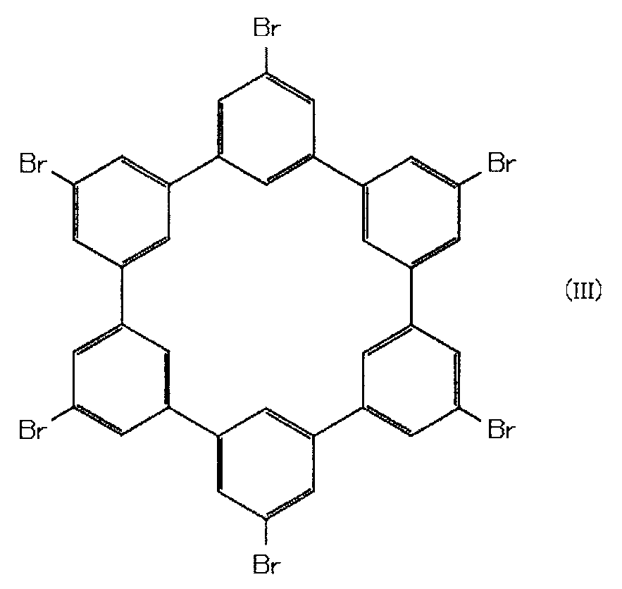
- the organic semiconductor film according to the present embodiment is manufactured from CHP which is a molecule of an organic compound represented by the following formula (III).
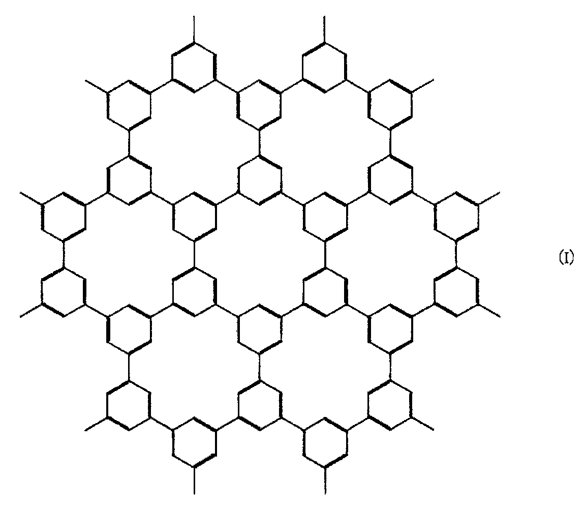
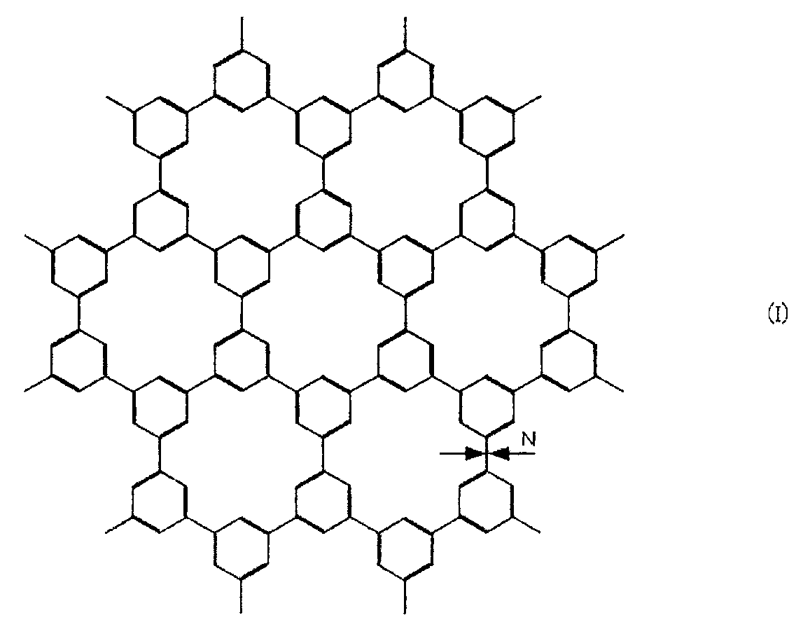
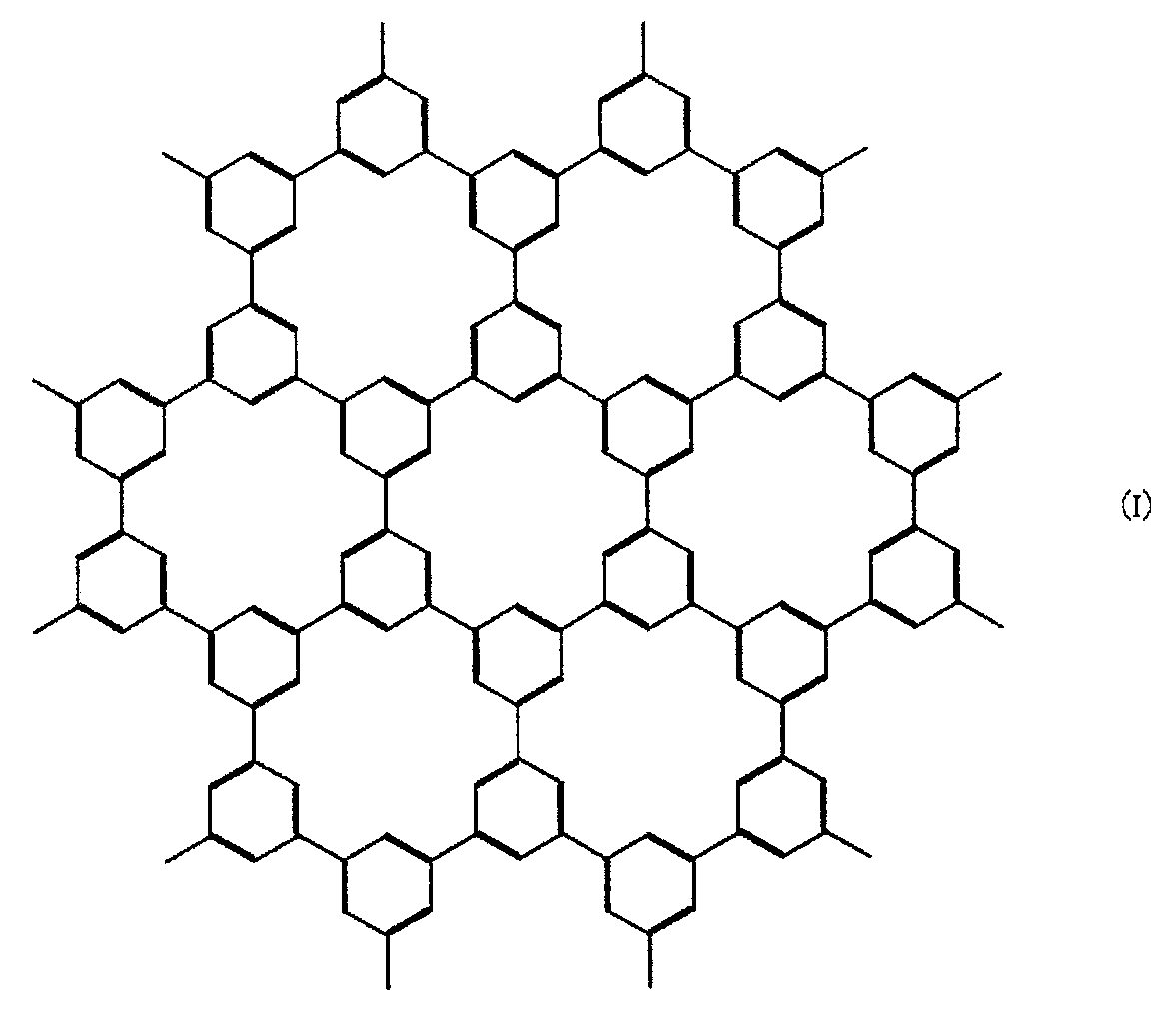
- the CHP represented by the above formula (III) has bromine as a halogen in the side chain, and in this embodiment, the CHP represented by the plurality of the above formula (III) is represented by the following formula (I). A two-dimensional network structure is formed.
- CHP in the present embodiment has bromine in the side chain unless otherwise specified.
- the two-dimensional network structure represented by the above formula (I) (hereinafter, referred to as “first two-dimensional network structure”) is continuously formed to form a pseudo graphene structure.
- the neck in the first two-dimensional network structure is a portion of a bond connecting two adjacent phenyl groups (indicated by “N” in the above formula (I)), and the width of the neck is on the order of ⁇ .
- a two-dimensional network structure formed by organic compound molecules is formed based on spontaneous order formation of each organic compound molecule, so the neck width and edge shape of the two-dimensional network structure are the organic compound molecules. It is determined according to the shape and modifying group. Therefore, the first two-dimensional network structure is also uniquely determined according to the shape and modification group of CHP, and the neck in the first two-dimensional network structure is also uniquely determined. That is, when an organic semiconductor film is manufactured by forming a first two-dimensional network structure from a plurality of CHPs and obtaining a pseudo-graphene structure, a neck with a width of ⁇ order can always be formed. A desired band gap can be reliably obtained by the size effect.
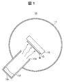
- FIG. 1 is a cross-sectional view schematically showing a configuration of a film forming apparatus for manufacturing an organic semiconductor film according to the present embodiment.
- an ultra-high vacuum film forming apparatus 10 includes a chamber 11 and a raw material cell 12 attached to the chamber 11.
- a stage 13 on which a substrate G made of, for example, a silicon substrate, a glass substrate, or a plastic (polymer) substrate can be mounted is disposed in the chamber 11, and the stage 13 is mounted with a heater (not shown). The substrate G is heated.
- the chamber 11 has an exhaust device (not shown), and the exhaust device exhausts the inside of the chamber 11 to reduce the pressure.
- the raw material cell 12 has a cylindrical main body with one open end, and is attached to the chamber 11 so that the open end 12a faces the stage 13, and contains an organic compound (for example, CHP) powder inside. To accommodate.
- the raw material cell 12 has a heater (not shown) in the vicinity of the open end 12b, and the heater heats and sublimates the organic compound contained in the main body.
- the sublimated organic compound enters the chamber 11 and is deposited on the surface of the catalytic metal layer M formed on the surface of the substrate G.
- the catalytic metal layer M is a single crystal metal having catalytic ability, for example, a transition metal having a face-centered cubic lattice (Cu, Ni, Au, etc.), a transition metal having a hexagonal close-packed structure (Co, Ru, etc.), or these
- the single crystal metal is a transition metal having a face-centered cubic lattice
- the surface of the catalytic metal layer M is composed of the (111) plane that is the closest crystal plane in the face-centered cubic lattice.
- the surface of the catalyst metal layer M is composed of the (0001) plane that is the close-packed crystal plane in the hexagonal close-packed structure.
- the plurality of CHP molecules to which thermal energy is applied in the raw material cell 12 collide with the catalytic metal layer M, and bromine is desorbed from the CHP molecules due to the energy of each molecule and the catalytic action of the catalytic metal layer M, and a plurality of phenyl molecules. Radicals are generated. Each phenyl radical is polymerized with each other by the catalytic action of the catalytic metal layer M, the heating from the heater of the stage 13 and the Ullmann reaction caused by the energy of each molecule. At this time, each phenyl radical is polymerized based on the spontaneous ordering of the CHP molecules, thereby forming a first two-dimensional network structure. In the present embodiment, collision of CHP molecules with the catalyst metal layer M and desorption of bromine from CHP molecules are performed in the gas phase.
- the honeycomb structure of the phenyl group is a close-packed crystal plane constituting the surface of the catalyst metal layer M (for example, the (111) plane when the catalyst metal layer M is made of a transition metal having a face-centered cubic lattice,
- the metal layer M is made of a transition metal having a hexagonal close-packed structure, it is easy to lattice match with the (0001) plane. Therefore, the polymerization of the phenyl radical proceeds along the surface of the catalytic metal layer M. Therefore, the first two-dimensional network structure formed on the surface of the catalytic metal layer M is a single layer.
- the catalytic metal layer M is not a single crystal metal but has a catalytic ability and is a polycrystalline metal containing grains, such as a transition metal (Cu, Ni, Au, etc.) having a face-centered cubic lattice or hexagonal.
- a transition metal Cu, Ni, Au, etc.
- the polycrystalline metal is a transition metal having a face-centered cubic lattice
- the surface of the grain is a face-centered cubic lattice.
- the polycrystalline metal is a transition metal having a hexagonal close-packed structure
- the grain surface is the close-packed crystal plane in the hexagonal close-packed structure (0001). ) Surface.
- CHP having iodine as a halogen in the side chain instead of CHP having bromine in the side chain.
- iodine has a vapor pressure lower than that of bromine, iodine released when forming the first two-dimensional network structure may be bonded to each other, and may remain on the surface of the catalytic metal layer M as a solid. It is not preferable to use CHP having iodine in obtaining a pseudo graphene structure constituted by one two-dimensional network structure.
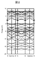
- the inventor calculated the band gap of the pseudo graphene structure constituted by the first two-dimensional network structure by the first principle calculation based on the density functional method. As shown in FIG. In FIG. 5, it was confirmed that the lower end of the conduction band (indicated by a solid circle in the drawing) and the upper end of the valence band (indicated by a broken circle in the drawing) were separated to generate a band gap.
- the band gap in the band diagram of FIG. 2 was 2.27 eV. That is, it has been found that an organic semiconductor film having a pseudo graphene structure constituted by the first two-dimensional network structure exhibits semiconductor characteristics necessary for realizing a switching operation.
- the present inventor calculated the energy required for desorption of bromine from the organic compound by quantum chemical calculation. Specifically, the energy required for elimination of bromine (Br 2 ) from bromobenzene (C 6 H 5 Br) or tetra (4-bromophenyl) porphyrin (Br 4 TPP) as an organic compound, and desorption of bromine radicals. When the separation energy was calculated, it was calculated that these energies were about 3 eV or more. In other words, desorption of bromine and bromine radicals from organic compounds requires a large amount of energy, and it is difficult to desorb bromine and the like only by heating the organic compound. It was found that the application of light energy by light irradiation is necessary.
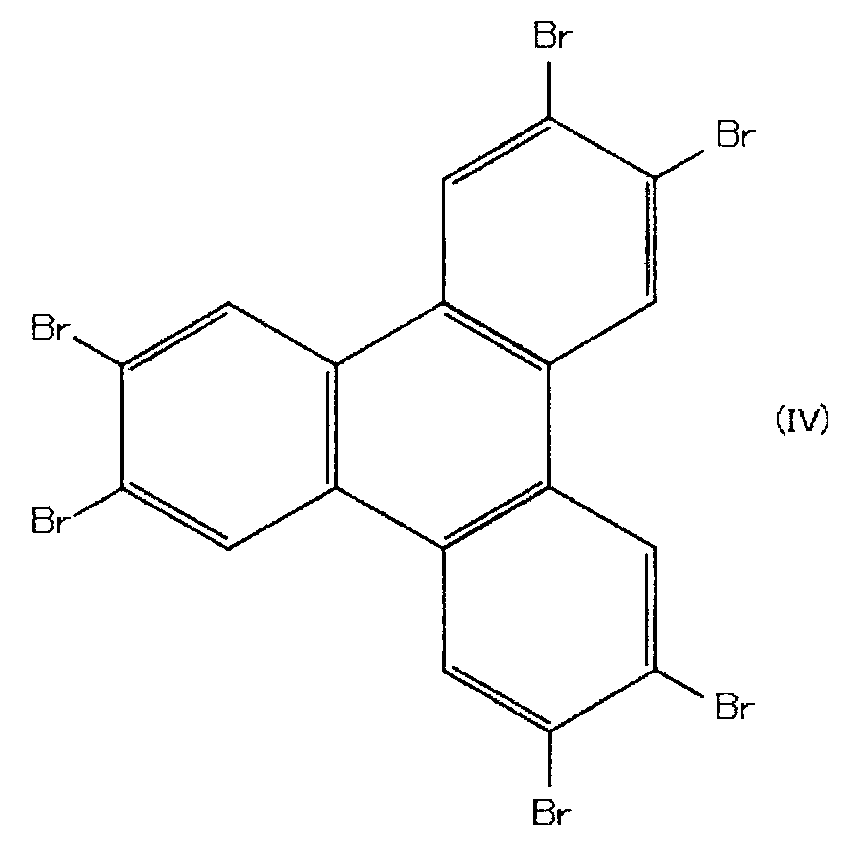
- the organic semiconductor film according to the present embodiment is manufactured from HBTP which is a molecule of an organic compound represented by the following formula (IV).
- HBTP represented by the above formula (IV) has bromine as a halogen in the side chain.
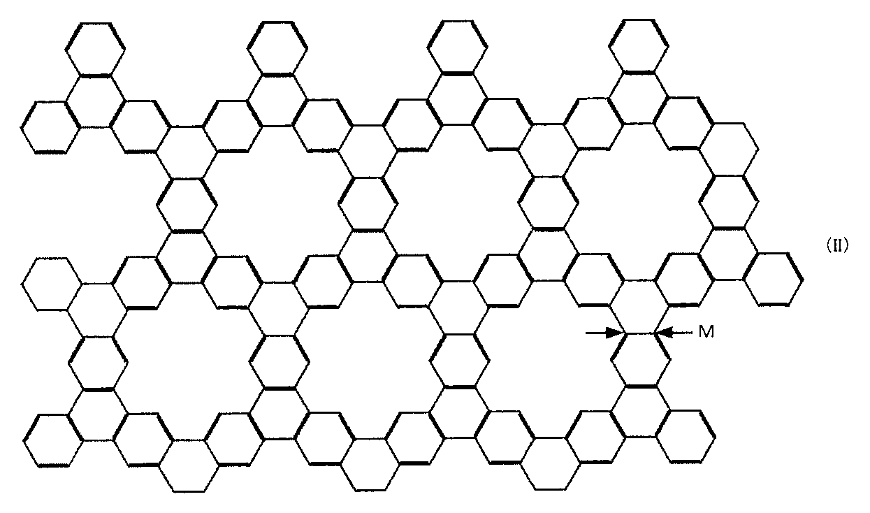
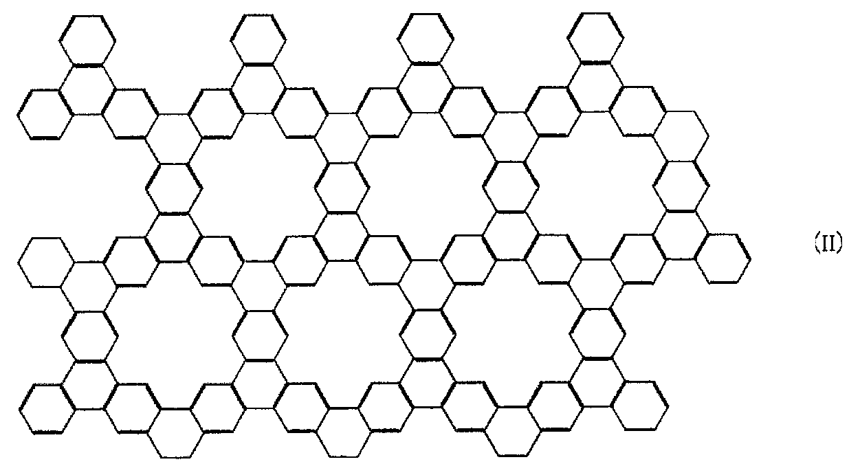
- the HBTP is represented by the following formula (II) from a plurality of HBTPs represented by the above formula (IV). A two-dimensional network structure is formed.
- the two-dimensional network structure represented by the above formula (II) (hereinafter referred to as “second two-dimensional network structure”) is formed to form a pseudo graphene structure.
- the neck in the second two-dimensional network structure is a portion between two adjacent phenyl groups (indicated by “M” in the above formula (II)), the width of the neck is ⁇ order, It is about 1.42 mm which is equal to the bond distance between carbon atoms.
- the neck in the second two-dimensional network structure is uniquely determined according to the shape and modification group of HBTP. That is, when an organic semiconductor film is manufactured by forming a second two-dimensional network structure from a plurality of HBTPs and obtaining a pseudo-graphene structure, a neck with a width of ⁇ order can always be formed. A desired band gap can be reliably obtained by the size effect.
- the ultra-high vacuum film forming apparatus 10 of FIG. 1 is used.
- bromine is desorbed by the catalytic action of the catalytic metal layer M and the like.
- the generated phenyl radicals are polymerized by the Ullmann reaction, and when each phenyl radical is polymerized, the elimination of bromine and the Ullmann reaction are interfacial reactions, so they occur only in the HBTP molecules that are in direct contact with the catalytic metal layer M.
- the honeycomb structure of the phenyl group of each phenyl radical has a close-packed crystal plane constituting the surface of the catalytic metal layer M (for example, a transition metal in which the catalytic metal layer M has a face-centered cubic lattice). (111) plane, and (0001) plane when the catalyst metal layer M is made of a transition metal having a hexagonal close-packed structure).
- Polymerization of Rurajikaru proceeds along the surface of the catalyst metal layer M. Therefore, the second two-dimensional network structure formed on the surface of the catalytic metal layer M is a single layer.
- the catalytic metal layer M is not a single crystal metal, has a catalytic ability, and has a grain-containing polycrystalline metal, for example, a transition having a face-centered cubic lattice. It is composed of a metal (Cu, Ni, Au, etc.), a transition metal (Co, Ru, etc.) having a hexagonal close-packed structure, or an alloy containing these transition metals, and a polycrystalline metal is a transition metal having a face-centered cubic lattice.
- the grain surface is composed of the (111) plane which is the closest packed crystal face in the face-centered cubic lattice, and the polycrystalline metal is a transition metal having a hexagonal close packed structure
- the grain surface is hexagonal close packed.
- You may comprise by the (0001) plane which is the closest crystal plane in a structure.
- the polymerization of the phenyl radical proceeds along the surface of the grain, forming a single-layer second two-dimensional network structure.
- the inventor calculated the band gap of the pseudo graphene structure constituted by the second two-dimensional network structure by the first principle calculation based on the density functional method, as in the first embodiment.
- the lower end of the conduction band shown by a solid circle in the drawing
- the upper end of the valence band shown by a broken circle in the drawing
- the band gap in the band diagram of FIG. 3 was 1.77 eV. That is, it was found that the organic semiconductor film having a pseudo graphene structure constituted by the second two-dimensional network structure also exhibits semiconductor characteristics necessary for realizing the switching operation.
- FIG. 4 is a cross-sectional view schematically showing a configuration of an example of a bottom-gate thin film transistor structure to which the organic semiconductor film according to each embodiment is applied.
- the thin film transistor structure 14 is formed on a gate electrode 15 formed on a substrate (not shown), a gate insulating film 16 formed on the gate electrode 15, and the gate insulating film 16.
- a channel layer 17 and a source electrode 18 and a drain electrode 19 formed on the channel layer 17 are provided.
- the channel layer 17 is the organic semiconductor film according to the first embodiment or the second embodiment. It consists of an organic semiconductor film.
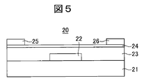
- FIG. 5 is a cross-sectional view schematically showing a configuration of a first modified example of a bottom-gate thin film transistor structure to which the organic semiconductor film according to each embodiment is applied.
- the thin film transistor structure 20 is formed on the gate electrode 22 formed on the substrate 21, the gate insulating film 23 formed so as to cover the substrate 21 and the gate electrode 22, and the gate insulating film 23.
- the channel layer 24 includes a source electrode 25 and a drain electrode 26 formed on the channel layer 24.
- the channel layer 24 is the organic semiconductor film according to the first embodiment or the second embodiment. It consists of an organic semiconductor film.
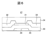
- FIG. 6 is a cross-sectional view schematically showing a configuration of a second modification of the bottom gate type thin film transistor structure to which the organic semiconductor film according to each embodiment is applied.
- a thin film transistor structure 27 includes an undercoat layer 28 formed on a substrate (not shown), a gate electrode 29 partially formed on the undercoat layer 28, an undercoat layer 28, and A gate insulating film 30 formed so as to cover the gate electrode 29, a channel layer 31 formed on the gate insulating film 30 so as to be disposed immediately above the gate electrode 29, and on the gate insulating film 30 A source electrode 32 and a drain electrode 33 formed on both sides of the channel layer 31; and a passivation layer 34 formed so as to cover the channel layer 31, the source electrode 32, and the drain electrode 33.
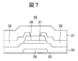
- FIG. 7 is a cross-sectional view schematically showing a configuration of a third modification of the bottom-gate thin film transistor structure to which the organic semiconductor film according to each embodiment is applied.
- the thin film transistor structure 35 includes an undercoat layer 28 formed on a substrate (not shown), a gate electrode 29 partially formed on the undercoat layer 28, an undercoat layer 28, and A gate insulating film 30 formed so as to cover the gate electrode 29, a channel layer 31 formed on the gate insulating film 30 so as to be disposed immediately above the gate electrode 29, and on the gate insulating film 30
- the source electrode 32 and the drain electrode 33 formed on both sides of the channel layer 31, the etching stopper layer 36 formed so as to cover the channel layer 31, and the etching stopper layer 36, the source electrode 32, and the drain electrode 33 are covered.
- the channel layer 31 is formed according to the first embodiment.
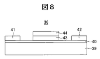
- FIG. 8 is a cross-sectional view schematically showing a configuration of an example of a top gate type thin film transistor structure to which the organic semiconductor film according to each embodiment is applied.
- a thin film transistor structure 38 includes a channel layer 40 formed on a substrate 39, a source electrode 41 and a drain electrode 42 formed on the channel layer 40 so as to be separated from each other, and a source on the channel layer 40.
- the gate insulating film 43 formed between the electrode 41 and the drain electrode 42 and the gate electrode 44 formed on the gate insulating film 43 are provided, and the channel layer 40 is the organic semiconductor according to the first embodiment. It consists of a film or the organic semiconductor film according to the second embodiment. Note that a passivation layer may be interposed between the substrate 39 and the channel layer 40.
- FIG. 9 is a cross-sectional view schematically showing a configuration of a first modification of a top gate type thin film transistor structure to which the organic semiconductor film according to each embodiment is applied.
- the thin film transistor structure 45 includes an undercoat layer 46 formed on a substrate (not shown), a channel layer 47 partially formed on the undercoat layer 46, and the undercoat layer 46. , A source electrode 48 and a drain electrode 49 formed on both sides of the channel layer 47, a gate insulating film 50 formed so as to cover the channel layer 47, the source electrode 48, and the drain electrode 49, and the gate insulating film 50, respectively. And a passivation layer 52 formed so as to cover the gate electrode 51 and the gate insulating film 50.
- the channel layer 47 includes The organic semiconductor film according to the first embodiment or the organic semiconductor film according to the second embodiment.
- FIG. 10 is a cross-sectional view schematically showing a configuration of a second modification of the top gate type thin film transistor structure to which the organic semiconductor film according to each embodiment is applied.
- a thin film transistor structure 53 is connected to an undercoat layer 46 formed on a substrate (not shown), a channel layer 47 partially formed on the undercoat layer 46, and the channel layer 47.
- the channel layer 47 is formed of the organic semiconductor film according to the first embodiment or the second layer. It made of an organic semiconductor film according to the facilities of the form.
- the channel layers 17, 24, 31, 40, and 47 can be formed as thin films having a thickness of several tens of meters. Since a band gap is generated in these organic semiconductor films, the thin film transistor structures 14, 20, 27, 35, 38, 45, and 53 can perform a switching operation.
- the substrates 21 and 39 are flexible members, such as glass thin plates, metal thin plates (for example, stainless steel), or resin substrates (for example, polycarbonate, polyethylene terephthalate). , Polyethylene naphthalate, cyclic olefin polymer (ATRON, APEL, ZEONEX), polyarylate, aromatic polyether ketone, aromatic polyether sulfone, wholly aromatic polyketone or polyimide).
- the gate insulating films 16, 23, 30, 43, and 50 are made of polymer materials (for example, polychloropyrene, polyethylene terephthalate, polyoxymethylene, polyvinyl chloride, polyvinylidene fluoride, cyanoethyl pullulan, polymethyl methacrylate, polysulfone, polycarbonate, polyvinyl). Phenol, polystyrene or polyimide) or an inorganic material (for example, SiO 2 , SiN, Al 2 O 3 , HfO 2 or BN) is preferable.
- polymer materials for example, polychloropyrene, polyethylene terephthalate, polyoxymethylene, polyvinyl chloride, polyvinylidene fluoride, cyanoethyl pullulan, polymethyl methacrylate, polysulfone, polycarbonate, polyvinyl.
- Phenol, polystyrene or polyimide or an inorganic material (for example, SiO
- the gate electrodes 15, 22, 29, 44, 51, the source electrodes 18, 25, 32, 41, 48 and the drain electrodes 19, 26, 33, 42, 49 are made of metal (eg, Ag, Al, Cu, Pt). , Au, Ni, Co, Pd, Ti and Cr), an oxide conductor (for example, ITO (indium tin oxide) and ZnO (zinc oxide)), or an organic material-based conductor (for example, a conductive polymer). Is preferred.
- the organic semiconductor film according to each embodiment is manufactured using the ultra-high vacuum film forming apparatus 10 of FIG. 1, but the organic semiconductor film according to each embodiment is formed using a conventional vapor deposition film forming apparatus (for example, a low deposition film forming apparatus). You may manufacture with a vacuum film-forming apparatus and a resistance heating type film-forming apparatus.
- a conventional vapor deposition film forming apparatus for example, a low deposition film forming apparatus.
Landscapes
- Chemical & Material Sciences (AREA)
- Organic Chemistry (AREA)
- Engineering & Computer Science (AREA)
- Physics & Mathematics (AREA)
- Materials Engineering (AREA)
- Spectroscopy & Molecular Physics (AREA)
- Polymers & Plastics (AREA)
- Health & Medical Sciences (AREA)
- Medicinal Chemistry (AREA)
- Chemical Kinetics & Catalysis (AREA)
- Manufacturing & Machinery (AREA)
- Crystallography & Structural Chemistry (AREA)
- Thin Film Transistor (AREA)
- Organic Low-Molecular-Weight Compounds And Preparation Thereof (AREA)
- Low-Molecular Organic Synthesis Reactions Using Catalysts (AREA)
- Polyoxymethylene Polymers And Polymers With Carbon-To-Carbon Bonds (AREA)
- Electroluminescent Light Sources (AREA)
Abstract
Description

17 チャネル層
Claims (19)
- 下記式(I)
- 前記疑似グラフェン構造は前記二次元ネットワーク構造の単層からなることを特徴とする請求項1記載の有機半導体膜。
- 下記式(II)
- 前記疑似グラフェン構造は前記二次元ネットワーク構造の単層からなることを特徴とする請求項3記載の有機半導体膜。
- 前記請求項1又は2記載の有機半導体膜における前記二次元ネットワーク構造が、複数の5,5’,5’’,5’’’,5’’’’,5’’’’’−ヘキサブロモシクロヘキサ−m−フェニレン(CHP)を互いに重合反応させて形成され、前記CHPは側鎖に臭素を有することを特徴とする有機半導体膜の製造方法。
- 前記二次元ネットワーク構造は、前記複数のCHPを、触媒能を有する単結晶金属の表面に蒸着させることによって形成されることを特徴とする請求項5記載の有機半導体膜の製造方法。
- 前記単結晶金属が面心立方格子を有する場合、前記単結晶金属の表面を前記面心立方格子における(111)面で構成することを特徴とする請求項6記載の有機半導体膜の製造方法。
- 前記単結晶金属が六方最密構造を有する場合、前記単結晶金属の表面を前記六方最密構造における(0001)面で構成することを特徴とする請求項6記載の有機半導体膜の製造方法。
- 前記二次元ネットワーク構造は、前記複数のCHPを、触媒能を有するグレインを含む多結晶金属の表面に蒸着させることによって形成されることを特徴とする請求項5記載の有機半導体膜の製造方法。
- 前記多結晶金属が面心立方格子を有する場合、前記グレインの表面を前記面心立方格子における(111)面で構成することを特徴とする請求項9記載の有機半導体膜の製造方法。
- 前記多結晶金属が六方最密構造を有する場合、前記グレインの表面を前記六方最密構造における(0001)面で構成することを特徴とする請求項9記載の有機半導体膜の製造方法。
- 前記請求項3又は4記載の有機半導体膜における前記二次元ネットワーク構造が、複数の2,3,6,7,10,11−ヘキサブロモトリフェニレン(HBTP)を互いに重合反応させて形成されることを特徴とする有機半導体膜の製造方法。
- 前記二次元ネットワーク構造は、前記複数のHBTPを、触媒能を有する単結晶金属の表面に蒸着させることによって形成されることを特徴とする請求項12記載の有機半導体膜の製造方法。
- 前記単結晶金属が面心立方格子を有する場合、前記単結晶金属の表面を前記面心立方格子における(111)面で構成することを特徴とする請求項13記載の有機半導体膜の製造方法。
- 前記単結晶金属が六方最密構造を有する場合、前記単結晶金属の表面を前記六方最密構造における(0001)面で構成することを特徴とする請求項13記載の有機半導体膜の製造方法。
- 前記二次元ネットワーク構造は、前記複数のHBTPを、触媒能を有するグレインを含む多結晶金属の表面に蒸着させることによって形成されることを特徴とする請求項12記載の有機半導体膜の製造方法。
- 前記多結晶金属が面心立方格子を有する場合、前記グレインの表面を前記面心立方格子における(111)面で構成することを特徴とする請求項16記載の有機半導体膜の製造方法。
- 前記多結晶金属が六方最密構造を有する場合、前記グレインの表面を前記六方最密構造における(0001)面で構成することを特徴とする請求項16記載の有機半導体膜の製造方法。
- 請求項1乃至4のいずれか1項に記載の有機半導体膜をチャネルに用いることを特徴とするトランジスタ構造。
Priority Applications (2)
| Application Number | Priority Date | Filing Date | Title |
|---|---|---|---|
| KR1020157033841A KR102182527B1 (ko) | 2013-06-03 | 2014-05-27 | 유기 반도체막, 그 제조 방법 및 트랜지스터 구조 |
| US14/895,404 US20160118589A1 (en) | 2013-06-03 | 2014-05-27 | Organic Semiconductor Film, Method for Manufacturing Same, and Transistor Structure |
Applications Claiming Priority (2)
| Application Number | Priority Date | Filing Date | Title |
|---|---|---|---|
| JP2013-116758 | 2013-06-03 | ||
| JP2013116758A JP6062321B2 (ja) | 2013-06-03 | 2013-06-03 | 有機半導体膜、その製造方法及びトランジスタ構造 |
Publications (1)
| Publication Number | Publication Date |
|---|---|
| WO2014196487A1 true WO2014196487A1 (ja) | 2014-12-11 |
Family
ID=52008129
Family Applications (1)
| Application Number | Title | Priority Date | Filing Date |
|---|---|---|---|
| PCT/JP2014/064563 Ceased WO2014196487A1 (ja) | 2013-06-03 | 2014-05-27 | 有機半導体膜、その製造方法及びトランジスタ構造 |
Country Status (4)
| Country | Link |
|---|---|
| US (1) | US20160118589A1 (ja) |
| JP (1) | JP6062321B2 (ja) |
| KR (1) | KR102182527B1 (ja) |
| WO (1) | WO2014196487A1 (ja) |
Families Citing this family (3)
| Publication number | Priority date | Publication date | Assignee | Title |
|---|---|---|---|---|
| JP6657596B2 (ja) * | 2014-11-11 | 2020-03-04 | コニカミノルタ株式会社 | 有機エレクトロニクス素子 |
| JP6839355B2 (ja) | 2017-02-08 | 2021-03-10 | 富士通株式会社 | グラフェンナノリボン、グラフェンナノリボンの製造方法及び半導体装置 |
| CN118878850B (zh) * | 2024-08-16 | 2025-03-21 | 同济大学 | 一种卟啉基二维石墨炔非线性光学薄膜材料及其制备和应用 |
Citations (4)
| Publication number | Priority date | Publication date | Assignee | Title |
|---|---|---|---|---|
| JP2003516422A (ja) * | 1999-12-08 | 2003-05-13 | ユニヴァーシティ・オヴ・リーズ | 導電性液晶の新しいファミリー |
| JP2007242712A (ja) * | 2006-03-06 | 2007-09-20 | Toyota Central Res & Dev Lab Inc | 有機電界発光素子 |
| WO2011111719A1 (ja) * | 2010-03-08 | 2011-09-15 | 国立大学法人名古屋大学 | カーボンナノリング及びその製造原料として好適な輪状の化合物の製造方法 |
| JP2013071208A (ja) * | 2011-09-28 | 2013-04-22 | Denso Wave Inc | ロボット |
Family Cites Families (4)
| Publication number | Priority date | Publication date | Assignee | Title |
|---|---|---|---|---|
| BRPI0507173A (pt) * | 2004-01-28 | 2007-06-26 | Solvay Advanced Polymers Llc | método para produzir polìmeros de polifenileno substituìdo |
| KR101443222B1 (ko) * | 2007-09-18 | 2014-09-19 | 삼성전자주식회사 | 그라펜 패턴 및 그의 형성방법 |
| JP2010212619A (ja) | 2009-03-12 | 2010-09-24 | Toshiba Corp | グラフェンの作製方法、グラフェン、グラフェン作製装置及び半導体素子 |
| JP5794075B2 (ja) * | 2011-09-28 | 2015-10-14 | 富士通株式会社 | 電子装置およびその製造方法 |
-
2013
- 2013-06-03 JP JP2013116758A patent/JP6062321B2/ja not_active Expired - Fee Related
-
2014
- 2014-05-27 KR KR1020157033841A patent/KR102182527B1/ko active Active
- 2014-05-27 WO PCT/JP2014/064563 patent/WO2014196487A1/ja not_active Ceased
- 2014-05-27 US US14/895,404 patent/US20160118589A1/en not_active Abandoned
Patent Citations (4)
| Publication number | Priority date | Publication date | Assignee | Title |
|---|---|---|---|---|
| JP2003516422A (ja) * | 1999-12-08 | 2003-05-13 | ユニヴァーシティ・オヴ・リーズ | 導電性液晶の新しいファミリー |
| JP2007242712A (ja) * | 2006-03-06 | 2007-09-20 | Toyota Central Res & Dev Lab Inc | 有機電界発光素子 |
| WO2011111719A1 (ja) * | 2010-03-08 | 2011-09-15 | 国立大学法人名古屋大学 | カーボンナノリング及びその製造原料として好適な輪状の化合物の製造方法 |
| JP2013071208A (ja) * | 2011-09-28 | 2013-04-22 | Denso Wave Inc | ロボット |
Non-Patent Citations (2)
| Title |
|---|
| BALAZS H. ET AL: "NOVEL SERIES OF GIANT POLYCYCLIC AROMATIC HYDROCARBONS ELECTRONIC STRUCTURE AND AROMATICITY", CHEMICAL PHYSICS LETTERS, vol. 385, 2004, pages 512 - 518 * |
| BIERI M. ET AL: "TWO DIMENSIONAL POLYMER FORMATION ON SURFACES INSIGHT INTO THE ROLES OF PRECURSOR MOBILITY AND REACTIVITY", JOURNAL OF THE AMERICAN CHEMICAL SOCIETY, 2 November 2010 (2010-11-02), pages 16669 - 16676 * |
Also Published As
| Publication number | Publication date |
|---|---|
| US20160118589A1 (en) | 2016-04-28 |
| KR20160016804A (ko) | 2016-02-15 |
| JP6062321B2 (ja) | 2017-01-18 |
| KR102182527B1 (ko) | 2020-11-24 |
| JP2014236111A (ja) | 2014-12-15 |
Similar Documents
| Publication | Publication Date | Title |
|---|---|---|
| Kim et al. | Atomic layer etching mechanism of MoS2 for nanodevices | |
| Roth et al. | Chemical vapor deposition and characterization of aligned and incommensurate graphene/hexagonal boron nitride heterostack on Cu (111) | |
| Basagni et al. | Molecules–oligomers–nanowires–graphene nanoribbons: a bottom-up stepwise on-surface covalent synthesis preserving long-range order | |
| Ismach et al. | Toward the controlled synthesis of hexagonal boron nitride films | |
| Wang et al. | Primary nucleation-dominated chemical vapor deposition growth for uniform graphene monolayers on dielectric substrate | |
| Jang et al. | Wafer-scale and wrinkle-free epitaxial growth of single-orientated multilayer hexagonal boron nitride on sapphire | |
| Rasool et al. | Continuity of graphene on polycrystalline copper | |
| Wang et al. | Selective direct growth of atomic layered HfS2 on hexagonal boron nitride for high performance photodetectors | |
| Nie et al. | Growth from below: graphene bilayers on Ir (111) | |
| Kidambi et al. | In situ observations during chemical vapor deposition of hexagonal boron nitride on polycrystalline copper | |
| Dumcenco et al. | Large-area epitaxial monolayer MoS2 | |
| Kim et al. | Synthesis and characterization of hexagonal boron nitride film as a dielectric layer for graphene devices | |
| Qiu et al. | From silicene to half-silicane by hydrogenation | |
| Kidambi et al. | Observing graphene grow: catalyst–graphene interactions during scalable graphene growth on polycrystalline copper | |
| Liu et al. | Controllable and rapid synthesis of high-quality and large-area Bernal stacked bilayer graphene using chemical vapor deposition | |
| Sutter et al. | Chemical vapor deposition and etching of high-quality monolayer hexagonal boron nitride films | |
| Liu et al. | Direct growth of graphene/hexagonal boron nitride stacked layers | |
| Bhaumik et al. | Conversion of p to n-type reduced graphene oxide by laser annealing at room temperature and pressure | |
| US8946692B2 (en) | Graphene (multilayer) boron nitride heteroepitaxy for electronic device applications | |
| Massimi et al. | Surface-assisted reactions toward formation of graphene nanoribbons on Au (110) surface | |
| Wu et al. | Bilayer graphene growth via a penetration mechanism | |
| Hayashi et al. | Selective graphene formation on copper twin crystals | |
| JP6004092B2 (ja) | 積層体および積層体の製造方法 | |
| Song et al. | Graphene/h‐BN heterostructures: recent advances in controllable preparation and functional applications | |
| CN103031516B (zh) | 一种六角相氮化硼薄膜的制备方法 |
Legal Events
| Date | Code | Title | Description |
|---|---|---|---|
| 121 | Ep: the epo has been informed by wipo that ep was designated in this application |
Ref document number: 14807929 Country of ref document: EP Kind code of ref document: A1 |
|
| ENP | Entry into the national phase |
Ref document number: 20157033841 Country of ref document: KR Kind code of ref document: A |
|
| WWE | Wipo information: entry into national phase |
Ref document number: 14895404 Country of ref document: US |
|
| NENP | Non-entry into the national phase |
Ref country code: DE |
|
| 122 | Ep: pct application non-entry in european phase |
Ref document number: 14807929 Country of ref document: EP Kind code of ref document: A1 |