WO2014189122A1 - 化合物、発光材料および有機発光素子 - Google Patents
化合物、発光材料および有機発光素子 Download PDFInfo
- Publication number
- WO2014189122A1 WO2014189122A1 PCT/JP2014/063638 JP2014063638W WO2014189122A1 WO 2014189122 A1 WO2014189122 A1 WO 2014189122A1 JP 2014063638 W JP2014063638 W JP 2014063638W WO 2014189122 A1 WO2014189122 A1 WO 2014189122A1
- Authority
- WO
- WIPO (PCT)
- Prior art keywords
- group
- substituted
- carbon atoms
- general formula
- substituent
- Prior art date
Links
- 150000001875 compounds Chemical class 0.000 title claims abstract description 111
- 239000000463 material Substances 0.000 title claims abstract description 94
- 125000004432 carbon atom Chemical group C* 0.000 claims description 108
- 125000001424 substituent group Chemical group 0.000 claims description 64
- 125000004435 hydrogen atom Chemical group [H]* 0.000 claims description 48
- 238000005401 electroluminescence Methods 0.000 claims description 43
- 230000003111 delayed effect Effects 0.000 claims description 33
- 125000003118 aryl group Chemical group 0.000 claims description 23
- HEDRZPFGACZZDS-UHFFFAOYSA-N Chloroform Chemical compound ClC(Cl)Cl HEDRZPFGACZZDS-UHFFFAOYSA-N 0.000 claims description 22
- 125000004093 cyano group Chemical group *C#N 0.000 claims description 21
- 125000003545 alkoxy group Chemical group 0.000 claims description 19
- 125000000217 alkyl group Chemical group 0.000 claims description 19
- 125000001072 heteroaryl group Chemical group 0.000 claims description 18
- 125000004122 cyclic group Chemical group 0.000 claims description 15
- 239000000758 substrate Substances 0.000 claims description 15
- 229910052801 chlorine Inorganic materials 0.000 claims description 10
- 125000001309 chloro group Chemical group Cl* 0.000 claims description 10
- 238000000034 method Methods 0.000 claims description 10
- 229910052731 fluorine Inorganic materials 0.000 claims description 9
- 125000001153 fluoro group Chemical group F* 0.000 claims description 9
- 229910052799 carbon Inorganic materials 0.000 claims description 8
- 125000004663 dialkyl amino group Chemical group 0.000 claims description 8
- 125000004986 diarylamino group Chemical group 0.000 claims description 8
- 125000001997 phenyl group Chemical group [H]C1=C([H])C([H])=C(*)C([H])=C1[H] 0.000 claims description 8
- OKTJSMMVPCPJKN-UHFFFAOYSA-N Carbon Chemical compound [C] OKTJSMMVPCPJKN-UHFFFAOYSA-N 0.000 claims description 6
- OAICVXFJPJFONN-UHFFFAOYSA-N Phosphorus Chemical compound [P] OAICVXFJPJFONN-UHFFFAOYSA-N 0.000 claims description 5
- 150000001721 carbon Chemical group 0.000 claims description 2
- 239000010410 layer Substances 0.000 description 150
- YXFVVABEGXRONW-UHFFFAOYSA-N Toluene Chemical compound CC1=CC=CC=C1 YXFVVABEGXRONW-UHFFFAOYSA-N 0.000 description 48
- 230000000903 blocking effect Effects 0.000 description 40
- IJGRMHOSHXDMSA-UHFFFAOYSA-N Atomic nitrogen Chemical compound N#N IJGRMHOSHXDMSA-UHFFFAOYSA-N 0.000 description 36
- 238000002347 injection Methods 0.000 description 22
- 239000007924 injection Substances 0.000 description 22
- 239000000203 mixture Substances 0.000 description 21
- 229910052757 nitrogen Inorganic materials 0.000 description 21
- 238000005424 photoluminescence Methods 0.000 description 21
- 230000005525 hole transport Effects 0.000 description 17
- 229940125904 compound 1 Drugs 0.000 description 16
- 238000003786 synthesis reaction Methods 0.000 description 16
- 230000015572 biosynthetic process Effects 0.000 description 15
- 229940125782 compound 2 Drugs 0.000 description 12
- VLKZOEOYAKHREP-UHFFFAOYSA-N n-Hexane Chemical compound CCCCCC VLKZOEOYAKHREP-UHFFFAOYSA-N 0.000 description 12
- 239000012044 organic layer Substances 0.000 description 12
- 229920000642 polymer Polymers 0.000 description 12
- BWHMMNNQKKPAPP-UHFFFAOYSA-L potassium carbonate Chemical compound [K+].[K+].[O-]C([O-])=O BWHMMNNQKKPAPP-UHFFFAOYSA-L 0.000 description 10
- BWHDROKFUHTORW-UHFFFAOYSA-N tritert-butylphosphane Chemical compound CC(C)(C)P(C(C)(C)C)C(C)(C)C BWHDROKFUHTORW-UHFFFAOYSA-N 0.000 description 10
- 238000006243 chemical reaction Methods 0.000 description 9
- 239000010409 thin film Substances 0.000 description 9
- FYYHWMGAXLPEAU-UHFFFAOYSA-N Magnesium Chemical compound [Mg] FYYHWMGAXLPEAU-UHFFFAOYSA-N 0.000 description 8
- 229910052782 aluminium Inorganic materials 0.000 description 8
- XAGFODPZIPBFFR-UHFFFAOYSA-N aluminium Chemical compound [Al] XAGFODPZIPBFFR-UHFFFAOYSA-N 0.000 description 8
- 239000011777 magnesium Substances 0.000 description 8
- 229910052749 magnesium Inorganic materials 0.000 description 8
- 238000005259 measurement Methods 0.000 description 8
- 239000007787 solid Substances 0.000 description 8
- 230000001052 transient effect Effects 0.000 description 8
- 239000007772 electrode material Substances 0.000 description 7
- 238000000295 emission spectrum Methods 0.000 description 7
- 230000005284 excitation Effects 0.000 description 7
- 238000004020 luminiscence type Methods 0.000 description 7
- 229910052751 metal Inorganic materials 0.000 description 7
- 239000002184 metal Substances 0.000 description 7
- 239000000243 solution Substances 0.000 description 7
- 125000005843 halogen group Chemical group 0.000 description 6
- -1 isopropyloxy group Chemical group 0.000 description 6
- 125000005647 linker group Chemical group 0.000 description 6
- 125000001791 phenazinyl group Chemical group C1(=CC=CC2=NC3=CC=CC=C3N=C12)* 0.000 description 6
- 238000001296 phosphorescence spectrum Methods 0.000 description 6
- IVURTNNWJAPOML-UHFFFAOYSA-N 5,10-dihydrophenazine Chemical compound C1=CC=C2NC3=CC=CC=C3NC2=C1 IVURTNNWJAPOML-UHFFFAOYSA-N 0.000 description 5
- 0 Cc(cccc1)c1-c1nc(CC=CC=CC#*)nc(C)n1 Chemical compound Cc(cccc1)c1-c1nc(CC=CC=CC#*)nc(C)n1 0.000 description 5
- CSNNHWWHGAXBCP-UHFFFAOYSA-L Magnesium sulfate Chemical compound [Mg+2].[O-][S+2]([O-])([O-])[O-] CSNNHWWHGAXBCP-UHFFFAOYSA-L 0.000 description 5
- 239000012267 brine Substances 0.000 description 5
- 230000005587 bubbling Effects 0.000 description 5
- 238000001816 cooling Methods 0.000 description 5
- 230000018044 dehydration Effects 0.000 description 5
- 238000006297 dehydration reaction Methods 0.000 description 5
- 239000010408 film Substances 0.000 description 5
- 239000011259 mixed solution Substances 0.000 description 5
- 239000000178 monomer Substances 0.000 description 5
- LXNAVEXFUKBNMK-UHFFFAOYSA-N palladium(II) acetate Substances [Pd].CC(O)=O.CC(O)=O LXNAVEXFUKBNMK-UHFFFAOYSA-N 0.000 description 5
- YJVFFLUZDVXJQI-UHFFFAOYSA-L palladium(ii) acetate Chemical compound [Pd+2].CC([O-])=O.CC([O-])=O YJVFFLUZDVXJQI-UHFFFAOYSA-L 0.000 description 5
- 229910000027 potassium carbonate Inorganic materials 0.000 description 5
- HPALAKNZSZLMCH-UHFFFAOYSA-M sodium;chloride;hydrate Chemical compound O.[Na+].[Cl-] HPALAKNZSZLMCH-UHFFFAOYSA-M 0.000 description 5
- 239000002904 solvent Substances 0.000 description 5
- 238000007740 vapor deposition Methods 0.000 description 5
- 229940125898 compound 5 Drugs 0.000 description 4
- 238000000921 elemental analysis Methods 0.000 description 4
- 238000011156 evaluation Methods 0.000 description 4
- 125000005842 heteroatom Chemical group 0.000 description 4
- 238000001906 matrix-assisted laser desorption--ionisation mass spectrometry Methods 0.000 description 4
- 150000002894 organic compounds Chemical class 0.000 description 4
- 125000004430 oxygen atom Chemical group O* 0.000 description 4
- 230000000379 polymerizing effect Effects 0.000 description 4
- 238000005215 recombination Methods 0.000 description 4
- 230000006798 recombination Effects 0.000 description 4
- 230000000630 rising effect Effects 0.000 description 4
- 125000004665 trialkylsilyl group Chemical group 0.000 description 4
- WHXSMMKQMYFTQS-UHFFFAOYSA-N Lithium Chemical compound [Li] WHXSMMKQMYFTQS-UHFFFAOYSA-N 0.000 description 3
- 125000003342 alkenyl group Chemical group 0.000 description 3
- 125000000304 alkynyl group Chemical group 0.000 description 3
- 125000000609 carbazolyl group Chemical group C1(=CC=CC=2C3=CC=CC=C3NC12)* 0.000 description 3
- 238000000576 coating method Methods 0.000 description 3
- 238000002189 fluorescence spectrum Methods 0.000 description 3
- 125000002887 hydroxy group Chemical group [H]O* 0.000 description 3
- 229910052738 indium Inorganic materials 0.000 description 3
- APFVFJFRJDLVQX-UHFFFAOYSA-N indium atom Chemical compound [In] APFVFJFRJDLVQX-UHFFFAOYSA-N 0.000 description 3
- 229910052744 lithium Inorganic materials 0.000 description 3
- 125000004433 nitrogen atom Chemical group N* 0.000 description 3
- 150000004866 oxadiazoles Chemical class 0.000 description 3
- 238000002360 preparation method Methods 0.000 description 3
- 238000001228 spectrum Methods 0.000 description 3
- 238000004544 sputter deposition Methods 0.000 description 3
- 229910052717 sulfur Inorganic materials 0.000 description 3
- 125000004434 sulfur atom Chemical group 0.000 description 3
- JYEUMXHLPRZUAT-UHFFFAOYSA-N 1,2,3-triazine Chemical group C1=CN=NN=C1 JYEUMXHLPRZUAT-UHFFFAOYSA-N 0.000 description 2
- 125000000355 1,3-benzoxazolyl group Chemical group O1C(=NC2=C1C=CC=C2)* 0.000 description 2
- ZCYVEMRRCGMTRW-UHFFFAOYSA-N 7553-56-2 Chemical group [I] ZCYVEMRRCGMTRW-UHFFFAOYSA-N 0.000 description 2
- 229910018072 Al 2 O 3 Inorganic materials 0.000 description 2
- WKBOTKDWSSQWDR-UHFFFAOYSA-N Bromine atom Chemical group [Br] WKBOTKDWSSQWDR-UHFFFAOYSA-N 0.000 description 2
- XUIMIQQOPSSXEZ-UHFFFAOYSA-N Silicon Chemical compound [Si] XUIMIQQOPSSXEZ-UHFFFAOYSA-N 0.000 description 2
- BQCADISMDOOEFD-UHFFFAOYSA-N Silver Chemical compound [Ag] BQCADISMDOOEFD-UHFFFAOYSA-N 0.000 description 2
- PPBRXRYQALVLMV-UHFFFAOYSA-N Styrene Chemical compound C=CC1=CC=CC=C1 PPBRXRYQALVLMV-UHFFFAOYSA-N 0.000 description 2
- YTPLMLYBLZKORZ-UHFFFAOYSA-N Thiophene Chemical compound C=1C=CSC=1 YTPLMLYBLZKORZ-UHFFFAOYSA-N 0.000 description 2
- 238000010521 absorption reaction Methods 0.000 description 2
- 125000002723 alicyclic group Chemical group 0.000 description 2
- 125000004414 alkyl thio group Chemical group 0.000 description 2
- 125000002947 alkylene group Chemical group 0.000 description 2
- 229910045601 alloy Inorganic materials 0.000 description 2
- 239000000956 alloy Substances 0.000 description 2
- 125000003277 amino group Chemical class 0.000 description 2
- IOJUPLGTWVMSFF-UHFFFAOYSA-N benzothiazole Chemical group C1=CC=C2SC=NC2=C1 IOJUPLGTWVMSFF-UHFFFAOYSA-N 0.000 description 2
- 230000000052 comparative effect Effects 0.000 description 2
- 239000011521 glass Substances 0.000 description 2
- 125000001188 haloalkyl group Chemical group 0.000 description 2
- AMGQUBHHOARCQH-UHFFFAOYSA-N indium;oxotin Chemical compound [In].[Sn]=O AMGQUBHHOARCQH-UHFFFAOYSA-N 0.000 description 2
- 229910052740 iodine Inorganic materials 0.000 description 2
- 125000001624 naphthyl group Chemical group 0.000 description 2
- 230000003287 optical effect Effects 0.000 description 2
- TWNQGVIAIRXVLR-UHFFFAOYSA-N oxo(oxoalumanyloxy)alumane Chemical compound O=[Al]O[Al]=O TWNQGVIAIRXVLR-UHFFFAOYSA-N 0.000 description 2
- 238000012545 processing Methods 0.000 description 2
- 125000000714 pyrimidinyl group Chemical group 0.000 description 2
- 238000006862 quantum yield reaction Methods 0.000 description 2
- 125000001567 quinoxalinyl group Chemical class N1=C(C=NC2=CC=CC=C12)* 0.000 description 2
- 229910052710 silicon Inorganic materials 0.000 description 2
- 239000010703 silicon Substances 0.000 description 2
- 229910052709 silver Inorganic materials 0.000 description 2
- 239000004332 silver Substances 0.000 description 2
- 239000002356 single layer Substances 0.000 description 2
- 238000001308 synthesis method Methods 0.000 description 2
- 239000012780 transparent material Substances 0.000 description 2
- 238000001771 vacuum deposition Methods 0.000 description 2
- GWYPDXLJACEENP-UHFFFAOYSA-N 1,3-cycloheptadiene Chemical group C1CC=CC=CC1 GWYPDXLJACEENP-UHFFFAOYSA-N 0.000 description 1
- VERMWGQSKPXSPZ-BUHFOSPRSA-N 1-[(e)-2-phenylethenyl]anthracene Chemical class C=1C=CC2=CC3=CC=CC=C3C=C2C=1\C=C\C1=CC=CC=C1 VERMWGQSKPXSPZ-BUHFOSPRSA-N 0.000 description 1
- MVWPVABZQQJTPL-UHFFFAOYSA-N 2,3-diphenylcyclohexa-2,5-diene-1,4-dione Chemical class O=C1C=CC(=O)C(C=2C=CC=CC=2)=C1C1=CC=CC=C1 MVWPVABZQQJTPL-UHFFFAOYSA-N 0.000 description 1
- FQIRBKKYMJKENC-UHFFFAOYSA-N 2-(4-bromophenyl)-1,3-benzothiazole Chemical compound C1=CC(Br)=CC=C1C1=NC2=CC=CC=C2S1 FQIRBKKYMJKENC-UHFFFAOYSA-N 0.000 description 1
- DXRLALXPCIOIDK-UHFFFAOYSA-N 2-(4-bromophenyl)-1-phenylbenzimidazole Chemical compound C1=CC(Br)=CC=C1C1=NC2=CC=CC=C2N1C1=CC=CC=C1 DXRLALXPCIOIDK-UHFFFAOYSA-N 0.000 description 1
- AYHGAQGOMUQMTR-UHFFFAOYSA-N 2-(4-bromophenyl)-4,6-diphenyl-1,3,5-triazine Chemical compound C1=CC(Br)=CC=C1C1=NC(C=2C=CC=CC=2)=NC(C=2C=CC=CC=2)=N1 AYHGAQGOMUQMTR-UHFFFAOYSA-N 0.000 description 1
- NKIUXMAXCJIOEK-UHFFFAOYSA-N 2-[4-[10-[4-(1,3-benzothiazol-2-yl)phenyl]phenazin-5-yl]phenyl]-1,3-benzothiazole Chemical compound S1C2=CC=CC=C2N=C1C1=CC=C(C=C1)N1C2=C(C=CC=C2)N(C2=CC=C(C=C2)C2=NC3=CC=CC=C3S2)C2=C1C=CC=C2 NKIUXMAXCJIOEK-UHFFFAOYSA-N 0.000 description 1
- SCIZMEBVJHCDJO-UHFFFAOYSA-N 3-[10-(3-cyanophenyl)phenazin-5-yl]benzonitrile Chemical compound N#Cc1cccc(c1)N1c2ccccc2N(c2cccc(c2)C#N)c2ccccc12 SCIZMEBVJHCDJO-UHFFFAOYSA-N 0.000 description 1
- STXAVEHFKAXGOX-UHFFFAOYSA-N 3-bromobenzonitrile Chemical compound BrC1=CC=CC(C#N)=C1 STXAVEHFKAXGOX-UHFFFAOYSA-N 0.000 description 1
- WDBQJSCPCGTAFG-QHCPKHFHSA-N 4,4-difluoro-N-[(1S)-3-[4-(3-methyl-5-propan-2-yl-1,2,4-triazol-4-yl)piperidin-1-yl]-1-pyridin-3-ylpropyl]cyclohexane-1-carboxamide Chemical compound FC1(CCC(CC1)C(=O)N[C@@H](CCN1CCC(CC1)N1C(=NN=C1C)C(C)C)C=1C=NC=CC=1)F WDBQJSCPCGTAFG-QHCPKHFHSA-N 0.000 description 1
- BWGRDBSNKQABCB-UHFFFAOYSA-N 4,4-difluoro-N-[3-[3-(3-methyl-5-propan-2-yl-1,2,4-triazol-4-yl)-8-azabicyclo[3.2.1]octan-8-yl]-1-thiophen-2-ylpropyl]cyclohexane-1-carboxamide Chemical compound CC(C)C1=NN=C(C)N1C1CC2CCC(C1)N2CCC(NC(=O)C1CCC(F)(F)CC1)C1=CC=CS1 BWGRDBSNKQABCB-UHFFFAOYSA-N 0.000 description 1
- XXWKRDLSZRRJDX-UHFFFAOYSA-N 4-[10-(4-cyanophenyl)phenazin-5-yl]benzonitrile Chemical compound C(#N)C1=CC=C(C=C1)N1C=2C=CC=CC=2N(C2=CC=CC=C12)C1=CC=C(C=C1)C#N XXWKRDLSZRRJDX-UHFFFAOYSA-N 0.000 description 1
- HQSCPPCMBMFJJN-UHFFFAOYSA-N 4-bromobenzonitrile Chemical compound BrC1=CC=C(C#N)C=C1 HQSCPPCMBMFJJN-UHFFFAOYSA-N 0.000 description 1
- ZYASLTYCYTYKFC-UHFFFAOYSA-N 9-methylidenefluorene Chemical class C1=CC=C2C(=C)C3=CC=CC=C3C2=C1 ZYASLTYCYTYKFC-UHFFFAOYSA-N 0.000 description 1
- SWFPHKYNGKIRCX-UHFFFAOYSA-N Cc(c(C)c1)ccc1-c1nc(cccc2)c2[n]1-c1ccccc1 Chemical compound Cc(c(C)c1)ccc1-c1nc(cccc2)c2[n]1-c1ccccc1 SWFPHKYNGKIRCX-UHFFFAOYSA-N 0.000 description 1
- UTMZWCTVPHAOJZ-UHFFFAOYSA-N Cc(cc1)ccc1-c1nc(cccc2)c2[o]1 Chemical compound Cc(cc1)ccc1-c1nc(cccc2)c2[o]1 UTMZWCTVPHAOJZ-UHFFFAOYSA-N 0.000 description 1
- VCZNNAKNUVJVGX-UHFFFAOYSA-N Cc(cc1)ccc1C#N Chemical compound Cc(cc1)ccc1C#N VCZNNAKNUVJVGX-UHFFFAOYSA-N 0.000 description 1
- RYGMFSIKBFXOCR-UHFFFAOYSA-N Copper Chemical compound [Cu] RYGMFSIKBFXOCR-UHFFFAOYSA-N 0.000 description 1
- YZCKVEUIGOORGS-OUBTZVSYSA-N Deuterium Chemical compound [2H] YZCKVEUIGOORGS-OUBTZVSYSA-N 0.000 description 1
- VGGSQFUCUMXWEO-UHFFFAOYSA-N Ethene Chemical compound C=C VGGSQFUCUMXWEO-UHFFFAOYSA-N 0.000 description 1
- 239000005977 Ethylene Substances 0.000 description 1
- DGAQECJNVWCQMB-PUAWFVPOSA-M Ilexoside XXIX Chemical compound C[C@@H]1CC[C@@]2(CC[C@@]3(C(=CC[C@H]4[C@]3(CC[C@@H]5[C@@]4(CC[C@@H](C5(C)C)OS(=O)(=O)[O-])C)C)[C@@H]2[C@]1(C)O)C)C(=O)O[C@H]6[C@@H]([C@H]([C@@H]([C@H](O6)CO)O)O)O.[Na+] DGAQECJNVWCQMB-PUAWFVPOSA-M 0.000 description 1
- 229910000799 K alloy Inorganic materials 0.000 description 1
- LFZAGIJXANFPFN-UHFFFAOYSA-N N-[3-[4-(3-methyl-5-propan-2-yl-1,2,4-triazol-4-yl)piperidin-1-yl]-1-thiophen-2-ylpropyl]acetamide Chemical compound C(C)(C)C1=NN=C(N1C1CCN(CC1)CCC(C=1SC=CC=1)NC(C)=O)C LFZAGIJXANFPFN-UHFFFAOYSA-N 0.000 description 1
- PAYRUJLWNCNPSJ-UHFFFAOYSA-N N-phenyl amine Natural products NC1=CC=CC=C1 PAYRUJLWNCNPSJ-UHFFFAOYSA-N 0.000 description 1
- JUJWROOIHBZHMG-UHFFFAOYSA-N Pyridine Chemical group C1=CC=NC=C1 JUJWROOIHBZHMG-UHFFFAOYSA-N 0.000 description 1
- 229910006404 SnO 2 Inorganic materials 0.000 description 1
- FZWLAAWBMGSTSO-UHFFFAOYSA-N Thiazole Chemical compound C1=CSC=N1 FZWLAAWBMGSTSO-UHFFFAOYSA-N 0.000 description 1
- 125000002252 acyl group Chemical group 0.000 description 1
- 125000004453 alkoxycarbonyl group Chemical group 0.000 description 1
- 125000004390 alkyl sulfonyl group Chemical group 0.000 description 1
- 125000003368 amide group Chemical group 0.000 description 1
- 150000008425 anthrones Chemical class 0.000 description 1
- 150000004982 aromatic amines Chemical class 0.000 description 1
- 125000000732 arylene group Chemical group 0.000 description 1
- 125000004429 atom Chemical group 0.000 description 1
- 230000004888 barrier function Effects 0.000 description 1
- 125000003354 benzotriazolyl group Chemical group N1N=NC2=C1C=CC=C2* 0.000 description 1
- 125000004106 butoxy group Chemical group [*]OC([H])([H])C([H])([H])C(C([H])([H])[H])([H])[H] 0.000 description 1
- 125000000484 butyl group Chemical group [H]C([*])([H])C([H])([H])C([H])([H])C([H])([H])[H] 0.000 description 1
- 150000001718 carbodiimides Chemical class 0.000 description 1
- 239000000969 carrier Substances 0.000 description 1
- 239000011248 coating agent Substances 0.000 description 1
- 229940126214 compound 3 Drugs 0.000 description 1
- 229920001940 conductive polymer Polymers 0.000 description 1
- 239000000470 constituent Substances 0.000 description 1
- 229920001577 copolymer Polymers 0.000 description 1
- 238000007334 copolymerization reaction Methods 0.000 description 1
- 229910052802 copper Inorganic materials 0.000 description 1
- 239000010949 copper Substances 0.000 description 1
- CHVJITGCYZJHLR-UHFFFAOYSA-N cyclohepta-1,3,5-triene Chemical group C1C=CC=CC=C1 CHVJITGCYZJHLR-UHFFFAOYSA-N 0.000 description 1
- ZXIJMRYMVAMXQP-UHFFFAOYSA-N cycloheptene Chemical group C1CCC=CCC1 ZXIJMRYMVAMXQP-UHFFFAOYSA-N 0.000 description 1
- MGNZXYYWBUKAII-UHFFFAOYSA-N cyclohexa-1,3-diene Chemical group C1CC=CC=C1 MGNZXYYWBUKAII-UHFFFAOYSA-N 0.000 description 1
- 125000000596 cyclohexenyl group Chemical group C1(=CCCCC1)* 0.000 description 1
- LPIQUOYDBNQMRZ-UHFFFAOYSA-N cyclopentene Chemical group C1CC=CC1 LPIQUOYDBNQMRZ-UHFFFAOYSA-N 0.000 description 1
- 238000000151 deposition Methods 0.000 description 1
- 230000008021 deposition Effects 0.000 description 1
- 229910052805 deuterium Inorganic materials 0.000 description 1
- 238000009792 diffusion process Methods 0.000 description 1
- 239000000539 dimer Substances 0.000 description 1
- 239000002019 doping agent Substances 0.000 description 1
- 238000001035 drying Methods 0.000 description 1
- 230000000694 effects Effects 0.000 description 1
- 230000005684 electric field Effects 0.000 description 1
- 125000006575 electron-withdrawing group Chemical group 0.000 description 1
- 238000005516 engineering process Methods 0.000 description 1
- 125000001301 ethoxy group Chemical group [H]C([H])([H])C([H])([H])O* 0.000 description 1
- 125000001495 ethyl group Chemical group [H]C([H])([H])C([H])([H])* 0.000 description 1
- 238000001704 evaporation Methods 0.000 description 1
- 230000005281 excited state Effects 0.000 description 1
- 150000008376 fluorenones Chemical class 0.000 description 1
- 125000000524 functional group Chemical group 0.000 description 1
- 230000009477 glass transition Effects 0.000 description 1
- 125000000623 heterocyclic group Chemical group 0.000 description 1
- 125000004051 hexyl group Chemical group [H]C([H])([H])C([H])([H])C([H])([H])C([H])([H])C([H])([H])C([H])([H])* 0.000 description 1
- 125000003707 hexyloxy group Chemical group [H]C([H])([H])C([H])([H])C([H])([H])C([H])([H])C([H])([H])C([H])([H])O* 0.000 description 1
- 229940083761 high-ceiling diuretics pyrazolone derivative Drugs 0.000 description 1
- 238000004770 highest occupied molecular orbital Methods 0.000 description 1
- 150000007857 hydrazones Chemical class 0.000 description 1
- 238000005286 illumination Methods 0.000 description 1
- 150000002460 imidazoles Chemical class 0.000 description 1
- 125000002636 imidazolinyl group Chemical group 0.000 description 1
- 125000002883 imidazolyl group Chemical group 0.000 description 1
- 230000006872 improvement Effects 0.000 description 1
- VVVPGLRKXQSQSZ-UHFFFAOYSA-N indolo[3,2-c]carbazole Chemical class C1=CC=CC2=NC3=C4C5=CC=CC=C5N=C4C=CC3=C21 VVVPGLRKXQSQSZ-UHFFFAOYSA-N 0.000 description 1
- 230000003993 interaction Effects 0.000 description 1
- 229940079865 intestinal antiinfectives imidazole derivative Drugs 0.000 description 1
- 238000011835 investigation Methods 0.000 description 1
- 125000001449 isopropyl group Chemical group [H]C([H])([H])C([H])(*)C([H])([H])[H] 0.000 description 1
- ZLTPDFXIESTBQG-UHFFFAOYSA-N isothiazole Chemical group C=1C=NSC=1 ZLTPDFXIESTBQG-UHFFFAOYSA-N 0.000 description 1
- 125000000842 isoxazolyl group Chemical group 0.000 description 1
- 238000003475 lamination Methods 0.000 description 1
- PQXKHYXIUOZZFA-UHFFFAOYSA-M lithium fluoride Chemical compound [Li+].[F-] PQXKHYXIUOZZFA-UHFFFAOYSA-M 0.000 description 1
- 238000004768 lowest unoccupied molecular orbital Methods 0.000 description 1
- 238000004519 manufacturing process Methods 0.000 description 1
- 239000011159 matrix material Substances 0.000 description 1
- 230000007246 mechanism Effects 0.000 description 1
- 150000002739 metals Chemical class 0.000 description 1
- 125000000956 methoxy group Chemical group [H]C([H])([H])O* 0.000 description 1
- 125000002496 methyl group Chemical group [H]C([H])([H])* 0.000 description 1
- IBHBKWKFFTZAHE-UHFFFAOYSA-N n-[4-[4-(n-naphthalen-1-ylanilino)phenyl]phenyl]-n-phenylnaphthalen-1-amine Chemical compound C1=CC=CC=C1N(C=1C2=CC=CC=C2C=CC=1)C1=CC=C(C=2C=CC(=CC=2)N(C=2C=CC=CC=2)C=2C3=CC=CC=C3C=CC=2)C=C1 IBHBKWKFFTZAHE-UHFFFAOYSA-N 0.000 description 1
- 125000000449 nitro group Chemical group [O-][N+](*)=O 0.000 description 1
- WCPAKWJPBJAGKN-UHFFFAOYSA-N oxadiazole Chemical group C1=CON=N1 WCPAKWJPBJAGKN-UHFFFAOYSA-N 0.000 description 1
- AICOOMRHRUFYCM-ZRRPKQBOSA-N oxazine, 1 Chemical compound C([C@@H]1[C@H](C(C[C@]2(C)[C@@H]([C@H](C)N(C)C)[C@H](O)C[C@]21C)=O)CC1=CC2)C[C@H]1[C@@]1(C)[C@H]2N=C(C(C)C)OC1 AICOOMRHRUFYCM-ZRRPKQBOSA-N 0.000 description 1
- 150000007978 oxazole derivatives Chemical class 0.000 description 1
- 125000002971 oxazolyl group Chemical group 0.000 description 1
- 230000003647 oxidation Effects 0.000 description 1
- 238000007254 oxidation reaction Methods 0.000 description 1
- 125000004115 pentoxy group Chemical group [*]OC([H])([H])C([H])([H])C([H])([H])C(C([H])([H])[H])([H])[H] 0.000 description 1
- 125000001147 pentyl group Chemical group C(CCCC)* 0.000 description 1
- 125000000843 phenylene group Chemical group C1(=C(C=CC=C1)*)* 0.000 description 1
- 150000004986 phenylenediamines Chemical class 0.000 description 1
- 238000000206 photolithography Methods 0.000 description 1
- 229920003023 plastic Polymers 0.000 description 1
- 239000002861 polymer material Substances 0.000 description 1
- BITYAPCSNKJESK-UHFFFAOYSA-N potassiosodium Chemical compound [Na].[K] BITYAPCSNKJESK-UHFFFAOYSA-N 0.000 description 1
- 230000008569 process Effects 0.000 description 1
- 125000002572 propoxy group Chemical group [*]OC([H])([H])C(C([H])([H])[H])([H])[H] 0.000 description 1
- 125000001436 propyl group Chemical group [H]C([*])([H])C([H])([H])C([H])([H])[H] 0.000 description 1
- 125000003373 pyrazinyl group Chemical group 0.000 description 1
- JEXVQSWXXUJEMA-UHFFFAOYSA-N pyrazol-3-one Chemical class O=C1C=CN=N1 JEXVQSWXXUJEMA-UHFFFAOYSA-N 0.000 description 1
- 150000003219 pyrazolines Chemical class 0.000 description 1
- 125000003226 pyrazolyl group Chemical group 0.000 description 1
- PBMFSQRYOILNGV-UHFFFAOYSA-N pyridazine Chemical group C1=CC=NN=C1 PBMFSQRYOILNGV-UHFFFAOYSA-N 0.000 description 1
- 125000005495 pyridazyl group Chemical group 0.000 description 1
- 125000004076 pyridyl group Chemical group 0.000 description 1
- 125000000168 pyrrolyl group Chemical group 0.000 description 1
- 239000010453 quartz Substances 0.000 description 1
- 229910052761 rare earth metal Inorganic materials 0.000 description 1
- 150000002910 rare earth metals Chemical class 0.000 description 1
- 238000011160 research Methods 0.000 description 1
- 239000004065 semiconductor Substances 0.000 description 1
- 238000010898 silica gel chromatography Methods 0.000 description 1
- VYPSYNLAJGMNEJ-UHFFFAOYSA-N silicon dioxide Inorganic materials O=[Si]=O VYPSYNLAJGMNEJ-UHFFFAOYSA-N 0.000 description 1
- 239000011734 sodium Substances 0.000 description 1
- 229910052708 sodium Inorganic materials 0.000 description 1
- 230000000087 stabilizing effect Effects 0.000 description 1
- PJANXHGTPQOBST-UHFFFAOYSA-N stilbene Chemical class C=1C=CC=CC=1C=CC1=CC=CC=C1 PJANXHGTPQOBST-UHFFFAOYSA-N 0.000 description 1
- 230000002194 synthesizing effect Effects 0.000 description 1
- 229940042055 systemic antimycotics triazole derivative Drugs 0.000 description 1
- 125000004213 tert-butoxy group Chemical group [H]C([H])([H])C(O*)(C([H])([H])[H])C([H])([H])[H] 0.000 description 1
- 125000000999 tert-butyl group Chemical group [H]C([H])([H])C(*)(C([H])([H])[H])C([H])([H])[H] 0.000 description 1
- 150000004867 thiadiazoles Chemical class 0.000 description 1
- 229930192474 thiophene Natural products 0.000 description 1
- IBBLKSWSCDAPIF-UHFFFAOYSA-N thiopyran Chemical compound S1C=CC=C=C1 IBBLKSWSCDAPIF-UHFFFAOYSA-N 0.000 description 1
- 238000012546 transfer Methods 0.000 description 1
- 230000007704 transition Effects 0.000 description 1
- 238000002834 transmittance Methods 0.000 description 1
- 150000003852 triazoles Chemical group 0.000 description 1
- 125000001425 triazolyl group Chemical group 0.000 description 1
- 239000013638 trimer Substances 0.000 description 1
Images


Classifications
-
- C—CHEMISTRY; METALLURGY
- C07—ORGANIC CHEMISTRY
- C07D—HETEROCYCLIC COMPOUNDS
- C07D241/00—Heterocyclic compounds containing 1,4-diazine or hydrogenated 1,4-diazine rings
- C07D241/36—Heterocyclic compounds containing 1,4-diazine or hydrogenated 1,4-diazine rings condensed with carbocyclic rings or ring systems
- C07D241/38—Heterocyclic compounds containing 1,4-diazine or hydrogenated 1,4-diazine rings condensed with carbocyclic rings or ring systems with only hydrogen or carbon atoms directly attached to the ring nitrogen atoms
- C07D241/46—Phenazines
- C07D241/48—Phenazines with hydrocarbon radicals, substituted by nitrogen atoms, directly attached to the ring nitrogen atoms
-
- C—CHEMISTRY; METALLURGY
- C07—ORGANIC CHEMISTRY
- C07D—HETEROCYCLIC COMPOUNDS
- C07D403/00—Heterocyclic compounds containing two or more hetero rings, having nitrogen atoms as the only ring hetero atoms, not provided for by group C07D401/00
- C07D403/14—Heterocyclic compounds containing two or more hetero rings, having nitrogen atoms as the only ring hetero atoms, not provided for by group C07D401/00 containing three or more hetero rings
-
- C—CHEMISTRY; METALLURGY
- C07—ORGANIC CHEMISTRY
- C07D—HETEROCYCLIC COMPOUNDS
- C07D417/00—Heterocyclic compounds containing two or more hetero rings, at least one ring having nitrogen and sulfur atoms as the only ring hetero atoms, not provided for by group C07D415/00
- C07D417/14—Heterocyclic compounds containing two or more hetero rings, at least one ring having nitrogen and sulfur atoms as the only ring hetero atoms, not provided for by group C07D415/00 containing three or more hetero rings
-
- C—CHEMISTRY; METALLURGY
- C09—DYES; PAINTS; POLISHES; NATURAL RESINS; ADHESIVES; COMPOSITIONS NOT OTHERWISE PROVIDED FOR; APPLICATIONS OF MATERIALS NOT OTHERWISE PROVIDED FOR
- C09K—MATERIALS FOR MISCELLANEOUS APPLICATIONS, NOT PROVIDED FOR ELSEWHERE
- C09K11/00—Luminescent, e.g. electroluminescent, chemiluminescent materials
- C09K11/06—Luminescent, e.g. electroluminescent, chemiluminescent materials containing organic luminescent materials
-
- H—ELECTRICITY
- H05—ELECTRIC TECHNIQUES NOT OTHERWISE PROVIDED FOR
- H05B—ELECTRIC HEATING; ELECTRIC LIGHT SOURCES NOT OTHERWISE PROVIDED FOR; CIRCUIT ARRANGEMENTS FOR ELECTRIC LIGHT SOURCES, IN GENERAL
- H05B33/00—Electroluminescent light sources
- H05B33/10—Apparatus or processes specially adapted to the manufacture of electroluminescent light sources
-
- C—CHEMISTRY; METALLURGY
- C09—DYES; PAINTS; POLISHES; NATURAL RESINS; ADHESIVES; COMPOSITIONS NOT OTHERWISE PROVIDED FOR; APPLICATIONS OF MATERIALS NOT OTHERWISE PROVIDED FOR
- C09K—MATERIALS FOR MISCELLANEOUS APPLICATIONS, NOT PROVIDED FOR ELSEWHERE
- C09K2211/00—Chemical nature of organic luminescent or tenebrescent compounds
- C09K2211/10—Non-macromolecular compounds
- C09K2211/1003—Carbocyclic compounds
- C09K2211/1007—Non-condensed systems
-
- C—CHEMISTRY; METALLURGY
- C09—DYES; PAINTS; POLISHES; NATURAL RESINS; ADHESIVES; COMPOSITIONS NOT OTHERWISE PROVIDED FOR; APPLICATIONS OF MATERIALS NOT OTHERWISE PROVIDED FOR
- C09K—MATERIALS FOR MISCELLANEOUS APPLICATIONS, NOT PROVIDED FOR ELSEWHERE
- C09K2211/00—Chemical nature of organic luminescent or tenebrescent compounds
- C09K2211/10—Non-macromolecular compounds
- C09K2211/1003—Carbocyclic compounds
- C09K2211/1011—Condensed systems
-
- C—CHEMISTRY; METALLURGY
- C09—DYES; PAINTS; POLISHES; NATURAL RESINS; ADHESIVES; COMPOSITIONS NOT OTHERWISE PROVIDED FOR; APPLICATIONS OF MATERIALS NOT OTHERWISE PROVIDED FOR
- C09K—MATERIALS FOR MISCELLANEOUS APPLICATIONS, NOT PROVIDED FOR ELSEWHERE
- C09K2211/00—Chemical nature of organic luminescent or tenebrescent compounds
- C09K2211/10—Non-macromolecular compounds
- C09K2211/1018—Heterocyclic compounds
- C09K2211/1025—Heterocyclic compounds characterised by ligands
- C09K2211/1029—Heterocyclic compounds characterised by ligands containing one nitrogen atom as the heteroatom
- C09K2211/1037—Heterocyclic compounds characterised by ligands containing one nitrogen atom as the heteroatom with sulfur
-
- C—CHEMISTRY; METALLURGY
- C09—DYES; PAINTS; POLISHES; NATURAL RESINS; ADHESIVES; COMPOSITIONS NOT OTHERWISE PROVIDED FOR; APPLICATIONS OF MATERIALS NOT OTHERWISE PROVIDED FOR
- C09K—MATERIALS FOR MISCELLANEOUS APPLICATIONS, NOT PROVIDED FOR ELSEWHERE
- C09K2211/00—Chemical nature of organic luminescent or tenebrescent compounds
- C09K2211/10—Non-macromolecular compounds
- C09K2211/1018—Heterocyclic compounds
- C09K2211/1025—Heterocyclic compounds characterised by ligands
- C09K2211/1044—Heterocyclic compounds characterised by ligands containing two nitrogen atoms as heteroatoms
-
- C—CHEMISTRY; METALLURGY
- C09—DYES; PAINTS; POLISHES; NATURAL RESINS; ADHESIVES; COMPOSITIONS NOT OTHERWISE PROVIDED FOR; APPLICATIONS OF MATERIALS NOT OTHERWISE PROVIDED FOR
- C09K—MATERIALS FOR MISCELLANEOUS APPLICATIONS, NOT PROVIDED FOR ELSEWHERE
- C09K2211/00—Chemical nature of organic luminescent or tenebrescent compounds
- C09K2211/10—Non-macromolecular compounds
- C09K2211/1018—Heterocyclic compounds
- C09K2211/1025—Heterocyclic compounds characterised by ligands
- C09K2211/1059—Heterocyclic compounds characterised by ligands containing three nitrogen atoms as heteroatoms
-
- C—CHEMISTRY; METALLURGY
- C09—DYES; PAINTS; POLISHES; NATURAL RESINS; ADHESIVES; COMPOSITIONS NOT OTHERWISE PROVIDED FOR; APPLICATIONS OF MATERIALS NOT OTHERWISE PROVIDED FOR
- C09K—MATERIALS FOR MISCELLANEOUS APPLICATIONS, NOT PROVIDED FOR ELSEWHERE
- C09K2211/00—Chemical nature of organic luminescent or tenebrescent compounds
- C09K2211/10—Non-macromolecular compounds
- C09K2211/1018—Heterocyclic compounds
- C09K2211/1025—Heterocyclic compounds characterised by ligands
- C09K2211/1088—Heterocyclic compounds characterised by ligands containing oxygen as the only heteroatom
-
- H—ELECTRICITY
- H10—SEMICONDUCTOR DEVICES; ELECTRIC SOLID-STATE DEVICES NOT OTHERWISE PROVIDED FOR
- H10K—ORGANIC ELECTRIC SOLID-STATE DEVICES
- H10K2101/00—Properties of the organic materials covered by group H10K85/00
- H10K2101/20—Delayed fluorescence emission
-
- H—ELECTRICITY
- H10—SEMICONDUCTOR DEVICES; ELECTRIC SOLID-STATE DEVICES NOT OTHERWISE PROVIDED FOR
- H10K—ORGANIC ELECTRIC SOLID-STATE DEVICES
- H10K50/00—Organic light-emitting devices
- H10K50/10—OLEDs or polymer light-emitting diodes [PLED]
- H10K50/11—OLEDs or polymer light-emitting diodes [PLED] characterised by the electroluminescent [EL] layers
-
- H—ELECTRICITY
- H10—SEMICONDUCTOR DEVICES; ELECTRIC SOLID-STATE DEVICES NOT OTHERWISE PROVIDED FOR
- H10K—ORGANIC ELECTRIC SOLID-STATE DEVICES
- H10K85/00—Organic materials used in the body or electrodes of devices covered by this subclass
- H10K85/60—Organic compounds having low molecular weight
- H10K85/649—Aromatic compounds comprising a hetero atom
- H10K85/656—Aromatic compounds comprising a hetero atom comprising two or more different heteroatoms per ring
-
- H—ELECTRICITY
- H10—SEMICONDUCTOR DEVICES; ELECTRIC SOLID-STATE DEVICES NOT OTHERWISE PROVIDED FOR
- H10K—ORGANIC ELECTRIC SOLID-STATE DEVICES
- H10K85/00—Organic materials used in the body or electrodes of devices covered by this subclass
- H10K85/60—Organic compounds having low molecular weight
- H10K85/649—Aromatic compounds comprising a hetero atom
- H10K85/657—Polycyclic condensed heteroaromatic hydrocarbons
- H10K85/6572—Polycyclic condensed heteroaromatic hydrocarbons comprising only nitrogen in the heteroaromatic polycondensed ring system, e.g. phenanthroline or carbazole
Definitions
- the present invention relates to a compound useful as a light emitting material and an organic light emitting device using the compound.
- organic light emitting devices such as organic electroluminescence devices (organic EL devices)
- organic electroluminescence devices organic electroluminescence devices
- various efforts have been made to increase the light emission efficiency by newly developing and combining electron transport materials, hole transport materials, light emitting materials, and the like constituting the organic electroluminescence element.
- studies on organic electroluminescence devices using compounds containing a phenazine structure have been found, and several proposals have been made so far.
- Patent Document 1 describes that a compound containing a phenazine structure represented by the following general formula is used in an organic layer existing between a pair of electrodes constituting a light emitting element.
- R 1 and R 2 are defined as a substituted or unsubstituted aryl group or a substituted or unsubstituted heterocyclic group.
- Patent Document 1 general formulas including a wide range of structures are described as R 1 and R 2 , but only eight specific structures are described. In the examples, it was confirmed that light-emitting elements using seven of these compounds emitted light, and in particular, it was shown that the light-emitting elements using the compounds having the following structures have relatively good luminance and durability. Has been.
- the present inventors have found that the aryl group bonded to the nitrogen atom forming the phenazine skeleton further includes a triazine ring, a benzoxazole ring, a benzothiazole ring, and the like.
- the inventors have succeeded in synthesizing bonded compounds and have revealed for the first time that these compounds are useful as luminescent materials.
- it has been found that some of these compounds are useful as delayed fluorescent materials, and it has been clarified that an organic light-emitting device with high luminous efficiency can be provided at low cost. Based on these findings, the present inventors have provided the following present invention as means for solving the above problems.
- a compound represented by the following general formula (1) [1] A compound represented by the following general formula (1).
- General formula (1) ADA [In the general formula (1), D represents the following formula: Wherein the hydrogen atom in the structure may be substituted with a substituent, and two A's are each independently the following groups: Represents a group of a structure selected from: (wherein a hydrogen atom in the structure may be substituted with a substituent). ]
- R 1 to R 8 and R 11 to R 20 each independently represents a hydrogen atom or a substituent.
- R 1 and R 2 , R 2 and R 3 , R 3 and R 4 , R 5 and R 6 , R 6 and R 7 , R 7 and R 8 , R 11 and R 12 , R 12 and R 13 , R 13 And R 14 , R 14 and R 15 , R 16 and R 17 , R 17 and R 18 , R 18 and R 19 , and R 19 and R 20 may be bonded to each other to form a cyclic structure.
- R 12 is a cyano group or a group having the following structure (however, a hydrogen atom may be substituted with a substituent)
- R 13 is a cyano group or a group having any structure of the following group (wherein a hydrogen atom may be substituted with a substituent)
- R 17 is a cyano group or a group having the following structure (however, a hydrogen atom may be substituted with a substituent), R 18 is a cyano group or a group of any of the following groups (wherein a hydrogen atom may be substituted with a substituent), or R 17 and R 18 are bonded to each other, and together with the benzene ring to which R 17 and R 18 are bonded, a group that forms one of the following structures (however, a hydrogen atom may be substituted with a substituent) ).
- R 1 to R 8 in the general formula (3) are each independently a hydrogen atom, a substituted or unsubstituted alkyl group having 1 to 10 carbon atoms, a substituted or unsubstituted alkoxy group having 1 to 10 carbon atoms, [6]
- R 12 , R 13 , R 17 , R 18 in the general formula (3) have a substituent so as to satisfy the above conditions ⁇ 1> and ⁇ 2>;
- Each of R 11 to R 20 independently represents a hydrogen atom, a fluorine atom, a chlorine atom, a cyano group, a substituted or unsubstituted alkyl group having 1 to 10 carbon atoms, a substituted or unsubstituted alkoxy group having 1 to 10 carbon atoms, A substituted or unsubstituted dialkylamino group having 1 to 10 carbon atoms, a substituted or unsubstituted diarylamino group having 12 to 40 carbon atoms, a substituted or unsubstituted aryl group having 6 to 15 carbon atoms, or 3 to 12 carbon atoms
- the hydrogen atom having a structure described in the above ⁇ 1> and ⁇ 2> in the general formula (3) may be a fluorine atom, a chlorine atom, a cyano group, a carbon number of 1 to 10 substituted or unsubstituted alkyl groups, 1 to 10 carbon atoms substituted or unsubstituted alkoxy groups, 1 to 10 carbon atoms substituted or unsubstituted dialkylamino groups, 12 to 40 carbon atoms substituted or unsubstituted [4] to [4] characterized by being selected from the group consisting of a diarylamino group, a substituted or unsubstituted aryl group having 6 to 15 carbon atoms, and a substituted or unsubstituted heteroaryl group having 3 to 12 carbon atoms The compound according to any one of 6].
- a light-emitting material comprising the compound according to any one of [1] to [7].
- a delayed phosphor having a structure represented by the general formula (1).
- An organic light emitting device having a light emitting layer containing the light emitting material according to [8] on a substrate.
- the organic light-emitting device according to [10] which emits delayed fluorescence.
- the compound of the present invention is useful as a light emitting material.
- the compounds of the present invention include those that emit delayed fluorescence.
- An organic light emitting device using the compound of the present invention as a light emitting material can realize high luminous efficiency.
- FIG. 2 is a transient attenuation curve of a thin film type organic photoluminescence device using Compound 1 of Example 2.
- FIG. 3 is a transient decay curve of a thin film type organic photoluminescence device using the compound 2 of Example 2.
- 4 is a transient attenuation curve of a thin film type organic photoluminescence device using the compound 5 of Example 2.
- 4 is a transient attenuation curve of a thin film type organic photoluminescence device using the compound 6 of Example 2.
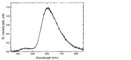
- 2 is an emission spectrum of an organic electroluminescence device using Compound 1 of Example 3.
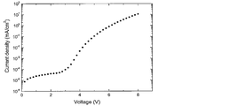
- 4 is a graph showing current density-voltage characteristics of an organic electroluminescence device using Compound 1 of Example 3.
- 2 is an emission spectrum of an organic electroluminescence device using the compound 2 of Example 3.
- 6 is a graph showing current density-voltage characteristics of an organic electroluminescence device using Compound 2 of Example 3.
- 6 is a graph showing luminance-external quantum efficiency characteristics of an organic electroluminescence device using the compound 2 of Example 3.
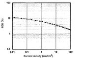
- 6 is a graph showing current density-external quantum efficiency characteristics of an organic electroluminescence device using Compound 2 of Example 3.
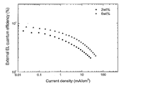
- 6 is a graph showing current density-external quantum efficiency characteristics of an organic electroluminescence device using the compound 6 of Example 3.
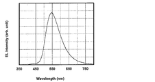
- 2 is an emission spectrum of an organic electroluminescence device using the compound 6 of Example 3.
- 6 is a graph showing current density-voltage characteristics of an organic electroluminescence device using the compound 6 of Example 3.
- 6 is a graph showing current density-external quantum efficiency characteristics of an organic electroluminescence device using the compound 6 of Example 3.
- a numerical range represented by using “to” means a range including numerical values described before and after “to” as a lower limit value and an upper limit value.
- the isotope species of the hydrogen atom present in the molecule of the compound used in the present invention is not particularly limited. For example, all the hydrogen atoms in the molecule may be 1 H, or a part or all of them are 2 H. (Deuterium D) may be used.
- D represents the bivalent group containing the structure represented by a following formula.
- the hydrogen atom present in the above structure may be substituted with a substituent.
- the number of substituents is not particularly limited, and the substituents may not be present. When two or more substituents are present, these substituents may be the same as or different from each other.
- substituents examples include a hydroxy group, a halogen atom, an alkyl group having 1 to 20 carbon atoms, an alkoxy group having 1 to 20 carbon atoms, an alkylthio group having 1 to 20 carbon atoms, an aryl group having 6 to 40 carbon atoms, and a carbon number.
- Examples thereof include 20 trialkylsilylalkyl groups, 5 to 20 trialkylsilylalkenyl groups, and 5 to 20 trialkylsilylalkynyl groups.
- those that can be substituted with a substituent may be further substituted.
- substituents are substituted or unsubstituted alkyl groups having 1 to 20 carbon atoms, alkoxy groups having 1 to 20 carbon atoms, substituted or unsubstituted aryl groups having 6 to 40 carbon atoms, and substituted groups having 3 to 40 carbon atoms. Or it is an unsubstituted heteroaryl group.
- Further preferred substituents are substituted or unsubstituted alkyl groups having 1 to 10 carbon atoms, substituted or unsubstituted alkoxy groups having 1 to 10 carbon atoms, substituted or unsubstituted aryl groups having 6 to 15 carbon atoms, 3 to 12 substituted or unsubstituted heteroaryl groups.
- the alkyl group may be linear, branched or cyclic, and more preferably has 1 to 6 carbon atoms. Specific examples include a methyl group, an ethyl group, a propyl group, a butyl group, and tert-butyl. Group, pentyl group, hexyl group and isopropyl group.
- the alkoxy group may be linear, branched or cyclic, and more preferably has 1 to 6 carbon atoms. Specific examples thereof include methoxy group, ethoxy group, propoxy group, butoxy group, tert-butoxy group. A group, a pentyloxy group, a hexyloxy group, and an isopropyloxy group.
- the aryl group that can be employed as the substituent may be a single ring or a condensed ring, and specific examples thereof include a phenyl group and a naphthyl group.
- the heteroaryl group may be a single ring or a condensed ring, and specific examples thereof include a pyridyl group, a pyridazyl group, a pyrimidyl group, a triazyl group, a triazolyl group, and a benzotriazolyl group.
- These heteroaryl groups may be a group bonded through a hetero atom or a group bonded through a carbon atom constituting a heteroaryl ring.
- D in the general formula (1) is preferably a group having a structure represented by the following general formula (2).
- R 1 to R 8 each independently represents a hydrogen atom or a substituent.
- R 1 to R 8 may all be hydrogen atoms.
- those substituents may be the same or different.
- R 1 and R 2 , R 2 and R 3 , R 3 and R 4 , R 5 and R 6 , R 6 and R 7 , and R 7 and R 8 may be bonded to each other to form a cyclic structure.
- the cyclic structure may be an aromatic ring or an alicyclic ring, may contain a hetero atom, and the cyclic structure may be a condensed ring of two or more rings.
- the hetero atom here is preferably selected from the group consisting of a nitrogen atom, an oxygen atom and a sulfur atom.
- Examples of cyclic structures formed include benzene ring, naphthalene ring, pyridine ring, pyridazine ring, pyrimidine ring, pyrazine ring, pyrrole ring, imidazole ring, pyrazole ring, triazole ring, imidazoline ring, oxazole ring, isoxazole ring, thiazole And a ring, an isothiazole ring, a cyclohexadiene ring, a cyclohexene ring, a cyclopentaene ring, a cycloheptatriene ring, a cycloheptadiene ring, and a cycloheptaene ring.
- Preferable examples of the structure represented by the general formula (2) include a structure in which R 1 to R 8 are all hydrogen atoms. Also, R 1 and R 8 , R 2 and R 7 , R 3 and R 6 , R 4 and R 5 are the same line symmetrical structure, R 1 and R 5 , R 2 and R 6 , R 3 And a rotationally symmetric structure in which R 7 and R 4 and R 8 are the same.
- A represents a group having a structure selected from the following group.
- Each hydrogen atom present in the structure described in the above group may be substituted with a substituent.
- the number of substituents is not particularly limited, and the substituents may not be present. When two or more substituents are present, these substituents may be the same as or different from each other.
- Examples of the substituent that can replace a hydrogen atom present in the structure described in the above group include a hydroxy group, a halogen atom, a cyano group, an alkyl group having 1 to 20 carbon atoms, and an alkoxy group having 1 to 20 carbon atoms.
- alkylthio group having 1 to 20 carbon atoms an alkyl-substituted amino group having 1 to 20 carbon atoms, an aryl-substituted amino group having 12 to 40 carbon atoms, an acyl group having 2 to 20 carbon atoms, an aryl group having 6 to 40 carbon atoms, Heteroaryl group having 3 to 40 carbon atoms, substituted or unsubstituted carbazolyl group having 12 to 40 carbon atoms, alkenyl group having 2 to 10 carbon atoms, alkynyl group having 2 to 10 carbon atoms, alkoxycarbonyl having 2 to 10 carbon atoms Groups, alkylsulfonyl groups having 1 to 10 carbon atoms, haloalkyl groups having 1 to 10 carbon atoms, amide groups, alkylamide groups having 2 to 10 carbon atoms, and trials having 3 to 20 carbon atoms Rushiriru group, trialkylsilyl group having 4-20 carbon atoms
- substituents are a halogen atom, a cyano group, a substituted or unsubstituted alkyl group having 1 to 20 carbon atoms, an alkoxy group having 1 to 20 carbon atoms, a substituted or unsubstituted aryl group having 6 to 40 carbon atoms, carbon A substituted or unsubstituted heteroaryl group having 3 to 40 carbon atoms, a substituted or unsubstituted dialkylamino group having 1 to 10 carbon atoms, a substituted or unsubstituted diarylamino group having 12 to 40 carbon atoms, and 12 to 40 carbon atoms A substituted or unsubstituted carbazolyl group; More preferred substituents are a fluorine atom, a chlorine atom, a cyano group, a substituted or unsubstituted alkyl group having 1 to 10 carbon atoms
- an unsubstituted dialkylamino group a substituted or unsubstituted diarylamino group having 12 to 40 carbon atoms, a substituted or unsubstituted aryl group having 6 to 15 carbon atoms, and a substituted or unsubstituted heteroaryl group having 3 to 12 carbon atoms It is a group.
- the hydrogen atoms bonded to adjacent ring skeleton atoms present in the structure described in the above group may be bonded to each other to form a cyclic structure.
- the cyclic structure may be an aromatic ring or an alicyclic ring, may contain a hetero atom, and the cyclic structure may be a condensed ring of two or more rings.
- the two A in the general formula (1) may be the same or different from each other, but are preferably the same.
- the whole molecule is preferably line symmetric or point symmetric.
- Ordinary luminescent materials have an AD structure in which A acting as an acceptor and D acting as a donor are combined.
- the compound represented by the general formula (1) has a structure of ADA, and two A acting as an acceptor are bonded to D acting as a donor.
- a and D when two or more A's are bonded, there is a general concern that the function as an acceptor cancels and there is a risk that the molecule does not function effectively as a luminescent material.
- a and D in accordance with the present invention, a light emitting material having high luminous efficiency and excellent effects can be provided. This is presumably because the HOMO and LUMO spreads were controlled at the molecular level to satisfy the preferable conditions for the light-emitting material.
- the compound represented by the general formula (1) is preferably a compound having a structure represented by the following general formula (3).
- R 1 to R 8 and R 11 to R 20 each independently represents a hydrogen atom or a substituent.
- R 1 and R 2 , R 2 and R 3 , R 3 and R 4 , R 5 and R 6 , R 6 and R 7 , R 7 and R 8 , R 11 and R 12 , R 12 and R 13 , R 13 And R 14 , R 14 and R 15 , R 16 and R 17 , R 17 and R 18 , R 18 and R 19 , and R 19 and R 20 may be bonded to each other to form a cyclic structure.
- the substituents that R 1 to R 8 can take the corresponding description of the general formula (1) can be referred to.
- R 12 is a cyano group or a group having the following structure (however, a hydrogen atom may be substituted with a substituent)
- R 13 is a cyano group or a group having any structure of the following group (wherein a hydrogen atom may be substituted with a substituent)
- R 17 is a cyano group or a group having the following structure (however, a hydrogen atom may be substituted with a substituent), R 18 is a cyano group or a group of any of the following groups (wherein a hydrogen atom may be substituted with a substituent), or R 17 and R 18 are bonded to each other, and together with the benzene ring to which R 17 and R 18 are bonded, a group that forms one of the following structures (however, a hydrogen atom may be substituted with a substituent) ).
- R 1 to R 8 in the general formula (3) are each independently a hydrogen atom, a substituted or unsubstituted alkyl group having 1 to 10 carbon atoms, a substituted or unsubstituted alkoxy group having 1 to 10 carbon atoms, a carbon number of 6
- a substituted or unsubstituted aryl group having 15 to 15 carbon atoms and a substituted or unsubstituted heteroaryl group having 3 to 12 carbon atoms are preferable.
- R 12 , R 13 , R 17 and R 18 in the general formula (3) have a substituent so as to satisfy the above conditions ⁇ 1> and ⁇ 2>.
- R 11 to R 18 are each independently a hydrogen atom, a fluorine atom, a chlorine atom, a cyano group, a substituted or unsubstituted alkyl group having 1 to 10 carbon atoms, a substituted or unsubstituted alkoxy group having 1 to 10 carbon atoms, carbon A substituted or unsubstituted dialkylamino group having 1 to 10 carbon atoms, a substituted or unsubstituted diarylamino group having 12 to 40 carbon atoms, a substituted or unsubstituted aryl group having 6 to 15 carbon atoms, or 3 to 12 carbon atoms It is preferably a substituted or unsubstituted heteroaryl group.
- the substituent in which the hydrogen atom having the structure described in the above ⁇ 1> and ⁇ 2> in the general formula (3) may be substituted is a fluorine atom, a chlorine atom, a cyano group, or a group having 1 to 10 carbon atoms.
- Substituted or unsubstituted alkyl group substituted or unsubstituted alkoxy group having 1 to 10 carbon atoms, substituted or unsubstituted dialkylamino group having 1 to 10 carbon atoms, substituted or unsubstituted diarylamino group having 12 to 40 carbon atoms It is preferably selected from the group consisting of a group, a substituted or unsubstituted aryl group having 6 to 15 carbon atoms, and a substituted or unsubstituted heteroaryl group having 3 to 12 carbon atoms.
- the molecular weight of the compound represented by the general formula (1) is, for example, 1500 or less when the organic layer containing the compound represented by the general formula (1) is intended to be formed by vapor deposition. Preferably, it is preferably 1200 or less, more preferably 1000 or less, and even more preferably 800 or less.
- the lower limit of the molecular weight is the molecular weight of the minimum compound represented by the general formula (1).
- the compound represented by the general formula (1) may be formed by a coating method regardless of the molecular weight. If a coating method is used, a film can be formed even with a compound having a relatively large molecular weight.
- a compound containing a plurality of structures represented by the general formula (1) in the molecule as a light emitting material.
- a polymer obtained by previously polymerizing a polymerizable group in the structure represented by the general formula (1) and polymerizing the polymerizable group as a light emitting material.
- a repeating unit is prepared by preparing a monomer containing a polymerizable functional group in either A or D of the general formula (1) and polymerizing the monomer alone or copolymerizing with another monomer. It is conceivable to obtain a polymer having the above and use the polymer as a light emitting material.
- dimers and trimers are obtained by reacting compounds having a structure represented by the general formula (1) and used as a luminescent material.
- Examples of the polymer having a repeating unit containing a structure represented by the general formula (1) include a polymer containing a structure represented by the following general formula (4) or (5).
- Q represents a group including the structure represented by the general formula (1)
- L 1 and L 2 represent a linking group.
- the linking group preferably has 0 to 20 carbon atoms, more preferably 1 to 15 carbon atoms, and still more preferably 2 to 10 carbon atoms. And preferably has a structure represented by - linking group -X 11 -L 11.
- X 11 represents an oxygen atom or a sulfur atom, and is preferably an oxygen atom.
- L 11 represents a linking group, preferably a substituted or unsubstituted alkylene group, or a substituted or unsubstituted arylene group, and a substituted or unsubstituted alkylene group having 1 to 10 carbon atoms, or a substituted or unsubstituted group A phenylene group is more preferable.
- R 101 , R 102 , R 103 and R 104 each independently represent a substituent.
- it is a substituted or unsubstituted alkyl group having 1 to 6 carbon atoms, a substituted or unsubstituted alkoxy group having 1 to 6 carbon atoms, or a halogen atom, more preferably an unsubstituted alkyl group having 1 to 3 carbon atoms.
- An unsubstituted alkoxy group having 1 to 3 carbon atoms, a fluorine atom, and a chlorine atom and more preferably an unsubstituted alkyl group having 1 to 3 carbon atoms and an unsubstituted alkoxy group having 1 to 3 carbon atoms.
- the linking group represented by L 1 and L 2 is any one of A or D in the structure of the general formula (1) constituting R and R 1 to R 8 and R 11 to R 18 in the structure of the general formula (3). Can be combined. Two or more linking groups may be linked to one Q to form a crosslinked structure or a network structure.
- repeating unit examples include structures represented by the following formulas (6) to (9).
- a hydroxy group is introduced into either A or D of the structure of the general formula (1), and the following compound is used as a linker: It can be synthesized by reacting to introduce a polymerizable group and polymerizing the polymerizable group.
- the polymer containing a structure represented by the general formula (1) in the molecule may be a polymer consisting only of a repeating unit having the structure represented by the general formula (1), or other structures may be used. It may be a polymer containing repeating units.
- the repeating unit having a structure represented by the general formula (1) contained in the polymer may be a single type or two or more types. Examples of the repeating unit not having the structure represented by the general formula (1) include those derived from monomers used in ordinary copolymerization. Examples thereof include a repeating unit derived from a monomer having an ethylenically unsaturated bond such as ethylene and styrene.
- the compound represented by the general formula (1) can be synthesized by combining known reactions. For example, it can be synthesized according to the following scheme. For the explanation of D and A in the above formula, the corresponding description in the general formula (1) can be referred to.
- X in the above formula represents a halogen atom, and examples thereof include a fluorine atom, a chlorine atom, a bromine atom and an iodine atom, and a chlorine atom, a bromine atom and an iodine atom are preferable.
- the compound represented by the general formula (3) can be synthesized by the following scheme. However, the scheme described below shows a synthesis method when R 11 and R 16 , R 12 and R 17 , R 13 and R 18 , R 14 and R 19 , and R 15 and R 20 are the same. is there.
- R 1 to R 8 and R 11 to R 20 in the above formula the corresponding description in the general formula (3) can be referred to.
- X in the above formula represents a halogen atom.
- the reactions in the above two schemes apply known reactions, and known reaction conditions can be appropriately selected and used. The details of the above reaction can be referred to the synthesis examples described below.
- the compound represented by the general formula (1) can also be synthesized by combining other known synthesis reactions.
- the compound represented by the general formula (1) of the present invention is useful as a light emitting material of an organic light emitting device. For this reason, the compound represented by General formula (1) of this invention can be effectively used as a luminescent material for the light emitting layer of an organic light emitting element.
- the compound represented by the general formula (1) includes a delayed fluorescent material (delayed phosphor) that emits delayed fluorescence. That is, the present invention relates to a delayed phosphor having a structure represented by the general formula (1), an invention using a compound represented by the general formula (1) as a delayed phosphor, and a general formula (1).
- An invention of a method for emitting delayed fluorescence using the represented compound is also provided.
- An organic light emitting device using such a compound as a light emitting material emits delayed fluorescence and has a feature of high luminous efficiency. The principle will be described below by taking an organic electroluminescence element as an example.
- the organic electroluminescence element carriers are injected into the light emitting material from both positive and negative electrodes to generate an excited light emitting material and emit light.
- 25% of the generated excitons are excited to the excited singlet state, and the remaining 75% are excited to the excited triplet state. Therefore, the use efficiency of energy is higher when phosphorescence, which is light emission from an excited triplet state, is used.
- the excited triplet state has a long lifetime, energy saturation occurs due to saturation of the excited state and interaction with excitons in the excited triplet state, and in general, the quantum yield of phosphorescence is often not high.
- delayed fluorescent materials after energy transition to an excited triplet state due to intersystem crossing, etc., are then crossed back to an excited singlet state due to triplet-triplet annihilation or absorption of thermal energy, and emit fluorescence.
- a thermally activated delayed fluorescent material by absorption of thermal energy is particularly useful.
- excitons in the excited singlet state emit fluorescence as usual.
- excitons in the excited triplet state absorb heat generated by the device and cross between the excited singlets to emit fluorescence.
- the light is emitted from the excited singlet, the light is emitted at the same wavelength as the fluorescence, but the light lifetime (luminescence lifetime) generated by the reverse intersystem crossing from the excited triplet state to the excited singlet state is normal. Since the fluorescence becomes longer than the fluorescence and phosphorescence, it is observed as fluorescence delayed from these. This can be defined as delayed fluorescence. If such a heat-activated exciton transfer mechanism is used, the ratio of the compound in an excited singlet state, which normally generated only 25%, is increased to 25% or more by absorbing thermal energy after carrier injection. It can be raised.
- the heat of the device will sufficiently cause intersystem crossing from the excited triplet state to the excited singlet state and emit delayed fluorescence. Efficiency can be improved dramatically.
- the compound represented by the general formula (1) of the present invention as a light-emitting material of a light-emitting layer, excellent organic light-emitting devices such as an organic photoluminescence device (organic PL device) and an organic electroluminescence device (organic EL device) Can be provided.
- the compound represented by the general formula (1) of the present invention may have a function of assisting light emission of another light emitting material included in the light emitting layer as a so-called assist dopant. That is, the compound represented by the general formula (1) of the present invention contained in the light emitting layer includes the lowest excitation singlet energy level of the host material contained in the light emitting layer and the lowest excitation of other light emitting materials contained in the light emitting layer.
- the organic photoluminescence element has a structure in which at least a light emitting layer is formed on a substrate.
- the organic electroluminescence element has a structure in which an organic layer is formed at least between an anode, a cathode, and an anode and a cathode.
- the organic layer includes at least a light emitting layer, and may consist of only the light emitting layer, or may have one or more organic layers in addition to the light emitting layer. Examples of such other organic layers include a hole transport layer, a hole injection layer, an electron blocking layer, a hole blocking layer, an electron injection layer, an electron transport layer, and an exciton blocking layer.
- the hole transport layer may be a hole injection / transport layer having a hole injection function
- the electron transport layer may be an electron injection / transport layer having an electron injection function.
- FIG. 1 A specific example of the structure of an organic electroluminescence element is shown in FIG.
- 1 is a substrate
- 2 is an anode
- 3 is a hole injection layer
- 4 is a hole transport layer
- 5 is a light emitting layer
- 6 is an electron transport layer
- 7 is a cathode.
- each member and each layer of an organic electroluminescent element are demonstrated.
- substrate and a light emitting layer corresponds also to the board
- the organic electroluminescence device of the present invention is preferably supported on a substrate.
- the substrate is not particularly limited and may be any substrate conventionally used for organic electroluminescence elements.
- a substrate made of glass, transparent plastic, quartz, silicon, or the like can be used.
- an electrode material made of a metal, an alloy, an electrically conductive compound, or a mixture thereof having a high work function (4 eV or more) is preferably used.
- electrode materials include metals such as Au, and conductive transparent materials such as CuI, indium tin oxide (ITO), SnO 2 , and ZnO.
- conductive transparent materials such as CuI, indium tin oxide (ITO), SnO 2 , and ZnO.
- an amorphous material such as IDIXO (In 2 O 3 —ZnO) that can form a transparent conductive film may be used.
- a thin film may be formed by vapor deposition or sputtering of these electrode materials, and a pattern of a desired shape may be formed by photolithography, or when pattern accuracy is not so high (about 100 ⁇ m or more) ), A pattern may be formed through a mask having a desired shape at the time of vapor deposition or sputtering of the electrode material.
- wet film-forming methods such as a printing system and a coating system, can also be used.
- the transmittance be greater than 10%, and the sheet resistance as the anode is preferably several hundred ⁇ / ⁇ or less.
- the film thickness depends on the material, it is usually selected in the range of 10 to 1000 nm, preferably 10 to 200 nm.
- cathode a material having a low work function (4 eV or less) metal (referred to as an electron injecting metal), an alloy, an electrically conductive compound, and a mixture thereof as an electrode material is used.
- electrode materials include sodium, sodium-potassium alloy, magnesium, lithium, magnesium / copper mixture, magnesium / silver mixture, magnesium / aluminum mixture, magnesium / indium mixture, aluminum / aluminum oxide (Al 2 O 3 ) Mixtures, indium, lithium / aluminum mixtures, rare earth metals and the like.
- a mixture of an electron injecting metal and a second metal which is a stable metal having a larger work function value than this for example, a magnesium / silver mixture
- Suitable are a magnesium / aluminum mixture, a magnesium / indium mixture, an aluminum / aluminum oxide (Al 2 O 3 ) mixture, a lithium / aluminum mixture, aluminum and the like.
- the cathode can be produced by forming a thin film of these electrode materials by a method such as vapor deposition or sputtering.
- the sheet resistance as the cathode is preferably several hundred ⁇ / ⁇ or less, and the film thickness is usually selected in the range of 10 nm to 5 ⁇ m, preferably 50 to 200 nm.
- the emission luminance is advantageously improved.
- a transparent or semi-transparent cathode can be produced. By applying this, an element in which both the anode and the cathode are transparent is used. Can be produced.
- the light emitting layer is a layer that emits light after excitons are generated by recombination of holes and electrons injected from each of the anode and the cathode, and the light emitting material may be used alone for the light emitting layer. , Preferably including a luminescent material and a host material.
- a luminescent material the 1 type (s) or 2 or more types chosen from the compound group of this invention represented by General formula (1) can be used.
- a host material in addition to the light emitting material in the light emitting layer.
- the host material an organic compound having at least one of excited singlet energy and excited triplet energy higher than that of the light emitting material of the present invention can be used.
- singlet excitons and triplet excitons generated in the light emitting material of the present invention can be confined in the molecules of the light emitting material of the present invention, and the light emission efficiency can be sufficiently extracted.
- high luminous efficiency can be obtained, so that host materials that can achieve high luminous efficiency are particularly limited. And can be used in the present invention.
- the organic light emitting device or organic electroluminescent device of the present invention light emission is generated from the light emitting material of the present invention contained in the light emitting layer.
- This emission includes both fluorescence and delayed fluorescence.
- part of the light emission may include light emission from the host material.
- the amount of the compound of the present invention, which is a light emitting material is preferably 0.1% by weight or more, more preferably 1% by weight or more, and 50% or more. It is preferably no greater than wt%, more preferably no greater than 20 wt%, and even more preferably no greater than 10 wt%.
- the host material in the light-emitting layer is preferably an organic compound that has a hole transporting ability and an electron transporting ability, prevents the emission of longer wavelengths, and has a high glass transition temperature.
- the injection layer is a layer provided between the electrode and the organic layer for lowering the driving voltage and improving the luminance of light emission.
- the injection layer can be provided as necessary.
- the blocking layer is a layer that can prevent diffusion of charges (electrons or holes) and / or excitons existing in the light emitting layer to the outside of the light emitting layer.
- the electron blocking layer can be disposed between the light emitting layer and the hole transport layer and blocks electrons from passing through the light emitting layer toward the hole transport layer.
- a hole blocking layer can be disposed between the light emitting layer and the electron transporting layer to prevent holes from passing through the light emitting layer toward the electron transporting layer.
- the blocking layer can also be used to block excitons from diffusing outside the light emitting layer. That is, each of the electron blocking layer and the hole blocking layer can also function as an exciton blocking layer.
- the term “electron blocking layer” or “exciton blocking layer” as used herein is used in the sense of including a layer having the functions of an electron blocking layer and an exciton blocking layer in one layer.
- the hole blocking layer has a function of an electron transport layer in a broad sense.
- the hole blocking layer has a role of blocking holes from reaching the electron transport layer while transporting electrons, thereby improving the recombination probability of electrons and holes in the light emitting layer.
- the material for the hole blocking layer the material for the electron transport layer described later can be used as necessary.
- the electron blocking layer has a function of transporting holes in a broad sense.
- the electron blocking layer has a role to block electrons from reaching the hole transport layer while transporting holes, thereby improving the probability of recombination of electrons and holes in the light emitting layer. .
- the exciton blocking layer is a layer for preventing excitons generated by recombination of holes and electrons in the light emitting layer from diffusing into the charge transport layer. It becomes possible to efficiently confine in the light emitting layer, and the light emission efficiency of the device can be improved.
- the exciton blocking layer can be inserted on either the anode side or the cathode side adjacent to the light emitting layer, or both can be inserted simultaneously.
- the layer when the exciton blocking layer is provided on the anode side, the layer can be inserted adjacent to the light emitting layer between the hole transport layer and the light emitting layer, and when inserted on the cathode side, the light emitting layer and the cathode Between the luminescent layer and the light-emitting layer.
- a hole injection layer, an electron blocking layer, or the like can be provided between the anode and the exciton blocking layer adjacent to the anode side of the light emitting layer, and the excitation adjacent to the cathode and the cathode side of the light emitting layer can be provided.
- an electron injection layer, an electron transport layer, a hole blocking layer, and the like can be provided.
- the blocking layer is disposed, at least one of the excited singlet energy and the excited triplet energy of the material used as the blocking layer is preferably higher than the excited singlet energy and the excited triplet energy of the light emitting material.
- the hole transport layer is made of a hole transport material having a function of transporting holes, and the hole transport layer can be provided as a single layer or a plurality of layers.
- the hole transport material has any one of hole injection or transport and electron barrier properties, and may be either organic or inorganic.
- hole transport materials that can be used include, for example, triazole derivatives, oxadiazole derivatives, imidazole derivatives, carbazole derivatives, indolocarbazole derivatives, polyarylalkane derivatives, pyrazoline derivatives and pyrazolone derivatives, phenylenediamine derivatives, arylamine derivatives, Examples include amino-substituted chalcone derivatives, oxazole derivatives, styrylanthracene derivatives, fluorenone derivatives, hydrazone derivatives, stilbene derivatives, silazane derivatives, aniline copolymers, and conductive polymer oligomers, particularly thiophene oligomers.
- An aromatic tertiary amine compound and an styrylamine compound are preferably used, and an aromatic tertiary amine compound is more preferably used.
- the electron transport layer is made of a material having a function of transporting electrons, and the electron transport layer can be provided as a single layer or a plurality of layers.
- the electron transport material (which may also serve as a hole blocking material) may have a function of transmitting electrons injected from the cathode to the light emitting layer.
- Examples of the electron transport layer that can be used include nitro-substituted fluorene derivatives, diphenylquinone derivatives, thiopyran dioxide oxide derivatives, carbodiimides, fluorenylidenemethane derivatives, anthraquinodimethane and anthrone derivatives, oxadiazole derivatives, and the like.
- a thiadiazole derivative in which the oxygen atom of the oxadiazole ring is substituted with a sulfur atom, and a quinoxaline derivative having a quinoxaline ring known as an electron withdrawing group can also be used as an electron transport material.
- a polymer material in which these materials are introduced into a polymer chain or these materials are used as a polymer main chain can also be used.
- the compound represented by the general formula (1) may be used not only for the light emitting layer but also for layers other than the light emitting layer.
- the compound represented by General formula (1) used for a light emitting layer and the compound represented by General formula (1) used for layers other than a light emitting layer may be same or different.
- the compound represented by the general formula (1) may be used for the injection layer, blocking layer, hole blocking layer, electron blocking layer, exciton blocking layer, hole transporting layer, electron transporting layer, and the like. .
- the method for forming these layers is not particularly limited, and the layer may be formed by either a dry process or a wet process.
- the preferable material which can be used for an organic electroluminescent element is illustrated concretely.
- the material that can be used in the present invention is not limited to the following exemplary compounds. Moreover, even if it is a compound illustrated as a material which has a specific function, it can also be diverted as a material which has another function.
- R and R 2 to R 7 each independently represent a hydrogen atom or a substituent.
- n represents an integer of 3 to 5.
- the organic electroluminescence device produced by the above-described method emits light by applying an electric field between the anode and the cathode of the obtained device. At this time, if the light is emitted by excited singlet energy, light having a wavelength corresponding to the energy level is confirmed as fluorescence emission and delayed fluorescence emission. In addition, in the case of light emission by excited triplet energy, a wavelength corresponding to the energy level is confirmed as phosphorescence. Since normal fluorescence has a shorter fluorescence lifetime than delayed fluorescence, the emission lifetime can be distinguished from fluorescence and delayed fluorescence.
- the excited triplet energy is unstable and is converted into heat and the like, and the lifetime is short and it is immediately deactivated.
- the excited triplet energy of a normal organic compound it can be measured by observing light emission under extremely low temperature conditions.
- the organic electroluminescence element of the present invention can be applied to any of a single element, an element having a structure arranged in an array, and a structure in which an anode and a cathode are arranged in an XY matrix.
- an organic light emitting device with greatly improved light emission efficiency can be obtained by containing the compound represented by the general formula (1) in the light emitting layer.
- the organic light emitting device such as the organic electroluminescence device of the present invention can be further applied to various uses. For example, it is possible to produce an organic electroluminescence display device using the organic electroluminescence element of the present invention. For details, see “Organic EL Display” (Ohm Co., Ltd.) ) Can be referred to.
- the organic electroluminescence device of the present invention can be applied to organic electroluminescence illumination and backlights that are in great demand.
- the maximum point having a peak intensity of 10% or less of the maximum peak intensity of the spectrum is not included in the above-mentioned maximum value on the shortest wavelength side, and has the maximum slope value closest to the maximum value on the shortest wavelength side.
- the tangent drawn at the point where the value was taken was taken as the tangent to the rising edge of the phosphorescence spectrum on the short wavelength side.
- Example 1 Preparation and evaluation of organic photoluminescence device (solution)
- a toluene solution concentration 10 ⁇ 5 mol / L
- Compound 1 synthesized in Synthesis Example 1 was prepared and irradiated with ultraviolet light at 300 K while bubbling nitrogen, fluorescence at 586 nm was observed.
- the photoluminescence quantum efficiency in the toluene solution before and after the nitrogen bubble was measured at 300 K with an absolute PL quantum yield measurement device (Quantaurus-QY manufactured by Hamamatsu Photonics Co., Ltd.), it was 3.4% before the nitrogen bubble. Yes, 5.5% after nitrogen bubble.
- the photoluminescence quantum efficiency was 1.9% before the nitrogen bubble and 2.3% after the nitrogen bubble.
- the photoluminescence quantum efficiency was 4.7% before the nitrogen bubble and 9.7% after the nitrogen bubble.
- Example 2 Preparation and evaluation of organic photoluminescence device (thin film)
- FIG. 2 shows transient attenuation curves at temperatures of 50K, 100K, 150K, 200K, 250K, and 300K. It was confirmed that Compound 1 is a thermally activated delayed fluorescent material.
- ⁇ p at 300 K was 6.24 ns
- ⁇ d was 0.14 ⁇ s.
- FIG. 3 shows transient attenuation curves at respective temperatures of 50K, 100K, 150K, 200K, 250K, and 300K.
- Compound 2 was confirmed to be a thermally activated delayed fluorescent material.
- ⁇ p at 300 K was 6.83 ns
- ⁇ d was 6.69 ⁇ s.
- the photoluminescence quantum efficiency obtained using the same measuring apparatus as in Example 1 was 35.2% at 300 K (normal fluorescence 16.8%, delayed fluorescence 18.4%).
- ⁇ E ST was 0.10 eV.
- An organic photoluminescence device was prepared using Compound 5 instead of Compound 1, and the measurement was performed in the same manner.
- FIG. 3 shows transient attenuation curves at respective temperatures of 50K, 100K, 150K, 200K, 250K, and 300K.
- Compound 2 was confirmed to be a thermally activated delayed fluorescent material.
- ⁇ p at 300 K was 6.83 ns
- ⁇ d was 6.69 ⁇ s.
- FIG. 4 shows transient attenuation curves at respective temperatures of 50K, 100K, 150K, 200K, 250K, and 300K.
- Compound 5 was confirmed to be a thermally activated delayed fluorescent material.
- ⁇ p at 300 K was 12.18 ns and ⁇ d was 1.10 ⁇ s.
- the photoluminescence quantum efficiency obtained using the same measuring apparatus as Example 1 was 33.0% at 300K (normal fluorescence 20.6%, delayed fluorescence 12.4%).
- ⁇ E ST was 0.03 eV.
- An organic photoluminescence device was prepared using Compound 6 instead of Compound 1, and the measurement was performed in the same manner.
- FIG. 5 shows transient attenuation curves at respective temperatures of 50K, 100K, 150K, 200K, 250K, and 300K.
- Compound 6 was confirmed to be a thermally activated delayed fluorescent material.
- ⁇ p at 300 K was 4.12 ns, and ⁇ d was 53.00 ⁇ s.
- the photoluminescence quantum efficiency obtained using the same measuring apparatus as in Example 1 was 67.6% at 300 K (normal fluorescence 34.0%, delayed fluorescence 33.6%).
- ⁇ E ST was 0.19 eV.
- Example 3 Production and Evaluation of Organic Electroluminescence Element
- ITO indium tin oxide
- Lamination was performed at 0 ⁇ 10 ⁇ 4 Pa.
- ⁇ -NPD was formed on ITO to a thickness of 35 nm.
- Compound 1 and CBP were co-deposited from different vapor deposition sources to form a layer having a thickness of 15 nm as a light emitting layer. At this time, the concentration of Compound 1 was 2.0% by weight.
- TPBi is formed to a thickness of 65 nm
- further lithium fluoride (LiF) is vacuum-deposited to a thickness of 0.5 nm
- aluminum (Al) is evaporated to a thickness of 100 nm to form a cathode.
- a luminescence element was obtained.
- a semiconductor parameter analyzer manufactured by Agilent Technologies: E5273A
- an optical power meter measuring device manufactured by Newport: 1930C
- an optical spectrometer manufactured by Ocean Optics: USB2000
- the compound 2 is used in place of the compound 1, and the organic electroluminescence device having the concentration of the compound 2 in the light emitting layer of 2.0% by weight and the organic electroluminescent element having the concentration of the compound 2 in the light emitting layer of 6.0% by weight.
- a luminescence element was produced.
- the emission spectrum is shown in FIG. 8, the current density-voltage characteristic is shown in FIG. 9, the luminance-external quantum efficiency characteristic is shown in FIG. 10, and the current density-external quantum efficiency characteristic is shown in FIG.
- the organic electroluminescence device using Compound 2 as the light emitting material achieved a high external quantum efficiency of 8.8%.
- FIG. 13 shows the emission spectrum
- FIG. 14 shows the current density-voltage characteristics
- FIG. 15 shows the current density-external quantum efficiency characteristics.
- the organic electroluminescence device using Compound 6 as the light emitting material achieved a high external quantum efficiency of 11.3%.
- FIG. 12 shows the current density-external quantum efficiency characteristics when an organic electroluminescent device having a concentration of compound 6 in the light emitting layer of 6.0% by weight was produced. This organic electroluminescence device achieved a high external quantum efficiency of 12.1%.
- the compound of the present invention is useful as a luminescent material. For this reason, the compound of this invention is effectively used as a luminescent material for organic light emitting elements, such as an organic electroluminescent element. Since the compounds of the present invention include those that emit delayed fluorescence, it is also possible to provide an organic light emitting device with high luminous efficiency. For this reason, this invention has high industrial applicability.
Abstract
A-D-Aで表される化合物は、発光材料として有用である。
Description
本発明は、発光材料として有用な化合物とそれを用いた有機発光素子に関する。
有機エレクトロルミネッセンス素子(有機EL素子)などの有機発光素子の発光効率を高める研究が盛んに行われている。特に、有機エレクトロルミネッセンス素子を構成する電子輸送材料、正孔輸送材料、発光材料などを新たに開発して組み合わせることにより、発光効率を高める工夫が種々なされてきている。その中には、フェナジン構造を含む化合物を利用した有機エレクトロルミネッセンス素子に関する研究も見受けられ、これまでにも幾つかの提案がなされてきている。
例えば特許文献1には、発光素子を構成する一対の電極間に存在する有機層の中に、下記の一般式で表されるフェナジン構造を含む化合物を用いることが記載されている。下記の一般式において、R1およびR2は置換もしくは無置換のアリール基、または置換もしくは無置換の複素環基であることが規定されている。
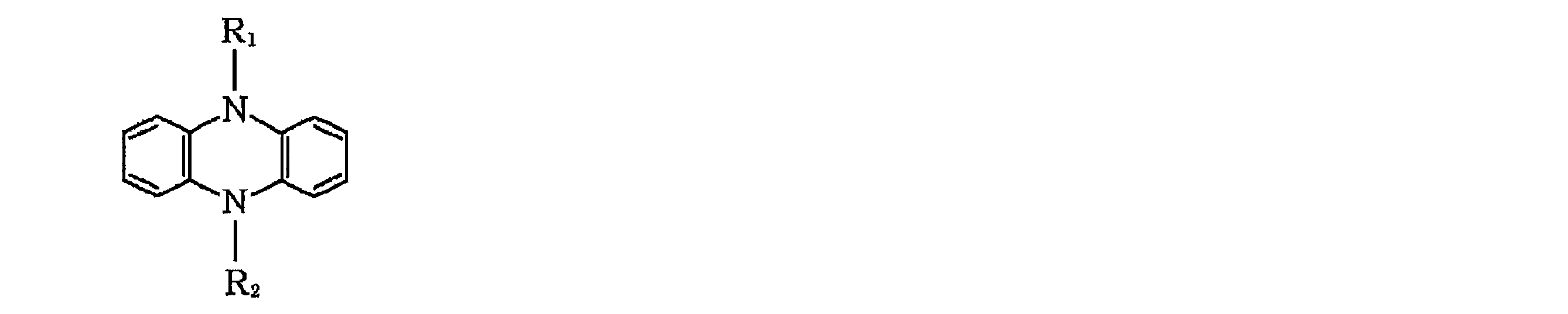
特許文献1の中には、R1およびR2として広範囲な構造を包含する一般式が記載されているが、具体的な構造は8つしか記載されていない。実施例ではそのうち7つの化合物を用いた発光素子について、発光することが確認されており、なかでも下記の構造を有する化合物を用いた発光素子が比較的良好な輝度と耐久性を有することが示されている。
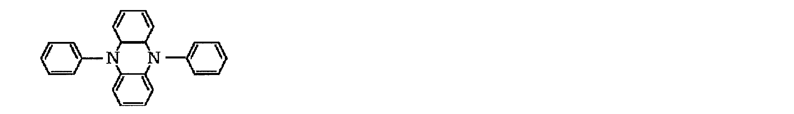
このようにフェナジン構造等を含む化合物については、これまでに有機エレクトロルミネッセンス素子への応用に関する提案がなされている。しかしながら、フェナジン骨格を形成する窒素原子に結合しているアリール基に、さらにトリアジン環、ベンゾオキサゾール環、ベンゾチアゾール環などが結合している化合物については、具体的な検討がなされていない。また、そのような構造を有する化合物は合成例すら報告されていないものがほとんどである。このため、これらの構造を有する化合物がどのような性質を示すのかを正確に予測することは極めて困難である。また、特許文献1において良好な輝度と耐久性を有することが具体的に示されている化合物は、発光効率の点で改善の余地があるが、どのような構造を採用すれば発光効率を改善しうるのかという点について、特許文献1には何も示唆されていない。
本発明者らはこれらの従来技術の課題を考慮して、フェナジン構造を含んでいて発光効率が高い化合物を提供することを目的として検討を進めた。また、発光材料として有用な化合物の一般式を導きだし、発光効率が高い有機発光素子の構成を一般化することも目的として鋭意検討を進めた。
上記の目的を達成するために鋭意検討を進めた結果、本発明者らは、フェナジン骨格を形成する窒素原子に結合しているアリール基に、さらにトリアジン環、ベンゾオキサゾール環、ベンゾチアゾール環などが結合している化合物を合成することに成功するとともに、これらの化合物が発光材料として有用であることを初めて明らかにした。また、そのような化合物の中に、遅延蛍光材料として有用なものがあることを見出し、発光効率が高い有機発光素子を安価に提供しうることを明らかにした。本発明者らは、これらの知見に基づいて、上記の課題を解決する手段として、以下の本発明を提供するに至った。
[1] 下記一般式(1)で表される化合物。
一般式(1)
A-D-A
[一般式(1)において、Dは下記式:

で表される構造(ただし構造中の水素原子は置換基で置換されていてもよい)を含む2価の基であり、2つのAは各々独立に下記の群:

から選択される構造(ただし構造中の水素原子は置換基で置換されていてもよい)の基を表す。]
一般式(1)
A-D-A
[一般式(1)において、Dは下記式:
[2] 一般式(1)のDが下記一般式(2)で表される構造を有することを特徴とする[1]に記載の化合物。

[一般式(2)において、R1~R8は各々独立に水素原子または置換基を表す。R1とR2、R2とR3、R3とR4、R5とR6、R6とR7、R7とR8は互いに結合して環状構造を形成していてもよい。]
[3] 一般式(1)の2つのAが同一の構造を有することを特徴とする[1]または[2]に記載の化合物。
[3] 一般式(1)の2つのAが同一の構造を有することを特徴とする[1]または[2]に記載の化合物。
[4] 下記一般式(3)で表されることを特徴とする[1]~[3]のいずれか1項に記載の化合物。

[一般式(3)において、R1~R8およびR11~R20は各々独立に水素原子または置換基を表す。R1とR2、R2とR3、R3とR4、R5とR6、R6とR7、R7とR8、R11とR12、R12とR13、R13とR14、R14とR15、R16とR17、R17とR18、R18とR19、R19とR20は互いに結合して環状構造を形成していてもよい。ただし、一般式(3)は、以下の<1>および<2>の条件を満たす。
<1> R12がシアノ基または下記構造の基(ただし水素原子は置換基で置換されていてもよい)であるか、

R13がシアノ基または下記の群のいずれかの構造の基(ただし水素原子は置換基で置換されていてもよい)であるか、あるいは
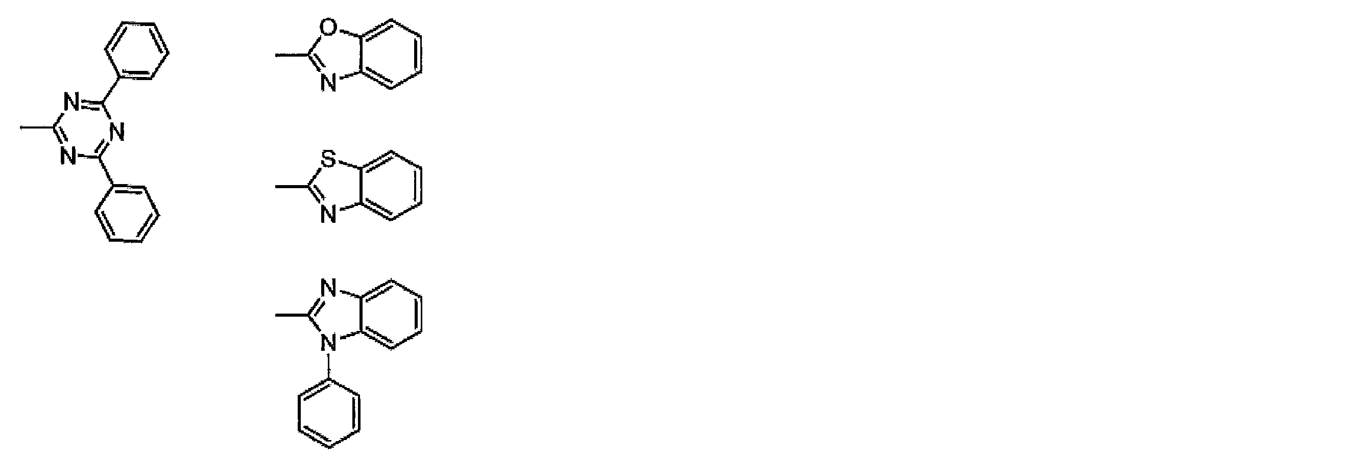
R12とR13が互いに結合して、R12とR13が結合しているベンゼン環とともに下記のいずれかの構造を形成している基(ただし水素原子は置換基で置換されていてもよい)である。

<2> R17がシアノ基または下記構造の基(ただし水素原子は置換基で置換されていてもよい)であるか、

R18がシアノ基または下記の群のいずれかの構造の基(ただし水素原子は置換基で置換されていてもよい)であるか、あるいは

R17とR18が互いに結合して、R17とR18が結合しているベンゼン環とともに下記のいずれかの構造を形成している基(ただし水素原子は置換基で置換されていてもよい)である。

]
[5] 一般式(3)のR1~R8が、各々独立に水素原子、炭素数1~10の置換もしくは無置換のアルキル基、炭素数1~10の置換もしくは無置換のアルコキシ基、炭素数6~15の置換もしくは無置換のアリール基、または炭素数3~12の置換もしくは無置換のヘテロアリール基であることを特徴とする[4]に記載の化合物。
[6] 一般式(3)のR12、R13、R17、R18のうちの少なくとも2つが上記<1>および<2>の条件を満たすように置換基を有しており、それ以外のR11~R20が各々独立に水素原子、フッ素原子、塩素原子、シアノ基、炭素数1~10の置換もしくは無置換のアルキル基、炭素数1~10の置換もしくは無置換のアルコキシ基、炭素数1~10の置換もしくは無置換のジアルキルアミノ基、炭素数12~40の置換もしくは無置換のジアリールアミノ基、炭素数6~15の置換もしくは無置換のアリール基、または炭素数3~12の置換もしくは無置換のヘテロアリール基であることを特徴とする[4]または[5]に記載の化合物。
[7] 一般式(3)の上記<1>および<2>中に記載される構造の水素原子が置換されていてもよい置換基が、フッ素原子、塩素原子、シアノ基、炭素数1~10の置換もしくは無置換のアルキル基、炭素数1~10の置換もしくは無置換のアルコキシ基、炭素数1~10の置換もしくは無置換のジアルキルアミノ基、炭素数12~40の置換もしくは無置換のジアリールアミノ基、炭素数6~15の置換もしくは無置換のアリール基、および炭素数3~12の置換もしくは無置換のヘテロアリール基からなる群より選択されることを特徴とする[4]~[6]のいずれか1項に記載の化合物。
<1> R12がシアノ基または下記構造の基(ただし水素原子は置換基で置換されていてもよい)であるか、
[5] 一般式(3)のR1~R8が、各々独立に水素原子、炭素数1~10の置換もしくは無置換のアルキル基、炭素数1~10の置換もしくは無置換のアルコキシ基、炭素数6~15の置換もしくは無置換のアリール基、または炭素数3~12の置換もしくは無置換のヘテロアリール基であることを特徴とする[4]に記載の化合物。
[6] 一般式(3)のR12、R13、R17、R18のうちの少なくとも2つが上記<1>および<2>の条件を満たすように置換基を有しており、それ以外のR11~R20が各々独立に水素原子、フッ素原子、塩素原子、シアノ基、炭素数1~10の置換もしくは無置換のアルキル基、炭素数1~10の置換もしくは無置換のアルコキシ基、炭素数1~10の置換もしくは無置換のジアルキルアミノ基、炭素数12~40の置換もしくは無置換のジアリールアミノ基、炭素数6~15の置換もしくは無置換のアリール基、または炭素数3~12の置換もしくは無置換のヘテロアリール基であることを特徴とする[4]または[5]に記載の化合物。
[7] 一般式(3)の上記<1>および<2>中に記載される構造の水素原子が置換されていてもよい置換基が、フッ素原子、塩素原子、シアノ基、炭素数1~10の置換もしくは無置換のアルキル基、炭素数1~10の置換もしくは無置換のアルコキシ基、炭素数1~10の置換もしくは無置換のジアルキルアミノ基、炭素数12~40の置換もしくは無置換のジアリールアミノ基、炭素数6~15の置換もしくは無置換のアリール基、および炭素数3~12の置換もしくは無置換のヘテロアリール基からなる群より選択されることを特徴とする[4]~[6]のいずれか1項に記載の化合物。
[8] [1]~[7]のいずれか1項に記載の化合物からなる発光材料。
[9] 上記一般式(1)で表される構造を有する遅延蛍光体。
[10] [8]に記載の発光材料を含む発光層を基板上に有することを特徴とする有機発光素子。
[11] 遅延蛍光を放射することを特徴とする[10]に記載の有機発光素子。
[12] 有機エレクトロルミネッセンス素子であることを特徴とする[10]または[11]に記載の有機発光素子。
[9] 上記一般式(1)で表される構造を有する遅延蛍光体。
[10] [8]に記載の発光材料を含む発光層を基板上に有することを特徴とする有機発光素子。
[11] 遅延蛍光を放射することを特徴とする[10]に記載の有機発光素子。
[12] 有機エレクトロルミネッセンス素子であることを特徴とする[10]または[11]に記載の有機発光素子。
本発明の化合物は、発光材料として有用である。また、本発明の化合物の中には遅延蛍光を放射するものが含まれている。本発明の化合物を発光材料として用いた有機発光素子は、高い発光効率を実現しうる。
以下において、本発明の内容について詳細に説明する。以下に記載する構成要件の説明は、本発明の代表的な実施態様や具体例に基づいてなされることがあるが、本発明はそのような実施態様や具体例に限定されるものではない。なお、本明細書において「~」を用いて表される数値範囲は、「~」の前後に記載される数値を下限値および上限値として含む範囲を意味する。また、本発明に用いられる化合物の分子内に存在する水素原子の同位体種は特に限定されず、例えば分子内の水素原子がすべて1Hであってもよいし、一部または全部が2H(デューテリウムD)であってもよい。
[一般式(1)で表される化合物]
本発明の化合物は、下記一般式(1)で表される構造を有することを特徴とする。
一般式(1)
A-D-A
本発明の化合物は、下記一般式(1)で表される構造を有することを特徴とする。
一般式(1)
A-D-A
一般式(1)において、Dは下記式で表される構造を含む2価の基を表す。

上記構造中に存在する水素原子は置換基で置換されていてもよい。置換基の数は特に制限されず、置換基は存在していなくてもよい。また、2つ以上の置換基が存在するときは、それらの置換基は互いに同一であっても異なっていてもよい。
置換基としては、例えばヒドロキシ基、ハロゲン原子、炭素数1~20のアルキル基、炭素数1~20のアルコキシ基、炭素数1~20のアルキルチオ基、炭素数6~40のアリール基、炭素数3~40のヘテロアリール基、炭素数2~10のアルケニル基、炭素数2~10のアルキニル基、炭素数1~10のハロアルキル基、炭素数3~20のトリアルキルシリル基、炭素数4~20のトリアルキルシリルアルキル基、炭素数5~20のトリアルキルシリルアルケニル基、炭素数5~20のトリアルキルシリルアルキニル基等が挙げられる。これらの具体例のうち、さらに置換基により置換可能なものは置換されていてもよい。より好ましい置換基は、炭素数1~20の置換もしくは無置換のアルキル基、炭素数1~20のアルコキシ基、炭素数6~40の置換もしくは無置換のアリール基、炭素数3~40の置換もしくは無置換のヘテロアリール基である。さらに好ましい置換基は、炭素数1~10の置換もしくは無置換のアルキル基、炭素数1~10の置換もしくは無置換のアルコキシ基、炭素数6~15の置換もしくは無置換のアリール基、炭素数3~12の置換もしくは無置換のヘテロアリール基である。
アルキル基は、直鎖状、分枝状、環状のいずれであってもよく、より好ましくは炭素数1~6であり、具体例としてメチル基、エチル基、プロピル基、ブチル基、tert-ブチル基、ペンチル基、ヘキシル基、イソプロピル基を挙げることができる。アルコキシ基は、直鎖状、分枝状、環状のいずれであってもよく、より好ましくは炭素数1~6であり、具体例としてメトキシ基、エトキシ基、プロポキシ基、ブトキシ基、tert-ブトキシ基、ペンチルオキシ基、ヘキシルオキシ基、イソプロピポキシ基を挙げることができる。置換基として採用しうるアリール基は、単環でも縮合環でもよく、具体例としてフェニル基、ナフチル基を挙げることができる。ヘテロアリール基も、単環でも縮合環でもよく、具体例としてピリジル基、ピリダジル基、ピリミジル基、トリアジル基、トリアゾリル基、ベンゾトリアゾリル基を挙げることができる。これらのヘテロアリール基は、ヘテロ原子を介して結合する基であっても、ヘテロアリール環を構成する炭素原子を介して結合する基であってもよい。
一般式(1)におけるDは、下記の一般式(2)で表される構造を有する基であることが好ましい。

一般式(2)において、R1~R8は各々独立に水素原子または置換基を表す。R1~R8はすべてが水素原子であってもよい。また、2個以上が置換基である場合、それらの置換基は同じであっても異なっていてもよい。R1~R8がとりうる置換基の説明と好ましい範囲については、上記の一般式(1)におけるDがとりうる置換基の説明と好ましい範囲を参照することができる。
R1とR2、R2とR3、R3とR4、R5とR6、R6とR7、R7とR8は互いに結合して環状構造を形成していてもよい。環状構造は芳香環であっても脂肪環であってもよく、またヘテロ原子を含むものであってもよく、さらに環状構造は2環以上の縮合環であってもよい。ここでいうヘテロ原子としては、窒素原子、酸素原子および硫黄原子からなる群より選択されるものであることが好ましい。形成される環状構造の例として、ベンゼン環、ナフタレン環、ピリジン環、ピリダジン環、ピリミジン環、ピラジン環、ピロール環、イミダゾール環、ピラゾール環、トリアゾール環、イミダゾリン環、オキサゾール環、イソオキサゾール環、チアゾール環、イソチアゾール環、シクロヘキサジエン環、シクロヘキセン環、シクロペンタエン環、シクロヘプタトリエン環、シクロヘプタジエン環、シクロヘプタエン環などを挙げることができる。
一般式(2)で表される構造の好ましい例として、R1~R8がすべて水素原子である構造を挙げることができる。また、R1とR8、R2とR7、R3とR6、R4とR5がそれぞれ同一である線対称の構造や、R1とR5、R2とR6、R3とR7、R4とR8がそれぞれ同一である回転対称の構造も挙げることができる。
一般式(1)において、Aは下記の群から選択される構造の基を表す。

上の群に記載される構造中に存在する各水素原子は置換基で置換されていてもよい。置換基の数は特に制限されず、置換基は存在していなくてもよい。また、2つ以上の置換基が存在するときは、それらの置換基は互いに同一であっても異なっていてもよい。
上の群に記載される構造中に存在する水素原子が置換されうる置換基としては、例えばヒドロキシ基、ハロゲン原子、シアノ基、炭素数1~20のアルキル基、炭素数1~20のアルコキシ基、炭素数1~20のアルキルチオ基、炭素数1~20のアルキル置換アミノ基、炭素数12~40のアリール置換アミノ基、炭素数2~20のアシル基、炭素数6~40のアリール基、炭素数3~40のヘテロアリール基、炭素数12~40の置換もしくは無置換のカルバゾリル基、炭素数2~10のアルケニル基、炭素数2~10のアルキニル基、炭素数2~10のアルコキシカルボニル基、炭素数1~10のアルキルスルホニル基、炭素数1~10のハロアルキル基、アミド基、炭素数2~10のアルキルアミド基、炭素数3~20のトリアルキルシリル基、炭素数4~20のトリアルキルシリルアルキル基、炭素数5~20のトリアルキルシリルアルケニル基、炭素数5~20のトリアルキルシリルアルキニル基およびニトロ基等が挙げられる。これらの具体例のうち、さらに置換基により置換可能なものは置換されていてもよい。より好ましい置換基は、ハロゲン原子、シアノ基、炭素数1~20の置換もしくは無置換のアルキル基、炭素数1~20のアルコキシ基、炭素数6~40の置換もしくは無置換のアリール基、炭素数3~40の置換もしくは無置換のヘテロアリール基、炭素数1~10の置換もしくは無置換のジアルキルアミノ基、炭素数12~40の置換もしくは無置換のジアリールアミノ基、炭素数12~40の置換もしくは無置換のカルバゾリル基である。さらに好ましい置換基は、フッ素原子、塩素原子、シアノ基、炭素数1~10の置換もしくは無置換のアルキル基、炭素数1~10の置換もしくは無置換のアルコキシ基、炭素数1~10の置換もしくは無置換のジアルキルアミノ基、炭素数12~40の置換もしくは無置換のジアリールアミノ基、炭素数6~15の置換もしくは無置換のアリール基、炭素数3~12の置換もしくは無置換のヘテロアリール基である。
上の群に記載される構造中に存在する隣合う環骨格原子に結合している水素原子同士は、互いに置換基が結合して環状構造を形成していてもよい。環状構造は芳香環であっても脂肪環であってもよく、またヘテロ原子を含むものであってもよく、さらに環状構造は2環以上の縮合環であってもよい。具体例については、上記の一般式(2)における環状構造の具体例を参照することができる。
上の群に記載される構造のうち好ましいのは、

のいずれかの構造であり、さらに好ましくは

のいずれかの構造である。
一般式(1)における2つのAは、互いに同一であっても異なっていてもよいが、同一であることが好ましい。2つのAが互いに同一であるときは、分子全体が線対称または点対称となっていることが好ましい。
通常の発光材料はアクセプターとして作用するAとドナーとして作用するDが結合したA-D構造を有する。これに対して一般式(1)で表される化合物は、A-D-Aの構造を有しており、ドナーとして作用するDに対してアクセプターとして作用するAが2つ結合している。Aが2つ以上結合しているとアクセプターとしての機能が打ち消しあって、分子が発光材料として有効に機能しない危険性が生じることが一般に懸念される。しかしながら、本発明にしたがってAとDをそれぞれ選りすぐって互いに組み合わせることにより、発光効率が高くて優れた効果を有する発光材料を提供できることが判明した。これは、HOMOとLUMOの広がりを分子レベルで制御して、発光材料として好ましい条件を満たすようにしたためであると考えられる。
一般式(1)で表される化合物は、下記一般式(3)で表される構造を有する化合物であることが好ましい。
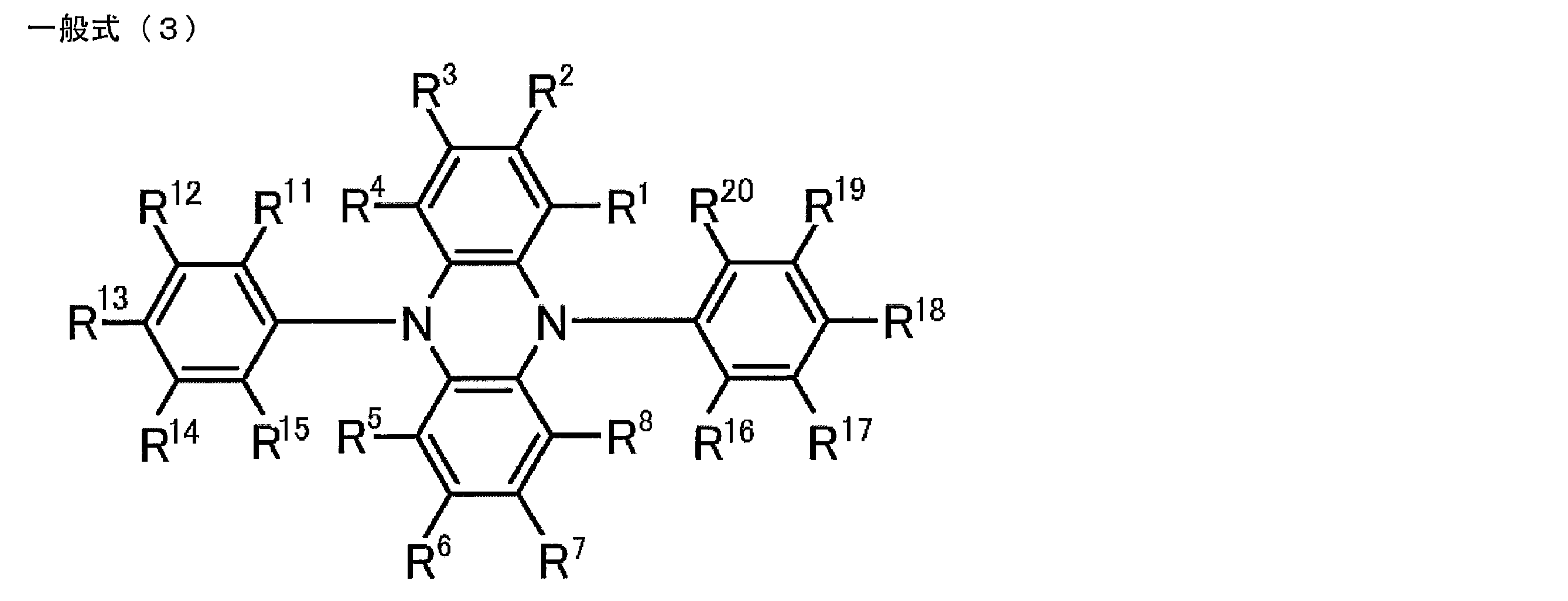
一般式(3)において、R1~R8およびR11~R20は各々独立に水素原子または置換基を表す。R1とR2、R2とR3、R3とR4、R5とR6、R6とR7、R7とR8、R11とR12、R12とR13、R13とR14、R14とR15、R16とR17、R17とR18、R18とR19、R19とR20は互いに結合して環状構造を形成していてもよい。R1~R8がとりうる置換基の説明と好ましい範囲については、一般式(1)の対応する記載を参照することができる。R11~R20がとりうる置換基の説明と好ましい範囲については、一般式(1)のAに存在しうる置換基の記載を参照することができる。なお一般式(3)は、以下の<1>および<2>の条件を満たす。
<1> R12がシアノ基または下記構造の基(ただし水素原子は置換基で置換されていてもよい)であるか、

R13がシアノ基または下記の群のいずれかの構造の基(ただし水素原子は置換基で置換されていてもよい)であるか、あるいは

R12とR13が互いに結合して、R12とR13が結合しているベンゼン環とともに下記のいずれかの構造を形成している基(ただし水素原子は置換基で置換されていてもよい)である。

<2> R17がシアノ基または下記構造の基(ただし水素原子は置換基で置換されていてもよい)であるか、

R18がシアノ基または下記の群のいずれかの構造の基(ただし水素原子は置換基で置換されていてもよい)であるか、あるいは

R17とR18が互いに結合して、R17とR18が結合しているベンゼン環とともに下記のいずれかの構造を形成している基(ただし水素原子は置換基で置換されていてもよい)である。

<1> R12がシアノ基または下記構造の基(ただし水素原子は置換基で置換されていてもよい)であるか、
上記<1>および<2>の中に記載されている構造の説明については、一般式(1)のAの構造の対応する記載を参照することができる。
一般式(3)のR1~R8は、各々独立に水素原子、炭素数1~10の置換もしくは無置換のアルキル基、炭素数1~10の置換もしくは無置換のアルコキシ基、炭素数6~15の置換もしくは無置換のアリール基、炭素数3~12の置換もしくは無置換のヘテロアリール基であることが好ましい。
また、一般式(3)のR12、R13、R17、R18のうちの少なくとも2つが上記<1>および<2>の条件を満たすように置換基を有しており、それ以外のR11~R18が各々独立に水素原子、フッ素原子、塩素原子、シアノ基、炭素数1~10の置換もしくは無置換のアルキル基、炭素数1~10の置換もしくは無置換のアルコキシ基、炭素数1~10の置換もしくは無置換のジアルキルアミノ基、炭素数12~40の置換もしくは無置換のジアリールアミノ基、炭素数6~15の置換もしくは無置換のアリール基、または炭素数3~12の置換もしくは無置換のヘテロアリール基であることが好ましい。
さらに一般式(3)の上記<1>および<2>中に記載される構造の水素原子が置換されていてもよい置換基が、フッ素原子、塩素原子、シアノ基、炭素数1~10の置換もしくは無置換のアルキル基、炭素数1~10の置換もしくは無置換のアルコキシ基、炭素数1~10の置換もしくは無置換のジアルキルアミノ基、炭素数12~40の置換もしくは無置換のジアリールアミノ基、炭素数6~15の置換もしくは無置換のアリール基、および炭素数3~12の置換もしくは無置換のヘテロアリール基からなる群より選択されることが好ましい。
以下において、一般式(1)で表される化合物の具体例を例示する。ただし、本発明において用いることができる一般式(1)で表される化合物はこれらの具体例によって限定的に解釈されるべきものではない。


一般式(1)で表される化合物の分子量は、例えば一般式(1)で表される化合物を含む有機層を蒸着法により製膜して利用することを意図する場合には、1500以下であることが好ましく、1200以下であることがより好ましく、1000以下であることがさらに好ましく、800以下であることがさらにより好ましい。分子量の下限値は、一般式(1)で表される最小化合物の分子量である。
一般式(1)で表される化合物は、分子量にかかわらず塗布法で成膜してもよい。塗布法を用いれば、分子量が比較的大きな化合物であっても成膜することが可能である。
一般式(1)で表される化合物は、分子量にかかわらず塗布法で成膜してもよい。塗布法を用いれば、分子量が比較的大きな化合物であっても成膜することが可能である。
本発明を応用して、分子内に一般式(1)で表される構造を複数個含む化合物を、発光材料として用いることも考えられる。
例えば、一般式(1)で表される構造中にあらかじめ重合性基を存在させておいて、その重合性基を重合させることによって得られる重合体を、発光材料として用いることが考えられる。具体的には、一般式(1)のAかDのいずれかに重合性官能基を含むモノマーを用意して、これを単独で重合させるか、他のモノマーとともに共重合させることにより、繰り返し単位を有する重合体を得て、その重合体を発光材料として用いることが考えられる。あるいは、一般式(1)で表される構造を有する化合物どうしを反応させることにより、二量体や三量体を得て、それらを発光材料として用いることも考えられる。
例えば、一般式(1)で表される構造中にあらかじめ重合性基を存在させておいて、その重合性基を重合させることによって得られる重合体を、発光材料として用いることが考えられる。具体的には、一般式(1)のAかDのいずれかに重合性官能基を含むモノマーを用意して、これを単独で重合させるか、他のモノマーとともに共重合させることにより、繰り返し単位を有する重合体を得て、その重合体を発光材料として用いることが考えられる。あるいは、一般式(1)で表される構造を有する化合物どうしを反応させることにより、二量体や三量体を得て、それらを発光材料として用いることも考えられる。
一般式(1)で表される構造を含む繰り返し単位を有する重合体の例として、下記一般式(4)または(5)で表される構造を含む重合体を挙げることができる。

一般式(4)および(5)において、Qは一般式(1)で表される構造を含む基を表し、L1およびL2は連結基を表す。連結基の炭素数は、好ましくは0~20であり、より好ましくは1~15であり、さらに好ましくは2~10である。連結基は-X11-L11-で表される構造を有するものであることが好ましい。ここで、X11は酸素原子または硫黄原子を表し、酸素原子であることが好ましい。L11は連結基を表し、置換もしくは無置換のアルキレン基、または置換もしくは無置換のアリーレン基であることが好ましく、炭素数1~10の置換もしくは無置換のアルキレン基、または置換もしくは無置換のフェニレン基であることがより好ましい。
一般式(4)および(5)において、R101、R102、R103およびR104は、各々独立に置換基を表す。好ましくは、炭素数1~6の置換もしくは無置換のアルキル基、炭素数1~6の置換もしくは無置換のアルコキシ基、ハロゲン原子であり、より好ましくは炭素数1~3の無置換のアルキル基、炭素数1~3の無置換のアルコキシ基、フッ素原子、塩素原子であり、さらに好ましくは炭素数1~3の無置換のアルキル基、炭素数1~3の無置換のアルコキシ基である。
L1およびL2で表される連結基は、Qを構成する一般式(1)の構造のAかD、一般式(3)の構造のR1~R8、R11~R18のいずれかに結合することができる。1つのQに対して連結基が2つ以上連結して架橋構造や網目構造を形成していてもよい。
繰り返し単位の具体的な構造例として、下記式(6)~(9)で表される構造を挙げることができる。
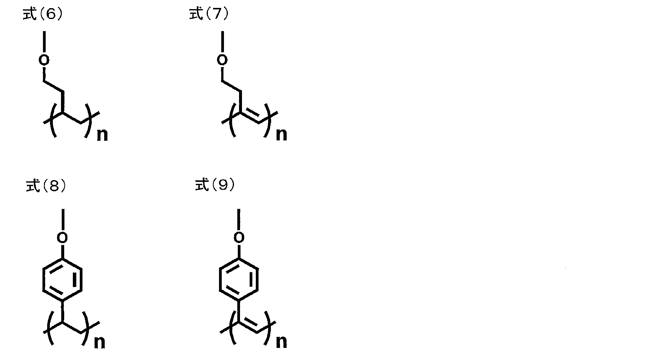
これらの式(6)~(9)を含む繰り返し単位を有する重合体は、一般式(1)の構造のAかDのいずれかにヒドロキシ基を導入しておき、それをリンカーとして下記化合物を反応させて重合性基を導入し、その重合性基を重合させることにより合成することができる。
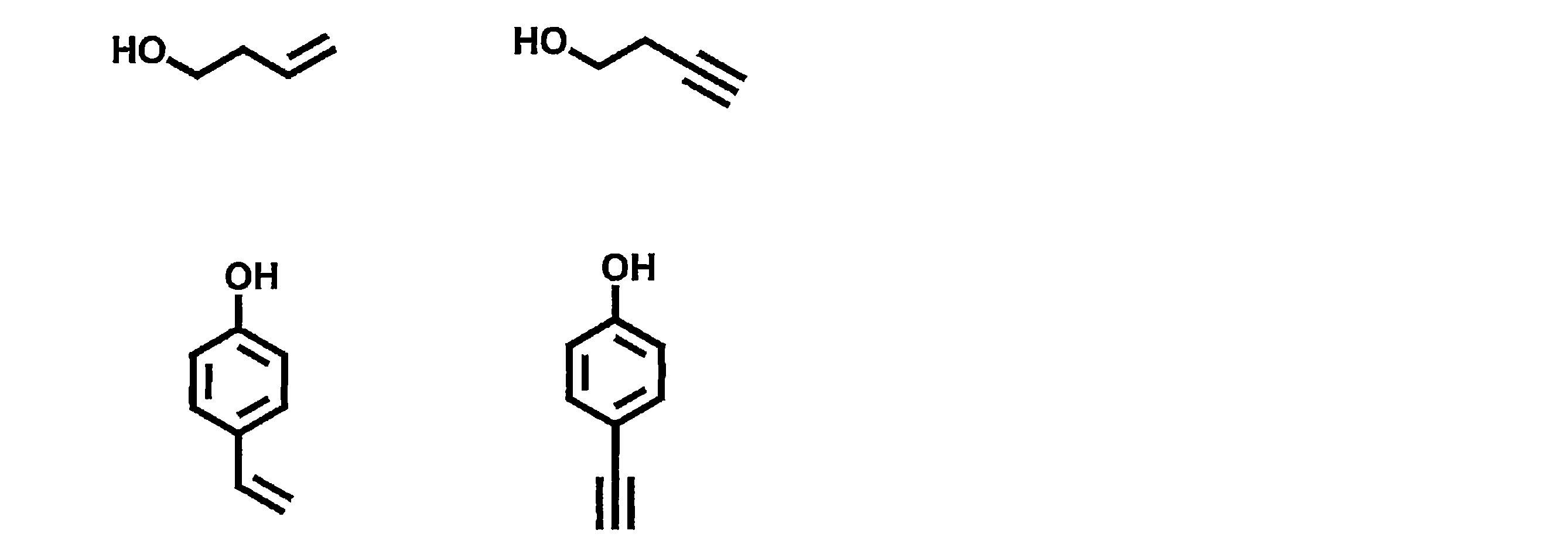
分子内に一般式(1)で表される構造を含む重合体は、一般式(1)で表される構造を有する繰り返し単位のみからなる重合体であってもよいし、それ以外の構造を有する繰り返し単位を含む重合体であってもよい。また、重合体の中に含まれる一般式(1)で表される構造を有する繰り返し単位は、単一種であってもよいし、2種以上であってもよい。一般式(1)で表される構造を有さない繰り返し単位としては、通常の共重合に用いられるモノマーから誘導されるものを挙げることができる。例えば、エチレン、スチレンなどのエチレン性不飽和結合を有するモノマーから誘導される繰り返し単位を挙げることができる。
[一般式(1)で表される化合物の合成方法]
一般式(1)で表される化合物は、既知の反応を組み合わせることによって合成することができる。例えば、以下のスキームにしたがって合成することが可能である。

上式におけるDおよびAの説明については、一般式(1)における対応する記載を参照することができる。上式におけるXはハロゲン原子を表し、フッ素原子、塩素原子、臭素原子、ヨウ素原子を挙げることができ、塩素原子、臭素原子、ヨウ素原子が好ましい。
一般式(1)で表される化合物のうち、例えば一般式(3)で表される化合物は以下のスキームにより合成することが可能である。ただし、以下に記載するスキームは、R11とR16、R12とR17、R13とR18、R14とR19、R15とR20が同一である場合の合成法を示すものである。
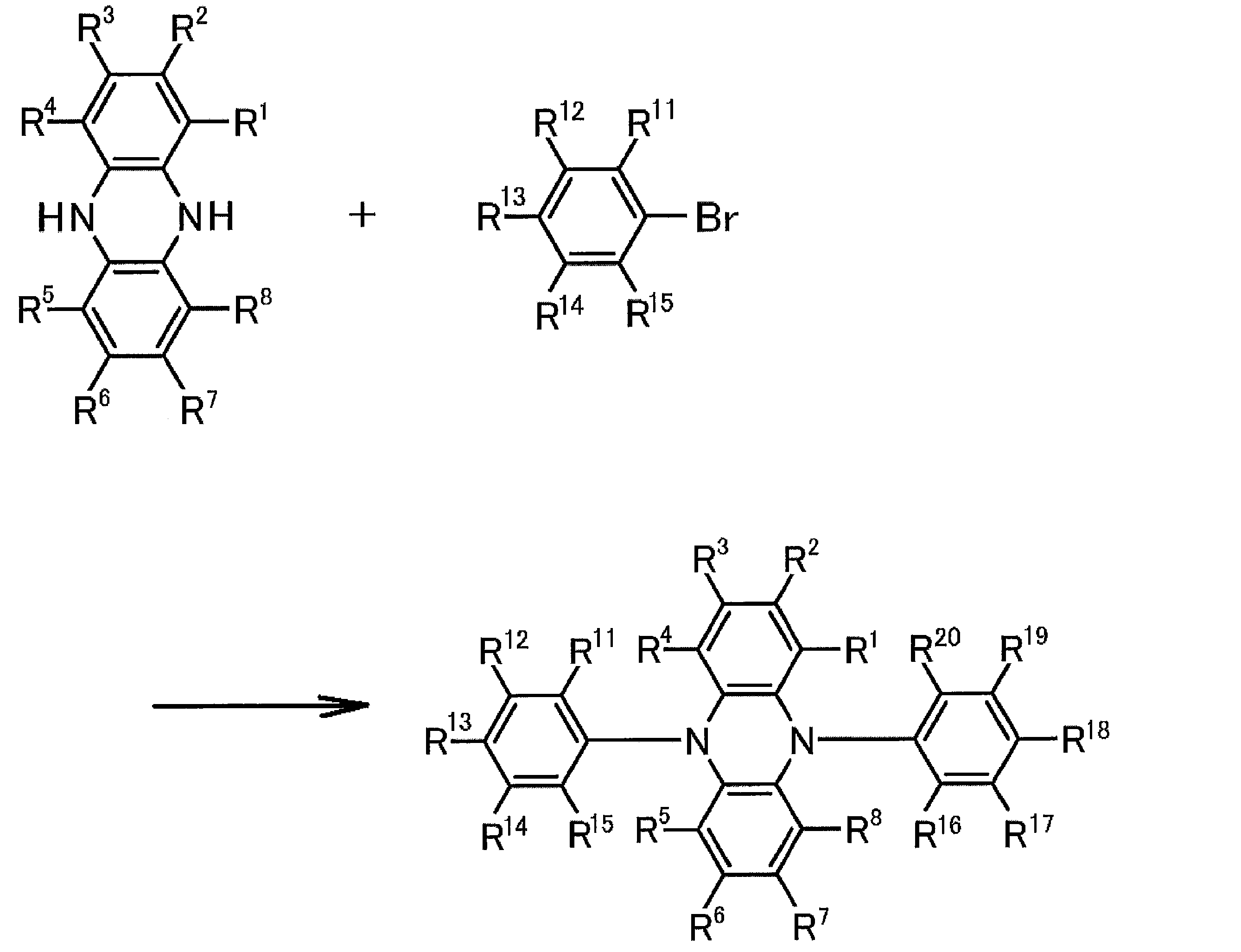
一般式(1)で表される化合物は、既知の反応を組み合わせることによって合成することができる。例えば、以下のスキームにしたがって合成することが可能である。
一般式(1)で表される化合物のうち、例えば一般式(3)で表される化合物は以下のスキームにより合成することが可能である。ただし、以下に記載するスキームは、R11とR16、R12とR17、R13とR18、R14とR19、R15とR20が同一である場合の合成法を示すものである。
上式におけるR1~R8およびR11~R20の説明については、一般式(3)における対応する記載を参照することができる。上式におけるXはハロゲン原子を表す。
上記の2つのスキームにおける反応は、公知の反応を応用したものであり、公知の反応条件を適宜選択して用いることができる。上記の反応の詳細については、後述の合成例を参考にすることができる。また、一般式(1)で表される化合物は、その他の公知の合成反応を組み合わせることによっても合成することができる。
上記の2つのスキームにおける反応は、公知の反応を応用したものであり、公知の反応条件を適宜選択して用いることができる。上記の反応の詳細については、後述の合成例を参考にすることができる。また、一般式(1)で表される化合物は、その他の公知の合成反応を組み合わせることによっても合成することができる。
[有機発光素子]
本発明の一般式(1)で表される化合物は、有機発光素子の発光材料として有用である。このため、本発明の一般式(1)で表される化合物は、有機発光素子の発光層に発光材料として効果的に用いることができる。一般式(1)で表される化合物の中には、遅延蛍光を放射する遅延蛍光材料(遅延蛍光体)が含まれている。すなわち本発明は、一般式(1)で表される構造を有する遅延蛍光体の発明と、一般式(1)で表される化合物を遅延蛍光体として使用する発明と、一般式(1)で表される化合物を用いて遅延蛍光を発光させる方法の発明も提供する。そのような化合物を発光材料として用いた有機発光素子は、遅延蛍光を放射し、発光効率が高いという特徴を有する。その原理を、有機エレクトロルミネッセンス素子を例にとって説明すると以下のようになる。
本発明の一般式(1)で表される化合物は、有機発光素子の発光材料として有用である。このため、本発明の一般式(1)で表される化合物は、有機発光素子の発光層に発光材料として効果的に用いることができる。一般式(1)で表される化合物の中には、遅延蛍光を放射する遅延蛍光材料(遅延蛍光体)が含まれている。すなわち本発明は、一般式(1)で表される構造を有する遅延蛍光体の発明と、一般式(1)で表される化合物を遅延蛍光体として使用する発明と、一般式(1)で表される化合物を用いて遅延蛍光を発光させる方法の発明も提供する。そのような化合物を発光材料として用いた有機発光素子は、遅延蛍光を放射し、発光効率が高いという特徴を有する。その原理を、有機エレクトロルミネッセンス素子を例にとって説明すると以下のようになる。
有機エレクトロルミネッセンス素子においては、正負の両電極より発光材料にキャリアを注入し、励起状態の発光材料を生成し、発光させる。通常、キャリア注入型の有機エレクトロルミネッセンス素子の場合、生成した励起子のうち、励起一重項状態に励起されるのは25%であり、残り75%は励起三重項状態に励起される。従って、励起三重項状態からの発光であるリン光を利用するほうが、エネルギーの利用効率が高い。しかしながら、励起三重項状態は寿命が長いため、励起状態の飽和や励起三重項状態の励起子との相互作用によるエネルギーの失活が起こり、一般にリン光の量子収率が高くないことが多い。一方、遅延蛍光材料は、項間交差等により励起三重項状態へとエネルギーが遷移した後、三重項-三重項消滅あるいは熱エネルギーの吸収により、励起一重項状態に逆項間交差され蛍光を放射する。有機エレクトロルミネッセンス素子においては、なかでも熱エネルギーの吸収による熱活性化型の遅延蛍光材料が特に有用であると考えられる。有機エレクトロルミネッセンス素子に遅延蛍光材料を利用した場合、励起一重項状態の励起子は通常通り蛍光を放射する。一方、励起三重項状態の励起子は、デバイスが発する熱を吸収して励起一重項へ項間交差され蛍光を放射する。このとき、励起一重項からの発光であるため蛍光と同波長での発光でありながら、励起三重項状態から励起一重項状態への逆項間交差により、生じる光の寿命(発光寿命)は通常の蛍光やりん光よりも長くなるため、これらよりも遅延した蛍光として観察される。これを遅延蛍光として定義できる。このような熱活性化型の励起子移動機構を用いれば、キャリア注入後に熱エネルギーの吸収を経ることにより、通常は25%しか生成しなかった励起一重項状態の化合物の比率を25%以上に引き上げることが可能となる。100℃未満の低い温度でも強い蛍光および遅延蛍光を発する化合物を用いれば、デバイスの熱で充分に励起三重項状態から励起一重項状態への項間交差が生じて遅延蛍光を放射するため、発光効率を飛躍的に向上させることができる。
本発明の一般式(1)で表される化合物を発光層の発光材料として用いることにより、有機フォトルミネッセンス素子(有機PL素子)や有機エレクトロルミネッセンス素子(有機EL素子)などの優れた有機発光素子を提供することができる。このとき、本発明の一般式(1)で表される化合物は、いわゆるアシストドーパントとして、発光層に含まれる他の発光材料の発光をアシストする機能を有するものであってもよい。すなわち、発光層に含まれる本発明の一般式(1)で表される化合物は、発光層に含まれるホスト材料の最低励起一重項エネルギー準位と発光層に含まれる他の発光材料の最低励起一重項エネルギー準位の間の最低励起一重項エネルギー準位を有するものであってもよい。
有機フォトルミネッセンス素子は、基板上に少なくとも発光層を形成した構造を有する。また、有機エレクトロルミネッセンス素子は、少なくとも陽極、陰極、および陽極と陰極の間に有機層を形成した構造を有する。有機層は、少なくとも発光層を含むものであり、発光層のみからなるものであってもよいし、発光層の他に1層以上の有機層を有するものであってもよい。そのような他の有機層として、正孔輸送層、正孔注入層、電子阻止層、正孔阻止層、電子注入層、電子輸送層、励起子阻止層などを挙げることができる。正孔輸送層は正孔注入機能を有した正孔注入輸送層でもよく、電子輸送層は電子注入機能を有した電子注入輸送層でもよい。具体的な有機エレクトロルミネッセンス素子の構造例を図1に示す。図1において、1は基板、2は陽極、3は正孔注入層、4は正孔輸送層、5は発光層、6は電子輸送層、7は陰極を表わす。
以下において、有機エレクトロルミネッセンス素子の各部材および各層について説明する。なお、基板と発光層の説明は有機フォトルミネッセンス素子の基板と発光層にも該当する。
(基板)
本発明の有機エレクトロルミネッセンス素子は、基板に支持されていることが好ましい。この基板については、特に制限はなく、従来から有機エレクトロルミネッセンス素子に慣用されているものであればよく、例えば、ガラス、透明プラスチック、石英、シリコンなどからなるものを用いることができる。
本発明の有機エレクトロルミネッセンス素子は、基板に支持されていることが好ましい。この基板については、特に制限はなく、従来から有機エレクトロルミネッセンス素子に慣用されているものであればよく、例えば、ガラス、透明プラスチック、石英、シリコンなどからなるものを用いることができる。
(陽極)
有機エレクトロルミネッセンス素子における陽極としては、仕事関数の大きい(4eV以上)金属、合金、電気伝導性化合物およびこれらの混合物を電極材料とするものが好ましく用いられる。このような電極材料の具体例としてはAu等の金属、CuI、インジウムチンオキシド(ITO)、SnO2、ZnO等の導電性透明材料が挙げられる。また、IDIXO(In2O3-ZnO)等非晶質で透明導電膜を作製可能な材料を用いてもよい。陽極はこれらの電極材料を蒸着やスパッタリング等の方法により、薄膜を形成させ、フォトリソグラフィー法で所望の形状のパターンを形成してもよく、あるいはパターン精度をあまり必要としない場合は(100μm以上程度)、上記電極材料の蒸着やスパッタリング時に所望の形状のマスクを介してパターンを形成してもよい。あるいは、有機導電性化合物のように塗布可能な材料を用いる場合には、印刷方式、コーティング方式等湿式成膜法を用いることもできる。この陽極より発光を取り出す場合には、透過率を10%より大きくすることが望ましく、また陽極としてのシート抵抗は数百Ω/□以下が好ましい。さらに膜厚は材料にもよるが、通常10~1000nm、好ましくは10~200nmの範囲で選ばれる。
有機エレクトロルミネッセンス素子における陽極としては、仕事関数の大きい(4eV以上)金属、合金、電気伝導性化合物およびこれらの混合物を電極材料とするものが好ましく用いられる。このような電極材料の具体例としてはAu等の金属、CuI、インジウムチンオキシド(ITO)、SnO2、ZnO等の導電性透明材料が挙げられる。また、IDIXO(In2O3-ZnO)等非晶質で透明導電膜を作製可能な材料を用いてもよい。陽極はこれらの電極材料を蒸着やスパッタリング等の方法により、薄膜を形成させ、フォトリソグラフィー法で所望の形状のパターンを形成してもよく、あるいはパターン精度をあまり必要としない場合は(100μm以上程度)、上記電極材料の蒸着やスパッタリング時に所望の形状のマスクを介してパターンを形成してもよい。あるいは、有機導電性化合物のように塗布可能な材料を用いる場合には、印刷方式、コーティング方式等湿式成膜法を用いることもできる。この陽極より発光を取り出す場合には、透過率を10%より大きくすることが望ましく、また陽極としてのシート抵抗は数百Ω/□以下が好ましい。さらに膜厚は材料にもよるが、通常10~1000nm、好ましくは10~200nmの範囲で選ばれる。
(陰極)
一方、陰極としては、仕事関数の小さい(4eV以下)金属(電子注入性金属と称する)、合金、電気伝導性化合物およびこれらの混合物を電極材料とするものが用いられる。このような電極材料の具体例としては、ナトリウム、ナトリウム-カリウム合金、マグネシウム、リチウム、マグネシウム/銅混合物、マグネシウム/銀混合物、マグネシウム/アルミニウム混合物、マグネシウム/インジウム混合物、アルミニウム/酸化アルミニウム(Al2O3)混合物、インジウム、リチウム/アルミニウム混合物、希土類金属等が挙げられる。これらの中で、電子注入性および酸化等に対する耐久性の点から、電子注入性金属とこれより仕事関数の値が大きく安定な金属である第二金属との混合物、例えば、マグネシウム/銀混合物、マグネシウム/アルミニウム混合物、マグネシウム/インジウム混合物、アルミニウム/酸化アルミニウム(Al2O3)混合物、リチウム/アルミニウム混合物、アルミニウム等が好適である。陰極はこれらの電極材料を蒸着やスパッタリング等の方法により薄膜を形成させることにより、作製することができる。また、陰極としてのシート抵抗は数百Ω/□以下が好ましく、膜厚は通常10nm~5μm、好ましくは50~200nmの範囲で選ばれる。なお、発光した光を透過させるため、有機エレクトロルミネッセンス素子の陽極または陰極のいずれか一方が、透明または半透明であれば発光輝度が向上し好都合である。
また、陽極の説明で挙げた導電性透明材料を陰極に用いることで、透明または半透明の陰極を作製することができ、これを応用することで陽極と陰極の両方が透過性を有する素子を作製することができる。
(発光層)
発光層は、陽極および陰極のそれぞれから注入された正孔および電子が再結合することにより励起子が生成した後、発光する層であり、発光材料を単独で発光層に使用しても良いが、好ましくは発光材料とホスト材料を含む。発光材料としては、一般式(1)で表される本発明の化合物群から選ばれる1種または2種以上を用いることができる。本発明の有機エレクトロルミネッセンス素子および有機フォトルミネッセンス素子が高い発光効率を発現するためには、発光材料に生成した一重項励起子および三重項励起子を、発光材料中に閉じ込めることが重要である。従って、発光層中に発光材料に加えてホスト材料を用いることが好ましい。ホスト材料としては、励起一重項エネルギー、励起三重項エネルギーの少なくとも何れか一方が本発明の発光材料よりも高い値を有する有機化合物を用いることができる。その結果、本発明の発光材料に生成した一重項励起子および三重項励起子を、本発明の発光材料の分子中に閉じ込めることが可能となり、その発光効率を十分に引き出すことが可能となる。もっとも、一重項励起子および三重項励起子を十分に閉じ込めることができなくても、高い発光効率を得ることが可能な場合もあるため、高い発光効率を実現しうるホスト材料であれば特に制約なく本発明に用いることができる。本発明の有機発光素子または有機エレクトロルミネッセンス素子において、発光は発光層に含まれる本発明の発光材料から生じる。この発光は蛍光発光および遅延蛍光発光の両方を含む。但し、発光の一部には、ホスト材料からの発光が含まれていてもかまわない。
ホスト材料を用いる場合、発光材料である本発明の化合物が発光層中に含有される量は0.1重量%以上であることが好ましく、1重量%以上であることがより好ましく、また、50重量%以下であることが好ましく、20重量%以下であることがより好ましく、10重量%以下であることがさらに好ましい。
発光層におけるホスト材料としては、正孔輸送能、電子輸送能を有し、かつ発光の長波長化を防ぎ、なおかつ高いガラス転移温度を有する有機化合物であることが好ましい。
(注入層)
注入層とは、駆動電圧低下や発光輝度向上のために電極と有機層間に設けられる層のことで、正孔注入層と電子注入層があり、陽極と発光層または正孔輸送層の間、および陰極と発光層または電子輸送層との間に存在させてもよい。注入層は必要に応じて設けることができる。
注入層とは、駆動電圧低下や発光輝度向上のために電極と有機層間に設けられる層のことで、正孔注入層と電子注入層があり、陽極と発光層または正孔輸送層の間、および陰極と発光層または電子輸送層との間に存在させてもよい。注入層は必要に応じて設けることができる。
(阻止層)
阻止層は、発光層中に存在する電荷(電子もしくは正孔)および/または励起子の発光層外への拡散を阻止することができる層である。電子阻止層は、発光層および正孔輸送層の間に配置されることができ、電子が正孔輸送層の方に向かって発光層を通過することを阻止する。同様に、正孔阻止層は発光層および電子輸送層の間に配置されることができ、正孔が電子輸送層の方に向かって発光層を通過することを阻止する。阻止層はまた、励起子が発光層の外側に拡散することを阻止するために用いることができる。すなわち電子阻止層、正孔阻止層はそれぞれ励起子阻止層としての機能も兼ね備えることができる。本明細書でいう電子阻止層または励起子阻止層は、一つの層で電子阻止層および励起子阻止層の機能を有する層を含む意味で使用される。
阻止層は、発光層中に存在する電荷(電子もしくは正孔)および/または励起子の発光層外への拡散を阻止することができる層である。電子阻止層は、発光層および正孔輸送層の間に配置されることができ、電子が正孔輸送層の方に向かって発光層を通過することを阻止する。同様に、正孔阻止層は発光層および電子輸送層の間に配置されることができ、正孔が電子輸送層の方に向かって発光層を通過することを阻止する。阻止層はまた、励起子が発光層の外側に拡散することを阻止するために用いることができる。すなわち電子阻止層、正孔阻止層はそれぞれ励起子阻止層としての機能も兼ね備えることができる。本明細書でいう電子阻止層または励起子阻止層は、一つの層で電子阻止層および励起子阻止層の機能を有する層を含む意味で使用される。
(正孔阻止層)
正孔阻止層とは広い意味では電子輸送層の機能を有する。正孔阻止層は電子を輸送しつつ、正孔が電子輸送層へ到達することを阻止する役割があり、これにより発光層中での電子と正孔の再結合確率を向上させることができる。正孔阻止層の材料としては、後述する電子輸送層の材料を必要に応じて用いることができる。
正孔阻止層とは広い意味では電子輸送層の機能を有する。正孔阻止層は電子を輸送しつつ、正孔が電子輸送層へ到達することを阻止する役割があり、これにより発光層中での電子と正孔の再結合確率を向上させることができる。正孔阻止層の材料としては、後述する電子輸送層の材料を必要に応じて用いることができる。
(電子阻止層)
電子阻止層とは、広い意味では正孔を輸送する機能を有する。電子阻止層は正孔を輸送しつつ、電子が正孔輸送層へ到達することを阻止する役割があり、これにより発光層中での電子と正孔が再結合する確率を向上させることができる。
電子阻止層とは、広い意味では正孔を輸送する機能を有する。電子阻止層は正孔を輸送しつつ、電子が正孔輸送層へ到達することを阻止する役割があり、これにより発光層中での電子と正孔が再結合する確率を向上させることができる。
(励起子阻止層)
励起子阻止層とは、発光層内で正孔と電子が再結合することにより生じた励起子が電荷輸送層に拡散することを阻止するための層であり、本層の挿入により励起子を効率的に発光層内に閉じ込めることが可能となり、素子の発光効率を向上させることができる。励起子阻止層は発光層に隣接して陽極側、陰極側のいずれにも挿入することができ、両方同時に挿入することも可能である。すなわち、励起子阻止層を陽極側に有する場合、正孔輸送層と発光層の間に、発光層に隣接して該層を挿入することができ、陰極側に挿入する場合、発光層と陰極との間に、発光層に隣接して該層を挿入することができる。また、陽極と、発光層の陽極側に隣接する励起子阻止層との間には、正孔注入層や電子阻止層などを有することができ、陰極と、発光層の陰極側に隣接する励起子阻止層との間には、電子注入層、電子輸送層、正孔阻止層などを有することができる。阻止層を配置する場合、阻止層として用いる材料の励起一重項エネルギーおよび励起三重項エネルギーの少なくともいずれか一方は、発光材料の励起一重項エネルギーおよび励起三重項エネルギーよりも高いことが好ましい。
励起子阻止層とは、発光層内で正孔と電子が再結合することにより生じた励起子が電荷輸送層に拡散することを阻止するための層であり、本層の挿入により励起子を効率的に発光層内に閉じ込めることが可能となり、素子の発光効率を向上させることができる。励起子阻止層は発光層に隣接して陽極側、陰極側のいずれにも挿入することができ、両方同時に挿入することも可能である。すなわち、励起子阻止層を陽極側に有する場合、正孔輸送層と発光層の間に、発光層に隣接して該層を挿入することができ、陰極側に挿入する場合、発光層と陰極との間に、発光層に隣接して該層を挿入することができる。また、陽極と、発光層の陽極側に隣接する励起子阻止層との間には、正孔注入層や電子阻止層などを有することができ、陰極と、発光層の陰極側に隣接する励起子阻止層との間には、電子注入層、電子輸送層、正孔阻止層などを有することができる。阻止層を配置する場合、阻止層として用いる材料の励起一重項エネルギーおよび励起三重項エネルギーの少なくともいずれか一方は、発光材料の励起一重項エネルギーおよび励起三重項エネルギーよりも高いことが好ましい。
(正孔輸送層)
正孔輸送層とは正孔を輸送する機能を有する正孔輸送材料からなり、正孔輸送層は単層または複数層設けることができる。
正孔輸送材料としては、正孔の注入または輸送、電子の障壁性のいずれかを有するものであり、有機物、無機物のいずれであってもよい。使用できる公知の正孔輸送材料としては例えば、トリアゾール誘導体、オキサジアゾール誘導体、イミダゾール誘導体、カルバゾール誘導体、インドロカルバゾール誘導体、ポリアリールアルカン誘導体、ピラゾリン誘導体およびピラゾロン誘導体、フェニレンジアミン誘導体、アリールアミン誘導体、アミノ置換カルコン誘導体、オキサゾール誘導体、スチリルアントラセン誘導体、フルオレノン誘導体、ヒドラゾン誘導体、スチルベン誘導体、シラザン誘導体、アニリン系共重合体、また導電性高分子オリゴマー、特にチオフェンオリゴマー等が挙げられるが、ポルフィリン化合物、芳香族第3級アミン化合物およびスチリルアミン化合物を用いることが好ましく、芳香族第3級アミン化合物を用いることがより好ましい。
(電子輸送層)
電子輸送層とは電子を輸送する機能を有する材料からなり、電子輸送層は単層または複数層設けることができる。
電子輸送材料(正孔阻止材料を兼ねる場合もある)としては、陰極より注入された電子を発光層に伝達する機能を有していればよい。使用できる電子輸送層としては例えば、ニトロ置換フルオレン誘導体、ジフェニルキノン誘導体、チオピランジオキシド誘導体、カルボジイミド、フレオレニリデンメタン誘導体、アントラキノジメタンおよびアントロン誘導体、オキサジアゾール誘導体等が挙げられる。さらに、上記オキサジアゾール誘導体において、オキサジアゾール環の酸素原子を硫黄原子に置換したチアジアゾール誘導体、電子吸引基として知られているキノキサリン環を有するキノキサリン誘導体も、電子輸送材料として用いることができる。さらにこれらの材料を高分子鎖に導入した、またはこれらの材料を高分子の主鎖とした高分子材料を用いることもできる。
有機エレクトロルミネッセンス素子を作製する際には、一般式(1)で表される化合物を発光層に用いるだけでなく、発光層以外の層にも用いてもよい。その際、発光層に用いる一般式(1)で表される化合物と、発光層以外の層に用いる一般式(1)で表される化合物は、同一であっても異なっていてもよい。例えば、上記の注入層、阻止層、正孔阻止層、電子阻止層、励起子阻止層、正孔輸送層、電子輸送層などにも一般式(1)で表される化合物を用いてもよい。これらの層の製膜方法は特に限定されず、ドライプロセス、ウェットプロセスのどちらで作製してもよい。
以下に、有機エレクトロルミネッセンス素子に用いることができる好ましい材料を具体的に例示する。ただし、本発明において用いることができる材料は、以下の例示化合物によって限定的に解釈されることはない。また、特定の機能を有する材料として例示した化合物であっても、その他の機能を有する材料として転用することも可能である。なお、以下の例示化合物の構造式におけるR、R2~R7は、各々独立に水素原子または置換基を表す。nは3~5の整数を表す。
まず、発光層のホスト材料としても用いることができる好ましい化合物を挙げる。


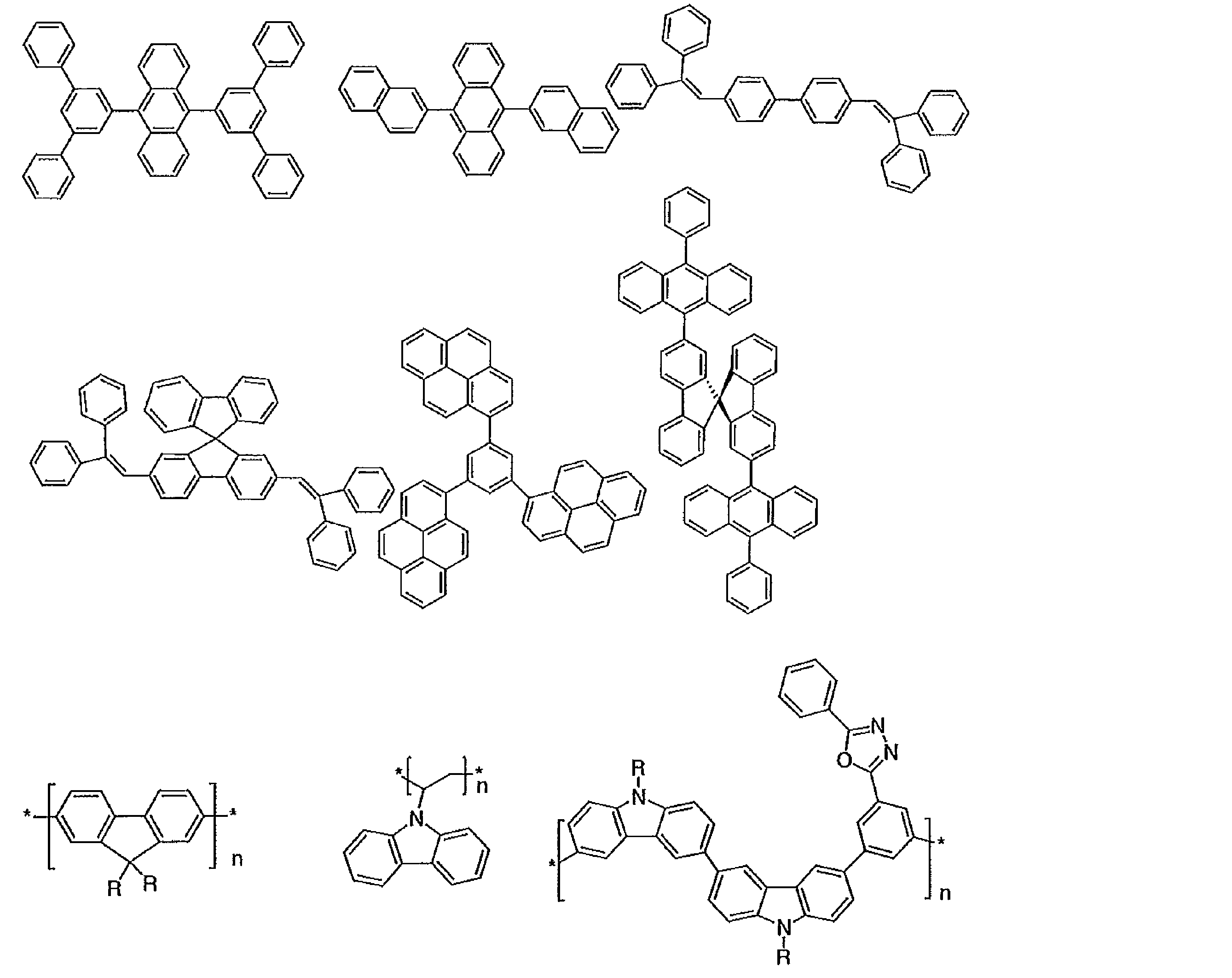

次に、正孔注入材料として用いることができる好ましい化合物例を挙げる。
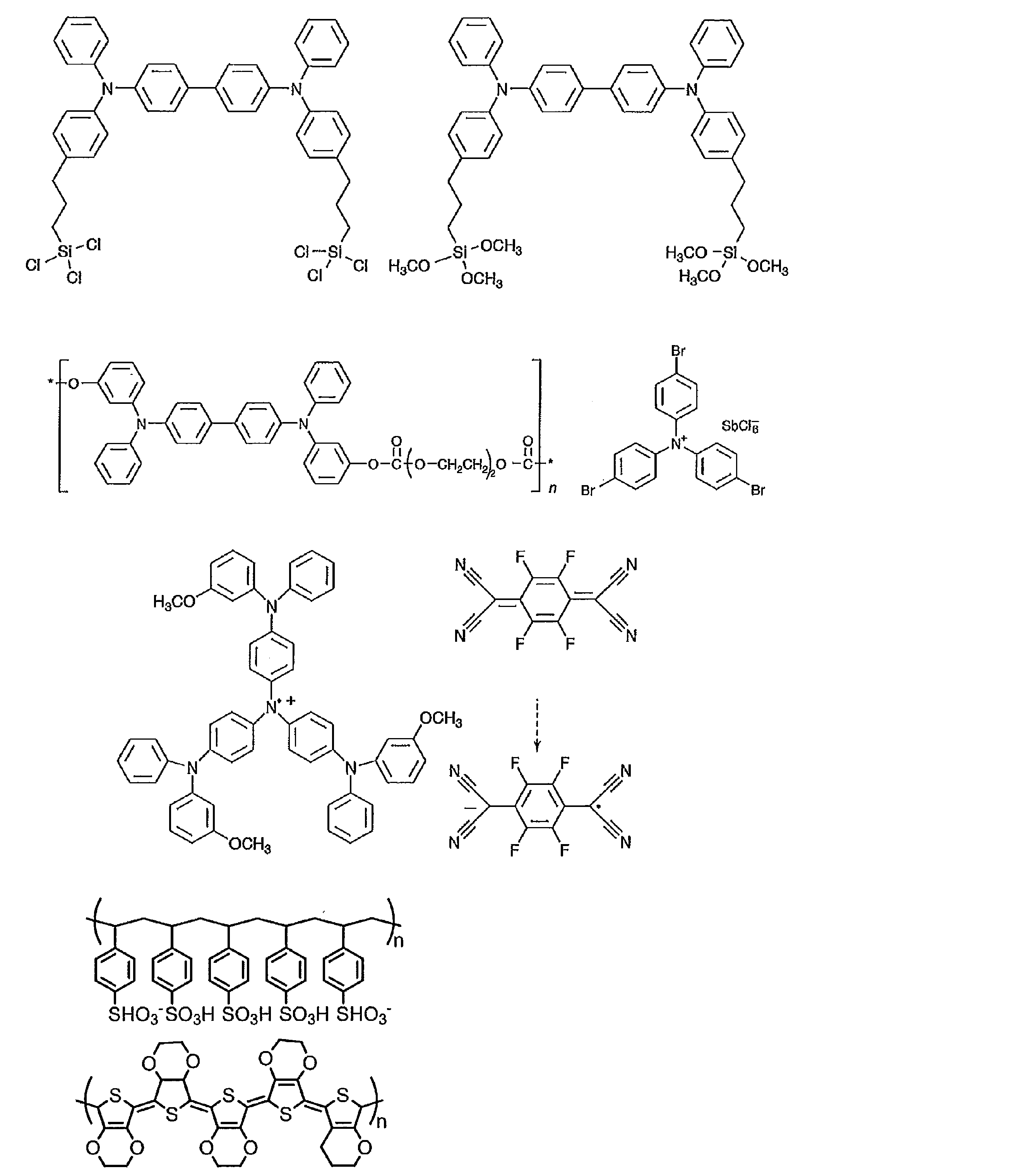
次に、正孔輸送材料として用いることができる好ましい化合物例を挙げる。


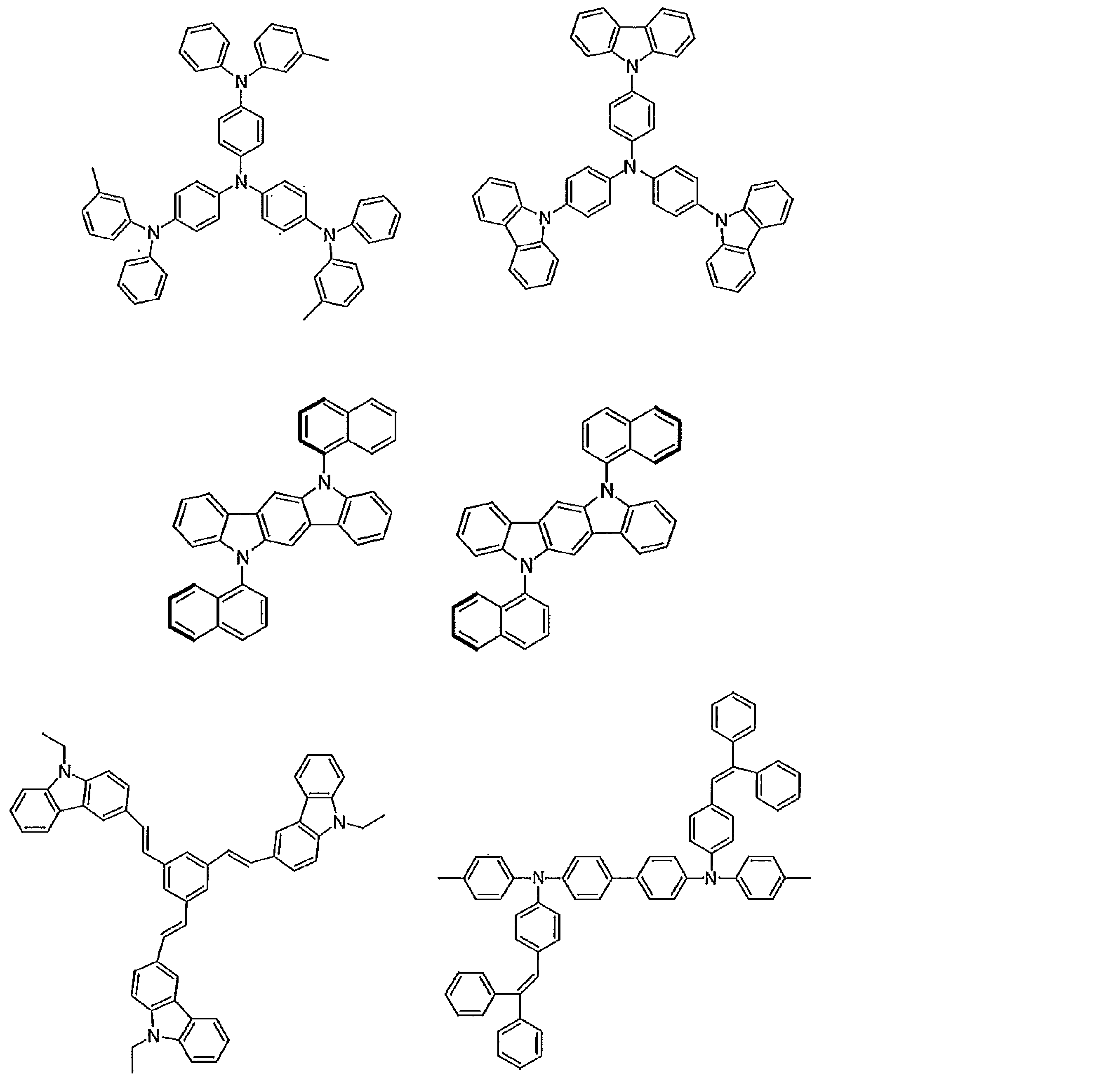


次に、電子阻止材料として用いることができる好ましい化合物例を挙げる。
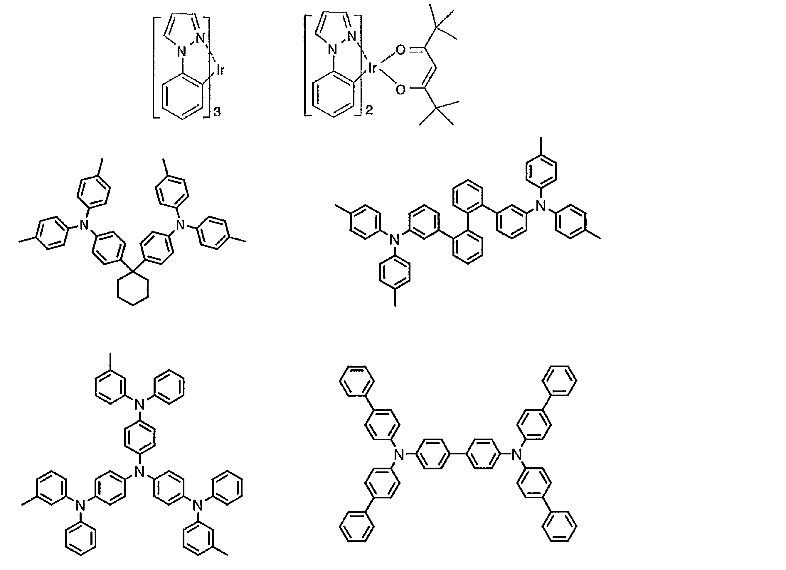
次に、正孔阻止材料として用いることができる好ましい化合物例を挙げる。

次に、電子輸送材料として用いることができる好ましい化合物例を挙げる。
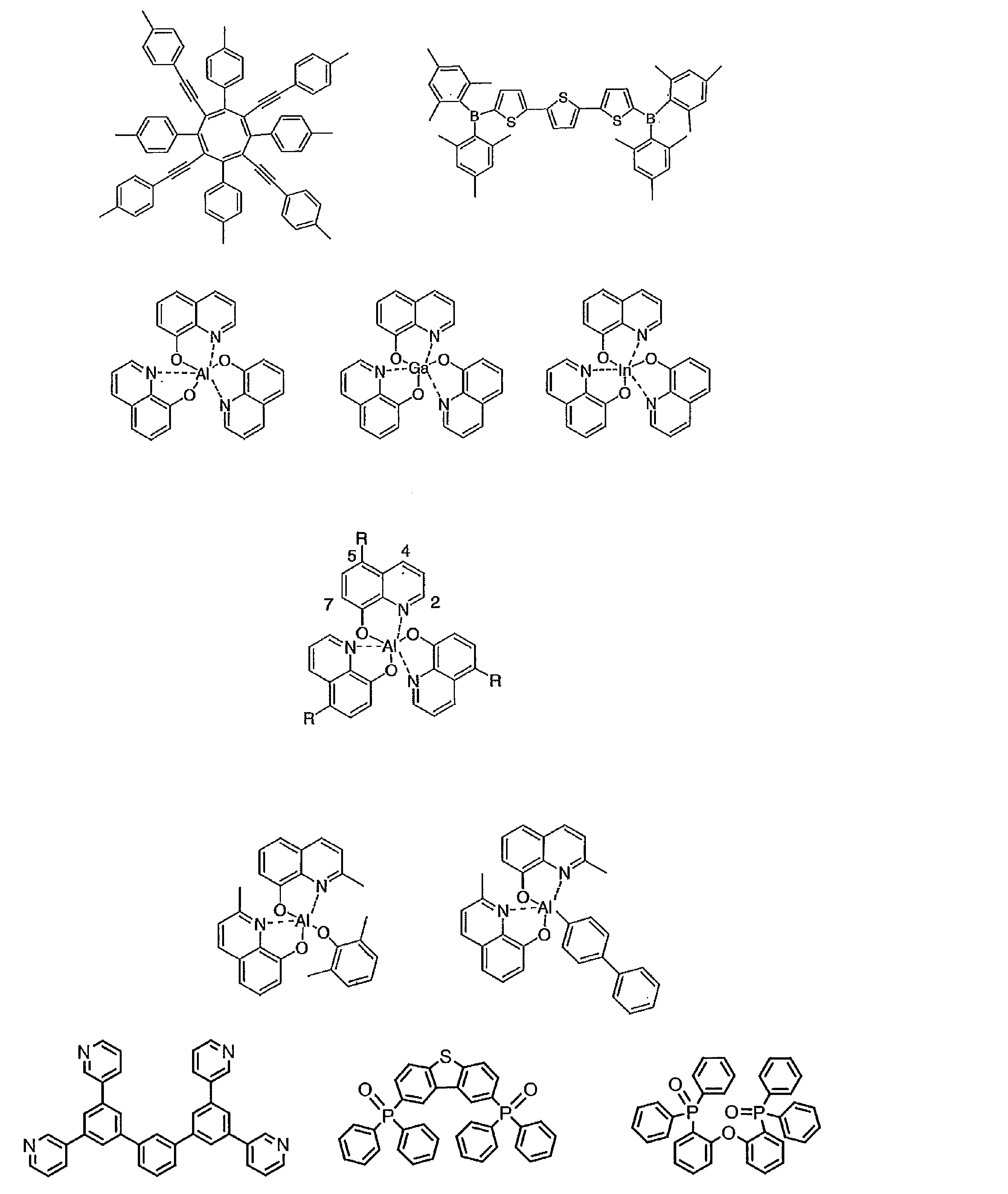


次に、電子注入材料として用いることができる好ましい化合物例を挙げる。

さらに添加可能な材料として好ましい化合物例を挙げる。例えば、安定化材料として添加すること等が考えられる。
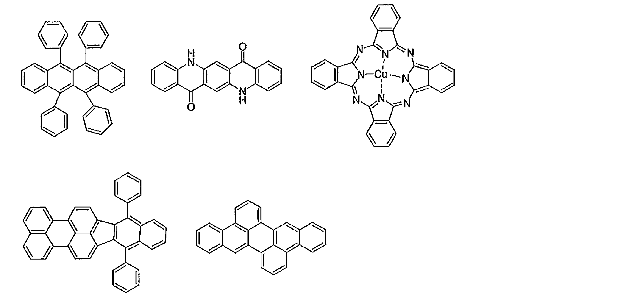
上述の方法により作製された有機エレクトロルミネッセンス素子は、得られた素子の陽極と陰極の間に電界を印加することにより発光する。このとき、励起一重項エネルギーによる発光であれば、そのエネルギーレベルに応じた波長の光が、蛍光発光および遅延蛍光発光として確認される。また、励起三重項エネルギーによる発光であれば、そのエネルギーレベルに応じた波長が、りん光として確認される。通常の蛍光は、遅延蛍光発光よりも蛍光寿命が短いため、発光寿命は蛍光と遅延蛍光で区別できる。
一方、りん光については、本発明の化合物のような通常の有機化合物では、励起三重項エネルギーは不安定で熱等に変換され、寿命が短く直ちに失活するため、室温では殆ど観測できない。通常の有機化合物の励起三重項エネルギーを測定するためには、極低温の条件での発光を観測することにより測定可能である。
一方、りん光については、本発明の化合物のような通常の有機化合物では、励起三重項エネルギーは不安定で熱等に変換され、寿命が短く直ちに失活するため、室温では殆ど観測できない。通常の有機化合物の励起三重項エネルギーを測定するためには、極低温の条件での発光を観測することにより測定可能である。
本発明の有機エレクトロルミネッセンス素子は、単一の素子、アレイ状に配置された構造からなる素子、陽極と陰極がX-Yマトリックス状に配置された構造のいずれにおいても適用することができる。本発明によれば、発光層に一般式(1)で表される化合物を含有させることにより、発光効率が大きく改善された有機発光素子が得られる。本発明の有機エレクトロルミネッセンス素子などの有機発光素子は、さらに様々な用途へ応用することが可能である。例えば、本発明の有機エレクトロルミネッセンス素子を用いて、有機エレクトロルミネッセンス表示装置を製造することが可能であり、詳細については、時任静士、安達千波矢、村田英幸共著「有機ELディスプレイ」(オーム社)を参照することができる。また、特に本発明の有機エレクトロルミネッセンス素子は、需要が大きい有機エレクトロルミネッセンス照明やバックライトに応用することもできる。
以下に合成例および実施例を挙げて本発明の特徴をさらに具体的に説明する。以下に示す材料、処理内容、処理手順等は、本発明の趣旨を逸脱しない限り適宜変更することができる。したがって、本発明の範囲は以下に示す具体例により限定的に解釈されるべきものではない。
なお、各材料の一重項エネルギー(ES1)と三重項エネルギー(ET1)の差(ΔEST)は、一重項エネルギー(ES1)と三重項エネルギーを以下の方法で算出し、ΔEST=ES1-ET1により求めたものである。
(1)一重項エネルギーES1
測定対象化合物とmCBPとを、測定対象化合物が濃度6重量%となるように共蒸着することでSi基板上に厚さ100nmの試料を作製した。常温(300K)でこの試料の蛍光スペクトルを測定した。励起光入射直後から入射後100ナノ秒までの発光を積算することで、縦軸を発光強度、横軸を波長の蛍光スペクトルを得た。蛍光スペクトルは、縦軸を発光、横軸を波長とした。この発光スペクトルの短波側の立ち上がりに対して接線を引き、その接線と横軸との交点の波長値 λedge[nm]を求めた。この波長値を次に示す換算式でエネルギー値に換算した値をES1とした。
換算式:ES1[eV]=1239.85/λedge
発光スペクトルの測定には、励起光源に窒素レーザー(Lasertechnik Berlin社製、MNL200)を検出器には、ストリークカメラ(浜松ホトニクス社製、C4334)を用いた。
(2) 三重項エネルギーET1
一重項エネルギーES1と同じ試料を5[K]に冷却し、励起光(337nm)を燐光測定用試料に照射し、ストリークカメラを用いて、燐光強度を測定した。励起光入射後1ミリ秒から入射後10ミリ秒の発光を積算することで、縦軸を発光強度、横軸を波長の燐光スペクトルを得た。この燐光スペクトルの短波長側の立ち上がりに対して接線を引き、その接線と横軸との交点の波長値λedge[nm]を求めた。この波長値を次に示す換算式でエネルギー値に換算した値をET1とした。
換算式:ET1[eV]=1239.85/λedge
燐光スペクトルの短波長側の立ち上がりに対する接線は以下のように引いた。燐光スペクトルの短波長側から、スペクトルの極大値のうち、最も短波長側の極大値までスペクトル曲線上を移動する際に、長波長側に向けて曲線上の各点における接線を考える。この接線は、曲線が立ち上がるにつれ(つまり縦軸が増加するにつれ)、傾きが増加する。この傾きの値が極大値をとる点において引いた接線を、当該燐光スペクトルの短波長側の立ち上がりに対する接線とした。
なお、スペクトルの最大ピーク強度の10%以下のピーク強度をもつ極大点は、上述の最も短波長側の極大値には含めず、最も短波長側の極大値に最も近い、傾きの値が極大値をとる点において引いた接線を当該燐光スペクトルの短波長側の立ち上がりに対する接線とした。
(合成例1) 化合物1の合成

窒素置換した二つ口フラスコに、5,10-ジヒドロフェナジン(364mg,2.00mmol)、2-(4-ブロモフェニル)-4,6-ジフェニル-1,3,5-トリアジン(1.71g,4.40mmol)、炭酸カリウム(1.66g,12.0mmol)、トルエン20mlを加え、室温下10分間攪拌した.そこに酢酸パラジウム(II)(26.9mg,0.12mmol)、トリーtertーブチルホスフィン(89.0mg,0.44mmol)、トルエン20mlの混合溶液を加え、24時間加熱・還流した.室温まで放冷した後、クロロホルムと食塩水を加え、有機層を分液・抽出した.無水硫酸マグネシウムを加え脱水し、溶媒を減圧下留去すると赤色固体が得られた.ヘキサンで固体を洗い、減圧下乾燥することにより目的物である5,10-ビス{4-(2,4-ジフェニル-1,3,5-トリアジル)-フェニル}-フェナジンを得た(収量:1.52g,収率:95.5%)。
MALDI-MS m/z 計算値(C54H36N8): 797; 実測値: 797
元素分析:計算値(C54H36N8): C, 81.39; H, 4.55; N, 14.06; 実測値: C, 81.53; H, 4.49; N, 14.05.
MALDI-MS m/z 計算値(C54H36N8): 797; 実測値: 797
元素分析:計算値(C54H36N8): C, 81.39; H, 4.55; N, 14.06; 実測値: C, 81.53; H, 4.49; N, 14.05.
(合成例2) 化合物2の合成
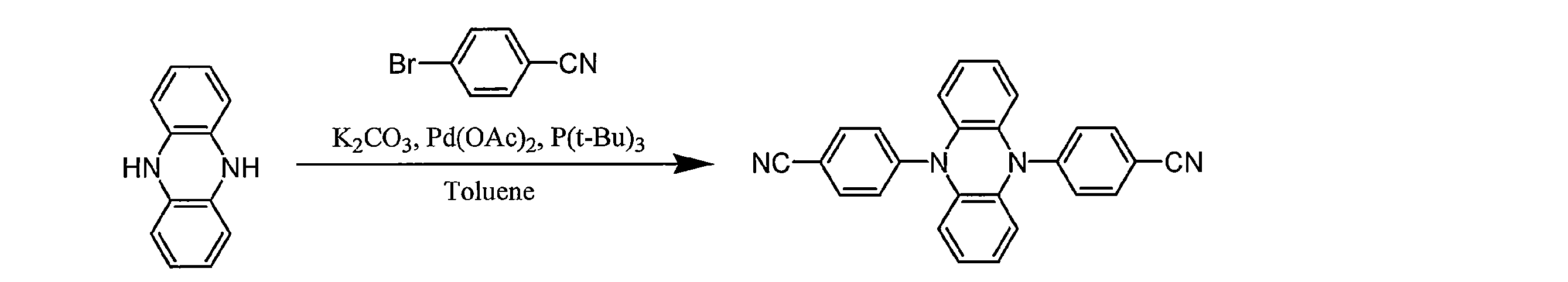
窒素置換した二つ口フラスコに、5,10-ジヒドロフェナジン(364mg,2.00mmol)、4-ブロモベンゾニトリル(801mg,4.40mmol)、炭酸カリウム(1.66g,12.0mmol)、トルエン20mlを加え、室温下10分間攪拌した.そこに酢酸パラジウム(II)(26.9mg,0.12mmol)、トリーtertーブチルホスフィン(89.0mg,0.44mmol)、トルエン20mlの混合溶液を加え、24時間加熱・還流した.室温まで放冷した後、クロロホルムと食塩水を加え、有機層を分液・抽出した.無水硫酸マグネシウムを加え脱水し、溶媒を減圧下留去すると橙色固体が得られた.ヘキサンで固体を洗い、減圧下乾燥することにより目的物である5,10-ビス(4-シアノフェニル)-フェナジンを得た(収量:720mg,収率:93.6%)。
MALDI-MS m/z計算値 (C26H16N4): 384; 実測値: 384.
元素分析:計算値 (C26H16N4): C, 81.23; H, 4.20; N, 14.57; 実測値: C, 81.27; H, 4.11; N, 14.49.
MALDI-MS m/z計算値 (C26H16N4): 384; 実測値: 384.
元素分析:計算値 (C26H16N4): C, 81.23; H, 4.20; N, 14.57; 実測値: C, 81.27; H, 4.11; N, 14.49.
(合成例3) 化合物3の合成

窒素置換した二つ口フラスコに、5,10-ジヒドロフェナジン(364mg,2.00mmol)、3-ブロモベンゾニトリル(801mg,4.40mmol)、炭酸カリウム(1.66g,12.0mmol)、トルエン20mlを加え、室温下10分間攪拌した.そこに酢酸パラジウム(II)(26.9mg,0.12mmol)、トリーtertーブチルホスフィン(89.0mg,0.44mmol)、トルエン20mlの混合溶液を加え、24時間加熱・還流した.室温まで放冷した後、クロロホルムと食塩水を加え、有機層を分液・抽出した.無水硫酸マグネシウムを加え脱水し、溶媒を減圧下留去した.クロロホルムを用いたシリカゲルカラムクロマトグラフィーにより目的物である5,10-ビス(3-シアノフェニル)-フェナジンを単離・精製した(収量:704mg,収率:91.5%).
(合成例4) 化合物5の合成

窒素置換した二つ口フラスコに、5,10-ジヒドロフェナジン(364mg,2.00mmol)、2-(4-ブロモフェニル)-ベンゾチアゾール(1.28g,4.40mmol)、炭酸カリウム(1.66g,12.0mmol)、トルエン20mlを加え、室温下10分間攪拌した.そこに酢酸パラジウム(II)(26.9mg,0.12mmol)、トリーtertーブチルホスフィン(89.0mg,0.44mmol)、トルエン20mlの混合溶液を加え、24時間加熱・還流した.室温まで放冷した後、クロロホルムと食塩水を加え、有機層を分液・抽出した.無水硫酸マグネシウムを加え脱水し、溶媒を減圧下留去すると赤色固体が得られた.ヘキサンで固体を洗い、減圧下乾燥することにより目的物である5,10-bis{4-(2-ベンゾチアゾリル)-フェニル}-フェナジンを得た(収量:1.01g,収率:84.0%)。
1H NMR (CDCl3, 400 MHz) δ: 5.78(m, 4H), 6.34(m, 4H), 7.44(t, 2H), 7.54(t, 2H), 7.55(d, 4H) 7.95(d, 2H), 8.11(d, 2H), 8.35(d, 4H)
MALDI-MS m/z計算値(C38H24N4S2): 601; 実測値: 600.
元素分析:計算値(C38H24N4S2): C, 75.97; H, 4.03; N, 9.33; 実測値: C, 75.91; H, 4.10; N, 9.28.
1H NMR (CDCl3, 400 MHz) δ: 5.78(m, 4H), 6.34(m, 4H), 7.44(t, 2H), 7.54(t, 2H), 7.55(d, 4H) 7.95(d, 2H), 8.11(d, 2H), 8.35(d, 4H)
MALDI-MS m/z計算値(C38H24N4S2): 601; 実測値: 600.
元素分析:計算値(C38H24N4S2): C, 75.97; H, 4.03; N, 9.33; 実測値: C, 75.91; H, 4.10; N, 9.28.
(合成例5) 化合物6の合成

窒素置換した二つ口フラスコに、5,10-ジヒドロフェナジン(364mg,2.00mmol)、2-(4-ブロモフェニル)-1-フェニル-ベンズイミダゾール(1.54g,4.40mmol)、炭酸カリウム(1.66g,12.0mmol)、トルエン20mlを加え、室温下10分間攪拌した.そこに酢酸パラジウム(II)(26.9mg,0.12mmol)、トリーtertーブチルホスフィン(89.0mg,0.44mmol)、トルエン20mlの混合溶液を加え、24時間加熱・還流した.室温まで放冷した後、クロロホルムと食塩水を加え、有機層を分液・抽出した.無水硫酸マグネシウムを加え脱水し、溶媒を減圧下留去すると赤色固体が得られた.ヘキサンで固体を洗い、減圧下乾燥することにより目的物である5,10-ビス[4-{2-(1-フェニル)-ベンズイミダゾリル}-フェニル]-フェナジンを得た(収量:1.40g,収率:97.3%)。
1H NMR (CDCl3, 400 MHz)δ:7.28(d, 8H), 7.36(m, 10H) 7.39(d, 4H), 7.52(m, 8H), 7.89(d, 4H)
MALDI-MS m/z計算値(C50H34N6): 719; 実測値: 719.
元素分析:計算値(C50H34N6): C, 83.54; H, 4.77; N, 11.69; 実測値: C, 83.62; H, 4.72; N, 11.68.
1H NMR (CDCl3, 400 MHz)δ:7.28(d, 8H), 7.36(m, 10H) 7.39(d, 4H), 7.52(m, 8H), 7.89(d, 4H)
MALDI-MS m/z計算値(C50H34N6): 719; 実測値: 719.
元素分析:計算値(C50H34N6): C, 83.54; H, 4.77; N, 11.69; 実測値: C, 83.62; H, 4.72; N, 11.68.
(実施例1) 有機フォトルミネッセンス素子の作製と評価(溶液)
合成例1で合成した化合物1のトルエン溶液(濃度10-5mol/L)を調製して、窒素をバブリングしながら300Kで紫外光を照射したところ、586nmの蛍光が観測された。また、窒素バブル前後にトルエン溶液中でのフォトルミネッセンス量子効率を絶対PL量子収率測定装置(浜松ホトニクス(株)製Quantaurus-QY)により300Kで測定したところ、窒素バブル前が3.4%であり、窒素バブル後が5.5%であった。
化合物1のかわりに合成例2で合成した化合物2のトルエン溶液(濃度10-5mol/L)を調製して、窒素をバブリングしながら300Kで紫外光を照射したところ、545nmの蛍光が観測された(通常蛍光τp=6.28ns、遅延蛍光τd=1.88μs)。また、フォトルミネッセンス量子効率は、窒素バブル前が3.3%であり、窒素バブル後が8.4%であった。
合成例3で合成した化合物3のトルエン溶液(濃度10-5mol/L)を調製して、窒素をバブリングしながら300Kで紫外光を照射したところ、555nmの蛍光が観測された。また、フォトルミネッセンス量子効率は、窒素バブル前が1.9%であり、窒素バブル後が2.3%であった。
合成例5で合成した化合物5のトルエン溶液(濃度10-5mol/L)を調製して、窒素をバブリングしながら300Kで紫外光を照射したところ、605nmの蛍光が観測された(τp=6.85ns、τd=0.24μs)。また、フォトルミネッセンス量子効率は、窒素バブル前が4.7%であり、窒素バブル後が9.7%であった。
合成例6で合成した化合物6のトルエン溶液(濃度10-5mol/L)を調製して、窒素をバブリングしながら300Kで紫外光を照射したところ、554nmの蛍光が観測された(τp=6.75ns、τd=5.71μs)。また、フォトルミネッセンス量子効率は、窒素バブル前が7.3%であり、窒素バブル後が31.4%であった。
(実施例2) 有機フォトルミネッセンス素子の作製と評価(薄膜)
シリコン基板上に真空蒸着法にて、真空度5.0×10⁻⁴Paの条件にて化合物1とmCBPとを異なる蒸着源から蒸着し、化合物1の濃度が6.0重量%である薄膜を0.3nm/秒にて100nmの厚さで形成して有機フォトルミネッセンス素子とした。50K、100K、150K、200K、250K、300Kの各温度における過渡減衰曲線を図2に示す。化合物1が熱活性型遅延蛍光材料であることが確認された。300Kにおけるτpは6.24nsであり、τdは0.14μsであった。
化合物1のかわりに化合物2を用いて有機フォトルミネッセンス素子を作製して、同様に測定を行った。50K、100K、150K、200K、250K、300Kの各温度における過渡減衰曲線を図3に示す。化合物2が熱活性型遅延蛍光材料であることが確認された。300Kにおけるτpは6.83nsであり、τdは6.69μsであった。また、実施例1と同じ測定装置を用いて得たフォトルミネッセンス量子効率は300Kで35.2%であった(通常蛍光16.8%、遅延蛍光18.4%)。ΔESTは0.10eVであった。
化合物1のかわりに化合物5を用いて有機フォトルミネッセンス素子を作製して、同様に測定を行った。50K、100K、150K、200K、250K、300Kの各温度における過渡減衰曲線を図4に示す。化合物5が熱活性型遅延蛍光材料であることが確認された。300Kにおけるτpは12.18nsであり、τdは1.10μsであった。また、実施例1と同じ測定装置を用いて得たフォトルミネッセンス量子効率は300Kで33.0%であった(通常蛍光20.6%、遅延蛍光12.4%)。ΔESTは0.03eVであった。
化合物1のかわりに化合物6を用いて有機フォトルミネッセンス素子を作製して、同様に測定を行った。50K、100K、150K、200K、250K、300Kの各温度における過渡減衰曲線を図5に示す。化合物6が熱活性型遅延蛍光材料であることが確認された。300Kにおけるτpは4.12nsであり、τdは53.00μsであった。また、実施例1と同じ測定装置を用いて得たフォトルミネッセンス量子効率は300Kで67.6%であった(通常蛍光34.0%、遅延蛍光33.6%)。ΔESTは0.19eVであった。
(実施例3) 有機エレクトロルミネッセンス素子の作製と評価
膜厚100nmのインジウム・スズ酸化物(ITO)からなる陽極が形成されたガラス基板上に、各薄膜を真空蒸着法にて、真空度5.0×10⁻⁴Paで積層した。まず、ITO上にα-NPDを35nmの厚さに形成した。次に、化合物1とCBPを異なる蒸着源から共蒸着し、15nmの厚さの層を形成して発光層とした。この時、化合物1の濃度は2.0重量%とした。次に、TPBiを65nmの厚さに形成し、さらにフッ化リチウム(LiF)を0.5nm真空蒸着し、次いでアルミニウム(Al)を100nmの厚さに蒸着することにより陰極を形成し、有機エレクトロルミネッセンス素子とした。
製造した有機エレクトロルミネッセンス素子を、半導体パラメータ・アナライザ(アジレント・テクノロジー社製:E5273A)、光パワーメータ測定装置(ニューポート社製:1930C)、および光学分光器(オーシャンオプティクス社製:USB2000)を用いて測定したところ、図6に示すように600nmの発光が認められた。電流密度-電圧特性を図7に示す。
化合物1のかわりに化合物2を用いて、発光層の化合物2の濃度が2.0重量%の有機エレクトロミネッセンス素子と、発光層の化合物2の濃度が6.0重量%の有機エレクトロミネッセンス素子を作製した。発光スペクトルを図8に示し、電流密度-電圧特性を図9に示し、輝度-外部量子効率特性を図10に示し、電流密度-外部量子効率特性を図11に示す。化合物2を発光材料として用いた有機エレクトロルミネッセンス素子は8.8%の高い外部量子効率を達成した。
化合物1のかわりに化合物6を用いて、発光層の化合物6の濃度が2.0重量%の有機エレクトロミネッセンス素子を作製した。発光スペクトルを図13に示し、電流密度-電圧特性を図14に示し、電流密度-外部量子効率特性を図15に示す。化合物6を発光材料として用いた有機エレクトロルミネッセンス素子は11.3%の高い外部量子効率を達成した。また、発光層の化合物6の濃度が6.0重量%の有機エレクトロミネッセンス素子を作製したときの電流密度-外部量子効率特性を図12に示す。この有機エレクトロルミネッセンス素子は12.1%の高い外部量子効率を達成した。
(比較例1) 有機エレクトロルミネッセンス素子の作製と評価
実施例3における化合物1のかわりに、下記の構造を有する比較化合物を用いて有機エレクトロミネッセンス素子を作製した。この有機エレクトロミネッセンス素子はまったく発光しなかった。
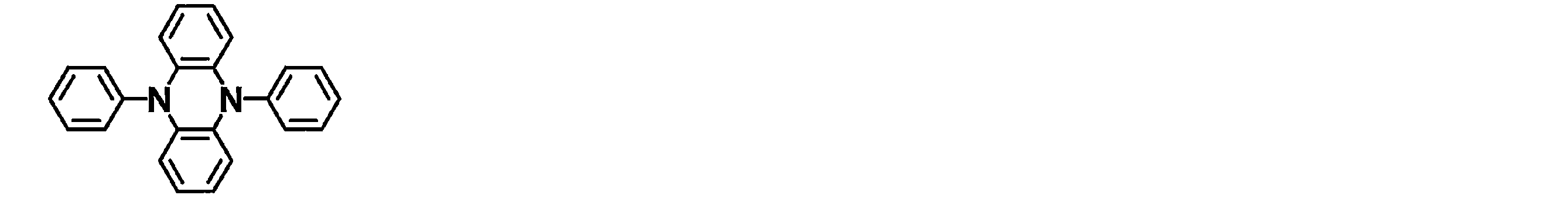
実施例3における化合物1のかわりに、下記の構造を有する比較化合物を用いて有機エレクトロミネッセンス素子を作製した。この有機エレクトロミネッセンス素子はまったく発光しなかった。

本発明の化合物は発光材料として有用である。このため本発明の化合物は、有機エレクトロルミネッセンス素子などの有機発光素子用の発光材料として効果的に用いられる。本発明の化合物の中には、遅延蛍光を放射するものも含まれているため、発光効率が高い有機発光素子を提供することも可能である。このため、本発明は産業上の利用可能性が高い。
1 基板
2 陽極
3 正孔注入層
4 正孔輸送層
5 発光層
6 電子輸送層
7 陰極
2 陽極
3 正孔注入層
4 正孔輸送層
5 発光層
6 電子輸送層
7 陰極
Claims (12)
- 下記一般式(1)で表される化合物。
一般式(1)
A-D-A
[一般式(1)において、Dは下記式:

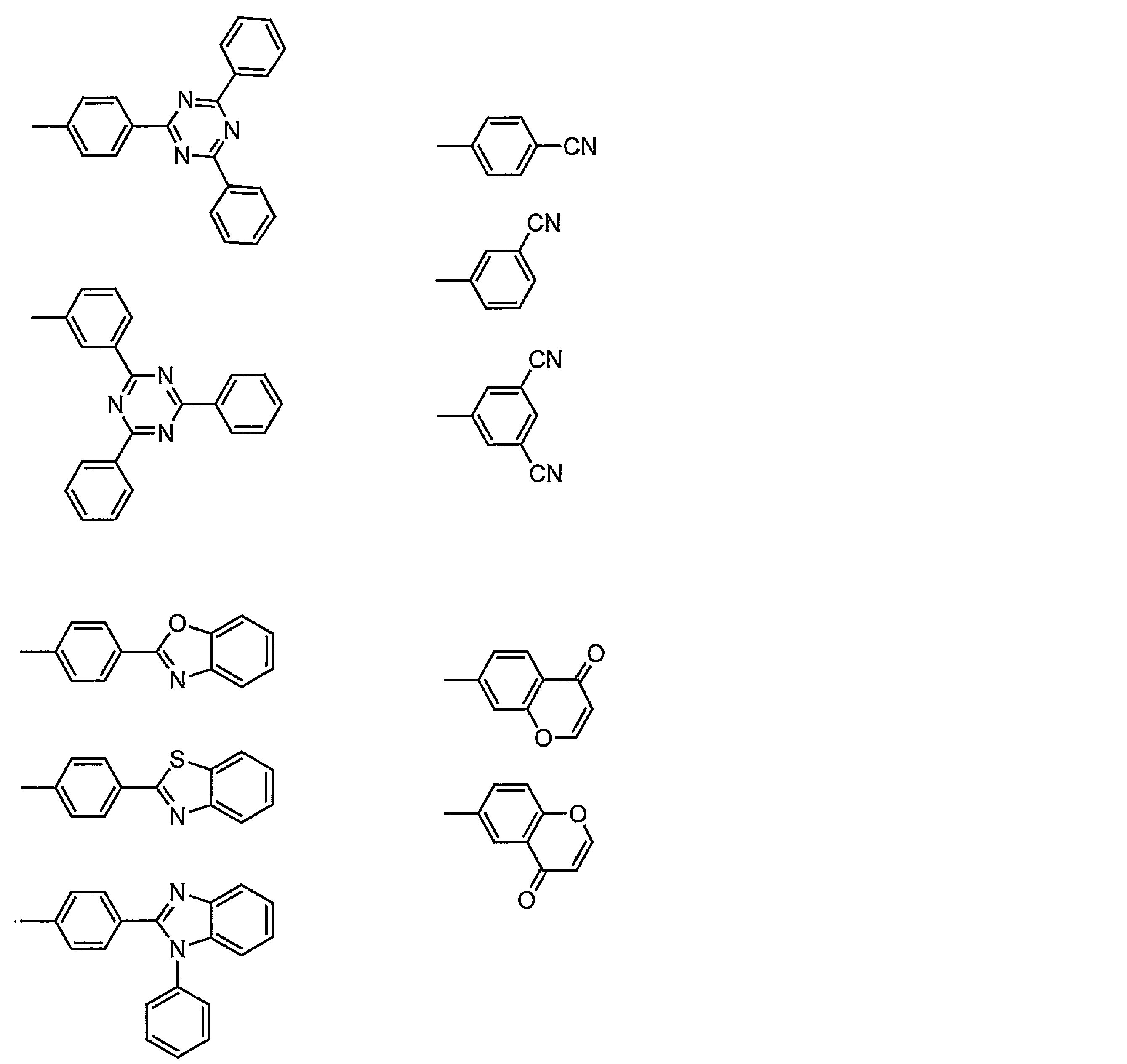
- 一般式(1)のDが下記一般式(2)で表される構造を有することを特徴とする請求項1に記載の化合物。
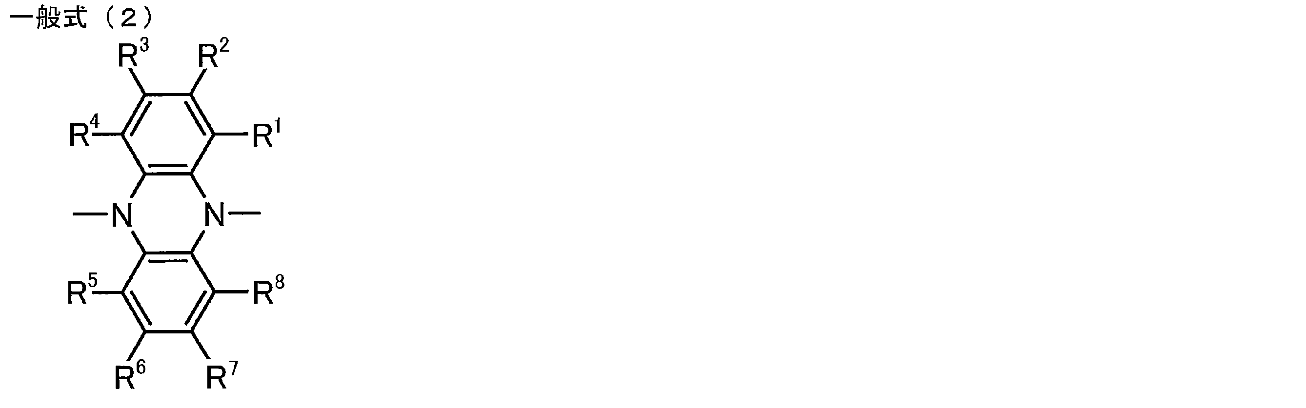
- 一般式(1)の2つのAが同一の構造を有することを特徴とする請求項1または2に記載の化合物。
- 下記一般式(3)で表されることを特徴とする請求項1~3のいずれか1項に記載の化合物。

<1> R12がシアノ基または下記構造の基(ただし水素原子は置換基で置換されていてもよい)であるか、


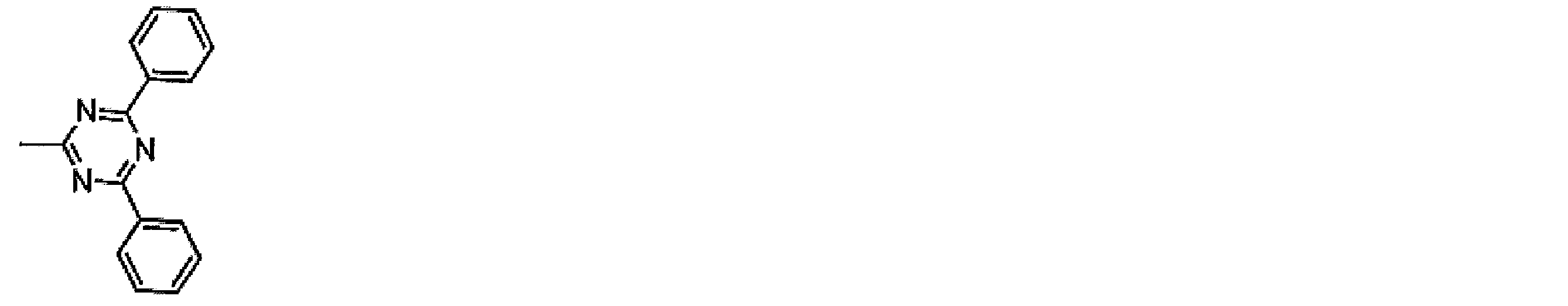

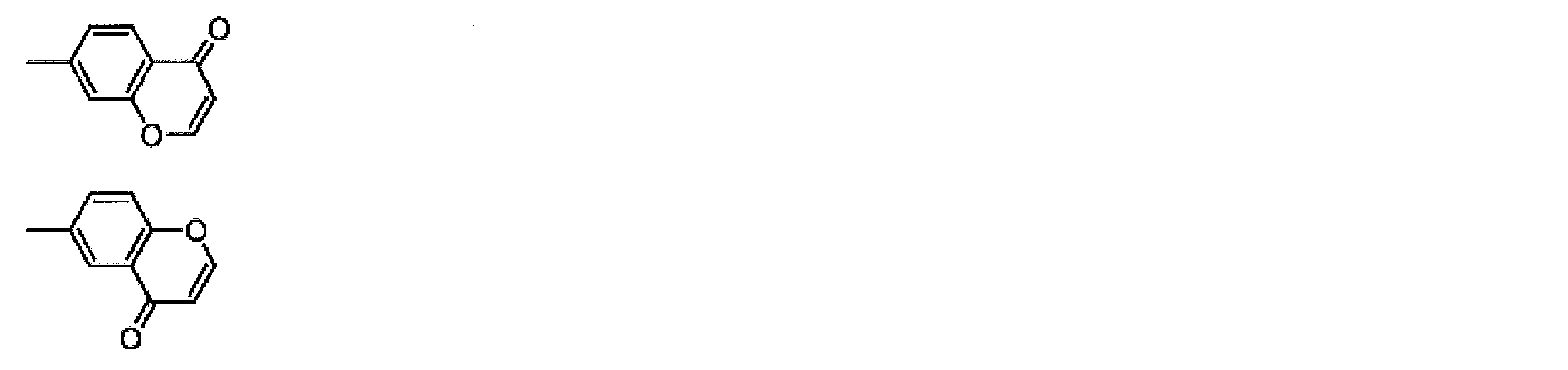
- 一般式(3)のR1~R8が、各々独立に水素原子、炭素数1~10の置換もしくは無置換のアルキル基、炭素数1~10の置換もしくは無置換のアルコキシ基、炭素数6~15の置換もしくは無置換のアリール基、または炭素数3~12の置換もしくは無置換のヘテロアリール基であることを特徴とする請求項4に記載の化合物。
- 一般式(3)のR12、R13、R17、R18のうちの少なくとも2つが上記<1>および<2>の条件を満たすように置換基を有しており、それ以外のR11~R18が各々独立に水素原子、フッ素原子、塩素原子、シアノ基、炭素数1~10の置換もしくは無置換のアルキル基、炭素数1~10の置換もしくは無置換のアルコキシ基、炭素数1~10の置換もしくは無置換のジアルキルアミノ基、炭素数12~40の置換もしくは無置換のジアリールアミノ基、炭素数6~15の置換もしくは無置換のアリール基、または炭素数3~12の置換もしくは無置換のヘテロアリール基であることを特徴とする請求項4または5に記載の化合物。
- 一般式(3)の上記<1>および<2>中に記載される構造の水素原子が置換されていてもよい置換基が、フッ素原子、塩素原子、シアノ基、炭素数1~10の置換もしくは無置換のアルキル基、炭素数1~10の置換もしくは無置換のアルコキシ基、炭素数1~10の置換もしくは無置換のジアルキルアミノ基、炭素数12~40の置換もしくは無置換のジアリールアミノ基、炭素数6~15の置換もしくは無置換のアリール基、および炭素数3~12の置換もしくは無置換のヘテロアリール基からなる群より選択されることを特徴とする請求項4~6のいずれか1項に記載の化合物。
- 請求項1~7のいずれか1項に記載の化合物からなる発光材料。
- 下記一般式(1)で表される構造を有する遅延蛍光体。
一般式(1)
A-D-A
[一般式(1)において、Dは下記式:

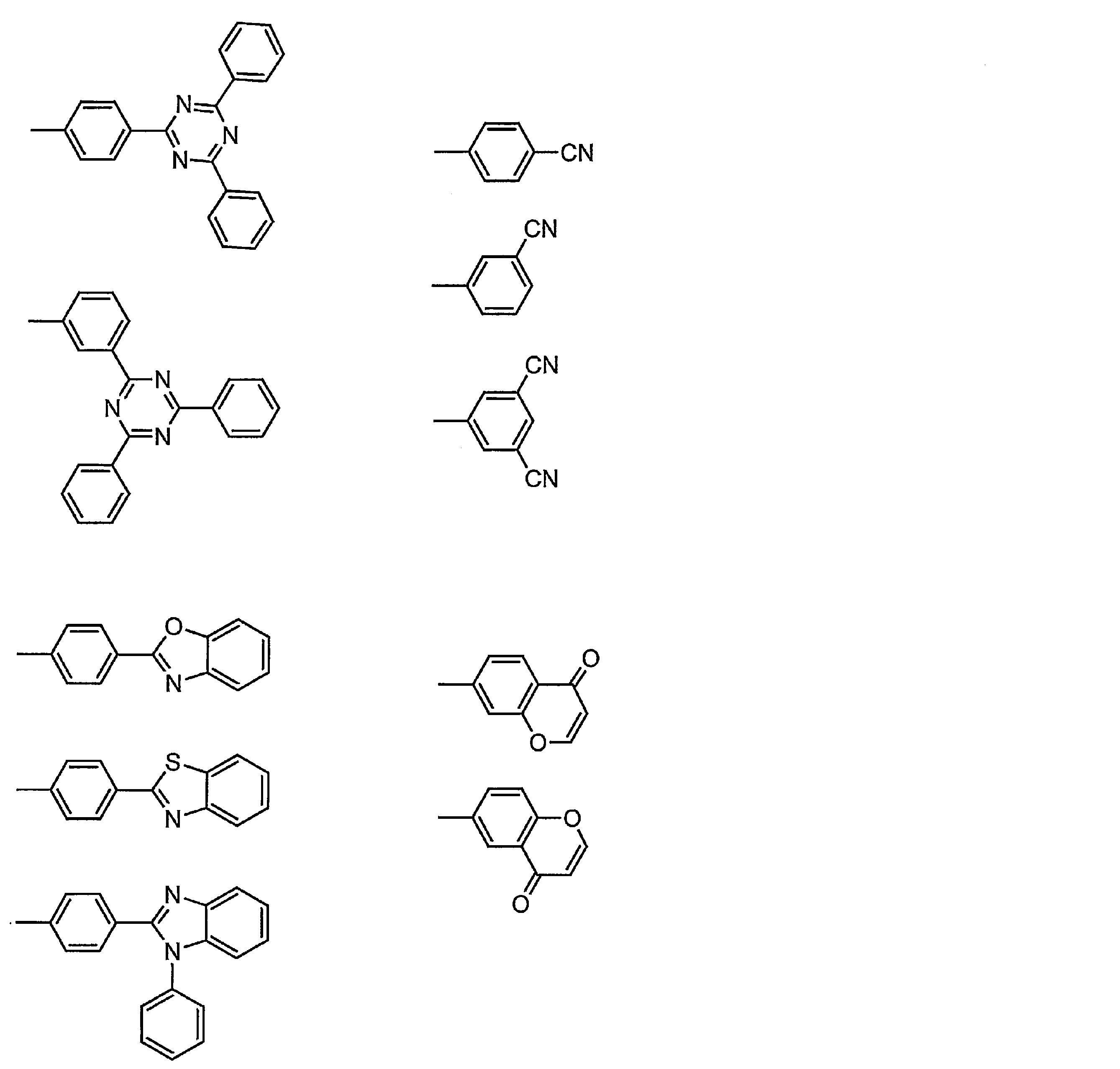
- 請求項8に記載の発光材料を含む発光層を基板上に有することを特徴とする有機発光素子。
- 遅延蛍光を放射することを特徴とする請求項10に記載の有機発光素子。
- 有機エレクトロルミネッセンス素子であることを特徴とする請求項10または11に記載の有機発光素子。
Priority Applications (1)
| Application Number | Priority Date | Filing Date | Title |
|---|---|---|---|
| JP2015518295A JP6277182B2 (ja) | 2013-05-24 | 2014-05-23 | 化合物、発光材料および有機発光素子 |
Applications Claiming Priority (2)
| Application Number | Priority Date | Filing Date | Title |
|---|---|---|---|
| JP2013110382 | 2013-05-24 | ||
| JP2013-110382 | 2013-05-24 |
Publications (1)
| Publication Number | Publication Date |
|---|---|
| WO2014189122A1 true WO2014189122A1 (ja) | 2014-11-27 |
Family
ID=51933673
Family Applications (1)
| Application Number | Title | Priority Date | Filing Date |
|---|---|---|---|
| PCT/JP2014/063638 WO2014189122A1 (ja) | 2013-05-24 | 2014-05-23 | 化合物、発光材料および有機発光素子 |
Country Status (3)
| Country | Link |
|---|---|
| JP (1) | JP6277182B2 (ja) |
| TW (1) | TW201509920A (ja) |
| WO (1) | WO2014189122A1 (ja) |
Cited By (20)
| Publication number | Priority date | Publication date | Assignee | Title |
|---|---|---|---|---|
| WO2016111196A1 (ja) * | 2015-01-08 | 2016-07-14 | 国立大学法人九州大学 | 化合物、混合物、発光層、有機発光素子およびアシストドーパント |
| JP2016130231A (ja) * | 2015-01-08 | 2016-07-21 | 国立大学法人九州大学 | 化合物、混合物、発光層、有機発光素子およびアシストドーパント |
| WO2019218347A1 (en) * | 2018-05-18 | 2019-11-21 | Soochow University | Oligomer of n,n'-di(hetero)aryl-5,10-dihydrophenazine, cathode active material, cathode, battery thereof, and process for preparing same |
| WO2020076796A1 (en) | 2018-10-09 | 2020-04-16 | Kyulux, Inc. | Novel composition of matter for use in organic light-emitting diodes |
| WO2021157642A1 (ja) | 2020-02-04 | 2021-08-12 | 株式会社Kyulux | ホスト材料、組成物および有機発光素子 |
| US11101440B2 (en) | 2015-07-01 | 2021-08-24 | Kyushu University, National University Corporation | Organic electroluminescent device |
| WO2021235549A1 (ja) | 2020-05-22 | 2021-11-25 | 株式会社Kyulux | 化合物、発光材料および発光素子 |
| WO2022025248A1 (ja) | 2020-07-31 | 2022-02-03 | 株式会社Kyulux | 化合物、発光材料および発光素子 |
| US11335872B2 (en) | 2016-09-06 | 2022-05-17 | Kyulux, Inc. | Organic light-emitting device |
| WO2022168956A1 (ja) | 2021-02-04 | 2022-08-11 | 株式会社Kyulux | 化合物、発光材料および有機発光素子 |
| US11476435B2 (en) | 2017-08-24 | 2022-10-18 | Kyushu University, National University Corporation | Film and organic light-emitting device containing perovskite-type compound and organic light-emitting material |
| US11482679B2 (en) | 2017-05-23 | 2022-10-25 | Kyushu University, National University Corporation | Compound, light-emitting lifetime lengthening agent, use of n-type compound, film and light-emitting device |
| WO2022244503A1 (ja) | 2021-05-20 | 2022-11-24 | 株式会社Kyulux | 有機発光素子 |
| WO2022270602A1 (ja) | 2021-06-23 | 2022-12-29 | 株式会社Kyulux | 有機発光素子および膜 |
| WO2022270354A1 (ja) | 2021-06-23 | 2022-12-29 | 株式会社Kyulux | 化合物、発光材料および有機発光素子 |
| WO2023282224A1 (ja) | 2021-07-06 | 2023-01-12 | 株式会社Kyulux | 有機発光素子およびその設計方法 |
| WO2023053835A1 (ja) | 2021-09-28 | 2023-04-06 | 株式会社Kyulux | 化合物、組成物、ホスト材料、電子障壁材料および有機発光素子 |
| US11692065B2 (en) | 2019-03-29 | 2023-07-04 | Cornell University | Phenazine copolymers and uses thereof |
| US11795185B2 (en) | 2017-12-13 | 2023-10-24 | Lg Display Co., Ltd. | Compound for electron-transport material and organic light emitting diode including the same |
| US11930654B2 (en) | 2017-07-06 | 2024-03-12 | Kyulux, Inc. | Organic light-emitting element |
Families Citing this family (2)
| Publication number | Priority date | Publication date | Assignee | Title |
|---|---|---|---|---|
| CN110299460B (zh) * | 2019-06-24 | 2020-11-24 | 武汉华星光电半导体显示技术有限公司 | 一种空穴传输材料、制备方法及电致发光器件 |
| US11355713B2 (en) | 2019-06-24 | 2022-06-07 | Wuhan China Star Optoelectronics Semiconductor Display Technology Co., Ltd. | Hole transport material, manufacturing method thereof, and electroluminescent device thereof |
Citations (3)
| Publication number | Priority date | Publication date | Assignee | Title |
|---|---|---|---|---|
| WO2012067415A2 (ko) * | 2010-11-19 | 2012-05-24 | 덕산하이메탈(주) | 화합물 및 이를 이용한 유기전기소자, 그 단말 |
| WO2013172255A1 (ja) * | 2012-05-17 | 2013-11-21 | 国立大学法人九州大学 | 化合物、発光材料および有機発光素子 |
| WO2014034535A1 (ja) * | 2012-08-30 | 2014-03-06 | 国立大学法人九州大学 | 発光材料、化合物、およびそれらを用いた有機発光素子 |
-
2014
- 2014-05-23 JP JP2015518295A patent/JP6277182B2/ja active Active
- 2014-05-23 WO PCT/JP2014/063638 patent/WO2014189122A1/ja active Application Filing
- 2014-05-23 TW TW103118144A patent/TW201509920A/zh unknown
Patent Citations (3)
| Publication number | Priority date | Publication date | Assignee | Title |
|---|---|---|---|---|
| WO2012067415A2 (ko) * | 2010-11-19 | 2012-05-24 | 덕산하이메탈(주) | 화합물 및 이를 이용한 유기전기소자, 그 단말 |
| WO2013172255A1 (ja) * | 2012-05-17 | 2013-11-21 | 国立大学法人九州大学 | 化合物、発光材料および有機発光素子 |
| WO2014034535A1 (ja) * | 2012-08-30 | 2014-03-06 | 国立大学法人九州大学 | 発光材料、化合物、およびそれらを用いた有機発光素子 |
Cited By (22)
| Publication number | Priority date | Publication date | Assignee | Title |
|---|---|---|---|---|
| JP2016130231A (ja) * | 2015-01-08 | 2016-07-21 | 国立大学法人九州大学 | 化合物、混合物、発光層、有機発光素子およびアシストドーパント |
| WO2016111196A1 (ja) * | 2015-01-08 | 2016-07-14 | 国立大学法人九州大学 | 化合物、混合物、発光層、有機発光素子およびアシストドーパント |
| US11101440B2 (en) | 2015-07-01 | 2021-08-24 | Kyushu University, National University Corporation | Organic electroluminescent device |
| US11335872B2 (en) | 2016-09-06 | 2022-05-17 | Kyulux, Inc. | Organic light-emitting device |
| US11482679B2 (en) | 2017-05-23 | 2022-10-25 | Kyushu University, National University Corporation | Compound, light-emitting lifetime lengthening agent, use of n-type compound, film and light-emitting device |
| US11930654B2 (en) | 2017-07-06 | 2024-03-12 | Kyulux, Inc. | Organic light-emitting element |
| US11476435B2 (en) | 2017-08-24 | 2022-10-18 | Kyushu University, National University Corporation | Film and organic light-emitting device containing perovskite-type compound and organic light-emitting material |
| US11795185B2 (en) | 2017-12-13 | 2023-10-24 | Lg Display Co., Ltd. | Compound for electron-transport material and organic light emitting diode including the same |
| WO2019218347A1 (en) * | 2018-05-18 | 2019-11-21 | Soochow University | Oligomer of n,n'-di(hetero)aryl-5,10-dihydrophenazine, cathode active material, cathode, battery thereof, and process for preparing same |
| US11909047B2 (en) | 2018-05-18 | 2024-02-20 | Soochow University | Oligomer of N,N′-di(hetero)aryl-5,10-dihydrophenazine, cathode active material, cathode, battery thereof, and process for preparing same |
| WO2020076796A1 (en) | 2018-10-09 | 2020-04-16 | Kyulux, Inc. | Novel composition of matter for use in organic light-emitting diodes |
| US11692065B2 (en) | 2019-03-29 | 2023-07-04 | Cornell University | Phenazine copolymers and uses thereof |
| WO2021157642A1 (ja) | 2020-02-04 | 2021-08-12 | 株式会社Kyulux | ホスト材料、組成物および有機発光素子 |
| WO2021157593A1 (ja) | 2020-02-04 | 2021-08-12 | 株式会社Kyulux | 組成物、膜、有機発光素子、発光組成物を提供する方法およびプログラム |
| WO2021235549A1 (ja) | 2020-05-22 | 2021-11-25 | 株式会社Kyulux | 化合物、発光材料および発光素子 |
| WO2022025248A1 (ja) | 2020-07-31 | 2022-02-03 | 株式会社Kyulux | 化合物、発光材料および発光素子 |
| WO2022168956A1 (ja) | 2021-02-04 | 2022-08-11 | 株式会社Kyulux | 化合物、発光材料および有機発光素子 |
| WO2022244503A1 (ja) | 2021-05-20 | 2022-11-24 | 株式会社Kyulux | 有機発光素子 |
| WO2022270354A1 (ja) | 2021-06-23 | 2022-12-29 | 株式会社Kyulux | 化合物、発光材料および有機発光素子 |
| WO2022270602A1 (ja) | 2021-06-23 | 2022-12-29 | 株式会社Kyulux | 有機発光素子および膜 |
| WO2023282224A1 (ja) | 2021-07-06 | 2023-01-12 | 株式会社Kyulux | 有機発光素子およびその設計方法 |
| WO2023053835A1 (ja) | 2021-09-28 | 2023-04-06 | 株式会社Kyulux | 化合物、組成物、ホスト材料、電子障壁材料および有機発光素子 |
Also Published As
| Publication number | Publication date |
|---|---|
| TW201509920A (zh) | 2015-03-16 |
| JP6277182B2 (ja) | 2018-02-07 |
| JPWO2014189122A1 (ja) | 2017-02-23 |
Similar Documents
| Publication | Publication Date | Title |
|---|---|---|
| JP6277182B2 (ja) | 化合物、発光材料および有機発光素子 | |
| JP5594750B2 (ja) | 化合物、発光材料および有機発光素子 | |
| JP6318155B2 (ja) | 化合物、発光材料および有機発光素子 | |
| JP6225111B2 (ja) | 発光材料、化合物、およびそれらを用いた有機発光素子 | |
| JP6263524B2 (ja) | 化合物、発光材料および有機発光素子 | |
| JP6326050B2 (ja) | 化合物、発光材料および有機発光素子 | |
| JP6472383B2 (ja) | 発光材料、並びに、これを用いた遅延蛍光体および有機発光素子 | |
| JP6293417B2 (ja) | 化合物、発光材料および有機発光素子 | |
| JP5679496B2 (ja) | 有機発光素子ならびにそれに用いる遅延蛍光材料および化合物 | |
| JP6367189B2 (ja) | 発光材料、有機発光素子および化合物 | |
| WO2015080183A1 (ja) | 発光材料、有機発光素子および化合物 | |
| WO2013154064A1 (ja) | 有機発光素子ならびにそれに用いる発光材料および化合物 | |
| WO2015133501A1 (ja) | 発光材料、有機発光素子および化合物 | |
| WO2013161437A1 (ja) | 発光材料および有機発光素子 | |
| WO2015137244A1 (ja) | 発光材料、有機発光素子および化合物 | |
| JP2014043541A (ja) | 有機発光素子ならびにそれに用いる発光材料および化合物 | |
| JP2014009352A (ja) | 発光材料、化合物および有機発光素子 | |
| JPWO2015129714A1 (ja) | 発光材料、有機発光素子および化合物 | |
| JP6647514B2 (ja) | 有機発光素子ならびにそれに用いる発光材料および化合物 | |
| WO2014126076A1 (ja) | 化合物、発光材料および有機発光素子 | |
| JP6249150B2 (ja) | 発光材料およびそれを用いた有機発光素子 | |
| JP2018111751A (ja) | 発光材料、化合物および有機発光素子 | |
| JP2016084283A (ja) | 化合物、発光材料および有機発光素子 | |
| JP2016084284A (ja) | 化合物、発光材料および有機発光素子 |
Legal Events
| Date | Code | Title | Description |
|---|---|---|---|
| 121 | Ep: the epo has been informed by wipo that ep was designated in this application |
Ref document number: 14800491 Country of ref document: EP Kind code of ref document: A1 |
|
| ENP | Entry into the national phase |
Ref document number: 2015518295 Country of ref document: JP Kind code of ref document: A |
|
| NENP | Non-entry into the national phase |
Ref country code: DE |
|
| 122 | Ep: pct application non-entry in european phase |
Ref document number: 14800491 Country of ref document: EP Kind code of ref document: A1 |