WO2014189094A1 - 透明電極の製造装置、及び、電子デバイスの製造装置 - Google Patents
透明電極の製造装置、及び、電子デバイスの製造装置 Download PDFInfo
- Publication number
- WO2014189094A1 WO2014189094A1 PCT/JP2014/063522 JP2014063522W WO2014189094A1 WO 2014189094 A1 WO2014189094 A1 WO 2014189094A1 JP 2014063522 W JP2014063522 W JP 2014063522W WO 2014189094 A1 WO2014189094 A1 WO 2014189094A1
- Authority
- WO
- WIPO (PCT)
- Prior art keywords
- conductive layer
- layer
- transparent
- transparent electrode
- refractive index
- Prior art date
- Legal status (The legal status is an assumption and is not a legal conclusion. Google has not performed a legal analysis and makes no representation as to the accuracy of the status listed.)
- Ceased
Links
- NCMSXUXJIDSAKD-UHFFFAOYSA-N C1C=CC(c2nc(-c(cc3)ccc3-c(cc3)ccc3-c3nc(-c4ccccc4)nc(-c4ccccc4)n3)nc(-c3ccccc3)n2)=CC1 Chemical compound C1C=CC(c2nc(-c(cc3)ccc3-c(cc3)ccc3-c3nc(-c4ccccc4)nc(-c4ccccc4)n3)nc(-c3ccccc3)n2)=CC1 NCMSXUXJIDSAKD-UHFFFAOYSA-N 0.000 description 1
- QMIXJJCOUODBDR-UHFFFAOYSA-N C[n]1c(-c(cc2)ccc2-c2cc3ccccc3cc2)nc(C2C=CC=NC22)c1-c1c2nccc1 Chemical compound C[n]1c(-c(cc2)ccc2-c2cc3ccccc3cc2)nc(C2C=CC=NC22)c1-c1c2nccc1 QMIXJJCOUODBDR-UHFFFAOYSA-N 0.000 description 1
- CELPGKFEUDCZOU-UHFFFAOYSA-N c(cc1)ccc1-c1ccnc2c1ccc(c(-c1ccccc1)c1)c2nc1-c1ccc(cccc2)c2c1 Chemical compound c(cc1)ccc1-c1ccnc2c1ccc(c(-c1ccccc1)c1)c2nc1-c1ccc(cccc2)c2c1 CELPGKFEUDCZOU-UHFFFAOYSA-N 0.000 description 1
Images



Classifications
-
- H—ELECTRICITY
- H05—ELECTRIC TECHNIQUES NOT OTHERWISE PROVIDED FOR
- H05B—ELECTRIC HEATING; ELECTRIC LIGHT SOURCES NOT OTHERWISE PROVIDED FOR; CIRCUIT ARRANGEMENTS FOR ELECTRIC LIGHT SOURCES, IN GENERAL
- H05B33/00—Electroluminescent light sources
- H05B33/12—Light sources with substantially two-dimensional [2D] radiating surfaces
- H05B33/26—Light sources with substantially two-dimensional [2D] radiating surfaces characterised by the composition or arrangement of the conductive material used as an electrode
- H05B33/28—Light sources with substantially two-dimensional [2D] radiating surfaces characterised by the composition or arrangement of the conductive material used as an electrode of translucent electrodes
-
- C—CHEMISTRY; METALLURGY
- C23—COATING METALLIC MATERIAL; COATING MATERIAL WITH METALLIC MATERIAL; CHEMICAL SURFACE TREATMENT; DIFFUSION TREATMENT OF METALLIC MATERIAL; COATING BY VACUUM EVAPORATION, BY SPUTTERING, BY ION IMPLANTATION OR BY CHEMICAL VAPOUR DEPOSITION, IN GENERAL; INHIBITING CORROSION OF METALLIC MATERIAL OR INCRUSTATION IN GENERAL
- C23C—COATING METALLIC MATERIAL; COATING MATERIAL WITH METALLIC MATERIAL; SURFACE TREATMENT OF METALLIC MATERIAL BY DIFFUSION INTO THE SURFACE, BY CHEMICAL CONVERSION OR SUBSTITUTION; COATING BY VACUUM EVAPORATION, BY SPUTTERING, BY ION IMPLANTATION OR BY CHEMICAL VAPOUR DEPOSITION, IN GENERAL
- C23C14/00—Coating by vacuum evaporation, by sputtering or by ion implantation of the coating forming material
- C23C14/22—Coating by vacuum evaporation, by sputtering or by ion implantation of the coating forming material characterised by the process of coating
- C23C14/56—Apparatus specially adapted for continuous coating; Arrangements for maintaining the vacuum, e.g. vacuum locks
- C23C14/562—Apparatus specially adapted for continuous coating; Arrangements for maintaining the vacuum, e.g. vacuum locks for coating elongated substrates
-
- H—ELECTRICITY
- H01—ELECTRIC ELEMENTS
- H01B—CABLES; CONDUCTORS; INSULATORS; SELECTION OF MATERIALS FOR THEIR CONDUCTIVE, INSULATING OR DIELECTRIC PROPERTIES
- H01B1/00—Conductors or conductive bodies characterised by the conductive materials; Selection of materials as conductors
- H01B1/02—Conductors or conductive bodies characterised by the conductive materials; Selection of materials as conductors mainly consisting of metals or alloys
-
- H—ELECTRICITY
- H10—SEMICONDUCTOR DEVICES; ELECTRIC SOLID-STATE DEVICES NOT OTHERWISE PROVIDED FOR
- H10K—ORGANIC ELECTRIC SOLID-STATE DEVICES
- H10K50/00—Organic light-emitting devices
- H10K50/80—Constructional details
- H10K50/805—Electrodes
- H10K50/81—Anodes
- H10K50/816—Multilayers, e.g. transparent multilayers
-
- H—ELECTRICITY
- H10—SEMICONDUCTOR DEVICES; ELECTRIC SOLID-STATE DEVICES NOT OTHERWISE PROVIDED FOR
- H10K—ORGANIC ELECTRIC SOLID-STATE DEVICES
- H10K71/00—Manufacture or treatment specially adapted for the organic devices covered by this subclass
- H10K71/40—Thermal treatment, e.g. annealing in the presence of a solvent vapour
Definitions
- the present invention relates to a transparent electrode manufacturing apparatus and an electronic device manufacturing apparatus using the transparent electrode.
- An organic electroluminescence device (so-called organic EL device) using electroluminescence (hereinafter referred to as EL) of an organic material is a thin-film type completely solid device capable of emitting light at a low voltage of several V to several tens V. It has many excellent features such as high brightness, high luminous efficiency, thinness, and light weight. For this reason, it has been attracting attention in recent years as surface light emitters such as backlights for various displays, display boards such as signboards and emergency lights, and illumination light sources.
- Such an organic EL element has a structure in which a light emitting layer composed of an organic material is sandwiched between two electrodes, and emitted light generated in the light emitting layer passes through the electrode and is extracted outside. For this reason, at least one of the two electrodes is configured as a transparent electrode.
- an oxide semiconductor material such as indium tin oxide (SnO 2 —In 2 O 3 : Indium Tin Oxide: ITO) is generally used. Studies aiming at resistance have also been made (for example, see Patent Documents 1 and 2 below).
- ITO indium tin oxide
- the material cost is high, and it is necessary to anneal at about 300 ° C. after film formation in order to reduce resistance. Therefore, a configuration in which a metal material such as silver having high electrical conductivity is thinned, and a configuration in which conductivity is ensured with a thinner film thickness than silver alone by mixing aluminum with silver (for example, the following patent documents) 3).
- the present invention provides a transparent electrode manufacturing apparatus and an electronic device manufacturing apparatus capable of producing a transparent electrode having both sufficient conductivity and light transmittance.
- the transparent electrode manufacturing apparatus of the present invention is an apparatus for manufacturing a transparent electrode having a conductive layer on a transparent member.
- This manufacturing apparatus includes a plasma processing unit that performs plasma processing on the surface of a transparent member on which a conductive layer is formed, and a conductive layer forming unit that forms a conductive layer on the transparent member following the plasma processing.
- the plasma processing unit and the conductive layer forming unit are provided so that continuous processing can be performed without exposing the surface of the transparent member to the atmosphere.
- the electronic device manufacturing apparatus of the present invention is an apparatus for manufacturing an electronic device including a transparent electrode in which a conductive layer is formed on a transparent member.
- This manufacturing apparatus includes a plasma processing unit that performs plasma processing on the surface of a transparent member on which a conductive layer is formed, and a conductive layer forming unit that forms a conductive layer on the transparent member following the plasma processing.
- the plasma processing unit and the conductive layer forming unit are provided so that continuous processing can be performed without exposing the surface of the transparent member to the atmosphere.
- the conductive layer is formed without exposing the formation surface of the conductive layer to the atmosphere.
- a conductive layer is formed on a plasma-treated transparent member, a thin and uniform conductive layer can be formed. For this reason, the transparent electrode which has electroconductivity and light transmittance is producible.
- a transparent electrode manufacturing apparatus having both light transmittance and conductivity, and an electronic device manufacturing apparatus including the transparent electrode.
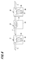
- FIG. 1st Embodiment It is a figure which shows schematic structure of the manufacturing apparatus of the transparent electrode of 1st Embodiment. It is a schematic block diagram of the transparent electrode produced with the manufacturing apparatus shown in FIG. It is a figure which shows schematic structure of the manufacturing apparatus of the transparent electrode of the modification of 1st Embodiment. It is a figure which shows schematic structure of the manufacturing apparatus of the transparent electrode of 2nd Embodiment. It is a schematic block diagram of the transparent electrode produced with the manufacturing apparatus shown in FIG. It is a figure which shows schematic structure of the manufacturing apparatus of the transparent electrode of the modification of 2nd Embodiment. It is a figure which shows schematic structure of the manufacturing apparatus of the organic EL element of 3rd Embodiment.
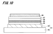
- FIG. 3 is a diagram showing a schematic configuration of a bottom emission type organic EL element produced in Example 2.
- Transparent electrode manufacturing apparatus first embodiment
- Transparent electrode manufacturing apparatus second embodiment
- Electronic device manufacturing apparatus third embodiment
- Transparent electrode manufacturing apparatus (first embodiment)> A first embodiment of the present invention will be described.
- FIG. 1 schematic structure of the manufacturing apparatus of the transparent electrode of 1st Embodiment is shown.
- FIG. 2 shows a schematic configuration (cross-sectional view) of a transparent electrode manufactured by this manufacturing apparatus.
- the manufacturing apparatus 20 illustrated in FIG. 1 includes a holding member 21 for the transparent base material 11, a plasma processing unit 22, and a conductive layer forming unit 25.
- the transparent electrode 10 produced by the manufacturing apparatus 20 includes a transparent base material 11 and a conductive layer 12 formed on the transparent base material 11.
- the transparent substrate 11 is used as the transparent member on which the conductive layer 12 is formed.
- transparent means that the light transmittance at a wavelength of 550 nm is 50% or more.
- the manufacturing apparatus 20 is a continuous apparatus in which the plasma processing unit 22 and the conductive layer forming unit 25 are arranged as a series of adjacent apparatuses. For this reason, the transparent base material 11 has the structure conveyed from the plasma processing part 22 to the conductive layer formation part 25 continuously. Moreover, the conveyance part between the plasma process part 22 and the conductive layer formation part 25 does not have the open part to the outside so that the transparent base material 11 after a plasma process may not be exposed to air
- these structures and materials used in this manufacturing apparatus will be described.
- the holding member 21 has a configuration for supplying the transparent base material 11 into the manufacturing apparatus 20.
- the holding member 21 is also configured as a conveying means for moving the held transparent base material 11 in one direction.
- the transparent substrate 11 held by the holding member 21 is supplied to the plasma processing unit 22 downstream of the manufacturing process.
- the transparent base material 11 When using the elongate transparent base material 11 which has flexibility, as shown in FIG. 1, it can comprise from the two rolls which can wind up and unwind the holding member 21. As shown in FIG. Moreover, when using the transparent base material 11 which does not have a flexibility, the transparent base material 11 can be hold
- the transfer speed of the transparent substrate 11 in the movement direction x by the holding member 21 is v [m / s].
- the speed v is a speed at which the thickness of the conductive layer formed in the conductive layer forming unit 25 described later becomes 15 nm or less in the continuous manufacturing apparatus 20. For example, it is set depending on the supply amount and supply region of the conductive material in the conductive layer forming unit 25.
- the speed v is a relative moving speed between the transparent substrate 11 and a plasma processing unit 22 and a conductive layer forming unit 25 described later.
- Transparent substrate examples of the transparent substrate 11 include, but are not limited to, glass and plastic.
- transparent substrate 11 glass, quartz, or a transparent resin film is preferably used.
- the glass examples include silica glass, soda lime silica glass, lead glass, borosilicate glass, and alkali-free glass. From the viewpoint of adhesion, durability, and smoothness, the surface of these glass materials is subjected to physical treatment such as polishing as necessary, or a coating made of an inorganic or organic material, or a combination of these coatings. A hybrid coating is formed.
- polyesters such as polyethylene terephthalate (PET) and polyethylene naphthalate (PEN), polyethylene, polypropylene, cellophane, cellulose diacetate, cellulose triacetate (TAC), cellulose acetate butyrate, cellulose acetate propionate ( CAP), cellulose esters such as cellulose acetate phthalate, cellulose nitrate or derivatives thereof, polyvinylidene chloride, polyvinyl alcohol, polyethylene vinyl alcohol, syndiotactic polystyrene, polycarbonate, norbornene resin, polymethylpentene, polyether ketone, polyimide , Polyethersulfone (PES), polyphenylene sulfide, polysulfone , Polyetherimide, polyetherketoneimide, polyamide, fluororesin, nylon, polymethylmethacrylate, acrylic or polyarylates, cyclone resins such as Arton (trade name, manufactured by JSR) or Appel (trade name
- a film made of an inorganic material or an organic material or a hybrid film combining these films may be formed on the surface of the resin film.
- Such coatings and hybrid coatings have a water vapor transmission rate (25 ⁇ 0.5 ° C., relative humidity 90 ⁇ 2% RH) of 0.01 g / (measured by a method in accordance with JIS-K-7129-1992. m 2 ⁇ 24 hours) or less of a barrier film (also referred to as a barrier film or the like) is preferable.
- the oxygen permeability measured by the method according to JIS-K-7126-1987 is 10 ⁇ 3 ml / (m 2 ⁇ 24 hours ⁇ atm) or less, and the water vapor permeability is 10 ⁇ 5 g / (m (2 ⁇ 24 hours) or less is preferable.
- the material for forming the barrier film as described above may be any material that has a function of suppressing intrusion of elements that cause deterioration of elements such as moisture and oxygen.
- silicon oxide, silicon dioxide, silicon nitride, or the like is used. be able to.
- the method for forming the barrier film is not particularly limited.
- the vacuum deposition method, the sputtering method, the reactive sputtering method, the molecular beam epitaxy method, the cluster ion beam method, the ion plating method, the plasma polymerization method, the atmospheric pressure plasma weighting can be used, but an atmospheric pressure plasma polymerization method described in JP-A No. 2004-68143 is particularly preferable.
- a known plasma processing apparatus can be used as the plasma processing unit 22.
- a vacuum chamber 23 serving as a processing chamber for performing plasma processing
- an exhaust unit for decompressing the vacuum chamber 23
- a gas supply unit for supplying a processing gas for plasma processing
- the vacuum chamber 23 It comprises a plasma generating unit 24 for generating plasma therein.
- the surface treatment of the transparent substrate 11 is performed by the plasma generated in the vacuum chamber 23.
- the surface treatment contaminants on the surface of the transparent substrate 11 are removed.
- the surface of the transparent substrate 11 is sputtered by the plasma, and the surface of the transparent substrate 11 becomes unstable.
- the surface of the transparent substrate 11 is modified by plasma.
- the plasma processing in the plasma processing unit 22 can be performed by a generally known method by appropriately optimizing. For example, it is preferable to use RF plasma.
- a gas containing oxygen atoms such as oxygen and nitrogen oxide, and an inert gas such as nitrogen and Ar can be used. Moreover, you may use multiple types of gas from an oxygen atom and an inert gas.
- the pressure of the processing gas is preferably about 0.1 to 2 Pa.
- ICP Inductive Coupled Plasma
- CCP Capacitive Coupled Plasma
- the high frequency applied to the plasma generator is generally a high frequency power of about 13.56 MHz and a power of about 0.1 to 5 kWh.
- the frequency and power that can generate plasma are limited to these. Not.
- a known film forming apparatus such as a known vapor deposition apparatus or sputtering apparatus can be used.
- an EB vapor deposition apparatus or a resistance heating vapor deposition apparatus can be used.
- a vacuum chamber 26 serving as a processing chamber for forming the conductive layer 12
- a supply unit 27 that supplies a conductive material 28 that constitutes the conductive layer 12
- an exhaust unit (not shown) that decompresses the vacuum chamber 26, and
- a film thickness measuring device not shown.
- the supply unit 27 is disposed on the main surface side of the transparent base material 11 conveyed by the holding member 21 and supplies the conductive material 28 toward the main surface of the transparent base material 11.
- the supply unit 27 is fixed in the vacuum chamber 26 and is provided across the width direction of the transparent substrate 11, which is a direction orthogonal to the moving direction x on the main surface of the transparent substrate 11.
- the supply part 27 is a structure for forming the conductive layer 12 on the main surface of the transparent substrate 11 conveyed by the holding member 21.
- the supply unit 27 includes, for example, a so-called heating boat for vapor deposition and a heating unit for the boat. By heating the conductive material 28 housed in the boat, the conductive material 28 can be gasified and supplied to the main surface of the transparent substrate 11.
- the transparent electrode manufactured by the manufacturing apparatus 20 has a thickness of the conductive layer 12 as thin as 15 nm at the maximum, it is important to control the thickness of the conductive layer 12 in the conductive layer forming portion 25.
- a crystal resonator is used as a film thickness measuring apparatus for measuring a film thickness during film formation.
- the conductive layer forming unit 25 has a problem in controlling the thickness of the conductive layer 12 and uniformity of the thickness in the plane of the conductive layer 12. It becomes. For this reason, the conductive layer forming unit 25 needs to be configured to be able to precisely control the thickness of the conductive layer 12.
- a plurality of film thickness measuring devices are installed in the conductive layer forming unit 25. Then, using a plurality of film thickness measuring devices, the film thickness is measured at a plurality of locations in the conductive layer forming portion 25, and the surface of the conductive layer 12 is checked by confirming this measured value and finely adjusting the in-plane distribution. The thickness uniformity can be improved.
- At least two film thickness measuring devices are installed in the conductive layer forming unit 25 on the transparent base material 11 side with respect to the supply unit 27 of the conductive material 28.
- by setting the height from the vapor deposition source to the film thickness measuring device to be the same and at a different distance from the vapor deposition source it is possible to control the thickness of the conductive layer forming unit 25 with high accuracy.
- a film thickness measuring device not only in the vicinity of the transparent substrate 11 but also in a portion close to the supply unit 27 serving as a deposition source of the conductive material 28.
- a film thickness measuring device is also installed in a portion near the supply unit 27, and the conductive layer 12 can be formed while performing control with higher accuracy by confirming the measured value and finely adjusting the supply unit 27. .
- a sputtering apparatus such as a DC sputtering apparatus in which the kinetic energy of the conductive material 28 that is sputtered into particles and flying in the vacuum is small.
- a DC sputtering apparatus In a state where the kinetic energy is low, such as a DC sputtering apparatus, the diffusion length of the particles of the conductive material 28 colliding with the surface of the transparent substrate 11 is short, and a uniform conductive layer 12 is formed on the surface of the transparent substrate 11. Easy to be.
- This also applies to the above-described EB vapor deposition apparatus and resistance heating vapor deposition apparatus. In these vapor deposition apparatuses, since the kinetic energy of particles is originally low, a uniform conductive layer 12 is easily formed on the surface of the transparent substrate 11.
- the conductive layer forming portion 25 is not limited to the above method as long as the conductive layer forming portion 25 can be formed to be thin and uniform, and other forming apparatuses can be applied.
- the conductive layer 12 In the transparent electrode 10, the conductive layer 12 needs to be formed of a translucent conductive material.
- the conductive layer 12 is, for example, a layer composed mainly of silver and is composed of silver or an alloy composed mainly of silver.
- an alloy mainly composed of silver (Ag) constituting the conductive layer 12 is silver magnesium (AgMg), silver copper (AgCu), silver palladium (AgPd), silver palladium copper (AgPdCu), silver indium (AgIn). , AgAu and the like.
- the conductive layer 12 as described above may have a structure in which silver or an alloy layer mainly composed of silver is divided into a plurality of layers as necessary.
- the conductive layer 12 preferably has a thickness in the range of 4 to 15 nm.
- the thickness of 15 nm or less, particularly 12 nm or less, is preferable because the absorption component and the reflection component of the conductive layer 12 are kept low and the light transmittance of the transparent electrode 10 is maintained.
- the electroconductivity of the conductive layer 12 is ensured by thickness being 4 nm or more.
- the upper portion of the conductive layer 12 may be covered with a protective film, or another conductive material may be laminated.
- the protective film and the conductive layer have light transmittance so that the light transmittance of the transparent electrode 10 is not impaired.
- the conductive layer 12 may have a configuration other than that containing silver as a main component. For example, you may use various transparent conductive substances, such as another metal, an alloy, ITO, a zinc oxide, a tin oxide.
- the conductive layer forming unit 25 is disposed downstream of the plasma processing unit 23 in the moving direction x of the transparent substrate 11.
- the conductive layer 12 is formed without exposing the surface of the transparent substrate 11 subjected to the plasma treatment to the atmosphere after the surface of the transparent substrate 11 is subjected to the plasma treatment.
- the conductive layer forming unit 25 is disposed at a predetermined interval d [m] between the conductive layer forming unit 25 and the plasma processing unit 22.
- This interval d is such that the interval from the end of the plasma treatment of the transparent substrate 11 to the start of the formation of the conductive layer 12 is within 5 minutes with respect to a predetermined position of the moving transparent substrate 11.
- This interval d is determined by the interval between the region where the plasma processing is performed in the plasma processing unit 22 (plasma processing region) and the region where the conductive layer 12 is formed in the conductive layer forming unit 25 (conductive layer forming region).
- the This interval d is expressed as follows.
- the speed v [m / s] of the movement of the transparent substrate 11 in the moving direction x, Sa is the plasma processing region in the vacuum chamber 23 of the plasma processing unit 22, and the conductive material 28 is supplied from the supply unit 27 to the conductive layer forming unit 25.
- the supplied conductive layer forming region is Sb.
- the distance between the end of the plasma processing region Sa and the start point of the conductive layer forming region Sb is d1 [m].
- the distance d [m] between the plasma processing unit 22 and the conductive layer forming unit 25 is set so that d1 ⁇ v ⁇ 300.
- the manufacturing apparatus 20 By using the manufacturing apparatus 20 as described above, it is possible to produce the transparent electrode 10 in which the main surface of the transparent substrate 11 is plasma-treated and the conductive layer 12 is formed on the treated surface.
- a mask is opposingly arranged on the main surface of the transparent base material 11 conveyed by the holding member 21, and it is the same direction. It can produce by transferring to.
- the conductive layer can be formed without exposing the treated surface to the atmosphere.
- the conductive layer can be densified by removing contaminants on the surface.
- the surface of the transparent member becomes unstable due to the sputtering effect of the plasma treatment.
- the number of growth nuclei generated first in the formation of the conductive layer increases.
- the surface of the transparent member is presumed to be caused by not only surface cleaning but also shape instability due to generation of defects and energy level instability due to the sputtering effect of plasma. It is presumed that defects generated on the surface of the transparent member by plasma sputtering are defects that can be corrected in a self-aligning manner over time. Moreover, it is estimated that the part sputtered
- the defect of the transparent member is repaired by the interaction with silver. For this reason, by supplying silver before defects are repaired by self-alignment, minute silver particles for correcting local defects in the transparent member are uniformly formed over the entire surface of the transparent member. It is thought.
- the energy level of the surface of the transparent member is reduced by interaction with silver constituting the conductive layer. It is presumed that it can be returned to a stable state.
- the surface of the transparent member becomes stable due to the action of defects in the transparent member and active substances such as oxygen and water. For this reason, it is necessary to form a conductive layer without being exposed to the atmosphere after the plasma treatment.
- the surface defects and energy state of the transparent member are stabilized in a self-aligning manner, so the conductive layer is formed before the unstable state caused by the plasma treatment is stabilized. .
- the above effect becomes remarkable.
- the surface becomes stable due to self-alignment over time.
- the number of growth nuclei formed on the surface is reduced.
- a transparent electrode having sufficient conductivity and light transmissivity is produced. Can do.
- FIG. 3 shows a configuration of a single wafer manufacturing apparatus as a modification of the manufacturing apparatus of the first embodiment.
- the transparent electrode manufacturing apparatus of the present example includes a holding part for a transparent substrate 11 (not shown), a plasma processing part 22, and a conductive layer forming part 25.
- the manufacturing apparatus of this example only the conveyance method of the above-mentioned 1st Embodiment and the transparent base material 11 differs, and each structure of the plasma processing part 22 and the conductive layer formation part 25 which comprise a manufacturing apparatus is the above-mentioned. This is the same as the first embodiment.
- the transparent electrode manufactured with the manufacturing apparatus of this example is the same structure as the transparent electrode 10 of the structure shown in FIG. 2 similarly to the above-mentioned 1st Embodiment.
- the distance d [m] between the plasma processing unit 22 and the conductive layer forming unit 25 is not particularly limited. What is necessary is just the structure between the plasma process part 22 and the conductive layer formation part 25 if the surface of the transparent base material 11 is not exposed to air
- FIG. 4 the schematic block diagram of the manufacturing apparatus of the transparent electrode of 2nd Embodiment is shown.
- FIG. 5 shows a schematic configuration diagram (cross-sectional view) of a transparent electrode manufactured by this manufacturing apparatus.
- the detailed description which overlaps about the component similar to 1st Embodiment is abbreviate
- the manufacturing apparatus 40 shown in FIG. 4 includes a holding member 21 for the transparent substrate 11, a high refractive index layer forming unit 31, a plasma processing unit 22, and a conductive layer forming unit 25.
- the transparent electrode 30 produced by the manufacturing apparatus 40 includes a transparent base material 11, a high refractive index layer 13 formed on the transparent base material 11, and a high refractive index layer 13.
- the formed conductive layer 12 is provided.
- the transparent base material 11 and the high refractive index layer 13 provided on the transparent base material 11 are used as the transparent member on which the conductive layer is formed.
- the manufacturing apparatus 40 is a continuous apparatus in which the high refractive index layer forming unit 31, the plasma processing unit 22, and the conductive layer forming unit 25 are arranged as a series of adjacent devices. For this reason, the transparent base material 11 has the structure conveyed continuously from the high refractive index layer formation part 31 to the conductive layer formation part 25.
- FIG. 1 A diagrammatic representation of the manufacturing apparatus 40.
- the conveyance unit between the plasma processing unit 22 and the conductive layer forming unit 25 does not have an open part to the outside so that the transparent substrate 11 after the plasma processing is not exposed to the atmosphere.
- the transport unit between the high refractive index layer forming unit 31 and the plasma processing unit 22 has an open part to the outside. Not done. That is, the manufacturing apparatus 40 has a configuration closed at least from the high refractive index layer forming unit 31 to the conductive layer forming unit 25.
- the holding member 21, the plasma processing unit 22, and the conductive layer forming unit 25 have the same configuration as the manufacturing apparatus of the first embodiment described above.
- the transparent electrode 30 the transparent base material 11 and the conductive layer 12 can use the structure similar to the structure demonstrated with the manufacturing apparatus of the above-mentioned 1st Embodiment. For this reason, description of the same configurations as those of the first embodiment is omitted.
- High refractive index layer forming part (Constitution)
- a known film forming apparatus such as a known vapor deposition apparatus or sputtering apparatus can be used.
- an electron beam evaporation apparatus can be used.
- the high refractive index layer forming unit 31 supplies, for example, a vacuum chamber 32 serving as a processing chamber for forming the high refractive index layer 13 and a high refractive index material 34 such as a metal oxide constituting the high refractive index layer 13.
- the supply unit 33 and an exhaust unit (not shown) for decompressing the vacuum chamber 26 are configured.
- the supply unit 33 is disposed on the main surface side of the transparent base material 11 transferred by the holding member 21 and supplies the high refractive index material 34 toward the main surface of the transparent base material 11.
- the supply unit 33 is fixed in the vacuum chamber 32 and is provided across the width direction of the transparent substrate 11, which is a direction orthogonal to the moving direction x on the main surface of the transparent substrate 11.
- the supply part 33 is a structure for forming the high refractive index layer 13 on the main surface of the transparent substrate 11 transferred by the holding member 21.
- the supply unit 33 includes, for example, an electron beam evaporation boat and an electron gun that irradiates the high refractive index material 34 housed in the boat with an electron beam. By irradiating the high refractive index material 34 accommodated in the boat with an electron beam, the high refractive index material 34 can be gasified and supplied to the main surface of the transparent substrate 11.
- the high refractive index layer 13 needs to have a refractive index larger than that of the transparent substrate 11, and is preferably a layer having a refractive index (n) of 1.9 or more at a wavelength of 550 nm. Particularly preferred is a layer having a refractive index (n) of 2.0 or more at a wavelength of 550 nm.
- a metal oxide is used for such a high refractive index layer 13.
- the high refractive index layer 13 is preferably formed with a thickness of 10 to 100 nm. In particular, the thickness of about 20 nm is effective for suppressing reflection of the transparent electrode 30.
- the high refractive index layer forming part 31, the plasma processing part 22, and the conductive layer forming part 25 are arranged in this order from the holding member 21 toward the downstream side in the moving direction x of the transparent base material 11.
- the process from the formation of the high refractive index layer 13 to the formation of the conductive layer 12 is performed without exposing the transparent substrate 11 to the atmosphere.
- the conductive layer 12 is formed without exposing the surface subjected to the plasma treatment to the atmosphere.
- the high refractive index layer 13 is formed on the transparent substrate 11.
- the surface of the formed high refractive index layer 13 is subjected to plasma processing. Contaminants on the surface of the high refractive index layer 13 are removed by plasma treatment. Further, the surface of the high refractive index layer 13 is sputtered by the plasma, and the surface of the high refractive index layer 13 is made unstable. Further, the surface of the high refractive index layer 13 is modified by plasma treatment.
- the conductive layer 12 is formed in the conductive layer forming portion 25.
- the conductive layer forming unit 25 is arranged with a predetermined distance d [m] between the conductive layer forming unit 25 and the plasma processing unit 22. This interval d is such that the interval from the end of the plasma treatment of the transparent substrate 11 to the start of the formation of the conductive layer 12 is within 5 minutes with respect to a predetermined position of the moving transparent substrate 11. Set to.
- This interval d is determined by the interval between the region where the plasma processing is performed in the plasma processing unit 22 (plasma processing region) and the region where the conductive layer 12 is formed in the conductive layer forming unit 25 (conductive layer forming region).
- the This interval d is expressed as follows.
- the formation region is Sb.
- the distance between the end of the plasma processing region Sa and the start point of the conductive layer forming region Sb is d1 [m].
- the distance d [m] between the plasma processing unit 22 and the conductive layer forming unit 25 is set so that d1 ⁇ v ⁇ 300.
- the high refractive index layer 13 is formed on the main surface of the transparent substrate 11, the surface of the high refractive index layer 13 is plasma-treated, and the conductive layer is formed on the processed surface.
- the transparent electrode 30 in which 12 is formed can be produced.
- it can produce by arrange
- the transparent member includes not only a transparent base material such as glass or resin, but also a layer that adjusts an optical action such as a high refractive index layer made of a metal oxide or the like. Can also be applied.
- the structure of the transparent member on which the conductive layer is formed is not particularly limited as long as the surface on which the conductive layer is formed can be subjected to plasma treatment.
- a conductive layer can be formed, without exposing this process surface to air
- the conductive layer can be densified by removing contaminants on the surface.
- the surface of the transparent member becomes uneasy due to the sputtering effect of the plasma treatment.
- the formation of the conductive layer is stabilized.
- the diffusion distance of the conductive material is reduced and aggregation is suppressed.
- conductive materials that are likely to be isolated like islands due to the growth of the nuclear growth type can be obtained by the growth of the single layer growth type (Frank-van der Merwe: FM type). Will be formed.
- FIG. 6 shows a configuration of a single wafer manufacturing apparatus as a modification of the manufacturing apparatus of the second embodiment.
- the transparent electrode manufacturing apparatus of this example includes a holding part for a transparent base material 11 (not shown), a high refractive index layer forming part 31, a plasma processing part 22, and a conductive layer forming part 25. Is done.
- the manufacturing apparatus of this example only the conveyance method of the transparent substrate 11 is different from the above-described second embodiment, and the high refractive index layer forming unit 31, the plasma processing unit 22, and the conductive layer forming which constitute the manufacturing apparatus.
- Each structure of the part 25 is the same as that of the above-mentioned 2nd Embodiment.
- the transparent electrode manufactured with the manufacturing apparatus of this example is the same structure as the transparent electrode 30 of the structure shown in FIG. 4 similarly to the above-mentioned 2nd Embodiment.
- the distance d [m] between the plasma processing unit 22 and the conductive layer forming unit 25 is not particularly limited. What is necessary is just the structure between the plasma process part 22 and the conductive layer formation part 25 if the surface of the transparent base material 11 is not exposed to air
- the third embodiment describes an apparatus for manufacturing a bottom emission type organic electroluminescence element (organic EL element) using the transparent electrode of the second embodiment described above as an example of an apparatus for manufacturing an electronic device using a transparent electrode. To do.
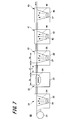
- FIG. 7 the surface block diagram of the manufacturing apparatus of the organic EL element of this embodiment is shown.
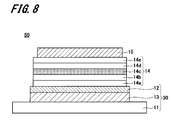
- FIG. 8 shows a schematic configuration diagram (cross-sectional view) of an organic EL element manufactured by this manufacturing apparatus.
- 7 includes a holding member 21, a high refractive index layer forming unit 31, a plasma processing unit 22, a conductive layer forming unit 25, a light emitting functional layer forming unit 41, and a counter electrode forming unit. 45.
- the organic EL element 50 manufactured by the manufacturing apparatus 60 is provided on the transparent electrode 30 including the transparent base material 11, the high refractive index layer 13, and the conductive layer 12.
- the light emitting functional layer 14 and the counter electrode 15 provided on the light emitting functional layer 14 are provided.
- the conductive layer 12 functions as an anode (that is, an anode)
- the counter electrode 15 functions as a cathode (that is, a cathode).
- the light emitting functional layer 14 has a structure in which a hole injection layer 14a / a hole transport layer 14b / a light emission layer 14c / an electron transport layer 14d / an electron injection layer 14e are stacked in this order from the conductive layer 12 side which is an anode.
- the manufacturing apparatus 60 is a continuous apparatus in which the high refractive index layer forming unit 31 to the counter electrode forming unit 45 are arranged as a series of devices. For this reason, the transparent base material 11 has the structure conveyed continuously from the high refractive index layer formation part 31 to the counter electrode formation part 45. FIG. Moreover, the conveyance part between the plasma process part 22 and the conductive layer formation part 25 does not have the open part to the outside so that the transparent base material 11 after a plasma process may not be exposed to air
- the holding member 21, the high refractive index layer forming unit 31, the plasma processing unit 22, and the conductive layer forming unit 25 have the same configuration as the manufacturing apparatus of the second embodiment described above.
- the organic EL element 50, the transparent substrate 11, the high refractive index layer 13, and the conductive layer 12 can have the same configuration as that described in the manufacturing apparatus of the second embodiment. For this reason, description of the same configuration as those of the second embodiment is omitted.
- the light emitting functional layer forming part 41 is composed of a plurality of forming parts in accordance with the number of layers constituting the light emitting functional layer.
- the light emitting functional layer 14 is composed of five layers of a hole injection layer 14a / a hole transport layer 14b / a light emission layer 14c / an electron transport layer 14d / an electron injection layer 14e.
- the light emitting functional layer forming part 41 is composed of five forming parts corresponding to the five layers.
- FIG. 7 only one forming portion is representatively shown from a plurality of forming portions constituting the light emitting functional layer forming portion 41.
- the light emitting functional layer forming unit 41 As the light emitting functional layer forming unit 41, a known film forming apparatus such as a known vapor deposition apparatus or sputtering apparatus can be used. For example, a vacuum deposition apparatus can be used.
- the light emitting functional layer forming unit 41 supplies, for example, a vacuum chamber 42 serving as a processing chamber for forming each layer constituting the light emitting functional layer forming unit 41, and an organic material 44 of each layer constituting the light emitting functional layer forming unit 41.
- a supply unit 43 and an exhaust unit (not shown) for decompressing the vacuum chamber 42 are included.
- the supply part 43 is arrange
- the organic material 44 constituting the layer 14b / light emitting layer 14c / electron transport layer 14d / electron injection layer 14e) is supplied.
- the supply unit 43 is fixed in the vacuum chamber 42 and is provided across the width direction of the transparent substrate 11, which is a direction orthogonal to the moving direction x on the main surface of the transparent substrate 11.
- the supply unit 43 is configured to form the light emitting functional layer 14 on the conductive layer 12 on the main surface side of the transparent substrate 11 transferred by the holding member 21.
- the supply unit 43 includes, for example, a so-called heating boat for vapor deposition film formation and a heating unit for the boat. By heating the organic material 44 housed inside the boat, the organic material 44 can be gasified and supplied onto the conductive layer 12 on the main surface side of the transparent substrate 11.
- Counter electrode forming part As the counter electrode formation part 45, a well-known film-forming apparatus, such as a well-known vapor deposition apparatus and sputtering apparatus, can be used. For example, a vacuum deposition apparatus can be used.
- the counter electrode forming portion 45 may have the same configuration as the conductive layer forming portion 25 described above.
- the counter electrode forming unit 45 includes, for example, a vacuum chamber 46 serving as a processing chamber for forming the counter electrode 15, a supply unit 47 that supplies a conductive material 48 that constitutes the counter electrode 15, and the vacuum chamber 46 is decompressed.
- the exhaust part (illustration omitted) etc. to be performed are comprised.
- the supply unit 47 is disposed on the main surface side of the transparent base material 11 transferred by the holding member 21 and supplies the conductive material 48 toward the main surface of the transparent base material 11.
- the supply unit 47 is fixed in the vacuum chamber 46 and is provided across the width direction of the transparent substrate 11, which is a direction orthogonal to the moving direction x on the main surface of the transparent substrate 11.
- the supply part 47 is a structure for forming the counter electrode 15 on the main surface of the transparent base material 11 transferred by the holding member 21.
- the supply unit 47 includes, for example, a so-called heating boat for vapor deposition and a heating unit for the boat. By heating the conductive material 48 housed inside the boat, the conductive material 48 can be gasified and supplied to the main surface of the transparent substrate 11.
- the counter electrode forming part 45 may have the same configuration as the conductive layer forming part 25.
- the counter electrode 15 can be formed of a conductive material containing silver as a main component, similar to the conductive layer 12.
- the plasma processing part 22 can be inserted before the conductive layer forming part 25.
- the plasma processing part 22 can be inserted before the conductive layer forming part 25.
- a thin and uniform conductive layer 12 can be formed as in the first embodiment.
- the organic EL element 50 can be made into the double emission type which takes out the emitted light h also from the opposite side to the transparent base material 11, or a top emission type.
- the light emitting functional layer 14 is constituted by a hole injection layer 14a / hole transport layer 14b / light emission layer 14c / electron transport layer 14d / electron injection layer 14e.
- the hole injection layer 14a and the hole transport layer 14b may be provided as a hole transport / injection layer.
- the electron transport layer 14d and the electron injection layer 14e may be provided as an electron transport / injection layer.
- the electron injection layer 14e may be made of an inorganic material.
- the light emitting functional layer 14 may have a hole blocking layer, an electron blocking layer, or the like laminated as necessary.
- the light emitting layer 14c has each color light emitting layer for generating light emission in each wavelength region, and each of these color light emitting layers is laminated via a non-light emitting intermediate layer to form a light emitting layer unit. Also good.
- the intermediate layer may function as a hole blocking layer and an electron blocking layer. In such a configuration, only a portion where the light emitting functional layer 14 is sandwiched between the conductive layer 12 and the counter electrode 15 becomes a light emitting region in the organic EL element 50.
- the light emitting layer 14c used for the organic EL element 50 of this embodiment contains, for example, a phosphorescent light emitting compound as a light emitting material.
- the light emitting layer 14c is a layer that emits light by recombination of electrons injected from the electrode or the electron transport layer 14d and holes injected from the hole transport layer 14b, and the light emitting portion is the light emitting layer 14c. Even within the layer, it may be an interface with an adjacent layer in the light emitting layer 14c.
- the configuration of the light emitting layer 14c is not particularly limited as long as the included light emitting material satisfies the light emission requirements. Moreover, there may be a plurality of layers having the same emission spectrum and emission maximum wavelength. In this case, it is preferable to have a non-light emitting intermediate layer (not shown) between the light emitting layers 14c.
- the total thickness of the light emitting layer 14c is preferably in the range of 1 to 100 nm, and more preferably 1 to 30 nm because it can be driven at a lower voltage.
- the sum total of the thickness of the light emitting layer 14c is a thickness also including the said intermediate
- the thickness of each light emitting layer is preferably adjusted to a range of 1 to 50 nm, and more preferably adjusted to a range of 1 to 20 nm.
- the plurality of stacked light emitting layers correspond to the respective emission colors of blue, green, and red, there is no particular limitation on the relationship between the thicknesses of the blue, green, and red light emitting layers.
- the light emitting layer 14c as described above can be formed of a light emitting material or a host compound, which will be described later, by a known thin film forming method such as a vacuum evaporation method, a spin coating method, a casting method, an LB method, or an ink jet method.
- a known thin film forming method such as a vacuum evaporation method, a spin coating method, a casting method, an LB method, or an ink jet method.
- the light emitting layer 14c may be a mixture of a plurality of light emitting materials, or a phosphorescent light emitting material and a fluorescent light emitting material (also referred to as a fluorescent dopant or a fluorescent compound) may be mixed and used in the same light emitting layer 14c.
- the structure of the light emitting layer 14c preferably includes a host compound (also referred to as a light emitting host) and a light emitting material (also referred to as a light emitting dopant compound or a guest material) and emits light from the light emitting material.
- a host compound also referred to as a light emitting host
- a light emitting material also referred to as a light emitting dopant compound or a guest material
- the host compound contained in the light emitting layer 14c As the host compound contained in the light emitting layer 14c, a compound having a phosphorescence quantum yield of phosphorescence emission at room temperature (25 ° C.) of less than 0.1 is preferable. Furthermore, the compound whose phosphorescence quantum yield is less than 0.01 is preferable.
- the host compound preferably has a volume ratio in the layer of 50% or more among the compounds contained in the light emitting layer 14c.
- the host compound a known host compound may be used alone, or a plurality of types may be used. By using a plurality of types of host compounds, it is possible to adjust the movement of charges, and the organic EL element 50 can be made highly efficient. In addition, by using a plurality of kinds of light emitting materials described later, it is possible to mix different light emission, thereby obtaining an arbitrary light emission color.
- the host compound used may be a conventionally known low molecular compound, a high molecular compound having a repeating unit, or a low molecular compound having a polymerizable group such as a vinyl group or an epoxy group (evaporation polymerizable light emitting host). .
- Tg glass transition temperature
- the host compound applicable to the organic electroluminescence device include compounds H1 to H79 described in paragraphs [0163] to [0178] of JP2013-4245A.
- the compounds H1 to H79 described in paragraphs [0163] to [0178] of JP2013-4245 are incorporated in the present specification.
- Luminescent material examples of the light-emitting material that can be used for the organic EL element of the present embodiment include phosphorescent compounds (also referred to as phosphorescent compounds and phosphorescent materials).
- a phosphorescent compound is a compound in which light emission from an excited triplet is observed. Specifically, a phosphorescent compound emits phosphorescence at room temperature (25 ° C.), and a phosphorescence quantum yield of 0.01 at 25 ° C. Although defined as the above compounds, the preferred phosphorescence quantum yield is 0.1 or more.
- the phosphorescent quantum yield can be measured by the method described in Spectroscopic II, page 398 (1992 edition, Maruzen) of Experimental Chemistry Course 4 of the 4th edition. Although the phosphorescence quantum yield in a solution can be measured using various solvents, when the phosphorescent compound is used in this example, the phosphorescence quantum yield (0.01 or more) is achieved in any solvent. It only has to be done.
- phosphorescent compounds There are two types of light emission principles of phosphorescent compounds. One is that recombination of carriers occurs on the host compound to which carriers are transported to generate an excited state of the host compound, and this energy is transferred to the phosphorescent compound to obtain light emission from the phosphorescent compound.
- the other is a carrier trap type in which the phosphorescent compound becomes a carrier trap, and carriers are recombined on the phosphorescent compound to emit light from the phosphorescent compound. In either case, it is a condition that the excited state energy of the phosphorescent compound is lower than the excited state energy of the host compound.
- the phosphorescent compound can be appropriately selected from known materials used for the light emitting layer 14c of a general organic EL device, and preferably contains a metal of group 8 to 10 in the periodic table of elements. It is a complex compound. More preferred are iridium compounds, osmium compounds, platinum compounds (platinum complex compounds), and rare earth complexes, and most preferred are iridium compounds.
- At least one light emitting layer 14c may contain two or more phosphorescent compounds, and the concentration ratio of the phosphorescent compounds in the light emitting layer 14c is the same as that of the light emitting layer 14c. It may change in the thickness direction.
- the phosphorescent compound is preferably 0.1% by volume or more and less than 30% by volume with respect to the total amount of the light emitting layer 14c.
- Examples of phosphorescent compounds applicable to the organic EL element 50 include those represented by general formulas (4), (5), and (6) described in paragraphs [0185] to [0235] of JP2013-4245A.
- Preferred examples include the compounds represented and exemplary compounds.
- Ir-46, Ir-47, and Ir-48 are shown below.
- Compounds represented by general formula (4), general formula (5) and general formula (6) described in paragraphs [0185] to [0235] of JP2013-4245A and exemplified compounds (Pt-1 to Pt) -3, Os-1, Ir-1 to Ir-45) are incorporated herein.
- these phosphorescent compounds are contained in the light emitting layer 14c of the organic EL element 50 as a light emitting dopant, organic functions other than the light emitting layer 25c are included. It may be contained in the layer.
- phosphorescent compounds are, for example, OrganicOrLetters magazine vol.3 No.16 2579-2581 (2001), Inorganic Chemistry, Vol.30, No.8 1685-1687. (1991), J. Am. Chem. Soc., 123 4304 (2001), Inorganic Chemistry, Vol. 40, No. 7, 704 1704-1711 (2001), Inorganic Chemistry, Vol. 41 No. 12 3055-3066 (2002), New Journal of ⁇ Chemistry., 26261171 (2002), European Journal of Organic Chemistry, Vol.4 695-709 (2004), further described in these documents Can be synthesized by applying a method such as the reference.
- Fluorescent materials include coumarin dyes, pyran dyes, cyanine dyes, croconium dyes, squalium dyes, oxobenzanthracene dyes, fluorescein dyes, rhodamine dyes, pyrylium dyes, perylene dyes, stilbene dyes Examples thereof include dyes, polythiophene dyes, and rare earth complex phosphors.
- injection layer hole injection layer, electron injection layer
- the injection layer is a layer provided between the electrode and the light-emitting layer 14c in order to lower the driving voltage and improve the light emission luminance.
- the injection layer can be provided as necessary.
- the hole injection layer 14a is disposed between the anode and the light emitting layer 14c or the hole transport layer 14b, and the electron injection layer 14e is disposed between the cathode and the light emitting layer 14c or the electron transport layer 14d.
- the details of the hole injection layer 14a are also described in JP-A-9-45479, JP-A-9-260062, JP-A-8-288069 and the like.
- Specific examples thereof include phthalocyanine represented by copper phthalocyanine.
- Examples thereof include a layer, an oxide layer typified by vanadium oxide, an amorphous carbon layer, and a polymer layer using a conductive polymer such as polyaniline (emeraldine) or polythiophene.
- the details of the electron injection layer 14e are described in JP-A-6-325871, JP-A-9-17574, JP-A-10-74586, and the like, and specifically represented by strontium, aluminum and the like.
- Examples thereof include a metal layer, an alkali metal halide layer typified by potassium fluoride, an alkaline earth metal compound layer typified by magnesium fluoride, and an oxide layer typified by molybdenum oxide.
- the electron injection layer 14e is desirably a very thin layer, and its thickness is preferably in the range of 1 nm to 10 ⁇ m, although it depends on the material.
- the hole transport layer 14b is made of a hole transport material having a function of transporting holes, and in a broad sense, the hole injection layer 14a and the electron blocking layer are also included in the hole transport layer 14b.
- the hole transport layer 14b can be provided as a single layer or a plurality of layers.
- the hole transport material has any of hole injection or transport and electron barrier properties, and may be either organic or inorganic.
- triazole derivatives oxadiazole derivatives, imidazole derivatives, polyarylalkane derivatives, pyrazoline derivatives and pyrazolone derivatives, phenylenediamine derivatives, arylamine derivatives, amino-substituted chalcone derivatives, oxazole derivatives, styrylanthracene derivatives, fluorenone derivatives, hydrazone derivatives
- Examples thereof include stilbene derivatives, silazane derivatives, aniline copolymers, and conductive polymer oligomers, particularly thiophene oligomers.
- hole transport material those described above can be used, but it is preferable to use a porphyrin compound, an aromatic tertiary amine compound and a styrylamine compound, particularly an aromatic tertiary amine compound.
- aromatic tertiary amine compounds and styrylamine compounds include N, N, N ′, N′-tetraphenyl-4,4′-diaminophenyl; N, N′-diphenyl-N, N′— Bis (3-methylphenyl)-[1,1′-biphenyl] -4,4′-diamine (TPD); 2,2-bis (4-di-p-tolylaminophenyl) propane; 1,1-bis (4-di-p-tolylaminophenyl) cyclohexane; N, N, N ′, N′-tetra-p-tolyl-4,4′-diaminobiphenyl; 1,1-bis (4-di-p-tolyl) Aminophenyl) -4-phenylcyclohexane; bis (4-dimethylamino-2-methylphenyl) phenylmethane; bis (4-di-p-tolylaminoph
- a polymer material in which these materials are introduced into a polymer chain or these materials are used as a polymer main chain can also be used.
- inorganic compounds such as p-type-Si and p-type-SiC can also be used as the hole injection material and the hole transport material.
- p-type hole transport materials as described in JP-A-11-251067, J. Huang et al., Applied Physics Letters, 80 (2002), p. 139 can be used. . These materials are preferably used because a highly efficient light-emitting element can be obtained.
- the hole transport layer 14b is formed by thinning the hole transport material by a known method such as a vacuum deposition method, a spin coating method, a casting method, a printing method including an ink jet method, or an LB method. be able to.
- the thickness of the hole transport layer 14b is not particularly limited, but is usually about 5 nm to 5 ⁇ m, preferably 5 to 200 nm.
- the hole transport layer 14b may have a single layer structure composed of one or more of the above materials.
- the electron transport layer 14d is made of a material having a function of transporting electrons. In a broad sense, the electron transport layer 14e and a hole blocking layer (not shown) are also included in the electron transport layer 14d.
- the electron transport layer 14d can be provided as a single layer structure or a stacked structure of a plurality of layers.
- an electron transport material (also serving as a hole blocking material) constituting the layer portion adjacent to the light emitting layer 14c in the electron transport layer 14d having a single layer structure and the electron transport layer 14d having a multilayer structure
- electrons injected from the cathode are used. What is necessary is just to have the function transmitted to the light emitting layer 14c.
- Such a material can be arbitrarily selected from conventionally known compounds. Examples include nitro-substituted fluorene derivatives, diphenylquinone derivatives, thiopyran dioxide derivatives, carbodiimides, fluorenylidenemethane derivatives, anthraquinodimethane, anthrone derivatives, and oxadiazole derivatives.
- a thiadiazole derivative in which the oxygen atom of the oxadiazole ring is substituted with a sulfur atom, and a quinoxaline derivative having a quinoxaline ring known as an electron-withdrawing group are also used as the material for the electron transport layer 14d.
- a polymer material in which these materials are introduced into a polymer chain or these materials are used as a polymer main chain can also be used.
- metal complexes of 8-quinolinol derivatives such as tris (8-quinolinol) aluminum (Alq3), tris (5,7-dichloro-8-quinolinol) aluminum, tris (5,7-dibromo-8-quinolinol) aluminum Tris (2-methyl-8-quinolinol) aluminum, tris (5-methyl-8-quinolinol) aluminum, bis (8-quinolinol) zinc (Znq), and the like, and the central metals of these metal complexes are In, Mg, A metal complex replaced with Cu, Ca, Sn, Ga, or Pb can also be used as the material of the electron transport layer 14d.
- metal-free or metal phthalocyanine or the terminal thereof is substituted with an alkyl group or a sulfonic acid group, it can be preferably used as a material for the electron transport layer 14d.
- a distyrylpyrazine derivative exemplified also as a material of the light emitting layer 14c can be used as a material of the electron transport layer 14d, and is similar to the hole injection layer 14a and the hole transport layer 14b, n-type-Si, n-type.
- An inorganic semiconductor such as -SiC can also be used as the material of the electron transport layer 14d.
- the electron transport layer 14d can be formed by thinning the above material by a known method such as a vacuum deposition method, a spin coating method, a casting method, a printing method including an ink jet method, or an LB method.
- the thickness of the electron transport layer 14d is not particularly limited, but is usually about 5 nm to 5 ⁇ m, preferably 5 to 200 nm.
- the electron transport layer 14d may have a single layer structure composed of one or more of the above materials.
- the electron transport layer 14d can be doped with impurities to increase the n property. Examples thereof include JP-A-4-297076, JP-A-10-270172, JP-A-2000-196140, 2001-102175, J. Appl. Phys., 95, 5773 (2004), etc. What has been described. Furthermore, it is preferable that the electron transport layer 14d contains potassium, a potassium compound, or the like. As the potassium compound, for example, potassium fluoride can be used. As described above, when the n property of the electron transport layer 14d is increased, an element with lower power consumption can be manufactured.
- Examples of the material (electron transporting compound) of the electron transport layer 14d include, for example, the general formula (1), the general formula (2), and the general formula (2) described in paragraphs [0057] to [0148] of JP2013-4245A.
- the compound represented by the general formula (3) is preferably used, and Exemplified Compounds 1-111 can be used. Further, as other exemplary compounds, compounds 112 to 134 are shown below.
- the compounds represented by general formula (1), general formula (2), and general formula (3) described in paragraphs [0057] to [0148] of JP2013-4245 are incorporated in the present specification.
- Blocking layer hole blocking layer, electron blocking layer
- the blocking layer is provided as necessary in addition to the basic constituent layer of the organic compound thin film. For example, it is described in JP-A Nos. 11-204258 and 11-204359, and “Organic EL elements and the forefront of industrialization (published by NTT Corporation on November 30, 1998)” on page 237. There is a hole blocking (hole blocking) layer.
- the hole blocking layer has a function of the electron transport layer 14d in a broad sense.
- the hole blocking layer is made of a hole blocking material that has a function of transporting electrons but has a very small ability to transport holes, and recombines electrons and holes by blocking holes while transporting electrons. Probability can be improved.
- the structure of the electron carrying layer 14d mentioned later can be used as a hole-blocking layer as needed.
- the hole blocking layer is preferably provided adjacent to the light emitting layer 14c.
- the electron blocking layer has a function of the hole transport layer 14b in a broad sense.
- the electron blocking layer is made of a material that has a function of transporting holes but has a very small ability to transport electrons, and improves the probability of recombination of electrons and holes by blocking electrons while transporting holes. be able to.
- the structure of the positive hole transport layer 14b mentioned later can be used as an electron blocking layer as needed.
- the thickness of the blocking layer is preferably 3 to 100 nm, and more preferably 5 to 30 nm.
- the high refractive index layer 13 is formed on the transparent substrate 11 in the high refractive index layer forming part 31. Subsequently, in the plasma processing unit 22, the surface of the formed high refractive index layer 13 is subjected to plasma processing.
- the contaminants on the surface of the high refractive index layer 13 are removed by plasma treatment. Further, the surface of the high refractive index layer 13 is sputtered by the plasma, and the surface of the high refractive index layer 13 is made unstable. Further, the surface of the high refractive index layer 13 is modified by plasma treatment.
- the conductive layer 12 is formed in the conductive layer forming portion 25.
- the conductive layer forming unit 25 is arranged with a predetermined distance d [m] between the conductive layer forming unit 25 and the plasma processing unit 22. This interval d is such that the interval from the end of the plasma treatment of the transparent substrate 11 to the start of the formation of the conductive layer 12 is within 5 minutes with respect to a predetermined position of the moving transparent substrate 11. Set to.
- This interval d is determined by the interval between the region where the plasma processing is performed in the plasma processing unit 22 (plasma processing region) and the region where the conductive layer 12 is formed in the conductive layer forming unit 25 (conductive layer forming region).
- the This interval d is expressed as follows.
- the formation region is Sb.
- the distance between the end of the plasma processing region Sa and the start point of the conductive layer forming region Sb is d1 [m].
- the distance d [m] between the plasma processing unit 22 and the conductive layer forming unit 25 is set so that d1 ⁇ v ⁇ 300.
- the light emitting functional layer forming unit 41 forms the light emitting functional layer 14 on the conductive layer 12.
- the formation of these layers varies depending on the type of compound used, but generally, the boat heating temperature is 50 ° C. to 450 ° C., the degree of vacuum is 10 ⁇ 6 Pa to 10 ⁇ 2 Pa, and the deposition rate is 0.01 nm / second to 50 nm / second.
- the deposition conditions are appropriately selected within the range of the substrate temperature ⁇ 50 ° C. to 300 ° C. and the film thickness of 0.1 ⁇ m to 5 ⁇ m.
- these layers can also be formed by a pin coat method, a cast method, an ink jet method, a printing method, or the like. Different Keisei methods may be applied for each layer.
- an apparatus suitable for each manufacturing method may be used as the light emitting functional layer forming portion 41.
- the counter electrode 15 is formed in the counter electrode forming portion 45.
- the counter electrode 15 is formed by an appropriate film forming method such as an evaporation method or a sputtering method.
- the counter electrode 15 is patterned in a shape in which a terminal portion is drawn from the upper side of the light emitting functional layer 14 to the periphery of the transparent substrate 11 while maintaining the insulating state with respect to the conductive layer 12 by the light emitting functional layer 14.
- the high refractive index layer 13 is formed on the main surface of the transparent substrate 11, the surface of the high refractive index layer 13 is subjected to plasma treatment, and a conductive layer is formed on the processed surface.
- the transparent electrode 30 in which 12 is formed can be produced.
- the organic EL element 50 in which the light emitting functional layer 14 and the counter electrode 15 are formed on the conductive layer 12 of the transparent electrode 30 can be produced.
- it can produce by arrange
- FIG. 9 shows a configuration of a manufacturing apparatus for a single wafer type organic EL element as a modification of the manufacturing apparatus of the third embodiment.
- the organic EL element manufacturing apparatus of this example includes a holding part for a transparent base material 11, a high refractive index layer forming part 31, a plasma processing part 22, a conductive layer forming part 25, and a light emitting function. It comprises a layer forming part 41 and a counter electrode forming part 45.
- the method for transporting the transparent substrate 11 is different from that in the third embodiment, and the high refractive index layer forming part 31, the plasma processing part 22, and the conductive layer forming part 25 constituting the manufacturing apparatus.
- the configurations of the light emitting functional layer forming part 41 and the counter electrode forming part 45 are the same as those in the third embodiment.
- the counter electrode forming portion 45 may have a configuration similar to that of the conductive layer forming portion 25 or a configuration in which the plasma processing portion 22 is provided in front of the conductive layer forming portion 25.
- the organic EL element manufactured with the manufacturing apparatus of this example is the same structure as the organic EL element 50 of the structure shown in FIG. 8 like the above-mentioned 2nd Embodiment.
- the distance d [m] between the plasma processing unit 22 and the conductive layer forming unit 25 is not particularly limited. What is necessary is just the structure between the plasma process part 22 and the conductive layer formation part 25 if the surface of the transparent base material 11 is not exposed to air
- a formation part for forming a layer on the conductive layer 12 may be further provided after the conductive layer formation part 25.
- a forming part for forming a protective layer such as an organic protective layer or an inorganic protective layer on the conductive layer 12 or a forming part for forming a high refractive index layer or the like for adjusting the optical action of the transparent electrode. It may be provided.
- the organic EL element to which the transparent electrode 30 is applied is not limited to the bottom emission type.
- a top emission type configuration in which light is extracted from the counter electrode side or a dual emission type configuration in which light is extracted from both sides may be used.
- the organic EL element is a top emission type, a transparent material is used for the counter electrode, an opaque base material having reflectivity is used in place of the base material of the transparent electrode, and the emitted light h is reflected by the substrate to face it. It is good also as a structure taken out from the electrode side.
- the organic EL element is a double-sided light emitting type
- a transparent material may be used for the counter electrode similarly to the transparent electrode, and the emitted light h may be extracted from both sides.
- the present invention can also be applied to a configuration in which a transparent electrode is used as a cathode.
- each of the transparent electrodes of the samples 101 to 126 is made to have a conductive area of 5 cm ⁇ 5 cm. It was prepared. Table 1 below shows the configuration of each of the transparent electrodes of Samples 101 to 126.
- a conductive layer made of silver with a thickness of 8 nm was formed on a transparent non-alkali glass transparent substrate as follows.
- a transparent base material made of non-alkali glass was fixed to a base material holder of a commercially available vacuum deposition apparatus and attached to a vacuum tank of the vacuum deposition apparatus. Moreover, silver (Ag) was put into the resistance heating boat made from tungsten, and it attached in the said vacuum chamber. Next, after depressurizing the vacuum tank to 4 ⁇ 10 ⁇ 4 Pa, the resistance heating boat was energized and heated, and the conductive layer made of silver was deposited at a deposition rate of 0.1 nm / second to 0.2 nm / second with an 8 nm Formed in thickness. Thereby, the transparent electrode of the sample 101 which consists of a transparent base material and the conductive layer formed on this transparent base material was obtained.
- a conductive layer made of silver with a thickness of 8 nm was formed on a transparent substrate made of polyethylene terephthalate (PET) as follows.
- the transparent base material made from a polyethylene terephthalate (PET) was fixed to the base material holder of a commercially available vacuum evaporation apparatus, and was attached to the vacuum tank of the vacuum evaporation apparatus. Moreover, silver (Ag) was put into the resistance heating boat made from tungsten, and it attached in the said vacuum chamber. Next, after depressurizing the vacuum tank to 4 ⁇ 10 ⁇ 4 Pa, the resistance heating boat was energized and heated, and the conductive layer made of silver was deposited at a deposition rate of 0.1 nm / second to 0.2 nm / second with an 8 nm Formed in thickness. Thereby, the transparent electrode of the sample 102 which consists of a transparent base material and the conductive layer formed on this transparent base material was obtained.
- PET polyethylene terephthalate
- a conductive layer made of silver with a thickness of 8 nm was formed on a transparent substrate made of polyethylene naphthalate (PEN) as follows.
- the transparent base material made from a polyethylene naphthalate (PEN) was fixed to the base material holder of a commercially available vacuum deposition apparatus, and was attached to the vacuum tank of the vacuum deposition apparatus. Moreover, silver (Ag) was put into the resistance heating boat made from tungsten, and it attached in the said vacuum chamber. Next, after depressurizing the vacuum tank to 4 ⁇ 10 ⁇ 4 Pa, the resistance heating boat was energized and heated, and the conductive layer made of silver was deposited at a deposition rate of 0.1 nm / second to 0.2 nm / second with an 8 nm Formed in thickness. Thereby, the transparent electrode of the sample 103 which consists of a transparent base material and the conductive layer formed on this transparent base material was obtained.
- PEN polyethylene naphthalate
- a high refractive index layer made of titanium oxide (TiO 2 ) is formed on a transparent base made of transparent alkali-free glass with a thickness of 30 nm as follows, and a conductive layer made of silver is formed on the upper portion of 8 nm. The thickness was formed.
- a transparent base material made of transparent alkali-free glass is fixed to a base material holder of a commercially available electron beam evaporation apparatus, titanium oxide (TiO 2 ) is placed in a heating boat, and these substrate holder and heating boat are connected to an electron beam. It attached to the vacuum chamber of the vapor deposition apparatus. Moreover, silver (Ag) was put into the resistance heating boat made from tungsten, and it attached to the vacuum chamber of a commercially available vacuum evaporation system.
- the vacuum chamber of the electron beam evaporation apparatus was depressurized to 4 ⁇ 10 ⁇ 4 Pa, and then heated by irradiating the heating boat containing titanium oxide (TiO 2 ) with an electron beam, and the deposition rate was 0.1 nm / second.
- a high refractive index layer made of TiO 2 having a thickness of 30 nm was provided on the transparent substrate at a rate of 0.2 nm / second.
- the transparent base material formed up to the high refractive index layer is transferred to a vacuum chamber of a vacuum evaporation apparatus while being vacuumed, and the vacuum chamber is depressurized to 4 ⁇ 10 ⁇ 4 Pa, and then a heating boat containing silver is energized. And heated.
- a conductive layer made of silver having a thickness of 8 nm was formed at a deposition rate of 0.1 nm / second to 0.2 nm / second.
- the transparent electrode of the sample 104 which consists of a transparent base material, a high refractive index layer, and the electroconductive layer formed on this high refractive index layer was obtained.
- a transparent electrode of Sample 105 was obtained in the same procedure as Sample 104 except that the high refractive index layer was composed of niobium oxide (Nb 2 O 5 ).
- a transparent electrode of Sample 106 was obtained in the same procedure as Sample 104 except that the high refractive index layer was composed of indium tin oxide (ITO).
- ITO indium tin oxide
- a transparent electrode of Sample 107 was obtained in the same procedure as Sample 104, except that the high refractive index layer was composed of indium zinc oxide (IZO).
- IZO indium zinc oxide
- a transparent electrode of Sample 108 was obtained in the same procedure as Sample 104 except that the high refractive index layer was composed of zinc oxide (ZnO).
- a transparent base material made of transparent alkali-free glass was fixed to a substrate holder in a plasma processing chamber connected to a commercially available vacuum deposition apparatus. Moreover, silver (Ag) was put into the resistance heating boat made from tungsten, and it attached in the vacuum chamber of the said vacuum evaporation system.
- plasma processing was performed for 60 seconds with a processing gas (Ar, O 2 ), a pressure of 1 Pa, and a power of 50 W (electrode area: about 450 cm 2 ). Then, the substrate was transferred from the plasma processing chamber to the vacuum chamber of the vacuum evaporation apparatus without being exposed to the atmosphere.
- a processing gas Ar, O 2
- a pressure of 1 Pa a pressure of 1 Pa
- a power of 50 W electrode area: about 450 cm 2
- the resistance heating boat was energized and heated, and the conductive layer made of silver was deposited at a deposition rate of 0.1 nm / second to 0.2 nm / second with an 8 nm Formed in thickness.
- the interval from the end of the plasma treatment to the start of formation of the conductive layer was 1 minute.
- a transparent electrode of Sample 110 was obtained in the same procedure as Sample 109 except that the transparent substrate was composed of polyethylene terephthalate (PET).
- PET polyethylene terephthalate
- a transparent electrode of Sample 111 was obtained in the same procedure as Sample 109 except that the transparent substrate was composed of polyethylene naphthalate (PEN).
- PEN polyethylene naphthalate
- a high refractive index layer made of titanium oxide (TiO 2 ) is formed with a thickness of 30 nm on a transparent base made of alkali-free glass as follows, and plasma treatment is performed on the surface of the high refractive index layer. Then, a conductive layer made of silver was formed to a thickness of 8 nm.
- a transparent base material made of transparent alkali-free glass is fixed to a base material holder of a commercially available electron beam evaporation apparatus, titanium oxide (TiO 2 ) is placed in a heating boat, and these substrate holder and heating boat are connected to an electron beam. It attached to the vacuum chamber of the vapor deposition apparatus. Moreover, silver (Ag) was put into the resistance heating boat made from tungsten, and it attached to the vacuum chamber of a commercially available vacuum evaporation system.
- the vacuum chamber of the electron beam evaporation apparatus was depressurized to 4 ⁇ 10 ⁇ 4 Pa, and then heated by irradiating the heating boat containing titanium oxide (TiO 2 ) with an electron beam, and the deposition rate was 0.1 nm / second.
- a high refractive index layer made of TiO 2 having a thickness of 30 nm was provided on the transparent substrate at a rate of 0.2 nm / second.
- the transparent base material formed up to the high refractive index layer was fixed to a substrate holder in a plasma processing chamber connected to a commercially available vacuum deposition apparatus.
- the plasma processing was performed for 60 seconds at an oxygen pressure of 1 Pa and an electric power of 50 W (electrode area: about 450 cm 2 ).
- the substrate was transferred from the plasma processing chamber to the vacuum chamber of the vacuum evaporation apparatus without being exposed to the atmosphere.
- the resistance heating boat was energized and heated, and the conductive layer made of silver was deposited at a deposition rate of 0.1 nm / second to 0.2 nm / second with an 8 nm Formed in thickness.
- the interval from the end of the plasma treatment to the start of formation of the conductive layer was 1 minute.
- a transparent electrode of Sample 113 was obtained in the same procedure as Sample 112 except that the high refractive index layer was composed of niobium oxide (Nb 2 O 5 ).
- a transparent electrode of Sample 114 was obtained in the same procedure as Sample 112 except that the high refractive index layer was composed of indium tin oxide (ITO).
- ITO indium tin oxide
- a transparent electrode of Sample 115 was obtained in the same procedure as Sample 112 except that the high refractive index layer was composed of indium zinc oxide (IZO).
- IZO indium zinc oxide
- a transparent electrode of Sample 116 was obtained in the same procedure as Sample 112 except that the high refractive index layer was composed of zinc oxide (ZnO).
- a transparent electrode of Sample 117 was obtained in the same procedure as Sample 113 except that the conductive layer was composed of silver palladium (AgPd).
- a transparent electrode of Sample 118 was obtained in the same procedure as Sample 113 except that the conductive layer was composed of AgAu.
- a transparent electrode of Sample 119 was obtained in the same procedure as Sample 113 except that the conductive layer was composed of silver copper (AgCu).
- a transparent electrode of the sample 120 was obtained in the same procedure as the sample 113 except that the processing gas was only oxygen (O 2 ).
- a transparent electrode of the sample 121 was obtained in the same procedure as the sample 113 except that the processing gas was only argon (Ar).
- a transparent electrode of Sample 122 was obtained in the same procedure as Sample 113 except that the interval from the end of the plasma treatment to the start of formation of the conductive layer was 3 minutes.
- a transparent electrode of Sample 123 was obtained in the same procedure as Sample 113 except that the interval from the end of plasma treatment to the start of formation of the conductive layer was 5 minutes.
- a transparent electrode of Sample 124 was obtained in the same procedure as Sample 113 except that the interval from the end of the plasma treatment to the start of formation of the conductive layer was 7 minutes.
- a transparent electrode of Sample 125 was obtained in the same procedure as Sample 113 except that the interval from the end of the plasma treatment to the start of formation of the conductive layer was 10 minutes.
- a high refractive index layer made of niobium oxide (Nb 2 O 5 ) is formed with a thickness of 30 nm on a transparent base made of transparent alkali-free glass as follows, and the surface of the high refractive index layer is formed.
- a conductive layer made of silver was formed with a thickness of 8 nm, and a high refractive index layer made of niobium oxide (Nb 2 O 5 ) was formed on the conductive layer with a thickness of 30 nm.
- a transparent base material made of transparent alkali-free glass is fixed to a base material holder of a commercially available electron beam vapor deposition apparatus, niobium oxide (Nb 2 O 5 ) is put into a heating boat, and these substrate holder and heating boat are combined. It attached to the vacuum chamber of an electron beam vapor deposition apparatus. Moreover, silver (Ag) was put into the resistance heating boat made from tungsten, and it attached to the vacuum chamber of a commercially available vacuum evaporation system.
- the vacuum chamber of the electron beam vapor deposition apparatus was depressurized to 4 ⁇ 10 ⁇ 4 Pa, and then heated by irradiating a heating boat containing niobium oxide (Nb 2 O 5 ) with an electron beam to a deposition rate of 0.1 nm.
- a high refractive index layer made of Nb 2 O 5 having a thickness of 30 nm was provided on the transparent substrate at a rate of from / sec to 0.2 nm / sec.
- the transparent base material formed up to the high refractive index layer was fixed to a substrate holder in a plasma processing chamber connected to a commercially available vacuum deposition apparatus.
- the plasma processing was performed for 60 seconds at an oxygen pressure of 1 Pa and an electric power of 50 W (electrode area: about 450 cm 2 ).
- the substrate was transferred from the plasma processing chamber to the vacuum chamber of the vacuum evaporation apparatus without being exposed to the atmosphere.
- the resistance heating boat was energized and heated, and the conductive layer made of silver was deposited at a deposition rate of 0.1 nm / second to 0.2 nm / second with an 8 nm Formed in thickness.
- the interval from the end of the plasma treatment to the start of formation of the conductive layer was 1 minute.
- the transparent base material formed up to the conductive layer is transferred again to the vacuum chamber of the electron beam vapor deposition apparatus in a vacuum, and the vacuum chamber is decompressed to 4 ⁇ 10 ⁇ 4 Pa, and then niobium oxide (Nb 2 O 5 )
- Nb 2 O 5 niobium oxide
- a high-refractive index layer made of Nb 2 O 5 with a thickness of 30 nm is provided on a transparent substrate at an evaporation rate of 0.1 nm / sec to 0.2 nm / sec. It was.
- a sample comprising a transparent substrate, a high refractive index layer whose surface is plasma-treated, a conductive layer formed on the surface of the high refractive index layer, and a high refractive index layer formed on the conductive layer 126 transparent electrodes were obtained.
- Table 1 shows the configuration of the transparent electrodes of the samples 101 to 126 and the evaluation results.
- the samples 109 to 126 in which the conductive layer was formed without plasma exposure on the surface of the transparent member forming the transparent base material or the conductive layer of the high refractive index layer had the light transmittance.
- the sheet resistance was high, and good results were obtained in terms of surface resistance.
- the samples 101 to 108 in which the conductive layer was formed without performing the plasma treatment had a lower light transmittance than the samples 109 to 126, and the sheet resistance could not be measured.
- a thin and uniform conductive layer can be obtained by performing plasma treatment.
- a transparent electrode having sufficient conductivity and light transmittance can be produced.
- the plasma treatment was not performed, so Ag aggregation of the conductive layer occurred, and the light absorption by the conductive layer was large. Further, the continuity of the conductive layer is lowered due to Ag aggregation, and the resistance value cannot be measured.
- Samples 109 to 111 in which the surface of the transparent substrate was subjected to plasma treatment to form a conductive layer and samples 112 to 126 in which a conductive layer was formed by plasma treatment to the surface having a high refractive index were almost equal in surface resistance. Results were obtained. From this result, as the transparent member forming the conductive layer, any of a resin base material such as PET, an inorganic transparent base material such as glass, and a high refractive index layer such as a metal oxide can be applied. Further, any transparent member that can perform plasma treatment before forming the conductive layer can be applied.
- the samples 112 to 116 having a high refractive index layer are superior in light transmittance. Similar results were obtained for samples 112 to 116 in which the high refractive index layers were formed of different materials. Further, the same result was obtained in the sample 126 having a configuration in which the conductive layer was sandwiched between the high refractive index layers.
- the samples 122 to which the time from the plasma treatment to the start of the formation of the conductive layer is 3 minutes, 5 minutes, 7 minutes, and 10 minutes, respectively.
- Sample No. 125 sample 1 to 5 minutes until the start of formation of the conductive layer gave the same results in Sample 113, Sample 122, and Sample 123, but in Sample 124 and Sample 125, which took 7 minutes or more until the start of formation of the conductive layer.
- the time from the plasma treatment to the start of formation of the conductive layer is preferably within 5 minutes.
- a hole-transporting material that serves as both a hole-injecting layer and a hole-transporting layer made of ⁇ -NPD is heated by energizing a heating boat containing ⁇ -NPD represented by the following structural formula as a hole-transporting injecting material.
- An injection layer 54 was formed on the transparent electrode 51. At this time, the deposition rate was 0.1 nm / second to 0.2 nm / second, and the thickness was 20 nm.
- the heating boat containing the host material H4 represented by the following structural formula and the heating boat containing the phosphorescent compound Ir-4 represented by the following structural formula were respectively energized independently, and the host material H4 and phosphorescent light emission were emitted.
- the light emitting layer 55 made of the photosensitive compound Ir-4 was formed on the hole transport / injection layer 54.
- the thickness was 30 nm.
- a hole-blocking layer 56 made of BAlq was formed on the light-emitting layer 55 by heating a heating boat containing BAlq represented by the following structural formula as a hole-blocking material.
- the deposition rate was 0.1 nm / second to 0.2 nm / second, and the thickness was 10 nm.
- the transparent base material 52 on which the light emitting functional layer is formed is transferred into the second vacuum chamber of the vacuum evaporation apparatus, and the second vacuum chamber is depressurized to 4 ⁇ 10 ⁇ 4 Pa.
- the resistance heating boat containing aluminum attached in the vacuum chamber was energized and heated.
- the counter electrode 58 made of aluminum having a thickness of 100 nm was formed at a deposition rate of 0.3 nm / second.
- the counter electrode 58 is used as a cathode.
- a bottom emission type organic EL element was formed on the transparent substrate 52.
- the organic EL element is covered with a sealing material made of a glass substrate having a thickness of 300 ⁇ m, and an adhesive (sealing material) is filled between the transparent sealing material and the transparent base material 52 in a state of surrounding the organic EL element.
- an adhesive epoxy photocurable adhesive (Luxtrac LC0629B manufactured by Toagosei Co., Ltd.) was used.
- the adhesive filled between the transparent sealing material and the transparent base material 52 was irradiated with UV light from the glass substrate (transparent sealing material) side, and the adhesive was cured to seal the organic EL element. .
- the organic EL element In the formation of the organic EL element, a vapor deposition mask is used for forming each layer, the central 4.5 cm ⁇ 4.5 cm of the 5 cm ⁇ 5 cm transparent substrate 52 is set as the light emitting region, and the width of the entire circumference of the light emitting region is set. A non-light emitting area of 0.25 cm was provided. Further, the conductive layer 53 of the transparent electrode 51 serving as the anode and the counter electrode 58 serving as the cathode are insulated from the hole transport / injection layer 54 by the electron transport / injection layer 57, and the peripheral edge of the transparent substrate 52. The terminal part was formed in the shape pulled out.
- organic EL elements were provided on the transparent base material 52, and each light-emitting panel of the organic EL elements of Samples 201 to 225 was obtained by sealing it with a transparent sealing material and an adhesive. In each of these light emitting panels, each color of emitted light h generated in the light emitting layer 55 is extracted from the transparent substrate 52 side.
- Table 2 shows the configurations of the samples 201 to 225 and the measurement results of the drive voltage (V) and the chromaticity difference ( ⁇ xy).
- Samples 209 to 225 using a transparent electrode in which a conductive layer was formed after performing plasma treatment on the transparent member gave good results in driving voltage and color change.
- Samples 212 to 216 having a high refractive index layer had a lower driving voltage than samples 209 to 211. This is a result depending on the sheet resistance of the transparent electrode.
- Sample 213 and Samples 222 to 225 in which the time from the plasma treatment to the start of formation of the conductive layer was changed, when the time from the plasma treatment to the start of formation of the conductive layer exceeded 5 minutes, the drive voltage and the color change Both are getting worse. In particular, both the drive voltage and the color change after 7 minutes or more are significantly deteriorated. From this result, also in the organic EL element, in the transparent electrode, the time from the plasma treatment to the start of formation of the conductive layer is preferably within 5 minutes.
- the organic EL element using the transparent electrode formed with the conductive layer after the plasma treatment on the surface of the transparent member is capable of high luminance emission at a low driving voltage and stable surface emission. confirmed.
Landscapes
- Engineering & Computer Science (AREA)
- Chemical & Material Sciences (AREA)
- Manufacturing & Machinery (AREA)
- Physics & Mathematics (AREA)
- Optics & Photonics (AREA)
- Chemical Kinetics & Catalysis (AREA)
- Materials Engineering (AREA)
- Mechanical Engineering (AREA)
- Metallurgy (AREA)
- Organic Chemistry (AREA)
- Electroluminescent Light Sources (AREA)
Abstract
導電層が形成される透明部材の表面をプラズマ処理するプラズマ処理部と、プラズマ処理に続いて、透明部材上に導電層を形成する導電層形成部とを有する透明電極の製造装置を構成する。この製造装置において、プラズマ処理部と導電層形成部とが、透明部材の表面を大気中に暴露することなく連続処理可能に備えられている。
Description
本発明は、透明電極の製造装置、及び、この透明電極を用いた電子デバイスの製造装置に係わる。
有機材料のエレクトロルミネッセンス(electroluminescence:以下ELと記す)を利用した有機電界発光素子(いわゆる有機EL素子)は、数V~数十V程度の低電圧で発光が可能な薄膜型の完全固体素子であり、高輝度、高発光効率、薄型、軽量といった多くの優れた特徴を有する。このため、各種ディスプレイのバックライト、看板や非常灯等の表示板、照明光源等の面発光体として近年注目されている。
このような有機EL素子は、2枚の電極間に有機材料を用いて構成された発光層を挟持した構成であり、発光層で生じた発光光は電極を透過して外部に取り出される。このため、2枚の電極のうちの少なくとも一方は透明電極として構成される。
透明電極としては、酸化インジウムスズ(SnO2-In2O3:Indium Tin Oxide:ITO)等の酸化物半導体系の材料が一般的に用いられているが、ITOと銀とを積層して低抵抗化を狙った検討もなされている(例えば下記特許文献1,2参照)。しかしながら、ITOはレアメタルのインジウムを使用しているため、材料コストが高く、また抵抗を下げるために成膜後に300℃程度でアニール処理する必要がある。そこで、電気伝導率の高い銀等の金属材料を薄膜化した構成や、銀にアルミニウムを混ぜることにより銀単独よりも薄い膜厚で導電性を確保する構成も提案されている(例えば下記特許文献3参照)。
しかしながら、電気伝導率の高い銀やアルミニウムを用いて構成された透明電極であっても、十分な導電性と光透過性との両立を図ることは困難であり、有機EL素子のような電子デバイスの特性の向上を妨げる要因となっている。
上述した問題の解決のため、本発明においては、十分な導電性と光透過性とを兼ね備えた透明電極の作製が可能な透明電極の製造装置、及び、電子デバイスの製造装置を提供する。
本発明の透明電極の製造装置は、透明部材上に導電層を備える透明電極を製造する装置である。この製造装置は、導電層が形成される透明部材の表面をプラズマ処理するプラズマ処理部と、プラズマ処理に続いて、透明部材上に導電層を形成する導電層形成部とを有する。そして、プラズマ処理部と導電層形成部とが、透明部材の表面を大気中に暴露することなく連続処理可能に備えられている。
また、本発明の電子デバイスの製造装置は、透明部材上に導電層が形成された透明電極を備える電子デバイスを製造する装置である。この製造装置は、導電層が形成される透明部材の表面をプラズマ処理するプラズマ処理部と、プラズマ処理に続いて、透明部材上に導電層を形成する導電層形成部とを有する。そして、プラズマ処理部と導電層形成部とが、透明部材の表面を大気中に暴露することなく連続処理可能に備えられている。
本発明の透明電極の製造装置、及び、電子デバイスの製造装置によれば、プラズマ処理の後、導電層の形成面を大気中に暴露することなく導電層の形成が行われる。プラズマ処理された透明部材上に導電層を形成することで、薄く、均一な厚さの導電層を形成することができる。このため、導電性と光透過性とを兼ね備えた透明電極を作製することができる。
本発明によれば、光透過性と導電性とを兼ね備えた透明電極の製造装置、及び、この透明電極を備えた電子デバイスの製造装置を作製することが可能になる。
以下、本発明を実施するための最良の形態の例を説明するが、本発明は以下の例に限定されるものではない。
なお、説明は以下の順序で行う。
1.透明電極の製造装置(第1実施形態)
2.透明電極の製造装置(第2実施形態)
3.電子デバイスの製造装置(第3実施形態)
なお、説明は以下の順序で行う。
1.透明電極の製造装置(第1実施形態)
2.透明電極の製造装置(第2実施形態)
3.電子デバイスの製造装置(第3実施形態)
〈1.透明電極の製造装置(第1実施形態)〉
本発明の第1実施形態について説明する。図1に、第1実施形態の透明電極の製造装置の概略構成を示す。また、図2に、この製造装置で作製される透明電極の概略構成(断面図)を示す。
本発明の第1実施形態について説明する。図1に、第1実施形態の透明電極の製造装置の概略構成を示す。また、図2に、この製造装置で作製される透明電極の概略構成(断面図)を示す。
図1に示す製造装置20は、透明基材11の保持部材21、プラズマ処理部22、導電層形成部25を備える。
この製造装置20で作製される透明電極10は、図2に示すように、透明基材11と、透明基材11上に形成された導電層12とを備える。なお、本例では導電層12が形成される透明部材として、透明基材11を用いている。
なお、本例の透明電極10において、透明とは波長550nmでの光透過率が50%以上であることをいう。
この製造装置20で作製される透明電極10は、図2に示すように、透明基材11と、透明基材11上に形成された導電層12とを備える。なお、本例では導電層12が形成される透明部材として、透明基材11を用いている。
なお、本例の透明電極10において、透明とは波長550nmでの光透過率が50%以上であることをいう。
製造装置20は、プラズマ処理部22と導電層形成部25とが隣り合う一連の装置として配置されている連続式の装置である。このため、透明基材11が、プラズマ処理部22から続けて導電層形成部25に搬送される構成を有している。
また、プラズマ処理後の透明基材11が大気中に暴露されないように、プラズマ処理部22と導電層形成部25との間の搬送部には、外部への開放部を有していない。つまり、製造装置20は、少なくとも、プラズマ処理部22から導電層形成部25において密閉された構成を有している。
以下、これらの構成、及び、この製造装置で用いられる材料について説明する。
また、プラズマ処理後の透明基材11が大気中に暴露されないように、プラズマ処理部22と導電層形成部25との間の搬送部には、外部への開放部を有していない。つまり、製造装置20は、少なくとも、プラズマ処理部22から導電層形成部25において密閉された構成を有している。
以下、これらの構成、及び、この製造装置で用いられる材料について説明する。
[保持部材]
(構成)
保持部材21は、製造装置20内に透明基材11を供給するための構成である。保持部材21は、保持した透明基材11を、一方向に移動させるための搬送手段としても構成されている。製造装置20において、この保持部材21に保持されている透明基材11が、製造工程下流のプラズマ処理部22に供給される。
(構成)
保持部材21は、製造装置20内に透明基材11を供給するための構成である。保持部材21は、保持した透明基材11を、一方向に移動させるための搬送手段としても構成されている。製造装置20において、この保持部材21に保持されている透明基材11が、製造工程下流のプラズマ処理部22に供給される。
可撓性を有する長尺状の透明基材11を用いる場合には、図1に示すように、保持部材21の巻き取り、及び、巻出しが可能な2つのロールから構成することができる。
また、屈曲性を有しない透明基材11を用いる場合には、透明基材11を製造装置20内で所定状態に保持することができ、移動方向xに移送可能な構成とすることも可能である。
また、屈曲性を有しない透明基材11を用いる場合には、透明基材11を製造装置20内で所定状態に保持することができ、移動方向xに移送可能な構成とすることも可能である。
製造装置20において、保持部材21による移動方向xへの透明基材11の移送速度をv[m/s]とする。速度vは、連続式の製造装置20において、後述する導電層形成部25で形成される導電層の厚さが15nm以下となる速度である。例えば、導電層形成部25における、導電性材料の供給量と供給領域とに依存して設定される。
また、この速度vは、透明基材11と、後述するプラズマ処理部22及び導電層形成部25との相対的な移動速度である。
また、この速度vは、透明基材11と、後述するプラズマ処理部22及び導電層形成部25との相対的な移動速度である。
(透明基材)
透明基材11としては、例えば、ガラス、プラスチック等を挙げることができるが、これらに限定されない。透明基材11としては、ガラス、石英、透明樹脂フィルムを用いることが好ましい。
透明基材11としては、例えば、ガラス、プラスチック等を挙げることができるが、これらに限定されない。透明基材11としては、ガラス、石英、透明樹脂フィルムを用いることが好ましい。
ガラスとしては、例えば、シリカガラス、ソーダ石灰シリカガラス、鉛ガラス、ホウケイ酸塩ガラス、無アルカリガラス等が挙げられる。これらのガラス材料の表面には、密着性、耐久性、平滑性の観点から、必要に応じて、研磨等の物理的処理を施したり、無機物または有機物からなる被膜や、これらの被膜を組み合わせたハイブリッド被膜が形成される。
樹脂フィルムとしては、例えば、ポリエチレンテレフタレート(PET)、ポリエチレンナフタレート(PEN)等のポリエステル、ポリエチレン、ポリプロピレン、セロファン、セルロースジアセテート、セルローストリアセテート(TAC)、セルロースアセテートブチレート、セルロースアセテートプロピオネート(CAP)、セルロースアセテートフタレート、セルロースナイトレート等のセルロースエステル類またはそれらの誘導体、ポリ塩化ビニリデン、ポリビニルアルコール、ポリエチレンビニルアルコール、シンジオタクティックポリスチレン、ポリカーボネート、ノルボルネン樹脂、ポリメチルペンテン、ポリエーテルケトン、ポリイミド、ポリエーテルスルホン(PES)、ポリフェニレンスルフィド、ポリスルホン類、ポリエーテルイミド、ポリエーテルケトンイミド、ポリアミド、フッ素樹脂、ナイロン、ポリメチルメタクリレート、アクリルあるいはポリアリレート類、アートン(商品名JSR社製)あるいはアペル(商品名三井化学社製)といったシクロオレフィン系樹脂等が挙げられる。
樹脂フィルムの表面には、無機物または有機物からなる被膜や、これらの被膜を組み合わせたハイブリッド被膜が形成されていてもよい。このような被膜およびハイブリッド被膜は、JIS-K-7129-1992に準拠した方法で測定された、水蒸気透過度(25±0.5℃、相対湿度90±2%RH)が0.01g/(m2・24時間)以下のバリア性フィルム(バリア膜等ともいう)であることが好ましい。またさらには、JIS-K-7126-1987に準拠した方法で測定された酸素透過度が10-3ml/(m2・24時間・atm)以下、水蒸気透過度が10-5g/(m2・24時間)以下の高バリア性フィルムであることが好ましい。
以上のようなバリア性フィルムを形成する材料としては、水分や酸素等素子の劣化をもたらすものの浸入を抑制する機能を有する材料であればよく、例えば、酸化珪素、二酸化珪素、窒化珪素等を用いることができる。さらに当該バリア性フィルムの脆弱性を改良するために、これら無機層と有機材料からなる層(有機層)の積層構造を持たせることがより好ましい。無機層と有機層の積層順については特に制限はないが、両者を交互に複数回積層させることが好ましい。
バリア性フィルムの形成方法については特に限定はなく、例えば、真空蒸着法、スパッタリング法、反応性スパッタリング法、分子線エピタキシー法、クラスターイオンビーム法、イオンプレーティング法、プラズマ重合法、大気圧プラズマ重合法、プラズマCVD法、レーザーCVD法、熱CVD法、コーティング法等を用いることができるが、特開2004-68143号公報に記載の大気圧プラズマ重合法によるものが特に好ましい。
[プラズマ処理部]
(構成)
プラズマ処理部22としては、公知のプラズマ処理装置を用いることができる。例えば、プラズマ処理を行う処理室となる真空チャンバ23、この真空チャンバ23を減圧する排気部(図示省略)、プラズマ処理用の処理気体を供給する気体供給部(図示省略)、及び、真空チャンバ23内にプラズマを発生させるプラズマ発生部24等から構成される。
(構成)
プラズマ処理部22としては、公知のプラズマ処理装置を用いることができる。例えば、プラズマ処理を行う処理室となる真空チャンバ23、この真空チャンバ23を減圧する排気部(図示省略)、プラズマ処理用の処理気体を供給する気体供給部(図示省略)、及び、真空チャンバ23内にプラズマを発生させるプラズマ発生部24等から構成される。
プラズマ処理部22において、真空チャンバ23内で発生したプラズマにより、透明基材11の表面処理が行われる。この表面処理により、透明基材11の表面の汚染物質が除去される。また、プラズマにより透明基材11の表面がスパッタリングされ、透明基材11の表面が不安定な状態となる。さらに、プラズマにより透明基材11が表面改質される。
(プラズマ処理)
プラズマ処理部22でのプラズマ処理は、適宜最適化を施すことにより一般に公知の方法で行うことができる。例えば、RFプラズマを用いることが好ましい。
プラズマ処理部22でのプラズマ処理は、適宜最適化を施すことにより一般に公知の方法で行うことができる。例えば、RFプラズマを用いることが好ましい。
プラズマ処理に使用する処理気体としては、酸素や酸化窒素等の酸素原子を含有する気体、及び、窒素、Ar等の不活性ガスを用いることができる。また、酸素原子、不活性ガスから複数種類のガスを用いてもよい。
処理気体の圧力としては0.1~2Pa程度が好ましい。
処理気体の圧力としては0.1~2Pa程度が好ましい。
プラズマ発生方法は誘導結合型(ICP:Inductive Coupled Plasma)や容量結合型(CCP:Capacitive Coupled Plasma)などがあるが、プラズマが発生であればこれらに限定されない。
プラズマ発生装置に印加される高周波としては、一般に周波数13.56MHz程度、電力0.1~5kWh程度の高周波電力が印加されるが、プラズマを発生するに可能な周波数、電力であればこれらに限定されない。
プラズマ発生装置に印加される高周波としては、一般に周波数13.56MHz程度、電力0.1~5kWh程度の高周波電力が印加されるが、プラズマを発生するに可能な周波数、電力であればこれらに限定されない。
[導電層形成部]
(構成)
導電層形成部25としては、公知の蒸着装置やスパッタリング装置等、公知の成膜装置を用いることができる。例えば、EB蒸着装置や抵抗加熱蒸着装置を用いることができる。例えば、導電層12を形成するための処理室となる真空チャンバ26、導電層12を構成する導電性材料28を供給する供給部27、この真空チャンバ26を減圧する排気部(図示省略)、及び、膜厚測定装置(図示省略)等から構成される。
(構成)
導電層形成部25としては、公知の蒸着装置やスパッタリング装置等、公知の成膜装置を用いることができる。例えば、EB蒸着装置や抵抗加熱蒸着装置を用いることができる。例えば、導電層12を形成するための処理室となる真空チャンバ26、導電層12を構成する導電性材料28を供給する供給部27、この真空チャンバ26を減圧する排気部(図示省略)、及び、膜厚測定装置(図示省略)等から構成される。
供給部27は、保持部材21によって搬送される透明基材11の主面側に配置され、透明基材11の主面に向かって導電性材料28を供給する。この供給部27は、真空チャンバ26内に固定され、移動方向xに対して、透明基材11の主面上で直交する方向である、透明基材11の幅方向にわたって設けられている。
供給部27は、保持部材21によって搬送される透明基材11の主面上に導電層12を形成するための構成である。この供給部27は、例えば、蒸着成膜用のいわゆる加熱ボートと、このボートの加熱部から構成される。ボート内部に収納した導電性材料28を加熱することで、導電性材料28をガス化し、透明基材11の主面に供給することができる。
製造装置20で製造する透明電極は、導電層12の厚さが最大15nmと薄いため、導電層形成部25における導電層12の厚さの制御が重要となる。一般的に蒸着装置では、成膜中の膜厚を測定するための膜厚測定装置として、例えば水晶振動子が用いられている。
本例のように非常に薄い導電層12を形成する場合には、導電層形成部25では、導電層12の厚さの制御とともに、導電層12の面内での厚さの均一性が問題となる。このため、導電層形成部25を、導電層12の厚さの制御を精密に行うことが可能な構成とする必要がある。
厚さの制御を精密に行うためには、導電層形成部25内に複数の膜厚測定装置を設置する。そして、複数の膜厚測定装置を用いて、導電層形成部25内の複数箇所で膜厚測定を行い、この測定値を確認して面内分布を微調整することにより、導電層12の面内での厚さの均一性を向上させることができる。
特に、膜厚制御を精密に行うためには、導電層形成部25において、導電性材料28の供給部27よりも透明基材11側に、少なくとも2つ以上の膜厚測定装置を設置することが好ましい。特に、導電層12を形成する透明基材11付近に複数の膜厚測定装置を設置することが好ましい。透明基材11付近に複数の膜厚測定装置を設置することで、形成面での厚さのばらつきを管理ができ、厚さのばらつきを抑制することができる。さらに、蒸着源から膜厚測定装置までの高さが同じ、且つ、蒸着源から異なる距離となるように設置することで、導電層形成部25における精度の高い厚さの制御が可能となる。
さらに、膜厚制御を精密に行うためには、透明基材11付近とともに、導電性材料28の蒸着源となる供給部27に近い部分にも、膜厚測定装置を設置することが好ましい。供給部27に近い部分にも膜厚測定装置を設置し、この測定値を確認して供給部27を微調整することによりさらに精度の高い制御を行いながら導電層12の形成を行うことができる。
また、導電層形成部25として、スパッタリング装置を用いる場合には、DCスパッタリング装置等、スパッタリングされて粒子となり、真空中を飛んでいる導電性材料28の運動エネルギーが小さいスパッタリング装置を用いることが好ましい。
DCスパッタリング装置等のように、運動エネルギーが低い状態では、透明基材11の表面に衝突した導電性材料28の粒子の拡散長が短く、透明基材11の表面において均一な導電層12が形成されやすい。これは、上述のEB蒸着装置・抵抗加熱蒸着装置にも当てはまり、これらの蒸着装置では、粒子の運動エネルギーはもともと低いため、透明基材11の表面において均一な導電層12が形成されやすい。
DCスパッタリング装置等のように、運動エネルギーが低い状態では、透明基材11の表面に衝突した導電性材料28の粒子の拡散長が短く、透明基材11の表面において均一な導電層12が形成されやすい。これは、上述のEB蒸着装置・抵抗加熱蒸着装置にも当てはまり、これらの蒸着装置では、粒子の運動エネルギーはもともと低いため、透明基材11の表面において均一な導電層12が形成されやすい。
また、粒子の運動エネルギーが高い状態では、透明基材11に衝突してからの粒子の拡散長が長く、透明基材11の表面において均一な導電層12が形成され難い。このため、スパッタリングされて粒子となり、真空中を飛んでいる導電性材料28の粒子の運動エネルギーが大きいRFスパッタリング装置等では、形成される導電層12の均一性が低下しやすい。
但し、導電層形成部25は、薄く、均一な導電層12が形成できる構成であれば上記方法に限定されず、他の形成装置を適用することも可能である。
但し、導電層形成部25は、薄く、均一な導電層12が形成できる構成であれば上記方法に限定されず、他の形成装置を適用することも可能である。
(導電層)
透明電極10において、導電層12は、透光性の導電性材料により形成される必要がある。
導電層12は、例えば、銀を主成分として構成された層であって、銀又は銀を主成分とした合金を用いて構成された層である。
導電層12を構成する銀(Ag)を主成分とする合金は、一例として銀マグネシウム(AgMg)、銀銅(AgCu)、銀パラジウム(AgPd)、銀パラジウム銅(AgPdCu)、銀インジウム(AgIn)、AgAu等が挙げられる。
透明電極10において、導電層12は、透光性の導電性材料により形成される必要がある。
導電層12は、例えば、銀を主成分として構成された層であって、銀又は銀を主成分とした合金を用いて構成された層である。
導電層12を構成する銀(Ag)を主成分とする合金は、一例として銀マグネシウム(AgMg)、銀銅(AgCu)、銀パラジウム(AgPd)、銀パラジウム銅(AgPdCu)、銀インジウム(AgIn)、AgAu等が挙げられる。
以上のような導電層12は、銀又は銀を主成分とした合金の層が、必要に応じて複数の層に分けて積層された構成であってもよい。
さらに、この導電層12は、厚さが4~15nmの範囲にあることが好ましい。厚さ15nm以下、特に12nm以下であることにより、導電層12の吸収成分及び反射成分が低く抑えられ、透明電極10の光透過率が維持されるため好ましい。また、厚さが4nm以上であることにより、導電層12の導電性も確保される。
なお、以上のような、導電層12は、上部が保護膜で覆われていてもよく、別の導電性材料が積層されていてもよい。この場合、透明電極10の光透過性を損なうことのないように、保護膜及び導電層が光透過性を有することが好ましい。
また、導電層12は、上記銀を主成分とする以外の構成としてもよい。例えば、他の金属や合金、ITO、酸化亜鉛、酸化スズ等の各種の透明導電性物質を用いてもよい。
また、導電層12は、上記銀を主成分とする以外の構成としてもよい。例えば、他の金属や合金、ITO、酸化亜鉛、酸化スズ等の各種の透明導電性物質を用いてもよい。
[導電層の形成]
導電層形成部25は、プラズマ処理部23よりも透明基材11の移動方向xの下流側に配置されている。また、導電層12の形成は、透明基材11の表面にプラズマ処理を行った後、このプラズマ処理を行った透明基材11の表面を大気中に曝露することなく行う。
導電層形成部25は、プラズマ処理部23よりも透明基材11の移動方向xの下流側に配置されている。また、導電層12の形成は、透明基材11の表面にプラズマ処理を行った後、このプラズマ処理を行った透明基材11の表面を大気中に曝露することなく行う。
また、導電層形成部25は、プラズマ処理部22との間に所定の間隔d[m]で配置されている。この間隔dは、移動する透明基材11の所定位置に対して、透明基材11のプラズマ処理が終了してから、導電層12の形成が開始されるまでの間隔が5分以内となるように設定される。
この間隔dは、プラズマ処理部22においてプラズマ処理が行われる領域(プラズマ処理領域)と、導電層形成部25において導電層12の形成が行われる領域(導電層形成領域)との間隔により決定される。この間隔dは、次のように表される。
透明基材11の移動方向xへの移動の速度v[m/s]、プラズマ処理部22の真空チャンバ23におけるプラズマ処理領域をSa、導電層形成部25において供給部27から導電性材料28が供給される導電層形成領域をSbとする。そして、移動方向xにおいて、プラズマ処理領域Saの終端と導電層形成領域Sbの始点との間隔をd1[m]とする。
このとき、d1≦v×300となるように、プラズマ処理部22と導電層形成部25との間隔d[m]を設定する。
このとき、d1≦v×300となるように、プラズマ処理部22と導電層形成部25との間隔d[m]を設定する。
以上のような製造装置20を用いることにより、透明基材11の主面をプラズマ処理し、この処理面上に導電層12を形成した透明電極10を作製することができる。
尚、この製造装置20を用いて、透明基材11上にパターニングした導電層12を作製する場合、保持部材21によって搬送される透明基材11の主面上にマスクを対向配置して同一方向に移送することにより作製することができる。
尚、この製造装置20を用いて、透明基材11上にパターニングした導電層12を作製する場合、保持部材21によって搬送される透明基材11の主面上にマスクを対向配置して同一方向に移送することにより作製することができる。
[効果]
第1実施形態の製造装置によれば、透明部材の表面をプラズマ処理した後、この処理面を大気中に暴露することなく、導電層を形成することができる。
導電層を形成する透明部材の表面をプラズマ処理することにより、表面の汚染物質の除去により導電層を緻密化することができる。
第1実施形態の製造装置によれば、透明部材の表面をプラズマ処理した後、この処理面を大気中に暴露することなく、導電層を形成することができる。
導電層を形成する透明部材の表面をプラズマ処理することにより、表面の汚染物質の除去により導電層を緻密化することができる。
また、プラズマ処理のスパッタリング効果により、透明部材の表面が不安定な状態となる。このような不安定な状態の表面に導電層を形成すると、導電層の形成で最初に発生する成長核の発生数が増加する。
透明部材の表面は、プラズマのスパッタリング効果によって、表面洗浄だけでなく、欠陥の発生による形状不安定化と、エネルギーレベルの不安定化とが発生すると推測される。
プラズマのスパッタリングによって透明部材の表面に発生する欠陥は、時間経過によって自己整合的に補正される程度の欠陥と推測される。また、透明部材の表面は、プラズマでスパッタリングされた部分が局所的に高いエネルギーレベル状態になると推測される。この局所的な高エネルギーレベル状態も、時間経過によって自己整合に補正されると推測される。
このような、欠陥の存在と、局所的な高いエネルギーレベルの存在とにより、透明部材の表面が不安定になると考えられる。
プラズマのスパッタリングによって透明部材の表面に発生する欠陥は、時間経過によって自己整合的に補正される程度の欠陥と推測される。また、透明部材の表面は、プラズマでスパッタリングされた部分が局所的に高いエネルギーレベル状態になると推測される。この局所的な高エネルギーレベル状態も、時間経過によって自己整合に補正されると推測される。
このような、欠陥の存在と、局所的な高いエネルギーレベルの存在とにより、透明部材の表面が不安定になると考えられる。
そこで、欠陥が補正される前、つまり、プラズマ処理から一定時間以内に導電層の形成を開始すると、銀との相互作用により透明部材の欠陥が修復される。このため、自己整合により欠陥が修復される前に銀を供給することで、透明部材の局所的な欠陥を補正するための微小な銀粒子が、透明部材の全面に渡って一様に形成されると考えられる。
また、プラズマ処理により、局所的にエネルギーレベルが高い状態となった透明部材の表面に導電層を形成することで、導電層を構成する銀との相互作用により、透明部材の表面のエネルギーレベルを安定な状態に戻すことができると推測される。このため、透明部材の表面に微小な銀粒子が一様に形成され、導電層を形成する起点となる成長核が数多く発生しやすくなり、銀粒子の拡散長が短くなる。
従って、プラズマ処理した後に導電層を形成すると、表面への銀原子の付着が起こりやすく、導電層を形成する起点となる成長核が発生しやすくなる。このため、この成長核を起点とする導電層の形成が安定化する。
また、プラズマ処理により、局所的にエネルギーレベルが高い状態となった透明部材の表面に導電層を形成することで、導電層を構成する銀との相互作用により、透明部材の表面のエネルギーレベルを安定な状態に戻すことができると推測される。このため、透明部材の表面に微小な銀粒子が一様に形成され、導電層を形成する起点となる成長核が数多く発生しやすくなり、銀粒子の拡散長が短くなる。
従って、プラズマ処理した後に導電層を形成すると、表面への銀原子の付着が起こりやすく、導電層を形成する起点となる成長核が発生しやすくなる。このため、この成長核を起点とする導電層の形成が安定化する。
さらに、プラズマ処理後に導電層を形成することで、透明部材の表面が銀との接触により安定化するため、表面に付着した銀の移動が抑制される。このため、銀の拡散距離が減少し、凝集が抑えられる。これにより、一般的には核成長型(Volumer-Weber:VW型)での成長により島状に孤立し易い銀が、単層成長型(Frank-van der Merwe:FM型)の成長によって形成されるようになる。
また、大気に暴露すると、透明部材の欠陥と酸素や水等の活性な物質との作用により、透明部材の表面が安定な状態となってしまう。このため、プラズマ処理後、大気中に暴露せずに導電層を形成する必要がある。また、一定時間経過した後、自己整合的に、透明部材の表面の欠陥やエネルギー状態が安定化するため、プラズマ処理による不安定な状態から安定化した状態となる前に、導電層を形成する。
特に、プラズマ処理の終了から導電層の形成開始までの時間を5分以内とすることにより、上記の効果が顕著になる。プラズマ処理後は、時間経過とともに、自己整合により表面が安定な状態となる。このため、プラズマ処理からある程度の時間が経過した後、導電層を形成すると、表面に形成される成長核の数が減少する。このため、プラズマ処理の終了から5分以内に導電層を形成することで、薄く均一な厚さの導電層が得られ、十分な導電性と光透過性とを兼ね備えた透明電極を作製することができる。
[変形例]
次に、第1実施形態の製造装置の変形例について説明する。上述の第1実施形態では、ロール状の透明基材を用いた連続式の製造装置について説明したが、枚葉式の透明電極の製造装置を適用することもできる。図3に、第1実施形態の製造装置の変形例として、枚葉式の製造装置の構成を示す。
次に、第1実施形態の製造装置の変形例について説明する。上述の第1実施形態では、ロール状の透明基材を用いた連続式の製造装置について説明したが、枚葉式の透明電極の製造装置を適用することもできる。図3に、第1実施形態の製造装置の変形例として、枚葉式の製造装置の構成を示す。
図3に示すように、本例の透明電極の製造装置は、図示しない透明基材11の保持部と、プラズマ処理部22、及び、導電層形成部25から構成される。
本例の製造装置では、上述の第1実施形態と透明基材11の搬送方法が異なるのみであり、製造装置を構成するプラズマ処理部22、及び、導電層形成部25の各構成は、上述の第1実施形態と同様である。
また、本例の製造装置により製造される透明電極は、上述の第1実施形態と同様に、図2に示す構成の透明電極10と同様の構成である。
本例の製造装置では、上述の第1実施形態と透明基材11の搬送方法が異なるのみであり、製造装置を構成するプラズマ処理部22、及び、導電層形成部25の各構成は、上述の第1実施形態と同様である。
また、本例の製造装置により製造される透明電極は、上述の第1実施形態と同様に、図2に示す構成の透明電極10と同様の構成である。
枚葉式の製造装置においては、プラズマ処理部22と導電層形成部25との間隔d[m]は、特に限定されない。プラズマ処理部22と導電層形成部25との間が、透明基材11の表面が大気中に曝露されない構成であればよい。さらに、透明基材11の搬送により、プラズマ処理の終了から5分以内に導電層の形成が可能なように、プラズマ処理部22と導電層形成部25とが設けられていればよい。
〈2.透明電極の製造装置(第2実施形態)〉
次に、本発明の第2実施形態について説明する。図4に、第2実施形態の透明電極の製造装置の概略構成図を示す。また、図5に、この製造装置で作製される透明電極の概略構成図(断面図)を示す。以下、第1実施形態と同様の構成要素についての重複する詳細な説明は省略し、第2実施形態の透明電極の製造装置について説明する。
次に、本発明の第2実施形態について説明する。図4に、第2実施形態の透明電極の製造装置の概略構成図を示す。また、図5に、この製造装置で作製される透明電極の概略構成図(断面図)を示す。以下、第1実施形態と同様の構成要素についての重複する詳細な説明は省略し、第2実施形態の透明電極の製造装置について説明する。
図4に示す製造装置40は、透明基材11の保持部材21、高屈折率層形成部31、プラズマ処理部22、導電層形成部25を備える。
この製造装置40で作製される透明電極30は、図5に示すように、透明基材11と、透明基材11上に形成された高屈折率層13、及び、高屈折率層13上に形成された導電層12とを備える。なお、本例では導電層が形成される透明部材として、透明基材11及び、この透明基材11上に設けられた高屈折率層13を用いている。
この製造装置40で作製される透明電極30は、図5に示すように、透明基材11と、透明基材11上に形成された高屈折率層13、及び、高屈折率層13上に形成された導電層12とを備える。なお、本例では導電層が形成される透明部材として、透明基材11及び、この透明基材11上に設けられた高屈折率層13を用いている。
製造装置40は、高屈折率層形成部31、プラズマ処理部22及び導電層形成部25が隣り合う一連の装置として配置されている連続式の装置である。このため、透明基材11が、高屈折率層形成部31から導電層形成部25まで連続して搬送される構成を有している。
また、プラズマ処理後の透明基材11が大気中に暴露されないように、プラズマ処理部22と導電層形成部25との間の搬送部には、外部への開放部を有していない。同様に、高屈折率層形成後の透明基材11が大気中に暴露されないように、高屈折率層形成部31とプラズマ処理部22の間の搬送部には、外部への開放部を有していない。つまり、製造装置40は、少なくとも、高屈折率層形成部31から導電層形成部25までにおいて閉鎖された構成を有している。
以下、これらの構成、及び、この製造装置で用いられる材料について説明する。なお、製造装置40において、保持部材21、プラズマ処理部22、及び、導電層形成部25は、上述の第1実施形態の製造装置と同様の構成である。また、透明電極30において、透明基材11、及び、導電層12は、上述の第1実施形態の製造装置で説明した構成と同様の構成を用いることができる。このため、これらの第1実施形態と同様の構成は説明を省略する。
[高屈折率層形成部]
(構成)
高屈折率層形成部31としては、公知の蒸着装置やスパッタリング装置等、公知の成膜装置を用いることができる。例えば、電子ビーム蒸着装置を用いることができる。高屈折率層形成部31は、例えば、高屈折率層13を形成するための処理室となる真空チャンバ32、高屈折率層13を構成する金属酸化物等の高屈折率材料34を供給する供給部33、この真空チャンバ26を減圧する排気部(図示省略)等から構成される。
(構成)
高屈折率層形成部31としては、公知の蒸着装置やスパッタリング装置等、公知の成膜装置を用いることができる。例えば、電子ビーム蒸着装置を用いることができる。高屈折率層形成部31は、例えば、高屈折率層13を形成するための処理室となる真空チャンバ32、高屈折率層13を構成する金属酸化物等の高屈折率材料34を供給する供給部33、この真空チャンバ26を減圧する排気部(図示省略)等から構成される。
供給部33は、保持部材21によって移送される透明基材11の主面側に配置され、透明基材11の主面に向かって高屈折率材料34を供給する。この供給部33は、真空チャンバ32内に固定され、移動方向xに対して、透明基材11の主面上で直交する方向である、透明基材11の幅方向にわたって設けられている。
供給部33は、保持部材21によって移送される透明基材11の主面上に高屈折率層13を形成するための構成である。この供給部33は、例えば、電子ビーム蒸着用のボートと、ボート内部に収納した高屈折率材料34に電子ビームを照射する電子銃とからなる。ボート内部に収納した高屈折率材料34に電子ビームを照射すことで、高屈折率材料34をガス化して透明基材11の主面に供給することができる。
(高屈折率層)
高屈折率層13は、透明基材11よりも屈折率が大きい必要があり、好ましくは、波長550nmにおける屈折率(n)が1.9以上の層である。特に好ましくは、波長550nmにおける屈折率(n)が2.0以上の層である。このような高屈折率層13には金属酸化物が用いられ、例えば、二酸化チタン(TiO2:n=2.3~2.4)、酸化ジルコニウム(ZrO2:n=2.4)、酸化カドミウム(CdO:n=2.49)、酸化インジウムスズ(ITO:n=2.1~2.2)、酸化ハフニウム(HfO2:n=2.1)、五酸化タンタル(Ta2O5:n=2.16)、酸化ニオブ(Nb2O5:n=2.2~2.4)、酸化セリウム(CeO2:n=2.2)、インジウム亜鉛酸化物(IZO:n=2.0~2.4)、酸化亜鉛(ZnO:n=1.9~2.0)、酸化錫(SnO2:n=1.9~2.0)、硫化亜鉛(ZnS:n=2.0~2.2)等が用いられる。例えば、一般的に光学フィルムに用いられる高屈折率材料が好ましく用いられる。屈折率や生産性の観点からTiO2、Nb2O5であることが好ましい。
また、高屈折率層13は、10~100nmの厚さで形成されていることが好ましい。特に、20nm程度の厚さとすることにより、透明電極30の反射抑制に効果的である。
高屈折率層13は、透明基材11よりも屈折率が大きい必要があり、好ましくは、波長550nmにおける屈折率(n)が1.9以上の層である。特に好ましくは、波長550nmにおける屈折率(n)が2.0以上の層である。このような高屈折率層13には金属酸化物が用いられ、例えば、二酸化チタン(TiO2:n=2.3~2.4)、酸化ジルコニウム(ZrO2:n=2.4)、酸化カドミウム(CdO:n=2.49)、酸化インジウムスズ(ITO:n=2.1~2.2)、酸化ハフニウム(HfO2:n=2.1)、五酸化タンタル(Ta2O5:n=2.16)、酸化ニオブ(Nb2O5:n=2.2~2.4)、酸化セリウム(CeO2:n=2.2)、インジウム亜鉛酸化物(IZO:n=2.0~2.4)、酸化亜鉛(ZnO:n=1.9~2.0)、酸化錫(SnO2:n=1.9~2.0)、硫化亜鉛(ZnS:n=2.0~2.2)等が用いられる。例えば、一般的に光学フィルムに用いられる高屈折率材料が好ましく用いられる。屈折率や生産性の観点からTiO2、Nb2O5であることが好ましい。
また、高屈折率層13は、10~100nmの厚さで形成されていることが好ましい。特に、20nm程度の厚さとすることにより、透明電極30の反射抑制に効果的である。
[高屈折率層~導電層の形成]
製造装置40において、保持部材21から透明基材11の移動方向xの下流側に向けて、高屈折率層形成部31、プラズマ処理部22、導電層形成部25がこの順に配置されている。高屈折率層13の形成から導電層12の形成までは、透明基材11を大気中に曝露することなく行う。特に、高屈折率層13の表面にプラズマ処理を行った後、このプラズマ処理を行った表面を大気中に曝露することなく、導電層12の形成を行う。
製造装置40において、保持部材21から透明基材11の移動方向xの下流側に向けて、高屈折率層形成部31、プラズマ処理部22、導電層形成部25がこの順に配置されている。高屈折率層13の形成から導電層12の形成までは、透明基材11を大気中に曝露することなく行う。特に、高屈折率層13の表面にプラズマ処理を行った後、このプラズマ処理を行った表面を大気中に曝露することなく、導電層12の形成を行う。
まず、高屈折率層形成部31において、透明基材11上に高屈折率層13を形成する。
次に、プラズマ処理部22において、形成された高屈折率層13の表面をプラズマ処理する。プラズマ処理により、高屈折率層13の表面の汚染物質を除去する。また、プラズマにより高屈折率層13の表面がスパッタリングされ、高屈折率層13の表面を不安定な状態とする。さらに、プラズマ処理により高屈折率層13の表面を改質する。
次に、プラズマ処理部22において、形成された高屈折率層13の表面をプラズマ処理する。プラズマ処理により、高屈折率層13の表面の汚染物質を除去する。また、プラズマにより高屈折率層13の表面がスパッタリングされ、高屈折率層13の表面を不安定な状態とする。さらに、プラズマ処理により高屈折率層13の表面を改質する。
次に、高屈折率層13の表面にプラズマ処理を行った後、導電層形成部25において、導電層12を形成する。
導電層形成部25は、プラズマ処理部22との間に所定の間隔d[m]で配置する。この間隔dは、移動する透明基材11の所定位置に対して、透明基材11のプラズマ処理が終了してから、導電層12の形成が開始されるまでの間隔が5分以内となるように設定する。
導電層形成部25は、プラズマ処理部22との間に所定の間隔d[m]で配置する。この間隔dは、移動する透明基材11の所定位置に対して、透明基材11のプラズマ処理が終了してから、導電層12の形成が開始されるまでの間隔が5分以内となるように設定する。
この間隔dは、プラズマ処理部22においてプラズマ処理が行われる領域(プラズマ処理領域)と、導電層形成部25において導電層12の形成が行われる領域(導電層形成領域)との間隔により決定される。この間隔dは、次のように表される。
透明基材11の移動方向xへの移動の速度v、プラズマ処理部22の真空チャンバ23におけるプラズマ処理領域をSa、導電層形成部25において供給部27から導電性材料28が供給される導電層形成領域をSbとする。そして、移動方向xにおいて、プラズマ処理領域Saの終端と導電層形成領域Sbの始点との間隔をd1[m]とする。
このとき、d1≦v×300となるように、プラズマ処理部22と導電層形成部25は、との間隔d[m]を設定する。
このとき、d1≦v×300となるように、プラズマ処理部22と導電層形成部25は、との間隔d[m]を設定する。
以上のような製造装置40を用いることにより、透明基材11の主面上に高屈折率層13を形成し、この高屈折率層13の表面をプラズマ処理し、この処理面上に導電層12を形成した透明電極30を作製することができる。
尚、この製造装置40を用いて、各層をパターニングする場合、保持部材21によって移送される透明基材11の主面上にマスクを対向配置して同一方向に移送することにより作製することができる。
尚、この製造装置40を用いて、各層をパターニングする場合、保持部材21によって移送される透明基材11の主面上にマスクを対向配置して同一方向に移送することにより作製することができる。
[効果]
第2実施形態の製造装置によれば、透明部材として、ガラスや樹脂等の透明基材だけでなく、金属酸化物等からなる高屈折率層のような光学的作用を調整する層を備える場合にも、適用することができる。つまり、導電層を形成する表面をプラズマ処理することができれば、この導電層が形成される透明部材の構成については特に限定されない。そして、透明部材の表面をプラズマ処理した後、この処理面を大気中に暴露することなく、導電層を形成することができる。
導電層を形成する透明部材の表面をプラズマ処理することにより、表面の汚染物質の除去により導電層の緻密化することができる。また、プラズマ処理のスパッタリング効果により、透明部材の表面が不安な状態となる。この場合には、導電層の形成で最初に発生する導電性材料の成長核が増加するため、導電層の形成が安定化する。さらに、プラズマ処理により改質された透明部材の表面との相互作用により、導電性材料の拡散距離が減少し、凝集が抑えられる。これにより、一般的には核成長型(Volumer-Weber:VW型)での成長により島状に孤立し易い導電性材料が、単層成長型(Frank-van der Merwe:FM型)の成長によって形成されるようになる。
特に、プラズマ処理の終了から導電層の形成開始までの時間を5分以内とすることにより、上記の効果が顕著になる。
従って、薄く均一な厚さの導電層が得られ、十分な導電性と光透過性とを兼ね備えた透明電極を作製することができる。
第2実施形態の製造装置によれば、透明部材として、ガラスや樹脂等の透明基材だけでなく、金属酸化物等からなる高屈折率層のような光学的作用を調整する層を備える場合にも、適用することができる。つまり、導電層を形成する表面をプラズマ処理することができれば、この導電層が形成される透明部材の構成については特に限定されない。そして、透明部材の表面をプラズマ処理した後、この処理面を大気中に暴露することなく、導電層を形成することができる。
導電層を形成する透明部材の表面をプラズマ処理することにより、表面の汚染物質の除去により導電層の緻密化することができる。また、プラズマ処理のスパッタリング効果により、透明部材の表面が不安な状態となる。この場合には、導電層の形成で最初に発生する導電性材料の成長核が増加するため、導電層の形成が安定化する。さらに、プラズマ処理により改質された透明部材の表面との相互作用により、導電性材料の拡散距離が減少し、凝集が抑えられる。これにより、一般的には核成長型(Volumer-Weber:VW型)での成長により島状に孤立し易い導電性材料が、単層成長型(Frank-van der Merwe:FM型)の成長によって形成されるようになる。
特に、プラズマ処理の終了から導電層の形成開始までの時間を5分以内とすることにより、上記の効果が顕著になる。
従って、薄く均一な厚さの導電層が得られ、十分な導電性と光透過性とを兼ね備えた透明電極を作製することができる。
[変形例]
次に、第2実施形態の製造装置の変形例について説明する。上述の第2実施形態では、ロール状の透明基材を用いた連続式の製造装置について説明したが、枚葉式の透明電極の製造装置を適用することもできる。図6に、第2実施形態の製造装置の変形例として、枚葉式の製造装置の構成を示す。
次に、第2実施形態の製造装置の変形例について説明する。上述の第2実施形態では、ロール状の透明基材を用いた連続式の製造装置について説明したが、枚葉式の透明電極の製造装置を適用することもできる。図6に、第2実施形態の製造装置の変形例として、枚葉式の製造装置の構成を示す。
図6に示すように、本例の透明電極の製造装置は、図示しない透明基材11の保持部と、高屈折率層形成部31、プラズマ処理部22、及び、導電層形成部25から構成される。
本例の製造装置では、上述の第2実施形態と透明基材11の搬送方法が異なるのみであり、製造装置を構成する高屈折率層形成部31、プラズマ処理部22、及び、導電層形成部25の各構成は、上述の第2実施形態と同様である。
また、本例の製造装置により製造される透明電極は、上述の第2実施形態と同様に、図4に示す構成の透明電極30と同様の構成である。
本例の製造装置では、上述の第2実施形態と透明基材11の搬送方法が異なるのみであり、製造装置を構成する高屈折率層形成部31、プラズマ処理部22、及び、導電層形成部25の各構成は、上述の第2実施形態と同様である。
また、本例の製造装置により製造される透明電極は、上述の第2実施形態と同様に、図4に示す構成の透明電極30と同様の構成である。
枚葉式の製造装置においては、プラズマ処理部22と導電層形成部25との間隔d[m]は、特に限定されない。プラズマ処理部22と導電層形成部25との間が、透明基材11の表面が大気中に曝露されない構成であればよい。さらに、透明基材11の搬送により、プラズマ処理の終了から5分以内に導電層の形成が可能なように、プラズマ処理部22と導電層形成部25とが設けられていればよい。
〈3.電子デバイスの製造装置(第3実施形態)〉
次に、本発明の第3実施形態について説明する。第3実施形態は、透明電極を用いた電子デバイスの製造装置の一例として、上述の第2実施形態の透明電極を用いたボトムエミッション型の有機エレクトロルミネッセンス素子(有機EL素子)の製造装置について説明する。
次に、本発明の第3実施形態について説明する。第3実施形態は、透明電極を用いた電子デバイスの製造装置の一例として、上述の第2実施形態の透明電極を用いたボトムエミッション型の有機エレクトロルミネッセンス素子(有機EL素子)の製造装置について説明する。
図7に、本実施形態の有機EL素子の製造装置の面構成図を示す。図8に、この製造装置で作製される有機EL素子の概略構成図(断面図)を示す。
図7に示す製造装置60は、透明基材11の保持部材21、高屈折率層形成部31、プラズマ処理部22、導電層形成部25、発光機能層形成部41、及び、対向電極形成部45を備える。
図7に示す製造装置60は、透明基材11の保持部材21、高屈折率層形成部31、プラズマ処理部22、導電層形成部25、発光機能層形成部41、及び、対向電極形成部45を備える。
この製造装置60で作製される有機EL素子50は、図8に示すように、透明基材11、高屈折率層13及び導電層12からなる透明電極30と、この透明電極30上に設けられた発光機能層14と、発光機能層14上に設けられた対向電極15とを備える。有機EL素子50は、導電層12がアノード(すなわち陽極)として機能し、対向電極15がカソード(すなわち陰極)として機能する。発光機能層14は、アノードである導電層12側から順に正孔注入層14a/正孔輸送層14b/発光層14c/電子輸送層14d/電子注入層14eを積層した構成である。
製造装置60は、高屈折率層形成部31から対向電極形成部45までが一連の装置として配置されている連続式の装置である。このため、透明基材11が、高屈折率層形成部31から対向電極形成部45まで連続して搬送される構成を有している。
また、プラズマ処理後の透明基材11が大気中に暴露されないように、プラズマ処理部22と導電層形成部25との間の搬送部には、外部への開放部を有していない。同様に、高屈折率層形成後、及び、導電層形成後の透明基材11が大気中に暴露されないように、形成部間の搬送部には、外部への開放部を有していない。つまり、製造装置60は、少なくとも、高屈折率層形成部31から対向電極形成部45までにおいて閉鎖された構成を有している。
また、プラズマ処理後の透明基材11が大気中に暴露されないように、プラズマ処理部22と導電層形成部25との間の搬送部には、外部への開放部を有していない。同様に、高屈折率層形成後、及び、導電層形成後の透明基材11が大気中に暴露されないように、形成部間の搬送部には、外部への開放部を有していない。つまり、製造装置60は、少なくとも、高屈折率層形成部31から対向電極形成部45までにおいて閉鎖された構成を有している。
以下、これらの構成、及び、この製造装置で用いられる材料について説明する。なお、製造装置60において、保持部材21、高屈折率層形成部31、プラズマ処理部22、及び、導電層形成部25は、上述の第2実施形態の製造装置と同様の構成である。また、有機EL素子50において、透明基材11、高屈折率層13、及び、導電層12は、上述の第2実施形態の製造装置で説明した構成と同様の構成を用いることができる。このため、これらの第2実施形態と同様の構成は説明を省略する。
[発光機能層形成部]
(構成)
発光機能層形成部41は、発光機能層を構成する層数に合わせて、複数の形成部から構成される。図8に示す有機EL素子50では、発光機能層14が、正孔注入層14a/正孔輸送層14b/発光層14c/電子輸送層14d/電子注入層14eの5層から構成されている。このため、発光機能層形成部41は、上記5層に対応した5つの形成部により構成される。なお、図7では、発光機能層形成部41を構成する複数の形成部から、1つの形成部のみを代表して示している。
(構成)
発光機能層形成部41は、発光機能層を構成する層数に合わせて、複数の形成部から構成される。図8に示す有機EL素子50では、発光機能層14が、正孔注入層14a/正孔輸送層14b/発光層14c/電子輸送層14d/電子注入層14eの5層から構成されている。このため、発光機能層形成部41は、上記5層に対応した5つの形成部により構成される。なお、図7では、発光機能層形成部41を構成する複数の形成部から、1つの形成部のみを代表して示している。
発光機能層形成部41は、公知の蒸着装置やスパッタリング装置等、公知の成膜装置を用いることができる。例えば、真空蒸着装置を用いることができる。
発光機能層形成部41は、例えば、発光機能層形成部41を構成する各層を形成するための処理室となる真空チャンバ42、発光機能層形成部41を構成する各層の有機材料44を供給する供給部43、及び、この真空チャンバ42を減圧する排気部(図示省略)等から構成される。
発光機能層形成部41は、例えば、発光機能層形成部41を構成する各層を形成するための処理室となる真空チャンバ42、発光機能層形成部41を構成する各層の有機材料44を供給する供給部43、及び、この真空チャンバ42を減圧する排気部(図示省略)等から構成される。
供給部43は、保持部材21によって移送される透明基材11の主面側に配置され、透明基材11の主面に向かって発光機能層14の各層(正孔注入層14a/正孔輸送層14b/発光層14c/電子輸送層14d/電子注入層14e)を構成する有機材料44を供給する。この供給部43は、真空チャンバ42内に固定され、移動方向xに対して、透明基材11の主面上で直交する方向である、透明基材11の幅方向にわたって設けられている。
供給部43は、保持部材21によって移送される透明基材11の主面側で導電層12上に発光機能層14を形成するための構成である。この供給部43は、例えば、蒸着成膜用のいわゆる加熱ボートと、このボートの加熱部から構成される。ボート内部に収納した有機材料44を加熱することで、有機材料44をガス化し、透明基材11の主面側の導電層12上に供給することができる。
[対向電極形成部]
対向電極形成部45としては、公知の蒸着装置やスパッタリング装置等、公知の成膜装置を用いることができる。例えば、真空蒸着装置を用いることができる。この対向電極形成部45としては、上述の導電層形成部25と同様の構成としてもよい。
対向電極形成部45としては、公知の蒸着装置やスパッタリング装置等、公知の成膜装置を用いることができる。例えば、真空蒸着装置を用いることができる。この対向電極形成部45としては、上述の導電層形成部25と同様の構成としてもよい。
対向電極形成部45は、例えば、対向電極15を形成するための処理室となる真空チャンバ46、対向電極15を構成する導電性材料48を供給する供給部47、及び、この真空チャンバ46を減圧する排気部(図示省略)等から構成される。
供給部47は、保持部材21によって移送される透明基材11の主面側に配置され、透明基材11の主面に向かって導電性材料48を供給する。この供給部47は、真空チャンバ46内に固定され、移動方向xに対して、透明基材11の主面上で直交する方向である、透明基材11の幅方向にわたって設けられている。
供給部47は、保持部材21によって移送される透明基材11の主面上に対向電極15を形成するための構成である。この供給部47は、例えば、蒸着成膜用のいわゆる加熱ボートと、このボートの加熱部から構成される。ボート内部に収納した導電性材料48を加熱することで、導電性材料48をガス化し、透明基材11の主面に供給することができる。
また、対向電極形成部45は、導電層形成部25と同様の構成としてもよい。導電層形成部25と同様の構成とした場合には、導電層12と同様の銀を主成分とする導電性材料により対向電極15を形成することができる。
さらに、対向電極形成部45を導電層形成部25と同様の構成とする場合には、導電層形成部25の前に、プラズマ処理部22を入れることもできる。銀を主成分とする導電層12を形成する前にプラズマ処理を行うことにより、上述の第1実施形態と同様に、薄く均一な厚さの導電層12を形成することができる。そして、有機EL素子50を、透明基材11とは逆側からも発光光hを取りだす両面発光型や、トップエミッション型とすることができる。
[発光機能層]
図8に示す有機EL素子50では、発光機能層14が、正孔注入層14a/正孔輸送層14b/発光層14c/電子輸送層14d/電子注入層14eにより構成されている。
図8に示す有機EL素子50では、発光機能層14が、正孔注入層14a/正孔輸送層14b/発光層14c/電子輸送層14d/電子注入層14eにより構成されている。
有機EL素子としては、少なくとも有機材料を用いて構成された発光層14cを有することが必要である。正孔注入層14a及び正孔輸送層14bは、正孔輸送/注入層として設けられてもよい。電子輸送層14dおよび電子注入層14eは、電子輸送/注入層として設けられてもよい。またこれらの発光機能層14のうち、例えば電子注入層14eは無機材料で構成されている場合もある。
また、発光機能層14は、これらの層の他にも正孔阻止層や電子阻止層等が必要に応じて必要箇所に積層されていてもよい。さらに、発光層14cは、各波長領域の発光光を発生させる各色発光層を有し、これらの各色発光層を、非発光性の中間層を介して積層させて発光層ユニットとして形成されていてもよい。中間層は、正孔阻止層、電子阻止層として機能してもよい。このような構成において、導電層12と対向電極15とで発光機能層14が挟持されている部分のみが、有機EL素子50における発光領域となる。
[発光層]
本実施形態の有機EL素子50に用いられる発光層14cは、発光材料として例えば燐光発光化合物が含有されている。
本実施形態の有機EL素子50に用いられる発光層14cは、発光材料として例えば燐光発光化合物が含有されている。
この発光層14cは、電極又は電子輸送層14dから注入された電子と、正孔輸送層14bから注入された正孔とが再結合して発光する層であり、発光する部分は発光層14cの層内であっても発光層14cにおける隣接する層との界面であってもよい。
このような発光層14cとしては、含まれる発光材料が発光要件を満たしていれば、その構成には特に制限はない。また、同一の発光スペクトルや発光極大波長を有する層が複数層あってもよい。この場合、各発光層14c間には非発光性の中間層(図示せず)を有していることが好ましい。
発光層14cの厚さの総和は1~100nmの範囲にあることが好ましく、さらに好ましくは、より低い電圧で駆動することができることから1~30nmである。なお、発光層14cの厚さの総和とは、発光層14c間に非発光性の中間層が存在する場合には、当該中間層も含む厚さである。
複数層を積層した構成の発光層14cの場合、個々の発光層の厚さとしては、1~50nmの範囲に調整することが好ましく、1~20nmの範囲に調整することがより好ましい。積層された複数の発光層が、青、緑、赤のそれぞれの発光色に対応する場合、青、緑、赤の各発光層の厚さの関係については、特に制限はない。
以上のような発光層14cは、後述する発光材料やホスト化合物を、例えば、真空蒸着法、スピンコート法、キャスト法、LB法、インクジェット法等の公知の薄膜形成方法により形成することができる。
また発光層14cは、複数の発光材料を混合してもよく、また燐光発光材料と蛍光発光材料(蛍光ドーパント、蛍光性化合物ともいう)を同一発光層14c中に混合して用いてもよい。
発光層14cの構成として、ホスト化合物(発光ホストともいう)、発光材料(発光ドーパント化合物、ゲスト材料ともいう)を含有し、発光材料より発光させることが好ましい。
(ホスト化合物)
発光層14cに含有されるホスト化合物としては、室温(25℃)における燐光発光の燐光量子収率が0.1未満の化合物が好ましい。さらに、燐光量子収率が0.01未満である化合物が好ましい。また、ホスト化合物は、発光層14cに含有される化合物の中で、層中での体積比が50%以上であることが好ましい。
発光層14cに含有されるホスト化合物としては、室温(25℃)における燐光発光の燐光量子収率が0.1未満の化合物が好ましい。さらに、燐光量子収率が0.01未満である化合物が好ましい。また、ホスト化合物は、発光層14cに含有される化合物の中で、層中での体積比が50%以上であることが好ましい。
ホスト化合物としては、公知のホスト化合物を単独で用いてもよく、又は複数種用いてもよい。ホスト化合物を複数種用いることで、電荷の移動を調整することが可能であり、有機EL素子50を高効率化することができる。また、後述する発光材料を複数種用いることで、異なる発光を混ぜることが可能となり、これにより任意の発光色を得ることができる。
用いられるホスト化合物としては、従来公知の低分子化合物でも、繰り返し単位をもつ高分子化合物でもよく、ビニル基やエポキシ基のような重合性基を有する低分子化合物(蒸着重合性発光ホスト)でもよい。
公知のホスト化合物としては、正孔輸送能、電子輸送能を有しつつ、発光の長波長化を防ぎ、かつ高Tg(ガラス転移温度)化合物が好ましい。ここでいうガラス転移点(Tg)とは、DSC(Differential Scanning Colorimetry:示差走査熱量法)を用いて、JIS-K-7121に準拠した方法により求められる値である。
有機エレクトロルミネッセンス素子に適用可能なホスト化合物の具体例としては、特開2013-4245の段落[0163]~[0178]に記載の化合物H1~H79を例示することができる。特開2013-4245の段落[0163]~[0178]に記載の化合物H1~H79を本願明細書に組み込む。
また、その他の公知のホスト化合物の具体例としては、以下の文献に記載されている化合物を用いることもできる。例えば、特開2001-257076号公報、同2002-308855号公報、同2001-313179号公報、同2002-319491号公報、同2001-357977号公報、同2002-334786号公報、同2002-8860号公報、同2002-334787号公報、同2002-15871号公報、同2002-334788号公報、同2002-43056号公報、同2002-334789号公報、同2002-75645号公報、同2002-338579号公報、同2002-105445号公報、同2002-343568号公報、同2002-141173号公報、同2002-352957号公報、同2002-203683号公報、同2002-363227号公報、同2002-231453号公報、同2003-3165号公報、同2002-234888号公報、同2003-27048号公報、同2002-255934号公報、同2002-260861号公報、同2002-280183号公報、同2002-299060号公報、同2002-302516号公報、同2002-305083号公報、同2002-305084号公報、同2002-308837号公報等が挙げられる。
(発光材料)
本実施形態の有機EL素子に用いることのできる発光材料としては、燐光発光性化合物(燐光性化合物、燐光発光材料ともいう)が挙げられる。
本実施形態の有機EL素子に用いることのできる発光材料としては、燐光発光性化合物(燐光性化合物、燐光発光材料ともいう)が挙げられる。
燐光発光性化合物とは、励起三重項からの発光が観測される化合物であり、具体的には室温(25℃)にて燐光発光する化合物であり、燐光量子収率が25℃において0.01以上の化合物であると定義されるが、好ましい燐光量子収率は0.1以上である。
上記燐光量子収率は、第4版実験化学講座7の分光IIの398頁(1992年版、丸善)に記載の方法により測定できる。溶液中での燐光量子収率は種々の溶媒を用いて測定できるが、本例において燐光発光性化合物を用いる場合、任意の溶媒のいずれかにおいて上記燐光量子収率(0.01以上)が達成されればよい。
燐光発光性化合物の発光の原理としては2種挙げられる。一つは、キャリアが輸送されるホスト化合物上でキャリアの再結合が起こってホスト化合物の励起状態が生成し、このエネルギーを燐光発光性化合物に移動させることで燐光発光性化合物からの発光を得るというエネルギー移動型であり、もう一つは、燐光発光性化合物がキャリアトラップとなり、燐光発光性化合物上でキャリアの再結合が起こり燐光発光性化合物からの発光が得られるというキャリアトラップ型である。いずれの場合においても、燐光発光性化合物の励起状態のエネルギーはホスト化合物の励起状態のエネルギーよりも低いことが条件となる。
燐光発光性化合物は、一般的な有機EL素子の発光層14cに使用される公知のものの中から適宜選択して用いることができるが、好ましくは元素の周期表で8~10族の金属を含有する錯体系化合物である。さらに好ましくはイリジウム化合物、オスミウム化合物、又は白金化合物(白金錯体系化合物)、希土類錯体であり、中でも最も好ましいのはイリジウム化合物である。
本実施形態の有機EL素子50においては、少なくとも一つの発光層14cに2種以上の燐光発光性化合物を含有していてもよく、発光層14cにおける燐光発光性化合物の濃度比が発光層14cの厚さ方向で変化していてもよい。
燐光発光性化合物は好ましくは発光層14cの総量に対し0.1体積%以上30体積%未満である。
有機EL素子50に適用可能な燐光発光性化合物としては、特開2013-4245の段落[0185]~[0235]に記載の一般式(4)、一般式(5)、一般式(6)で表される化合物、及び、例示化合物を好ましく挙げることができる。また、その他の例示化合物として、Ir-46、Ir-47、Ir-48、を以下に示す。特開2013-4245の段落[0185]~[0235]に記載の一般式(4)、一般式(5)、一般式(6)で表される化合物、及び、例示化合物(Pt-1~Pt-3、Os-1、Ir-1~Ir-45)を本願明細書に組み込む。

尚、これらの燐光発光性化合物(燐光発光性の金属錯体ともいう)は、有機EL素子50の発光層14cに発光ドーパントとして含有されることが好ましい態様であるが、発光層25c以外の有機機能層に含有されていてもよい。
上記の燐光発光性化合物(燐光発光性金属錯体等ともいう)は、例えば、Organic Letters誌 vol.3 No.16 2579~2581頁(2001)、Inorganic Chemistry,第30巻 第8号 1685~1687頁(1991年)、J.Am.Chem.Soc.,123巻 4304頁(2001年)、Inorganic Chemistry,第40巻第7号 1704~1711頁(2001年)、Inorganic Chemistry,第41巻 第12号 3055~3066頁(2002年)、New Journal of Chemistry.,第26巻 1171頁(2002年)、European Journal of Organic Chemistry,第4巻 695~709頁(2004年)、さらにこれらの文献中に記載の参考文献等の方法を適用することにより合成できる。
(蛍光発光材料)
蛍光発光材料としては、クマリン系色素、ピラン系色素、シアニン系色素、クロコニウム系色素、スクアリウム系色素、オキソベンツアントラセン系色素、フルオレセイン系色素、ローダミン系色素、ピリリウム系色素、ペリレン系色素、スチルベン系色素、ポリチオフェン系色素、又は希土類錯体系蛍光体等が挙げられる。
蛍光発光材料としては、クマリン系色素、ピラン系色素、シアニン系色素、クロコニウム系色素、スクアリウム系色素、オキソベンツアントラセン系色素、フルオレセイン系色素、ローダミン系色素、ピリリウム系色素、ペリレン系色素、スチルベン系色素、ポリチオフェン系色素、又は希土類錯体系蛍光体等が挙げられる。
[注入層:正孔注入層、電子注入層]
注入層とは、駆動電圧低下や発光輝度向上のために電極と発光層14cの間に設けられる層のことで、「有機EL素子とその工業化最前線(1998年11月30日エヌ・ティー・エス社発行)」の第2編第2章「電極材料」(123~166頁)に詳細に記載されており、正孔注入層14aと電子注入層14eとがある。
注入層とは、駆動電圧低下や発光輝度向上のために電極と発光層14cの間に設けられる層のことで、「有機EL素子とその工業化最前線(1998年11月30日エヌ・ティー・エス社発行)」の第2編第2章「電極材料」(123~166頁)に詳細に記載されており、正孔注入層14aと電子注入層14eとがある。
注入層は、必要に応じて設けることができる。正孔注入層14aであれば、アノードと発光層14c又は正孔輸送層14bの間、電子注入層14eであればカソードと発光層14c又は電子輸送層14dとの間に配置される。
正孔注入層14aは、特開平9-45479号公報、同9-260062号公報、同8-288069号公報等にもその詳細が記載されており、具体例として、銅フタロシアニンに代表されるフタロシアニン層、酸化バナジウムに代表される酸化物層、アモルファスカーボン層、ポリアニリン(エメラルディン)やポリチオフェン等の導電性高分子を用いた高分子層等が挙げられる。
電子注入層14eは、特開平6-325871号公報、同9-17574号公報、同10-74586号公報等にもその詳細が記載されており、具体的にはストロンチウムやアルミニウム等に代表される金属層、フッ化カリウムに代表されるアルカリ金属ハライド層、フッ化マグネシウムに代表されるアルカリ土類金属化合物層、酸化モリブデンに代表される酸化物層等が挙げられる。電子注入層14eはごく薄い層であることが望ましく、素材にもよるがその厚さは1nm~10μmの範囲が好ましい。
[正孔輸送層]
正孔輸送層14bは、正孔を輸送する機能を有する正孔輸送材料からなり、広い意味で正孔注入層14a、電子阻止層も正孔輸送層14bに含まれる。正孔輸送層14bは単層又は複数層設けることができる。
正孔輸送層14bは、正孔を輸送する機能を有する正孔輸送材料からなり、広い意味で正孔注入層14a、電子阻止層も正孔輸送層14bに含まれる。正孔輸送層14bは単層又は複数層設けることができる。
正孔輸送材料としては、正孔の注入又は輸送、電子の障壁性のいずれかを有するものであり、有機物、無機物のいずれであってもよい。例えば、トリアゾール誘導体、オキサジアゾール誘導体、イミダゾール誘導体、ポリアリールアルカン誘導体、ピラゾリン誘導体及びピラゾロン誘導体、フェニレンジアミン誘導体、アリールアミン誘導体、アミノ置換カルコン誘導体、オキサゾール誘導体、スチリルアントラセン誘導体、フルオレノン誘導体、ヒドラゾン誘導体、スチルベン誘導体、シラザン誘導体、アニリン系共重合体、また、導電性高分子オリゴマー、特にチオフェンオリゴマー等が挙げられる。
正孔輸送材料としては、上記のものを使用することができるが、ポルフィリン化合物、芳香族第3級アミン化合物及びスチリルアミン化合物、特に芳香族第3級アミン化合物を用いることが好ましい。
芳香族第3級アミン化合物及びスチリルアミン化合物の代表例としては、N,N,N′,N′-テトラフェニル-4,4′-ジアミノフェニル;N,N′-ジフェニル-N,N′-ビス(3-メチルフェニル)-〔1,1′-ビフェニル〕-4,4′-ジアミン(TPD);2,2-ビス(4-ジ-p-トリルアミノフェニル)プロパン;1,1-ビス(4-ジ-p-トリルアミノフェニル)シクロヘキサン;N,N,N′,N′-テトラ-p-トリル-4,4′-ジアミノビフェニル;1,1-ビス(4-ジ-p-トリルアミノフェニル)-4-フェニルシクロヘキサン;ビス(4-ジメチルアミノ-2-メチルフェニル)フェニルメタン;ビス(4-ジ-p-トリルアミノフェニル)フェニルメタン;N,N′-ジフェニル-N,N′-ジ(4-メトキシフェニル)-4,4′-ジアミノビフェニル;N,N,N′,N′-テトラフェニル-4,4′-ジアミノジフェニルエーテル;4,4′-ビス(ジフェニルアミノ)クオードリフェニル;N,N,N-トリ(p-トリル)アミン;4-(ジ-p-トリルアミノ)-4′-〔4-(ジ-p-トリルアミノ)スチリル〕スチルベン;4-N,N-ジフェニルアミノ-(2-ジフェニルビニル)ベンゼン;3-メトキシ-4′-N,N-ジフェニルアミノスチルベンゼン;N-フェニルカルバゾール、さらには米国特許第5,061,569号明細書に記載されている2個の縮合芳香族環を分子内に有するもの、例えば、4,4′-ビス〔N-(1-ナフチル)-N-フェニルアミノ〕ビフェニル(NPD)、特開平4-308688号公報に記載されているトリフェニルアミンユニットが3つスターバースト型に連結された4,4′,4″-トリス〔N-(3-メチルフェニル)-N-フェニルアミノ〕トリフェニルアミン(MTDATA)等が挙げられる。
さらにこれらの材料を高分子鎖に導入した、又はこれらの材料を高分子の主鎖とした高分子材料を用いることもできる。また、p型-Si、p型-SiC等の無機化合物も正孔注入材料、正孔輸送材料として使用することができる。
また、特開平11-251067号公報、J.Huang et.al.,Applied Physics Letters,80(2002),p.139に記載されているような、いわゆるp型正孔輸送材料を用いることもできる。高効率の発光素子が得られることから、これらの材料を用いることが好ましい。
正孔輸送層14bは、上記正孔輸送材料を、例えば、真空蒸着法、スピンコート法、キャスト法、インクジェット法を含む印刷法、LB法等の公知の方法により、薄膜化することにより形成することができる。正孔輸送層14bの厚さについては特に制限はないが、通常は5nm~5μm程度、好ましくは5~200nmである。この正孔輸送層14bは、上記材料の1種又は2種以上からなる一層構造であってもよい。
また、正孔輸送層14bの材料に不純物をドープしてp性を高くすることもできる。その例としては、特開平4-297076号公報、特開2000-196140号公報、同2001-102175号公報、J.Appl.Phys.,95,5773(2004)等に記載されたものが挙げられる。
このように、正孔輸送層14bのp性を高くすると、より低消費電力の素子を作製することができるため好ましい。
[電子輸送層]
電子輸送層14dは、電子を輸送する機能を有する材料からなり、広い意味で電子注入層14e、正孔阻止層(図示せず)も電子輸送層14dに含まれる。電子輸送層14dは単層構造又は複数層の積層構造として設けることができる。
電子輸送層14dは、電子を輸送する機能を有する材料からなり、広い意味で電子注入層14e、正孔阻止層(図示せず)も電子輸送層14dに含まれる。電子輸送層14dは単層構造又は複数層の積層構造として設けることができる。
単層構造の電子輸送層14d、及び積層構造の電子輸送層14dにおいて発光層14cに隣接する層部分を構成する電子輸送材料(正孔阻止材料を兼ねる)としては、カソードより注入された電子を発光層14cに伝達する機能を有していればよい。このような材料としては従来公知の化合物の中から任意に選択して用いることができる。例えば、ニトロ置換フルオレン誘導体、ジフェニルキノン誘導体、チオピランジオキシド誘導体、カルボジイミド、フレオレニリデンメタン誘導体、アントラキノジメタン、アントロン誘導体及びオキサジアゾール誘導体等が挙げられる。さらに、上記オキサジアゾール誘導体において、オキサジアゾール環の酸素原子を硫黄原子に置換したチアジアゾール誘導体、電子吸引基として知られているキノキサリン環を有するキノキサリン誘導体も、電子輸送層14dの材料として用いることができる。さらにこれらの材料を高分子鎖に導入した、又はこれらの材料を高分子の主鎖とした高分子材料を用いることもできる。
また、8-キノリノール誘導体の金属錯体、例えば、トリス(8-キノリノール)アルミニウム(Alq3)、トリス(5,7-ジクロロ-8-キノリノール)アルミニウム、トリス(5,7-ジブロモ-8-キノリノール)アルミニウム、トリス(2-メチル-8-キノリノール)アルミニウム、トリス(5-メチル-8-キノリノール)アルミニウム、ビス(8-キノリノール)亜鉛(Znq)等、及びこれらの金属錯体の中心金属がIn、Mg、Cu、Ca、Sn、Ga又はPbに置き替わった金属錯体も、電子輸送層14dの材料として用いることができる。
その他、メタルフリー若しくはメタルフタロシアニン、又はそれらの末端がアルキル基やスルホン酸基等で置換されていても、電子輸送層14dの材料として好ましく用いることができる。また、発光層14cの材料としても例示されるジスチリルピラジン誘導体も電子輸送層14dの材料として用いることができ、正孔注入層14a、正孔輸送層14bと同様にn型-Si、n型-SiC等の無機半導体も電子輸送層14dの材料として用いることができる。
電子輸送層14dは、上記材料を、例えば、真空蒸着法、スピンコート法、キャスト法、インクジェット法を含む印刷法、LB法等の公知の方法により、薄膜化することにより形成することができる。電子輸送層14dの厚さについては特に制限はないが、通常は5nm~5μm程度、好ましくは5~200nmである。電子輸送層14dは上記材料の1種又は2種以上からなる一層構造であってもよい。
また、電子輸送層14dに不純物をドープし、n性を高くすることもできる。その例としては、特開平4-297076号公報、同10-270172号公報、特開2000-196140号公報、同2001-102175号公報、J.Appl.Phys.,95,5773(2004)等に記載されたものが挙げられる。さらに電子輸送層14dには、カリウムやカリウム化合物などを含有させることが好ましい。カリウム化合物としては、例えば、フッ化カリウム等を用いることができる。このように電子輸送層14dのn性を高くすると、より低消費電力の素子を作製することができる。
また、電子輸送層14dの材料(電子輸送性化合物)としては、例えば、特開2013-4245の段落[0057]~[0148]に記載の一般式(1)、一般式(2)、及び、一般式(3)で表される化合物を用いることが好ましく、例示化合物1~111を用いることができる。また、その他の例示化合物として、化合物112~134を以下に示す。特開2013-4245の段落[0057]~[0148]に記載の一般式(1)、一般式(2)、及び、一般式(3)で表される化合物を、本願明細書に組み込む。


[阻止層:正孔阻止層、電子阻止層]
阻止層は、上述のように有機化合物薄膜の基本構成層の他に、必要に応じて設けられる。例えば、特開平11-204258号公報、同11-204359号公報、及び「有機EL素子とその工業化最前線(1998年11月30日エヌ・ティー・エス社発行)」の237頁等に記載されている正孔阻止(ホールブロック)層がある。
阻止層は、上述のように有機化合物薄膜の基本構成層の他に、必要に応じて設けられる。例えば、特開平11-204258号公報、同11-204359号公報、及び「有機EL素子とその工業化最前線(1998年11月30日エヌ・ティー・エス社発行)」の237頁等に記載されている正孔阻止(ホールブロック)層がある。
正孔阻止層とは、広い意味では、電子輸送層14dの機能を有する。正孔阻止層は、電子を輸送する機能を有しつつ正孔を輸送する能力が著しく小さい正孔阻止材料からなり、電子を輸送しつつ正孔を阻止することで電子と正孔の再結合確率を向上させることができる。また、後述する電子輸送層14dの構成を必要に応じて、正孔阻止層として用いることができる。正孔阻止層は、発光層14cに隣接して設けられていることが好ましい。
一方、電子阻止層とは、広い意味では、正孔輸送層14bの機能を有する。電子阻止層は、正孔を輸送する機能を有しつつ電子を輸送する能力が著しく小さい材料からなり、正孔を輸送しつつ電子を阻止することで電子と正孔の再結合確率を向上させることができる。また、後述する正孔輸送層14bの構成を必要に応じて電子阻止層として用いることができる。阻止層の厚さとしては、好ましくは3~100nmであり、さらに好ましくは5~30nmである。
[高屈折率層~対向電極の形成]
製造装置60において、保持部材21から透明基材11の移動方向xの下流側に向けて、高屈折率層形成部31、プラズマ処理部22、導電層形成部25、発光機能層形成部41、及び、対向電極形成部45がこの順に配置されている。高屈折率層13の形成から対向電極15の形成までは、透明基材11を大気中に曝露することなく行う。特に、高屈折率層13の表面にプラズマ処理を行った後、このプラズマ処理を行った表面を大気中に曝露することなく、導電層12の形成を行う。
製造装置60において、保持部材21から透明基材11の移動方向xの下流側に向けて、高屈折率層形成部31、プラズマ処理部22、導電層形成部25、発光機能層形成部41、及び、対向電極形成部45がこの順に配置されている。高屈折率層13の形成から対向電極15の形成までは、透明基材11を大気中に曝露することなく行う。特に、高屈折率層13の表面にプラズマ処理を行った後、このプラズマ処理を行った表面を大気中に曝露することなく、導電層12の形成を行う。
まず、高屈折率層形成部31において、透明基材11上に高屈折率層13を形成する。続いて、プラズマ処理部22において、形成された高屈折率層13の表面をプラズマ処理する。
プラズマ処理により、高屈折率層13の表面の汚染物質を除去する。また、プラズマにより高屈折率層13の表面がスパッタリングされ、高屈折率層13の表面を不安定な状態とする。さらに、プラズマ処理により高屈折率層13の表面を改質する。
次に、高屈折率層13の表面にプラズマ処理を行った後、導電層形成部25において、導電層12を形成する。
導電層形成部25は、プラズマ処理部22との間に所定の間隔d[m]で配置する。この間隔dは、移動する透明基材11の所定位置に対して、透明基材11のプラズマ処理が終了してから、導電層12の形成が開始されるまでの間隔が5分以内となるように設定する。
導電層形成部25は、プラズマ処理部22との間に所定の間隔d[m]で配置する。この間隔dは、移動する透明基材11の所定位置に対して、透明基材11のプラズマ処理が終了してから、導電層12の形成が開始されるまでの間隔が5分以内となるように設定する。
この間隔dは、プラズマ処理部22においてプラズマ処理が行われる領域(プラズマ処理領域)と、導電層形成部25において導電層12の形成が行われる領域(導電層形成領域)との間隔により決定される。この間隔dは、次のように表される。
透明基材11の移動方向xへの移動の速度v、プラズマ処理部22の真空チャンバ23におけるプラズマ処理領域をSa、導電層形成部25において供給部27から導電性材料28が供給される導電層形成領域をSbとする。そして、移動方向xにおいて、プラズマ処理領域Saの終端と導電層形成領域Sbの始点との間隔をd1[m]とする。
このとき、d1≦v×300となるように、プラズマ処理部22と導電層形成部25は、との間隔d[m]を設定する。
このとき、d1≦v×300となるように、プラズマ処理部22と導電層形成部25は、との間隔d[m]を設定する。
次に、発光機能層形成部41において、導電層12上に発光機能層14を形成する。これらの各層の形成は、使用する化合物の種類等により異なるが、一般にボート加熱温度50℃~450℃、真空度10-6Pa~10-2Pa、蒸着速度0.01nm/秒~50nm/秒、基板温度-50℃~300℃、膜厚0.1μm~5μmの範囲で蒸着条件を適宜選択する。
なお、本例では蒸着法を用いる場合について説明しているが、これらの各層は、ピンコート法、キャスト法、インクジェット法、印刷法等により形成することもできる。また、層ごとに異なる京成方法を適用してもよい。この場合には、上述の発光機能層形成部41として、上記各製法に合わせた装置を用いればよい。
次に、発光機能層14を形成した後、対向電極形成部45において、対向電極15を形成する。対向電極15は、蒸着法やスパッタ法等の適宜の成膜法によって形成する。対向電極15は、発光機能層14によって導電層12に対して絶縁状態を保ちつつ、発光機能層14の上方から透明基材11の周縁に端子部分を引き出した形状にパターン形成する。
以上のような製造装置60を用いることにより、透明基材11の主面上に高屈折率層13を形成し、この高屈折率層13の表面をプラズマ処理し、この処理面上に導電層12を形成した透明電極30を作製することができる。さらに、透明電極30の導電層12上に発光機能層14と対向電極15を形成した有機EL素子50を作製することができる。
尚、この製造装置60を用いて、各層をパターニングする場合、保持部材21によって移送される透明基材11の主面上にマスクを対向配置して同一方向に移送することにより作製することができる。
尚、この製造装置60を用いて、各層をパターニングする場合、保持部材21によって移送される透明基材11の主面上にマスクを対向配置して同一方向に移送することにより作製することができる。
[変形例]
次に、第3実施形態の有機EL素子の製造装置の変形例について説明する。上述の第3実施形態では、ロール状の透明基材を用いた連続式の製造装置について説明したが、枚葉式の有機EL素子の製造装置を用いることもできる。図9に、第3実施形態の製造装置の変形例として、枚葉式の有機EL素子の製造装置の構成を示す。
次に、第3実施形態の有機EL素子の製造装置の変形例について説明する。上述の第3実施形態では、ロール状の透明基材を用いた連続式の製造装置について説明したが、枚葉式の有機EL素子の製造装置を用いることもできる。図9に、第3実施形態の製造装置の変形例として、枚葉式の有機EL素子の製造装置の構成を示す。
図9に示すように、本例の有機EL素子の製造装置は、図示しない透明基材11の保持部と、高屈折率層形成部31、プラズマ処理部22、導電層形成部25、発光機能層形成部41、及び、対向電極形成部45から構成される。
本例の製造装置では、上述の第3実施形態と透明基材11の搬送方法が異なるのみであり、製造装置を構成する高屈折率層形成部31、プラズマ処理部22、導電層形成部25、発光機能層形成部41、及び、対向電極形成部45の各構成は、上述の第3実施形態と同様である。また、対向電極形成部45を導電層形成部25と同様の構成とする形態や、この導電層形成部25の前にプラズマ処理部22を設ける構成とすることもできる。
また、本例の製造装置により製造される有機EL素子は、上述の第2実施形態と同様に、図8に示す構成の有機EL素子50と同様の構成である。
本例の製造装置では、上述の第3実施形態と透明基材11の搬送方法が異なるのみであり、製造装置を構成する高屈折率層形成部31、プラズマ処理部22、導電層形成部25、発光機能層形成部41、及び、対向電極形成部45の各構成は、上述の第3実施形態と同様である。また、対向電極形成部45を導電層形成部25と同様の構成とする形態や、この導電層形成部25の前にプラズマ処理部22を設ける構成とすることもできる。
また、本例の製造装置により製造される有機EL素子は、上述の第2実施形態と同様に、図8に示す構成の有機EL素子50と同様の構成である。
枚葉式の製造装置においては、プラズマ処理部22と導電層形成部25との間隔d[m]は、特に限定されない。プラズマ処理部22と導電層形成部25との間が、透明基材11の表面が大気中に曝露されない構成であればよい。さらに、透明基材11の搬送により、プラズマ処理の終了から5分以内に導電層の形成が可能なように、プラズマ処理部22と導電層形成部25とが設けられていればよい。
なお、上述の各実施形態の透明電極の製造装置、及び、有機EL素子の製造装置において、導電層形成部25の後に、さらに導電層12上に層を形成する形成部を設けてもよい。例えば、導電層12上に、有機保護層や無機保護層等の保護層を形成するための形成部や、透明電極の光学的作用を調整する高屈折率層等を形成するための形成部を設けてもよい。
また、上述の第3実施形態では、透明基材11、高屈折率層13、及び、導電層12からなる透明電極30をボトミエミッション型の有機EL素子50に適用した構成について説明しているが、この透明電極30が適用される有機EL素子は、ボトムエミッション型に限られず、例えば、対向電極側から光を取り出すトップエミッション型の構成や、両面から光を取り出す両面発光型の構成としてもよい。有機EL素子がトップエミッション型であれば、対向電極に透明な材料を用いると共に、透明電極の基材に換えて反射性を有する不透明な基材を用い、発光光hを基板で反射させて対向電極側から取り出す構成としてもよい。また、有機EL素子が両面発光型であれば、対向電極に透明電極と同様に透明な材料を用い、発光光hを両面から取り出す構成としてもよい。
また、ボトミエミッション型、トップエミッション型及び両面発光型の有機電界発光素子においても、透明電極をカソードとする構成にも適用可能である。
また、ボトミエミッション型、トップエミッション型及び両面発光型の有機電界発光素子においても、透明電極をカソードとする構成にも適用可能である。
以下に実施例を挙げて本発明を具体的に説明するが、本発明はこれらに限定されるものではない。
[透明電極の作製]
上述の第1実施形態、又は、第2実施形態で示す透明電極の製造装置と同様の装置を用いて、試料101~126の各透明電極を、導電性領域の面積が5cm×5cmとなるように作製した。下記表1に、試料101~126の各透明電極の構成を示す。
上述の第1実施形態、又は、第2実施形態で示す透明電極の製造装置と同様の装置を用いて、試料101~126の各透明電極を、導電性領域の面積が5cm×5cmとなるように作製した。下記表1に、試料101~126の各透明電極の構成を示す。
[試料101の透明電極の作製]
以下のようにして、透明な無アルカリガラス製の透明基材上に、8nmの厚さで銀からなる導電層を形成した。
以下のようにして、透明な無アルカリガラス製の透明基材上に、8nmの厚さで銀からなる導電層を形成した。
まず、透明な無アルカリガラス製の透明基材を、市販の真空蒸着装置の基材ホルダに固定し、真空蒸着装置の真空槽に取り付けた。また、タングステン製の抵抗加熱ボートに銀(Ag)を入れ、当該真空槽内に取り付けた。次に、真空槽を4×10⁻⁴Paまで減圧した後、抵抗加熱ボートを通電して加熱し、蒸着速度0.1nm/秒~0.2nm/秒で、銀からなる導電層を8nmの厚さで形成した。これにより、透明基材と、この透明基材上に形成された導電層とからなる試料101の透明電極を得た。
[試料102の透明電極の作製]
以下のようにして、ポリエチレンテレフタレート(PET)製の透明基材上に、8nmの厚さで銀からなる導電層を形成した。
以下のようにして、ポリエチレンテレフタレート(PET)製の透明基材上に、8nmの厚さで銀からなる導電層を形成した。
まず、ポリエチレンテレフタレート(PET)製の透明基材を、市販の真空蒸着装置の基材ホルダに固定し、真空蒸着装置の真空槽に取り付けた。また、タングステン製の抵抗加熱ボートに銀(Ag)を入れ、当該真空槽内に取り付けた。次に、真空槽を4×10⁻⁴Paまで減圧した後、抵抗加熱ボートを通電して加熱し、蒸着速度0.1nm/秒~0.2nm/秒で、銀からなる導電層を8nmの厚さで形成した。これにより、透明基材と、この透明基材上に形成された導電層とからなる試料102の透明電極を得た。
[試料103の透明電極の作製]
以下のようにして、ポリエチレンナフタレート(PEN)製の透明基材上に、8nmの厚さで銀からなる導電層を形成した。
以下のようにして、ポリエチレンナフタレート(PEN)製の透明基材上に、8nmの厚さで銀からなる導電層を形成した。
まず、ポリエチレンナフタレート(PEN)製の透明基材を、市販の真空蒸着装置の基材ホルダに固定し、真空蒸着装置の真空槽に取り付けた。また、タングステン製の抵抗加熱ボートに銀(Ag)を入れ、当該真空槽内に取り付けた。次に、真空槽を4×10⁻⁴Paまで減圧した後、抵抗加熱ボートを通電して加熱し、蒸着速度0.1nm/秒~0.2nm/秒で、銀からなる導電層を8nmの厚さで形成した。これにより、透明基材と、この透明基材上に形成された導電層とからなる試料103の透明電極を得た。
[試料104の透明電極の作製]
以下のようにして、透明な無アルカリガラス製の透明基材上に、酸化チタン(TiO2)からなる高屈折率層を30nmの厚さで形成し、この上部に銀からなる導電層を8nmの厚さで形成した。
以下のようにして、透明な無アルカリガラス製の透明基材上に、酸化チタン(TiO2)からなる高屈折率層を30nmの厚さで形成し、この上部に銀からなる導電層を8nmの厚さで形成した。
まず、透明な無アルカリガラス製の透明基材を市販の電子ビーム蒸着装置の基材ホルダに固定し、酸化チタン(TiO2)を加熱ボートに入れ、これらの基板ホルダと加熱ボートとを電子ビーム蒸着装置の真空槽に取り付けた。また、タングステン製の抵抗加熱ボートに銀(Ag)を入れ、市販の真空蒸着装置の真空槽に取り付けた。
次に、電子ビーム蒸着装置の真空槽を4×10⁻⁴Paまで減圧した後、酸化チタン(TiO2)の入った加熱ボートに電子ビームを照射して加熱し、蒸着速度0.1nm/秒~0.2nm/秒で透明基材上に厚さ30nmのTiO2からなる高屈折率層を設けた。
次に、高屈折率層まで形成した透明基材を真空のまま真空蒸着装置の真空槽に移し、当該真空槽を4×10⁻⁴Paまで減圧した後、銀の入った加熱ボートを通電して加熱した。これにより、蒸着速度0.1nm/秒~0.2nm/秒で厚さ8nmの銀からなる導電層を形成した。これにより、透明基材と、高屈折率層と、この高屈折率層上に形成された導電層とからなる試料104の透明電極を得た。
[試料105の透明電極の作製]
高屈折率層を酸化ニオブ(Nb2O5)で構成した以外は、上記試料104と同様の手順で試料105の透明電極を得た。
高屈折率層を酸化ニオブ(Nb2O5)で構成した以外は、上記試料104と同様の手順で試料105の透明電極を得た。
[試料106の透明電極の作製]
高屈折率層を酸化インジウムスズ(ITO)で構成した以外は、上記試料104と同様の手順で試料106の透明電極を得た。
高屈折率層を酸化インジウムスズ(ITO)で構成した以外は、上記試料104と同様の手順で試料106の透明電極を得た。
[試料107の透明電極の作製]
高屈折率層を、インジウム亜鉛酸化物(IZO)で構成した以外は、上記試料104と同様の手順で試料107の透明電極を得た。
高屈折率層を、インジウム亜鉛酸化物(IZO)で構成した以外は、上記試料104と同様の手順で試料107の透明電極を得た。
[試料108の透明電極の作製]
高屈折率層を酸化亜鉛(ZnO)で構成した以外は、上記試料104と同様の手順で試料108の透明電極を得た。
高屈折率層を酸化亜鉛(ZnO)で構成した以外は、上記試料104と同様の手順で試料108の透明電極を得た。
[試料109の透明電極の作製]
以下のようにして、透明な無アルカリガラス製の透明基材の表面にプラズマ処理をした後、銀からなる導電層を8nmの厚さで形成した。
以下のようにして、透明な無アルカリガラス製の透明基材の表面にプラズマ処理をした後、銀からなる導電層を8nmの厚さで形成した。
まず、透明な無アルカリガラス製の透明基材を、市販の真空蒸着装置に接続するプラズマ処理用チャンバ内の基板ホルダに固定した。また、タングステン製の抵抗加熱ボートに銀(Ag)を入れ、当該真空蒸着装置の真空槽内に取り付けた。
次に、プラズマ処理用チャンバにおいて、処理気体(Ar,O2)、圧力1Pa、電力50W(電極面積 約450cm2)で60秒間、プラズマ処理を行った。そして、基板を大気に曝露することなく、プラズマ処理用チャンバから、真空蒸着装置の真空槽に移送した。
次に、真空槽を4×10⁻⁴Paまで減圧した後、抵抗加熱ボートを通電して加熱し、蒸着速度0.1nm/秒~0.2nm/秒で、銀からなる導電層を8nmの厚さで形成した。上記プラズマ処理終了から導電層の形成開始までの間隔は、1分間とした。
これにより、表面がプラズマ処理された透明基材と、この透明基材の表面に形成された導電層とからなる試料109の透明電極を得た。
これにより、表面がプラズマ処理された透明基材と、この透明基材の表面に形成された導電層とからなる試料109の透明電極を得た。
[試料110の透明電極の作製]
透明基材をポリエチレンテレフタレート(PET)で構成した以外は、上記試料109と同様の手順で試料110の透明電極を得た。
透明基材をポリエチレンテレフタレート(PET)で構成した以外は、上記試料109と同様の手順で試料110の透明電極を得た。
[試料111の透明電極の作製]
透明基材をポリエチレンナフタレート(PEN)で構成した以外は、上記試料109と同様の手順で試料111の透明電極を得た。
透明基材をポリエチレンナフタレート(PEN)で構成した以外は、上記試料109と同様の手順で試料111の透明電極を得た。
[試料112の透明電極の作製]
以下のようにして、透明な無アルカリガラス製の透明基材上に、酸化チタン(TiO2)からなる高屈折率層を30nmの厚さで形成し、この高屈折率層の表面にプラズマ処理をした後、銀からなる導電層を8nmの厚さで形成した。
以下のようにして、透明な無アルカリガラス製の透明基材上に、酸化チタン(TiO2)からなる高屈折率層を30nmの厚さで形成し、この高屈折率層の表面にプラズマ処理をした後、銀からなる導電層を8nmの厚さで形成した。
まず、透明な無アルカリガラス製の透明基材を市販の電子ビーム蒸着装置の基材ホルダに固定し、酸化チタン(TiO2)を加熱ボートに入れ、これらの基板ホルダと加熱ボートとを電子ビーム蒸着装置の真空槽に取り付けた。また、タングステン製の抵抗加熱ボートに銀(Ag)を入れ、市販の真空蒸着装置の真空槽に取り付けた。
次に、電子ビーム蒸着装置の真空槽を4×10⁻⁴Paまで減圧した後、酸化チタン(TiO2)の入った加熱ボートに電子ビームを照射して加熱し、蒸着速度0.1nm/秒~0.2nm/秒で透明基材上に厚さ30nmのTiO2からなる高屈折率層を設けた。
次に、高屈折率層まで形成した透明基材を、市販の真空蒸着装置に接続するプラズマ処理用チャンバ内の基板ホルダに固定した。プラズマ処理用チャンバにおいて、酸素圧力1Pa、電力50W(電極面積 約450cm2)で60秒間、プラズマ処理を行った。そして、基板を大気に曝露することなく、プラズマ処理用チャンバから、真空蒸着装置の真空槽に移送した。
次に、真空槽を4×10⁻⁴Paまで減圧した後、抵抗加熱ボートを通電して加熱し、蒸着速度0.1nm/秒~0.2nm/秒で、銀からなる導電層を8nmの厚さで形成した。上記プラズマ処理終了から導電層の形成開始までの間隔は、1分間とした。
これにより、透明基材と、表面がプラズマ処理された高屈折率層と、この高屈折率層の表面に形成された導電層とからなる試料112の透明電極を得た。
これにより、透明基材と、表面がプラズマ処理された高屈折率層と、この高屈折率層の表面に形成された導電層とからなる試料112の透明電極を得た。
[試料113の透明電極の作製]
高屈折率層を酸化ニオブ(Nb2O5)で構成した以外は、上記試料112と同様の手順で試料113の透明電極を得た。
高屈折率層を酸化ニオブ(Nb2O5)で構成した以外は、上記試料112と同様の手順で試料113の透明電極を得た。
[試料114の透明電極の作製]
高屈折率層を酸化インジウムスズ(ITO)で構成した以外は、上記試料112と同様の手順で試料114の透明電極を得た。
高屈折率層を酸化インジウムスズ(ITO)で構成した以外は、上記試料112と同様の手順で試料114の透明電極を得た。
[試料115の透明電極の作製]
高屈折率層を、インジウム亜鉛酸化物(IZO)で構成した以外は、上記試料112と同様の手順で試料115の透明電極を得た。
高屈折率層を、インジウム亜鉛酸化物(IZO)で構成した以外は、上記試料112と同様の手順で試料115の透明電極を得た。
[試料116の透明電極の作製]
高屈折率層を酸化亜鉛(ZnO)で構成した以外は、上記試料112と同様の手順で試料116の透明電極を得た。
高屈折率層を酸化亜鉛(ZnO)で構成した以外は、上記試料112と同様の手順で試料116の透明電極を得た。
[試料117の透明電極の作製]
導電層を銀パラジウム(AgPd)で構成した以外は、上記試料113と同様の手順で試料117の透明電極を得た。
導電層を銀パラジウム(AgPd)で構成した以外は、上記試料113と同様の手順で試料117の透明電極を得た。
[試料118の透明電極の作製]
導電層をAgAuで構成した以外は、上記試料113と同様の手順で試料118の透明電極を得た。
導電層をAgAuで構成した以外は、上記試料113と同様の手順で試料118の透明電極を得た。
[試料119の透明電極の作製]
導電層を銀銅(AgCu)で構成した以外は、上記試料113と同様の手順で試料119の透明電極を得た。
導電層を銀銅(AgCu)で構成した以外は、上記試料113と同様の手順で試料119の透明電極を得た。
[試料120の透明電極の作製]
プラズマ処理において、処理気体を酸素(O2)のみとした以外は、上記試料113と同様の手順で試料120の透明電極を得た。
プラズマ処理において、処理気体を酸素(O2)のみとした以外は、上記試料113と同様の手順で試料120の透明電極を得た。
[試料121の透明電極の作製]
プラズマ処理において、処理気体をアルゴン(Ar)のみとした以外は、上記試料113と同様の手順で試料121の透明電極を得た。
プラズマ処理において、処理気体をアルゴン(Ar)のみとした以外は、上記試料113と同様の手順で試料121の透明電極を得た。
[試料122の透明電極の作製]
プラズマ処理終了から導電層の形成開始までの間隔を、3分間とした以外は、上記試料113と同様の手順で試料122の透明電極を得た。
プラズマ処理終了から導電層の形成開始までの間隔を、3分間とした以外は、上記試料113と同様の手順で試料122の透明電極を得た。
[試料123の透明電極の作製]
プラズマ処理終了から導電層の形成開始までの間隔を、5分間とした以外は、上記試料113と同様の手順で試料123の透明電極を得た。
プラズマ処理終了から導電層の形成開始までの間隔を、5分間とした以外は、上記試料113と同様の手順で試料123の透明電極を得た。
[試料124の透明電極の作製]
プラズマ処理終了から導電層の形成開始までの間隔を、7分間とした以外は、上記試料113と同様の手順で試料124の透明電極を得た。
プラズマ処理終了から導電層の形成開始までの間隔を、7分間とした以外は、上記試料113と同様の手順で試料124の透明電極を得た。
[試料125の透明電極の作製]
プラズマ処理終了から導電層の形成開始までの間隔を、10分間とした以外は、上記試料113と同様の手順で試料125の透明電極を得た。
プラズマ処理終了から導電層の形成開始までの間隔を、10分間とした以外は、上記試料113と同様の手順で試料125の透明電極を得た。
[試料126の透明電極の作製]
以下のようにして、透明な無アルカリガラス製の透明基材上に、酸化ニオブ(Nb2O5)からなる高屈折率層を30nmの厚さで形成し、この高屈折率層の表面にプラズマ処理をした後、銀からなる導電層を8nmの厚さで形成し、さらに、導電層上に酸化ニオブ(Nb2O5)をからなる高屈折率層を30nmの厚さで形成した。
以下のようにして、透明な無アルカリガラス製の透明基材上に、酸化ニオブ(Nb2O5)からなる高屈折率層を30nmの厚さで形成し、この高屈折率層の表面にプラズマ処理をした後、銀からなる導電層を8nmの厚さで形成し、さらに、導電層上に酸化ニオブ(Nb2O5)をからなる高屈折率層を30nmの厚さで形成した。
まず、透明な無アルカリガラス製の透明基材を市販の電子ビーム蒸着装置の基材ホルダに固定し、酸化ニオブ(Nb2O5)を加熱ボートに入れ、これらの基板ホルダと加熱ボートとを電子ビーム蒸着装置の真空槽に取り付けた。また、タングステン製の抵抗加熱ボートに銀(Ag)を入れ、市販の真空蒸着装置の真空槽に取り付けた。
次に、電子ビーム蒸着装置の真空槽を4×10⁻⁴Paまで減圧した後、酸化ニオブ(Nb2O5)の入った加熱ボートに電子ビームを照射して加熱し、蒸着速度0.1nm/秒~0.2nm/秒で透明基材上に厚さ30nmのNb2O5からなる高屈折率層を設けた。
次に、高屈折率層まで形成した透明基材を、市販の真空蒸着装置に接続するプラズマ処理用チャンバ内の基板ホルダに固定した。プラズマ処理用チャンバにおいて、酸素圧力1Pa、電力50W(電極面積 約450cm2)で60秒間、プラズマ処理を行った。そして、基板を大気に曝露することなく、プラズマ処理用チャンバから、真空蒸着装置の真空槽に移送した。
次に、真空槽を4×10⁻⁴Paまで減圧した後、抵抗加熱ボートを通電して加熱し、蒸着速度0.1nm/秒~0.2nm/秒で、銀からなる導電層を8nmの厚さで形成した。上記プラズマ処理終了から導電層の形成開始までの間隔は、1分間とした。
次に、導電層まで形成した透明基材を、真空のまま再度電子ビーム蒸着装置の真空槽に移し、当該真空槽を4×10⁻⁴Paまで減圧した後、酸化ニオブ(Nb2O5)の入った加熱ボートに電子ビームを照射して加熱し、蒸着速度0.1nm/秒~0.2nm/秒で透明基材上に厚さ30nmのNb2O5からなる高屈折率層を設けた。
これにより、透明基材と、表面がプラズマ処理された高屈折率層と、この高屈折率層の表面に形成された導電層と、導電層上に形成された高屈折率層とからなる試料126の透明電極を得た。
[実施例1の各試料の評価]
上記で作製した試料101~126の各透明電極について、光透過率、及び、面抵抗値を測定した。
光透過率の測定は、分光光度計(日立製作所製U-3300)を用い、試料と同じ透明基材をベースラインとして行った。
面抵抗値の測定は、抵抗率計(三菱化学社製MCP-T610)を用い、4端子4探針法定電流印加方式で行った。
上記で作製した試料101~126の各透明電極について、光透過率、及び、面抵抗値を測定した。
光透過率の測定は、分光光度計(日立製作所製U-3300)を用い、試料と同じ透明基材をベースラインとして行った。
面抵抗値の測定は、抵抗率計(三菱化学社製MCP-T610)を用い、4端子4探針法定電流印加方式で行った。
上記試料101~126の透明電極の構成、及び、各評価結果を表1に示す。

表1に示すように、透明基材や高屈折率層の導電層を形成する透明部材の表面をプラズマ処理した後、大気暴露せずに導電層を形成した試料109~126は、光透過率が高く、面抵抗においても良好な結果が得られた。
これに対し、プラズマ処理を行わずに導電層を形成した試料101~108では、試料109~126よりも、光透過率で低い結果が得られ、面抵抗は測定できなかった。
これに対し、プラズマ処理を行わずに導電層を形成した試料101~108では、試料109~126よりも、光透過率で低い結果が得られ、面抵抗は測定できなかった。
従って、プラズマ処理を行うことにより、薄く均一な厚さの導電層が得られる。
特に、導電層のプラズモン吸収を大幅に減少させ、光透過性に優れる透明電極を形成することができる。
この結果、十分な導電性と光透過性とを兼ね備えた透明電極を作製することができる。
特に、導電層のプラズモン吸収を大幅に減少させ、光透過性に優れる透明電極を形成することができる。
この結果、十分な導電性と光透過性とを兼ね備えた透明電極を作製することができる。
試料101~108では、プラズマ処理を行っていないため、導電層を構成するAgの凝集が起き、この導電層による光の吸収が大きい。また、Agの凝集により導電層の連続性が低下し、抵抗値が測定できない。
透明基材の表面をプラズマ処理して導電層を形成した試料109~111と、高屈折率の表面をプラズマ処理して導電層を形成した試料112~126とでは、面抵抗において、ほぼ同等の結果が得られた。この結果から、導電層を形成する透明部材としては、PET等の樹脂基材、ガラス等の無機透明基材、及び、金属酸化物等の高屈折率層のいずれを適用することができる。また、導電層を形成する前に、プラズマ処理を行うことが可能な透明部材であれば、いずれにも適用することができる。
また、試料109~111と試料112~116とでは、高屈折率層を有する試料112~116の方が、光透過率に優れている。また、高屈折率層をそれぞれ異なる材料で形成した試料112~116においても、同様の結果が得られた。さらに、導電層を高屈折率層で挟んだ構成の試料126においても、同様の結果が得られた。
導電層をAgで形成した試料113と、導電層をそれぞれ異なる材料で形成した試料117~119とでは、同様の結果が得られた。この結果から、導電層として銀、銀を主成分とする合金を用いることができる。
プラズマ処理の処理気体としてO2とArとの混合気体を用いた試料113と、処理気体をO2のみ、Arのみとした試料120、試料121とにおいても、光透過率、面抵抗共に同様の結果が得られた。
プラズマ処理から導電層の形成開始までの時間を1分とした試料113に対し、プラズマ処理から導電層の形成開始までの時間をそれぞれ3分、5分、7分、10分とした試料122~125では、導電層の形成開始まで1~5分の試料113、試料122、試料123では同等の結果が得られているものの、導電層の形成開始まで7分以上の試料124、試料125では時間が経過する毎に、光透過率、面抵抗共に低下している。
この結果から、プラズマ処理から導電層の形成開始までの時間は5分以内とすることが好ましい。
この結果から、プラズマ処理から導電層の形成開始までの時間は5分以内とすることが好ましい。
[ボトムエミッション型の有機EL素子の作製]
上述の第3実施形態で示す有機EL素子の製造装置と同様の装置を用いて、実施例1で作製した試料101~125の透明電極をアノードとして、この透明電極上に発光機能層を設けたボトムエミッション型の有機電界発光素子(有機EL素子)の試料201~225を作製した。図10を参照し、作製手順を説明する。尚、下記表2には、試料201~225の有機EL素子に用いた透明電極の構成を示している。各有機EL素子の試料201~225には、試料番号の下2ケタが一致する実施例1の各試料101~125の透明電極を用いた。
上述の第3実施形態で示す有機EL素子の製造装置と同様の装置を用いて、実施例1で作製した試料101~125の透明電極をアノードとして、この透明電極上に発光機能層を設けたボトムエミッション型の有機電界発光素子(有機EL素子)の試料201~225を作製した。図10を参照し、作製手順を説明する。尚、下記表2には、試料201~225の有機EL素子に用いた透明電極の構成を示している。各有機EL素子の試料201~225には、試料番号の下2ケタが一致する実施例1の各試料101~125の透明電極を用いた。
[試料201~225の有機EL素子の作製手順]
(透明電極の形成)
先ず、試料201~225の作製において、透明な無アルカリガラス製又はポリエチレンテレフタレート(PET)製の透明基材52の上部に、導電層53、又は、導電層53と高屈折率層(図示省略)とからなる透明電極51を形成した。各透明電極51の形成は、実施例1の試料101~125と同様の手順で行った。
(透明電極の形成)
先ず、試料201~225の作製において、透明な無アルカリガラス製又はポリエチレンテレフタレート(PET)製の透明基材52の上部に、導電層53、又は、導電層53と高屈折率層(図示省略)とからなる透明電極51を形成した。各透明電極51の形成は、実施例1の試料101~125と同様の手順で行った。
(正孔輸送・注入層の形成)
まず、正孔輸送注入材料として下記構造式に示すα-NPDが入った加熱ボートに通電して加熱し、α-NPDよりなる正孔注入層と正孔輸送層とを兼ねた正孔輸送・注入層54を、透明電極51上に形成した。この際、蒸着速度0.1nm/秒~0.2nm/秒、厚さ20nmとした。
まず、正孔輸送注入材料として下記構造式に示すα-NPDが入った加熱ボートに通電して加熱し、α-NPDよりなる正孔注入層と正孔輸送層とを兼ねた正孔輸送・注入層54を、透明電極51上に形成した。この際、蒸着速度0.1nm/秒~0.2nm/秒、厚さ20nmとした。
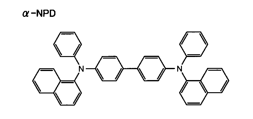
(発光層の形成)
次に、下記構造式に示すホスト材料H4の入った加熱ボートと、下記構造式に示す燐光発光性化合物Ir-4の入った加熱ボートとを、それぞれ独立に通電し、ホスト材料H4と燐光発光性化合物Ir-4とよりなる発光層55を、正孔輸送・注入層54上に形成した。この際、蒸着速度がホスト材料H4:燐光発光性化合物Ir-4=100:6となるように、加熱ボートの通電を調節した。また厚さ30nmとした。
次に、下記構造式に示すホスト材料H4の入った加熱ボートと、下記構造式に示す燐光発光性化合物Ir-4の入った加熱ボートとを、それぞれ独立に通電し、ホスト材料H4と燐光発光性化合物Ir-4とよりなる発光層55を、正孔輸送・注入層54上に形成した。この際、蒸着速度がホスト材料H4:燐光発光性化合物Ir-4=100:6となるように、加熱ボートの通電を調節した。また厚さ30nmとした。

(正孔阻止層の形成)
次に、正孔阻止材料として下記構造式に示すBAlqが入った加熱ボートに通電して加熱し、BAlqよりなる正孔阻止層56を、発光層55上に形成した。この際、蒸着速度0.1nm/秒~0.2nm/秒、厚さ10nmとした。
次に、正孔阻止材料として下記構造式に示すBAlqが入った加熱ボートに通電して加熱し、BAlqよりなる正孔阻止層56を、発光層55上に形成した。この際、蒸着速度0.1nm/秒~0.2nm/秒、厚さ10nmとした。

(電子輸送・注入層の形成)
その後、電子輸送材料として下記構造式に示す化合物10の入った加熱ボートと、フッ化カリウムの入った加熱ボートとを、それぞれ独立に通電し、化合物10とフッ化カリウムとよりなる電子注入層と電子輸送層とを兼ねた電子輸送・注入層57を、正孔阻止層56上に形成した。この際、蒸着速度が化合物10:フッ化カリウム=75:25になるように、加熱ボートの通電を調節した。また厚さ30nmとした。
その後、電子輸送材料として下記構造式に示す化合物10の入った加熱ボートと、フッ化カリウムの入った加熱ボートとを、それぞれ独立に通電し、化合物10とフッ化カリウムとよりなる電子注入層と電子輸送層とを兼ねた電子輸送・注入層57を、正孔阻止層56上に形成した。この際、蒸着速度が化合物10:フッ化カリウム=75:25になるように、加熱ボートの通電を調節した。また厚さ30nmとした。
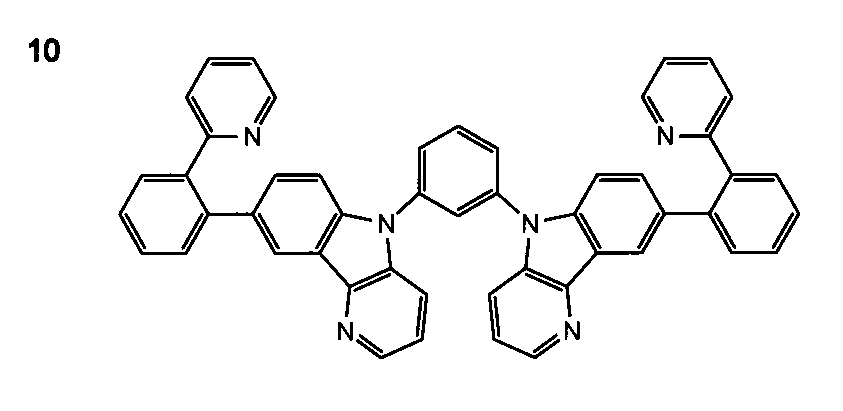
(対向電極:カソードの形成)
以上の後には、発光機能層が形成された透明基材52を、真空蒸着装置の第2真空槽内に移送し、第2真空槽内を4×10⁻⁴Paまで減圧した後、第2真空槽内に取り付けられたアルミニウムの入った抵抗加熱ボートを通電して加熱した。これにより、蒸着速度0.3nm/秒で厚さ100nmのアルミニウムからなる対向電極58を形成した。この対向電極58は、カソードとして用いられる。以上により透明基材52上に、ボトムエミッション型の有機EL素子を形成した。
以上の後には、発光機能層が形成された透明基材52を、真空蒸着装置の第2真空槽内に移送し、第2真空槽内を4×10⁻⁴Paまで減圧した後、第2真空槽内に取り付けられたアルミニウムの入った抵抗加熱ボートを通電して加熱した。これにより、蒸着速度0.3nm/秒で厚さ100nmのアルミニウムからなる対向電極58を形成した。この対向電極58は、カソードとして用いられる。以上により透明基材52上に、ボトムエミッション型の有機EL素子を形成した。
(素子の封止)
その後、有機EL素子を、厚さ300μmのガラス基板からなる封止材で覆い、有機EL素子を囲む状態で、透明封止材と透明基材52との間に接着剤(シール材)を充填した。接着剤としては、エポキシ系光硬化型接着剤(東亞合成社製ラックストラックLC0629B)を用いた。透明封止材と透明基材52との間に充填した接着剤に対して、ガラス基板(透明封止材)側からUV光を照射し、接着剤を硬化させて有機EL素子を封止した。
その後、有機EL素子を、厚さ300μmのガラス基板からなる封止材で覆い、有機EL素子を囲む状態で、透明封止材と透明基材52との間に接着剤(シール材)を充填した。接着剤としては、エポキシ系光硬化型接着剤(東亞合成社製ラックストラックLC0629B)を用いた。透明封止材と透明基材52との間に充填した接着剤に対して、ガラス基板(透明封止材)側からUV光を照射し、接着剤を硬化させて有機EL素子を封止した。
尚、有機EL素子の形成においては、各層の形成に蒸着マスクを使用し、5cm×5cmの透明基材52における中央の4.5cm×4.5cmを発光領域とし、発光領域の全周に幅0.25cmの非発光領域を設けた。また、アノードである透明電極51の導電層53と、カソードである対向電極58とは、正孔輸送・注入層54から電子輸送・注入層57によって絶縁された状態で、透明基材52の周縁に端子部分を引き出された形状で形成した。
以上のようにして、透明基材52上に有機EL素子を設け、これを透明封止材と接着剤とで封止した試料201~225の有機EL素子の各発光パネルを得た。これらの各発光パネルにおいては、発光層55で発生した各色の発光光hが、透明基材52側から取り出される。
[実施例2の各試料の評価]
試料201~225で作製した有機EL素子について、駆動電圧(V)、及び、色度差(Δxy)を測定した。この結果を下記表2に合わせて示す。
試料201~225で作製した有機EL素子について、駆動電圧(V)、及び、色度差(Δxy)を測定した。この結果を下記表2に合わせて示す。
[駆動電圧の測定方法]
駆動電圧の測定においては、各試料201~225の有機EL素子の透明電極51側(すなわち透明基材52側)での正面輝度が1000cd/m2となるときの電圧を駆動電圧として測定した。なお、輝度の測定には分光放射輝度計CS-1000(コニカミノルタセンシング製)を用いた。得られた駆動電圧の数値が小さいほど、好ましい結果であることを表わす。
駆動電圧の測定においては、各試料201~225の有機EL素子の透明電極51側(すなわち透明基材52側)での正面輝度が1000cd/m2となるときの電圧を駆動電圧として測定した。なお、輝度の測定には分光放射輝度計CS-1000(コニカミノルタセンシング製)を用いた。得られた駆動電圧の数値が小さいほど、好ましい結果であることを表わす。
[色変化の測定方法]
色変化の測定においては、各試料201~225の有機EL素子に2.5mA/cm2の電流を加え、角度の異なる位置からCIE1931表色系における色度を測定した。この際、透明電極51側の発光面に対する法線方向となる0°の位置と、垂直水平(上下左右)方向にそれぞれ45°の各位置とで色度を測定した。角度の異なる位置において測定した色度の差を、色変化(Δxy)として下記表2に示した。色変化は、色度の視野角特性を表し、数値が小さいほど好ましい結果となる。
色変化の測定においては、各試料201~225の有機EL素子に2.5mA/cm2の電流を加え、角度の異なる位置からCIE1931表色系における色度を測定した。この際、透明電極51側の発光面に対する法線方向となる0°の位置と、垂直水平(上下左右)方向にそれぞれ45°の各位置とで色度を測定した。角度の異なる位置において測定した色度の差を、色変化(Δxy)として下記表2に示した。色変化は、色度の視野角特性を表し、数値が小さいほど好ましい結果となる。
試料201~225の構成、並びに、駆動電圧(V)、及び、色度差(Δxy)の測定結果を下記表2に示す。

[実施例2の評価結果]
試料201~208では、作製した有機EL素子の発光が得られなかった。これは、プラズマ処理を行っていない透明電極の導電層の形成不良による。
試料201~208では、作製した有機EL素子の発光が得られなかった。これは、プラズマ処理を行っていない透明電極の導電層の形成不良による。
透明部材にプラズマ処理を行った後に導電層を形成した透明電極を用いた試料209~225は、駆動電圧、色変化において良好な結果が得られた。
高屈折率層を有する試料212~216は、試料209~211に比べると駆動電圧が低い結果が得られた。これは、透明電極の面抵抗に依存する結果である。
また、プラズマ処理から導電層の形成開始までの時間を、それぞれ変更した試料213、試料222~225では、プラズマ処理から導電層の形成開始までの時間が5分を超えると、駆動電圧、色変化共に悪化している。特に、7分以上での駆動電圧、色変化共に悪化が顕著になる。
この結果から、有機EL素子においても、透明電極において、プラズマ処理から導電層の形成開始までの時間を5分以内とすることが好ましい。
また、プラズマ処理から導電層の形成開始までの時間を、それぞれ変更した試料213、試料222~225では、プラズマ処理から導電層の形成開始までの時間が5分を超えると、駆動電圧、色変化共に悪化している。特に、7分以上での駆動電圧、色変化共に悪化が顕著になる。
この結果から、有機EL素子においても、透明電極において、プラズマ処理から導電層の形成開始までの時間を5分以内とすることが好ましい。
以上の結果から、透明部材の表面にプラズマ処理をした後、導電層を形成した透明電極を用いた有機EL素子は、低い駆動電圧での高輝度発光と安定した面発光が可能であることが確認された。
なお、本発明は上述の実施形態例において説明した構成に限定されるものではなく、その他本発明構成を逸脱しない範囲において種々の変形、変更が可能である。
10,30,51 透明電極、11,52 透明基材、12,53 導電層、13 高屈折率層、14 発光機能層、14a 正孔注入層、14b 正孔輸送層、14c,55 発光層、14d 電子輸送層、14e 電子注入層、15,58 対向電極、20,40,60 製造装置、21 保持部材、22 プラズマ処理部、23,26,32,42,46 真空チャンバ、24 プラズマ発生部、25 導電層形成部、27,33,43,47 供給部、28,48 導電性材料、31 高屈折率層形成部、34 高屈折率材料、41 発光機能層形成部、44 有機材料、45 対向電極形成部、50 有機EL素子、54 正孔輸送・注入層、56 正孔阻止層、57 電子輸送・注入層
Claims (9)
- 透明部材上に導電層を備える透明電極を製造する装置であって、
前記導電層が形成される前記透明部材の表面をプラズマ処理するプラズマ処理部と、
前記プラズマ処理に続いて、前記透明部材上に前記導電層を形成する導電層形成部と、を有し、
前記プラズマ処理部と前記導電層形成部とが、前記透明部材の表面を大気中に暴露することなく連続処理可能に備えられている
透明電極の製造装置。 - 前記導電層形成部が、銀(Ag)又は銀(Ag)を主成分とする合金の供給部を備える請求項1に記載の透明電極の製造装置。
- 前記導電層形成部は、少なくとも2つ以上の膜厚測定装置を備える請求項1に記載の透明電極の製造装置。
- 前記透明部材の搬送速度をv[m/s]とし、
前記プラズマ処理部のプラズマ処理終了位置から、前記導電層形成部の形成開始位置までの距離をd1[m]としたとき、
d1≦v×300
を満たす
請求項1に記載の透明電極の製造装置。 - 透明基材の保持部材を備え、
前記透明基材の表面をプラズマ処理した後、前記透明基材上に前記導電層が形成される請求項1に記載の透明電極の製造装置。 - 透明基材上に高屈折率層を形成する高屈折率層形成部を有し、
前記高屈折率層の表面をプラズマ処理した後、前記高屈折率層上に前記導電層が形成される請求項1に記載の透明電極の製造装置。 - 前記高屈折率層形成部が、二酸化チタン、酸化ニオブ、ITO、IZO、及び、ZnOから選ばれる少なくとも1種以上の供給部を備える請求項6に記載の透明電極の製造装置。
- 透明部材上に導電層が形成された透明電極を備える電子デバイスを製造する装置であって、
前記導電層が形成される前記透明部材の表面をプラズマ処理するプラズマ処理部と、
前記プラズマ処理に続いて、前記透明部材上に前記導電層を形成する導電層形成部と、を有し、
前記プラズマ処理部と前記導電層形成部とが、前記透明部材の表面を大気中に暴露することなく連続処理可能に備えられている
電子デバイスの製造装置。 - 前記透明電極上に発光機能層を形成する発光機能層形成部を備える請求項8に記載の電子デバイスの製造装置。
Priority Applications (1)
| Application Number | Priority Date | Filing Date | Title |
|---|---|---|---|
| JP2015518282A JPWO2014189094A1 (ja) | 2013-05-24 | 2014-05-21 | 透明電極の製造装置、及び、電子デバイスの製造装置 |
Applications Claiming Priority (2)
| Application Number | Priority Date | Filing Date | Title |
|---|---|---|---|
| JP2013-110090 | 2013-05-24 | ||
| JP2013110090 | 2013-05-24 |
Publications (1)
| Publication Number | Publication Date |
|---|---|
| WO2014189094A1 true WO2014189094A1 (ja) | 2014-11-27 |
Family
ID=51933645
Family Applications (1)
| Application Number | Title | Priority Date | Filing Date |
|---|---|---|---|
| PCT/JP2014/063522 Ceased WO2014189094A1 (ja) | 2013-05-24 | 2014-05-21 | 透明電極の製造装置、及び、電子デバイスの製造装置 |
Country Status (2)
| Country | Link |
|---|---|
| JP (1) | JPWO2014189094A1 (ja) |
| WO (1) | WO2014189094A1 (ja) |
Citations (6)
| Publication number | Priority date | Publication date | Assignee | Title |
|---|---|---|---|---|
| JPH09176837A (ja) * | 1995-12-21 | 1997-07-08 | Toppan Printing Co Ltd | 透明導電膜 |
| JP2002015623A (ja) * | 2000-04-27 | 2002-01-18 | Mitsui Chemicals Inc | 透明電極 |
| JP2004006171A (ja) * | 2002-06-03 | 2004-01-08 | Mitsui Chemicals Inc | 透明導電性フィルムの製造方法 |
| JP2008184625A (ja) * | 2007-01-26 | 2008-08-14 | Osaka Vacuum Ltd | スパッタ方法及びスパッタ装置 |
| JP2011248629A (ja) * | 2010-05-27 | 2011-12-08 | Meihan Shinku Kogyo Kk | 透明導電性基材 |
| JP2012237057A (ja) * | 2011-04-28 | 2012-12-06 | Nitto Denko Corp | 真空成膜方法、及び該方法によって得られる積層体 |
-
2014
- 2014-05-21 JP JP2015518282A patent/JPWO2014189094A1/ja active Pending
- 2014-05-21 WO PCT/JP2014/063522 patent/WO2014189094A1/ja not_active Ceased
Patent Citations (6)
| Publication number | Priority date | Publication date | Assignee | Title |
|---|---|---|---|---|
| JPH09176837A (ja) * | 1995-12-21 | 1997-07-08 | Toppan Printing Co Ltd | 透明導電膜 |
| JP2002015623A (ja) * | 2000-04-27 | 2002-01-18 | Mitsui Chemicals Inc | 透明電極 |
| JP2004006171A (ja) * | 2002-06-03 | 2004-01-08 | Mitsui Chemicals Inc | 透明導電性フィルムの製造方法 |
| JP2008184625A (ja) * | 2007-01-26 | 2008-08-14 | Osaka Vacuum Ltd | スパッタ方法及びスパッタ装置 |
| JP2011248629A (ja) * | 2010-05-27 | 2011-12-08 | Meihan Shinku Kogyo Kk | 透明導電性基材 |
| JP2012237057A (ja) * | 2011-04-28 | 2012-12-06 | Nitto Denko Corp | 真空成膜方法、及び該方法によって得られる積層体 |
Also Published As
| Publication number | Publication date |
|---|---|
| JPWO2014189094A1 (ja) | 2017-02-23 |
Similar Documents
| Publication | Publication Date | Title |
|---|---|---|
| JP6337883B2 (ja) | 電子デバイス | |
| WO2011132550A1 (ja) | 有機エレクトロルミネッセンス素子、表示装置及び照明装置 | |
| JP6592915B2 (ja) | 透明電極基板とその製造方法、電子デバイス及び有機elデバイス | |
| JPWO2012172883A1 (ja) | 有機エレクトロルミネッセンス素子の製造方法 | |
| WO2010084815A1 (ja) | 有機エレクトロルミネッセンス素子及びその製造方法 | |
| JPWO2009116414A1 (ja) | 有機エレクトロルミネッセンス素子 | |
| JP5673335B2 (ja) | 有機エレクトロルミネッセンス素子 | |
| JP2010073590A (ja) | 有機エレクトロルミネッセンス素子の製造方法及び有機エレクトロルミネッセンス素子 | |
| JP2016012417A (ja) | 有機エレクトロルミネッセンス素子、及び、電子デバイス | |
| JP2010177338A (ja) | 有機エレクトロルミネッセンス素子及びその製造方法 | |
| JP5655486B2 (ja) | 有機エレクトロルミネッセンス素子の製造方法 | |
| JP2009289716A (ja) | 有機エレクトロルミネセンス素子及びその製造方法 | |
| WO2007077715A1 (ja) | ボトムエミッション型有機エレクトロルミネッセンスパネル | |
| JP6687013B2 (ja) | 透明電極及び電子デバイス | |
| WO2014109265A1 (ja) | 透明電極、及び、電子デバイス | |
| JP2015156253A (ja) | 有機エレクトロルミネッセンス素子およびその製造方法 | |
| WO2010084816A1 (ja) | 有機エレクトロルミネッセンス素子及びその製造方法 | |
| WO2018116923A1 (ja) | 透明電極及び電子デバイス | |
| WO2014189094A1 (ja) | 透明電極の製造装置、及び、電子デバイスの製造装置 | |
| WO2018083974A1 (ja) | 有機エレクトロルミネッセンス素子、及び、発光装置 | |
| JP2012234972A (ja) | 有機エレクトロルミネッセンス素子及び有機エレクトロルミネッセンス素子の製造方法 | |
| JP5266533B2 (ja) | 有機エレクトロルミネッセンス素子の製造方法および照明装置 | |
| JPWO2015118919A1 (ja) | 有機エレクトロルミネッセンス照明装置 | |
| WO2014181695A1 (ja) | 有機エレクトロルミネッセンス素子 | |
| JP2012169199A (ja) | 有機エレクトロルミネッセンス素子 |
Legal Events
| Date | Code | Title | Description |
|---|---|---|---|
| 121 | Ep: the epo has been informed by wipo that ep was designated in this application |
Ref document number: 14801842 Country of ref document: EP Kind code of ref document: A1 |
|
| ENP | Entry into the national phase |
Ref document number: 2015518282 Country of ref document: JP Kind code of ref document: A |
|
| NENP | Non-entry into the national phase |
Ref country code: DE |
|
| 122 | Ep: pct application non-entry in european phase |
Ref document number: 14801842 Country of ref document: EP Kind code of ref document: A1 |