WO2014188802A1 - Esd保護装置 - Google Patents
Esd保護装置 Download PDFInfo
- Publication number
- WO2014188802A1 WO2014188802A1 PCT/JP2014/059994 JP2014059994W WO2014188802A1 WO 2014188802 A1 WO2014188802 A1 WO 2014188802A1 JP 2014059994 W JP2014059994 W JP 2014059994W WO 2014188802 A1 WO2014188802 A1 WO 2014188802A1
- Authority
- WO
- WIPO (PCT)
- Prior art keywords
- discharge
- electrode
- esd protection
- discharge electrode
- conductor
- Prior art date
- Legal status (The legal status is an assumption and is not a legal conclusion. Google has not performed a legal analysis and makes no representation as to the accuracy of the status listed.)
- Ceased
Links
Images




Classifications
-
- H—ELECTRICITY
- H01—ELECTRIC ELEMENTS
- H01T—SPARK GAPS; OVERVOLTAGE ARRESTERS USING SPARK GAPS; SPARKING PLUGS; CORONA DEVICES; GENERATING IONS TO BE INTRODUCED INTO NON-ENCLOSED GASES
- H01T4/00—Overvoltage arresters using spark gaps
- H01T4/10—Overvoltage arresters using spark gaps having a single gap or a plurality of gaps in parallel
- H01T4/12—Overvoltage arresters using spark gaps having a single gap or a plurality of gaps in parallel hermetically sealed
Definitions
- the present invention relates to an ESD protection device.
- Patent Document 1 a ceramic multilayer substrate and a pair disposed in the ceramic multilayer substrate and disposed so that the tips thereof face each other with a gap in a cavity provided in the ceramic multilayer substrate.
- An ESD protection device comprising a plurality of discharge electrodes is described.
- the first and second discharge electrodes are provided in the ceramic multilayer substrate, and are further connected to the first and second discharge electrodes.
- An auxiliary electrode is provided.
- the auxiliary electrode is formed by dispersing a conductive material coated with an inorganic material having no conductivity.
- the ESD protection device described in Patent Document 1 has a problem that it does not operate when the discharge start voltage is low. On the other hand, in the ESD protection device described in Patent Document 2, the discharge start voltage is lowered by the auxiliary electrode, but this is not sufficient.
- the main object of the present invention is to provide an ESD protection device that can lower the discharge start voltage.
- the ESD protection device includes an insulating material, first and second discharge electrodes, a first external electrode, a second external electrode, and a conductor.
- the first and second discharge electrodes are provided in the insulating material.
- the first external electrode is provided on the outer surface of the insulating material.
- the first external electrode is electrically connected to the first discharge electrode.
- the second external electrode is provided on the outer surface of the insulating material.
- the second external electrode is electrically connected to the second discharge electrode.
- the conductor is provided in the insulating material. The conductor is not connected to the first and second external electrodes.
- the first discharge electrode and the second discharge electrode are provided so as to face each other.
- the conductor is provided so as to overlap with the facing portions of the first and second discharge electrodes in plan view.
- the conductor is both an upper part of the opposing part of the first and second discharge electrodes and a lower part of the opposing part of the first and second discharge electrodes. Is provided.
- the insulating material has a cavity.
- Each of the front end portion of the first discharge electrode and the front end portion of the second discharge electrode is located in the cavity.
- the conductor is provided so as to overlap the cavity in plan view.
- the ESD protection apparatus further includes a discharge auxiliary electrode.
- the discharge auxiliary electrode is disposed between the tip portion of the first discharge electrode and the tip portion of the second discharge electrode.
- the discharge auxiliary electrode promotes discharge between the first discharge electrode and the second discharge electrode.
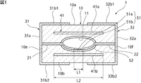
- FIG. 1 is a schematic cross-sectional view of an ESD protection apparatus according to an embodiment of the present invention.
- FIG. 2 is a schematic plan view of an ESD protection apparatus according to an embodiment of the present invention.
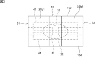
- FIG. 3 is a schematic plan view of the ESD protection apparatus according to the first modification.
- FIG. 4 is a schematic plan view of the ESD protection apparatus according to the second modification.
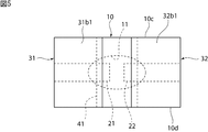
- FIG. 5 is a schematic plan view of an ESD protection apparatus according to a third modification.
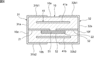
- FIG. 6 is a schematic cross-sectional view of an ESD protection apparatus according to a fourth modification.
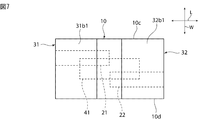
- FIG. 7 is a schematic plan view of an ESD protection apparatus according to a fifth modification.
- FIG. 8 is a schematic plan view of an ESD protection apparatus according to a sixth modification.
- FIG. 9 is a schematic plan view of an ESD protection apparatus according to a seventh modification.
- FIG. 10 is a schematic plan view of an ESD protection apparatus according to an eighth modification.
- FIG. 1 is a schematic cross-sectional view of an ESD protection apparatus according to an embodiment of the present invention.
- FIG. 2 is a schematic plan view of an ESD protection apparatus according to an embodiment of the present invention.
- the ESD protection device 1 has an insulating material 10 having a cavity 11.
- the insulating material 10 is a hexahedron.
- hexahedron means a general solid having six faces. Each of the six surfaces constituting the hexahedron may be non-planar. Of the surfaces constituting the hexahedron, the opposing surfaces may be parallel to each other or non-parallel. The corners and ridges of the hexahedron may each be chamfered or have a rounded shape.
- the insulating material 10 is provided in a substantially rectangular parallelepiped shape.
- the insulating material 10 includes first and second main faces 10a and 10b that are parallel to each other, first and second side faces 10c and 10d that are parallel to each other, and first and second end faces 10e and 10f that are parallel to each other.
- the insulating material 10 can be composed of appropriate ceramics. Specifically, the insulating material 10 can be made of, for example, low temperature co-fired ceramics (LTCC: Low Temperature Co-fired Ceramics) containing Ba, Al, and Si as main components. Note that a resin substrate containing polyimide resin, epoxy resin, or the like may be used as the insulating material 10.
- LTCC Low Temperature Co-fired Ceramics
- the first and second discharge electrodes 21 and 22 are provided inside the insulating material 10.
- the first and second discharge electrodes 21 and 22 are provided in parallel with the first and second main surfaces 10a and 10b, respectively.
- the first discharge electrode 21 is drawn out to the first end face 10e.
- the second discharge electrode 22 is drawn out to the second end face 10f.
- the distal end portion of the first discharge electrode 21 and the distal end portion of the second discharge electrode 22 are located in the cavity 11.
- the front end portion of the first discharge electrode 21 and the front end portion of the second discharge electrode 22 are opposed to each other in the cavity 11.
- First and second external electrodes 31 and 32 are provided on the outer surface of the insulating material 10. Specifically, the first external electrode 31 is provided on at least one of the first portion 31a provided on the first end face 10e and the first and second main faces 10a and 10b. And second portions 31b1 and 31b2. However, the first external electrode may be provided only on the first end face. The first external electrode 31 is electrically connected to the first discharge electrode 21 in the first portion 31a.
- the second external electrode 32 includes a third portion 32a provided on the second end surface 10f and a fourth portion provided on at least one of the first and second main surfaces 10a and 10b. 32b1 and 32b2. However, the second external electrode may be provided only on the second end face. The second external electrode 32 is electrically connected to the second discharge electrode 22 in the third portion 32a.
- a discharge auxiliary electrode 51 is disposed between the tip portion of the first discharge electrode 21 and the tip portion of the second discharge electrode 22.
- the discharge auxiliary electrode is provided between the first and second discharge electrodes and the insulating material 10 in addition to between the tip portion of the first discharge electrode and the tip portion of the second discharge electrode. It may be.
- the discharge auxiliary electrode 51 has a function of reducing the discharge start voltage. Specifically, by providing the discharge auxiliary electrode 51, creeping discharge via the discharge auxiliary electrode 51 occurs. Usually, the creeping discharge, the air discharge, and the discharge through the discharge auxiliary electrode 51 have the lowest starting voltage of the discharge through the discharge auxiliary electrode 51. Therefore, by providing the discharge auxiliary electrode 51, the discharge start voltage can be lowered.
- the discharge auxiliary electrode 51 can be constituted by, for example, a particle dispersion in which a plurality of metal particles 51a whose surfaces are coated with an inorganic material having no conductivity and a plurality of semiconductor ceramic particles 51b are dispersed.
- the discharge auxiliary electrode 51 is formed, for example, by applying and baking a paste containing a plurality of metal particles 51a whose surfaces are coated with an inorganic material having no conductivity and a plurality of semiconductor ceramic particles 51b. be able to.
- the metal particles 51a can be made of, for example, Cu or Ni.
- the diameter of the metal particles 51a can be, for example, about 2 ⁇ m to 3 ⁇ m.
- the coating film of the metal particles 51a can be made of, for example, aluminum oxide.
- the semiconductor ceramic particles 51b include, for example, carbides such as silicon carbide, titanium carbide, zirconium carbide, molybdenum carbide or tungsten carbide, nitrides such as titanium nitride, zirconium nitride, chromium nitride, vanadium nitride or tantalum nitride, titanium silicide, silica Silicides such as zirconium silicide, tungsten silicide, molybdenum silicide, chromium silicide, boride such as titanium boride, zirconium boride, chromium boride, lanthanum boride, molybdenum boride, tungsten boride, zinc oxide, An oxide such as strontium titanate can be used.
- carbides such as silicon carbide, titanium carbide, zirconium carbide, molybdenum carbide or tungsten carbide
- nitrides such as titanium nit
- the discharge auxiliary electrode 51 may further include insulating particles made of aluminum oxide or the like in addition to the metal particles 51a and the semiconductor ceramic particles 51b.
- a protective layer 52 is provided between the insulating material 10 and at least one tip of the first and second discharge electrodes 21 and 22. Specifically, the protective layer 52 is provided so as to cover substantially the entire inner wall of the cavity 11. However, the protective layer 52 is not necessarily provided. When the protective layer 52 is not provided, there is an advantage that the distance between the discharge electrode facing portion and the conductor can be shortened.
- the protective layer 52 is preferably made of a ceramic having a sintering temperature higher than that of the ceramic constituting the insulating material 10.
- the protective layer 52 preferably contains at least one selected from the group consisting of alumina, mullite, zirconia, magnesia and quartz, for example.
- a conductor 41 is provided in the insulating material 10. But the conductor 41 does not necessarily need to be provided in the inside of the insulating material 10, and may be provided on the surface of the insulating material 10. Further, a plurality of conductors 41 may be provided at intervals from each other along the thickness direction of the insulating material 10.
- the conductor 41 is provided so as not to be connected to the first and second external electrodes 31 and 32.
- the conductor 41 is preferably provided so as to overlap with the facing portions of the discharge electrodes 21 and 22 when viewed in plan. Further, the closer the distance between the conductor 41 and the discharge electrode facing portion in the thickness direction, the greater the effect of promoting electric field concentration at the tips of the discharge electrodes 21 and 22.
- auxiliary discharge electrode 51 when the auxiliary discharge electrode 51 is provided between the discharge electrodes 21 and 22, creeping discharge on the auxiliary discharge electrode 51 becomes active. This effect is greater as the conductor 41 is closer to the auxiliary discharge electrode 51 side in the thickness direction.
- the conductor 41 As the conductor 41, the conductor 41 a is provided above the opposing portion of the first and second discharge electrodes 21, 22, and is provided below the opposing portion of the first and second discharge electrodes 21, 22. A conductor 41b is provided. But the conductor 41 does not necessarily need to be provided in both the upper part and the lower part of the opposing part of the 1st and 2nd discharge electrodes 21 and 22, and should just be provided in at least one.
- the conductor 41 is rectangular when viewed in plan.
- the length L2 of the conductor 41 shown in FIG. 1 is preferably longer than the distance L1 between the distal end portion of the first discharge electrode 21 and the distal end portion of the second discharge electrode 22.
- the conductor 41, the first and second discharge electrodes 21, 22 and the first and second external electrodes 31, 32 are each at least one of Cu, Ag, Pd, Pt, Al, Ni, and W, for example. It can be made of a metal (including an alloy) containing The conductor 41, the first and second discharge electrodes 21, 22 and the first and second outer electrodes 31, 32 are preferably made of the same material.
- the discharge start voltage can be further reduced. This is because electric field concentration is promoted on the surfaces of the first and second discharge electrodes 21 and 22, particularly at the tips, by arranging the conductor 41 in the vicinity of the first and second discharge electrodes 21 and 22. It is. Therefore, the movement of electrons as a starting point of discharge is promoted by the electric field concentration. As a result, the discharge start voltage is considered to be low.
- the shape of the conductor 41 is not limited to the shape shown in FIG.1 and FIG.2.
- conductors 41 arranged in the width direction may be provided.
- a conductor 41 may be provided so as to cover not only the first and second external electrodes 31 and 32 and the opposing portions thereof but also the cavity 11.
- a conductor 41 may be provided so as to connect the side surface 10c and the side surface 10d.
- the insulating material 10 may not have a cavity.
- the discharge auxiliary electrode 51 is not necessarily provided.
- a porous layer in which a material having a voltage nonlinearity characteristic, a metal, a semiconductor, or the like is dispersed may be provided.
- the distal end portion of the first discharge electrode 21 and the distal end portion of the second discharge electrode 22 face each other in the direction in which the discharge electrodes 21 and 22 extend (length direction L) will be described.
- the present invention is not limited to this configuration.
- the distal end portion of the first discharge electrode 21 and the distal end portion of the second discharge electrode 22 extend in the direction in which the discharge electrodes 21 and 22 extend (length direction L). May not face each other.
- the position in the width direction W of the tip portion of the first discharge electrode 21 is different from the position in the width direction W of the tip portion of the second discharge electrode 22.
- the position in the length direction L of the tip portion of the first discharge electrode 21 and the position in the length direction L of the tip portion of the second discharge electrode 22 are substantially the same. For this reason, the corner on one side in the width direction W of the first discharge electrode 21 and the corner on the other side in the width direction W of the second discharge electrode 22 face each other.
- the position of the tip portion of the first discharge electrode 21 in the width direction W is different from the position of the tip portion of the second discharge electrode 22 in the width direction W.
- a part of the first discharge electrode 21 and a part of the second discharge electrode 22 face each other in the width direction W.
- a part of the first discharge electrode 21 and a part of the second discharge electrode 22 face each other in the width direction W.
- the shortest distance between the portions where the first discharge electrode 21 and the second discharge electrode 22 face each other in the width direction W is between the tip of the first discharge electrode 21 and the second discharge electrode 22.
- the distance in the length direction L is shorter than each of the distance in the length direction L between the tip portion of the second discharge electrode 22 and the first discharge electrode 21. For this reason, a discharge occurs in a portion where the first discharge electrode 21 and the second discharge electrode 22 face each other in the width direction W.
- Ceramics used for the construction of the insulating material BAS material mainly composed of Ba, Al and Si Discharge electrode, external electrode, conductor: Cu Dimensions of ESD protection device: length 1.0mm x width 0.5mm x thickness 0.3mm Planar shape of the cavity: rectangular shape Discharge gap L1: 20 ⁇ m Discharge auxiliary electrode L1: 20 ⁇ m Cavity length: 200 ⁇ m Conductor: Located below the auxiliary electrode through the insulating part. Distance L2: 20 ⁇ m
- the ESD protection devices shown in the example in which the conductor was provided and the comparative example in which the conductor was not provided were manufactured, and the operation rate at each load voltage was evaluated by a contact discharge test in accordance with IEC61000-4-2. In 100 samples, the number of samples in which discharge started is obtained, and the ratio is used as the operation rate.
- the operating rate evaluation symbols are as follows.
Landscapes
- Thermistors And Varistors (AREA)
Abstract
放電開始電圧をより低めることができるESD保護装置を提供する。 ESD保護装置(1)は、絶縁材(10)と、第1及び第2の放電電極(21,22)と、第1の外部電極(31)と、第2の外部電極(32)と、導体(41)とを備える。第1及び第2の放電電極(21,22)は、絶縁材(10)中に設けられている。第1の外部電極(31)は、絶縁材(10)の外表面上に設けられている。第1の外部電極(31)は、第1の放電電極(21)に電気的に接続されている。第2の外部電極(32)は、絶縁材(10)の外表面上に設けられている。第2の外部電極(32)は、第2の放電電極(22)に電気的に接続されている。導体(41)は、絶縁材(10)中に設けられている。導体(41)は、第1及び第2の外部電極(31,32)と接続していない。
Description
本発明は、ESD保護装置に関する。
従来、静電気放電(ESD:electro-static discharge)による電子機器の破壊を抑制するためのESD保護装置が種々提案されている。
例えば、下記の特許文献1には、セラミック多層基板と、セラミック多層基板内に配されており、セラミック多層基板に設けられた空洞部において間隔をおいて先端同士が対向するように配された一対の放電電極とを備えるESD保護装置が記載されている。
また、下記の特許文献2に記載のESD保護装置では、セラミック多層基板内に第1,第2の放電電極が設けられており、さらに、第1,第2の放電電極に接続されるように、補助電極が設けられている。補助電極は、導電性を有しない無機材料によりコーティングされた導電性材料を分散させることにより形成されている。
特許文献1に記載のESD保護装置は、放電開始電圧が低い場合、動作しないという問題点があった。他方、特許文献2に記載のESD保護装置では、補助電極により放電開始電圧の低電圧化が図られているが、なお十分ではなかった。
本発明は、放電開始電圧をより低くすることができる、ESD保護装置を提供することを主な目的とする。
本発明に係るESD保護装置は、絶縁材と、第1及び第2の放電電極と、第1の外部電極と、第2の外部電極と、導体とを備える。第1及び第2の放電電極は、絶縁材中に設けられている。第1の外部電極は、絶縁材の外表面上に設けられている。第1の外部電極は、第1の放電電極に電気的に接続されている。第2の外部電極は、絶縁材の外表面上に設けられている。第2の外部電極は、第2の放電電極に電気的に接続されている。導体は、絶縁材中に設けられている。導体は、第1及び第2の外部電極に接続していない。
本発明に係るESD保護装置のある特定の局面では、第1の放電電極と第2の放電電極とは、互いに対向するように設けられている。導体は、平面視において第1及び第2の放電電極の対向部と重なるように設けられている。
本発明に係るESD保護装置の他の特定局面では、導体が、第1及び第2の放電電極の対向部の上方部と、第1及び第2の放電電極の対向部の下方部との両方に設けられている。
本発明に係るESD保護装置の別の特定の局面では、絶縁材は、空洞を有する。第1の放電電極の先端部と第2の放電電極の先端部とのそれぞれが空洞内に位置している。
本発明に係るESD保護装置の他の特定の局面では、導体は、平面視において空洞と重なるように設けられている。
本発明に係るESD保護装置のさらにまた他の特定の局面では、ESD保護装置は、放電補助電極をさらに備える。放電補助電極は、第1の放電電極の先端部と第2の放電電極の先端部との間に配されている。放電補助電極は、第1の放電電極と第2の放電電極との間の放電を促す。
本発明によれば、放電開始電圧をより低くすることができる、ESD保護装置を提供することができる。
以下、本発明を実施した好ましい形態の一例について説明する。但し、下記の実施形態は、単なる例示である。本発明は、下記の実施形態に何ら限定されない。
また、実施形態等において参照する各図面において、実質的に同一の機能を有する部材は同一の符号で参照することとする。また、実施形態等において参照する図面は、模式的に記載されたものであり、図面に描画された物体の寸法の比率などは、現実の物体の寸法の比率などとは異なる場合がある。図面相互間においても、物体の寸法比率等が異なる場合がある。具体的な物体の寸法比率等は、以下の説明を参酌して判断されるべきである。
図1は、本発明の一実施形態に係るESD保護装置の略図的断面図である。図2は、本発明の一実施形態に係るESD保護装置の略図的平面図である。
図1及び図2に示されるように、ESD保護装置1は、空洞11を有する絶縁材10を有する。絶縁材10は、六面体である。ここで、「六面体」とは、6つの面を有する立体全般を意味する。六面体を構成する6つの面は、それぞれ、非平面であってもよい。六面体を構成する面のうち、対向する面は、互いに平行であってもよいし、非平行であってもよい。六面体の角部及び稜線部は、それぞれ、面取り状であってもよいし、丸められた形状を有していてもよい。本実施形態では、具体的には、絶縁材10は、略直方体状に設けられている。絶縁材10は、互いに平行な第1及び第2の主面10a、10bと、互いに平行な第1及び第2の側面10c、10dと、互いに平行な第1及び第2の端面10e、10fとを有する。
絶縁材10は、適宜のセラミックスにより構成することができる。具体的には、絶縁材10は、例えば、Ba、Al、Siを主成分として含む低温同時焼成セラミックス(LTCC:Low Temperature Co-fired Ceramics)により構成することができる。なお、絶縁材10として、ポリイミド樹脂、エポキシ樹脂などを含む樹脂基板を用いてもよい。
絶縁材10の内部には、第1及び第2の放電電極21,22が設けられている。第1及び第2の放電電極21,22は、それぞれ、第1及び第2の主面10a、10bと平行に設けられている。第1の放電電極21は、第1の端面10eに引き出されている。一方、第2の放電電極22は、第2の端面10fに引き出されている。第1の放電電極21の先端部と、第2の放電電極22の先端部とは、空洞11内に位置している。第1の放電電極21の先端部と、第2の放電電極22の先端部とは、空洞11内において対向している。
このような構成にすることにより、空洞内ガスと放電電極と基板のトリプルジャンクションを形成する。結果、ESD保護装置1の応答性が向上する。
絶縁材10の外表面の上には、第1及び第2の外部電極31,32が設けられている。具体的には、第1の外部電極31は、第1の端面10eの上に設けられた第1の部分31aと、第1及び第2の主面10a、10bの少なくとも一方の上に設けられた第2の部分31b1,31b2とを有する。もっとも、第1の外部電極は、第1の端面の上のみに設けられていてもよい。第1の外部電極31は、第1の部分31aにおいて第1の放電電極21と電気的に接続されている。
第2の外部電極32は、第2の端面10fの上に設けられた第3の部分32aと、第1及び第2の主面10a、10bの少なくとも一方の上に設けられた第4の部分32b1,32b2とを有する。もっとも、第2の外部電極は、第2の端面の上にのみ設けられていてもよい。第2の外部電極32は、第3の部分32aにおいて第2の放電電極22と電気的に接続されている。
空洞11の内面上において、第1の放電電極21の先端部と第2の放電電極22の先端部との間には、放電補助電極51が配されている。もっとも、放電補助電極は、第1の放電電極の先端部と第2の放電電極の先端部との間に加えて、第1及び第2の放電電極と絶縁材10との間にも設けられていてもよい。
放電補助電極51は、放電開始電圧を低下させる機能を有する。具体的には、放電補助電極51を設けることにより、放電補助電極51を経由した沿面放電が生じる。通常、沿面放電と気中放電と放電補助電極51を経由した放電とでは、放電補助電極51を経由した放電の開始電圧が最も低い。従って、放電補助電極51を設けることにより、放電開始電圧を低下させることができる。
放電補助電極51は、例えば、導電性を有しない無機材料により表面がコーティングされた複数の金属粒子51aと、複数の半導体セラミック粒子51bとが分散した粒子分散体によって構成することができる。この場合、放電補助電極51は、例えば、導電性を有しない無機材料により表面がコーティングされた複数の金属粒子51aと、複数の半導体セラミック粒子51bを含むペーストを塗布し、焼成することにより形成することができる。
金属粒子51aは、例えば、CuやNiなどにより構成することができる。金属粒子51aの直径は、例えば2μm~3μm程度とすることができる。金属粒子51aのコーティング膜は、例えば、酸化アルミニウム等により構成することができる。
半導体セラミック粒子51bは、例えば、炭化ケイ素、炭化チタン、炭化ジルコニウム、炭化モリブデンもしくは炭化タングステン等の炭化物、窒化チタン、窒化ジルコニウム、窒化クロム、窒化バナジウムもしくは窒化タンタル等の窒化物、ケイ化チタン、ケイ化ジルコニウム、ケイ化タングステン、ケイ化モリブデン、ケイ化クロム等のケイ化物、ホウ化チタン、ホウ化ジルコニウム、ホウ化クロム、ホウ化ランタン、ホウ化モリブデン、ホウ化タングステンなどのホウ化物、酸化亜鉛、チタン酸ストロンチウム等の酸化物などにより構成することができる。
放電補助電極51は、金属粒子51a及び半導体セラミック粒子51bに加え、酸化アルミニウムなどからなる絶縁性粒子をさらに含んでいてもよい。
絶縁材10と第1及び第2の放電電極21,22の少なくとも一方の先端部との間には、保護層52が設けられている。具体的には、保護層52は、空洞11の内壁の実質的に全体を覆うように設けられている。ただし、保護層52は必ずしも設けられていなくてもよい。保護層52が設けられていない場合には、放電電極対向部と導体との距離を短くすることができるという利点がある。
保護層52は、絶縁材10を構成しているセラミックスよりも焼結温度が高いセラミックスにより構成されていることが好ましい。保護層52は、例えば、アルミナ、ムライト、ジルコニア、マグネシア及び石英からなる群から選ばれた少なくとも一種を含んでいることが好ましい。
絶縁材10中には、導体41が設けられている。もっとも、導体41は必ずしも絶縁材10の内部に設けられている必要はなく、絶縁材10の表面上に設けられていてもよい。また、導体41は、絶縁材10の厚み方向に沿って相互に間隔をおいて複数設けられていてもよい。
導体41は、第1及び第2の外部電極31,32と接続しないように設けられている。導体41は、平面視した場合、放電電極21,22の対向部と重なるように設けられていることが好ましい。また、厚み方向における導体41と放電電極対向部との距離が近いほど、放電電極21,22の先端において電界集中が促進される効果が大きい。
また、放電電極21,22間に放電補助電極51を有する場合は放電補助電極51上での沿面放電が活発になる。この効果は、厚み方向において導体41が放電補助電極51側に近いほど大きい。
本実施形態においては、導体41として、第1及び第2の放電電極21,22の対向部の上方部に導体41aが、第1及び第2の放電電極21,22の対向部の下方部に導体41bが設けられている。もっとも、導体41は、必ずしも、第1及び第2の放電電極21,22の対向部の上方と下方の両方に設けられている必要はなく、少なくとも一方に設けられていればよい。導体41は平面視した場合、矩形である。図1に示す導体41の長さL2は、第1の放電電極21の先端部と第2の放電電極22の先端部との間の距離L1よりも長いことが好ましい。
なお、導体41、第1及び第2の放電電極21,22並びに第1及び第2の外部電極31,32は、それぞれ、例えば、Cu,Ag、Pd,Pt,Al,Ni及びWの少なくとも一種を含む金属(合金を含む)などにより構成することができる。導体41、第1及び第2の放電電極21,22並びに第1及び第2の外部電極31,32は、同じ材料により構成されていることが好ましい。
導体41を配置することにより、放電開始電圧をより低めることができる。これは、第1及び第2の放電電極21,22の近傍に導体41が配置されることによって、第1及び第2の放電電極21,22の表面、特に先端において電界集中が促進されるためである。従って、電界集中により、放電の基点となる電子の移動が促される。その結果、放電開始電圧が低くなるものと考えられる。
なお、導体41の形状は、図1及び図2に示す形状に限定されない。
例えば、図3に示されるように、幅方向に沿って配列された導体41を設けてもよい。
図4に示されるように、第1及び第2の外部電極31,32並びにその対向部分だけでなく、空洞11を覆うように導体41を設けてもよい。
図5に示されるように、側面10cと側面10dを接続するように導体41を設けてもよい。
なお、図6に示されるように、絶縁材10に空洞が設けられていなくてもよい。また、放電補助電極51は、必ずしも設けられていなくてもよい。例えば、放電補助電極51の代わりに、電圧非直線性特性を有する材料、金属または半導体等が分散されたポーラスな層が設けられていてもよい。
上記実施形態では、第1の放電電極21の先端部と、第2の放電電極22の先端部とが、放電電極21,22の延びる方向(長さ方向L)において対向している例について説明した。但し、本発明は、この構成に限定されない。例えば、図7~図10に示されるように、第1の放電電極21の先端部と、第2の放電電極22の先端部とが、放電電極21,22の延びる方向(長さ方向L)において対向していなくてもよい。
図7に示される例では、第1の放電電極21の先端部の幅方向Wにおける位置と、第2の放電電極22の先端部の幅方向Wにおける位置とが異なっている。第1の放電電極21の先端部の長さ方向Lにおける位置と、第2の放電電極22の先端部の長さ方向Lにおける位置とが略同じである。このため、第1の放電電極21の幅方向Wにおける一方側の角部と、第2の放電電極22の幅方向Wにおける他方側の角部とが互いに対向している。
図8及び図9に示される例においても、第1の放電電極21の先端部の幅方向Wにおける位置と、第2の放電電極22の先端部の幅方向Wにおける位置とが異なっている。第1の放電電極21の一部と、第2の放電電極22の一部とは、幅方向Wにおいて対向している。
同様に、図10に示される例においても、第1の放電電極21の一部と、第2の放電電極22の一部とは、幅方向Wにおいて対向している。第1の放電電極21と第2の放電電極22とが幅方向Wに互いに対向している部分の最短距離は、第1の放電電極21の先端部と第2の放電電極22との間の長さ方向Lにおける距離と、第2の放電電極22の先端部と第1の放電電極21との間の長さ方向Lにおける距離とのそれぞれよりも短い。このため、第1の放電電極21と第2の放電電極22とが幅方向Wに互いに対向している部分において放電が生じる。
(実施例)
下記の条件で、上記実施形態に係るESD保護装置1と実質的に同様の構成を有するESD保護装置を作製した。
下記の条件で、上記実施形態に係るESD保護装置1と実質的に同様の構成を有するESD保護装置を作製した。
絶縁材の構成に用いたセラミックス:Ba、Al及びSiを主体とするBAS材
放電電極、外部電極、導体:Cu
ESD保護装置の寸法:長さ1.0mm×幅0.5mm×厚み0.3mm
空洞の平面視形状:矩形状
放電ギャップL1:20μm
放電補助電極L1:20μm
空洞の長さ:200μm
導体:絶縁部を介し、補助電極の下側に位置する。
距離L2:20μm
放電電極、外部電極、導体:Cu
ESD保護装置の寸法:長さ1.0mm×幅0.5mm×厚み0.3mm
空洞の平面視形状:矩形状
放電ギャップL1:20μm
放電補助電極L1:20μm
空洞の長さ:200μm
導体:絶縁部を介し、補助電極の下側に位置する。
距離L2:20μm
(比較例)
導体を設けなかったこと以外は、実施例と同様にしてESD保護装置を作製した。
導体を設けなかったこと以外は、実施例と同様にしてESD保護装置を作製した。
(放電開始電圧評価)
導体を設けた実施例と、導体を設けない比較例に示すESD保護装置を作製し、IEC61000-4-2に準拠した接触放電試験により、各負荷電圧における動作率を評価した。100個のサンプルにおいて、放電が開始したサンプルの数を求め、その割合を動作率としている。なお、動作率の評価記号は以下の通りである。
導体を設けた実施例と、導体を設けない比較例に示すESD保護装置を作製し、IEC61000-4-2に準拠した接触放電試験により、各負荷電圧における動作率を評価した。100個のサンプルにおいて、放電が開始したサンプルの数を求め、その割合を動作率としている。なお、動作率の評価記号は以下の通りである。
◎…90%超~100%
○…50%超~90%
△…10%超~50%
×…0%~10%
○…50%超~90%
△…10%超~50%
×…0%~10%
下記の表1に、その結果を示す。

表1に示す結果から、導体を設けることにより、放電開始電圧をより低めることができることが確認できた。
1…ESD保護装置
10…絶縁材
10a…第1の主面
10b…第2の主面
10c…第1の側面
10d…第2の側面
10e…第1の端面
10f…第2の端面
11…空洞
21…第1の放電電極
22…第2の放電電極
31…第1の外部電極
31a…第1の部分
31b1,31b2…第2の部分
32…第2の外部電極
32a…第3の部分
32b1,32b2…第4の部分
41、41a、41b…導体
51…放電補助電極
51a…金属粒子
51b…半導体セラミック粒子
52…保護層
10…絶縁材
10a…第1の主面
10b…第2の主面
10c…第1の側面
10d…第2の側面
10e…第1の端面
10f…第2の端面
11…空洞
21…第1の放電電極
22…第2の放電電極
31…第1の外部電極
31a…第1の部分
31b1,31b2…第2の部分
32…第2の外部電極
32a…第3の部分
32b1,32b2…第4の部分
41、41a、41b…導体
51…放電補助電極
51a…金属粒子
51b…半導体セラミック粒子
52…保護層
Claims (6)
- 絶縁材と、
前記絶縁材中に設けられた第1及び第2の放電電極と、
前記絶縁材の外表面上に設けられており、かつ前記第1の放電電極に電気的に接続された第1の外部電極と、
前記絶縁材の外表面上に設けられており、かつ前記第2の放電電極に電気的に接続された第2の外部電極と、
前記絶縁材中に設けられており、かつ前記第1及び第2の外部電極と接続していない導体と、
を備える、ESD保護装置。 - 前記第1の放電電極と前記第2の放電電極とは、互いに対向するように設けられており、
前記導体は、平面視において前記第1及び第2の放電電極の対向部と重なるように設けられている、請求項1に記載のESD保護装置。 - 前記導体が、前記第1及び第2の放電電極の対向部の上方部と、前記第1及び第2の放電電極の対向部の下方部との両方に設けられている、請求項1または2に記載のESD保護装置。
- 前記絶縁材は、空洞を有し、
前記第1の放電電極の先端部と前記第2の放電電極の先端部とのそれぞれが前記空洞内に位置している、請求項1~3のいずれか一項に記載のESD保護装置。 - 前記導体は、平面視において前記空洞と重なるように設けられている、請求項4に記載のESD保護装置。
- 前記第1の放電電極の先端部と前記第2の放電電極の先端部との間に配されており、前記第1の放電電極と前記第2の放電電極との間の放電を促す放電補助電極をさらに備える、請求項1~5のいずれか一項に記載のESD保護装置。
Priority Applications (1)
| Application Number | Priority Date | Filing Date | Title |
|---|---|---|---|
| JP2015518148A JP5971413B2 (ja) | 2013-05-23 | 2014-04-04 | Esd保護装置 |
Applications Claiming Priority (2)
| Application Number | Priority Date | Filing Date | Title |
|---|---|---|---|
| JP2013-109127 | 2013-05-23 | ||
| JP2013109127 | 2013-05-23 |
Publications (1)
| Publication Number | Publication Date |
|---|---|
| WO2014188802A1 true WO2014188802A1 (ja) | 2014-11-27 |
Family
ID=51933368
Family Applications (1)
| Application Number | Title | Priority Date | Filing Date |
|---|---|---|---|
| PCT/JP2014/059994 Ceased WO2014188802A1 (ja) | 2013-05-23 | 2014-04-04 | Esd保護装置 |
Country Status (2)
| Country | Link |
|---|---|
| JP (1) | JP5971413B2 (ja) |
| WO (1) | WO2014188802A1 (ja) |
Cited By (2)
| Publication number | Priority date | Publication date | Assignee | Title |
|---|---|---|---|---|
| WO2017002476A1 (ja) * | 2015-07-01 | 2017-01-05 | 株式会社村田製作所 | Esd保護デバイスおよびその製造方法 |
| JP2024033857A (ja) * | 2022-08-31 | 2024-03-13 | Tdk株式会社 | 過渡電圧保護デバイス |
Citations (2)
| Publication number | Priority date | Publication date | Assignee | Title |
|---|---|---|---|---|
| JP2003123936A (ja) * | 2001-10-16 | 2003-04-25 | Matsushita Electric Ind Co Ltd | 電子部品およびその製造方法 |
| JP2010129323A (ja) * | 2008-11-26 | 2010-06-10 | Murata Mfg Co Ltd | Esd保護デバイスの製造方法及びesd保護デバイス |
-
2014
- 2014-04-04 WO PCT/JP2014/059994 patent/WO2014188802A1/ja not_active Ceased
- 2014-04-04 JP JP2015518148A patent/JP5971413B2/ja active Active
Patent Citations (2)
| Publication number | Priority date | Publication date | Assignee | Title |
|---|---|---|---|---|
| JP2003123936A (ja) * | 2001-10-16 | 2003-04-25 | Matsushita Electric Ind Co Ltd | 電子部品およびその製造方法 |
| JP2010129323A (ja) * | 2008-11-26 | 2010-06-10 | Murata Mfg Co Ltd | Esd保護デバイスの製造方法及びesd保護デバイス |
Cited By (4)
| Publication number | Priority date | Publication date | Assignee | Title |
|---|---|---|---|---|
| WO2017002476A1 (ja) * | 2015-07-01 | 2017-01-05 | 株式会社村田製作所 | Esd保護デバイスおよびその製造方法 |
| JPWO2017002476A1 (ja) * | 2015-07-01 | 2017-12-14 | 株式会社村田製作所 | Esd保護デバイスおよびその製造方法 |
| US10403584B2 (en) | 2015-07-01 | 2019-09-03 | Murata Manufacturing Co., Ltd. | ESD protection device and method for producing the same |
| JP2024033857A (ja) * | 2022-08-31 | 2024-03-13 | Tdk株式会社 | 過渡電圧保護デバイス |
Also Published As
| Publication number | Publication date |
|---|---|
| JP5971413B2 (ja) | 2016-08-17 |
| JPWO2014188802A1 (ja) | 2017-02-23 |
Similar Documents
| Publication | Publication Date | Title |
|---|---|---|
| US8711537B2 (en) | ESD protection device and method for producing the same | |
| WO2013065672A1 (ja) | Esd保護デバイス | |
| JP5796677B2 (ja) | Esd保護装置 | |
| JP6107945B2 (ja) | Esd保護装置 | |
| JP5954447B2 (ja) | Esd保護装置 | |
| JP5971413B2 (ja) | Esd保護装置 | |
| JP5725262B2 (ja) | Esd保護装置 | |
| JP5614315B2 (ja) | Esd保護装置 | |
| JP5757372B2 (ja) | Esd保護デバイス | |
| JP6086151B2 (ja) | Esd保護装置 | |
| JP2024033860A (ja) | 過渡電圧保護デバイス | |
| US9413168B2 (en) | ESD protection device | |
| JP7575352B2 (ja) | 過渡電圧保護デバイス | |
| JP7593888B2 (ja) | 過渡電圧保護デバイス | |
| JP2024033857A (ja) | 過渡電圧保護デバイス | |
| JP2023005443A (ja) | 過渡電圧保護デバイス | |
| JPWO2014168140A1 (ja) | Esd保護装置及びその製造方法 | |
| JP2023003099A (ja) | 過渡電圧保護デバイス | |
| WO2013146324A1 (ja) | Esd保護装置及びその製造方法 |
Legal Events
| Date | Code | Title | Description |
|---|---|---|---|
| 121 | Ep: the epo has been informed by wipo that ep was designated in this application |
Ref document number: 14800262 Country of ref document: EP Kind code of ref document: A1 |
|
| ENP | Entry into the national phase |
Ref document number: 2015518148 Country of ref document: JP Kind code of ref document: A |
|
| NENP | Non-entry into the national phase |
Ref country code: DE |
|
| 122 | Ep: pct application non-entry in european phase |
Ref document number: 14800262 Country of ref document: EP Kind code of ref document: A1 |