WO2014188784A1 - 光検出器 - Google Patents
光検出器 Download PDFInfo
- Publication number
- WO2014188784A1 WO2014188784A1 PCT/JP2014/059060 JP2014059060W WO2014188784A1 WO 2014188784 A1 WO2014188784 A1 WO 2014188784A1 JP 2014059060 W JP2014059060 W JP 2014059060W WO 2014188784 A1 WO2014188784 A1 WO 2014188784A1
- Authority
- WO
- WIPO (PCT)
- Prior art keywords
- photodetector
- semiconductor
- metal layer
- organic semiconductor
- convex
- Prior art date
- Legal status (The legal status is an assumption and is not a legal conclusion. Google has not performed a legal analysis and makes no representation as to the accuracy of the status listed.)
- Ceased
Links
Images



Classifications
-
- H—ELECTRICITY
- H10—SEMICONDUCTOR DEVICES; ELECTRIC SOLID-STATE DEVICES NOT OTHERWISE PROVIDED FOR
- H10K—ORGANIC ELECTRIC SOLID-STATE DEVICES
- H10K30/00—Organic devices sensitive to infrared radiation, light, electromagnetic radiation of shorter wavelength or corpuscular radiation
- H10K30/10—Organic devices sensitive to infrared radiation, light, electromagnetic radiation of shorter wavelength or corpuscular radiation comprising heterojunctions between organic semiconductors and inorganic semiconductors
-
- H—ELECTRICITY
- H10—SEMICONDUCTOR DEVICES; ELECTRIC SOLID-STATE DEVICES NOT OTHERWISE PROVIDED FOR
- H10K—ORGANIC ELECTRIC SOLID-STATE DEVICES
- H10K30/00—Organic devices sensitive to infrared radiation, light, electromagnetic radiation of shorter wavelength or corpuscular radiation
- H10K30/20—Organic devices sensitive to infrared radiation, light, electromagnetic radiation of shorter wavelength or corpuscular radiation comprising organic-organic junctions, e.g. donor-acceptor junctions
-
- H—ELECTRICITY
- H10—SEMICONDUCTOR DEVICES; ELECTRIC SOLID-STATE DEVICES NOT OTHERWISE PROVIDED FOR
- H10K—ORGANIC ELECTRIC SOLID-STATE DEVICES
- H10K30/00—Organic devices sensitive to infrared radiation, light, electromagnetic radiation of shorter wavelength or corpuscular radiation
- H10K30/30—Organic devices sensitive to infrared radiation, light, electromagnetic radiation of shorter wavelength or corpuscular radiation comprising bulk heterojunctions, e.g. interpenetrating networks of donor and acceptor material domains
-
- H—ELECTRICITY
- H10—SEMICONDUCTOR DEVICES; ELECTRIC SOLID-STATE DEVICES NOT OTHERWISE PROVIDED FOR
- H10K—ORGANIC ELECTRIC SOLID-STATE DEVICES
- H10K30/00—Organic devices sensitive to infrared radiation, light, electromagnetic radiation of shorter wavelength or corpuscular radiation
- H10K30/451—Organic devices sensitive to infrared radiation, light, electromagnetic radiation of shorter wavelength or corpuscular radiation comprising a metal-semiconductor-metal [m-s-m] structure
-
- H—ELECTRICITY
- H10—SEMICONDUCTOR DEVICES; ELECTRIC SOLID-STATE DEVICES NOT OTHERWISE PROVIDED FOR
- H10K—ORGANIC ELECTRIC SOLID-STATE DEVICES
- H10K30/00—Organic devices sensitive to infrared radiation, light, electromagnetic radiation of shorter wavelength or corpuscular radiation
- H10K30/80—Constructional details
- H10K30/81—Electrodes
-
- H—ELECTRICITY
- H10—SEMICONDUCTOR DEVICES; ELECTRIC SOLID-STATE DEVICES NOT OTHERWISE PROVIDED FOR
- H10K—ORGANIC ELECTRIC SOLID-STATE DEVICES
- H10K85/00—Organic materials used in the body or electrodes of devices covered by this subclass
- H10K85/30—Coordination compounds
- H10K85/321—Metal complexes comprising a group IIIA element, e.g. Tris (8-hydroxyquinoline) gallium [Gaq3]
- H10K85/324—Metal complexes comprising a group IIIA element, e.g. Tris (8-hydroxyquinoline) gallium [Gaq3] comprising aluminium, e.g. Alq3
-
- H—ELECTRICITY
- H10—SEMICONDUCTOR DEVICES; ELECTRIC SOLID-STATE DEVICES NOT OTHERWISE PROVIDED FOR
- H10K—ORGANIC ELECTRIC SOLID-STATE DEVICES
- H10K85/00—Organic materials used in the body or electrodes of devices covered by this subclass
- H10K85/30—Coordination compounds
- H10K85/371—Metal complexes comprising a group IB metal element, e.g. comprising copper, gold or silver
-
- H—ELECTRICITY
- H10—SEMICONDUCTOR DEVICES; ELECTRIC SOLID-STATE DEVICES NOT OTHERWISE PROVIDED FOR
- H10K—ORGANIC ELECTRIC SOLID-STATE DEVICES
- H10K85/00—Organic materials used in the body or electrodes of devices covered by this subclass
- H10K85/60—Organic compounds having low molecular weight
- H10K85/649—Aromatic compounds comprising a hetero atom
- H10K85/655—Aromatic compounds comprising a hetero atom comprising only sulfur as heteroatom
-
- G—PHYSICS
- G01—MEASURING; TESTING
- G01J—MEASUREMENT OF INTENSITY, VELOCITY, SPECTRAL CONTENT, POLARISATION, PHASE OR PULSE CHARACTERISTICS OF INFRARED, VISIBLE OR ULTRAVIOLET LIGHT; COLORIMETRY; RADIATION PYROMETRY
- G01J1/00—Photometry, e.g. photographic exposure meter
- G01J1/42—Photometry, e.g. photographic exposure meter using electric radiation detectors
-
- H—ELECTRICITY
- H10—SEMICONDUCTOR DEVICES; ELECTRIC SOLID-STATE DEVICES NOT OTHERWISE PROVIDED FOR
- H10K—ORGANIC ELECTRIC SOLID-STATE DEVICES
- H10K30/00—Organic devices sensitive to infrared radiation, light, electromagnetic radiation of shorter wavelength or corpuscular radiation
- H10K30/50—Photovoltaic [PV] devices
-
- Y—GENERAL TAGGING OF NEW TECHNOLOGICAL DEVELOPMENTS; GENERAL TAGGING OF CROSS-SECTIONAL TECHNOLOGIES SPANNING OVER SEVERAL SECTIONS OF THE IPC; TECHNICAL SUBJECTS COVERED BY FORMER USPC CROSS-REFERENCE ART COLLECTIONS [XRACs] AND DIGESTS
- Y02—TECHNOLOGIES OR APPLICATIONS FOR MITIGATION OR ADAPTATION AGAINST CLIMATE CHANGE
- Y02E—REDUCTION OF GREENHOUSE GAS [GHG] EMISSIONS, RELATED TO ENERGY GENERATION, TRANSMISSION OR DISTRIBUTION
- Y02E10/00—Energy generation through renewable energy sources
- Y02E10/50—Photovoltaic [PV] energy
- Y02E10/549—Organic PV cells
-
- Y—GENERAL TAGGING OF NEW TECHNOLOGICAL DEVELOPMENTS; GENERAL TAGGING OF CROSS-SECTIONAL TECHNOLOGIES SPANNING OVER SEVERAL SECTIONS OF THE IPC; TECHNICAL SUBJECTS COVERED BY FORMER USPC CROSS-REFERENCE ART COLLECTIONS [XRACs] AND DIGESTS
- Y02—TECHNOLOGIES OR APPLICATIONS FOR MITIGATION OR ADAPTATION AGAINST CLIMATE CHANGE
- Y02P—CLIMATE CHANGE MITIGATION TECHNOLOGIES IN THE PRODUCTION OR PROCESSING OF GOODS
- Y02P70/00—Climate change mitigation technologies in the production process for final industrial or consumer products
- Y02P70/50—Manufacturing or production processes characterised by the final manufactured product
Definitions
- the present invention relates to a photodetector.
- Non-Patent Document 1 a photodetector having a quantum well structure
- an infrared light absorber using a metal (Au) / semiconductor material (Ge) instead of a quantum well (metamaterial type) ) (For example, see Non-Patent Document 2), those using a metal semiconductor junction using silicon (for example, see Non-Patent Document 3), and those having an antenna layer for generating surface plasmon resonance (for example, Patent Reference 1) is proposed.
- Non-Patent Document 1 uses a compound semiconductor, it lacks affinity with the silicon process.
- the material control of compound semiconductors must be performed finely and at a high temperature, if there is contamination in the vacuum chamber, the composition of the material changes due to the diffusion of the contaminant, and the desired material Will not be obtained. Therefore, it is assumed that it becomes difficult to integrate these photodetectors into a silicon device using a process such as film formation. Therefore, considering that a quantum well is formed using a silicon device, it is theoretically impossible to produce a stacked layer of crystalline silicon and amorphous silicon by a normal deposition process. This is because, in order to obtain crystalline silicon, a process of annealing and recrystallizing amorphous silicon at a high temperature is required.
- Non-Patent Document 2 absorbs infrared light by utilizing metal plasmonic resonance, but is assumed to be difficult to manufacture. The reason is that there is a problem of metal contamination described above.
- Non-Patent Document 3 uses a metal semiconductor junction using silicon, it can be easily manufactured as compared with the photodetector disclosed in Non-Patent Documents 1 and 2. .
- silicon has low detection sensitivity for light in the infrared region, the wavelength of detection light is limited.
- the photodetector disclosed in Patent Document 1 outputs near-field light from a through-hole of the antenna layer by surface plasmon resonance generated in the antenna layer, and the near-field light is received through the light-receiving surface of the through-hole portion. It is to receive light. Therefore, according to such a photodetector, it is possible to detect light in the infrared region by appropriately configuring the antenna layer so that surface plasmon resonance is generated by light having a desired wavelength.
- the antenna layer has a grating structure, the detection sensitivity has incident angle dependence, and stable detection sensitivity cannot be obtained over a wide range of incident angles.
- an object of the present invention made in view of the above-described viewpoint is to provide a photodetector that can be easily manufactured and can detect light in the infrared region with high sensitivity without depending on the incident angle.
- the photodetector according to the present invention that achieves the above object is as follows.
- the detection sensitivity can be improved.
- an organic semiconductor can be easily manufactured, and light in the infrared region can be detected with high sensitivity without depending on the incident angle.
- the height of the convex portion including the metal layer is preferably a dimension not larger than the wavelength of the detection light, and the maximum dimension of the thickness of the convex portion is not larger than the wavelength of the detection light.
- the semiconductor may be an organic semiconductor.
- the Schottky barrier at the junction with the metal layer can be tuned, so that the amount of electrons that can overcome the barrier can be increased, the sensitivity can be improved, and the sensitivity band can also be tuned.
- a substrate that supports the semiconductor may be provided. Thereby, various mountings are possible.
- the substrate may be a semiconductor substrate. Accordingly, a highly versatile substrate such as silicon can be used, cost can be reduced, integration can be facilitated, and the applicability can be expanded.
- the substrate may be a conductive substrate.
- a flexible conductive substrate such as ITO / PET, ITO / polyimide, and aluminum foil can be used, and a flexible photodetector can be realized.
- the substrate may be an insulating substrate. Thereby, surface mounting can be carried out on insulating boards, such as glass, and application can be expanded.
- the semiconductor may be an inorganic semiconductor.
- the height of the convex portion including the metal layer is preferably 20 nm or more. As a result, the detection sensitivity can be improved by about 6 times compared to a photodetector without a convex portion.
- the height of the convex portion including the metal layer is preferably 50 nm or more.
- the metal layer is a concavo-convex structure having a convex portion and a concave portion adjacent to the convex portion,
- the height of the convex part of the concavo-convex structure may be a dimension that is not larger than the wavelength of the detection light, and the maximum dimension of the thickness of the convex part may be a dimension that is not larger than the wavelength of the detection light.
- the convex portion including the metal layer may be formed by bending or bending into an arbitrary shape. Good for this, and easier to manufacture.
- the organic semiconductor may be phthalocyanine-based, thiophene-based, or Alq3.
- the metal layer may be any one of Au, Pt, Al, and Ag.
- the semiconductor may be any of phthalocyanine, thiophene, Alq3, and silicon.
- the present invention it is possible to obtain a photodetector that can be easily manufactured and can detect light in the infrared region with high sensitivity without depending on the incident angle.
- FIG. 1 is a cross-sectional view illustrating a schematic configuration of a photodetector according to Example 1.
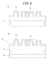
- FIG. FIG. 5 is a process diagram for explaining an example of a method for manufacturing the photodetector of the first embodiment.
- FIG. 5 is a process diagram for explaining an example of a method for manufacturing the photodetector of the first embodiment.
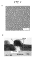
- 2 is an electron microscope image of the photodetector of Example 1.
- FIG. 6 is a cross-sectional view illustrating a schematic configuration of a photodetector according to Example 2.
- FIG. 6 is a cross-sectional view illustrating a schematic configuration of a photodetector according to Example 3.
- FIG. 6 is a cross-sectional view illustrating a schematic configuration of a photodetector according to Embodiment 4.
- FIG. It is a schematic perspective view which shows the modification of the photodetector which concerns on this invention.
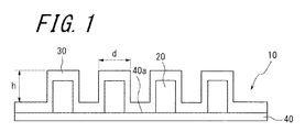
- FIG. 1 is a cross-sectional view showing the basic configuration of a photodetector according to the present invention.
- the photodetector 10 according to the present invention includes an organic semiconductor 20, a metal layer 30, and a semiconductor 40.
- the organic semiconductor 20 is formed in a plurality of convex shapes on the semiconductor 40, and constitutes a concavo-convex structure having a convex portion and a concave portion adjacent to the convex portion together with the semiconductor 40.
- the metal layer 30 is added on the organic semiconductor 20 and the semiconductor 40 having a concavo-convex structure, and promotes plasmon resonance of at least one of localized plasmon resonance and surface plasmon resonance by irradiation with detection light.
- the height h of the convex part of the concavo-convex structure including the metal layer 30, that is, the width in the vertical direction between the convex part and the concave part of the metal layer 30, is a dimension equal to or smaller than the wavelength of the detection light and the thickness of the convex part. That is, the maximum dimension d in a plane orthogonal to the straightening direction (height direction) of the convex portion is equal to or less than the wavelength of the detection light.
- the height h of the convex portion is more preferably 1/10 to 1/5 of the detection wavelength.
- localized plasmons can be excited efficiently (for example, JJ Mock, M. Barbic, DR Smith, DA Schultz, and S.
- the convex portion may be formed in an arbitrary shape such as a columnar shape or a prismatic shape, and may be formed regularly or may be formed in an irregular manner.
- the semiconductor 40 is composed of an organic semiconductor or an inorganic semiconductor, and allows electrons excited by plasmon resonance in the metal layer 30 to pass through the junction 40 a with the metal layer 30.
- the semiconductor 40 is preferably supported on a substrate.
- FIGS. 2A to 2D are diagrams for explaining the operation of the photodetector 10 in FIG.
- the wavelength of the incident light and the size of the concavo-convex structure are matched to generate localized plasmon resonance and / or surface plasmon resonance.
- the electron of the metal layer 30 is excited.
- the amount of electrons excited by this plasmon resonance is greater than when the plasmon resonance is not excited, that is, when the incident light is totally reflected.
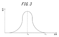
- FIG. 3 is a diagram illustrating the relationship between the wavelength of incident light and the detection current in the photodetector 10.
- the organic semiconductor 30 since the organic semiconductor 30 is used, it can be easily manufactured and integrated. Further, by appropriately setting the size of the concavo-convex structure, the absorption wavelength ⁇ m in FIG. 3 can be changed, so that the light detection wavelength can be tuned. Further, in FIG. 2C, the electrons excited by the metal layer 30 get over the barrier of the junction 40a, so that the wavelength band ( ⁇ e in FIG. 3) of the light to be detected is tuned by tuning the barrier. be able to.
- the semiconductor 40 is made of an organic semiconductor
- the material selectivity is higher than when the semiconductor 40 is made of an inorganic semiconductor. Since the organic semiconductor 30 is formed in a convex shape (columnar shape), light in the infrared region can be detected with high sensitivity without depending on the incident angle.
- the organic semiconductor 20 is not limited to CuPc, and may be composed of other phthalocyanine-based materials, thiophene-based materials, or Alq3.
- the photodetector is composed of the materials shown in Table 2.
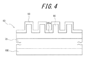
- FIG. 4 is a cross-sectional view illustrating a schematic configuration of the photodetector according to the first embodiment.
- an organic semiconductor part 80 made of PTCDA / CuPc constituting the organic semiconductor 20 and the semiconductor 40 of FIG. 1 is formed on the surface of a silicon substrate 70 that is an inorganic semiconductor.
- An Au layer 90 constituting the metal layer 30 of FIG. 1 is formed on the surface of the concavo-convex structure.
- an Al layer 100 for taking out an output current is formed on the back surface of the silicon substrate 70.
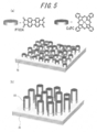
- FIG. 5 and 6 are process diagrams for explaining an example of a manufacturing method of the photodetector 60 of FIG.
- two types of organic semiconductors PTCDA / CuPc
- Vapor deposition was performed to a thickness corresponding to 3 nm.
- PTCDA plays a role of identifying a site where CuPc forming the convex portion grows.
- the silicon substrate 70 was heated at 80 ° C. to 230 ° C. for 1 hour, and as shown in FIG.
- CuPc was crystal-grown to form an organic semiconductor portion 80 having a concavo-convex structure.
- illustration of CuPc formed on the silicon substrate 70 in the concave portion of the concave-convex structure is omitted.
- the photo detector 60 was completed.
- FIG. 7 shows an electron microscope image of the photodetector 60 produced as described above.
- A shows a surface image of the concavo-convex structure of the photodetector 60 by a scanning electron microscope (SEM).
- B shows the cross-sectional image of the photodetector 60 by a transmission electron microscope (TEM).
- FIG. 7 is an electron microscope image of the photodetector 60 when the organic semiconductor part 80 is formed by heating the silicon substrate 70 at 200 ° C. for 1 hour to grow a crystal of CuPc.
- nano-sized convex portions are erected on the surface of the photodetector 60.
- the Au layer 90 is formed so as to surround the convex portion of the organic semiconductor portion 80.
- the Au layer 90 and the silicon substrate 70 are not in direct contact with each other, and the organic semiconductor layer constituting the organic semiconductor portion 80 is 10 nm or less in thickness between them. It can be seen that they are interposed.
- corrugated structure of the photodetector 60 ie, the depth of a recessed part, is 50 nm or more.
- the photodetector 60 in this case was observed. It was found that the height of the convex part of the concavo-convex structure was 20 nm or more.
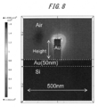
- Fig. 8 shows an analysis photograph of the calculation model and the calculation result of the electric field strength distribution.
- the calculation model has a structure in which an Au thin film with a thickness of 50 nm is deposited on a silicon substrate, and a convex portion of Au with a width of 50 nm and a height of h nm stands at the center. For simplicity, organic semiconductors were excluded from the calculation. Since the periodic boundary condition is applied as the boundary condition in the direction of the side surface of the convex portion, in the case of FIG. 8, the structure is such that the convex portion stands on the Au thin film so as to fill the plane with a pitch of 500 nm.
- TM Transverse Magnetic
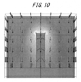
- FIG. 8 shows that an electric field intensity distribution is generated around the convex portion when resonance occurs, suggesting that a dipole-like plasmon mode is excited.
- the electric field strength distribution was analyzed by vector display.
- FIG. 10 is an analysis photograph showing the electric field strength distribution. From FIG. 10, it was found that the electric field starting from the tip of the convex portion is perpendicularly incident on the substrate surface and terminates. This is because the convex part is formed upright from the surface of the Au thin film, so that a negative charge is induced at the position of the mirror image inside the substrate, and this may form a dipole-shaped electric field intensity distribution in the upper half. is there.
- FIG. 11 is an analysis photograph visualizing the current distribution in this case. From FIG. 11, it can be seen that the current flows toward the tip of the convex portion. This suggested that the charge density at the tip of the convex portion was increased.
- the light absorption / detection may be promoted by the plasmon resonance of the surface structure.
- Example 1-1 shows a photodetector 60 in which a silicon substrate 70 is heated at 200 ° C. to form an organic semiconductor portion 80 having a concavo-convex structure.
- Example 1-2 shows a photodetector 60 in which the silicon substrate 70 is heated at 110 ° C. to form the organic semiconductor portion 80 having a concavo-convex structure.
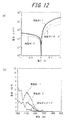
- FIG. 12A also shows a measurement result of a reference diode (Au thickness is 50 nm) made of an Au / n-type silicon junction without a concavo-convex structure as a reference device.
- the parameter is “Guiding Liang, Tianhong Cui, Kody Varahramyan,“ Fabrication and electrical charactaristics of polymer-based Schottky diode 3 ”, which is based on“ Sol 69-Sol 69 ”.
- the present inventors evaluated the spectral sensitivity characteristics of the photodetector 60.
- a source meter (2400 manufactured by Keithley) was used, and current detection was performed with an applied voltage of 0 V (that is, during a short circuit). The result is shown in FIG.
- Example 1-1 is 1.79 mA / W
- Example 1-2 is 0.945 mA / W
- the reference diode is 0. 141 mA / W. From this result, it was found that the sensitivity at this wavelength increases when the uneven structure exists. Specifically, in the case of Example 1-1, it was confirmed that the sensitivity was improved by about 12.7 times that of the reference diode by one digit or more. Moreover, in the case of Example 1-2, the sensitivity improvement about 6.7 times with respect to the reference diode was confirmed.
- the present embodiment it is possible to obtain a photodetector that can be easily manufactured and can detect light in the infrared region with high sensitivity without depending on the incident angle.
- the highly versatile silicon substrate 70 since the highly versatile silicon substrate 70 is used, the cost can be reduced, the integration is facilitated, and the applicability can be expanded.
- FIG. 13 is a cross-sectional view illustrating a schematic configuration of the photodetector according to the second embodiment.
- the photodetector 61 of this embodiment is obtained by changing the silicon substrate 70 and the Al layer 100 to the conductive substrate 71 in the photodetector 60 of FIG.
- the conductive substrate 71 is formed by vapor-depositing a transparent electrode (ITO: Indium Tin Oxide) 73 on the polyimide substrate 72, and the organic semiconductor portion 80 is formed on the transparent electrode 73. Since other configurations are the same as those in FIG. 4, the same reference numerals are given to the same components as those in FIG. 4, and description thereof will be omitted.
- ITO Indium Tin Oxide
- the electrons excited in the Au layer 90 by the localized plasmon resonance and / or the surface plasmon resonance overcome the Schottky barrier at the junction 80 a between the Au layer 90 and the organic semiconductor portion 80. Injected into.
- the electrons injected into the organic semiconductor unit 80 are taken out through the transparent electrode 73 of the conductive substrate 71.
- a conductive substrate 71 is formed by forming a transparent electrode 73 by vapor-depositing a transparent oxide material (ITO) on a commercially available polyimide substrate 72. Thereafter, an organic semiconductor portion 80 having a concavo-convex structure made of PTCDA / CuPc is formed on the transparent electrode 73 in the same manner as in the first embodiment, and Au is further deposited on the concavo-convex side of the organic semiconductor portion 80 to form an Au layer 90.
- the photodetector 61 is manufactured.
- the conductive substrate 71 is not limited to ITO / polyimide, and can be formed of a flexible conductive substrate such as ITO / PET (polyethylene terephthalate) or aluminum foil. Therefore, in addition to the same effects as those of the first embodiment, a flexible sensor can be realized, and development for ubiquitous applications is possible.
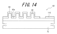
- FIG. 14 is a cross-sectional view illustrating a schematic configuration of the photodetector according to the third embodiment.
- the photodetector 62 of the present embodiment is obtained by changing the silicon substrate 70 and the Al layer 100 to the glass substrate 75 and the metal joint 110 which are insulating substrates in the photodetector 60 of FIG.
- the metal bonding part 110 is made of platinum (Pt), for example, and is formed by ohmic bonding to a part of the organic semiconductor part 80. Since other configurations are the same as those in FIG. 4, the same reference numerals are given to the same components as those in FIG. 4, and description thereof will be omitted.
- the electrons excited in the Au layer 90 by the localized plasmon resonance and / or the surface plasmon resonance overcome the Schottky barrier at the junction 80 a between the Au layer 90 and the organic semiconductor portion 80. Injected into. Then, the electrons injected into the organic semiconductor unit 80 are taken out through the metal junction 110.
- the photodetector 62 of FIG. 14 In manufacturing the photodetector 62 of FIG. 14, first, similarly to the case of Example 1, an uneven semiconductor structure 80 made of PTCDA / CuPc is formed on the glass substrate 75, and the organic semiconductor section Au is vapor-deposited on the concavo-convex side of 80 to form an Au layer 90. Then, the photodetector 62 is produced by vapor-depositing the metal bonding part 110 on a part of the organic semiconductor part 80 and performing ohmic bonding.
- the present embodiment can be surface-mounted on an insulating substrate such as a glass substrate 75, an effect of increasing the applicability of the system can be obtained, for example, it can be directly mounted on a windshield of a car.
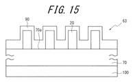
- FIG. 15 is a cross-sectional view illustrating a schematic configuration of the photodetector according to the fourth embodiment.
- the photodetector 63 of this embodiment is obtained by forming the organic semiconductor 20 in a convex shape (columnar shape) directly on the silicon substrate 70 in the photodetector 60 of FIG. That is, the semiconductor 40 of FIG. Therefore, in this embodiment, since the Au layer 90 comes into contact with the organic semiconductor 20 and the silicon substrate 70, electrons excited in the Au layer 90 by localized plasmon resonance and / or surface plasmon resonance are Au Overcoming the Schottky barrier at the junction 70 a between the layer 90 and the silicon substrate 70, the silicon layer 70 is taken out from the Al layer 100.
- the substrate temperature of the silicon substrate 70 and the deposition conditions of PTCDA / CuPc constituting the organic semiconductor 20 are optimized, and the convex organic semiconductor 20 on the silicon substrate 70 is obtained. Forming a part where is present and a part not existing. Thereafter, the Au layer 90 is vapor-deposited on the organic semiconductor 20 side of the silicon substrate 70, and the Al layer 100 is vapor-deposited on the opposite side, whereby the photodetector 63 is manufactured.
- the spectral response was measured using a source meter in the same manner as in Example 1.
- this invention is not limited to the said Example, A various deformation
- a plurality of columnar convex portions of the concavo-convex structure including the metal layer 30 are curved or bent at an arbitrary curvature or angle, It may be formed in an arbitrary shape.
- the height h of the convex portion of the concavo-convex structure including the metal layer 30, that is, the width in the vertical direction between the convex portion and the concave portion of the metal layer 30, is the same as that of the photodetector according to the present invention described above.
- the dimension below the wavelength of the detection light, more preferably 1/10 to 1/5 of the detection wavelength, and the thickness of the convex part, that is, the maximum dimension d in the cross section perpendicular to the height direction of the convex part is the wavelength of the detection light.
Landscapes
- Physics & Mathematics (AREA)
- Electromagnetism (AREA)
- Chemical & Material Sciences (AREA)
- Inorganic Chemistry (AREA)
- Engineering & Computer Science (AREA)
- Materials Engineering (AREA)
- Spectroscopy & Molecular Physics (AREA)
- Light Receiving Elements (AREA)
- Photometry And Measurement Of Optical Pulse Characteristics (AREA)
Abstract
凸部を有する有機半導体20と、有機半導体20上に付加され、検出光の照射により電子が励起される局在プラズモン共鳴及び表面プラズモン共鳴の少なくとも一方のプラズモン共鳴を促進する金属層30と、金属層30に接合され、プラズモン共鳴により励起される電子を金属層30との接合部40aにおいて通過させる半導体40と、を備える。
Description
本出願は、2013年5月23日に日本国に特許出願された特願2013−109015の優先権を主張するものであり、この先の出願の開示全体をここに参照のために取り込む。
本発明は、光検出器に関するものである。
近年、光検出器として、量子井戸構造を有するもの(例えば、非特許文献1参照)、量子井戸の代わりに金属(Au)/半導体材料(Ge)を用いた赤外光吸収体(メタマテリアル型)を有するもの(例えば、非特許文献2参照)、シリコンを用いた金属半導体接合を利用したもの(例えば、非特許文献3参照)、表面プラズモン共鳴を発生させるアンテナ層を備えるもの(例えば、特許文献1参照)、などが提案されている。
Altin,E.,M.Hostut,and Y.Ergun."Dark current and optical properties in asymmetric GaAs/AlGaAs staircase−like multi quantum well structure."Infrared Physics & Technology(2013)
Yanxia Cui,Kin Hung Fung,Jun Xu,Hyungjin Ma,Yi Jin,Sailing He,and Nicholas X.Fang,"Ultrabroadband Light Absorption by a Sawtooth Anisotropic Metamaterial Slab",Nano letters,Vol.12,No.3,pp.1443~1447(2012)
Casalino,M.;Sirleto,L.;Moretti,L.& Rendina,"A silicon compatible resonant cavity enhanced photodetector working at 1.55μm.",Semicond.Sci.Technol.,Vol.23,No.7,pp.075001(2008)
しかしながら、非特許文献1に開示の光検出器は、化合物半導体を使用するため、シリコンプロセスとの親和性に欠けるものである。つまり、化合物半導体の材料制御は、きめ細かく、かつ、高温で行う必要があるため、真空チャンバー内のコンタミネーション(汚染物)が存在すると、汚染物の拡散により材料の組成が変化し、所望の材料が得られないことになる。そのため、シリコンデバイスに、これらの光検出器を製膜等のプロセスを用いてインテグレーションするのは困難となることが想定される。したがって、シリコンデバイスを用いて量子井戸を形成することを考えると、結晶シリコンとアモルファスシリコンとの積層作成は、通常の蒸着プロセスでは理論上不可能とある。その理由は、結晶シリコンを得るには、アモルファスシリコンを高温でアニールして再結晶化するプロセスが必要となるからである。
非特許文献2に開示の光検出器は、金属のプラズモニックな共鳴を利用して、赤外光を吸収するものであるが、作製が困難であることが想定される。その理由としては、上述した金属のコンタミネーションの問題があることが挙げられる。
非特許文献3に開示の光検出器は、シリコンを用いた金属半導体接合を利用するので、非特許文献1、2に開示の光検出器と比較して、容易に作製することが可能である。しかしながら、シリコンは赤外線領域の光の検出感度が低いため、検出光の波長が制限されることになる。
特許文献1に開示の光検出器は、アンテナ層で発生する表面プラズモン共鳴により、アンテナ層の貫通孔から近接場光を出力させ、その近接場光を貫通孔部分の受光面を介して受光層で受光するものである。したがって、かかる光検出器によると、所望の波長の光により表面プラズモン共鳴が生じるようにアンテナ層を適切に構成することで、赤外線領域の光をも検出することが可能となる。しかしながら、かかる光検出器においては、アンテナ層がグレーティング構造からなるため、検出感度に入射角依存性を有することになり、広範囲の入射角に亘って安定した検出感度が得られないことになる。
したがって、上述した観点に鑑みてなされた本発明の目的は、容易に製作でき、入射角に依存することなく赤外線領域の光をも高感度で検出できる光検出器を提供することにある。
上記目的を達成する本発明に係る光検出器は、
凸部を有する有機半導体と、
前記有機半導体上に付加され、検出光の照射により電子が励起される局在プラズモン共鳴及び表面プラズモン共鳴の少なくとも一方のプラズモン共鳴を促進する金属層と、
前記金属層に接合され、前記プラズモン共鳴により励起される電子を前記金属層との接合部において通過させる半導体と、
を備える。
かかる構成によると、プラズモン共鳴によって励起される電子が多くなることから検出感度の向上が図れる。また、有機半導体を容易に製作でき、入射角に依存することなく赤外線領域の光をも高感度で検出することが可能となる。
凸部を有する有機半導体と、
前記有機半導体上に付加され、検出光の照射により電子が励起される局在プラズモン共鳴及び表面プラズモン共鳴の少なくとも一方のプラズモン共鳴を促進する金属層と、
前記金属層に接合され、前記プラズモン共鳴により励起される電子を前記金属層との接合部において通過させる半導体と、
を備える。
かかる構成によると、プラズモン共鳴によって励起される電子が多くなることから検出感度の向上が図れる。また、有機半導体を容易に製作でき、入射角に依存することなく赤外線領域の光をも高感度で検出することが可能となる。
前記金属層を含む凸部の高さは、前記検出光の波長以下の寸法で、該凸部の太さの最大寸法が前記検出光の波長以下の寸法とするとよい。これにより、プラズモン共鳴をより効率よく促進させることが可能となる。
前記半導体は、有機半導体としてもよい。これにより、金属層との接合部のショットキー障壁のチューニングが可能となることから、障壁を乗り越えられる電子量を多くでき、感度の向上が図れるとともに、感度帯域のチューニングも可能となる。
さらに、前記半導体を支持する基板を備えるとよい。これにより、種々の実装が可能となる。
前記基板は、半導体基板としてもよい。これにより、シリコンなどの汎用性の高い基板を用いることができ、コストダウンが図れるとともに、集積化が容易にでき、応用性を広げることが可能となる。
前記基板は、導電性基板としてもよい。これにより、ITO/PET、ITO/ポリイミド、アルミホイルなどのフレキシブルな導電性基板を用いることができ、フレキシブルな光検出器を実現することが可能となる。
前記基板は、絶縁性基板としてもよい。これにより、ガラスなどの絶縁性基板上に表面実装でき、応用性の拡大が図れる。
前記半導体は、無機半導体であってもよい。これにより、プラズモン共鳴による光吸収を促す作用を実現することができる。
前記金属層を含む凸部の高さは、20nm以上とするとよい。これにより、凸部のない光検出器と比較して、約6倍の検出感度向上を実現できる。
前記金属層を含む凸部の高さは、50nm以上とするとよい。これにより、凸部のない光検出器と比較して、一桁以上の検出感度向上を実現できる。
前記金属層は、凸部と該凸部に隣接する凹部とを有する凹凸構造であって、
前記凹凸構造の凸部の高さは、前記検出光の波長以下の寸法で、かつ該凸部の太さの最大寸法が前記検出光の波長以下の寸法であってもよい。
前記凹凸構造の凸部の高さは、前記検出光の波長以下の寸法で、かつ該凸部の太さの最大寸法が前記検出光の波長以下の寸法であってもよい。
前記金属層を含む凸部は、任意の形状に湾曲又は屈曲して形成されてもよい。これによい、製作がより容易になる。
前記有機半導体は、フタロシアニン系、チオフェン系、Alq3のいずれかとしてもよい。
前記金属層は、Au、Pt、Al、Agのいずれかとしてもよい。
前記半導体は、フタロシアニン系、チオフェン系、Alq3、シリコンのいずれかとしてもよい。
本発明によれば、容易に製作でき、入射角に依存することなく赤外線領域の光をも高感度で検出できる光検出器を得ることができる。
先ず、本発明に係る光検出器の原理について説明する。
図1は、本発明に係る光検出器の原理的構成を示す断面図である。本発明に係る光検出器10は、有機半導体20と、金属層30と、半導体40とを備える。有機半導体20は、半導体40上に凸状に複数形成されて、半導体40とともに凸部と該凸部に隣接する凹部とを有する凹凸構造を構成する。金属層30は、凹凸構造の有機半導体20及び半導体40上に付加されて、検出光の照射により局在プラズモン共鳴及び表面プラズモン共鳴の少なくとも一方のプラズモン共鳴を促進する。したがって、金属層30を含む凹凸構造の凸部の高さh、つまり金属層30の凸部と凹部との垂直方向の幅は、検出光の波長以下の寸法で、かつ凸部の太さ、つまり凸部の伸直方向(高さ方向)と直交する平面内における最大寸法dは検出光の波長以下となっている。なお、凸部の高さhは、検出波長の1/10~1/5がより好ましい。この場合には、局在プラズモンを効率よく励起させることができる(例えば、J.J.Mock,M.Barbic,D.R.Smith,D.A.Schultz,and S.Schultz, “Shape effects in plasmon resonance of individual colloidal silver nanoparticles”,J.Chem.Phys.116,6755(2002)参照)。また、凸部は、円柱状、角柱状等の任意の形状で、規則的に形成されていても、不規則に林立して形成されていてもよい。
半導体40は、有機半導体又は無機半導体で構成され、金属層30でのプラズモン共鳴により励起される電子を金属層30との接合部40aにおいて通過させる。なお、半導体40は、好ましくは基板上に支持される。
図2(a)~(d)は、図1の光検出器10の作用を説明するための図である。先ず、図2(a)に示すように、凹凸構造の金属30に光が入射すると、入射光の波長と凹凸構造の大きさとが整合して、局在プラズモン共鳴及び/又は表面プラズモン共鳴が生じる。これにより、図2(b)に示すように、金属層30の電子が励起される。このプラズモン共鳴によって励起され電子の量は、プラズモン共鳴が励起されない場合、つまり入射光が全反射される場合と比較して多い。
金属層30に励起された電子は、図2(c)に示すように、金属層30と半導体40との接合部40aを通過する。ここで、接合部40aには、金属と半導体との接触により電界が形成されているので、励起された電子は、接合部40aの金属/半導体のショットキー障壁を乗り越えられた電子が拡散電流として流れる。したがって、図2(d)に示すように、半導体40に流れる電流を電流計等の電流検出部50で検知することにより、入射光を検出することができる。なお、接合部40aにおける金属/半導体界面の電界を急峻にするために、接合部40aに電位を印加してもよい。図3は、光検出器10における入射光の波長と検出電流との関係を示す図である。
図1に示した光検出器10によると、有機半導体30を用いるので、製作及び集積化が容易にできる。また、凹凸構造のサイズを適切に設定することにより、図3の吸収波長λmを変更できるので、光検出波長のチューニングが可能となる。また、図2(c)において、金属層30に励起された電子は、接合部40aの障壁を乗り越えるので、障壁をチューニングすることにより、検出する光の波長帯域(図3のλe)をチューニングすることができる。特に、半導体40を有機半導体で構成する場合は、無機半導体で構成する場合よりも材料の選択性が多いので、障壁を制御し易い効果がある。有機半導体30を凸状(柱状)に形成することから、入射角に依存することなく赤外線領域の光をも高感度で検出することが可能となる。
ここで、上述した光検出器10を構成する有機半導体20、金属層30及び半導体40、並びに半導体40を支持する基板としては、例えば、表1に示す材料から任意の組み合わせが可能であるが、これに限定されるものではない。例えば、有機半導体20は、CuPcに限らず、他のフタロシアニン系で構成したり、チオフェン系やAlq3で構成したりしてもよい。

表1において、例えば、金属層30をAl、有機半導体20をCuPc、半導体40及び基板をシリコンとした場合、Alの仕事関数(4.1eV)と、シリコンの電子親和力(4.15eV)との差が障壁高さ(0.05eV)となるため、検出光の波長λは、λ=20μm以下となる。さらに、表1の選択を最適化し、障壁高さを小さくすることにより、検出光の波長を大きくしてもよい。
以下、本発明の実施例について説明する。なお、以下の実施例においては、光検出器を表2に示す材料で構成するものとする。
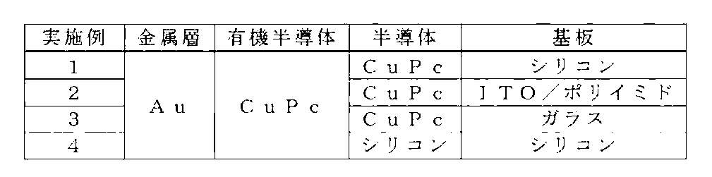
図4は、実施例1に係る光検出器の概略構成を示す断面図である。図4の光検出器60は、無機半導体であるシリコン基板70の表面に、図1の有機半導体20及び半導体40を構成するPTCDA/CuPcからなる有機半導体部80が形成され、この有機半導体部80の凹凸構造の表面に図1の金属層30を構成するAu層90が形成されている。また、シリコン基板70の裏面には、出力電流を取り出すためのAl層100が形成されている。
図4の光検出器60において、凹凸構造のAu層90に光が入射すると、局在プラズモン共鳴及び/又は表面プラズモン共鳴が生じて、Au層90の電子が励起される。Au層90で励起された電子は、Au層90と有機半導体部80との接合部80aのショットキー障壁を乗り越えて有機半導体部80に注入され、シリコン基板70を経てAl層100から取り出される。
図5及び図6は、図4の光検出器60の製造方法の一例を説明するための工程図である。先ず、図5(a)に示すように、面方位<100>、比抵抗ρ=40Ωcmのn型単結晶のシリコン基板70の表面に、二種類の有機半導体(PTCDA/CuPc)を、それぞれ例えば3nmに相当する厚さに蒸着した。PTCDAは、凸部を形成するCuPcが成長する部位を同定する役割を果たすものである。その後、シリコン基板70を80℃~230℃で1時間加熱して、図5(b)に示すように、CuPcを結晶成長させて凹凸構造を有する有機半導体部80を形成した。なお、図5(b)では、凹凸構造の凹部のシリコン基板70上に形成されるCuPcの図示を省略している。
次に、真空蒸着装置(真空度=1.0×10⁻⁴Pa)により、図6(a)に示すように、有機半導体部80の凹凸構造の表面にAuを蒸着してAu層90を形成した。そして、最後に、真空蒸着装置(真空度=4.0×10⁻²Pa)により、図6(b)に示すように、シリコン基板70の裏面にAlを蒸着してAl層100を形成し、光検出器60を完成させた。
図7は、上述したようにして作製された光検出器60の電子顕微鏡画像を示すもので、(a)は走査型電子顕微鏡(SEM)による光検出器60の凹凸構造の表面像を示し、(b)は透過型電子顕微鏡(TEM)による光検出器60の断面像を示す。なお、図7は、シリコン基板70を200℃で1時間加熱してCuPcを結晶成長させて有機半導体部80を形成した場合の光検出器60の電子顕微鏡画像である。
図7(a)から明らかなように、光検出器60の表面には、ナノサイズの凸部が林立していることが分かる。また、図7(b)から明らかなように、有機半導体部80の凸部を取り囲むように、Au層90が成膜されていることが分かる。さらに、図7(b)から明らかなように、Au層90とシリコン基板70とは直接接しておらず、これらの間には有機半導体部80を構成する有機半導体層が10nm以下の厚さで介在していることが分かる。また、光検出器60の凹凸構造の凸部の高さすなわち凹部の深さは、50nm以上であることが分かる。なお、シリコン基板70を110℃で1時間加熱してCuPcを結晶成長させて有機半導体部80を形成し、同様にして光検出器60を作成して観察したところ、この場合の光検出器60の凹凸構造の凸部の高さは、20nm以上であることが分かった。
次に、本実施例に係る光検出器60によるプラズモン吸収作用について、本発明者らが行った検証について説明する。この検証は、汎用物理シミュレーションソフトである「COMSOL Multiphysics」(商品名)を用い、凹凸構造の電磁界シミュレーションを試みたものである。つまり、Auの凸部が林立している基板上に光を照射し、近赤外領域に吸収ピークが存在するかを確認したものである。
図8に計算モデルと電界強度分布の計算結果との解析写真を示す。計算モデルは、シリコン基板上に厚さ50nmのAu薄膜が蒸着されており、中央部に幅50nm、高さhnmのAuの凸部が立っている構造である。簡単のため、有機半導体は計算から除外した。境界条件として、凸部側面方向に周期境界条件を適用したので、図8の場合であれば、Au薄膜上に500nmピッチで平面を埋め尽くすように凸部が林立している構造となる。ここでは、凸部の高さh及び凸部のピッチに対して、上面側から垂直にTM(Transverse Magnetic)波を入射して、反射率R及び透過率Tから1−T−R計算によって基板表面による吸収率を計算した。
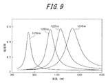
図9は、この場合の異なる高さhに対する吸収率スペクトルを示す図である。図9から、h=150nm~250nmの凸部が、赤色可視光領域から1500nmの波長領域において、シングルピークの共鳴点で吸収が増大していることが判明した。なお、図9における凸部のピッチは400nmに対応している。
この結果は、凹凸構造の形状が、吸収波長(図3のλm)を決定することを示している。また、図8から、共鳴が生じているときに凸部周囲に電界強度分布が生じているのが認められ、ダイポール的なプラズモンモードが励起されていることが示唆される。実際に吸収ピークにおける振動がダイポール的な応答かを調べるために、電界強度分布をベクトル表示して解析した。
図10は、電界強度分布を示す解析写真である。図10から、凸部の先端を起点とする電界が、基板表面に垂直に入射して終端していることがわかった。これは、凸部がAu薄膜表面から直立して形成されているため、基板内部の鏡像の位置に負電荷が誘起され、これにより上半分のダイポール状の電界強度分布が形成される可能性がある。
図11は、この場合の電流分布を可視化した解析写真である。図11から、電流が凸部の先端部に向かって流れていることがわかる。これにより、凸部先端の電荷密度が上昇していることが示唆された。
以上の解析により、共鳴時においては凸部先端に電荷分布が発生し、ダイポール状のプラズモンモードが励起されていることが分かった。したがって、本実施例に係る光検出器60は、光吸収・検出が表面構造のプラズモン共鳴によって促進されている可能性がある。
また、本発明者らは、光検出器60の効果を確認するために、その電気的特性を取得した。まず、光検出器60のAu層90を正極、n型のシリコン基板70側を負極にとって、電流・電圧特性を取得した。その結果を図12(a)に示す。図12(a)において、実施例1−1は、シリコン基板70を200℃で加熱して凹凸構造の有機半導体部80を形成した光検出器60を示す。また、実施例1−2は、シリコン基板70を110℃で加熱して凹凸構造の有機半導体部80を形成した光検出器60を示す。なお、図12(a)には、参照用のデバイスとして、凹凸構造のないAu/n型シリコン接合からなる参照ダイオード(Auの厚さは50nm)の測定結果も示している。
図12(a)の結果から、順方向に流れるキャリアは電子であることが言える(Sze S M 1981 Physics of Semiconductor Devices 2nd edn(NewYork:Wiley)参照)。また、これらのダイオードの寄生抵抗Rs、ショットキー障壁高さΦb及びn値を求めることは、ダイオードの特長を知る上で重要である。特にショットキー障壁高さΦbについては、赤外光センサの検出帯域を決定する重要なパラメータである。そこで、これらのパラメータを求めた。その結果を表3に示す。なお、パラメータは、「Guirong Liang,Tianhong Cui,Kody Varahramyan,” Fabrication and electrical characteristics of polymer−based Schottky diode” Solid−State Electronics 47(2003)691?694」記載の方法に基づいて算出したものである。

表3から明らかなように、実施例1−1、1−2と凹凸構造を有しない参照ダイオードとを比較すると、(1)寄生抵抗Rsについては、実施例1−1、1−2の光検出器60の方が低く、(2)ショットキー障壁高さΦbについては、殆ど変わらないことが分かる。(1)については、Auとn型シリコンとの接触面積よりも、Auと凹凸構造を形成している有機半導体との接触面積が大きくなり、電流経路が増えたためと想定される。一方、(2)については、実施例1−1、1−2の光検出器60を赤外線センサとして用いる場合、検出帯域は参照ダイオードの検出帯域と殆ど変わらないことが考えられる。また、n値については、いずれも1.5以下である。これは、実施例1−1、1−2の光検出器60の支配的な駆動電流が拡散電流であることから、欠陥の少ない良好なダイオード動作を実現していることを示している。
さらに、本発明者らは、光検出器60の分光感度特性の評価を行った。この評価では、波長の長い領域の評価を行うため、波長領域λをλ=1000nm~1500nmに絞って感度の評価を行った。なお、電流検出については、ソースメータ(ケースレー社製2400)を用い、印加電圧は0V(つまり、短絡時)の電流検出を行った。その結果を図12(b)に示す。
図12(b)において、λ=1200nmでの感度特性について比較すると、実施例1−1が1.79mA/Wであり、実施例1−2が0.945mA/Wであり、参照ダイオードは0.141mA/Wであった。この結果から、凹凸構造が存在すると、本波長での感度が高くなることが分かった。具体的には、実施例1−1の場合、参照ダイオードに対して約12.7倍の一桁以上の感度向上が確認できた。また、実施例1−2の場合、参照ダイオードに対して約6.7倍の感度向上が確認できた。この波長(λ=1200nm)を持つ光のエネルギー(hν=1.03eV)は、シリコンのバンドギャップ(Eg=1.12eV)以下であるため、この波長での光吸収はAu層90で行われているものと考えられる。これにより、この波長での凹凸構造を有するダイオードの感度は、参照ダイオードの感度と比較して大きくなっていることから、Au層90での吸収が大きくなっていることが言える。
以上のことから、本実施例によれば、容易に製作でき、入射角に依存することなく赤外線領域の光をも高感度で検出できる光検出器を得ることができる。また、汎用性の高いシリコン基板70を用いることから、コストダウンが図れるとともに、集積化が容易になり、応用性を広げることが可能となる。
図13は、実施例2に係る光検出器の概略構成を示す断面図である。本実施例の光検出器61は、図4の光検出器60において、シリコン基板70及びAl層100を導電性基板71に変更したものである。導電性基板71は、ポリイミド基板72上に透明電極(ITO:Indium Tin Oxide)73を蒸着して形成され、透明電極73上に有機半導体部80が形成されている。その他の構成は図4と同様であるので、図4と同様の構成要素には、同一参照符号を付して説明を省略する。
本実施例において、局在プラズモン共鳴及び/又は表面プラズモン共鳴によってAu層90に励起された電子は、Au層90と有機半導体部80との接合部80aのショットキー障壁を乗り越えて有機半導体部80に注入される。そして有機半導体部80に注入された電子は、導電性基板71の透明電極73を経て取り出される。
図13の光検出器61を製造するにあたっては、先ず、市販のポリイミド基板72上に、透明酸化物材料(ITO)を蒸着して透明電極73を形成して導電性基板71を作成する。その後、透明電極73上に、実施例1の場合と同様に、PTCDA/CuPcから成る凹凸構造の有機半導体部80を作成し、さらに有機半導体部80の凹凸側にAuを蒸着してAu層90を形成することで、光検出器61が作製される。
本実施例の光検出器61について、実施例1と同様に、ソースメータを用いて分光感度特性を測定した。その結果、赤外領域(λ=1200nm)において光応答を確認することができた。また、本実施例において、導電性基板71は、ITO/ポリイミドに限らず、ITO/PET(ポリエチレンテレフタレート)やアルミホイルなどのフレキシブルな導電性基板で構成することができる。したがって、実施例1と同様の効果が得られる他、フレキシブルなセンサが実現でき、ユビキタス的な用途への展開が可能となる。
図14は、実施例3に係る光検出器の概略構成を示す断面図である。本実施例の光検出器62は、図4の光検出器60において、シリコン基板70及びAl層100を絶縁性基板であるガラス基板75及び金属接合部110に変更したものである。金属接合部110は、例えば白金(Pt)からなり、有機半導体部80の一部にオーミック接合して形成される。その他の構成は図4と同様であるので、図4と同様の構成要素には、同一参照符号を付して説明を省略する。
本実施例において、局在プラズモン共鳴及び/又は表面プラズモン共鳴によってAu層90に励起された電子は、Au層90と有機半導体部80との接合部80aのショットキー障壁を乗り越えて有機半導体部80に注入される。そして有機半導体部80に注入された電子は、金属接合部110を経て取り出される。
図14の光検出器62を製造するにあたっては、先ず、ガラス基板75上に、実施例1の場合と同様に、PTCDA/CuPcから成る凹凸構造の有機半導体部80を作成し、さらに有機半導体部80の凹凸側にAuを蒸着してAu層90を形成する。その後、有機半導体部80の一部に金属接合部110を蒸着してオーミック接合することで、光検出器62が作製される。
本実施例の光検出器62について、Au層90側を正極、金属接合部110側を負極として、実施例1と同様に、ソースメータを用いて分光感度特性を測定した。その結果、赤外領域(λ=1200nm)において光応答を確認することができた。したがって、実施例1と同様の効果が得られる。また、本実施例は、ガラス基板75などの絶縁性基板に表面実装できるので、例えば車のフロントガラス等に直接実装できるなど、システムの応用性が増大する効果が得られる。
図15は、実施例4に係る光検出器の概略構成を示す断面図である。本実施例の光検出器63は、図4の光検出器60において、シリコン基板70上に直接、有機半導体20を凸状(柱状)に形成したものである。すなわち、図1の半導体40を、シリコン基板70としたものである。したがって、本実施の形態においては、Au層90が有機半導体20及びシリコン基板70に接触することになるので、局在プラズモン共鳴及び/又は表面プラズモン共鳴によってAu層90で励起された電子は、Au層90とシリコン基板70との接合部70aのショットキー障壁を乗り越えて、シリコン基板70を経てAl層100から取り出される。
図15の光検出器62を製造するにあたっては、先ず、シリコン基板70の基板温度、有機半導体20を構成するPTCDA/CuPcの蒸着条件を最適化して、シリコン基板70上に凸状の有機半導体20が存在する部分と、存在しない部分とを形成する。その後、シリコン基板70の有機半導体20側にAu層90を蒸着し、反対側にAl層100を蒸着することで、光検出器63が作製される。
本実施例の光検出器63について、実施例1と同様に、ソースメータを用いて分光感度特性を測定したところ、赤外領域(λ=1200nm)において光応答を確認することができた。したがって、本実施例においても、プラズモン共鳴による光吸収を促す作用を実現でき、実施例1と同様の効果が得られる。
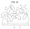
なお、本発明は、上記実施例に限定されるものではなく、発明の趣旨を逸脱しない範囲で種々の変形又は変更が可能である。例えば、本発明に係る光検出器は、図16に概略斜視図を示すように、金属層30を含む凹凸構造の複数の柱状の凸部が、任意の曲率又は角度で湾曲又は屈曲されて、任意の形状に形成されていてもかまわない。この場合、金属層30を含む凹凸構造の凸部の高さh、つまり金属層30の凸部と凹部との垂直方向の幅は、上述した本発明に係る光検出器の場合と同様に、検出光の波長以下の寸法、より好ましくは検出波長の1/10~1/5で、かつ凸部の太さ、つまり凸部の高さ方向に垂直な断面における最大寸法dは検出光の波長以下とする。
10 光検出器
20 有機半導体
30 金属層
40 半導体
40a 接合部
50 電流検出部
60、61、62、63 光検出器
70 シリコン基板
70a 接合部
71 導電性基板
72 ポリイミド基板
73 透明電極
75 ガラス基板
80 有機半導体部
80a 接合部
90 Au層
100 Al層
110 金属接合部
20 有機半導体
30 金属層
40 半導体
40a 接合部
50 電流検出部
60、61、62、63 光検出器
70 シリコン基板
70a 接合部
71 導電性基板
72 ポリイミド基板
73 透明電極
75 ガラス基板
80 有機半導体部
80a 接合部
90 Au層
100 Al層
110 金属接合部
Claims (15)
- 凸部を有する有機半導体と、
前記有機半導体上に付加され、検出光の照射により電子が励起される局在プラズモン共鳴及び表面プラズモン共鳴の少なくとも一方のプラズモン共鳴を促進する金属層と、
前記金属層に接合され、前記プラズモン共鳴により励起される電子を前記金属層との接合部において通過させる半導体と、
を備える光検出器。 - 請求項1に記載の光検出器において、
前記金属層を含む凸部の高さは、前記検出光の波長以下の寸法で、該凸部の太さの最大寸法が前記検出光の波長以下の寸法である、ことを特徴とする光検出器。 - 請求項1又は2に記載の光検出器において、
前記半導体は有機半導体である、ことを特徴とする光検出器。 - 請求項1~3のいずれか一項に記載の光検出器において、
前記半導体を支持する基板をさらに備える、ことを特徴とする光検出器。 - 請求項4に記載の光検出器において、
前記基板は半導体基板である、ことを特徴とする光検出器。 - 請求項4に記載の光検出器において、
前記基板は導電性基板である、ことを特徴とする光検出器。 - 請求項4に記載の光検出器において、
前記基板は絶縁性基板である、ことを特徴とする光検出器。 - 請求項1又は2に記載の光検出器において、
前記半導体は無機半導体である、ことを特徴とする光検出器 - 請求項1~8のいずれか一項に記載の光検出器において、
前記金属層を含む凸部の高さが20nm以上である、ことを特徴とする光検出器。 - 請求項1~8のいずれか一項に記載の光検出器において、
前記金属層を含む凸部の高さが50nm以上である、ことを特徴とする光検出器。 - 請求項1~10のいずれか一項に記載の光検出器において、
前記金属層は、凸部と該凸部に隣接する凹部とを有する凹凸構造であって、
前記凹凸構造の凸部の高さは、前記検出光の波長以下の寸法で、かつ該凸部の太さの最大寸法が前記検出光の波長以下の寸法である、ことを特徴とする光検出器。 - 請求項1~11のいずれか一項に記載の光検出器において、
前記金属層を含む凸部は、任意の形状に湾曲又は屈曲して形成されている、ことを特徴とする光検出器。 - 請求項1~12のいずれか一項に記載の光検出器において、
前記有機半導体は、フタロシアニン系、チオフェン系、Alq3のいずれかからなる、ことを特徴とする光検出器。 - 請求項1~13のいずれか一項に記載の光検出器において、
前記金属層は、Au、Pt、Al、Agのいずれかからなる、ことを特徴とする光検出器。 - 請求項1~14のいずれか一項に記載の光検出器において、
前記半導体は、フタロシアニン系、チオフェン系、Alq3、シリコンのいずれかからなる、ことを特徴とする光検出器。
Priority Applications (1)
| Application Number | Priority Date | Filing Date | Title |
|---|---|---|---|
| US14/936,244 US10290823B2 (en) | 2013-05-23 | 2015-11-09 | Photodetector |
Applications Claiming Priority (2)
| Application Number | Priority Date | Filing Date | Title |
|---|---|---|---|
| JP2013109015A JP6245495B2 (ja) | 2013-05-23 | 2013-05-23 | 光検出器 |
| JP2013-109015 | 2013-05-23 |
Related Child Applications (1)
| Application Number | Title | Priority Date | Filing Date |
|---|---|---|---|
| US14/936,244 Continuation US10290823B2 (en) | 2013-05-23 | 2015-11-09 | Photodetector |
Publications (1)
| Publication Number | Publication Date |
|---|---|
| WO2014188784A1 true WO2014188784A1 (ja) | 2014-11-27 |
Family
ID=51933350
Family Applications (1)
| Application Number | Title | Priority Date | Filing Date |
|---|---|---|---|
| PCT/JP2014/059060 Ceased WO2014188784A1 (ja) | 2013-05-23 | 2014-03-20 | 光検出器 |
Country Status (3)
| Country | Link |
|---|---|
| US (1) | US10290823B2 (ja) |
| JP (1) | JP6245495B2 (ja) |
| WO (1) | WO2014188784A1 (ja) |
Families Citing this family (14)
| Publication number | Priority date | Publication date | Assignee | Title |
|---|---|---|---|---|
| US11231544B2 (en) | 2015-11-06 | 2022-01-25 | Magic Leap, Inc. | Metasurfaces for redirecting light and methods for fabricating |
| EP3452301B1 (en) * | 2016-05-06 | 2024-08-14 | Magic Leap, Inc. | Metasurfaces with asymemtric gratings for redirecting light and methods for fabricating |
| US11011716B2 (en) * | 2016-08-02 | 2021-05-18 | King Abdullah University Of Science And Technology | Photodetectors and photovoltaic devices |
| JP7142015B2 (ja) | 2017-01-27 | 2022-09-26 | マジック リープ, インコーポレイテッド | 異なって向けられたナノビームを有するメタ表面によって形成された回折格子 |
| JP6928931B2 (ja) * | 2017-05-08 | 2021-09-01 | 国立大学法人電気通信大学 | 計測用デバイス及び計測センサ |
| JP6918631B2 (ja) * | 2017-08-18 | 2021-08-11 | 浜松ホトニクス株式会社 | 光検出素子 |
| JP7084020B2 (ja) * | 2018-01-19 | 2022-06-14 | 国立大学法人電気通信大学 | 分光用デバイス、分光器、及び分光測定方法 |
| JP6979929B2 (ja) * | 2018-06-25 | 2021-12-15 | 浜松ホトニクス株式会社 | 光検出器 |
| CN109524486B (zh) * | 2018-09-28 | 2022-09-23 | 暨南大学 | 一种电读出光学传感器 |
| KR102749135B1 (ko) * | 2019-03-06 | 2025-01-03 | 삼성전자주식회사 | 이미지 센서 및 이미징 장치 |
| JP6980292B2 (ja) * | 2019-10-29 | 2021-12-15 | 國立台灣大學 | 光検出器 |
| JP7488761B2 (ja) * | 2020-12-25 | 2024-05-22 | 浜松ホトニクス株式会社 | 光検出器 |
| CN115810680B (zh) * | 2022-09-21 | 2023-09-26 | 广东工业大学 | 一种局域场增强的光电导型高速光电探测器 |
| CN117650190B (zh) * | 2023-12-19 | 2024-06-14 | 广东工业大学 | 一种适用于非偏振光的等离激元电极光电探测器 |
Citations (3)
| Publication number | Priority date | Publication date | Assignee | Title |
|---|---|---|---|---|
| JP2011108722A (ja) * | 2009-11-13 | 2011-06-02 | Konica Minolta Holdings Inc | 有機太陽電池素子及び有機太陽電池素子の製造方法 |
| US20120048368A1 (en) * | 2010-09-01 | 2012-03-01 | Iowa State University Research Foundation, Inc. | Textured Micrometer Scale Templates as Light Managing Fabrication Platform for Organic Solar Cells |
| JP2012233779A (ja) * | 2011-04-28 | 2012-11-29 | Univ Of Tokyo | Sprセンサとsprセンサを搭載する検査システム |
Family Cites Families (14)
| Publication number | Priority date | Publication date | Assignee | Title |
|---|---|---|---|---|
| US6946597B2 (en) * | 2002-06-22 | 2005-09-20 | Nanosular, Inc. | Photovoltaic devices fabricated by growth from porous template |
| JP4583025B2 (ja) * | 2003-12-18 | 2010-11-17 | Jx日鉱日石エネルギー株式会社 | ナノアレイ電極の製造方法およびそれを用いた光電変換素子 |
| US8310373B2 (en) * | 2005-10-19 | 2012-11-13 | Schweitzer Engineering Laboratories, Inc. | System, a tool and a method for communicating with a faulted circuit indicator using a display |
| US7635600B2 (en) * | 2005-11-16 | 2009-12-22 | Sharp Laboratories Of America, Inc. | Photovoltaic structure with a conductive nanowire array electrode |
| US7960717B2 (en) * | 2005-12-29 | 2011-06-14 | E.I. Du Pont De Nemours And Company | Electronic device and process for forming same |
| JP4772585B2 (ja) * | 2006-05-10 | 2011-09-14 | 浜松ホトニクス株式会社 | 光検出器 |
| US7955889B1 (en) * | 2006-07-11 | 2011-06-07 | The Trustees Of Princeton University | Organic photosensitive cells grown on rough electrode with nano-scale morphology control |
| WO2008108406A1 (ja) * | 2007-03-05 | 2008-09-12 | Fujifilm Corporation | フォトレジスト用化合物、フォトレジスト液、およびこれを用いるエッチング方法 |
| EP2171735A1 (en) * | 2007-07-25 | 2010-04-07 | Polymers CRC Limited | Solar cell and method for preparation thereof |
| US20110039459A1 (en) * | 2009-08-11 | 2011-02-17 | Yancey Jerry W | Solderless carbon nanotube and nanowire electrical contacts and methods of use thereof |
| US9372283B2 (en) * | 2009-11-13 | 2016-06-21 | Babak NIKOOBAKHT | Nanoengineered devices based on electro-optical modulation of the electrical and optical properties of plasmonic nanoparticles |
| US8859423B2 (en) * | 2010-08-11 | 2014-10-14 | The Arizona Board Of Regents On Behalf Of The University Of Arizona | Nanostructured electrodes and active polymer layers |
| WO2014178923A2 (en) * | 2013-01-25 | 2014-11-06 | University Of Florida Research Foundation, Inc. | A novel ir image sensor using a solution processed pbs photodetector |
| US9331293B2 (en) * | 2013-03-14 | 2016-05-03 | Nutech Ventures | Floating-gate transistor photodetector with light absorbing layer |
-
2013
- 2013-05-23 JP JP2013109015A patent/JP6245495B2/ja not_active Expired - Fee Related
-
2014
- 2014-03-20 WO PCT/JP2014/059060 patent/WO2014188784A1/ja not_active Ceased
-
2015
- 2015-11-09 US US14/936,244 patent/US10290823B2/en active Active
Patent Citations (3)
| Publication number | Priority date | Publication date | Assignee | Title |
|---|---|---|---|---|
| JP2011108722A (ja) * | 2009-11-13 | 2011-06-02 | Konica Minolta Holdings Inc | 有機太陽電池素子及び有機太陽電池素子の製造方法 |
| US20120048368A1 (en) * | 2010-09-01 | 2012-03-01 | Iowa State University Research Foundation, Inc. | Textured Micrometer Scale Templates as Light Managing Fabrication Platform for Organic Solar Cells |
| JP2012233779A (ja) * | 2011-04-28 | 2012-11-29 | Univ Of Tokyo | Sprセンサとsprセンサを搭載する検査システム |
Non-Patent Citations (5)
| Title |
|---|
| E.ALTIN: "Dark current and optical properties in asymmetric GaAs/AlGaAs staircase-like multiquantum well structure", INFRARED PHYSICS & TECHNOLOGY, vol. 58, May 2013 (2013-05-01), pages 74 - 79 * |
| J.J.MOCK: "Shape effects in plasmon resonance of individual colloidal silver nanoparticles", THE JOURNAL OF CHEMICAL PHYSICS, vol. 116, no. 15, 2002, pages 6755 - 6759, XP008058604, DOI: doi:10.1063/1.1462610 * |
| KEIZO KATO: "Surface Plasmon Excitations and Emission Lights in Nanostructured Organic Dye Films", IEICE TECHNICAL REPORT, OME2010-61, 2011, pages 1 - 6 * |
| M . CASALINO: "A silicon compatible resonant cavity enhanced photodetector working at 1.55 pm", SEMICONDUCTOR SCIENCE AND TECHNOLOGY, vol. 23, no. 7, 2008, pages 1 - 7, XP020134796 * |
| YANXIA CUI: "Ultrabroadband Light Absorption by a Sawtooth Anisotropic Metamaterial Slab", NANO LETTERS, vol. 12, no. 3, 2012, pages 1443 - 1447 * |
Also Published As
| Publication number | Publication date |
|---|---|
| US20160064679A1 (en) | 2016-03-03 |
| JP6245495B2 (ja) | 2017-12-13 |
| JP2014229779A (ja) | 2014-12-08 |
| US10290823B2 (en) | 2019-05-14 |
Similar Documents
| Publication | Publication Date | Title |
|---|---|---|
| JP6245495B2 (ja) | 光検出器 | |
| Zhu et al. | Engineering plasmonic hot carrier dynamics toward efficient photodetection | |
| Qi et al. | Au nanoparticle-decorated silicon pyramids for plasmon-enhanced hot electron near-infrared photodetection | |
| Li et al. | Controllable vapor-phase growth of inorganic perovskite microwire networks for high-efficiency and temperature-stable photodetectors | |
| Garnett et al. | Light trapping in silicon nanowire solar cells | |
| Knight et al. | Embedding plasmonic nanostructure diodes enhances hot electron emission | |
| Liang et al. | Near‐infrared‐light photodetectors based on one‐dimensional inorganic semiconductor nanostructures | |
| Afshinmanesh et al. | Transparent metallic fractal electrodes for semiconductor devices | |
| Lu et al. | A localized surface plasmon resonance and light confinement‐enhanced near‐infrared light photodetector | |
| US20140175546A1 (en) | Plasmonically enhanced electro-optic devices and methods of production | |
| Ajiki et al. | Silicon based near infrared photodetector using self-assembled organic crystalline nano-pillars | |
| US20180102491A1 (en) | Organic photodetectors and production method thereof | |
| Wu et al. | Non‐ultrawide bandgap semiconductor GaSe nanobelts for sensitive deep ultraviolet light photodetector application | |
| US9252303B2 (en) | Thin film photovoltaic cell structure, nanoantenna, and method for manufacturing | |
| Feng Lu et al. | Plasmonic quantum dot solar cells for enhanced infrared response | |
| US10784393B2 (en) | Photodetection element having a periodic nano-concave/convex structure | |
| Wang et al. | Hybrid Si nanocones/PEDOT: PSS solar cell | |
| Kumawat et al. | Indium‐rich InGaN/GaN solar cells with improved performance due to plasmonic and dielectric nanogratings | |
| US9240511B2 (en) | Photodetector using surface plasmon resonance and image sensor having the same | |
| Park et al. | Plasmonic nanoparticles on graphene absorber for broadband high responsivity 2D/3D photodiode | |
| Lee et al. | Tandem-structured, hot electron based photovoltaic cell with double Schottky barriers | |
| Lin et al. | Packaging glass with a hierarchically nanostructured surface: A universal method to achieve self-cleaning omnidirectional solar cells | |
| Wang et al. | Back-reflected performance-enhanced flexible perovskite photodetectors through substrate texturing with femtosecond laser | |
| US11004999B2 (en) | Photodetector element | |
| KR101580740B1 (ko) | 그래핀/다공성 실리콘 융복합 나노 구조체를 이용한 포토 다이오드 및 그 제조방법 |
Legal Events
| Date | Code | Title | Description |
|---|---|---|---|
| 121 | Ep: the epo has been informed by wipo that ep was designated in this application |
Ref document number: 14801296 Country of ref document: EP Kind code of ref document: A1 |
|
| NENP | Non-entry into the national phase |
Ref country code: DE |
|
| 122 | Ep: pct application non-entry in european phase |
Ref document number: 14801296 Country of ref document: EP Kind code of ref document: A1 |