WO2014174997A1 - カンチレバー、製造方法、検査装置及び検査方法 - Google Patents
カンチレバー、製造方法、検査装置及び検査方法 Download PDFInfo
- Publication number
- WO2014174997A1 WO2014174997A1 PCT/JP2014/059361 JP2014059361W WO2014174997A1 WO 2014174997 A1 WO2014174997 A1 WO 2014174997A1 JP 2014059361 W JP2014059361 W JP 2014059361W WO 2014174997 A1 WO2014174997 A1 WO 2014174997A1
- Authority
- WO
- WIPO (PCT)
- Prior art keywords
- cantilever
- sample
- ray
- unit
- inspection apparatus
- Prior art date
- Legal status (The legal status is an assumption and is not a legal conclusion. Google has not performed a legal analysis and makes no representation as to the accuracy of the status listed.)
- Ceased
Links
Images







Classifications
-
- G—PHYSICS
- G21—NUCLEAR PHYSICS; NUCLEAR ENGINEERING
- G21K—HANDLING OF PARTICLES OR IONISING RADIATION NOT OTHERWISE PROVIDED FOR; IRRADIATION DEVICES; GAMMA RAY OR X-RAY MICROSCOPES
- G21K7/00—Gamma- or X-ray microscopes
-
- G—PHYSICS
- G01—MEASURING; TESTING
- G01Q—SCANNING-PROBE TECHNIQUES OR APPARATUS; APPLICATIONS OF SCANNING-PROBE TECHNIQUES, e.g. SCANNING PROBE MICROSCOPY [SPM]
- G01Q30/00—Auxiliary means serving to assist or improve the scanning probe techniques or apparatus, e.g. display or data processing devices
- G01Q30/02—Non-SPM analysing devices, e.g. SEM [Scanning Electron Microscope], spectrometer or optical microscope
-
- G—PHYSICS
- G01—MEASURING; TESTING
- G01Q—SCANNING-PROBE TECHNIQUES OR APPARATUS; APPLICATIONS OF SCANNING-PROBE TECHNIQUES, e.g. SCANNING PROBE MICROSCOPY [SPM]
- G01Q60/00—Particular types of SPM [Scanning Probe Microscopy] or microscopes; Essential components thereof
- G01Q60/24—AFM [Atomic Force Microscopy] or apparatus therefor, e.g. AFM probes
- G01Q60/38—Probes, their manufacture, or their related instrumentation, e.g. holders
- G01Q60/40—Conductive probes
-
- G—PHYSICS
- G01—MEASURING; TESTING
- G01N—INVESTIGATING OR ANALYSING MATERIALS BY DETERMINING THEIR CHEMICAL OR PHYSICAL PROPERTIES
- G01N2223/00—Investigating materials by wave or particle radiation
- G01N2223/20—Sources of radiation
- G01N2223/204—Sources of radiation source created from radiated target
Definitions
- Various aspects and embodiments of the present invention relate to a cantilever, a manufacturing method, an inspection apparatus, and an inspection method.
- the X-ray generators are used in various fields such as X-ray non-destructive inspection.
- the X-ray generator includes an electron gun that emits an electron beam and an X-ray generation target that is irradiated with the electron beam emitted from the electron gun.
- the X-ray generator emits X-rays by colliding an electron beam emitted from an electron gun with an X-ray generation target.
- the magnification by the X-ray generator is improved by, for example, increasing the position for measuring the X-rays after being irradiated on the sample.
- the above-described conventional technique has a problem that the magnification by the X-ray generator cannot be easily enlarged. For example, if the position for measuring the X-rays after being irradiated on the sample is to be increased, the structure of the apparatus becomes large.
- the disclosed cantilever is a cantilever in which an X-ray target portion is embedded in one embodiment.
- the distance between the sample and the X-ray target can be controlled with high accuracy.
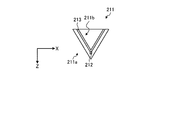
- FIG. 1 is an example of a cantilever according to the first embodiment.
- FIG. 2 is a view of the cantilever according to the first embodiment viewed from the probe side.
- FIG. 3 is a view of the cantilever according to the first embodiment, as viewed from above, where the probe is provided.
- FIG. 4 shows an example of a cross-sectional view of the probe in the XZ plane of the cantilever according to the first embodiment.
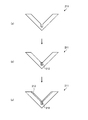
- FIG. 5 is a flowchart for explaining an example of the method for manufacturing the target for X-ray generation according to the first embodiment.
- FIG. 6 is a diagram for explaining an example of a method for manufacturing an X-ray generation target according to the first embodiment.
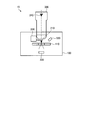
- FIG. 7 is a diagram illustrating an example of the configuration of the inspection apparatus according to the first embodiment.
- FIG. 8 is a flowchart illustrating an example of a processing flow in the first embodiment.
- FIG. 9 is a flowchart for explaining an example of the control method of the inspection apparatus according to the second embodiment.
- FIG. 10 is a diagram illustrating an example of the X-ray target unit in the second embodiment.
- FIG. 11 is a diagram illustrating an example of a conductive layer according to the second embodiment.
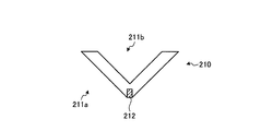
- FIG. 12 is a diagram showing an example of a cantilever used as an X-ray scanning probe.
- the cantilever according to the first embodiment is embedded with an X-ray target portion in an example of the embodiment.
- the X-ray target portion is embedded in the probe of the cantilever.
- the cantilever in the first embodiment is formed of a material containing an element whose cantilever probe is lighter than Si.
- the step of forming a bottomed hole in the cantilever and the X-ray target portion is formed by depositing metal in the hole provided in the cantilever. Including the step of.
- the inspection apparatus includes a vacuum chamber in which a sample stage on which a sample is placed is provided in an example of the embodiment.
- the inspection apparatus according to the first embodiment includes a cantilever provided in a vacuum chamber in an example of the embodiment, and atoms that acquire information on the surface of the sample placed on the sample table using the cantilever. It has an atomic force microscope.
- the inspection apparatus in 1st Embodiment has an X-ray inspection apparatus part provided with the electron gun which discharge
- the cantilever of the atomic force microscope unit is embedded with an X-ray target unit.
- an electron beam from an electron gun is used. Is irradiated to the X-ray target portion embedded in the cantilever, the sample is irradiated with X-rays, and the X-ray detection unit detects the X-rays after passing through the sample.
- the inspection apparatus includes a chamber in which a sample stage on which a sample is placed is provided, a first inspection unit that acquires sample information using a cantilever, and X-ray information about the sample. And a second inspection unit to be obtained by using. Further, the cantilever inspects, for example, unevenness on the sample surface or an electric signal.
- the inspection method according to the first embodiment includes a vacuum chamber in which a sample stage on which a sample is placed is provided, and a cantilever provided in the vacuum chamber.
- An atomic force microscope unit that acquires information on the surface of the sample that has been obtained using a cantilever, and an X-ray inspection apparatus unit that includes an electron gun that emits an electron beam, an X-ray target unit, and an X-ray detection unit This is a method for controlling an inspection apparatus.
- the atomic force microscope unit acquires information on the surface of the sample placed on the sample stage using a cantilever.
- the X-ray inspection apparatus emits an electron beam from the electron gun in a state where the information on the surface of the sample is acquired after the information on the surface of the sample is acquired using the cantilever by the atomic force microscope unit.
- the X-ray detector detects X-rays from the sample placed on the sample table.
- FIG. 1 is a diagram illustrating an example of a cantilever according to the first embodiment.
- FIG. 1 is a view of the cantilever according to the first embodiment viewed in the Y-axis direction.
- FIG. 2 is a view of the cantilever according to the first embodiment viewed from the probe side.
- the cantilever 210 is embedded with an X-ray target portion 212.
- the X-ray target unit 212 is embedded in the probe 211 of the cantilever 210.
- a portion corresponding to a portion where the X-ray target unit 212 is embedded is indicated by a dotted line.
- FIG. 3 is a view of the cantilever according to the first embodiment, as viewed from above, where the probe is provided.
- FIG. 3 shows an example of a location where the probe of the cantilever according to the first embodiment is provided when viewed in the Z-axis direction.
- FIG. 4 is a diagram illustrating an example of a cross-sectional configuration of a portion where the probe is provided in the cantilever according to the first embodiment.
- FIG. 4 shows an example of a cross-sectional view of the XZ plane of the probe in the cantilever according to the first embodiment.
- FIG. 4 shows an example of a cross-sectional view of the XZ plane of the probe in the cantilever according to the first embodiment.
- the cantilever 210 when viewed in the Z-axis direction, has a concave portion whose shape is a quadrangular pyramid with the location where the X-ray target portion 212 is provided at the location where the probe 211 is provided.
- the present invention is not limited to this, and the concave portion may not be provided, and the shape of the convex portion may be arbitrary.
- the concave portion it is possible to facilitate positioning when emitting an electron beam to the cantilever 210 by forming a shape having a vertex where the X-ray target portion 212 is provided.
- the probe 211 has a first surface 211a facing the sample stage 110 side of an inspection apparatus using a cantilever 210 described later, and an electron that emits an electron beam of the inspection apparatus described later. And a second surface 211b facing the gun 310 side.
- the probe 211 has a bottomed hole at the tip thereof on the second surface 211 b side, and an X-ray target portion at the bottomed hole at the tip. 212 is embedded.
- the shape of the bottomed hole provided in the probe 211 may be an arbitrary shape such as a cylindrical shape or a prismatic shape.
- the diameter of the bottomed hole is set to, for example, about 100 nm, and the depth is set to, for example, about 1 ⁇ m.
- the bottomed hole provided in the probe 211 is formed with a small diameter and a large aspect ratio of the hole.
- the conductive layer 213 is provided in a portion other than the irradiation line irradiated with X-rays from the X-ray target unit 212. In other words, it is provided on a part or all of the portion excluding the line connecting the X-ray target unit 212 and a sample placed on the sample stage 110 described later.
- the probe 211 has a conductive layer 213 provided on the second surface 211b.
- the conductive layer 213 is formed on the second surface 211b using a conductor such as titanium, chromium, or a surface layer having an ion dove layer formed thereon, for example.
- the thickness of the conductive layer 213 is, for example, about 50 nm, but is not limited to this, and may be an arbitrary value. Further, the conductive layer 213 is not necessarily provided when the cantilever 210 is formed of a conductive material.
- the probe 211 of the cantilever 210 is preferably a light element that has high thermal diffusibility and does not absorb X-rays, and preferably has a higher heat dissipation.
- a material with high heat dissipation it is possible to efficiently diffuse the heat generated when generating X-rays, and a large current can be applied.
- X-rays generated in the X-ray target unit 212 can be efficiently emitted toward the stage.
- the cantilever probe 211 is formed of a material containing an element lighter than Si, for example.
- Materials for forming the cantilever probe 211 are diamond, diamond-like carbon doped with impurities (for example, boron), ceramic (for example, boron nitride, silicon nitride). , Aluminum nitride, alumina, silicon oxide).
- the material forming the cantilever probe 211 is more preferably diamond. Note that portions other than the probe 211 in the cantilever 210 may be formed using the same material as the probe 211 or may be formed using a different material.
- the X-ray target unit 212 is formed in a bottomed hole formed at the tip of the probe 211, for example.
- the metal that forms the X-ray target portion 212 is, for example, copper, molybdenum, tungsten, gold, platinum, or the like.
- the X-ray target unit 212 is formed by depositing metal in a bottomed hole formed in the probe 211, for example. As a result, the entire X-ray target portion 212 is in close contact with the bottom surface and the side wall surface of the hole.
- the X-ray target portion 212 is formed corresponding to the shape of the inner space of the bottomed hole formed in the probe 211.
- the length of the columnar axial direction of the X-ray target portion 212 is, for example, about 1 ⁇ m.
- the length of the cylindrical shape of the X-ray target 212 in the radial direction is, for example, about 100 nm.
- FIG. 5 is a flowchart for explaining an example of the method for manufacturing the target for X-ray generation according to the first embodiment.
- FIG. 6 is a diagram for explaining an example of a method for manufacturing an X-ray generation target according to the first embodiment.
- FIB focused ion beam
- the cantilever 210 is placed on the mounting table of the FIB apparatus (step S101). At this time, only the probe 211 of the cantilever 210 may be arranged. Then, the FIB apparatus forms a bottomed hole in the cantilever (step S102). For example, the FIB apparatus forms a hole in the probe 211 of the cantilever 210. Specifically, the FIB apparatus forms a bottomed hole in the probe 211 of the cantilever 210.
- the FIB apparatus irradiates the tip of the probe 211 of the cantilever 210 with an ion beam such as Ga +, thereby sputtering from the second surface 211b side, and has a bottomed shape as shown in FIG. Form a hole.
- the FIB apparatus forms a hole having a diameter of 100 nm and a depth of 600 nm at the tip of the probe 211 of the cantilever 210.
- the present invention is not limited to this, and the hole diameter may be smaller than 100 nm and the depth may be deeper than 600 nm.
- the holes formed by sputtering the tip portion of the probe 211 of the cantilever 210 with an ion beam each have a diameter that decreases toward the bottom surface, and the side wall surface may be tapered.
- the case where the side wall surface is formed vertically from the bottom surface is shown as an example for convenience of description.
- the X-ray target unit 212 is formed (step S103). That is, as shown in FIG. 6B, the X-ray target portion 212 is formed by depositing metal in a hole provided in the cantilever 210. Here, metal is deposited directly in the hole. As a result, the X-ray target unit 212 and the side surface and bottom surface of the hole are in close contact with each other.
- the metal is deposited by irradiating the hole with a focused ion beam in a gas atmosphere containing metal atoms using an FIB processing apparatus.
- the material is deposited by FIB-excited chemical vapor deposition by spraying a material gas onto the irradiated portion of the focused ion beam.
- tungsten can be deposited by using tungsten hexacarbonyl (W (CO) 6) as a material gas.
- W (CO) 6 tungsten hexacarbonyl
- platinum can be deposited by using trimethyl (methylcyclopentadienyl) platinum as a material gas.
- gold can be deposited by using dimethyl gold hexafluoroacetylacetonate (C7H7F6O2Au) as a material gas.
- the conductive layer 213 is formed (step S104).
- the conductive layer 213 is formed on the second surface 211b of the probe 211 so as to cover the X-ray target portion 212 formed in the hole.
- the conductive layer 213 is formed using, for example, a known film forming apparatus.
- the conductive layer 213 is formed by generating and growing diamond particles while doping boron by a microwave plasma CVD method using a microwave plasma CVD apparatus.
- the conductive layer 213 is formed using, for example, a known PVD (Physical Vapor Deposition).
- the conductive layer 213 is formed by depositing a conductive metal film using a PVD apparatus.
- the conductive metal film is made of, for example, a metal such as titanium or chromium and has a thickness of 50 nm.
- the material for forming the conductive metal film is not limited to this, and a material other than titanium or chromium may be used.
- the film thickness is preferably 1/10 or less of the thickness (depth) of the X-ray target portion 212.
- the film thickness is 50 nm or thinner than 50 nm.
- a place where the film thickness is greater than 50 nm and a place where the film thickness is 50 nm and less than 50 nm may be provided.
- the film thickness may be changed according to the film material and the energy of X-rays to be generated. As a result, a conductive layer 213 is formed on the second surface 211b of the probe 211 as shown in FIG.
- step S104 described above may be omitted, and step S104 may be performed before step S102.
- the inspection apparatus in the first embodiment has a vacuum chamber in which a sample stage on which a sample is placed is provided.
- the inspection apparatus according to the first embodiment includes a cantilever provided in a vacuum chamber, and includes an atomic force microscope unit that acquires information on the surface of the sample placed on the sample stage using the cantilever.
- the inspection apparatus according to the first embodiment includes an X-ray inspection apparatus unit including an electron gun that emits an electron beam, an X-ray target unit, and an X-ray detection unit.
- the X-ray target part is embedded in the cantilever of the atomic force microscope part.
- the X-ray inspection apparatus unit irradiates the sample with X-rays emitted by irradiating the X-ray target unit embedded in the cantilever with an electron beam from the electron gun.
- the X-ray detection unit detects X-rays after passing through the sample.
- FIG. 7 is a diagram illustrating an example of the configuration of the inspection apparatus according to the first embodiment.
- the inspection apparatus 10 includes a vacuum chamber 100, an atomic force microscope unit (AFM, Atomic Force Microscope) 200, and an X-ray inspection apparatus unit 300.
- the X-ray inspection apparatus unit 300 may be provided with a function of a scanning electron microscope (SEM, Scanning Electron Microscope).
- a sample stage 110 on which a sample to be measured by the X-ray inspection apparatus unit 300 is placed is provided inside the vacuum chamber 100, and a cantilever is placed inside the vacuum chamber 100.
- An atomic force microscope unit 200 having 210 is provided.
- the atomic force microscope unit 200 and the X-ray inspection apparatus unit 300 will be described, respectively, but the points similar to those of the known atomic force microscope and scanning electron microscope will be omitted as appropriate, Or make the description concise.
- the sample stage 110 is provided inside the vacuum chamber 100, and a sample to be measured by the X-ray inspection apparatus unit 300 and the atomic force microscope unit 200 is placed thereon.
- a sample to be measured by the X-ray inspection apparatus unit 300 and the atomic force microscope unit 200 is placed thereon.
- an AFM module that can be operated in a compact manner or a compact optical lever scanning module.
- the sample stage 110 is a transmissive stage formed of a material that transmits X-rays, or passes X-rays generated from the X-ray target unit 212 and detected by an X-ray detection unit 330 described later. Has a hole.
- a piezo stage capable of XY ⁇ drive.
- the X-ray detection unit 330 is, for example, an X-ray image intensifier (X-ray I.I.) or an X-ray CCD (Charge Coupled Device) camera.
- X-ray I.I. X-ray image intensifier
- CCD Charge Coupled Device
- An X-ray camera using CsI (cesium iodide) and a CCD, a CMOS (Complementary Metal Oxide Semiconductor) camera, a flat panel for detecting X-rays, and the like are preferable.
- the atomic force microscope unit 200 includes a cantilever 210 provided in the vacuum chamber 100 and acquires information on the surface of the sample placed on the sample stage 110 using the cantilever 210.
- a known atomic force microscope may be used except that the cantilever 210 in the first embodiment is used.
- the atomic force acting between the probe 211 of the cantilever 210 and the sample placed on the sample stage 110 is detected as the deflection of the cantilever 210.
- the atomic force microscope unit 200 acquires the three-dimensional shape of the sample by scanning the sample in a horizontal plane while controlling the distance between the probe 211 and the sample so that the deflection of the cantilever 210 is constant. To do.
- the X-ray inspection apparatus unit 300 includes an electron gun 310 that emits an electron beam, an X-ray target unit 212, and an X-ray detection unit 330. By irradiating the X-ray target unit 212 with an electron beam from the electron gun 310, X-rays are emitted, and the X-ray detector 330 detects X-rays from the sample placed on the sample stage 110. In the example illustrated in FIG. 7, the X-ray inspection apparatus unit 300 further includes a detector 320 that detects secondary electrons generated from the sample or the X-ray target unit by irradiation with an electron beam.
- the electron gun 310 uses, for example, a TFE (Thermal Field Emission) having the same electron energy as an electron source.
- TFE Thermal Field Emission
- the adoption of TFE makes it easy to reduce the electron beam diameter.
- an electron beam is emitted from the electron gun 310, the electron beam is finely focused by a focus lens (not shown in FIG. 7), and focused on the surface of the sample by the objective lens.
- the top is scanned with an electron beam.
- the X-ray detection unit 330 detects secondary electrons generated from the sample or the X-ray target unit by being irradiated with the electron beam. Thereafter, the secondary electrons detected by the X-ray detection unit 330 are signal-processed to obtain an electron beam image.
- the electron beam image of the sample is acquired by scanning with the electron beam in a state where the cantilever 210 is not on the sample.
- the position of the X-ray target unit 212 provided on the cantilever 210 is identified by scanning with an electron beam while the cantilever 210 is on the sample.
- the X-ray inspection apparatus unit 300 irradiates the sample with X-rays emitted by irradiating the X-ray target unit 212 embedded in the cantilever 210 with an electron beam from the electron gun 310, and the X-ray detection unit 330. Detects X-rays after passing through the sample. In other words, the X-ray inspection apparatus unit 300 uses the X-rays emitted from the X-ray target unit 212 provided on the cantilever 210 to acquire an X-ray image of the sample at the portion where the probe 211 of the cantilever 210 is located. To do.
- the X-ray inspection apparatus unit 300 includes an X-ray detection unit 330 that detects X-rays in addition to a known scanning electron microscope.
- the X-ray inspection apparatus unit 300 shown in FIG. 7 irradiates the X-ray target unit 212 embedded in the cantilever 210 of the atomic force microscope unit 200 with an electron beam, so that the probe 211 of the cantilever 210 is moved.
- An X-ray image of the sample in the position is acquired. That is, for example, a sample pattern is measured from a concavo-convex image obtained by scanning the probe 211 on the surface of the sample.
- the cantilever 210 is stopped at the point to be observed, and the X-ray inspection apparatus unit 300 irradiates the X-ray target unit 212 with an electron beam and images with the lower X-ray camera through the sample stage 110 serving as a transmission stage. .
- the X-ray inspection apparatus unit 300 irradiates the X-ray target unit 212 with an electron beam and images with the lower X-ray camera through the sample stage 110 serving as a transmission stage.
- the information on the surface of the sample placed on the sample stage 110 having the vacuum chamber 100 on which the sample stage 110 on which the sample is placed and the cantilever 210 provided in the vacuum chamber 100 is provided. It has an atomic force microscope unit 200 acquired using a cantilever 210, an electron gun that emits an electron beam, and an X-ray detection unit. The electron gun emits an X-ray by irradiating the X-ray target unit with the electron beam.
- FIG. 8 is a flowchart for explaining an example of the control method of the inspection apparatus according to the first embodiment.
- the atomic force microscope unit 200 acquires information on the surface of the sample placed on the sample stage 110 using the cantilever 210 (Step S202).
- the atomic force microscope unit 200 detects the atomic force acting between the probe 211 of the cantilever 210 and the sample placed on the sample stage 110 as the deflection of the cantilever 210 at the position to be measured.
- the X-ray inspection apparatus unit 300 obtains the electron from the electron gun 310 in a state where the information on the surface of the sample is acquired after the information on the surface of the sample is acquired by the atomic force microscope unit 200 using the cantilever 210.
- the X-ray detector 330 detects X-rays from the sample placed on the sample stage 110 by irradiation with the beam (step S203). For example, in the inspection apparatus 10, when information on the surface of the sample is acquired by the atomic force microscope unit 200 using the cantilever 210, measurement by the atomic force microscope unit 200 is interrupted and the position of the cantilever 210 is not moved.
- the X-ray inspection apparatus unit 300 irradiates the X-ray target unit 212 embedded in the cantilever 210 with an electron beam, thereby acquiring an X-ray image of the sample in the portion where the probe 211 of the cantilever 210 is located. That is, an X-ray image at a position where the surface state is measured by the atomic force microscope unit 200 is acquired.
- the above processing procedures are not limited to the above order, and may be appropriately changed within a range in which the processing contents do not contradict each other.
- the measurement by the atomic force microscope unit 200 is interrupted, and the cantilever 210 is received. You may acquire the X-ray image in the position, without moving.
- the X-ray target unit 212 is embedded in the cantilever 210. As a result, the distance between the sample and the X-ray generation source can be reduced.
- the X-ray magnification is determined by the geometric position of the X-ray source, the sample, and the X-ray camera.
- the positions of the X-ray source and the sample cannot be reduced, high magnification cannot be obtained unless the camera is moved far away.
- the distance between the sample and the X-ray generation source can be reduced. As a result, it is possible to obtain a high magnification without increasing the position of the X-ray camera.
- the X-ray magnification can be improved and the inspection apparatus 10 can be downsized.
- the X-ray target unit 212 is embedded in the probe 211 of the cantilever 210.
- the distance between the sample and the X-ray generation source can be reduced.
- an X-ray image at a measurement location by the cantilever 210 can be easily and accurately acquired.
- the probe 211 of the cantilever 210 is formed of a material containing an element lighter than Si. As a result, it is possible to suppress the rate at which X-rays generated from the X-ray target unit 212 are absorbed by the cantilever 210, and the sample can be efficiently irradiated with X-rays.
- the X-ray target portion 212 can be reliably formed on the cantilever 210.
- the inspection apparatus 10 includes the vacuum chamber 100.
- the inspection apparatus 10 includes a cantilever 210 provided in the vacuum chamber 100 and includes an atomic force microscope unit 200 that acquires information on the surface of the sample placed on the sample stage 110 using the cantilever 210.
- the inspection apparatus 10 includes an electron gun 310 that emits an electron beam, an X-ray target unit, and an X-ray detection unit 330, and emits X-rays emitted by irradiating the electron beam from the electron gun 310.
- the X-ray inspection apparatus unit 300 is used by which the X-ray detection unit 330 detects X-rays from the sample placed on the sample stage 110.
- the X-ray target unit 212 is embedded in the cantilever 210 of the atomic force microscope unit 200, and the X-ray inspection apparatus unit 300 cantilever the electron beam from the electron gun 310.
- the sample is irradiated with X-rays by irradiating the X-ray target unit 212 embedded in 210, and the X-ray detection unit 330 detects the X-rays that have passed through the sample.
- an X-ray image is acquired after the cantilever 210 in which the X-ray target unit 212 is embedded is brought into contact with or in proximity to the sample, so that an enlargement magnification of tens of thousands of times can be realized in a compact configuration.
- the distance between the cantilever 210 and the sample is controlled to a fixed distance.
- the distance between the X-ray target unit 212 and the sample is always constant, and the distance between the surface structure and the X-ray source can be defined while tracing the surface of the sample. Therefore, the enlargement magnification can be determined with high accuracy.
- the atomic force microscope unit 200 acquires information on the surface of the sample placed on the sample stage 110 using the cantilever 210, and the X-ray inspection apparatus unit 300 uses the atomic force microscope 200. After the information on the surface of the sample is acquired by the atomic force microscope unit 200 using the cantilever 210, the X-ray target unit is irradiated with an electron beam while the information on the surface of the sample is acquired.
- the X-ray detector 330 detects X-rays from the sample placed on the sample stage 110 by emitting the rays. As a result, it is possible to easily and accurately perform observation of a three-dimensional microstructure and characteristic observation by AFM at the same position.
- Control method For example, in the example illustrated in FIG. 8, the case where the processing by the X-ray inspection apparatus unit 300 is performed after the measurement by the atomic force microscope unit 200 is described as an example, but the present invention is not limited thereto. .
- FIG. 9 after the process by the X-ray inspection apparatus unit 300 is performed, the measurement by the atomic force microscope unit 200 may be performed.
- FIG. 9 is a flowchart for explaining an example of the control method of the inspection apparatus according to the second embodiment.
- the X-ray inspection apparatus unit 300 emits an X-ray by emitting an electron beam from the electron gun 310 to the X-ray target unit, and is placed on the sample stage 110.
- the X-ray detector 330 detects X-rays from the placed sample (step S302).
- the atomic force microscope unit 200 uses the cantilever 210 to display information on the surface of the sample placed on the sample table 110 in a state where the X-ray is detected after the X-ray inspection apparatus unit 300 detects the X-ray. (Step S303).
- the atomic force microscope unit 200 acquires the X-ray image without moving the position of the cantilever 210.
- Information on the surface of the sample at the determined position is acquired using the cantilever 210.
- the present invention is not limited to this, and only the cantilever 210 is a vacuum chamber. The other portion may be provided outside the vacuum chamber 100. Moreover, the vacuum chamber 100 should just be pressure-reduced rather than atmospheric pressure. Moreover, you may use by atmospheric pressure according to a test object.
- the X-ray target unit 212 is provided as the cantilever 210 of the atomic force microscope unit 200 as an example, but the present invention is not limited to this.
- the X-ray target unit may be embedded in an arbitrary probe.
- an electronic circuit such as an LSI or a printed board may be embedded in a probe for electrical inspection.
- the cantilever may be a contact type or a non-contact type.
- the present invention is not limited to a cantilever for an atomic force microscope, and can be used for a cantilever of a scanning probe microscope such as a scanning tunneling microscope.
- the “cantilever” in the scope of the claims includes a probe. A plurality of cantilevers may be provided. Further, the atomic force microscope unit 200 and the X-ray inspection apparatus unit 300 may be calibrated using the mutual detection results.
- the X-ray image is not limited to the case of acquiring a planar image, and three-dimensional information may be acquired by moving the sample stage.
- a CT (Computed Tomography) image may be acquired.
- the X-ray target unit 212 is not limited to the case where the X-ray target unit 212 is embedded at the tip of the cantilever 210 from the second surface 211b, and may be embedded at an arbitrary location.
- FIG. 10 is a diagram illustrating an example of the X-ray target unit in the second embodiment. As shown in FIG. 10, the X-ray target unit 212 may be embedded from the first surface 211 a at the tip of the cantilever 210. Further, the X-ray target unit 212 may be embedded in the cantilever 210 at an arbitrary place instead of the tip. Further, the X-ray target unit 212 may be provided through the cantilever 210. Further, it may be formed on the surface of the cantilever 210.
- the conductive layer 213 is not limited to the case where the conductive layer 213 is provided on the second surface 211 b of the cantilever 210, and may be provided at an arbitrary place.
- FIG. 11 is a diagram illustrating an example of a conductive layer according to the second embodiment. In the example illustrated in FIG. 11, the conductive layer 213 is provided on the first surface 211a. However, in this case, preferably, the cantilever 210 has the conductive layer 213 in a portion other than the irradiation line 215 irradiated with the X-rays from the X-ray target unit 212. By providing the conductive layer 213 in this way, it is possible to prevent the conductive layer 213 from damaging the X-rays irradiated from the X-ray target unit 212 to the sample.
- FIG. 12 is a diagram showing an example of a cantilever 230 used as an X-ray scanning probe. As shown in FIG. 12, a hole stop 231 made of a metal capable of shielding X-rays may be provided at a position where the material at the probe tip of the cantilever 230 is sandwiched.
- X-rays are irradiated onto the hole-shaped stop 231 while synchronizing with the scanning by the cantilever 230, and the X-ray detection unit provided at the lower part of the sample passes through the sample after being stopped by the hole-shaped stop 231.
- Detect lines are constructed by constructing a scan image similar to the AFM using X-rays detected through the aperture stop 231 as a signal, an X-ray scan image by the X-ray probe can be acquired.
- the intensity of all X-rays transmitted through the aperture stop 231 is used as a signal of one pixel.
- the signal of one pixel corresponding to the position A is formed using the intensity of all the X-rays transmitted through the aperture stop 231 at the position A. Then, an X-ray scanning image is formed by forming a signal for the pixels corresponding to the other positions in synchronization with the cantilever. As a result, a highly sensitive image can be acquired. Further, by executing the processing while synchronizing with the scanning of the cantilever 230, it is possible to acquire an X-ray scanning image in addition to acquiring an AFM image. Further, by designing the diameter of the hole of the aperture stop 231 in accordance with the enlargement ratio, it is possible to acquire an X-ray scanning image having an arbitrary enlargement magnification.
- the X-ray target portion 212 provided in the cantilever 230 is not provided, and the X-ray irradiated to the hole-like diaphragm 231 is not provided in the hole shape provided in the cantilever 230.
- the case where the diaphragm 231 is irradiated with X-rays is shown as an example, but the present invention is not limited to this.
- the X-ray target unit 212 is further provided on the cantilever 230, the X-ray emitted from the X-ray target unit 212 is irradiated to the hole-shaped aperture 231, and the X-rays that have passed through the hole-shaped aperture 231 are applied to the sample.
Landscapes
- Physics & Mathematics (AREA)
- Health & Medical Sciences (AREA)
- General Health & Medical Sciences (AREA)
- General Physics & Mathematics (AREA)
- Nuclear Medicine, Radiotherapy & Molecular Imaging (AREA)
- Radiology & Medical Imaging (AREA)
- Engineering & Computer Science (AREA)
- General Engineering & Computer Science (AREA)
- High Energy & Nuclear Physics (AREA)
- Analysing Materials By The Use Of Radiation (AREA)
Abstract
開示のカンチレバー210は、実施形態の一例において、X線ターゲット部212が埋め込まれる。また、開示のカンチレバー210は、実施形態の一例において、X線ターゲット部212がカンチレバー210の探針211に埋め込まれる。また、開示のカンチレバーは、実施形態の一例において、カンチレバー210の探針211がSiより軽い元素を含む材料にて形成される。また、開示のカンチレバー210は、実施形態の一例において、X線ターゲット部212からX線が照射される照射線上を除く部分に導電層213を有する。
Description
本発明の種々の側面及び実施形態は、カンチレバー、製造方法、検査装置及び検査方法に関するものである。
X線発生装置は、X線非破壊検査など様々な分野で用いられている。X線発生装置は、電子ビームを放出する電子銃と、電子銃から放出された電子ビームが照射されるX線発生用ターゲットとを備える。X線発生装置は、電子銃から放出された電子ビームをX線発生用ターゲットに衝突させることで、X線を放出する。ここで、X線発生装置による拡大倍率は、例えば、試料に照射された後のX線を測定する位置を遠くにすることなどによって向上する。
しかしながら、上述した従来技術では、X線発生装置による拡大倍率を簡単に拡大できないという問題がある。例えば、試料に照射された後のX線を測定する位置を遠くにしようとすると、装置の構造が大きくなってしまう。
開示するカンチレバーは、1つの実施態様において、X線ターゲット部が埋め込まれたカンチレバーである。
開示するカンチレバーの1つの態様によれば、精度良くサンプルとX線ターゲット間の距離を制御できるという効果を奏する。
以下に、開示するカンチレバー、製造方法、検査装置及び検査方法の実施形態について、図面に基づいて詳細に説明する。なお、本実施形態により開示する発明が限定されるものではない。各実施形態は、処理内容を矛盾させない範囲で適宜組み合わせることが可能である。
(第1の実施形態)
第1の実施形態におけるカンチレバーは、実施形態の一例において、X線ターゲット部が埋め込まれる。また、例えば、第1の実施形態におけるカンチレバーは、X線ターゲット部がカンチレバーの探針に埋め込まれる。また、例えば、第1の実施形態におけるカンチレバーは、カンチレバーの探針がSiより軽い元素を含む材料にて形成される。
第1の実施形態におけるカンチレバーは、実施形態の一例において、X線ターゲット部が埋め込まれる。また、例えば、第1の実施形態におけるカンチレバーは、X線ターゲット部がカンチレバーの探針に埋め込まれる。また、例えば、第1の実施形態におけるカンチレバーは、カンチレバーの探針がSiより軽い元素を含む材料にて形成される。
また、第1の実施形態における製造方法は、実施形態の一例において、カンチレバーに有底状の穴を形成する工程と、カンチレバーに設けられた穴に金属を堆積させることでX線ターゲット部を形成する工程とを含む。
また、第1の実施形態における検査装置は、実施形態の一例において、試料が載置される試料台が設けられる真空チャンバを有する。また、第1の実施形態における検査装置は、実施形態の一例において、真空チャンバ内に設けられたカンチレバーを有し、試料台に載置された試料の表面の情報をカンチレバーを用いて取得する原子間力顕微鏡部を有する。また、第1の実施形態における検査装置は、実施形態の一例において、電子ビームを放出する電子銃と、X線ターゲット部と、X線検出部とを備えたX線検査装置部を有する。
また、第1の実施形態における検査装置は、実施形態の一例において、原子間力顕微鏡部のカンチレバーは、X線ターゲット部が埋め込まれており、X線検査装置部では、電子銃からの電子ビームをカンチレバーに埋め込まれたX線ターゲット部に照射することで放出されたX線を試料に照射し、X線検出部が、試料を透過した後のX線を検出する。
また、第1の実施形態における検査装置は、試料が載置される試料台が設けられるチャンバと、試料の情報をカンチレバーを用いて取得する第一の検査部と、試料の情報をX線を用いて取得する第二の検査部と、を有する。また、カンチレバーは、例えば、試料表面の凹凸または電気信号を検査する。
また、第1の実施形態における検査方法は、実施形態の一例において、試料が載置される試料台が設けられる真空チャンバと、真空チャンバ内に設けられたカンチレバーを有して試料台に載置された試料の表面の情報をカンチレバーを用いて取得する原子間力顕微鏡部と、電子ビームを放出する電子銃とX線ターゲット部とX線検出部とを備えたX線検査装置部とを有することを特徴とする検査装置の制御方法である。また、第1の実施形態における検査方法は、実施形態の一例において、原子間力顕微鏡部は、試料台に載置された試料の表面の情報をカンチレバーを用いて取得する。そして、X線検査装置部は、原子間力顕微鏡部によってカンチレバーを用いて試料の表面の情報が取得された後、試料の表面の情報が取得された状態において、電子銃から電子ビームを放出して試料台に載置された試料からのX線をX線検出部が検出する。
(第1の実施形態に係るカンチレバー)
図1及び図2を用いて、第1の実施形態に係るカンチレバーの全体像の一例について説明する。図1は、第1の実施形態に係るカンチレバーの一例を示す図である。言い換えると、図1は、第1の実施形態に係るカンチレバーをY軸方向に見た図である。図2は、第1の実施形態に係るカンチレバーを探針側から見た図である。図1及び図2に示すように、カンチレバー210は、X線ターゲット部212が埋め込まれる。図1に示す例では、X線ターゲット部212は、カンチレバー210の探針211に埋め込まれる。なお、図2では、X線ターゲット部212の埋め込まれている箇所に対応する箇所を点線で示した。
図1及び図2を用いて、第1の実施形態に係るカンチレバーの全体像の一例について説明する。図1は、第1の実施形態に係るカンチレバーの一例を示す図である。言い換えると、図1は、第1の実施形態に係るカンチレバーをY軸方向に見た図である。図2は、第1の実施形態に係るカンチレバーを探針側から見た図である。図1及び図2に示すように、カンチレバー210は、X線ターゲット部212が埋め込まれる。図1に示す例では、X線ターゲット部212は、カンチレバー210の探針211に埋め込まれる。なお、図2では、X線ターゲット部212の埋め込まれている箇所に対応する箇所を点線で示した。
図3は、第1の実施形態に係るカンチレバーのうち探針が設けられた箇所を上部から見た図である。言い換えると、図3は、Z軸方向に見た場合における第1の実施形態に係るカンチレバーの探針が設けられた箇所の一例を示す。図4は、第1の実施形態に係るカンチレバーのうち探針が設けられた箇所の断面構成の一例を示す図である。言い換えると、図4は、第1の実施形態に係るカンチレバーのうち探針のXZ平面の断面図の一例を示す。図3に示す例では、Z軸方向に見た場合に、カンチレバー210が、探針211が設けられた箇所に、X線ターゲット部212が設けられた箇所を頂点として形状が四角錐となる凹部を有する場合を例に示したが、これに限定されるものではなく、凹部を有さなくても良く、凸部の形状も任意であって良い。ただし、凹部を設ける場合、X線ターゲット部212が設けられた箇所を頂点とする形状とすることで、カンチレバー210に電子ビームを放出する際、位置決めを容易とすることが可能となる。
図3及び図4に示す例では、探針211は、後述するカンチレバー210が用いられる検査装置の試料台110側に面する第1の面211aと、後述する検査装置の電子ビームを放出する電子銃310側に面する第2の面211bとを有する。ここで、図3及び図4に示す例では、探針211は、先端部に有底状の穴が第2の面211b側に形成され、先端部の有底状の穴にX線ターゲット部212が埋め込まれる。
なお、探針211に設けられる有底状の穴の形状は、例えば、円柱体形状や角柱体形状など任意の形状であっても良い。また、有底状の穴の径は、例えば、100nm程度に設定され、深さが、例えば、1μm程度に設定される。このように、探針211に設けられる有底状の穴は、径が小さく形成されるとともに、穴のアスペクト比が大きく形成される。
また、導電層213は、X線ターゲット部212からX線が照射される照射線上を除く部分に設けられる。言い換えると、X線ターゲット部212と、後述の試料台110に置かれる試料とを結ぶ線上を除く部分の一部又は全てに設けられる。図1、図3及び図4に示す例では、探針211は、導電層213が第2の面211bに設けられる。
導電層213は、例えば、チタンやクロム、表層にイオンドーブ層を形成したものなどの導電体を用いて第2の面211bに形成される。導電層213の厚さは、例えば、50nm程度であるが、これに限定されるものではなく、任意の値であって良い。また、導電層213は、カンチレバー210が導電性を有する材料で形成された場合には、設けなくても良い。
ここで、カンチレバー210の探針211は、好ましくは、熱拡散性が高く、X線を吸収しない軽い元素であればあるほど好ましく、放熱性が高ければ高いほど好ましい。放熱性が高い材料を用いることで、X線発生用時にでる熱を効率良く拡散することが可能となり、大きな電流をかけることが可能となる。また、X線を吸収しない軽い元素を用いることで、X線ターゲット部212にて発生したX線を効率良くステージに向けて放出することが可能となる。
カンチレバーの探針211は、例えば、Siより軽い元素を含む材料にて形成される。より詳細な一例をあげて説明すると、カンチレバーの探針211を形成する材料は、ダイアモンドや、不純物(例えば、ボロン等)がドープされたダイアモンドライクカーボン、セラミック(例えば、ボロンナイトライド、シリコンナイトライド、アルミニウムナイトライド、アルミナ、酸化シリコン)などである。カンチレバーの探針211を形成する材料は、より好ましくは、ダイヤモンドである。なお、カンチレバー210のうち探針211以外の部分については、探針211と同一の材料を用いて形成しても良く、別の材料を用いて形成しても良い。
X線ターゲット部212は、例えば、探針211の先端部に形成される有底状の穴に形成される。X線ターゲット部212を形成する金属は、例えば、銅、モリブデン、タングステン、金、白金等である。
X線ターゲット部212は、例えば、探針211に形成される有底状の穴に金属を堆積することで形成される。この結果、X線ターゲット部212は、全体が穴の底面と側壁面とに密着している。
X線ターゲット部212は、探針211に形成される有底状の穴の内側空間の形状に対応して形成される。X線ターゲット部212の円柱形状の軸方向の長さは、例えば、1μm程度となる。X線ターゲット部212の円柱形状の径方向の長さは、例えば、100nm程度となる。
(製造方法の流れの一例)
図5は、第1の実施形態に係るX線発生用ターゲットの製造方法の一例を説明するためのフローチャートである。図6は、第1の実施形態に係るX線発生用ターゲットの製造方法の一例を説明するための図である。以下では、集束イオンビーム(Focused Ion Beam:FIB)加工装置を用いることでX線発生用ターゲットを製造する場合を例に説明するが、これに限定されるものではない。
図5は、第1の実施形態に係るX線発生用ターゲットの製造方法の一例を説明するためのフローチャートである。図6は、第1の実施形態に係るX線発生用ターゲットの製造方法の一例を説明するための図である。以下では、集束イオンビーム(Focused Ion Beam:FIB)加工装置を用いることでX線発生用ターゲットを製造する場合を例に説明するが、これに限定されるものではない。
図5に示すように、FIB装置の載置台の上にカンチレバー210を配置する(ステップS101)。なお、この際、カンチレバー210の探針211のみを配置しても良い。そして、FIB装置は、カンチレバーに有底状の穴を形成する(ステップS102)。例えば、FIB装置は、カンチレバー210の探針211に穴を形成する。具体的には、FIB装置は、カンチレバー210の探針211に有底状の穴を形成する。例えば、FIB装置は、Ga+のようなイオンビームをカンチレバー210の探針211の先端部に照射することで、第2の面211b側からスパッタし、図6の(a)のように有底状の穴を形成する。例えば、FIB装置は、カンチレバー210の探針211の先端部に、径が100nmであって深さが600nmとなる穴を形成する。ただし、これに限定されるものではなく、穴の径を100nmより小さくしても良く、深さを600nmより深くしても良い。
ここで、イオンビームによってカンチレバー210の探針211の先端部をスパッタして形成された穴は、それぞれ、底面に向かうにつれて径が小さくなり、側壁面がテーパー状に形成されることがある。図6の(a)に示す例では、記載の便宜上、側壁面が底面から垂直に形成される場合を例に示した。
そして、X線ターゲット部212を形成する(ステップS103)。つまり、図6の(b)に示すように、カンチレバー210に設けられた穴に金属を堆積させることで、X線ターゲット部212を形成する。ここで、穴に直接金属を堆積させる。この結果、X線ターゲット部212と穴の側面や底面とが密着する。
例えば、FIB加工装置を用いて、金属原子を含むガス雰囲気中で集束イオンビームを穴に照射することで金属を堆積させる。FIB加工装置では、集束イオンビームの照射箇所に材料ガスを吹き付けることで、FIB励起化学気相析出により材料を堆積させる。例えば、材料ガスとして、タングステンヘキサカルボニル(Tungsten Hexacarbonyl:W(CO)6)を用いることで、タングステンを堆積させることができる。また、例えば、材料ガスとして、トリメチル(メチルシクロペンタジエニル)白金(Trimethyl(Methylcyclopentadienyl)Platinum)を用いることで、白金を堆積させることができる。また、例えば、材料ガスとして、ジメチルゴールドヘキサフルオロアセチルアセトネート(DimethylGold Hexafluoroacetylacetonate:C7H7F6O2Au)を用いることで、金を堆積させることができる。
そして、導電層213を形成する(ステップS104)。導電層213は、探針211の第2の面211bに、穴に形成されたX線ターゲット部212を覆うように形成される。導電層213は、例えば、既知の成膜装置を用いて形成される。より詳細な一例をあげて説明すると、導電層213は、マイクロ波プラズマCVD装置を用い、マイクロ波プラズマCVD法により、ボロンをドーピングしながらダイアモンド粒子を生成及び成長させることで形成される。また、導電層213、例えば、既知のPVD(Physical Vapor Deposition)用いて形成される。より詳細な一例をあげて説明すると、導電層213は、PVD装置を用いて導電性の金属膜を蒸着させることで形成される。導電性の金属膜は、例えば、チタンやクロムなどの金属で形成され、厚みは、50nmである。ただし、これに限定されるものではなく、導電性の金属膜を形成する材料は、チタンやクロム以外の材料であっても良い。膜厚は、X線ターゲット部212の厚さ(深さ)の1/10以下であることが好ましい。また、膜厚は、厚すぎると試料側へのX線放出が抑制されるため、50nm、および50nmより薄いことが好ましい。膜厚が50nmより厚い場所と膜厚が50nm、および50nmより薄い場所を設けてもよい。また、膜厚は、膜材料や発生させるX線のエネルギーに応じて変更しても良い。この結果、図6の(c)に示すように、探針211の第2の面211bに導電層213が形成される。
なお、図5及び図6を用いて説明した製造方法の処理手順は、上記の順番に限定されるものではなく、処理内容を矛盾させない範囲で適宜変更しても良い。例えば、上記のステップS104を省略しても良く、ステップS104をステップS102の前に行っても良い。
(検査装置)
第1の実施形態における検査装置は、試料が載置される試料台が設けられる真空チャンバを有する。また、第1の実施形態における検査装置は、真空チャンバ内に設けられたカンチレバーを有し、試料台に載置された試料の表面の情報をカンチレバーを用いて取得する原子間力顕微鏡部を有する。また、第1の実施形態における検査装置は、電子ビームを放出する電子銃とX線ターゲット部とX線検出部とを備えたX線検査装置部を有する。
第1の実施形態における検査装置は、試料が載置される試料台が設けられる真空チャンバを有する。また、第1の実施形態における検査装置は、真空チャンバ内に設けられたカンチレバーを有し、試料台に載置された試料の表面の情報をカンチレバーを用いて取得する原子間力顕微鏡部を有する。また、第1の実施形態における検査装置は、電子ビームを放出する電子銃とX線ターゲット部とX線検出部とを備えたX線検査装置部を有する。
また、第1の実施形態における検査装置では、原子間力顕微鏡部のカンチレバーは、X線ターゲット部が埋め込まれている。また、第1の実施形態における検査装置では、X線検査装置部では、電子銃からの電子ビームをカンチレバーに埋め込まれたX線ターゲット部に照射することで放出されたX線を試料に照射し、X線検出部が、試料を透過した後のX線を検出する。
図7は、第1の実施形態における検査装置の構成の一例を示す図である。図7に示す例では、検査装置10は、真空チャンバ100と、原子間力顕微鏡部(AFM、Atomic Force Microscope)200と、X線検査装置部300とを有する。なお、一実施例では、X線検査装置部300は、走査電子顕微鏡(SEM、Scanning Electron Microscope)の機能が備えられていてもよい。
図7に示す例では、検査装置10は、X線検査装置部300による測定対象となる試料が載置される試料台110が真空チャンバ100の内部に設けられ、真空チャンバ100の内部に、カンチレバー210を有する原子間力顕微鏡部200が設けられる。なお、以下では、原子間力顕微鏡部200及びX線検査装置部300についてそれぞれ説明するが、それぞれ、公知の原子間力顕微鏡及び走査電子顕微鏡と同様の点については、適宜説明を省略したり、説明を簡潔にしたりする。
試料台110は、真空チャンバ100の内部に設けられ、X線検査装置部300及び原子間力顕微鏡部200による測定対象となる試料が載置される。例えば、電子顕微鏡筒内では、コンパクトに動作させることができるAFMモジュールや、コンパクトな光てこ方式の走査モジュールを用いるのが良い。また、試料台110は、X線を透過する材料で形成された透過型のステージであったり、X線ターゲット部212から発生して後述のX線検出部330によって検出されるX線を通過する穴を有する。例えば、XYθ駆動が可能なピエゾステージを用いるのが良い。なお、X線検出部330は、例えば、X線イメージインテンシファイア(X線I.I.)やX線CCD(Charge Coupled Device)カメラなどである。好ましくは、CsI(ヨウ化セシウム)とCCDとを用いたX線カメラや、CMOS(Complementary Metal Oxide Semiconductor)カメラ、X線を検出するフラットパネルなどである。
原子間力顕微鏡部200は、真空チャンバ100内に設けられたカンチレバー210を有し、試料台110に載置された試料の表面の情報をカンチレバー210を用いて取得する。原子間力顕微鏡部200の各部は、第1の実施形態におけるカンチレバー210を用いる点を除いて、公知の原子間力顕微鏡を用いて良い。
原子間力顕微鏡部200では、カンチレバー210の探針211と試料台110に載置された試料との間に働く原子間力をカンチレバー210のたわみとして検出する。具体的には、原子間力顕微鏡部200では、カンチレバー210のたわみが一定になるように探針211と試料との距離を制御しながら試料を水平面において走査することで、試料の立体形状を取得する。
X線検査装置部300は、電子ビームを放出する電子銃310とX線ターゲット部212とX線検出部330とを有し、電子銃310からX線ターゲット部212に電子ビームを照射することでX線を放出し、試料台110に載置された試料からのX線をX線検出部330が検出する。また、図7に示す例では、X線検査装置部300は、電子ビームの照射によって試料またはX線ターゲット部から発生する2次電子を検出する検出器320を更に有する。
ここで、電子銃310は、例えば、電子のエネルギーをそろえたTFE(Thermal Field Emission)を電子源とする。TFEの採用により電子ビーム径を絞ることが容易となる。
X線検査装置部300では、電子銃310から電子ビームが放出され、図7には示していないフォーカスレンズで電子ビームが細く絞られ、対物レンズで焦点が試料の表面に合わされた上で、試料上を電子ビームで走査する。この際、X線検出部330は、電子ビームが照射されることで試料またはX線ターゲット部から発生した2次電子を検出する。その後、X線検出部330により検出された2次電子を信号処理することで、電子線像が得られる。
ここで、X線検査装置部300では、カンチレバー210が試料上にない状態において電子ビームで走査することで、試料の電子線像を取得する。また、X線検査装置部300では、カンチレバー210が試料上にある状態において、電子ビームで走査することで、カンチレバー210に設けられたX線ターゲット部212の位置を識別する。
また、X線検査装置部300では、電子銃310からの電子ビームをカンチレバー210に埋め込まれたX線ターゲット部212に照射することで放出されるX線を試料に照射し、X線検出部330が、試料を透過した後のX線を検出する。言い換えると、X線検査装置部300は、カンチレバー210に設けられたX線ターゲット部212から放出されるX線を用いて、カンチレバー210の探針211が位置する部分における試料のX線画像を取得する。
このように、図7に示す例では、X線検査装置部300は、公知の走査電子顕微鏡に加えて、X線を検出するX線検出部330を有する。その上で、図7に示すX線検査装置部300は、原子間力顕微鏡部200のカンチレバー210に埋め込まれたX線ターゲット部212に電子ビームを照射することで、カンチレバー210の探針211が位置する部分における試料のX線画像を取得する。すなわち、例えば、探針211を試料の表面でスキャンさせることで得られた凹凸像から試料のパターンを計測する。その上で、観察したいポイントでカンチレバー210を止め、X線検査装置部300からX線ターゲット部212に電子ビームを照射して透過ステージとなる試料台110を介して下部のX線カメラで撮像する。このように、カンチレバー210で見たいポイントに接触あるいは近接した状態においてX線画像を取得することで、高倍率を実現可能となる。
(検査方法)
図8を用いて、第1の実施形態における検査装置10の制御方法の一例について説明する。具体的には、試料が載置される試料台110が設けられる真空チャンバ100と、真空チャンバ100内に設けられたカンチレバー210を有して試料台110に載置された試料の表面の情報をカンチレバー210を用いて取得する原子間力顕微鏡部200と、電子ビームを放出する電子銃とX線検出部とを有して電子銃からX線ターゲット部に電子ビームを照射してX線を放出させ試料台に載置された試料からのX線をX線検出部が検出するX線検査装置部300とを有する検査装置の制御方法について説明する。
図8を用いて、第1の実施形態における検査装置10の制御方法の一例について説明する。具体的には、試料が載置される試料台110が設けられる真空チャンバ100と、真空チャンバ100内に設けられたカンチレバー210を有して試料台110に載置された試料の表面の情報をカンチレバー210を用いて取得する原子間力顕微鏡部200と、電子ビームを放出する電子銃とX線検出部とを有して電子銃からX線ターゲット部に電子ビームを照射してX線を放出させ試料台に載置された試料からのX線をX線検出部が検出するX線検査装置部300とを有する検査装置の制御方法について説明する。
図8は、第1の実施形態における検査装置の制御方法の一例について説明するためのフローチャートである。図8に示すように、測定タイミングとなると(ステップS201肯定)、原子間力顕微鏡部200は、試料台110に載置された試料の表面の情報をカンチレバー210を用いて取得する(ステップS202)。例えば、原子間力顕微鏡部200では、測定対象となる位置において、カンチレバー210の探針211と試料台110に載置された試料との間に働く原子間力をカンチレバー210のたわみとして検出する。
そして、X線検査装置部300は、原子間力顕微鏡部200によってカンチレバー210を用いて試料の表面の情報が取得された後、試料の表面の情報が取得された状態において、電子銃310から電子ビームを照射して試料台110に載置された試料からのX線をX線検出部330が検出する(ステップS203)。例えば、検査装置10では、原子間力顕微鏡部200によってカンチレバー210を用いて試料の表面の情報が取得されると、原子間力顕微鏡部200による測定を中断し、カンチレバー210の位置を動かすことなく、X線検査装置部300が、カンチレバー210に埋め込まれたX線ターゲット部212に電子ビームを照射することで、カンチレバー210の探針211が位置する部分における試料のX線画像を取得する。すなわち、原子間力顕微鏡部200により表面の状態が測定された位置におけるX線画像を取得する。
なお、上記の処理手順は、上記の順番に限定されるものではなく、処理内容を矛盾させない範囲で適宜変更しても良い。例えば、原子間力顕微鏡部200により表面の状態が測定している間に、利用者によりX線画像を取得する旨の指示を受け付けると、原子間力顕微鏡部200による測定を中断し、カンチレバー210を動かすことなく、その位置におけるX線画像を取得しても良い。
(第1の実施形態による効果)
上述したように、第1の実施形態によれば、カンチレバー210には、X線ターゲット部212が埋め込まれている。この結果、試料とX線発生源との距離を縮めることが可能となる。
上述したように、第1の実施形態によれば、カンチレバー210には、X線ターゲット部212が埋め込まれている。この結果、試料とX線発生源との距離を縮めることが可能となる。
また、X線の倍率は、X線源と試料とX線カメラとの幾何学的位置によって決定される。ここで、X線源と試料との位置を縮められない場合には、カメラを大幅に遠くしなければ高倍率は得られない。上述した第1の実施形態によれば、試料とX線発生源との距離を縮めることが可能となる結果、X線カメラの位置を遠くしなくても、高倍率を得ることが可能となり、X線の倍率を向上するとともに、検査装置10の小型化を実現可能となる。また、例えば、X線ターゲット部212を埋め込んだカンチレバー210を試料に接触又は近接制御させた上でX線画像を取得することで、コンパクトな構成において数万倍以上の拡大倍率を実現可能となる。
また、第1の実施形態によれば、X線ターゲット部212がカンチレバー210の探針211に埋め込まれる。この結果、試料とX線発生源との距離を縮めることが可能となる。また、カンチレバー210による測定箇所におけるX線画像を簡単に、精度よく取得可能となる。
また、第1の実施形態によれば、カンチレバー210の探針211がSiより軽い元素を含む材料にて形成される。この結果、X線ターゲット部212から発生したX線がカンチレバー210により吸収される割合を抑えることが可能となり、効率良くX線を試料に照射可能となる。
また、第1の実施形態によれば、カンチレバー210に有底状の穴を形成する工程と、カンチレバー210に設けられた穴に金属を堆積させることでX線ターゲット部212を形成する工程とを含む。この結果、カンチレバー210にX線ターゲット部212を確実に形成可能となる。
また、第1の実施形態によれば、検査装置10は、真空チャンバ100を有する。また、検査装置10は、真空チャンバ100内に設けられたカンチレバー210を有し、試料台110に載置された試料の表面の情報をカンチレバー210を用いて取得する原子間力顕微鏡部200を有する。また、検査装置10は、電子ビームを放出する電子銃310と、X線ターゲット部と、X線検出部330とを有し、電子銃310から電子ビームを照射することで放出されるX線を用いて試料台110に載置された試料からのX線をX線検出部330が検出するX線検査装置部300を有する。この結果、試料の表面の凹凸などの状態を測定するのに併せて、表面の状態を測定した位置における内部構造に関する情報をX線画像を取得することで簡単に取得可能となる。言い換えると、例えば、LSI(Large Scale Integration)や有機物の同一位置において、3次元の微細構造の観察と、AFMによる特性観察とを簡単に行うことが可能となる。
また、第1の実施形態によれば、原子間力顕微鏡部200のカンチレバー210は、X線ターゲット部212が埋め込まれており、X線検査装置部300では、電子銃310からの電子ビームをカンチレバー210に埋め込まれたX線ターゲット部212に照射することでX線を試料に照射し、X線検出部330が、試料を透過した後のX線を検出する。この結果、X線ターゲット部212を埋め込んだカンチレバー210を試料に接触又は近接制御させた上でX線画像を取得することで、コンパクトな構成において数万倍以上の拡大倍率を実現可能となる。
また、カンチレバー210と試料との距離は一定距離に制御される。この結果、第1の実施形態によれば、X線ターゲット部212と試料との距離も常に一定距離となり、試料の表面部をトレースしながら表面部分の構造体とX線源の距離を規定できるため拡大倍率を精度よく決定することができる。
また、第1の実施形態によれば、原子間力顕微鏡部200は、試料台110に載置された試料の表面の情報をカンチレバー210を用いて取得し、X線検査装置部300が、原子間力顕微鏡部200によってカンチレバー210を用いて試料の表面の情報が取得された後、試料の表面の情報が取得された状態において、電子銃310からX線ターゲット部へ電子ビームを照射してX線を放出させ、試料台110に載置された試料からのX線をX線検出部330が検出する。この結果、同一位置において、3次元の微細構造の観察と、AFMによる特性観察とを簡単に、精度よく行うことが可能となる。
(第2の実施形態)
これまで、第1の実施形態について説明したが、これに限定されるものではなく、種々の実施形態にて実現しても良い。
これまで、第1の実施形態について説明したが、これに限定されるものではなく、種々の実施形態にて実現しても良い。
(制御方法)
例えば、図8に示す例では、原子間力顕微鏡部200による測定が行われた後に、X線検査装置部300による処理が行われる場合を例に説明したが、これに限定されるものではない。例えば、図9に示すように、X線検査装置部300による処理が行われた後に、原子間力顕微鏡部200による測定が行われても良い。図9は、第2の実施形態における検査装置の制御方法の一例について説明するためのフローチャートである。
例えば、図8に示す例では、原子間力顕微鏡部200による測定が行われた後に、X線検査装置部300による処理が行われる場合を例に説明したが、これに限定されるものではない。例えば、図9に示すように、X線検査装置部300による処理が行われた後に、原子間力顕微鏡部200による測定が行われても良い。図9は、第2の実施形態における検査装置の制御方法の一例について説明するためのフローチャートである。
図9に示す例では、測定タイミングとなると(ステップS301)、X線検査装置部300は、電子銃310からX線ターゲット部へ電子ビームを照射してX線を放出させ、試料台110に載置された試料からのX線をX線検出部330が検出する(ステップS302)。そして、原子間力顕微鏡部200は、X線検査装置部300によってX線が検出された後、X線が検出された状態において、試料台110に載置された試料の表面の情報をカンチレバー210を用いて取得する(ステップS303)。例えば、検査装置10では、原子間力顕微鏡部200によってカンチレバー210を用いてX線画像が取得されると、カンチレバー210の位置を動かすことなく、原子間力顕微鏡部200が、X線画像が取得された位置における試料の表面の情報をカンチレバー210を用いて取得する。
(原子間力顕微鏡部)
また、例えば、図7に示す例では、原子間力顕微鏡部200の全体が真空チャンバ100内に設けられる場合を例に示したが、これに限定されるものではなく、カンチレバー210のみが真空チャンバ100内に設けられ、他の部分が真空チャンバ100外に設けられても良い。また、真空チャンバ100は、大気圧よりも減圧されていればよい。また、検査対象に応じて、大気圧で用いてもよい。
また、例えば、図7に示す例では、原子間力顕微鏡部200の全体が真空チャンバ100内に設けられる場合を例に示したが、これに限定されるものではなく、カンチレバー210のみが真空チャンバ100内に設けられ、他の部分が真空チャンバ100外に設けられても良い。また、真空チャンバ100は、大気圧よりも減圧されていればよい。また、検査対象に応じて、大気圧で用いてもよい。
また、例えば、上述した実施形態では、X線ターゲット部212が、原子間力顕微鏡部200のカンチレバー210として設けられる場合を例に説明したが、これに限定されるものではない。例えば、X線ターゲット部は、任意のプローブに埋め込んでも良い。例えば、LSI、プリント基板等の電子回路を電気的に検査するためのプローブに埋め込んでも良い。また、カンチレバーは、接触方式のものでも非接触式のものでもよい。例えば、原子間力顕微鏡用のカンチレバーに限られず、走査型トンネル顕微鏡などの走査型プローブ顕微鏡のカンチレバーに用いることができる。なお、特許請求項の範囲の記載における「カンチレバー」には、プローブが含まれる。また、カンチレバーは、複数設けられていてもよい。また、原子間力顕微鏡部200、およびX線検査装置部300を互いの検出結果を用いてキャリブレーションを行なっても良い。
(X線画像)
また、例えば、X線画像としては、平面画像を取得する場合に限定されるものでなく、試料台を移動させることで、3次元情報を取得しても良い。例えば、CT(Computed Tomography)画像を取得しても良い。
また、例えば、X線画像としては、平面画像を取得する場合に限定されるものでなく、試料台を移動させることで、3次元情報を取得しても良い。例えば、CT(Computed Tomography)画像を取得しても良い。
(X線ターゲット部)
また、例えば、X線ターゲット部212は、カンチレバー210の先端部に第2の面211bから埋め込まれる場合に限定されるものでなく、任意の場所に埋め込まれて良い。図10は、第2の実施形態におけるX線ターゲット部の一例について示す図である。図10に示すように、X線ターゲット部212は、カンチレバー210の先端部に第1の面211aから埋め込まれても良い。また、X線ターゲット部212は、カンチレバー210に先端部ではなく、任意の場所に埋め込まれても良い。また、X線ターゲット部212は、カンチレバー210を貫通して設けられていても良い。また、カンチレバー210の表面に形成されていてもよい。
また、例えば、X線ターゲット部212は、カンチレバー210の先端部に第2の面211bから埋め込まれる場合に限定されるものでなく、任意の場所に埋め込まれて良い。図10は、第2の実施形態におけるX線ターゲット部の一例について示す図である。図10に示すように、X線ターゲット部212は、カンチレバー210の先端部に第1の面211aから埋め込まれても良い。また、X線ターゲット部212は、カンチレバー210に先端部ではなく、任意の場所に埋め込まれても良い。また、X線ターゲット部212は、カンチレバー210を貫通して設けられていても良い。また、カンチレバー210の表面に形成されていてもよい。
(導電層)
また、例えば、導電層213をカンチレバー210に設ける場合、カンチレバー210の第2の面211bに設けられる場合に限定されるのではなく、任意の場所に設けられて良い。図11は、第2の実施形態における導電層の一例について示す図である。図11に示す例では、導電層213は、第1の面211aに設けられる。ただし、この場合、好ましくは、カンチレバー210は、X線ターゲット部212からX線が照射される照射線215上を除く部分に導電層213を有する。このように導電層213を設けることで、X線ターゲット部212から試料に照射されるX線が導電層213により減衰されるのを防止することが可能となる。
また、例えば、導電層213をカンチレバー210に設ける場合、カンチレバー210の第2の面211bに設けられる場合に限定されるのではなく、任意の場所に設けられて良い。図11は、第2の実施形態における導電層の一例について示す図である。図11に示す例では、導電層213は、第1の面211aに設けられる。ただし、この場合、好ましくは、カンチレバー210は、X線ターゲット部212からX線が照射される照射線215上を除く部分に導電層213を有する。このように導電層213を設けることで、X線ターゲット部212から試料に照射されるX線が導電層213により減衰されるのを防止することが可能となる。
(X線走査プローブ顕微鏡)
図12は、X線走査プローブとして用いるカンチレバー230の一例を示す図である。図12に示すように、カンチレバー230のプローブ先端の資料を挟み込む位置に、X線を遮蔽できる金属で形成された穴状絞り231を設けても用いても良い。
図12は、X線走査プローブとして用いるカンチレバー230の一例を示す図である。図12に示すように、カンチレバー230のプローブ先端の資料を挟み込む位置に、X線を遮蔽できる金属で形成された穴状絞り231を設けても用いても良い。
この場合、カンチレバー230による走査と同期させながら、X線を穴状絞り231に照射し、試料の下部に設けられたX線検出部が、穴状絞り231において絞られた後試料を通過したX線を検出する。ここで、穴状絞り231を通って検出されるX線を信号としてAFMと同様の走査画像を構築することで、X線プローブによるX線走査画像を取得することが可能となる。より詳細な一例をあげて説明すると、穴状絞り231を透過した全X線の強度を用いて、1画素の信号とする。例えば、Aという位置において穴状絞り231を透過した全X線の強度を用いて、Aという位置に対応する1画素の信号を形成する。そして、カンチレバーと同期して他の位置各々に対応する画素についても信号を形成することで、X線走査画像を形成する。この結果、高感度な画像を取得可能となる。また、カンチレバー230の走査と同期させながら実行することで、AFM像を取得するのと併せて、X線走査画像を取得することが可能となる。また、穴状絞り231の穴の直径を拡大率に合わせて設計することで、任意の拡大倍率のX線走査画像を取得可能となる。
なお、ここで、穴状絞り231に照射されるX線は、図12に示す例では、カンチレバー230に設けられたX線ターゲット部212が設けられておらず、カンチレバー230に設けられた穴状絞り231にX線が照射される場合を例に示したが、これに限定されるものではない。例えば、カンチレバー230にX線ターゲット部212が更に設けられた上で、X線ターゲット部212から放出されたX線が穴状絞り231に照射され、穴状絞り231を通ったX線が試料に照射されるようにしても良い。また、図12に示す例では、穴状絞り231を試料台110側に面する第1の面211aに設ける場合を例に示したが、これに限定されるものではなく、カンチレバー230の内部に埋め込んでも良い。
10 検査装置
100 真空チャンバ
110 試料台
200 原子間力顕微鏡部
210 カンチレバー
211 探針
211a 第1の面
211b 第2の面
212 X線ターゲット部
213 導電層
300 X線検査装置部
310 電子銃
320 検出器
330 X線検出部
100 真空チャンバ
110 試料台
200 原子間力顕微鏡部
210 カンチレバー
211 探針
211a 第1の面
211b 第2の面
212 X線ターゲット部
213 導電層
300 X線検査装置部
310 電子銃
320 検出器
330 X線検出部
Claims (11)
- X線ターゲット部が埋め込まれたカンチレバー。
- 前記X線ターゲット部が前記カンチレバーの探針に埋め込まれることを特徴とする請求項1に記載のカンチレバー。
- 前記カンチレバーの探針がSiより軽い元素を含む材料にて形成されることを特徴とする請求項1又は2に記載のカンチレバー。
- 前記カンチレバーは、前記X線ターゲット部からX線が照射される照射線上を除く部分に導電層を有することを特徴とするカンチレバー。
- カンチレバーに有底状の穴を形成する工程と、
前記カンチレバーに設けられた前記穴に金属を堆積させることでX線ターゲット部を形成する工程と
を含むことを特徴とする製造方法。 - 試料が載置される試料台が設けられるチャンバと、
前記試料の情報をカンチレバーを用いて取得する第一の検査部と、
前記試料の情報をX線を用いて取得する第二の検査部と
を有することを特徴とする検査装置。 - 前記カンチレバーは、前記試料表面の凹凸または電気信号を検査することを特徴とする請求項6に記載の検査装置。
- 試料が載置される試料台が設けられる真空チャンバと、
前記真空チャンバ内に設けられたカンチレバーを有し、前記試料台に載置された試料の表面の情報を前記カンチレバーを用いて取得する原子間力顕微鏡部と、
電子ビームを放射する放射部と、X線検出部とを有し、前記試料台に載置された試料からのX線を前記X線検出部が検出するX線検査装置部と
を有することを特徴とする検査装置。 - 前記原子間力顕微鏡部の前記カンチレバーは、X線ターゲット部が埋め込まれており、
前記X線検査装置部では、前記放射部が、電子ビームを前記カンチレバーに埋め込まれた前記X線ターゲット部に放射することでX線を前記試料に照射し、前記X線検出部が、前記試料を透過した後のX線を検出することを特徴とする請求項8に記載の検査装置。 - 試料が載置される試料台が設けられる真空チャンバと、前記真空チャンバ内に設けられたカンチレバーを有して前記試料台に載置された試料の表面の情報を前記カンチレバーを用いて取得する原子間力顕微鏡部と、電子ビームを放射する放射部と、X線検出部とを有し、前記試料台に載置された試料からのX線を前記X線検出部が検出するX線検査装置部とを有することを特徴とする検査装置の制御方法であって、
前記原子間力顕微鏡部は、前記試料台に載置された試料の表面の情報を前記カンチレバーを用いて取得し、
前記X線検査装置部は、前記原子間力顕微鏡部によって前記カンチレバーを用いて前記試料の表面の情報が取得された後、前記試料の表面の情報が取得された状態において、前記試料台に載置された試料からのX線を前記X線検出部が検出する
ことを特徴とする検査方法。 - 試料が載置される試料台が設けられる真空チャンバと、前記真空チャンバ内に設けられたカンチレバーを有して前記試料台に載置された試料の表面の情報を前記カンチレバーを用いて取得する原子間力顕微鏡部と、電子ビームを放射する放射部とX線検出部と、前記試料台に載置された試料からのX線を前記X線検出部が検出するX線検査装置部とを有することを特徴とする検査装置の制御方法であって、
前記X線検査装置部は、前記試料台に載置された試料からのX線を前記X線検出部が検出し、
前記原子間力顕微鏡部は、前記X線検査装置部によってX線が検出された後、X線が検出された状態において、前記試料台に載置された試料の表面の情報を前記カンチレバーを用いて取得する
ことを特徴とする検査方法。
Applications Claiming Priority (2)
| Application Number | Priority Date | Filing Date | Title |
|---|---|---|---|
| JP2013089367A JP2014215038A (ja) | 2013-04-22 | 2013-04-22 | カンチレバー、製造方法、検査装置及び検査方法 |
| JP2013-089367 | 2013-04-22 |
Publications (1)
| Publication Number | Publication Date |
|---|---|
| WO2014174997A1 true WO2014174997A1 (ja) | 2014-10-30 |
Family
ID=51791579
Family Applications (1)
| Application Number | Title | Priority Date | Filing Date |
|---|---|---|---|
| PCT/JP2014/059361 Ceased WO2014174997A1 (ja) | 2013-04-22 | 2014-03-28 | カンチレバー、製造方法、検査装置及び検査方法 |
Country Status (2)
| Country | Link |
|---|---|
| JP (1) | JP2014215038A (ja) |
| WO (1) | WO2014174997A1 (ja) |
Cited By (5)
| Publication number | Priority date | Publication date | Assignee | Title |
|---|---|---|---|---|
| JP2016090486A (ja) * | 2014-11-07 | 2016-05-23 | 浜松ホトニクス株式会社 | X線像撮像用ユニット、電子顕微鏡及び試料像取得方法 |
| RU2617542C1 (ru) * | 2016-02-20 | 2017-04-25 | Общество с ограниченной ответственностью "СНОТРА" | Сканирующее устройство локального воздействия |
| WO2017159593A1 (ja) * | 2016-03-14 | 2017-09-21 | 国立大学法人京都大学 | ラマン散乱光測定装置、探針及び探針の製造方法 |
| US9958403B1 (en) | 2016-10-11 | 2018-05-01 | Fei Company | Arrangement for X-Ray tomography |
| US11175307B1 (en) | 2020-08-28 | 2021-11-16 | Globalfoundries U.S. Inc. | Conductive atomic force microscopy system with enhanced sensitivity and methods of using such a system |
Citations (7)
| Publication number | Priority date | Publication date | Assignee | Title |
|---|---|---|---|---|
| JPH07243996A (ja) * | 1994-03-09 | 1995-09-19 | Hitachi Ltd | X線微小分析法 |
| JP2004028845A (ja) * | 2002-06-27 | 2004-01-29 | Japan Science & Technology Corp | 高輝度・高出力微小x線発生源とそれを用いた非破壊検査装置 |
| JP2005207945A (ja) * | 2004-01-23 | 2005-08-04 | Tohken Co Ltd | Ce(セリウム)又はGd(ガドリニウム)のほう化物を含む陰極を用いたX線検査装置 |
| JP2005292012A (ja) * | 2004-04-02 | 2005-10-20 | Jeol Ltd | 表面分析装置 |
| US7095822B1 (en) * | 2004-07-28 | 2006-08-22 | Xradia, Inc. | Near-field X-ray fluorescence microprobe |
| WO2006103937A1 (ja) * | 2005-03-28 | 2006-10-05 | Riken | 走査型プローブ顕微鏡システム |
| JP2011077027A (ja) * | 2009-09-04 | 2011-04-14 | Tokyo Electron Ltd | X線発生用ターゲット、x線発生装置、及びx線発生用ターゲットの製造方法 |
-
2013
- 2013-04-22 JP JP2013089367A patent/JP2014215038A/ja active Pending
-
2014
- 2014-03-28 WO PCT/JP2014/059361 patent/WO2014174997A1/ja not_active Ceased
Patent Citations (7)
| Publication number | Priority date | Publication date | Assignee | Title |
|---|---|---|---|---|
| JPH07243996A (ja) * | 1994-03-09 | 1995-09-19 | Hitachi Ltd | X線微小分析法 |
| JP2004028845A (ja) * | 2002-06-27 | 2004-01-29 | Japan Science & Technology Corp | 高輝度・高出力微小x線発生源とそれを用いた非破壊検査装置 |
| JP2005207945A (ja) * | 2004-01-23 | 2005-08-04 | Tohken Co Ltd | Ce(セリウム)又はGd(ガドリニウム)のほう化物を含む陰極を用いたX線検査装置 |
| JP2005292012A (ja) * | 2004-04-02 | 2005-10-20 | Jeol Ltd | 表面分析装置 |
| US7095822B1 (en) * | 2004-07-28 | 2006-08-22 | Xradia, Inc. | Near-field X-ray fluorescence microprobe |
| WO2006103937A1 (ja) * | 2005-03-28 | 2006-10-05 | Riken | 走査型プローブ顕微鏡システム |
| JP2011077027A (ja) * | 2009-09-04 | 2011-04-14 | Tokyo Electron Ltd | X線発生用ターゲット、x線発生装置、及びx線発生用ターゲットの製造方法 |
Cited By (5)
| Publication number | Priority date | Publication date | Assignee | Title |
|---|---|---|---|---|
| JP2016090486A (ja) * | 2014-11-07 | 2016-05-23 | 浜松ホトニクス株式会社 | X線像撮像用ユニット、電子顕微鏡及び試料像取得方法 |
| RU2617542C1 (ru) * | 2016-02-20 | 2017-04-25 | Общество с ограниченной ответственностью "СНОТРА" | Сканирующее устройство локального воздействия |
| WO2017159593A1 (ja) * | 2016-03-14 | 2017-09-21 | 国立大学法人京都大学 | ラマン散乱光測定装置、探針及び探針の製造方法 |
| US9958403B1 (en) | 2016-10-11 | 2018-05-01 | Fei Company | Arrangement for X-Ray tomography |
| US11175307B1 (en) | 2020-08-28 | 2021-11-16 | Globalfoundries U.S. Inc. | Conductive atomic force microscopy system with enhanced sensitivity and methods of using such a system |
Also Published As
| Publication number | Publication date |
|---|---|
| JP2014215038A (ja) | 2014-11-17 |
Similar Documents
| Publication | Publication Date | Title |
|---|---|---|
| TWI650789B (zh) | 用於x射線產生源的透射型標靶、x射線產生管、x射線產生器和包含透射型標靶的射線攝影術系統 | |
| WO2014174997A1 (ja) | カンチレバー、製造方法、検査装置及び検査方法 | |
| TWI559356B (zh) | 具有高角度解析度的電子散射裝置、系統與方法 | |
| US11067391B2 (en) | Charged particle beam device and sample thickness measurement method | |
| TW201830448A (zh) | 具有釕塗層之電子束發射器 | |
| CN100592028C (zh) | 薄膜样品测量方法和设备及薄膜样品制备方法和设备 | |
| US10068746B2 (en) | Scanning electron microscope | |
| JP2017022054A (ja) | X線発生装置、x線装置、構造物の製造方法、及び構造物製造システム | |
| JP6937310B2 (ja) | 電子源および電子線照射装置 | |
| JP7030210B2 (ja) | 荷電粒子線装置および試料観察方法 | |
| JP4826632B2 (ja) | X線顕微鏡およびx線顕微方法 | |
| JP5277008B2 (ja) | パターン測定条件設定方法、及びパターン測定条件設定装置 | |
| JP5074262B2 (ja) | 帯電電位測定方法、及び荷電粒子顕微鏡 | |
| CN115335950B (zh) | 用于信号电子探测的系统和方法 | |
| JP2021002507A (ja) | 電子線検査装置の二次光学系を評価する方法 | |
| WO2020115876A1 (ja) | 荷電粒子線装置 | |
| JP2011209118A (ja) | X線顕微鏡及びx線を用いた顕微方法。 | |
| KR20200082299A (ko) | 시료 관찰 장치 및 방법 | |
| JP2004048002A (ja) | 回路パターンの検査装置および検査方法 | |
| EP4625466A2 (en) | Heating assembly for charged particle beam system | |
| TWI745898B (zh) | 用於電子顯微鏡之材料檢測方法 | |
| KR102320874B1 (ko) | 결정 성장 방법에 의하여 제조된 탄화규소의 자외선을 이용한 두께 측정 장치 및 측정 방법 | |
| JP2007128738A (ja) | 帯電制御装置及び帯電制御装置を備えた荷電粒子線応用装置 | |
| JP7099488B2 (ja) | X線発生装置、x線装置、構造物の製造方法、及び構造物製造システム | |
| JP2015216274A (ja) | 電子線の照射装置、マーク位置の検出方法、金属膜の交換時期の判断方法、及び物品の製造方法 |
Legal Events
| Date | Code | Title | Description |
|---|---|---|---|
| 121 | Ep: the epo has been informed by wipo that ep was designated in this application |
Ref document number: 14788585 Country of ref document: EP Kind code of ref document: A1 |
|
| NENP | Non-entry into the national phase |
Ref country code: DE |
|
| 122 | Ep: pct application non-entry in european phase |
Ref document number: 14788585 Country of ref document: EP Kind code of ref document: A1 |