WO2014174898A1 - Solid-state imaging device, and imaging device - Google Patents
Solid-state imaging device, and imaging device Download PDFInfo
- Publication number
- WO2014174898A1 WO2014174898A1 PCT/JP2014/055149 JP2014055149W WO2014174898A1 WO 2014174898 A1 WO2014174898 A1 WO 2014174898A1 JP 2014055149 W JP2014055149 W JP 2014055149W WO 2014174898 A1 WO2014174898 A1 WO 2014174898A1
- Authority
- WO
- WIPO (PCT)
- Prior art keywords
- terminal
- substrate
- transistor
- source
- signal
- Prior art date
Links
- 238000003384 imaging method Methods 0.000 title claims abstract description 91
- 239000000758 substrate Substances 0.000 claims abstract description 166
- 238000005070 sampling Methods 0.000 claims abstract description 96
- 238000006243 chemical reaction Methods 0.000 claims abstract description 80
- 239000003990 capacitor Substances 0.000 claims abstract description 72
- 230000003321 amplification Effects 0.000 claims description 78
- 238000003199 nucleic acid amplification method Methods 0.000 claims description 78
- 239000007787 solid Substances 0.000 claims 1
- 238000012546 transfer Methods 0.000 description 86
- 230000015654 memory Effects 0.000 description 64
- 238000009825 accumulation Methods 0.000 description 20
- 238000012545 processing Methods 0.000 description 13
- 238000010586 diagram Methods 0.000 description 12
- 230000006870 function Effects 0.000 description 6
- 230000007274 generation of a signal involved in cell-cell signaling Effects 0.000 description 5
- 230000008859 change Effects 0.000 description 3
- 239000011159 matrix material Substances 0.000 description 3
- 238000012986 modification Methods 0.000 description 3
- 230000004048 modification Effects 0.000 description 3
- 239000004065 semiconductor Substances 0.000 description 3
- 239000002184 metal Substances 0.000 description 2
- 229910044991 metal oxide Inorganic materials 0.000 description 2
- 150000004706 metal oxides Chemical class 0.000 description 2
- 238000000034 method Methods 0.000 description 2
- 230000009471 action Effects 0.000 description 1
- 230000000295 complement effect Effects 0.000 description 1
- 230000006835 compression Effects 0.000 description 1
- 238000007906 compression Methods 0.000 description 1
- 238000012937 correction Methods 0.000 description 1
- 230000008878 coupling Effects 0.000 description 1
- 238000010168 coupling process Methods 0.000 description 1
- 238000005859 coupling reaction Methods 0.000 description 1
- 238000013461 design Methods 0.000 description 1
- 238000009792 diffusion process Methods 0.000 description 1
- 239000012212 insulator Substances 0.000 description 1
- 239000004973 liquid crystal related substance Substances 0.000 description 1
- 230000003287 optical effect Effects 0.000 description 1
- 230000000149 penetrating effect Effects 0.000 description 1
- 230000001629 suppression Effects 0.000 description 1
Images


Classifications
-
- H—ELECTRICITY
- H01—ELECTRIC ELEMENTS
- H01L—SEMICONDUCTOR DEVICES NOT COVERED BY CLASS H10
- H01L27/00—Devices consisting of a plurality of semiconductor or other solid-state components formed in or on a common substrate
- H01L27/14—Devices consisting of a plurality of semiconductor or other solid-state components formed in or on a common substrate including semiconductor components sensitive to infrared radiation, light, electromagnetic radiation of shorter wavelength or corpuscular radiation and specially adapted either for the conversion of the energy of such radiation into electrical energy or for the control of electrical energy by such radiation
- H01L27/144—Devices controlled by radiation
- H01L27/146—Imager structures
- H01L27/14601—Structural or functional details thereof
- H01L27/14609—Pixel-elements with integrated switching, control, storage or amplification elements
-
- H—ELECTRICITY
- H04—ELECTRIC COMMUNICATION TECHNIQUE
- H04N—PICTORIAL COMMUNICATION, e.g. TELEVISION
- H04N25/00—Circuitry of solid-state image sensors [SSIS]; Control thereof
- H04N25/70—SSIS architectures; Circuits associated therewith
- H04N25/76—Addressed sensors, e.g. MOS or CMOS sensors
- H04N25/77—Pixel circuitry, e.g. memories, A/D converters, pixel amplifiers, shared circuits or shared components
- H04N25/778—Pixel circuitry, e.g. memories, A/D converters, pixel amplifiers, shared circuits or shared components comprising amplifiers shared between a plurality of pixels, i.e. at least one part of the amplifier must be on the sensor array itself
-
- H—ELECTRICITY
- H01—ELECTRIC ELEMENTS
- H01L—SEMICONDUCTOR DEVICES NOT COVERED BY CLASS H10
- H01L27/00—Devices consisting of a plurality of semiconductor or other solid-state components formed in or on a common substrate
- H01L27/14—Devices consisting of a plurality of semiconductor or other solid-state components formed in or on a common substrate including semiconductor components sensitive to infrared radiation, light, electromagnetic radiation of shorter wavelength or corpuscular radiation and specially adapted either for the conversion of the energy of such radiation into electrical energy or for the control of electrical energy by such radiation
- H01L27/144—Devices controlled by radiation
- H01L27/146—Imager structures
- H01L27/14601—Structural or functional details thereof
- H01L27/14634—Assemblies, i.e. Hybrid structures
-
- H—ELECTRICITY
- H04—ELECTRIC COMMUNICATION TECHNIQUE
- H04N—PICTORIAL COMMUNICATION, e.g. TELEVISION
- H04N25/00—Circuitry of solid-state image sensors [SSIS]; Control thereof
- H04N25/40—Extracting pixel data from image sensors by controlling scanning circuits, e.g. by modifying the number of pixels sampled or to be sampled
-
- H—ELECTRICITY
- H04—ELECTRIC COMMUNICATION TECHNIQUE
- H04N—PICTORIAL COMMUNICATION, e.g. TELEVISION
- H04N25/00—Circuitry of solid-state image sensors [SSIS]; Control thereof
- H04N25/60—Noise processing, e.g. detecting, correcting, reducing or removing noise
-
- H—ELECTRICITY
- H04—ELECTRIC COMMUNICATION TECHNIQUE
- H04N—PICTORIAL COMMUNICATION, e.g. TELEVISION
- H04N25/00—Circuitry of solid-state image sensors [SSIS]; Control thereof
- H04N25/60—Noise processing, e.g. detecting, correcting, reducing or removing noise
- H04N25/63—Noise processing, e.g. detecting, correcting, reducing or removing noise applied to dark current
-
- H—ELECTRICITY
- H04—ELECTRIC COMMUNICATION TECHNIQUE
- H04N—PICTORIAL COMMUNICATION, e.g. TELEVISION
- H04N25/00—Circuitry of solid-state image sensors [SSIS]; Control thereof
- H04N25/70—SSIS architectures; Circuits associated therewith
-
- H—ELECTRICITY
- H04—ELECTRIC COMMUNICATION TECHNIQUE
- H04N—PICTORIAL COMMUNICATION, e.g. TELEVISION
- H04N25/00—Circuitry of solid-state image sensors [SSIS]; Control thereof
- H04N25/70—SSIS architectures; Circuits associated therewith
- H04N25/709—Circuitry for control of the power supply
-
- H—ELECTRICITY
- H04—ELECTRIC COMMUNICATION TECHNIQUE
- H04N—PICTORIAL COMMUNICATION, e.g. TELEVISION
- H04N25/00—Circuitry of solid-state image sensors [SSIS]; Control thereof
- H04N25/70—SSIS architectures; Circuits associated therewith
- H04N25/71—Charge-coupled device [CCD] sensors; Charge-transfer registers specially adapted for CCD sensors
- H04N25/75—Circuitry for providing, modifying or processing image signals from the pixel array
-
- H—ELECTRICITY
- H04—ELECTRIC COMMUNICATION TECHNIQUE
- H04N—PICTORIAL COMMUNICATION, e.g. TELEVISION
- H04N25/00—Circuitry of solid-state image sensors [SSIS]; Control thereof
- H04N25/70—SSIS architectures; Circuits associated therewith
- H04N25/76—Addressed sensors, e.g. MOS or CMOS sensors
- H04N25/77—Pixel circuitry, e.g. memories, A/D converters, pixel amplifiers, shared circuits or shared components
- H04N25/771—Pixel circuitry, e.g. memories, A/D converters, pixel amplifiers, shared circuits or shared components comprising storage means other than floating diffusion
Definitions
- the present invention relates to a solid-state imaging device in which a first substrate on which circuit elements constituting pixels are arranged and a second substrate are electrically connected, and an imaging device including the solid-state imaging device.
- CCD Charge-Coupled Device
- amplification type solid-state imaging device guides signal charges generated and accumulated by a photoelectric conversion unit of a pixel on which light is incident to an amplification unit provided in the pixel, and outputs a signal amplified by the amplification unit from the pixel.
- amplification type solid-state imaging device a plurality of such pixels are arranged in a two-dimensional matrix.
- Examples of the amplification type solid-state imaging device include a CMOS-type solid-state imaging device using a CMOS (Complementary Metal-Oxide Semiconductor) transistor.
- a general CMOS-type solid-state imaging device employs a method of sequentially reading out signal charges generated by photoelectric conversion units of pixels arranged in a two-dimensional matrix for each row.
- the exposure timing in the photoelectric conversion unit of each pixel is determined by the start and end of reading of the signal charge, the exposure timing is different for each row. For this reason, when a fast-moving subject is imaged using such a CMOS solid-state imaging device, the subject is distorted in the captured image.
- CMOS solid-state imaging devices having a global shutter function In order to eliminate the distortion of the subject, a simultaneous imaging function (global shutter function) that realizes the simultaneous accumulation of signal charges has been proposed.
- applications of CMOS solid-state imaging devices having a global shutter function are increasing.
- a storage capacitor unit having a light shielding property In such a conventional CMOS type solid-state imaging device, after exposing all pixels simultaneously, the signal charges generated by each photoelectric conversion unit are simultaneously transferred to each storage capacitor unit by all pixels and temporarily stored. The charges are sequentially converted into pixel signals at a predetermined readout timing and read out.
- the photoelectric conversion unit and the storage capacitor unit must be formed on the same plane of the same substrate, and an increase in chip area is inevitable. Furthermore, during the standby period until the signal charge accumulated in the storage capacitor unit is read, the signal quality is deteriorated due to noise caused by light and noise caused by leakage current (dark current) generated in the storage capacitor unit. .
- a solid-state imaging device in which a first substrate on which a photoelectric conversion unit is formed and a second substrate on which a storage capacitor unit is formed are bonded, and the first substrate and the second substrate are electrically connected by micro bumps. Is disclosed in Patent Document 1.
- a clamp capacitor for fixing a voltage based on a signal charge generated in the photoelectric conversion unit of the first substrate and a storage capacitor unit of the second substrate (patent)
- a sampling transistor (sample transistor 108 in Patent Document 1) for sample-holding is provided in the analog memory 110) in Document 1.
- One end (drain terminal or source terminal) of the sampling transistor connected to the clamp capacitor is in a floating state in which the potential is not fixed while the sampling transistor is off. For this reason, when noise such as 1 / f noise enters one end of the sampling transistor, the potential at one end of the sampling transistor varies.
- the potential fluctuation due to the noise propagates to the storage capacitor connected to the other end of the sampling transistor by capacitive coupling between the drain terminal and the source terminal of the sampling transistor. As a result, noise is likely to be mixed into the signal charge stored in the storage capacitor section.
- the solid-state imaging device disclosed in Patent Document 1 includes an amplification transistor (first amplification transistor 105 in Patent Document 1) that outputs an amplification signal to a clamp capacitor, and configures an amplification transistor and a source follower circuit.
- a current source (load transistor 106 in Patent Document 1) is provided. Since the current source is off during the period (reading period) for reading the signal charges accumulated in the storage capacitor portion, one end of the current source connected to the amplification transistor is in a floating state. Therefore, a potential fluctuation due to noise mixed into one end of the current source propagates to the sampling transistor via the clamp capacitor, and propagates to the storage capacitor portion via the sampling transistor as described above. As a result, noise is likely to be mixed into the signal charge stored in the storage capacitor section.
- the present invention has been made in view of the above-described problems, and an object thereof is to provide a solid-state imaging device and an imaging device that can improve noise resistance.
- the solid-state imaging device is a solid-state imaging device in which a first substrate on which circuit elements constituting pixels are arranged and a second substrate are electrically connected, The pixel is disposed on the first substrate and outputs a signal based on incident light; the pixel is disposed on the second substrate; and includes a gate terminal, a source terminal, and a drain terminal, and the source A signal output from the photoelectric conversion unit is input to a first terminal that is one of a terminal and a drain terminal, the signal input to the first terminal is sampled and held, and the sampled and held signal is input to the source terminal And a sampling transistor that outputs from the second terminal that is the other of the drain terminals, and a capacitor that is disposed on the second substrate and holds a signal output from the second terminal, A readout period for reading the signals held in the serial capacitance, the potential of the first terminal is fixed to the potential corresponding to a predetermined fixed potential.
- the solid-state imaging device is a solid-state imaging device in which a first substrate on which circuit elements constituting pixels are arranged and a second substrate are electrically connected, The pixel is disposed on the first substrate and outputs a signal based on incident light; the pixel is disposed on the first substrate and includes a gate terminal, a source terminal, and a drain terminal; and the source A signal output from the photoelectric conversion unit is input to a first terminal that is one of a terminal and a drain terminal, the signal input to the first terminal is sampled and held, and the sampled and held signal is input to the source terminal And a sampling transistor that outputs from the second terminal that is the other of the drain terminals, and a capacitor that is disposed on the second substrate and holds a signal output from the second terminal, A readout period for reading the signals held in the serial capacitance, the potential of the first terminal is fixed to the potential corresponding to a predetermined fixed potential.
- the pixel is disposed on the first substrate or the second substrate, and the signal output from the photoelectric conversion unit is received.
- a second capacitor having a second gate terminal, a second source terminal, and a second drain terminal, wherein the second source is disposed on the same substrate as the substrate on which the clamp capacitor is disposed;
- a third terminal that is one of a terminal and the second drain terminal is connected to the clamp capacitor and the first terminal of the sampling transistor, and the other of the second source terminal and the second drain terminal.
- a fourth terminal including a clamp transistor connected to a voltage source that supplies the fixed potential, and the clamp transistor includes the first transistor in the readout period. Of the terminal voltage, it may be fixed to the potential corresponding to the fixed potential supplied from the voltage source.
- the pixel is disposed on the first substrate, and a clamp capacitor that clamps a signal output from the photoelectric conversion unit;
- a third gate disposed on the first substrate, having a second gate terminal, a second source terminal, and a second drain terminal, being one of the second source terminal and the second drain terminal; Is connected to the clamp capacitor and the first terminal of the sampling transistor, and a fourth terminal which is the other of the second source terminal and the second drain terminal supplies the fixed potential.
- a clamp transistor connected to a source, wherein the clamp transistor supplies the potential of the first terminal to the fixed potential supplied from the voltage source during the readout period. It may be fixed to corresponding potential.
- the solid-state imaging device includes a plurality of the pixels, and one clamp capacitor and one clamp transistor between the plurality of pixels. May be shared.
- the pixel is disposed on the first substrate, and the second signal to which the signal output from the photoelectric conversion unit is input.
- the signal input to the second gate terminal is amplified.
- the amplified signal is amplified to the second source terminal and the second drain.
- An amplification transistor that outputs from one of the terminals; and a third gate terminal, a third source terminal, and a third drain terminal that are disposed on the first substrate and that are arranged on the first substrate.
- a third terminal that is one of the three drain terminals is connected to a voltage source that supplies the fixed potential, and a fourth terminal that is the other of the third source terminal and the third drain terminal is the photoelectric terminal.
- Connected to the converter A reset transistor that resets the photoelectric conversion unit, and the reset transistor sets the potential of the second gate terminal of the amplification transistor to the fixed potential supplied from the voltage source during the readout period.
- the potential of the first terminal may be fixed by fixing to a corresponding potential.
- the pixel is disposed on the first substrate, and the second signal to which the signal output from the photoelectric conversion unit is input.
- the signal input to the second gate terminal is amplified.
- the amplified signal is amplified to the second source terminal and the second drain.
- An amplification transistor that outputs from one of the terminals, and a first transistor that is disposed on the first substrate or the second substrate and is connected to one of the second source terminal and the second drain terminal of the amplification transistor And a current source having a second end, wherein the fixed potential is input to the second end of the current source during the reading period, and the potential between the first end and the second end is May be substantially the same
- the imaging device includes the solid-state imaging device according to the first aspect.
- the potential of the first terminal of the sampling transistor is fixed to a potential corresponding to a predetermined fixed potential during the readout period. It becomes possible to suppress fluctuations in potential, and noise resistance can be improved.
- 1 is a block diagram illustrating a configuration of a digital camera according to a first embodiment of the present invention.
- 1 is a block diagram illustrating a configuration of a solid-state imaging device according to a first embodiment of the present invention. It is sectional drawing and the top view of the solid-state imaging device by the 1st Embodiment of this invention.
- It is a circuit diagram which shows the circuit structure of the unit pixel with which the solid-state imaging device by the 1st Embodiment of this invention is provided.
- It is a circuit diagram which shows the circuit structure of the unit pixel with which the solid-state imaging device by the 1st Embodiment of this invention is provided.
- 3 is a timing chart illustrating an operation of a unit pixel included in the solid-state imaging device according to the first embodiment of the present invention. It is a circuit diagram which shows the circuit structure of the unit pixel with which the solid-state imaging device by the 1st Embodiment of this invention is provided. It is a circuit diagram which shows the circuit structure of the unit pixel with which the solid-state imaging device by the 1st Embodiment of this invention is provided. 3 is a timing chart illustrating an operation of a unit pixel included in the solid-state imaging device according to the first embodiment of the present invention. It is a timing chart which shows operation
- FIG. 1 shows the configuration of a digital camera that is an example of an imaging apparatus according to the present embodiment.
- the digital camera 7 includes a solid-state imaging device 1, a lens unit unit 2, an image processing device 3, a recording device 4, a camera control device 5, and a display device 6.
- the lens unit 2 has an optical system such as a lens, and forms an object image formed by light from the object on the solid-state imaging device 1. Driving of the lens unit 2 such as zoom, focus, and diaphragm is controlled by the camera control device 5.
- the solid-state imaging device 1 is a MOS type imaging device that converts light of a subject incident in the digital camera 7 through the lens unit unit 2 into an image signal. The driving of the solid-state imaging device 1 is controlled by the camera control device 5. Detailed description regarding the solid-state imaging device 1 will be described later.
- the image processing device 3 performs processing such as signal amplification and conversion to image data on the image signal output from the solid-state imaging device 1, and performs various correction and compression processing on the converted image data.
- the recording device 4 is a detachable recording medium such as a semiconductor memory, and records and reads image data.
- the display device 6 is a display device such as a liquid crystal that displays image data based on the image signal output from the solid-state imaging device 1 or an image based on the image data read from the recording device 4.
- FIG. 2 shows the configuration of the solid-state imaging device 1.
- the solid-state imaging device 1 includes a control signal generation circuit 1-1, a vertical readout control circuit 1-2, a horizontal readout control circuit 1-3, and a plurality of unit pixels 1-5.
- the control signal generation circuit 1-1 generates control signals for controlling the vertical read control circuit 1-2, the horizontal read control circuit 1-3, and the column signal processing unit 1-6, and supplies the control signals to these To do.
- the vertical readout control circuit 1-2 controls each unit pixel 1-5 in the pixel array section 1-4 in units of rows, and the vertical pixel signal provided for each unit pixel 1-5 is provided for each column. Output to signal line 1-9.
- the control of the unit pixel 1-5 performed by the vertical readout control circuit 1-2 includes a reset operation, an accumulation operation, a signal readout operation, and the like of the unit pixel 1-5. In order to perform this control, the vertical readout control circuit 1-2 outputs a control signal (control pulse) to each unit pixel 1-5, and controls the unit pixels 1-5 independently for each row.
- a plurality of unit pixels 1-5 are arranged in a two-dimensional matrix.
- 49 unit pixels 1-5 of 7 rows ⁇ 7 columns are arranged, but the arrangement of unit pixels 1-5 shown in FIG. 2 is an example, and the number of rows and columns is 2 or more. I just need it.
- the column signal processing unit 1-6 is connected to the vertical signal line 1-9 provided for each column, and noise suppression and A / D conversion are performed on the pixel signal output to the vertical signal line 1-9. Perform signal processing such as previous signal amplification.
- the horizontal read control circuit 1-3 sequentially reads the output signal of the column signal processing unit 1-6 to the horizontal signal line 1-7.
- the signal read to the horizontal signal line 1-7 is output to the outside of the solid-state imaging device 1 through the output circuit 1-8.
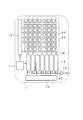
- FIG. 3 (a) shows the cross-sectional structure of the solid-state imaging device 1
- FIG. 3 (b) shows the planar structure of the solid-state imaging device 1.
- the solid-state imaging device 1 has a structure in which two substrates (first substrate 20 and second substrate 21) on which circuit elements (a photoelectric conversion unit, a transistor, a capacitor, and the like) constituting the unit pixel 1-5 are arranged overlap each other.
- Have Circuit elements constituting the unit pixel 1-5 are distributed and arranged on the first substrate 20 and the second substrate 21.
- the first substrate 20 and the second substrate 21 are electrically connected so that an electrical signal can be exchanged between the two substrates when the unit pixel 1-5 is driven.
- a photoelectric conversion unit is formed on the main surface side on which the light L is irradiated. The irradiated light is incident on the photoelectric conversion unit.
- the main surface opposite to the main surface irradiated with the light L is provided with a number of micropads 22 as electrodes for connection with the second substrate 21. Is formed.
- One micropad 22 is arranged for each pixel or for each of a plurality of pixels.
- many of the main surfaces facing the first substrate 20 are electrodes for connection with the first substrate 20 at positions corresponding to the micropads 22.
- the micropad 23 is formed.
- a micro bump 24 is formed between the micro pad 22 and the micro pad 23.
- the first substrate 20 and the second substrate 21 are arranged so that the micropad 22 and the micropad 23 face each other, and the micropad 22 and the micropad 23 are electrically connected by the microbump 24. It is integrated.
- the micropad 22, the microbump 24, and the micropad 23 constitute a connection portion that electrically connects the first substrate 20 and the second substrate 21.
- a signal based on the signal charge generated in the photoelectric conversion unit disposed on the first substrate 20 is output to the second substrate 21 through the micropad 22, the microbump 24, and the micropad 23.
- a micropad 25 having the same structure as the micropad 22 is formed on the periphery of the main surface opposite to the main surface on which the light L is irradiated. ing.
- a micropad 26 having the same structure as the micropad 23 is formed at a position corresponding to the micropad 25 on the main surface facing the first substrate 20.
- Micro bumps 27 are formed between the micro pad 25 and the micro pad 26.
- a circuit element disposed on the first substrate 20 or a power supply voltage for driving the circuit element disposed on the second substrate 21 is supplied to the first substrate 20 via the micropad 25, the microbump 27, and the micropad 26. To the second substrate 21 or from the second substrate 21 to the first substrate 20.
- a pad 28 used as an interface with a system other than the first substrate 20 and the second substrate 21 is formed in the periphery of one of the two main surfaces of the second substrate 21.
- a through electrode penetrating the second substrate 21 may be provided, and the through electrode may be used as an electrode for external connection.
- the areas of the main surfaces of the first substrate 20 and the second substrate 21 are different, but the areas of the main surfaces of the first substrate 20 and the second substrate 21 may be the same.
- the micropad (first electrode) provided on the surface of the first substrate 20 and the micropad (second electrode) provided on the surface of the second substrate 21 are directly bonded without providing the micro bumps.
- the first substrate 20 and the second substrate 21 may be connected.
- the circuit elements constituting the unit pixel 1-5 are distributed on the first substrate 20 and the second substrate 21.
- the control signal generation circuit 1-1, vertical readout control circuit 1-2, horizontal readout control circuit 1-3, column signal processing unit 1-6, and output circuit 1-8 other than the unit pixel 1-5 are each first. It may be disposed on either the substrate 20 or the second substrate 21.
- the circuit elements constituting each of the control signal generation circuit 1-1, the vertical readout control circuit 1-2, the horizontal readout control circuit 1-3, the column signal processing unit 1-6, and the output circuit 1-8 are the first substrate. 20 and the second substrate 21 may be distributed.
- the configuration other than the unit pixel 1-5 it may be necessary to send and receive signals between the first substrate 20 and the second substrate 21, but as with the unit pixel 1-5, micropads and microbumps are used.
- the first substrate 20 and the second substrate 21 can be connected, or the micropads can be directly connected to connect the first substrate 20 and the second substrate 21.
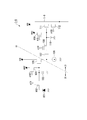
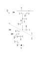
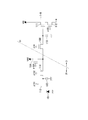
- FIG. 4 shows the configuration of the unit pixels 1-5.
- the unit pixel 1-5 includes a photoelectric conversion unit 101, a transfer transistor 102, an FD (floating diffusion) 103, an FD reset transistor 104, a first amplification transistor 105, a current source 106, a clamp capacitor 107, and sampling.
- the transistor 108, the clamp transistor 109, the analog memory 110, the second amplification transistor 111, and the selection transistor 112 are included.
- One end of the photoelectric conversion unit 101 is grounded.
- the drain terminal of the transfer transistor 102 is connected to the other end of the photoelectric conversion unit 101.
- the gate terminal of the transfer transistor 102 is connected to the vertical read control circuit 1-2, and the transfer pulse ⁇ TX is supplied.
- One end of the FD 103 is connected to the source terminal of the transfer transistor 102, and the other end of the FD 103 is grounded.
- the drain terminal of the FD reset transistor 104 is connected to a reference voltage source that supplies a reference voltage VREF, and the source terminal of the FD reset transistor 104 is connected to the source terminal of the transfer transistor 102.
- the gate terminal of the FD reset transistor 104 is connected to the vertical read control circuit 1-2, and the FD reset pulse ⁇ RST is supplied.
- the drain terminal of the first amplification transistor 105 is connected to a power supply that supplies a power supply voltage VDD.
- a gate terminal which is an input portion of the first amplification transistor 105 is connected to the source terminal of the transfer transistor 102.
- One end of the current source 106 is connected to the source terminal of the first amplification transistor 105, and the other end of the current source 106 is grounded.
- the current source 106 may be configured by a transistor having a drain terminal connected to the source terminal of the first amplification transistor 105, a source terminal grounded, and a gate terminal connected to the vertical readout control circuit 1-2.
- One end of the clamp capacitor 107 is connected to the source terminal of the first amplification transistor 105 and one end of the current source 106.
- the drain terminal of the sampling transistor 108 is connected to the other end of the clamp capacitor 107.
- the gate terminal of the sampling transistor 108 is connected to the vertical readout control circuit 1-2, and the sample pulse ⁇ SH is supplied.
- the drain terminal of the clamp transistor 109 is connected to a reference voltage source that supplies the reference voltage VREF, and the source terminal of the clamp transistor 109 is connected to the source terminal of the sampling transistor 108.
- the gate terminal of the clamp transistor 109 is connected to the vertical read control circuit 1-2, and a clamp & memory reset pulse ⁇ CL is supplied.
- the drain terminal of the second amplification transistor 111 is connected to a power supply that supplies a power supply voltage VDD.
- a gate terminal which is an input part of the second amplification transistor 111 is connected to a source terminal of the sampling transistor 108.
- the drain terminal of the selection transistor 112 is connected to the source terminal of the second amplification transistor 111, and the source terminal of the selection transistor 112 is connected to the vertical signal line 1-9.
- the gate terminal of the selection transistor 112 is connected to the vertical read control circuit 1-2, and the selection pulse ⁇ SEL is supplied.
- the polarity may be reversed, and the source terminal and the drain terminal may be reversed.
- the photoelectric conversion unit 101 is, for example, a photodiode, generates (generates) signal charges based on incident light, holds and stores the generated (generated) signal charges, and outputs the signal charges after a predetermined period of time has elapsed.
- the transfer transistor 102 is a transistor that transfers the signal charge accumulated in the photoelectric conversion unit 101 to the FD 103. The on / off of the transfer transistor 102 is controlled by the transfer pulse ⁇ TX from the vertical read control circuit 1-2.
- the FD 103 is a capacitor that temporarily holds and accumulates signal charges transferred from the photoelectric conversion unit 101.
- the FD reset transistor 104 is a transistor that resets the FD 103. On / off of the FD reset transistor 104 is controlled by an FD reset pulse ⁇ RST from the vertical read control circuit 1-2. It is also possible to reset the photoelectric conversion unit 101 by simultaneously turning on the FD reset transistor 104 and the transfer transistor 102. To reset the FD103 / photoelectric conversion unit 101, control the amount of charge accumulated in the FD103 / photoelectric conversion unit 101 to set the state (potential) of the FD103 / photoelectric conversion unit 101 to the reference state (reference potential, reset level). It is to be.
- the first amplification transistor 105 is a transistor that outputs an amplified signal obtained by amplifying a signal based on the signal charge stored in the FD 103, which is input to the gate terminal, from the source terminal.
- the current source 106 functions as a load for the first amplification transistor 105 and supplies a current for driving the first amplification transistor 105 to the first amplification transistor 105.
- the first amplification transistor 105 and the current source 106 constitute a source follower circuit.
- the clamp capacitor 107 is a capacitor that clamps (fixes) the voltage level of the amplified signal output from the first amplification transistor 105.
- the sampling transistor 108 is a transistor that samples and holds the voltage level at the other end of the clamp capacitor 107 and accumulates it in the analog memory 110. On / off of the sampling transistor 108 is controlled by a sample pulse ⁇ SH from the vertical read control circuit 1-2.
- the clamp transistor 109 is a transistor that resets the analog memory 110.
- the reset of the analog memory 110 is to set the state (potential) of the analog memory 110 to the reference state (reference potential, reset level) by controlling the amount of charge accumulated in the analog memory 110.
- the analog memory 110 is a capacitor that holds and stores an analog signal sampled and held by the sampling transistor 108.
- the capacity value of the analog memory 110 is set larger than the capacity value of the FD103.
- a MIM (Metal Insulator Metal) capacity or a MOS (Metal Oxide Semiconductor) capacity which is a capacity with a small leakage current (dark current) per unit area. Thereby, resistance to noise is improved, and a high-quality signal can be obtained.
- the second amplifying transistor 111 is a transistor that outputs an amplified signal obtained by amplifying a signal based on the signal charge stored in the analog memory 110, which is input to the gate terminal, from the source terminal.
- the selection transistor 112 is a transistor that selects the unit pixel 1-5 and outputs the signal amplified by the second amplification transistor 111 to the vertical signal line 1-9. ON / OFF of the selection transistor 112 is controlled by a selection pulse ⁇ SEL from the vertical read control circuit 1-2.
- the broken line D1 in FIG. 4 shows the boundary line between the first substrate 20 and the second substrate 21.
- a photoelectric conversion unit 101 On the first substrate 20, a photoelectric conversion unit 101, a transfer transistor 102, an FD 103, an FD reset transistor 104, and a first amplification transistor 105 are arranged.
- a current source 106 On the second substrate 21, a clamp capacitor 107, a sampling transistor 108, a clamp transistor 109, an analog memory 110, a second amplification transistor 111, and a selection transistor 112 are arranged.
- the amplified signal output from the first amplification transistor 105 on the first substrate 20 is output to the second substrate 21 via the micropad 22, the microbump 24, and the micropad 23.
- the power supply voltage VDD and the reference voltage VREF are exchanged between the first substrate 20 and the second substrate 21 through the micropad 25, the microbump 27, and the micropad 26.
- connection portion including the micropad 22, the microbump 24, and the micropad 23 is arranged in a path between the source terminal of the first amplification transistor 105 and the drain terminal of the current source 106 and one end of the clamp capacitor 107.
- the connecting portion may be disposed anywhere on the electrically connected path from the photoelectric conversion element 101 to the analog memory 110.
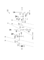
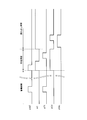
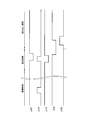
- FIG. 5 shows an example of the boundary line between the first substrate 20 and the second substrate 21.
- Broken lines D1 to D5 show examples that can be used as boundary lines between the first substrate 20 and the second substrate 21.
- the boundary line between the first substrate 20 and the second substrate 21 may be any of the broken lines D1 to D5.
- the photoelectric conversion element 101 is disposed on the first substrate 20 and the analog memory 110 is disposed on the second substrate. It should be done.
- the broken line D1 is as described above.
- a connection portion is disposed on a path between the other end of the photoelectric conversion element 101 and the drain terminal of the transfer transistor 102.
- a connection portion is disposed on a path between the source terminal of the transfer transistor 102, one end of the FD 103, the source terminal of the FD reset transistor 104, and the gate terminal of the first amplification transistor 105.
- connection portion is disposed in a path between the other end of the clamp capacitor 107 and the drain terminal of the sampling transistor 108.
- a connection portion is disposed on a path between the source terminal of the sampling transistor 108, the source terminal of the clamp transistor 109, one end of the analog memory 110, and the gate terminal of the second amplification transistor 111.
- the sampling transistor 108 and the analog memory 110 constitute a signal holding unit that holds the signal output from the photoelectric conversion unit 101.
- a signal corresponding to the signal charge output from the photoelectric conversion unit 101 is input to the drain terminal (first terminal) of the sampling transistor 108, the sampling transistor 108 samples and holds the signal input to the drain terminal.
- the sampled and held signal is output from the source terminal (second terminal).
- the analog memory 110 holds a signal output from the source terminal of the sampling transistor 108.
- the FD reset transistor 104 has a drain terminal (third terminal) connected to the reference voltage source that supplies the reference voltage VREF, and a source terminal (fourth terminal) connected via the transfer transistor 102. It is connected to the photoelectric conversion unit 101 and resets the photoelectric conversion unit 101. Further, as described in detail below, the FD reset transistor 104 sets the potential of one end of the FD 103 and the gate terminal of the first amplification transistor 105 during a read period in which a signal based on the signal charge stored in the analog memory 110 is read.
- the potential of the drain terminal of the sampling transistor 108 is fixed by fixing the potential to a fixed potential (VREF) supplied from the reference voltage source. For this reason, it is possible to suppress fluctuations in the potential of the drain terminal of the sampling transistor 108 due to noise such as 1 / f noise, and noise resistance can be improved.
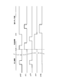
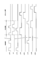
- FIG. 6 shows control signals supplied from the vertical readout control circuit 1-2 to the unit pixels 1-5 for each row.
- the unit pixels 1-5 are indicated, they are described as all pixels.
- the accumulation period is a period common to all the pixels, and the operation is simultaneously performed on all the pixels.
- the transfer pulse ⁇ TX and the FD reset pulse ⁇ RST change from the L (Low) level to the H (High) level
- the transfer transistor 102 and the FD reset transistor 104 are turned on.
- the photoelectric conversion units 101 of all the pixels are reset.
- the transfer pulse ⁇ TX and the FD reset pulse ⁇ RST change from the H level to the L level
- the transfer transistor 102 and the FD reset transistor 104 are turned off.
- the resetting of all the pixels is completed, and the exposure (accumulation of signal charges) of all the pixels is started at the same time (the exposure period starts).
- the transfer period is a period common to all the pixels, and the operation is simultaneously performed on all the pixels.
- the FD reset pulse ⁇ RST changes from the L level to the H level
- the FD reset transistor 104 is turned on.
- the FDs 103 of all the pixels are reset.
- the clamp transistor 109 is turned on.
- the analog memory 110 of all pixels is reset.
- the sampling transistor 108 is turned on.
- the potential at the other end of the clamp capacitor 107 of all the pixels is reset to the reference voltage VREF, and the sampling transistor 108 of all the pixels starts to sample and hold the potential at the other end of the clamp capacitor 107.
- the FD reset pulse ⁇ RST changes from the H level to the L level
- the FD reset transistor 104 is turned off.
- the clamp transistor 109 is turned off.
- the reset of the analog memory 110 of all the pixels is completed.
- the clamp capacitor 107 clamps the amplified signal (the amplified signal after the reset of the FD 103) output from the first amplification transistor 105.
- the transfer transistor 102 is turned on.
- the signal charges accumulated in the photoelectric conversion units 101 of all the pixels are transferred to the FD 103 via the transfer transistor 102 and accumulated in the FD 103.
- the transfer transistor 102 is turned off.
- the sampling transistor 108 is turned off.
- the sampling transistors 108 of all the pixels finish sampling and holding the potential at the other end of the clamp capacitor 107.
- the clamp capacitor 107 clamps the amplified signal output from the first amplification transistor 105 (the amplified signal after the signal charge is transferred from the photoelectric conversion unit 101 to the FD 103).
- the potential of the gate terminal of the first amplification transistor 105 connected to one end of the clamp capacitor 107 is fixed, the potential of one end of the clamp capacitor is also fixed, and the potential of the drain terminal of the sampling transistor 108 is also fixed.
- the FD reset transistor 104 remains on.
- the selection transistor 112 is turned on.
- the pixel signal level based on the signal charge accumulated in the analog memory 110 is output to the vertical signal line 1-9.
- the clamp transistor 109 is turned on when the clamp & memory reset pulse ⁇ CL changes from the L level to the H level.
- the analog memory 110 is reset and a reset level is output to the vertical signal line 1-9.
- the selection transistor 112 is turned off.
- the clamp transistor 109 is turned off.
- the column signal processor 1-6 calculates a difference between the read pixel signal level and the reset level, thereby removing read noise generated when reading the pixel signal from the analog memory 110.
- the above operations are sequentially performed row by row, so that the pixel signals of all the pixels are read out.
- the signal charges accumulated in the photoelectric conversion units 101 of all the pixels are transferred in a lump, so that the simultaneous accumulation of signal charges can be realized.
- the FD reset transistor 104 performs sampling by fixing the potential of one end of the FD 103 and the gate terminal of the first amplification transistor 105 to a potential corresponding to the fixed potential during the readout period.
- the potential of the drain terminal of the transistor 108 is fixed. For this reason, it is possible to suppress fluctuations in the potential of the drain terminal of the sampling transistor 108 due to noise such as 1 / f noise, and noise resistance can be improved.
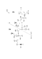
- FIG. 7 shows another example of the configuration of the unit pixel 1-5. Compared with the configuration shown in FIG. 4, the clamp capacitor 107 and the clamp transistor 109 are omitted in FIG. 7, and the drain terminal of the sampling transistor 108 is connected to the source terminal of the first amplification transistor 105 and one end of the current source 106. ing.
- the configuration other than the above is the same as the configuration shown in FIG.
- connection portion including the micropad 22, the microbump 24, and the micropad 23 is arranged in a path between the source terminal of the first amplification transistor 105 and the drain terminal of the current source 106 and the drain terminal of the sampling transistor 108.
- the connecting portion may be disposed anywhere on the electrically connected path from the photoelectric conversion element 101 to the analog memory 110.
- FIG. 8 shows an example of the boundary line between the first substrate 20 and the second substrate 21.
- Broken lines D1 to D5 show examples that can be used as boundary lines between the first substrate 20 and the second substrate 21.
- the boundary line between the first substrate 20 and the second substrate 21 may be any of the broken lines D1 to D5.
- the photoelectric conversion element 101 is disposed on the first substrate 20 and the analog memory 110 is disposed on the second substrate. It should be done.
- the broken line D1 is as described above.
- a connection portion is disposed on a path between the other end of the photoelectric conversion element 101 and the drain terminal of the transfer transistor 102.
- a connection portion is disposed on a path between the source terminal of the transfer transistor 102, one end of the FD 103, the source terminal of the FD reset transistor 104, and the gate terminal of the first amplification transistor 105.
- a connection portion is disposed in the path between the source terminal of the amplification transistor 105 and one end of the current source 106 and the drain terminal of the sampling transistor 108.
- the sampling transistor 108 A connection portion is disposed on a path between the source terminal and one end of the analog memory 110 and the gate terminal of the second amplification transistor 111.
- FIG. 9 shows control signals supplied from the vertical readout control circuit 1-2 to the unit pixels 1-5 for each row. In the following, the operation different from the operation shown in FIG. 6 will be mainly described.
- the operation during the accumulation period is the same as that shown in FIG.
- the transfer period after the FDs 103 of all the pixels are reset, the signal charges accumulated in the photoelectric conversion unit 101 are transferred to the FD 103 via the transfer transistor 102 and accumulated in the FD 103.
- the amplified signal output from the source terminal of the first amplification transistor 105 at this time is input to the analog memory 110, and signal charges based on the amplified signal are accumulated in the analog memory 110.
- the FD reset pulse ⁇ RST changes from the L level to the H level, so that the FD reset transistor 104 is turned on.
- the potential of one end of the FD 103 and the gate terminal of the first amplification transistor 105 is fixed to a potential corresponding to the fixed potential (VREF) supplied from the reference voltage source.
- the potential of the drain terminal of the sampling transistor 108 is also fixed.
- the selection transistor 112 is turned on.
- the pixel signal level based on the signal charge accumulated in the analog memory 110 is output to the vertical signal line 1-9.
- the sampling transistor 108 is turned on.
- the FD reset transistor 104 is on and the FD 103 is reset, an amplified signal based on the potential of one end of the FD 103 after reset is output from the source terminal of the first amplification transistor 105.
- the amplified signal is input to the analog memory 110, and signal charges based on the amplified signal are accumulated in the analog memory 110.
- the selection transistor 112 is on, a reset level based on the potential at one end of the FD 103 after reset is output to the vertical signal line 1-9.
- the selection transistor 112 is turned off.
- the sampling transistor 108 is turned off when the sample pulse ⁇ SH changes from the H level to the L level.
- the configuration of the imaging apparatus according to the present embodiment is the same as the configuration of the imaging apparatus according to the first embodiment.
- the current source 106 can operate by switching between three modes: an off mode, a current setting mode, and a low impedance setting mode.
- FIG. 10 shows the control signal supplied to the unit pixel 1-5 for each row from the vertical readout control circuit 1-2 and the mode of the current source 106. In the following, the operation different from the operation shown in FIG. 6 will be mainly described.
- the current source 106 is set to the off mode and stops operating. In the transfer period, the current source 106 is set to the current setting mode and outputs a current for driving the first amplification transistor 105.
- the impedance of the current source 106 when set in the current setting mode is higher than the impedance of the current source 106 when set in the low impedance setting mode.
- the FD reset transistor 104 is off.
- the current source 106 is set to the low impedance setting mode.
- the potential at one end of the current source 106 connected to the source terminal of the first amplification transistor 105 and one end of the clamp capacitor 107 is substantially the same as the potential at the other end of the current source 106.
- the current source 106 is composed of a transistor, the potentials of the drain terminal and the source terminal of the current source 106 are substantially the same.
- the potential at one end of the clamp capacitor 107 is fixed to the potential at the other end of the current source 106, that is, substantially the same as the ground potential. Therefore, the potential of the drain terminal of the sampling transistor 108 is also fixed.
- the potential of the drain terminal of the sampling transistor 108 is fixed by fixing the potentials of the one end and the other end of the current source 106 to substantially the same potential during the reading period. . For this reason, it is possible to suppress fluctuations in the potential of the drain terminal of the sampling transistor 108 due to noise such as 1 / f noise, and noise resistance can be improved.
- the current source 106 may operate in the low impedance setting mode instead of turning on the FD reset transistor 104 during the readout period.
- the configuration of the imaging device according to the present embodiment is the same as the configuration of the imaging device according to the first embodiment except for the unit pixels 1-5.
- FIG. 11 shows the configuration of the unit pixel 1-5 in the present embodiment.
- the position where the clamp transistor 109 is arranged is different from the unit pixel 1-5 shown in FIG.
- the source terminal (third terminal) of the clamp transistor 109 is connected to the other end of the clamp capacitor 107 and the drain terminal of the sampling transistor 108, and the drain terminal (fourth terminal) of the clamp transistor 109 is the reference voltage.
- the reference voltage Connected to a reference voltage source that supplies VREF.
- the configuration other than the above is the same as the configuration of the unit pixel 1-5 shown in FIG.
- connection portion including the micropad 22, the microbump 24, and the micropad 23 is arranged in a path between the source terminal of the first amplification transistor 105 and the drain terminal of the current source 106 and one end of the clamp capacitor 107.
- the connecting portion may be disposed anywhere on the electrically connected path from the photoelectric conversion element 101 to the analog memory 110.
- FIG. 12 shows an example of the boundary line between the first substrate 20 and the second substrate 21.
- Broken lines D1 to D5 show examples that can be used as boundary lines between the first substrate 20 and the second substrate 21.
- the boundary line between the first substrate 20 and the second substrate 21 may be any of the broken lines D1 to D5.
- the photoelectric conversion element 101 is disposed on the first substrate 20 and the analog memory 110 is disposed on the second substrate. It should be done.
- the broken line D1 is as described above.
- a connection portion is disposed on a path between the other end of the photoelectric conversion element 101 and the drain terminal of the transfer transistor 102.
- a connection portion is disposed on a path between the source terminal of the transfer transistor 102, one end of the FD 103, the source terminal of the FD reset transistor 104, and the gate terminal of the first amplification transistor 105.
- a connection portion is disposed on the path between the source terminal of the clamp transistor 109 and the other end of the clamp capacitor 107 and the drain terminal of the sampling transistor 108.
- the sampling transistor 108 is provided.
- the connection portion is disposed in a path between the source terminal of the first memory terminal and one end of the analog memory 110 and the gate terminal of the second amplification transistor 111.
- the clamp transistor 109 fixes the potential of the drain terminal of the sampling transistor to a potential corresponding to the fixed potential (VREF) supplied from the reference voltage source during the readout period.
- FIG. 13 shows control signals supplied from the vertical readout control circuit 1-2 to the unit pixels 1-5 for each row.
- the operation different from the operation shown in FIG. 6 will be mainly described.
- the operation in the accumulation period and the transfer period is the same as that shown in FIG.
- the FD reset transistor 104 is off.
- the clamp transistor 109 is turned on when the clamp & memory reset pulse ⁇ CL changes from the L level to the H level.
- the potential of the drain terminal of the sampling transistor 108 is fixed to a potential corresponding to the fixed potential (VREF) supplied from the reference voltage source.
- the selection transistor 112 is turned on.
- the pixel signal level based on the signal charge accumulated in the analog memory 110 is output to the vertical signal line 1-9.
- the selection transistor 112 is turned off.
- the sampling transistor 108 is turned off when the sample pulse ⁇ SH changes from the H level to the L level.
- the clamp transistor 109 fixes the potential of the drain terminal of the sampling transistor 108 to a potential corresponding to the fixed potential during the readout period. For this reason, it is possible to suppress fluctuations in the potential of the drain terminal of the sampling transistor 108 due to noise such as 1 / f noise, and noise resistance can be improved.
- the configuration of the imaging apparatus according to the present embodiment is the same as the configuration of the imaging apparatus according to the third embodiment except for the unit pixels 1-5.
- FIG. 14 shows a circuit configuration of two unit pixels 1-5 adjacent in the vertical direction.
- Unit pixels 1-5 include photoelectric conversion units 101-1 and 101-2, transfer transistors 102-1 and 102-2, FD103, FD reset transistor 104, first amplification transistor 105, A current source 106, a clamp capacitor 107, sampling transistors 108-1 and 108-2, a clamp transistor 109, analog memories 110-1 and 110-2, second amplification transistors 111-1 and 111-2, Selection transistors 112-1 and 112-2 are included.
- FIG. 14 includes a circuit element of the first unit pixel and a circuit element of the second unit pixel.
- the first unit pixel includes a photoelectric conversion unit 101-1, a transfer transistor 102-1, an FD 103, an FD reset transistor 104, a first amplification transistor 105, a current source 106, a clamp capacitor 107, and a sampling transistor. 108-1, a clamp transistor 109, an analog memory 110-1, a second amplification transistor 111-1, and a selection transistor 112-1.
- the second unit pixel includes a photoelectric conversion unit 101-2, a transfer transistor 102-2, an FD 103, an FD reset transistor 104, a first amplification transistor 105, a current source 106, a clamp capacitor 107, and a sampling transistor. 108-2, a clamp transistor 109, an analog memory 110-2, a second amplification transistor 111-2, and a selection transistor 112-2.
- the FD 103, the FD reset transistor 104, the first amplification transistor 105, the current source 106, the clamp capacitor 107, and the clamp transistor 109 are shared by the first unit pixel and the second unit pixel.
- connection relationship of the circuit elements constituting each unit pixel 1-5 is the same as the connection relationship of the circuit elements in the unit pixel 1-5 shown in FIG.
- the source terminals of the transfer transistors 102-1 and 102-2 are commonly connected to one end of the FD 103, the source terminal of the FD reset transistor 104, and the gate terminal of the first amplification transistor 105.
- the drain terminals of the sampling transistors 108-1 and 108-2 are commonly connected to the other end of the clamp capacitor 107 and the source terminal of the clamp transistor 109.
- a transfer pulse ⁇ TX1 is supplied from the vertical read control circuit 1-2 to the gate terminal of the transfer transistor 102-1, and a transfer pulse ⁇ TX2 is supplied from the vertical read control circuit 1-2 to the gate terminal of the transfer transistor 102-2.
- a sampling pulse ⁇ SH1 is supplied from the vertical readout control circuit 1-2 to the gate terminal of the sampling transistor 108-1, and a sampling pulse ⁇ SH2 is supplied from the vertical readout control circuit 1-2 to the gate terminal of the sampling transistor 108-2.
- the selection pulse ⁇ SEL1 is supplied from the vertical readout control circuit 1-2 to the gate terminal of the selection transistor 112-1, and the selection pulse ⁇ SEL2 is supplied from the vertical readout control circuit 1-2 to the gate terminal of the selection transistor 112-2. .
- connection portion including the micropad 22, the microbump 24, and the micropad 23 is disposed in a path between the source terminal of the first amplification transistor 105, the drain terminal of the current source 106, and one end of the clamp capacitor 107.
- the connecting portion may be disposed anywhere on the electrically connected path from the photoelectric conversion element 101 to the analog memory 110.
- FIG. 15 shows an example of the boundary line between the first substrate 20 and the second substrate 21.
- Broken lines D1 to D5 show examples that can be used as boundary lines between the first substrate 20 and the second substrate 21.
- the boundary line between the first substrate 20 and the second substrate 21 may be any of the broken lines D1 to D5.
- the photoelectric conversion elements 101-1 and 101-2 are arranged on the first substrate 20, and the second substrate It is sufficient if the analog memories 110-1 and 110-2 are arranged.
- the broken line D1 is as described above.
- a connection portion is disposed on a path between the other ends of the photoelectric conversion elements 101-1 and 101-2 and the drain terminal of the transfer transistor 102.
- a connection portion is connected to a path between the source terminals of the transfer transistors 102-1 and 102-2, one end of the FD 103, the source terminal of the FD reset transistor 104, and the gate terminal of the first amplification transistor 105. Is placed.
- a connection portion is disposed on the path between the source terminal of the clamp transistor 109 and the other end of the clamp capacitor 107 and the drain terminals of the sampling transistors 108-1 and 108-2, and the broken line D5 indicates. In the example, it is connected to a path between the source terminals of the sampling transistors 108-1 and 18-2 and one end of the analog memories 110-1 and 110-2 and the gate terminals of the second amplification transistors 111-1 and 111-2. Parts are arranged.
- FIG. 16 shows control signals supplied to the unit pixels 1-5 for each row from the vertical readout control circuit 1-2.
- the operation will be described in units of two unit pixels 1-5 shown in FIG.
- each unit pixel 1-5 in the accumulation period is the same as the operation of the unit pixel 1-5 in the accumulation period shown in FIG.
- Transfer period operation In the transfer period, the reset of the FD 103 common to the two unit pixels 1-5 and the transfer of the signal charges accumulated in the photoelectric conversion units 101-1 and 101-2 of the two unit pixels 1-5 are performed. The operation including this is performed for each unit pixel. After the FD 103 is reset and the signal charges of the first unit pixel are transferred, the FD 103 is reset and the signal charges of the second unit pixel are transferred. The operation of each unit pixel 1-5 in the transfer period is the same as the operation of the unit pixel 1-5 in the transfer period shown in FIG.
- the clamp transistor 109 fixes the potentials of the drain terminals of the sampling transistors 108-1 and 108-2 to a potential corresponding to the fixed potential during the readout period. For this reason, it is possible to suppress fluctuations in the potentials of the drain terminals of the sampling transistors 108-1 and 108-2 due to noise such as 1 / f noise, and noise resistance can be improved.
- the clamp transistor 109 is shared by the plurality of unit pixels 1-5, so that the circuit area can be reduced. .
- an example is shown in which two unit pixels 1-5 share some circuit elements including the clamp transistor 109, but three or more unit pixels 1-5 share some circuit elements. May be.
- the configuration of the imaging device according to the present embodiment is the same as the configuration of the imaging device according to the first embodiment except for the unit pixels 1-5.
- FIG. 17 shows a configuration of the unit pixel 1-5 in the present embodiment.
- the first amplification transistor 105, the current source 106, the clamp capacitor 107, and the clamp transistor 109 are deleted, the second transfer transistor 114 is added, and the transfer transistor 102 is replaced with the first transfer transistor 113. This is different from the unit pixel 1-5 shown in FIG.
- the drain terminal of the second transfer transistor 114 is connected to the source terminal of the first transfer transistor 113 and one end of the FD 103, and the source terminal of the second transfer transistor 114 is connected to the drain terminal of the sampling transistor 108.
- the gate terminal of the second transfer transistor 113 is connected to the vertical read control circuit 1-2, and the transfer pulse ⁇ TX2 is supplied. Further, the transfer pulse ⁇ TX1 is supplied to the gate terminal of the first transfer transistor 113 from the vertical read control circuit 1-2.
- the configuration other than the above is the same as the configuration of the unit pixel 1-5 shown in FIG.
- connection portion including the micropad 22, the microbump 24, and the micropad 23 is a path between the source terminal of the second transfer transistor 114, the source terminal of the FD reset transistor 104, and the drain terminal of the sampling transistor 108.
- the connecting portion may be disposed anywhere on the electrically connected path from the photoelectric conversion element 101 to the analog memory 110.
- FIG. 18 shows an example of the boundary line between the first substrate 20 and the second substrate 21.
- Broken lines D1 to D5 show examples that can be used as boundary lines between the first substrate 20 and the second substrate 21.
- the boundary line between the first substrate 20 and the second substrate 21 may be any of the broken lines D1 to D5.
- the photoelectric conversion element 101 is disposed on the first substrate 20 and the analog memory 110 is disposed on the second substrate. It should be done.
- the broken line D1 is as described above.
- a connection portion is disposed on a path between the other end of the photoelectric conversion element 101 and the drain terminal of the first transfer transistor 113.
- a connection portion is disposed on a path between the source terminal of the first transfer transistor 113 and one end of the FD 103 and the drain terminal of the second transfer transistor 114.
- a connection portion is disposed in the path between the source terminal of the second transfer transistor 114, the source terminal of the FD reset transistor 104, and the drain terminal of the sampling transistor 108, and in the example indicated by the broken line D5, A connecting portion is disposed on a path between the source terminal of the sampling transistor 108 and one end of the analog memory 110 and the gate terminal of the second amplification transistor 111.
- FIG. 19 shows control signals supplied to the unit pixels 1-5 for each row from the vertical readout control circuit 1-2.
- the accumulation period is a period common to all the pixels, and the operation is simultaneously performed on all the pixels.
- the FD reset pulse ⁇ RST, the transfer pulse ⁇ TX2, and the sample pulse ⁇ SH are at the H level, and the FD reset transistor 104, the second transfer transistor 114, and the sampling transistor 108 are on.
- the FD 103 and the analog memory 110 of all the pixels are reset.
- the first transfer transistor 113 is turned on. As a result, the photoelectric conversion units 101 of all the pixels are reset. Subsequently, when the transfer pulse ⁇ TX1 changes from the H level to the L level, the first transfer transistor 113 is turned off. As a result, the resetting of all the pixels is completed, and the exposure (accumulation of signal charges) of all the pixels is started at the same time (the exposure period starts).
- the transfer period is a period common to all the pixels, and the operation is simultaneously performed on all the pixels.
- the transfer pulse ⁇ TX2 changes from H level to L level
- the second transfer transistor 114 is turned off.
- the transfer pulse ⁇ TX1 changes from the L level to the H level
- the first transfer transistor 113 is turned on.
- the signal charge accumulated in the photoelectric conversion unit 101 is transferred to the FD 103 via the first transfer transistor 113 and accumulated in the FD 103.
- exposure of all pixels accumulation of signal charge
- the FD reset transistor ⁇ RST changes from the H level to the L level
- the FD reset transistor 104 is turned off.
- the transfer pulse ⁇ TX1 changes from the H level to the L level
- the first transfer transistor 113 is turned off.
- the transfer pulse ⁇ TX2 changes from the L level to the H level
- the second transfer transistor 114 is turned on.
- the signal charge stored in the FD 103 is transferred to the analog memory 110 via the second transfer transistor 114 and the sampling transistor 108 and stored in the analog memory 110.
- the sampling transistor 108 is turned off.
- the FD reset pulse ⁇ RST changes from the L level to the H level, the FD reset transistor 104 is turned on.
- the potential of the drain terminal of the sampling transistor 108 is fixed to a potential corresponding to the fixed potential (VREF) supplied from the reference voltage source.
- the selection transistor 112 is turned on. As a result, the pixel signal level based on the signal charge accumulated in the analog memory 110 is output to the vertical signal line 1-9.
- the sampling transistor 108 is turned on.
- the analog memory 110 is reset and a reset level is output to the vertical signal line 1-9.
- the selection pulse ⁇ SEL changes from the H level to the L level, the selection transistor 112 is turned off.
- the column signal processor 1-6 calculates a difference between the read pixel signal level and the reset level, thereby removing read noise generated when reading the pixel signal from the analog memory 110.
- the above operations are sequentially performed row by row, so that the pixel signals of all the pixels are read out.
- the signal charges accumulated in the photoelectric conversion units 101 of all the pixels are transferred in a lump, so that the simultaneous accumulation of signal charges can be realized.
- the FD reset transistor 104 fixes the potential of the drain terminal of the sampling transistor 108 to a potential corresponding to the fixed potential during the reading period. For this reason, it is possible to suppress fluctuations in the potential of the drain terminal of the sampling transistor 108 due to 1 / f noise and the like, and noise resistance can be improved.
- the embodiments of the present invention have been described in detail with reference to the drawings.
- the specific configuration is not limited to the above-described embodiments, and includes design changes and the like without departing from the gist of the present invention.
- the configuration of the solid-state imaging device in which two substrates are connected by the connection unit is shown, but three or more substrates may be connected by the connection unit.
- two of the three or more substrates correspond to the first substrate and the second substrate.
- Each aspect of the present invention can be widely applied to solid-state imaging devices and imaging devices.
- the potential of the first terminal of the sampling transistor is fixed to a potential corresponding to a predetermined fixed potential. It is possible to suppress fluctuations in the potential of the first terminal of the sampling transistor due to the above, and noise resistance can be improved.
Landscapes
- Engineering & Computer Science (AREA)
- Multimedia (AREA)
- Signal Processing (AREA)
- Physics & Mathematics (AREA)
- Power Engineering (AREA)
- Electromagnetism (AREA)
- Condensed Matter Physics & Semiconductors (AREA)
- General Physics & Mathematics (AREA)
- Computer Hardware Design (AREA)
- Microelectronics & Electronic Packaging (AREA)
- Transforming Light Signals Into Electric Signals (AREA)
- Solid State Image Pick-Up Elements (AREA)
Abstract
Provided is a solid-state imaging device in which a first substrate and a second substrate which have circuit elements constituting pixels arranged thereon are electrically connected, wherein the pixels have: a photoelectric conversion unit arranged on the first substrate, for outputting a signal on the basis of entering light; a sampling transistor, which is arranged on the second substrate and which has a gate electrode, a source electrode, and a drain electrode, a signal output from the photoelectric conversion unit being input to a first terminal that is either the source electrode or the drain electrode, for sampling and holding the signal input to the first terminal, and outputting the sampled and held signal to a second terminal that is the other of the source terminal and the drain terminal; and a capacitor arranged on the second substrate, for holding the signal output from the second terminal. During read intervals in which a signal held in the capacitor is read, the potential of the first terminal is fixed at a potential according to a prescribed fixed potential.
Description
本発明は、画素を構成する回路素子が配置された第1の基板と第2の基板とが電気的に接続されている固体撮像装置、およびこの固体撮像装置を備えた撮像装置に関する。
本願は、2013年4月25日に、日本に出願された特願2013-092968号に基づき優先権を主張し、その内容をここに援用する。 The present invention relates to a solid-state imaging device in which a first substrate on which circuit elements constituting pixels are arranged and a second substrate are electrically connected, and an imaging device including the solid-state imaging device.
This application claims priority based on Japanese Patent Application No. 2013-092968 filed in Japan on April 25, 2013, the contents of which are incorporated herein by reference.
近年、ビデオカメラや電子スチルカメラなどが広く一般に普及している。これらのカメラには、CCD(Charge Coupled Device)型や増幅型の固体撮像装置が使用されている。増幅型の固体撮像装置は、光が入射する画素の光電変換部が生成・蓄積した信号電荷を、画素に設けられた増幅部に導き、増幅部が増幅した信号を画素から出力する。増幅型の固体撮像装置では、このような画素が二次元マトリクス状に複数配置されている。増幅型の固体撮像装置には、例えばCMOS(Complementary Metal Oxide Semiconductor)トランジスタを用いたCMOS型固体撮像装置等がある。
In recent years, video cameras and electronic still cameras have become widespread. For these cameras, CCD (Charge-Coupled Device) type and amplification type solid-state imaging devices are used. An amplification type solid-state imaging device guides signal charges generated and accumulated by a photoelectric conversion unit of a pixel on which light is incident to an amplification unit provided in the pixel, and outputs a signal amplified by the amplification unit from the pixel. In an amplification type solid-state imaging device, a plurality of such pixels are arranged in a two-dimensional matrix. Examples of the amplification type solid-state imaging device include a CMOS-type solid-state imaging device using a CMOS (Complementary Metal-Oxide Semiconductor) transistor.
従来、一般的なCMOS型固体撮像装置は、二次元マトリクス状に配列された各画素の光電変換部が生成した信号電荷を行毎に順次読み出す方式を採用している。この方式では、各画素の光電変換部における露光のタイミングは、信号電荷の読み出しの開始と終了によって決まるため、行毎に露光のタイミングが異なる。このため、このようなCMOS型固体撮像装置を用いて動きの速い被写体を撮像すると、撮像した画像内で被写体の歪みが生じる。
Conventionally, a general CMOS-type solid-state imaging device employs a method of sequentially reading out signal charges generated by photoelectric conversion units of pixels arranged in a two-dimensional matrix for each row. In this method, since the exposure timing in the photoelectric conversion unit of each pixel is determined by the start and end of reading of the signal charge, the exposure timing is different for each row. For this reason, when a fast-moving subject is imaged using such a CMOS solid-state imaging device, the subject is distorted in the captured image.
この被写体の歪みを無くすために、信号電荷の蓄積の同時性を実現する同時撮像機能(グローバルシャッタ機能)が提案されている。また、グローバルシャッタ機能を有するCMOS型固体撮像装置の用途が多くなりつつある。グローバルシャッタ機能を有するCMOS型固体撮像装置では、通常、光電変換部が生成した信号電荷を、読み出しが行われるまで蓄えておくために、遮光性を持った蓄積容量部を有することが必要となる。このような従来のCMOS型固体撮像装置は、全画素を同時に露光した後、各光電変換部が生成した信号電荷を全画素で同時に各蓄積容量部に転送して一旦蓄積しておき、この信号電荷を所定の読み出しタイミングで順次画素信号に変換して読み出している。
In order to eliminate the distortion of the subject, a simultaneous imaging function (global shutter function) that realizes the simultaneous accumulation of signal charges has been proposed. In addition, applications of CMOS solid-state imaging devices having a global shutter function are increasing. In a CMOS type solid-state imaging device having a global shutter function, it is usually necessary to have a storage capacitor unit having a light shielding property in order to store signal charges generated by a photoelectric conversion unit until reading is performed. . In such a conventional CMOS type solid-state imaging device, after exposing all pixels simultaneously, the signal charges generated by each photoelectric conversion unit are simultaneously transferred to each storage capacitor unit by all pixels and temporarily stored. The charges are sequentially converted into pixel signals at a predetermined readout timing and read out.
ただし、従来のグローバルシャッタ機能を有するCMOS型固体撮像装置では、光電変換部と蓄積容量部とを同一基板の同一平面上に作りこまねばならず、チップ面積の増大が避けられない。さらに、蓄積容量部に蓄積された信号電荷を読み出すまでの待機期間中に、光に起因するノイズや、蓄積容量部で発生するリーク電流(暗電流)に起因するノイズにより信号の品質が劣化する。
However, in a conventional CMOS type solid-state imaging device having a global shutter function, the photoelectric conversion unit and the storage capacitor unit must be formed on the same plane of the same substrate, and an increase in chip area is inevitable. Furthermore, during the standby period until the signal charge accumulated in the storage capacitor unit is read, the signal quality is deteriorated due to noise caused by light and noise caused by leakage current (dark current) generated in the storage capacitor unit. .
光電変換部が形成された第1の基板と、蓄積容量部が形成された第2の基板とを貼り合わせ、第1の基板と第2の基板をマイクロバンプにより電気的に接続した固体撮像装置が特許文献1に開示されている。
A solid-state imaging device in which a first substrate on which a photoelectric conversion unit is formed and a second substrate on which a storage capacitor unit is formed are bonded, and the first substrate and the second substrate are electrically connected by micro bumps. Is disclosed in Patent Document 1.
特許文献1に開示された固体撮像装置では、第1の基板の光電変換部で発生した信号電荷に基づく電圧を固定するためのクランプ容量と、信号電荷を第2の基板の蓄積容量部(特許文献1におけるアナログメモリ110)にサンプルホールドするためのサンプリングトランジスタ(特許文献1におけるサンプルトランジスタ108)とが設けられている。クランプ容量に接続されているサンプリングトランジスタの一端(ドレイン端子またはソース端子)は、サンプリングトランジスタがオフしている間、電位が固定されていないフローティング状態である。このため、1/fノイズなどのノイズがサンプリングトランジスタの一端に混入すると、サンプリングトランジスタの一端の電位が変動する。さらに、このノイズによる電位の変動が、サンプリングトランジスタのドレイン端子とソース端子との間の容量結合により、サンプリングトランジスタの他端に接続された蓄積容量部に伝搬する。これによって、蓄積容量部に蓄積された信号電荷にノイズが混入しやすい。
In the solid-state imaging device disclosed in Patent Document 1, a clamp capacitor for fixing a voltage based on a signal charge generated in the photoelectric conversion unit of the first substrate and a storage capacitor unit of the second substrate (patent) A sampling transistor (sample transistor 108 in Patent Document 1) for sample-holding is provided in the analog memory 110) in Document 1. One end (drain terminal or source terminal) of the sampling transistor connected to the clamp capacitor is in a floating state in which the potential is not fixed while the sampling transistor is off. For this reason, when noise such as 1 / f noise enters one end of the sampling transistor, the potential at one end of the sampling transistor varies. Furthermore, the potential fluctuation due to the noise propagates to the storage capacitor connected to the other end of the sampling transistor by capacitive coupling between the drain terminal and the source terminal of the sampling transistor. As a result, noise is likely to be mixed into the signal charge stored in the storage capacitor section.
また、特許文献1に開示された固体撮像装置では、クランプ容量に増幅信号を出力する増幅トランジスタ(特許文献1における第1増幅トランジスタ105)が設けられていると共に、増幅トランジスタとソースフォロワ回路を構成する電流源(特許文献1における負荷トランジスタ106)が設けられている。蓄積容量部に蓄積された信号電荷を読み出す期間(読み出し期間)の間、電流源はオフとなっているため、増幅トランジスタに接続されている電流源の一端はフローティング状態である。したがって、電流源の一端に混入したノイズによる電位の変動が、クランプ容量を介してサンプリングトランジスタに伝搬し、上記のようにサンプリングトランジスタを介して蓄積容量部に伝搬する。これによって、蓄積容量部に蓄積された信号電荷にノイズが混入しやすい。
In addition, the solid-state imaging device disclosed in Patent Document 1 includes an amplification transistor (first amplification transistor 105 in Patent Document 1) that outputs an amplification signal to a clamp capacitor, and configures an amplification transistor and a source follower circuit. A current source (load transistor 106 in Patent Document 1) is provided. Since the current source is off during the period (reading period) for reading the signal charges accumulated in the storage capacitor portion, one end of the current source connected to the amplification transistor is in a floating state. Therefore, a potential fluctuation due to noise mixed into one end of the current source propagates to the sampling transistor via the clamp capacitor, and propagates to the storage capacitor portion via the sampling transistor as described above. As a result, noise is likely to be mixed into the signal charge stored in the storage capacitor section.
本発明は、上述した課題に鑑みてなされたものであって、ノイズ耐性を向上することができる固体撮像装置および撮像装置を提供することを目的とする。
The present invention has been made in view of the above-described problems, and an object thereof is to provide a solid-state imaging device and an imaging device that can improve noise resistance.
本発明の第1態様によれば、固体撮像装置は、画素を構成する回路要素が配置された第1の基板と第2の基板とが電気的に接続されている固体撮像装置であって、前記画素は、前記第1の基板に配置され、入射した光に基づく信号を出力する光電変換部と、前記第2の基板に配置され、ゲート端子、ソース端子、ドレイン端子を有し、前記ソース端子および前記ドレイン端子の一方である第1の端子に前記光電変換部から出力された信号が入力され、前記第1の端子に入力された信号をサンプルホールドし、サンプルホールドした信号を前記ソース端子および前記ドレイン端子の他方である第2の端子から出力するサンプリングトランジスタと、前記第2の基板に配置され、前記第2の端子から出力された信号を保持する容量と、を備え、前記容量に保持された信号を読み出す読み出し期間に、前記第1の端子の電位は、所定の固定電位に応じた電位に固定される。
According to the first aspect of the present invention, the solid-state imaging device is a solid-state imaging device in which a first substrate on which circuit elements constituting pixels are arranged and a second substrate are electrically connected, The pixel is disposed on the first substrate and outputs a signal based on incident light; the pixel is disposed on the second substrate; and includes a gate terminal, a source terminal, and a drain terminal, and the source A signal output from the photoelectric conversion unit is input to a first terminal that is one of a terminal and a drain terminal, the signal input to the first terminal is sampled and held, and the sampled and held signal is input to the source terminal And a sampling transistor that outputs from the second terminal that is the other of the drain terminals, and a capacitor that is disposed on the second substrate and holds a signal output from the second terminal, A readout period for reading the signals held in the serial capacitance, the potential of the first terminal is fixed to the potential corresponding to a predetermined fixed potential.
本発明の第2態様によれば、固体撮像装置は、画素を構成する回路要素が配置された第1の基板と第2の基板とが電気的に接続されている固体撮像装置であって、前記画素は、前記第1の基板に配置され、入射した光に基づく信号を出力する光電変換部と、前記第1の基板に配置され、ゲート端子、ソース端子、ドレイン端子を有し、前記ソース端子および前記ドレイン端子の一方である第1の端子に前記光電変換部から出力された信号が入力され、前記第1の端子に入力された信号をサンプルホールドし、サンプルホールドした信号を前記ソース端子および前記ドレイン端子の他方である第2の端子から出力するサンプリングトランジスタと、前記第2の基板に配置され、前記第2の端子から出力された信号を保持する容量と、を備え、前記容量に保持された信号を読み出す読み出し期間に、前記第1の端子の電位は、所定の固定電位に応じた電位に固定される。
According to the second aspect of the present invention, the solid-state imaging device is a solid-state imaging device in which a first substrate on which circuit elements constituting pixels are arranged and a second substrate are electrically connected, The pixel is disposed on the first substrate and outputs a signal based on incident light; the pixel is disposed on the first substrate and includes a gate terminal, a source terminal, and a drain terminal; and the source A signal output from the photoelectric conversion unit is input to a first terminal that is one of a terminal and a drain terminal, the signal input to the first terminal is sampled and held, and the sampled and held signal is input to the source terminal And a sampling transistor that outputs from the second terminal that is the other of the drain terminals, and a capacitor that is disposed on the second substrate and holds a signal output from the second terminal, A readout period for reading the signals held in the serial capacitance, the potential of the first terminal is fixed to the potential corresponding to a predetermined fixed potential.
本発明の第3態様によれば、前記第1態様に係る固体撮像装置において、前記画素は、前記第1の基板または前記第2の基板に配置され、前記光電変換部から出力された信号をクランプするクランプ容量と、前記クランプ容量が配置されている基板と同一の基板に配置され、第2のゲート端子、第2のソース端子、および第2のドレイン端子を有し、前記第2のソース端子および前記第2のドレイン端子の一方である第3の端子が前記クランプ容量および前記サンプリングトランジスタの前記第1の端子に接続され、前記第2のソース端子および前記第2のドレイン端子の他方である第4の端子が、前記固定電位を供給する電圧源に接続されるクランプトランジスタと、を備え、前記クランプトランジスタは、前記読み出し期間に、前記第1の端子の電位を、前記電圧源から供給される前記固定電位に応じた電位に固定してもよい。
According to a third aspect of the present invention, in the solid-state imaging device according to the first aspect, the pixel is disposed on the first substrate or the second substrate, and the signal output from the photoelectric conversion unit is received. A second capacitor having a second gate terminal, a second source terminal, and a second drain terminal, wherein the second source is disposed on the same substrate as the substrate on which the clamp capacitor is disposed; A third terminal that is one of a terminal and the second drain terminal is connected to the clamp capacitor and the first terminal of the sampling transistor, and the other of the second source terminal and the second drain terminal. A fourth terminal including a clamp transistor connected to a voltage source that supplies the fixed potential, and the clamp transistor includes the first transistor in the readout period. Of the terminal voltage, it may be fixed to the potential corresponding to the fixed potential supplied from the voltage source.
本発明の第4態様によれば、前記第2態様に係る固体撮像装置において、前記画素は、前記第1の基板に配置され、前記光電変換部から出力された信号をクランプするクランプ容量と、前記第1の基板に配置され、第2のゲート端子、第2のソース端子、および第2のドレイン端子を有し、前記第2のソース端子および前記第2のドレイン端子の一方である第3の端子が前記クランプ容量および前記サンプリングトランジスタの前記第1の端子に接続され、前記第2のソース端子および前記第2のドレイン端子の他方である第4の端子が、前記固定電位を供給する電圧源に接続されるクランプトランジスタと、を備え、前記クランプトランジスタは、前記読み出し期間に、前記第1の端子の電位を、前記電圧源から供給される前記固定電位に応じた電位に固定してもよい。
According to a fourth aspect of the present invention, in the solid-state imaging device according to the second aspect, the pixel is disposed on the first substrate, and a clamp capacitor that clamps a signal output from the photoelectric conversion unit; A third gate disposed on the first substrate, having a second gate terminal, a second source terminal, and a second drain terminal, being one of the second source terminal and the second drain terminal; Is connected to the clamp capacitor and the first terminal of the sampling transistor, and a fourth terminal which is the other of the second source terminal and the second drain terminal supplies the fixed potential. A clamp transistor connected to a source, wherein the clamp transistor supplies the potential of the first terminal to the fixed potential supplied from the voltage source during the readout period. It may be fixed to corresponding potential.
本発明の第5態様によれば、前記第3態様または第4態様に係る固体撮像装置は、複数の前記画素を備え、複数の前記画素の間で1つの前記クランプ容量および1つの前記クランプトランジスタが共有されてもよい。
According to the fifth aspect of the present invention, the solid-state imaging device according to the third aspect or the fourth aspect includes a plurality of the pixels, and one clamp capacitor and one clamp transistor between the plurality of pixels. May be shared.
本発明の第6態様によれば、前記第1態様に係る固体撮像装置において、前記画素は、前記第1の基板に配置され、前記光電変換部から出力された信号が入力される第2のゲート端子、第2のソース端子、および第2のドレイン端子を有し、前記第2のゲート端子に入力された信号を増幅し、増幅した信号を前記第2のソース端子および前記第2のドレイン端子の一方から出力する増幅トランジスタと、前記第1の基板に配置され、第3のゲート端子、第3のソース端子、および第3のドレイン端子を有し、前記第3のソース端子および前記第3のドレイン端子の一方である第3の端子が、前記固定電位を供給する電圧源に接続され、前記第3のソース端子および前記第3のドレイン端子の他方である第4の端子が前記光電変換部に接続され、前記光電変換部をリセットするリセットトランジスタと、を備え、前記リセットトランジスタは、前記読み出し期間に、前記増幅トランジスタの前記第2のゲート端子の電位を、前記電圧源から供給される前記固定電位に応じた電位に固定することにより、前記第1の端子の電位を固定してもよい。
According to a sixth aspect of the present invention, in the solid-state imaging device according to the first aspect, the pixel is disposed on the first substrate, and the second signal to which the signal output from the photoelectric conversion unit is input. A gate terminal; a second source terminal; and a second drain terminal. The signal input to the second gate terminal is amplified. The amplified signal is amplified to the second source terminal and the second drain. An amplification transistor that outputs from one of the terminals; and a third gate terminal, a third source terminal, and a third drain terminal that are disposed on the first substrate and that are arranged on the first substrate. A third terminal that is one of the three drain terminals is connected to a voltage source that supplies the fixed potential, and a fourth terminal that is the other of the third source terminal and the third drain terminal is the photoelectric terminal. Connected to the converter A reset transistor that resets the photoelectric conversion unit, and the reset transistor sets the potential of the second gate terminal of the amplification transistor to the fixed potential supplied from the voltage source during the readout period. The potential of the first terminal may be fixed by fixing to a corresponding potential.
本発明の第7態様によれば、前記第1態様に係る固体撮像装置において、前記画素は、前記第1の基板に配置され、前記光電変換部から出力された信号が入力される第2のゲート端子、第2のソース端子、および第2のドレイン端子を有し、前記第2のゲート端子に入力された信号を増幅し、増幅した信号を前記第2のソース端子および前記第2のドレイン端子の一方から出力する増幅トランジスタと、前記第1の基板または前記第2の基板に配置され、前記増幅トランジスタの前記第2のソース端子および前記第2のドレイン端子の一方に接続される第1端と、第2端とを有する電流源と、を備え、前記読み出し期間に、前記電流源の前記第2端に前記固定電位が入力され、前記第1端と前記第2端との電位が略同一となっていてもよい。
According to a seventh aspect of the present invention, in the solid-state imaging device according to the first aspect, the pixel is disposed on the first substrate, and the second signal to which the signal output from the photoelectric conversion unit is input. A gate terminal; a second source terminal; and a second drain terminal. The signal input to the second gate terminal is amplified. The amplified signal is amplified to the second source terminal and the second drain. An amplification transistor that outputs from one of the terminals, and a first transistor that is disposed on the first substrate or the second substrate and is connected to one of the second source terminal and the second drain terminal of the amplification transistor And a current source having a second end, wherein the fixed potential is input to the second end of the current source during the reading period, and the potential between the first end and the second end is May be substantially the same
本発明の第8態様によれば、撮像装置は、前記第1態様に係る固体撮像装置を有する。
According to the eighth aspect of the present invention, the imaging device includes the solid-state imaging device according to the first aspect.
本発明の各態様によれば、読み出し期間に、サンプリングトランジスタの第1の端子の電位が、所定の固定電位に応じた電位に固定されるので、ノイズの混入によるサンプリングトランジスタの第1の端子の電位の変動を抑制することが可能となり、ノイズ耐性を向上することができる。
According to each aspect of the present invention, the potential of the first terminal of the sampling transistor is fixed to a potential corresponding to a predetermined fixed potential during the readout period. It becomes possible to suppress fluctuations in potential, and noise resistance can be improved.
以下、図面を参照し、本発明の実施形態を説明する。
Hereinafter, embodiments of the present invention will be described with reference to the drawings.
(第1の実施形態)
まず、本発明の第1の実施形態を説明する。図1は、本実施形態による撮像装置の一例であるデジタルカメラの構成を示している。図1に示すように、デジタルカメラ7は、固体撮像装置1と、レンズユニット部2と、画像処理装置3と、記録装置4と、カメラ制御装置5と、表示装置6とを有する。 (First embodiment)
First, a first embodiment of the present invention will be described. FIG. 1 shows the configuration of a digital camera that is an example of an imaging apparatus according to the present embodiment. As shown in FIG. 1, thedigital camera 7 includes a solid-state imaging device 1, a lens unit unit 2, an image processing device 3, a recording device 4, a camera control device 5, and a display device 6.
まず、本発明の第1の実施形態を説明する。図1は、本実施形態による撮像装置の一例であるデジタルカメラの構成を示している。図1に示すように、デジタルカメラ7は、固体撮像装置1と、レンズユニット部2と、画像処理装置3と、記録装置4と、カメラ制御装置5と、表示装置6とを有する。 (First embodiment)
First, a first embodiment of the present invention will be described. FIG. 1 shows the configuration of a digital camera that is an example of an imaging apparatus according to the present embodiment. As shown in FIG. 1, the
レンズユニット部2は、レンズ等の光学系を有し、被写体からの光が形成する被写体像を固体撮像装置1に結像させる。レンズユニット部2のズーム、フォーカス、絞りなどの駆動はカメラ制御装置5によって制御される。固体撮像装置1は、レンズユニット部2を介してデジタルカメラ7内に入射した被写体の光を画像信号に変換するMOS型撮像装置である。固体撮像装置1の駆動はカメラ制御装置5によって制御される。この固体撮像装置1に関する詳細な説明については、後述する。
The lens unit 2 has an optical system such as a lens, and forms an object image formed by light from the object on the solid-state imaging device 1. Driving of the lens unit 2 such as zoom, focus, and diaphragm is controlled by the camera control device 5. The solid-state imaging device 1 is a MOS type imaging device that converts light of a subject incident in the digital camera 7 through the lens unit unit 2 into an image signal. The driving of the solid-state imaging device 1 is controlled by the camera control device 5. Detailed description regarding the solid-state imaging device 1 will be described later.
画像処理装置3は固体撮像装置1から出力された画像信号に対して信号の増幅や画像データへの変換などの処理を行い、変換された画像データに対して各種の補正や圧縮などの処理を行う。記録装置4は、半導体メモリなどの着脱可能な記録媒体であり、画像データの記録および読み出しを行う。表示装置6は、固体撮像装置1から出力された画像信号に基づく画像データ、または記録装置4から読み出された画像データに基づく画像を表示する液晶などの表示装置である。
The image processing device 3 performs processing such as signal amplification and conversion to image data on the image signal output from the solid-state imaging device 1, and performs various correction and compression processing on the converted image data. Do. The recording device 4 is a detachable recording medium such as a semiconductor memory, and records and reads image data. The display device 6 is a display device such as a liquid crystal that displays image data based on the image signal output from the solid-state imaging device 1 or an image based on the image data read from the recording device 4.
図2は、固体撮像装置1の構成を示している。図2に示すように、固体撮像装置1は、制御信号発生回路1-1と、垂直読み出し制御回路1-2と、水平読み出し制御回路1-3と、複数の単位画素1-5で構成された画素アレイ部1-4と、カラム信号処理部1-6と、出力回路1-8とを有する。
FIG. 2 shows the configuration of the solid-state imaging device 1. As shown in FIG. 2, the solid-state imaging device 1 includes a control signal generation circuit 1-1, a vertical readout control circuit 1-2, a horizontal readout control circuit 1-3, and a plurality of unit pixels 1-5. The pixel array unit 1-4, the column signal processing unit 1-6, and the output circuit 1-8.
制御信号発生回路1-1は、垂直読み出し制御回路1-2、水平読み出し制御回路1-3、およびカラム信号処理部1-6を制御するための制御信号を発生し、これらに制御信号を供給する。垂直読み出し制御回路1-2は、画素アレイ部1-4内のそれぞれの単位画素1-5を行単位で制御し、各単位画素1-5の画素信号を、列毎に設けられている垂直信号線1-9に出力させる。垂直読み出し制御回路1-2が行う単位画素1-5の制御には、単位画素1-5のリセット動作、蓄積動作、信号読み出し動作などが含まれる。この制御を行うため、垂直読み出し制御回路1-2は、それぞれの単位画素1-5へ制御信号(制御パルス)を出力し、単位画素1-5を行毎に独立して制御する。
The control signal generation circuit 1-1 generates control signals for controlling the vertical read control circuit 1-2, the horizontal read control circuit 1-3, and the column signal processing unit 1-6, and supplies the control signals to these To do. The vertical readout control circuit 1-2 controls each unit pixel 1-5 in the pixel array section 1-4 in units of rows, and the vertical pixel signal provided for each unit pixel 1-5 is provided for each column. Output to signal line 1-9. The control of the unit pixel 1-5 performed by the vertical readout control circuit 1-2 includes a reset operation, an accumulation operation, a signal readout operation, and the like of the unit pixel 1-5. In order to perform this control, the vertical readout control circuit 1-2 outputs a control signal (control pulse) to each unit pixel 1-5, and controls the unit pixels 1-5 independently for each row.
画素アレイ部1-4では、複数の単位画素1-5が2次元の行列状に配列されている。図2では、7行×7列の49個の単位画素1-5が配列されているが、図2に示す単位画素1-5の配列は一例であり、行数および列数は2以上であればよい。
In the pixel array section 1-4, a plurality of unit pixels 1-5 are arranged in a two-dimensional matrix. In FIG. 2, 49 unit pixels 1-5 of 7 rows × 7 columns are arranged, but the arrangement of unit pixels 1-5 shown in FIG. 2 is an example, and the number of rows and columns is 2 or more. I just need it.
カラム信号処理部1-6は、列毎に設けられている垂直信号線1-9に接続されており、垂直信号線1-9に出力された画素信号に対してノイズ抑圧やA/D変換前の信号増幅などの信号処理を行う。水平読み出し制御回路1-3は、カラム信号処理部1-6の出力信号を水平信号線1-7に順次読み出す。水平信号線1-7に読み出された信号は、出力回路1-8を介して固体撮像装置1の外部へ出力される。
The column signal processing unit 1-6 is connected to the vertical signal line 1-9 provided for each column, and noise suppression and A / D conversion are performed on the pixel signal output to the vertical signal line 1-9. Perform signal processing such as previous signal amplification. The horizontal read control circuit 1-3 sequentially reads the output signal of the column signal processing unit 1-6 to the horizontal signal line 1-7. The signal read to the horizontal signal line 1-7 is output to the outside of the solid-state imaging device 1 through the output circuit 1-8.
図3の(a)は固体撮像装置1の断面構造を示し、図3の(b)は固体撮像装置1の平面構造を示している。固体撮像装置1は、単位画素1-5を構成する回路要素(光電変換部や、トランジスタ、容量等)が配置された2枚の基板(第1基板20、第2基板21)が重なった構造を有する。単位画素1-5を構成する回路要素は第1基板20と第2基板21に分配して配置されている。第1基板20と第2基板21は、単位画素1-5の駆動時に2枚の基板間で電気信号を授受可能なように電気的に接続されている。
3 (a) shows the cross-sectional structure of the solid-state imaging device 1, and FIG. 3 (b) shows the planar structure of the solid-state imaging device 1. The solid-state imaging device 1 has a structure in which two substrates (first substrate 20 and second substrate 21) on which circuit elements (a photoelectric conversion unit, a transistor, a capacitor, and the like) constituting the unit pixel 1-5 are arranged overlap each other. Have Circuit elements constituting the unit pixel 1-5 are distributed and arranged on the first substrate 20 and the second substrate 21. The first substrate 20 and the second substrate 21 are electrically connected so that an electrical signal can be exchanged between the two substrates when the unit pixel 1-5 is driven.
第1基板20の2つの主面(側面よりも相対的に表面積が大きい表面)のうち、光Lが照射される側の主面側に光電変換部が形成されており、第1基板20に照射された光は光電変換部に入射する。第1基板20の2つの主面のうち、光Lが照射される側の主面とは反対側の主面には、第2基板21との接続用の電極である多数のマイクロパッド22が形成されている。1画素毎あるいは複数画素毎に1つのマイクロパッド22が配置される。また、第2基板21の2つの主面のうち、第1基板20と対向する側の主面において、マイクロパッド22と対応する位置には、第1基板20との接続用の電極である多数のマイクロパッド23が形成されている。
Of the two main surfaces of the first substrate 20 (surface having a relatively larger surface area than the side surface), a photoelectric conversion unit is formed on the main surface side on which the light L is irradiated. The irradiated light is incident on the photoelectric conversion unit. Of the two main surfaces of the first substrate 20, the main surface opposite to the main surface irradiated with the light L is provided with a number of micropads 22 as electrodes for connection with the second substrate 21. Is formed. One micropad 22 is arranged for each pixel or for each of a plurality of pixels. Of the two main surfaces of the second substrate 21, many of the main surfaces facing the first substrate 20 are electrodes for connection with the first substrate 20 at positions corresponding to the micropads 22. The micropad 23 is formed.
マイクロパッド22とマイクロパッド23の間にはマイクロバンプ24が形成されている。第1基板20と第2基板21は、マイクロパッド22とマイクロパッド23が互いに対向するように重ねて配置され、マイクロパッド22とマイクロパッド23間がマイクロバンプ24によって電気的に接続されるように一体化されている。マイクロパッド22、マイクロバンプ24、マイクロパッド23は、第1基板20と第2基板21を電気的に接続する接続部を構成する。第1基板20に配置されている光電変換部で発生した信号電荷に基づく信号は、マイクロパッド22、マイクロバンプ24、マイクロパッド23を介して第2基板21へ出力される。
A micro bump 24 is formed between the micro pad 22 and the micro pad 23. The first substrate 20 and the second substrate 21 are arranged so that the micropad 22 and the micropad 23 face each other, and the micropad 22 and the micropad 23 are electrically connected by the microbump 24. It is integrated. The micropad 22, the microbump 24, and the micropad 23 constitute a connection portion that electrically connects the first substrate 20 and the second substrate 21. A signal based on the signal charge generated in the photoelectric conversion unit disposed on the first substrate 20 is output to the second substrate 21 through the micropad 22, the microbump 24, and the micropad 23.
第1基板20の2つの主面のうち、光Lが照射される側の主面とは反対側の主面の周辺部には、マイクロパッド22と同様の構造を有するマイクロパッド25が形成されている。第2基板21の2つの主面のうち、第1基板20と対向する側の主面において、マイクロパッド25と対応する位置には、マイクロパッド23と同様の構造を有するマイクロパッド26が形成されている。マイクロパッド25とマイクロパッド26の間にはマイクロバンプ27が形成されている。第1基板20に配置された回路要素、または第2基板21に配置された回路要素を駆動するための電源電圧等は、マイクロパッド25、マイクロバンプ27、マイクロパッド26を介して第1基板20から第2基板21へ、または第2基板21から第1基板20へ供給される。
Of the two main surfaces of the first substrate 20, a micropad 25 having the same structure as the micropad 22 is formed on the periphery of the main surface opposite to the main surface on which the light L is irradiated. ing. Of the two main surfaces of the second substrate 21, a micropad 26 having the same structure as the micropad 23 is formed at a position corresponding to the micropad 25 on the main surface facing the first substrate 20. ing. Micro bumps 27 are formed between the micro pad 25 and the micro pad 26. A circuit element disposed on the first substrate 20 or a power supply voltage for driving the circuit element disposed on the second substrate 21 is supplied to the first substrate 20 via the micropad 25, the microbump 27, and the micropad 26. To the second substrate 21 or from the second substrate 21 to the first substrate 20.
第2基板21の2つの主面のうち一方の主面の周辺部には、第1基板20、第2基板21以外の系とのインターフェースとして使用されるパッド28が形成されている。パッド28に代えて、第2基板21を貫通する貫通電極を設け、貫通電極を外部接続用の電極として使用してもよい。図3に示す例では第1基板20と第2基板21の主面の面積が異なるが、第1基板20と第2基板21の主面の面積が同じであってもよい。また、マイクロバンプを設けずに、第1基板20の表面に設けたマイクロパッド(第1の電極)と、第2基板21の表面に設けたマイクロパッド(第2の電極)とを直接貼り合わせることにより第1基板20と第2基板21を接続してもよい。
A pad 28 used as an interface with a system other than the first substrate 20 and the second substrate 21 is formed in the periphery of one of the two main surfaces of the second substrate 21. Instead of the pad 28, a through electrode penetrating the second substrate 21 may be provided, and the through electrode may be used as an electrode for external connection. In the example shown in FIG. 3, the areas of the main surfaces of the first substrate 20 and the second substrate 21 are different, but the areas of the main surfaces of the first substrate 20 and the second substrate 21 may be the same. Further, the micropad (first electrode) provided on the surface of the first substrate 20 and the micropad (second electrode) provided on the surface of the second substrate 21 are directly bonded without providing the micro bumps. Thus, the first substrate 20 and the second substrate 21 may be connected.
単位画素1-5を構成する回路要素は第1基板20と第2基板21に分散して配置されている。単位画素1-5以外の制御信号発生回路1-1、垂直読み出し制御回路1-2、水平読み出し制御回路1-3、カラム信号処理部1-6、出力回路1-8に関しては、それぞれ第1基板20と第2基板21のどちらに配置されていてもよい。また、制御信号発生回路1-1、垂直読み出し制御回路1-2、水平読み出し制御回路1-3、カラム信号処理部1-6、出力回路1-8のそれぞれを構成する回路要素が第1基板20と第2基板21に分散して配置されていてもよい。単位画素1-5以外の構成についても第1基板20と第2基板21の間で信号の授受が必要となる場合があるが、単位画素1-5と同様にマイクロパッドとマイクロバンプを使用して第1基板20と第2基板21を接続したり、マイクロパッド同士を直接接続して第1基板20と第2基板21を接続したりすることが可能である。
The circuit elements constituting the unit pixel 1-5 are distributed on the first substrate 20 and the second substrate 21. The control signal generation circuit 1-1, vertical readout control circuit 1-2, horizontal readout control circuit 1-3, column signal processing unit 1-6, and output circuit 1-8 other than the unit pixel 1-5 are each first. It may be disposed on either the substrate 20 or the second substrate 21. The circuit elements constituting each of the control signal generation circuit 1-1, the vertical readout control circuit 1-2, the horizontal readout control circuit 1-3, the column signal processing unit 1-6, and the output circuit 1-8 are the first substrate. 20 and the second substrate 21 may be distributed. Regarding the configuration other than the unit pixel 1-5, it may be necessary to send and receive signals between the first substrate 20 and the second substrate 21, but as with the unit pixel 1-5, micropads and microbumps are used. Thus, the first substrate 20 and the second substrate 21 can be connected, or the micropads can be directly connected to connect the first substrate 20 and the second substrate 21.
図4は、単位画素1-5の構成を示している。単位画素1-5は、光電変換部101と、転送トランジスタ102と、FD(フローティングディフュージョン)103と、FDリセットトランジスタ104と、第1増幅トランジスタ105と、電流源106と、クランプ容量107と、サンプリングトランジスタ108と、クランプトランジスタ109と、アナログメモリ110と、第2増幅トランジスタ111と、選択トランジスタ112とを有する。
FIG. 4 shows the configuration of the unit pixels 1-5. The unit pixel 1-5 includes a photoelectric conversion unit 101, a transfer transistor 102, an FD (floating diffusion) 103, an FD reset transistor 104, a first amplification transistor 105, a current source 106, a clamp capacitor 107, and sampling. The transistor 108, the clamp transistor 109, the analog memory 110, the second amplification transistor 111, and the selection transistor 112 are included.
光電変換部101の一端は接地されている。転送トランジスタ102のドレイン端子は光電変換部101の他端に接続されている。転送トランジスタ102のゲート端子は垂直読み出し制御回路1-2に接続されており、転送パルスφTXが供給される。
One end of the photoelectric conversion unit 101 is grounded. The drain terminal of the transfer transistor 102 is connected to the other end of the photoelectric conversion unit 101. The gate terminal of the transfer transistor 102 is connected to the vertical read control circuit 1-2, and the transfer pulse φTX is supplied.
FD103の一端は転送トランジスタ102のソース端子に接続されており、FD103の他端は接地されている。FDリセットトランジスタ104のドレイン端子は、基準電圧VREFを供給する基準電圧源に接続されており、FDリセットトランジスタ104のソース端子は転送トランジスタ102のソース端子に接続されている。FDリセットトランジスタ104のゲート端子は垂直読み出し制御回路1-2に接続されており、FDリセットパルスφRSTが供給される。
One end of the FD 103 is connected to the source terminal of the transfer transistor 102, and the other end of the FD 103 is grounded. The drain terminal of the FD reset transistor 104 is connected to a reference voltage source that supplies a reference voltage VREF, and the source terminal of the FD reset transistor 104 is connected to the source terminal of the transfer transistor 102. The gate terminal of the FD reset transistor 104 is connected to the vertical read control circuit 1-2, and the FD reset pulse φRST is supplied.
第1増幅トランジスタ105のドレイン端子は、電源電圧VDDを供給する電源に接続されている。第1増幅トランジスタ105の入力部であるゲート端子は転送トランジスタ102のソース端子に接続されている。電流源106の一端は第1増幅トランジスタ105のソース端子に接続されており、電流源106の他端は接地されている。一例として、ドレイン端子が第1増幅トランジスタ105のソース端子に接続され、ソース端子が接地され、ゲート端子が垂直読み出し制御回路1-2に接続されたトランジスタで電流源106を構成してもよい。クランプ容量107の一端は第1増幅トランジスタ105のソース端子および電流源106の一端に接続されている。
The drain terminal of the first amplification transistor 105 is connected to a power supply that supplies a power supply voltage VDD. A gate terminal which is an input portion of the first amplification transistor 105 is connected to the source terminal of the transfer transistor 102. One end of the current source 106 is connected to the source terminal of the first amplification transistor 105, and the other end of the current source 106 is grounded. As an example, the current source 106 may be configured by a transistor having a drain terminal connected to the source terminal of the first amplification transistor 105, a source terminal grounded, and a gate terminal connected to the vertical readout control circuit 1-2. One end of the clamp capacitor 107 is connected to the source terminal of the first amplification transistor 105 and one end of the current source 106.
サンプリングトランジスタ108のドレイン端子はクランプ容量107の他端に接続されている。サンプリングトランジスタ108のゲート端子は垂直読み出し制御回路1-2に接続されており、サンプルパルスφSHが供給される。
The drain terminal of the sampling transistor 108 is connected to the other end of the clamp capacitor 107. The gate terminal of the sampling transistor 108 is connected to the vertical readout control circuit 1-2, and the sample pulse φSH is supplied.
クランプトランジスタ109のドレイン端子は、基準電圧VREFを供給する基準電圧源に接続されており、クランプトランジスタ109のソース端子はサンプリングトランジスタ108のソース端子に接続されている。クランプトランジスタ109のゲート端子は垂直読み出し制御回路1-2に接続されており、クランプ&メモリリセットパルスφCLが供給される。
The drain terminal of the clamp transistor 109 is connected to a reference voltage source that supplies the reference voltage VREF, and the source terminal of the clamp transistor 109 is connected to the source terminal of the sampling transistor 108. The gate terminal of the clamp transistor 109 is connected to the vertical read control circuit 1-2, and a clamp & memory reset pulse φCL is supplied.
アナログメモリ110の一端はサンプリングトランジスタ108のソース端子に接続されており、アナログメモリ110の他端は接地されている。第2増幅トランジスタ111のドレイン端子は、電源電圧VDDを供給する電源に接続されている。第2増幅トランジスタ111の入力部であるゲート端子はサンプリングトランジスタ108のソース端子に接続されている。選択トランジスタ112のドレイン端子は第2増幅トランジスタ111のソース端子に接続されており、選択トランジスタ112のソース端子は垂直信号線1-9に接続されている。選択トランジスタ112のゲート端子は垂直読み出し制御回路1-2に接続されており、選択パルスφSELが供給される。上述した各トランジスタに関しては極性を逆にし、ソース端子とドレイン端子を上記と逆にしてもよい。
One end of the analog memory 110 is connected to the source terminal of the sampling transistor 108, and the other end of the analog memory 110 is grounded. The drain terminal of the second amplification transistor 111 is connected to a power supply that supplies a power supply voltage VDD. A gate terminal which is an input part of the second amplification transistor 111 is connected to a source terminal of the sampling transistor 108. The drain terminal of the selection transistor 112 is connected to the source terminal of the second amplification transistor 111, and the source terminal of the selection transistor 112 is connected to the vertical signal line 1-9. The gate terminal of the selection transistor 112 is connected to the vertical read control circuit 1-2, and the selection pulse φSEL is supplied. For each of the transistors described above, the polarity may be reversed, and the source terminal and the drain terminal may be reversed.
光電変換部101は、例えばフォトダイオードであり、入射した光に基づく信号電荷を生成(発生)し、生成(発生)した信号電荷を保持・蓄積し、所定の期間の経過後に信号電荷を出力する。転送トランジスタ102は、光電変換部101に蓄積された信号電荷をFD103に転送するトランジスタである。転送トランジスタ102のオン/オフは、垂直読み出し制御回路1-2からの転送パルスφTXによって制御される。FD103は、光電変換部101から転送された信号電荷を一時的に保持・蓄積する容量である。
The photoelectric conversion unit 101 is, for example, a photodiode, generates (generates) signal charges based on incident light, holds and stores the generated (generated) signal charges, and outputs the signal charges after a predetermined period of time has elapsed. . The transfer transistor 102 is a transistor that transfers the signal charge accumulated in the photoelectric conversion unit 101 to the FD 103. The on / off of the transfer transistor 102 is controlled by the transfer pulse φTX from the vertical read control circuit 1-2. The FD 103 is a capacitor that temporarily holds and accumulates signal charges transferred from the photoelectric conversion unit 101.
FDリセットトランジスタ104は、FD103をリセットするトランジスタである。FDリセットトランジスタ104のオン/オフは、垂直読み出し制御回路1-2からのFDリセットパルスφRSTによって制御される。FDリセットトランジスタ104と転送トランジスタ102を同時にオンにすることによって、光電変換部101をリセットすることも可能である。FD103/光電変換部101のリセットは、FD103/光電変換部101に蓄積されている電荷量を制御してFD103/光電変換部101の状態(電位)を基準状態(基準電位、リセットレベル)に設定することである。
The FD reset transistor 104 is a transistor that resets the FD 103. On / off of the FD reset transistor 104 is controlled by an FD reset pulse φRST from the vertical read control circuit 1-2. It is also possible to reset the photoelectric conversion unit 101 by simultaneously turning on the FD reset transistor 104 and the transfer transistor 102. To reset the FD103 / photoelectric conversion unit 101, control the amount of charge accumulated in the FD103 / photoelectric conversion unit 101 to set the state (potential) of the FD103 / photoelectric conversion unit 101 to the reference state (reference potential, reset level). It is to be.
第1増幅トランジスタ105は、ゲート端子に入力される、FD103に蓄積されている信号電荷に基づく信号を増幅した増幅信号をソース端子から出力するトランジスタである。電流源106は、第1増幅トランジスタ105の負荷として機能し、第1増幅トランジスタ105を駆動する電流を第1増幅トランジスタ105に供給する。第1増幅トランジスタ105と電流源106はソースフォロワ回路を構成する。
The first amplification transistor 105 is a transistor that outputs an amplified signal obtained by amplifying a signal based on the signal charge stored in the FD 103, which is input to the gate terminal, from the source terminal. The current source 106 functions as a load for the first amplification transistor 105 and supplies a current for driving the first amplification transistor 105 to the first amplification transistor 105. The first amplification transistor 105 and the current source 106 constitute a source follower circuit.
クランプ容量107は、第1増幅トランジスタ105から出力される増幅信号の電圧レベルをクランプ(固定)する容量である。サンプリングトランジスタ108は、クランプ容量107の他端の電圧レベルをサンプルホールドし、アナログメモリ110に蓄積するトランジスタである。サンプリングトランジスタ108のオン/オフは、垂直読み出し制御回路1-2からのサンプルパルスφSHによって制御される。
The clamp capacitor 107 is a capacitor that clamps (fixes) the voltage level of the amplified signal output from the first amplification transistor 105. The sampling transistor 108 is a transistor that samples and holds the voltage level at the other end of the clamp capacitor 107 and accumulates it in the analog memory 110. On / off of the sampling transistor 108 is controlled by a sample pulse φSH from the vertical read control circuit 1-2.
クランプトランジスタ109は、アナログメモリ110をリセットするトランジスタである。アナログメモリ110のリセットは、アナログメモリ110に蓄積されている電荷量を制御してアナログメモリ110の状態(電位)を基準状態(基準電位、リセットレベル)に設定することである。アナログメモリ110は、サンプリングトランジスタ108によってサンプルホールドされたアナログ信号を保持・蓄積する容量である。
The clamp transistor 109 is a transistor that resets the analog memory 110. The reset of the analog memory 110 is to set the state (potential) of the analog memory 110 to the reference state (reference potential, reset level) by controlling the amount of charge accumulated in the analog memory 110. The analog memory 110 is a capacitor that holds and stores an analog signal sampled and held by the sampling transistor 108.
アナログメモリ110の容量値は、FD103の容量値よりも大きな値に設定される。アナログメモリ110には、単位面積当たりのリーク電流(暗電流)の少ない容量であるMIM(MetalInsulator Metal)容量やMOS(Metal Oxide Semiconductor)容量を使用することがより望ましい。これによって、ノイズに対する耐性が向上し、高品質な信号が得られる。
The capacity value of the analog memory 110 is set larger than the capacity value of the FD103. For the analog memory 110, it is more desirable to use a MIM (Metal Insulator Metal) capacity or a MOS (Metal Oxide Semiconductor) capacity, which is a capacity with a small leakage current (dark current) per unit area. Thereby, resistance to noise is improved, and a high-quality signal can be obtained.
第2増幅トランジスタ111は、ゲート端子に入力される信号であって、アナログメモリ110に蓄積されている信号電荷に基づく信号を増幅した増幅信号をソース端子から出力するトランジスタである。選択トランジスタ112は、単位画素1-5を選択し、第2増幅トランジスタ111によって増幅された信号を垂直信号線1-9に出力するトランジスタである。選択トランジスタ112のオン/オフは、垂直読み出し制御回路1-2からの選択パルスφSELによって制御される。
The second amplifying transistor 111 is a transistor that outputs an amplified signal obtained by amplifying a signal based on the signal charge stored in the analog memory 110, which is input to the gate terminal, from the source terminal. The selection transistor 112 is a transistor that selects the unit pixel 1-5 and outputs the signal amplified by the second amplification transistor 111 to the vertical signal line 1-9. ON / OFF of the selection transistor 112 is controlled by a selection pulse φSEL from the vertical read control circuit 1-2.
図4の破線D1は第1基板20と第2基板21の境界線を示している。第1基板20には、光電変換部101と、転送トランジスタ102と、FD103と、FDリセットトランジスタ104と、第1増幅トランジスタ105とが配置されている。第2基板21には、電流源106と、クランプ容量107と、サンプリングトランジスタ108と、クランプトランジスタ109と、アナログメモリ110と、第2増幅トランジスタ111と、選択トランジスタ112とが配置されている。
The broken line D1 in FIG. 4 shows the boundary line between the first substrate 20 and the second substrate 21. On the first substrate 20, a photoelectric conversion unit 101, a transfer transistor 102, an FD 103, an FD reset transistor 104, and a first amplification transistor 105 are arranged. On the second substrate 21, a current source 106, a clamp capacitor 107, a sampling transistor 108, a clamp transistor 109, an analog memory 110, a second amplification transistor 111, and a selection transistor 112 are arranged.
第1基板20の第1増幅トランジスタ105から出力された増幅信号は、マイクロパッド22、マイクロバンプ24、およびマイクロパッド23を介して第2基板21へ出力される。また、電源電圧VDDおよび基準電圧VREFは、マイクロパッド25、マイクロバンプ27、およびマイクロパッド26を介して第1基板20と第2基板21の間で授受される。
The amplified signal output from the first amplification transistor 105 on the first substrate 20 is output to the second substrate 21 via the micropad 22, the microbump 24, and the micropad 23. The power supply voltage VDD and the reference voltage VREF are exchanged between the first substrate 20 and the second substrate 21 through the micropad 25, the microbump 27, and the micropad 26.
図4では、マイクロパッド22、マイクロバンプ24、マイクロパッド23を含む接続部が第1増幅トランジスタ105のソース端子と、電流源106のドレイン端子およびクランプ容量107の一端との間の経路に配置されているが、これに限らない。接続部は、光電変換素子101からアナログメモリ110までの電気的に接続された経路上のどこに配置されていてもよい。
In FIG. 4, the connection portion including the micropad 22, the microbump 24, and the micropad 23 is arranged in a path between the source terminal of the first amplification transistor 105 and the drain terminal of the current source 106 and one end of the clamp capacitor 107. However, it is not limited to this. The connecting portion may be disposed anywhere on the electrically connected path from the photoelectric conversion element 101 to the analog memory 110.
図5は、第1基板20と第2基板21の境界線の例を示している。破線D1~D5は、第1基板20と第2基板21の境界線として可能な例を示している。第1基板20と第2基板21の境界線は、破線D1~D5のいずれであってもよく、第1の基板20に光電変換素子101が配置され、第2の基板にアナログメモリ110が配置されれば良い。破線D1については上述した通りである。破線D2が示す例では、光電変換素子101の他端と、転送トランジスタ102のドレイン端子との間の経路に接続部が配置される。破線D3が示す例では、転送トランジスタ102のソース端子と、FD103の一端、FDリセットトランジスタ104のソース端子、および第1増幅トランジスタ105のゲート端子との間の経路に接続部が配置される。
FIG. 5 shows an example of the boundary line between the first substrate 20 and the second substrate 21. Broken lines D1 to D5 show examples that can be used as boundary lines between the first substrate 20 and the second substrate 21. The boundary line between the first substrate 20 and the second substrate 21 may be any of the broken lines D1 to D5. The photoelectric conversion element 101 is disposed on the first substrate 20 and the analog memory 110 is disposed on the second substrate. It should be done. The broken line D1 is as described above. In the example indicated by the broken line D2, a connection portion is disposed on a path between the other end of the photoelectric conversion element 101 and the drain terminal of the transfer transistor 102. In the example indicated by the broken line D3, a connection portion is disposed on a path between the source terminal of the transfer transistor 102, one end of the FD 103, the source terminal of the FD reset transistor 104, and the gate terminal of the first amplification transistor 105.
破線D4が示す例では、クランプ容量107の他端と、サンプリングトランジスタ108のドレイン端子との間の経路に接続部が配置される。破線D5が示す例では、サンプリングトランジスタ108のソース端子と、クランプトランジスタ109のソース端子、アナログメモリ110の一端、および第2増幅トランジスタ111のゲート端子との間の経路に接続部が配置される。
In the example indicated by the broken line D4, a connection portion is disposed in a path between the other end of the clamp capacitor 107 and the drain terminal of the sampling transistor 108. In the example indicated by the broken line D5, a connection portion is disposed on a path between the source terminal of the sampling transistor 108, the source terminal of the clamp transistor 109, one end of the analog memory 110, and the gate terminal of the second amplification transistor 111.
サンプリングトランジスタ108およびアナログメモリ110は、光電変換部101から出力された信号を保持する信号保持部を構成する。サンプリングトランジスタ108のドレイン端子(第1の端子)に、光電変換部101から出力された信号電荷に対応する信号が入力されると、サンプリングトランジスタ108は、ドレイン端子に入力された信号をサンプルホールドし、サンプルホールドした信号をソース端子(第2の端子)から出力する。アナログメモリ110は、サンプリングトランジスタ108のソース端子から出力された信号を保持する。
The sampling transistor 108 and the analog memory 110 constitute a signal holding unit that holds the signal output from the photoelectric conversion unit 101. When a signal corresponding to the signal charge output from the photoelectric conversion unit 101 is input to the drain terminal (first terminal) of the sampling transistor 108, the sampling transistor 108 samples and holds the signal input to the drain terminal. The sampled and held signal is output from the source terminal (second terminal). The analog memory 110 holds a signal output from the source terminal of the sampling transistor 108.
上述したように、FDリセットトランジスタ104は、ドレイン端子(第3の端子)が、基準電圧VREFを供給する基準電圧源に接続され、ソース端子(第4の端子)が、転送トランジスタ102を介して光電変換部101に接続され、光電変換部101をリセットする。また、以下で詳細に説明するように、FDリセットトランジスタ104は、アナログメモリ110に蓄積された信号電荷に基づく信号を読み出す読み出し期間に、FD103の一端および第1増幅トランジスタ105のゲート端子の電位を、基準電圧源から供給される固定電位(VREF)に応じた電位に固定することにより、サンプリングトランジスタ108のドレイン端子の電位を固定する。このため、1/fノイズなどのノイズによるサンプリングトランジスタ108のドレイン端子の電位の変動を抑制することが可能となり、ノイズ耐性を向上することができる。
As described above, the FD reset transistor 104 has a drain terminal (third terminal) connected to the reference voltage source that supplies the reference voltage VREF, and a source terminal (fourth terminal) connected via the transfer transistor 102. It is connected to the photoelectric conversion unit 101 and resets the photoelectric conversion unit 101. Further, as described in detail below, the FD reset transistor 104 sets the potential of one end of the FD 103 and the gate terminal of the first amplification transistor 105 during a read period in which a signal based on the signal charge stored in the analog memory 110 is read. The potential of the drain terminal of the sampling transistor 108 is fixed by fixing the potential to a fixed potential (VREF) supplied from the reference voltage source. For this reason, it is possible to suppress fluctuations in the potential of the drain terminal of the sampling transistor 108 due to noise such as 1 / f noise, and noise resistance can be improved.
次に、図6を参照し、単位画素1-5の動作を説明する。図6は、垂直読み出し制御回路1-2から行毎に単位画素1-5に供給される制御信号を示している。以下では、全ての単位画素1-5を指す場合、全画素と記載する。
Next, the operation of the unit pixel 1-5 will be described with reference to FIG. FIG. 6 shows control signals supplied from the vertical readout control circuit 1-2 to the unit pixels 1-5 for each row. Hereinafter, when all the unit pixels 1-5 are indicated, they are described as all pixels.
(蓄積期間の動作)
蓄積期間は全画素で共通の期間であり、全画素で同時に動作が行われる。まず、転送パルスφTX、FDリセットパルスφRSTがL(Low)レベルからH(High)レベルに変化することで、転送トランジスタ102とFDリセットトランジスタ104がオンとなる。これによって、全画素の光電変換部101がリセットされる。続いて、転送パルスφTXとFDリセットパルスφRSTがHレベルからLレベルに変化することで、転送トランジスタ102とFDリセットトランジスタ104がオフとなる。これによって、全画素のリセットが終了し、全画素の露光(信号電荷の蓄積)が一括して開始される(露光期間の開始)。 (Operation during accumulation period)
The accumulation period is a period common to all the pixels, and the operation is simultaneously performed on all the pixels. First, when the transfer pulse φTX and the FD reset pulse φRST change from the L (Low) level to the H (High) level, thetransfer transistor 102 and the FD reset transistor 104 are turned on. As a result, the photoelectric conversion units 101 of all the pixels are reset. Subsequently, when the transfer pulse φTX and the FD reset pulse φRST change from the H level to the L level, the transfer transistor 102 and the FD reset transistor 104 are turned off. As a result, the resetting of all the pixels is completed, and the exposure (accumulation of signal charges) of all the pixels is started at the same time (the exposure period starts).
蓄積期間は全画素で共通の期間であり、全画素で同時に動作が行われる。まず、転送パルスφTX、FDリセットパルスφRSTがL(Low)レベルからH(High)レベルに変化することで、転送トランジスタ102とFDリセットトランジスタ104がオンとなる。これによって、全画素の光電変換部101がリセットされる。続いて、転送パルスφTXとFDリセットパルスφRSTがHレベルからLレベルに変化することで、転送トランジスタ102とFDリセットトランジスタ104がオフとなる。これによって、全画素のリセットが終了し、全画素の露光(信号電荷の蓄積)が一括して開始される(露光期間の開始)。 (Operation during accumulation period)
The accumulation period is a period common to all the pixels, and the operation is simultaneously performed on all the pixels. First, when the transfer pulse φTX and the FD reset pulse φRST change from the L (Low) level to the H (High) level, the
(転送期間の動作)
転送期間は全画素で共通の期間であり、全画素で同時に動作が行われる。まず、FDリセットパルスφRSTがLレベルからHレベルに変化することで、FDリセットトランジスタ104がオンとなる。これによって、全画素のFD103がリセットされる。同時に、クランプ&メモリリセットパルスφCLがLレベルからHレベルに変化することで、クランプトランジスタ109がオンとなる。これによって、全画素のアナログメモリ110がリセットされる。 (Transfer period operation)
The transfer period is a period common to all the pixels, and the operation is simultaneously performed on all the pixels. First, when the FD reset pulse φRST changes from the L level to the H level, the FD resettransistor 104 is turned on. As a result, the FDs 103 of all the pixels are reset. At the same time, when the clamp & memory reset pulse φCL changes from the L level to the H level, the clamp transistor 109 is turned on. As a result, the analog memory 110 of all pixels is reset.
転送期間は全画素で共通の期間であり、全画素で同時に動作が行われる。まず、FDリセットパルスφRSTがLレベルからHレベルに変化することで、FDリセットトランジスタ104がオンとなる。これによって、全画素のFD103がリセットされる。同時に、クランプ&メモリリセットパルスφCLがLレベルからHレベルに変化することで、クランプトランジスタ109がオンとなる。これによって、全画素のアナログメモリ110がリセットされる。 (Transfer period operation)
The transfer period is a period common to all the pixels, and the operation is simultaneously performed on all the pixels. First, when the FD reset pulse φRST changes from the L level to the H level, the FD reset
同時に、サンプルパルスφSHがLレベルからHレベルに変化することで、サンプリングトランジスタ108がオンとなる。これによって、全画素のクランプ容量107の他端の電位が基準電圧VREFにリセットされると共に、全画素のサンプリングトランジスタ108がクランプ容量107の他端の電位のサンプルホールドを開始する。
At the same time, when the sample pulse φSH changes from the L level to the H level, the sampling transistor 108 is turned on. As a result, the potential at the other end of the clamp capacitor 107 of all the pixels is reset to the reference voltage VREF, and the sampling transistor 108 of all the pixels starts to sample and hold the potential at the other end of the clamp capacitor 107.
続いて、FDリセットパルスφRSTがHレベルからLレベルに変化することで、FDリセットトランジスタ104がオフとなる。これによって、全画素のFD103のリセットが終了する。続いて、クランプ&メモリリセットパルスφCLがHレベルからLレベルに変化することで、クランプトランジスタ109がオフとなる。これによって、全画素のアナログメモリ110のリセットが終了する。この時点でクランプ容量107は、第1増幅トランジスタ105から出力される増幅信号(FD103のリセット後の増幅信号)をクランプしている。
Subsequently, when the FD reset pulse φRST changes from the H level to the L level, the FD reset transistor 104 is turned off. Thereby, the reset of the FD 103 of all the pixels is completed. Subsequently, when the clamp & memory reset pulse φCL changes from the H level to the L level, the clamp transistor 109 is turned off. Thereby, the reset of the analog memory 110 of all the pixels is completed. At this time, the clamp capacitor 107 clamps the amplified signal (the amplified signal after the reset of the FD 103) output from the first amplification transistor 105.
続いて、転送パルスφTXがLレベルからHレベルに変化することで、転送トランジスタ102がオンとなる。これによって、全画素の光電変換部101に蓄積されている信号電荷が、転送トランジスタ102を介してFD103に転送され、FD103に蓄積される。これによって、全画素の露光(信号電荷の蓄積)が終了する。続いて、転送パルスφTXがHレベルからLレベルに変化することで、転送トランジスタ102がオフとなる。
Subsequently, when the transfer pulse φTX changes from the L level to the H level, the transfer transistor 102 is turned on. As a result, the signal charges accumulated in the photoelectric conversion units 101 of all the pixels are transferred to the FD 103 via the transfer transistor 102 and accumulated in the FD 103. As a result, exposure of all pixels (accumulation of signal charge) is completed. Subsequently, when the transfer pulse φTX changes from the H level to the L level, the transfer transistor 102 is turned off.
続いて、サンプルパルスφSHがHレベルからLレベルに変化することで、サンプリングトランジスタ108がオフとなる。これによって、全画素のサンプリングトランジスタ108がクランプ容量107の他端の電位のサンプルホールドを終了する。この時点でクランプ容量107は、第1増幅トランジスタ105から出力される増幅信号(光電変換部101からFD103に信号電荷が転送された後の増幅信号)をクランプしている。
Subsequently, when the sample pulse φSH changes from the H level to the L level, the sampling transistor 108 is turned off. As a result, the sampling transistors 108 of all the pixels finish sampling and holding the potential at the other end of the clamp capacitor 107. At this time, the clamp capacitor 107 clamps the amplified signal output from the first amplification transistor 105 (the amplified signal after the signal charge is transferred from the photoelectric conversion unit 101 to the FD 103).
クランプ容量107およびサンプリングトランジスタ108の働きにより、光電変換部101で発生した信号電荷に基づくFD103の一端の電位の変動に相当する分の信号電荷がアナログメモリ110に蓄積される。これによって、FDリセットトランジスタ104の動作によるリセットノイズや、第1増幅トランジスタ105の回路閾値のばらつきによるノイズ等の、第1基板20で発生するノイズを除去することができる。
By the action of the clamp capacitor 107 and the sampling transistor 108, a signal charge corresponding to a change in potential at one end of the FD 103 based on the signal charge generated in the photoelectric conversion unit 101 is accumulated in the analog memory 110. As a result, it is possible to remove noise generated in the first substrate 20 such as reset noise due to the operation of the FD reset transistor 104 and noise due to variations in the circuit threshold value of the first amplification transistor 105.
(読み出し期間の動作)
読み出し期間では、アナログメモリ110に蓄積されている信号電荷に基づく信号が行毎に順次読み出される。まず、FDリセットパルスφRSTがLレベルからHレベルに変化することで、FDリセットトランジスタ104がオンとなる。これによって、FD103の一端および第1増幅トランジスタ105のゲート端子の電位が、基準電圧源から供給される固定電位(VREF)に応じた電位に固定される。 (Operation during readout period)
In the read period, signals based on the signal charges accumulated in theanalog memory 110 are sequentially read for each row. First, when the FD reset pulse φRST changes from the L level to the H level, the FD reset transistor 104 is turned on. As a result, the potential of one end of the FD 103 and the gate terminal of the first amplification transistor 105 is fixed to a potential corresponding to the fixed potential (VREF) supplied from the reference voltage source.
読み出し期間では、アナログメモリ110に蓄積されている信号電荷に基づく信号が行毎に順次読み出される。まず、FDリセットパルスφRSTがLレベルからHレベルに変化することで、FDリセットトランジスタ104がオンとなる。これによって、FD103の一端および第1増幅トランジスタ105のゲート端子の電位が、基準電圧源から供給される固定電位(VREF)に応じた電位に固定される。 (Operation during readout period)
In the read period, signals based on the signal charges accumulated in the
クランプ容量107の一端に接続されている第1増幅トランジスタ105のゲート端子の電位が固定されるため、クランプ容量の一端の電位も固定され、サンプリングトランジスタ108のドレイン端子の電位も固定される。読み出し期間中、FDリセットトランジスタ104はオンのままである。
Since the potential of the gate terminal of the first amplification transistor 105 connected to one end of the clamp capacitor 107 is fixed, the potential of one end of the clamp capacitor is also fixed, and the potential of the drain terminal of the sampling transistor 108 is also fixed. During the reading period, the FD reset transistor 104 remains on.
続いて、選択パルスφSELがLレベルからHレベルに変化することで、選択トランジスタ112がオンとなる。これによって、アナログメモリ110に蓄積された信号電荷に基づく画素信号レベルが垂直信号線1-9へ出力される。
Subsequently, when the selection pulse φSEL changes from the L level to the H level, the selection transistor 112 is turned on. As a result, the pixel signal level based on the signal charge accumulated in the analog memory 110 is output to the vertical signal line 1-9.
続いて、クランプ&メモリリセットパルスφCLがLレベルからHレベルに変化することで、クランプトランジスタ109がオンとなる。これによって、アナログメモリ110がリセットされ、垂直信号線1-9へリセットレベルが出力される。
Subsequently, the clamp transistor 109 is turned on when the clamp & memory reset pulse φCL changes from the L level to the H level. As a result, the analog memory 110 is reset and a reset level is output to the vertical signal line 1-9.
続いて、選択パルスφSELがHレベルからLレベルに変化することで、選択トランジスタ112がオフとなる。同時に、クランプ&メモリリセットパルスφCLがHレベルからLレベルに変化することで、クランプトランジスタ109がオフとなる。
Subsequently, when the selection pulse φSEL changes from the H level to the L level, the selection transistor 112 is turned off. At the same time, when the clamp & memory reset pulse φCL changes from the H level to the L level, the clamp transistor 109 is turned off.
カラム信号処理部1-6は、読み出された画素信号レベルとリセットレベルとの差分を演算することで、アナログメモリ110から画素信号の読み出しを行う際に発生する読み出しノイズの除去を行う。上記の動作が1行ずつ順次行われることで、全画素の画素信号が読み出される。上記の動作では、全画素の光電変換部101に蓄積された信号電荷が一括して転送されるので、信号電荷の蓄積の同時性を実現することができる。
The column signal processor 1-6 calculates a difference between the read pixel signal level and the reset level, thereby removing read noise generated when reading the pixel signal from the analog memory 110. The above operations are sequentially performed row by row, so that the pixel signals of all the pixels are read out. In the above operation, the signal charges accumulated in the photoelectric conversion units 101 of all the pixels are transferred in a lump, so that the simultaneous accumulation of signal charges can be realized.
上述したように、本実施形態によれば、FDリセットトランジスタ104が、読み出し期間に、FD103の一端および第1増幅トランジスタ105のゲート端子の電位を固定電位に応じた電位に固定することにより、サンプリングトランジスタ108のドレイン端子の電位が固定される。このため、1/fノイズなどのノイズによるサンプリングトランジスタ108のドレイン端子の電位の変動を抑制することが可能となり、ノイズ耐性を向上することができる。
As described above, according to the present embodiment, the FD reset transistor 104 performs sampling by fixing the potential of one end of the FD 103 and the gate terminal of the first amplification transistor 105 to a potential corresponding to the fixed potential during the readout period. The potential of the drain terminal of the transistor 108 is fixed. For this reason, it is possible to suppress fluctuations in the potential of the drain terminal of the sampling transistor 108 due to noise such as 1 / f noise, and noise resistance can be improved.
次に、本実施形態の変形例を説明する。図7は、単位画素1-5の構成の他の例を示している。図4に示した構成と比較すると、図7ではクランプ容量107とクランプトランジスタ109が削除されており、サンプリングトランジスタ108のドレイン端子は第1増幅トランジスタ105のソース端子および電流源106の一端に接続されている。上記以外の構成は、図4に示した構成と同一である。
Next, a modification of this embodiment will be described. FIG. 7 shows another example of the configuration of the unit pixel 1-5. Compared with the configuration shown in FIG. 4, the clamp capacitor 107 and the clamp transistor 109 are omitted in FIG. 7, and the drain terminal of the sampling transistor 108 is connected to the source terminal of the first amplification transistor 105 and one end of the current source 106. ing. The configuration other than the above is the same as the configuration shown in FIG.
図7では、マイクロパッド22、マイクロバンプ24、マイクロパッド23を含む接続部が第1増幅トランジスタ105のソース端子と、電流源106のドレイン端子およびサンプリングトランジスタ108のドレイン端子との間の経路に配置されているが、これに限らない。接続部は、光電変換素子101からアナログメモリ110までの電気的に接続された経路上のどこに配置されていてもよい。
In FIG. 7, the connection portion including the micropad 22, the microbump 24, and the micropad 23 is arranged in a path between the source terminal of the first amplification transistor 105 and the drain terminal of the current source 106 and the drain terminal of the sampling transistor 108. However, it is not limited to this. The connecting portion may be disposed anywhere on the electrically connected path from the photoelectric conversion element 101 to the analog memory 110.
図8、第1基板20と第2基板21の境界線の例を示している。破線D1~D5は、第1基板20と第2基板21の境界線として可能な例を示している。第1基板20と第2基板21の境界線は、破線D1~D5のいずれであってもよく、第1の基板20に光電変換素子101が配置され、第2の基板にアナログメモリ110が配置されれば良い。破線D1については前述した通りである。破線D2が示す例では、光電変換素子101の他端と、転送トランジスタ102のドレイン端子との間の経路に接続部が配置される。破線D3が示す例では、転送トランジスタ102のソース端子と、FD103の一端、FDリセットトランジスタ104のソース端子、および第1増幅トランジスタ105のゲート端子との間の経路に接続部が配置される。
FIG. 8 shows an example of the boundary line between the first substrate 20 and the second substrate 21. Broken lines D1 to D5 show examples that can be used as boundary lines between the first substrate 20 and the second substrate 21. The boundary line between the first substrate 20 and the second substrate 21 may be any of the broken lines D1 to D5. The photoelectric conversion element 101 is disposed on the first substrate 20 and the analog memory 110 is disposed on the second substrate. It should be done. The broken line D1 is as described above. In the example indicated by the broken line D2, a connection portion is disposed on a path between the other end of the photoelectric conversion element 101 and the drain terminal of the transfer transistor 102. In the example indicated by the broken line D3, a connection portion is disposed on a path between the source terminal of the transfer transistor 102, one end of the FD 103, the source terminal of the FD reset transistor 104, and the gate terminal of the first amplification transistor 105.
破線D4が示す例では、増幅トランジスタ105のソース端子および電流源106の一端と、サンプリングトランジスタ108のドレイン端子との間の経路に接続部が配置され、破線D5が示す例では、サンプリングトランジスタ108のソース端子と、アナログメモリ110の一端および第2増幅トランジスタ111のゲート端子との間の経路に接続部が配置される。
In the example indicated by the broken line D4, a connection portion is disposed in the path between the source terminal of the amplification transistor 105 and one end of the current source 106 and the drain terminal of the sampling transistor 108. In the example indicated by the broken line D5, the sampling transistor 108 A connection portion is disposed on a path between the source terminal and one end of the analog memory 110 and the gate terminal of the second amplification transistor 111.
次に、図9を参照し、図7に示す単位画素1-5の動作を説明する。図9は、垂直読み出し制御回路1-2から行毎に単位画素1-5に供給される制御信号を示している。以下では、図6に示した動作とは異なる動作を中心に説明する。
Next, the operation of the unit pixel 1-5 shown in FIG. 7 will be described with reference to FIG. FIG. 9 shows control signals supplied from the vertical readout control circuit 1-2 to the unit pixels 1-5 for each row. In the following, the operation different from the operation shown in FIG. 6 will be mainly described.
蓄積期間における動作は、図6に示した動作と同一である。転送期間では、全画素のFD103がリセットされた後、光電変換部101に蓄積されている信号電荷が、転送トランジスタ102を介してFD103に転送され、FD103に蓄積される。同時に、このときの第1増幅トランジスタ105のソース端子から出力される増幅信号がアナログメモリ110に入力され、増幅信号に基づく信号電荷がアナログメモリ110に蓄積される。
The operation during the accumulation period is the same as that shown in FIG. In the transfer period, after the FDs 103 of all the pixels are reset, the signal charges accumulated in the photoelectric conversion unit 101 are transferred to the FD 103 via the transfer transistor 102 and accumulated in the FD 103. At the same time, the amplified signal output from the source terminal of the first amplification transistor 105 at this time is input to the analog memory 110, and signal charges based on the amplified signal are accumulated in the analog memory 110.
読み出し期間では、まず、FDリセットパルスφRSTがLレベルからHレベルに変化することで、FDリセットトランジスタ104がオンとなる。これによって、FD103の一端および第1増幅トランジスタ105のゲート端子の電位が、基準電圧源から供給される固定電位(VREF)に応じた電位に固定される。前述したように、サンプリングトランジスタ108のドレイン端子の電位も固定される。
In the readout period, first, the FD reset pulse φRST changes from the L level to the H level, so that the FD reset transistor 104 is turned on. As a result, the potential of one end of the FD 103 and the gate terminal of the first amplification transistor 105 is fixed to a potential corresponding to the fixed potential (VREF) supplied from the reference voltage source. As described above, the potential of the drain terminal of the sampling transistor 108 is also fixed.
続いて、選択パルスφSELがLレベルからHレベルに変化することで、選択トランジスタ112がオンとなる。これによって、アナログメモリ110に蓄積された信号電荷に基づく画素信号レベルが垂直信号線1-9へ出力される。
Subsequently, when the selection pulse φSEL changes from the L level to the H level, the selection transistor 112 is turned on. As a result, the pixel signal level based on the signal charge accumulated in the analog memory 110 is output to the vertical signal line 1-9.
続いて、サンプルパルスφSHがLレベルからHレベルに変化することで、サンプリングトランジスタ108がオンとなる。このとき、FDリセットトランジスタ104がオンとなっており、FD103がリセットされているので、リセット後のFD103の一端の電位に基づく増幅信号が第1増幅トランジスタ105のソース端子から出力される。増幅信号はアナログメモリ110に入力され、増幅信号に基づく信号電荷がアナログメモリ110に蓄積される。このとき、選択トランジスタ112がオンとなっているので、リセット後のFD103の一端の電位に基づくリセットレベルが垂直信号線1-9へ出力される。
Subsequently, when the sample pulse φSH changes from the L level to the H level, the sampling transistor 108 is turned on. At this time, since the FD reset transistor 104 is on and the FD 103 is reset, an amplified signal based on the potential of one end of the FD 103 after reset is output from the source terminal of the first amplification transistor 105. The amplified signal is input to the analog memory 110, and signal charges based on the amplified signal are accumulated in the analog memory 110. At this time, since the selection transistor 112 is on, a reset level based on the potential at one end of the FD 103 after reset is output to the vertical signal line 1-9.
続いて、選択パルスφSELがHレベルからLレベルに変化することで、選択トランジスタ112がオフとなる。同時に、サンプルパルスφSHがHレベルからLレベルに変化することで、サンプリングトランジスタ108がオフとなる。
Subsequently, when the selection pulse φSEL changes from the H level to the L level, the selection transistor 112 is turned off. At the same time, the sampling transistor 108 is turned off when the sample pulse φSH changes from the H level to the L level.
上記の変形例においても、サンプリングトランジスタ108のドレイン端子の電位が固定されるため、1/fノイズなどのノイズによるサンプリングトランジスタ108のドレイン端子の電位の変動を抑制することが可能となり、ノイズ耐性を向上することができる。
Also in the above modification, since the potential of the drain terminal of the sampling transistor 108 is fixed, fluctuations in the potential of the drain terminal of the sampling transistor 108 due to noise such as 1 / f noise can be suppressed, and noise resistance is improved. Can be improved.
(第2の実施形態)
次に、本発明の第2の実施形態を説明する。本実施形態による撮像装置の構成は、第1の実施形態による撮像装置の構成と同様である。ただし、本実施形態では、電流源106は、オフモード、電流設定モード、低インピーダンス設定モードの3つのモードを切り替えて動作することが可能である。 (Second Embodiment)
Next, a second embodiment of the present invention will be described. The configuration of the imaging apparatus according to the present embodiment is the same as the configuration of the imaging apparatus according to the first embodiment. However, in the present embodiment, thecurrent source 106 can operate by switching between three modes: an off mode, a current setting mode, and a low impedance setting mode.
次に、本発明の第2の実施形態を説明する。本実施形態による撮像装置の構成は、第1の実施形態による撮像装置の構成と同様である。ただし、本実施形態では、電流源106は、オフモード、電流設定モード、低インピーダンス設定モードの3つのモードを切り替えて動作することが可能である。 (Second Embodiment)
Next, a second embodiment of the present invention will be described. The configuration of the imaging apparatus according to the present embodiment is the same as the configuration of the imaging apparatus according to the first embodiment. However, in the present embodiment, the
以下、図10を参照し、単位画素1-5の動作を説明する。図10は、垂直読み出し制御回路1-2から行毎に単位画素1-5に供給される制御信号と電流源106のモードを示している。以下では、図6に示した動作とは異なる動作を中心に説明する。
Hereinafter, the operation of the unit pixel 1-5 will be described with reference to FIG. FIG. 10 shows the control signal supplied to the unit pixel 1-5 for each row from the vertical readout control circuit 1-2 and the mode of the current source 106. In the following, the operation different from the operation shown in FIG. 6 will be mainly described.
蓄積期間では、電流源106はオフモードに設定され、動作を停止している。転送期間では、電流源106は電流設定モードに設定され、第1増幅トランジスタ105を駆動する電流を出力する。電流設定モードに設定されたときの電流源106のインピーダンスは、低インピーダンス設定モードに設定されたときの電流源106のインピーダンスよりも高くなる。
During the accumulation period, the current source 106 is set to the off mode and stops operating. In the transfer period, the current source 106 is set to the current setting mode and outputs a current for driving the first amplification transistor 105. The impedance of the current source 106 when set in the current setting mode is higher than the impedance of the current source 106 when set in the low impedance setting mode.
読み出し期間では、FDリセットトランジスタ104はオフである。また、電流源106は低インピーダンス設定モードに設定される。このとき、第1増幅トランジスタ105のソース端子およびクランプ容量107の一端に接続された電流源106の一端の電位は電流源106の他端の電位と略同一となる。例えば、電流源106がトランジスタで構成されている場合、電流源106のドレイン端子とソース端子のそれぞれの電位が略同一となる。これによって、クランプ容量107の一端の電位は、電流源106の他端の電位すなわちグランド電位と略同一の電位に固定される。したがって、サンプリングトランジスタ108のドレイン端子の電位も固定される。
During the readout period, the FD reset transistor 104 is off. The current source 106 is set to the low impedance setting mode. At this time, the potential at one end of the current source 106 connected to the source terminal of the first amplification transistor 105 and one end of the clamp capacitor 107 is substantially the same as the potential at the other end of the current source 106. For example, when the current source 106 is composed of a transistor, the potentials of the drain terminal and the source terminal of the current source 106 are substantially the same. As a result, the potential at one end of the clamp capacitor 107 is fixed to the potential at the other end of the current source 106, that is, substantially the same as the ground potential. Therefore, the potential of the drain terminal of the sampling transistor 108 is also fixed.
上述したように、本実施形態によれば、読み出し期間に、電流源106の一端と他端の電位が略同一の電位に固定されることにより、サンプリングトランジスタ108のドレイン端子の電位が固定される。このため、1/fノイズなどのノイズによるサンプリングトランジスタ108のドレイン端子の電位の変動を抑制することが可能となり、ノイズ耐性を向上することができる。
As described above, according to the present embodiment, the potential of the drain terminal of the sampling transistor 108 is fixed by fixing the potentials of the one end and the other end of the current source 106 to substantially the same potential during the reading period. . For this reason, it is possible to suppress fluctuations in the potential of the drain terminal of the sampling transistor 108 due to noise such as 1 / f noise, and noise resistance can be improved.
本実施形態の変形例として、図7に示す単位画素1-5において、読み出し期間に、FDリセットトランジスタ104がオンとなる代わりに電流源106が低インピーダンス設定モードで動作してもよい。
As a modification of this embodiment, in the unit pixel 1-5 shown in FIG. 7, the current source 106 may operate in the low impedance setting mode instead of turning on the FD reset transistor 104 during the readout period.
(第3の実施形態)
次に、本発明の第3の実施形態を説明する。本実施形態による撮像装置の構成は、単位画素1-5を除いて、第1の実施形態による撮像装置の構成と同様である。 (Third embodiment)
Next, a third embodiment of the present invention will be described. The configuration of the imaging device according to the present embodiment is the same as the configuration of the imaging device according to the first embodiment except for the unit pixels 1-5.
図11は、本実施形態における単位画素1-5の構成を示している。図11に示す単位画素1-5では、クランプトランジスタ109が配置されている位置が、図4に示す単位画素1-5とは異なる。図11では、クランプトランジスタ109のソース端子(第3の端子)はクランプ容量107の他端およびサンプリングトランジスタ108のドレイン端子に接続され、クランプトランジスタ109のドレイン端子(第4の端子)は、基準電圧VREFを供給する基準電圧源に接続されている。上記以外の構成は、図4に示す単位画素1-5の構成と同一である。
FIG. 11 shows the configuration of the unit pixel 1-5 in the present embodiment. In the unit pixel 1-5 shown in FIG. 11, the position where the clamp transistor 109 is arranged is different from the unit pixel 1-5 shown in FIG. In FIG. 11, the source terminal (third terminal) of the clamp transistor 109 is connected to the other end of the clamp capacitor 107 and the drain terminal of the sampling transistor 108, and the drain terminal (fourth terminal) of the clamp transistor 109 is the reference voltage. Connected to a reference voltage source that supplies VREF. The configuration other than the above is the same as the configuration of the unit pixel 1-5 shown in FIG.
図11では、マイクロパッド22、マイクロバンプ24、マイクロパッド23を含む接続部が第1増幅トランジスタ105のソース端子と、電流源106のドレイン端子およびクランプ容量107の一端との間の経路に配置されているが、これに限らない。接続部は、光電変換素子101からアナログメモリ110までの電気的に接続された経路上のどこに配置されていてもよい。
In FIG. 11, the connection portion including the micropad 22, the microbump 24, and the micropad 23 is arranged in a path between the source terminal of the first amplification transistor 105 and the drain terminal of the current source 106 and one end of the clamp capacitor 107. However, it is not limited to this. The connecting portion may be disposed anywhere on the electrically connected path from the photoelectric conversion element 101 to the analog memory 110.
図12は、第1基板20と第2基板21の境界線の例を示している。破線D1~D5は、第1基板20と第2基板21の境界線として可能な例を示している。第1基板20と第2基板21の境界線は、破線D1~D5のいずれであってもよく、第1の基板20に光電変換素子101が配置され、第2の基板にアナログメモリ110が配置されれば良い。破線D1については前述した通りである。破線D2が示す例では、光電変換素子101の他端と、転送トランジスタ102のドレイン端子との間の経路に接続部が配置される。破線D3が示す例では、転送トランジスタ102のソース端子と、FD103の一端、FDリセットトランジスタ104のソース端子、および第1増幅トランジスタ105のゲート端子との間の経路に接続部が配置される。
FIG. 12 shows an example of the boundary line between the first substrate 20 and the second substrate 21. Broken lines D1 to D5 show examples that can be used as boundary lines between the first substrate 20 and the second substrate 21. The boundary line between the first substrate 20 and the second substrate 21 may be any of the broken lines D1 to D5. The photoelectric conversion element 101 is disposed on the first substrate 20 and the analog memory 110 is disposed on the second substrate. It should be done. The broken line D1 is as described above. In the example indicated by the broken line D2, a connection portion is disposed on a path between the other end of the photoelectric conversion element 101 and the drain terminal of the transfer transistor 102. In the example indicated by the broken line D3, a connection portion is disposed on a path between the source terminal of the transfer transistor 102, one end of the FD 103, the source terminal of the FD reset transistor 104, and the gate terminal of the first amplification transistor 105.
破線D4が示す例では、クランプトランジスタ109のソース端子およびクランプ容量107の他端と、サンプリングトランジスタ108のドレイン端子との間の経路に接続部が配置され、破線D5が示す例では、サンプリングトランジスタ108のソース端子と、アナログメモリ110の一端および第2増幅トランジスタ111のゲート端子との間の経路に接続部が配置される。
以下で詳細に説明するように、クランプトランジスタ109は、読み出し期間に、サンプリングトランジスタのドレイン端子の電位を、基準電圧源から供給される固定電位(VREF)に応じた電位に固定する。 In the example indicated by the broken line D4, a connection portion is disposed on the path between the source terminal of theclamp transistor 109 and the other end of the clamp capacitor 107 and the drain terminal of the sampling transistor 108. In the example indicated by the broken line D5, the sampling transistor 108 is provided. The connection portion is disposed in a path between the source terminal of the first memory terminal and one end of the analog memory 110 and the gate terminal of the second amplification transistor 111.
As will be described in detail below, theclamp transistor 109 fixes the potential of the drain terminal of the sampling transistor to a potential corresponding to the fixed potential (VREF) supplied from the reference voltage source during the readout period.
以下で詳細に説明するように、クランプトランジスタ109は、読み出し期間に、サンプリングトランジスタのドレイン端子の電位を、基準電圧源から供給される固定電位(VREF)に応じた電位に固定する。 In the example indicated by the broken line D4, a connection portion is disposed on the path between the source terminal of the
As will be described in detail below, the
以下、図13を参照し、単位画素1-5の動作を説明する。図13は、垂直読み出し制御回路1-2から行毎に単位画素1-5に供給される制御信号を示している。以下では、図6に示した動作とは異なる動作を中心に説明する。
Hereinafter, the operation of the unit pixel 1-5 will be described with reference to FIG. FIG. 13 shows control signals supplied from the vertical readout control circuit 1-2 to the unit pixels 1-5 for each row. In the following, the operation different from the operation shown in FIG. 6 will be mainly described.
蓄積期間および転送期間における動作は、図6に示した動作と同一である。読み出し期間では、FDリセットトランジスタ104はオフである。また、クランプ&メモリリセットパルスφCLがLレベルからHレベルに変化することで、クランプトランジスタ109がオンとなる。これによって、サンプリングトランジスタ108のドレイン端子の電位が、基準電圧源から供給される固定電位(VREF)に応じた電位に固定される。
The operation in the accumulation period and the transfer period is the same as that shown in FIG. In the read period, the FD reset transistor 104 is off. Further, the clamp transistor 109 is turned on when the clamp & memory reset pulse φCL changes from the L level to the H level. As a result, the potential of the drain terminal of the sampling transistor 108 is fixed to a potential corresponding to the fixed potential (VREF) supplied from the reference voltage source.
続いて、選択パルスφSELがLレベルからHレベルに変化することで、選択トランジスタ112がオンとなる。これによって、アナログメモリ110に蓄積された信号電荷に基づく画素信号レベルが垂直信号線1-9へ出力される。
Subsequently, when the selection pulse φSEL changes from the L level to the H level, the selection transistor 112 is turned on. As a result, the pixel signal level based on the signal charge accumulated in the analog memory 110 is output to the vertical signal line 1-9.
続いて、サンプルパルスφSHがLレベルからHレベルに変化することで、サンプリングトランジスタ108がオンとなる。これによって、アナログメモリ110がリセットされ、垂直信号線1-9へリセットレベルが出力される。
Subsequently, when the sample pulse φSH changes from the L level to the H level, the sampling transistor 108 is turned on. As a result, the analog memory 110 is reset and a reset level is output to the vertical signal line 1-9.
続いて、選択パルスφSELがHレベルからLレベルに変化することで、選択トランジスタ112がオフとなる。同時に、サンプルパルスφSHがHレベルからLレベルに変化することで、サンプリングトランジスタ108がオフとなる。
Subsequently, when the selection pulse φSEL changes from the H level to the L level, the selection transistor 112 is turned off. At the same time, the sampling transistor 108 is turned off when the sample pulse φSH changes from the H level to the L level.
上述したように、本実施形態によれば、クランプトランジスタ109が、読み出し期間に、サンプリングトランジスタ108のドレイン端子の電位を固定電位に応じた電位に固定する。このため、1/fノイズなどのノイズによるサンプリングトランジスタ108のドレイン端子の電位の変動を抑制することが可能となり、ノイズ耐性を向上することができる。
As described above, according to the present embodiment, the clamp transistor 109 fixes the potential of the drain terminal of the sampling transistor 108 to a potential corresponding to the fixed potential during the readout period. For this reason, it is possible to suppress fluctuations in the potential of the drain terminal of the sampling transistor 108 due to noise such as 1 / f noise, and noise resistance can be improved.
(第4の実施形態)
次に、本発明の第4の実施形態を説明する。本実施形態による撮像装置の構成は、単位画素1-5を除いて、第3の実施形態による撮像装置の構成と同様である。 (Fourth embodiment)
Next, a fourth embodiment of the present invention will be described. The configuration of the imaging apparatus according to the present embodiment is the same as the configuration of the imaging apparatus according to the third embodiment except for the unit pixels 1-5.
図14は、垂直方向に隣接した2つの単位画素1-5の回路構成を示している。単位画素1-5(2つ)は、光電変換部101-1,101-2と、転送トランジスタ102-1,102-2と、FD103と、FDリセットトランジスタ104と、第1増幅トランジスタ105と、電流源106と、クランプ容量107と、サンプリングトランジスタ108-1,108-2と、クランプトランジスタ109と、アナログメモリ110-1,110-2と、第2増幅トランジスタ111-1,111-2と、選択トランジスタ112-1,112-2とを有する。
FIG. 14 shows a circuit configuration of two unit pixels 1-5 adjacent in the vertical direction. Unit pixels 1-5 (two) include photoelectric conversion units 101-1 and 101-2, transfer transistors 102-1 and 102-2, FD103, FD reset transistor 104, first amplification transistor 105, A current source 106, a clamp capacitor 107, sampling transistors 108-1 and 108-2, a clamp transistor 109, analog memories 110-1 and 110-2, second amplification transistors 111-1 and 111-2, Selection transistors 112-1 and 112-2 are included.
図14には第1の単位画素の回路要素と第2の単位画素の回路要素とが含まれる。第1の単位画素は、光電変換部101-1と、転送トランジスタ102-1と、FD103と、FDリセットトランジスタ104と、第1増幅トランジスタ105と、電流源106と、クランプ容量107と、サンプリングトランジスタ108-1と、クランプトランジスタ109と、アナログメモリ110-1と、第2増幅トランジスタ111-1と、選択トランジスタ112-1とを有する。第2の単位画素は、光電変換部101-2と、転送トランジスタ102-2と、FD103と、FDリセットトランジスタ104と、第1増幅トランジスタ105と、電流源106と、クランプ容量107と、サンプリングトランジスタ108-2と、クランプトランジスタ109と、アナログメモリ110-2と、第2増幅トランジスタ111-2と、選択トランジスタ112-2とを有する。FD103と、FDリセットトランジスタ104と、第1増幅トランジスタ105と、電流源106と、クランプ容量107と、クランプトランジスタ109とは、第1の単位画素と第2の単位画素とで共有されている。
FIG. 14 includes a circuit element of the first unit pixel and a circuit element of the second unit pixel. The first unit pixel includes a photoelectric conversion unit 101-1, a transfer transistor 102-1, an FD 103, an FD reset transistor 104, a first amplification transistor 105, a current source 106, a clamp capacitor 107, and a sampling transistor. 108-1, a clamp transistor 109, an analog memory 110-1, a second amplification transistor 111-1, and a selection transistor 112-1. The second unit pixel includes a photoelectric conversion unit 101-2, a transfer transistor 102-2, an FD 103, an FD reset transistor 104, a first amplification transistor 105, a current source 106, a clamp capacitor 107, and a sampling transistor. 108-2, a clamp transistor 109, an analog memory 110-2, a second amplification transistor 111-2, and a selection transistor 112-2. The FD 103, the FD reset transistor 104, the first amplification transistor 105, the current source 106, the clamp capacitor 107, and the clamp transistor 109 are shared by the first unit pixel and the second unit pixel.
2つの単位画素1-5のそれぞれを単独で見た場合に、それぞれの単位画素1-5を構成する回路要素の接続関係は、図11に示す単位画素1-5における回路要素の接続関係と同一である。転送トランジスタ102-1,102-2のそれぞれのソース端子は、FD103の一端、FDリセットトランジスタ104のソース端子、第1増幅トランジスタ105のゲート端子に共通に接続されている。また、サンプリングトランジスタ108-1,108-2のそれぞれのドレイン端子は、クランプ容量107の他端およびクランプトランジスタ109のソース端子に共通に接続されている。
When each of the two unit pixels 1-5 is viewed independently, the connection relationship of the circuit elements constituting each unit pixel 1-5 is the same as the connection relationship of the circuit elements in the unit pixel 1-5 shown in FIG. Are the same. The source terminals of the transfer transistors 102-1 and 102-2 are commonly connected to one end of the FD 103, the source terminal of the FD reset transistor 104, and the gate terminal of the first amplification transistor 105. The drain terminals of the sampling transistors 108-1 and 108-2 are commonly connected to the other end of the clamp capacitor 107 and the source terminal of the clamp transistor 109.
転送トランジスタ102-1のゲート端子には垂直読み出し制御回路1-2から転送パルスφTX1が供給され、転送トランジスタ102-2のゲート端子には垂直読み出し制御回路1-2から転送パルスφTX2が供給される。サンプリングトランジスタ108-1のゲート端子には垂直読み出し制御回路1-2からサンプルパルスφSH1が供給され、サンプリングトランジスタ108-2のゲート端子には垂直読み出し制御回路1-2からサンプルパルスφSH2が供給される。選択トランジスタ112-1のゲート端子には垂直読み出し制御回路1-2から選択パルスφSEL1が供給され、選択トランジスタ112-2のゲート端子には垂直読み出し制御回路1-2から選択パルスφSEL2が供給される。
A transfer pulse φTX1 is supplied from the vertical read control circuit 1-2 to the gate terminal of the transfer transistor 102-1, and a transfer pulse φTX2 is supplied from the vertical read control circuit 1-2 to the gate terminal of the transfer transistor 102-2. . A sampling pulse φSH1 is supplied from the vertical readout control circuit 1-2 to the gate terminal of the sampling transistor 108-1, and a sampling pulse φSH2 is supplied from the vertical readout control circuit 1-2 to the gate terminal of the sampling transistor 108-2. . The selection pulse φSEL1 is supplied from the vertical readout control circuit 1-2 to the gate terminal of the selection transistor 112-1, and the selection pulse φSEL2 is supplied from the vertical readout control circuit 1-2 to the gate terminal of the selection transistor 112-2. .
図14では、マイクロパッド22、マイクロバンプ24、マイクロパッド23を含む接続部が第1増幅トランジスタ105のソース端子と、電流源106のドレイン端子およびクランプ容量107の一端との間の経路に配置されているが、これに限らない。接続部は、光電変換素子101からアナログメモリ110までの電気的に接続された経路上のどこに配置されていてもよい。
In FIG. 14, the connection portion including the micropad 22, the microbump 24, and the micropad 23 is disposed in a path between the source terminal of the first amplification transistor 105, the drain terminal of the current source 106, and one end of the clamp capacitor 107. However, it is not limited to this. The connecting portion may be disposed anywhere on the electrically connected path from the photoelectric conversion element 101 to the analog memory 110.
図15は、第1基板20と第2基板21の境界線の例を示している。破線D1~D5は、第1基板20と第2基板21の境界線として可能な例を示している。第1基板20と第2基板21の境界線は、破線D1~D5のいずれであってもよく、第1の基板20に光電変換素子101-1,101-2が配置され、第2の基板にアナログメモリ110-1,110-2が配置されれば良い。破線D1については前述した通りである。破線D2が示す例では、光電変換素子101-1,101-2の他端と、転送トランジスタ102のドレイン端子との間の経路に接続部が配置される。破線D3が示す例では、転送トランジスタ102-1,102-2のソース端子と、FD103の一端、FDリセットトランジスタ104のソース端子、および第1増幅トランジスタ105のゲート端子との間の経路に接続部が配置される。
FIG. 15 shows an example of the boundary line between the first substrate 20 and the second substrate 21. Broken lines D1 to D5 show examples that can be used as boundary lines between the first substrate 20 and the second substrate 21. The boundary line between the first substrate 20 and the second substrate 21 may be any of the broken lines D1 to D5. The photoelectric conversion elements 101-1 and 101-2 are arranged on the first substrate 20, and the second substrate It is sufficient if the analog memories 110-1 and 110-2 are arranged. The broken line D1 is as described above. In the example indicated by the broken line D2, a connection portion is disposed on a path between the other ends of the photoelectric conversion elements 101-1 and 101-2 and the drain terminal of the transfer transistor 102. In the example indicated by the broken line D3, a connection portion is connected to a path between the source terminals of the transfer transistors 102-1 and 102-2, one end of the FD 103, the source terminal of the FD reset transistor 104, and the gate terminal of the first amplification transistor 105. Is placed.
破線D4が示す例では、クランプトランジスタ109のソース端子およびクランプ容量107の他端と、サンプリングトランジスタ108-1,108-2のドレイン端子との間の経路に接続部が配置され、破線D5が示す例では、サンプリングトランジスタ108-1,18-2のソース端子と、アナログメモリ110-1,110-2の一端および第2増幅トランジスタ111-1,111-2のゲート端子との間の経路に接続部が配置される。
In the example indicated by the broken line D4, a connection portion is disposed on the path between the source terminal of the clamp transistor 109 and the other end of the clamp capacitor 107 and the drain terminals of the sampling transistors 108-1 and 108-2, and the broken line D5 indicates. In the example, it is connected to a path between the source terminals of the sampling transistors 108-1 and 18-2 and one end of the analog memories 110-1 and 110-2 and the gate terminals of the second amplification transistors 111-1 and 111-2. Parts are arranged.
次に、図16を参照し、単位画素1-5の動作を説明する。図16は、垂直読み出し制御回路1-2から行毎に単位画素1-5に供給される制御信号を示している。以下では、図14に示した2つの単位画素1-5の単位で動作を説明する。
Next, the operation of the unit pixel 1-5 will be described with reference to FIG. FIG. 16 shows control signals supplied to the unit pixels 1-5 for each row from the vertical readout control circuit 1-2. Hereinafter, the operation will be described in units of two unit pixels 1-5 shown in FIG.
(蓄積期間の動作)
蓄積期間では、2つの単位画素1-5のそれぞれの光電変換部101-1,101-2のリセットが単位画素毎に行われる。第1の単位画素の光電変換部101-1のリセットが行われた後、第2の単位画素の光電変換部101-2のリセットが行われる。蓄積期間におけるそれぞれの単位画素1-5の動作は、図13に示す蓄積期間における単位画素1-5の動作と同一である。 (Operation during accumulation period)
In the accumulation period, the photoelectric conversion units 101-1 and 101-2 of the two unit pixels 1-5 are reset for each unit pixel. After the photoelectric conversion unit 101-1 of the first unit pixel is reset, the photoelectric conversion unit 101-2 of the second unit pixel is reset. The operation of each unit pixel 1-5 in the accumulation period is the same as the operation of the unit pixel 1-5 in the accumulation period shown in FIG.
(転送期間の動作)
転送期間では、2つの単位画素1-5で共通のFD103のリセットと、2つの単位画素1-5のそれぞれの光電変換部101-1,101-2に蓄積されている信号電荷の転送とを含む動作が単位画素毎に行われる。FD103のリセットと第1の単位画素の信号電荷の転送とが行われた後、FD103のリセットと第2の単位画素の信号電荷の転送とが行われる。転送期間におけるそれぞれの単位画素1-5の動作は、図13に示す転送期間における単位画素1-5の動作と同一である。 (Transfer period operation)
In the transfer period, the reset of theFD 103 common to the two unit pixels 1-5 and the transfer of the signal charges accumulated in the photoelectric conversion units 101-1 and 101-2 of the two unit pixels 1-5 are performed. The operation including this is performed for each unit pixel. After the FD 103 is reset and the signal charges of the first unit pixel are transferred, the FD 103 is reset and the signal charges of the second unit pixel are transferred. The operation of each unit pixel 1-5 in the transfer period is the same as the operation of the unit pixel 1-5 in the transfer period shown in FIG.
転送期間では、2つの単位画素1-5で共通のFD103のリセットと、2つの単位画素1-5のそれぞれの光電変換部101-1,101-2に蓄積されている信号電荷の転送とを含む動作が単位画素毎に行われる。FD103のリセットと第1の単位画素の信号電荷の転送とが行われた後、FD103のリセットと第2の単位画素の信号電荷の転送とが行われる。転送期間におけるそれぞれの単位画素1-5の動作は、図13に示す転送期間における単位画素1-5の動作と同一である。 (Transfer period operation)
In the transfer period, the reset of the
(読み出し期間の動作)
読み出し期間では、2つの単位画素1-5のそれぞれの信号の読み出しが単位画素毎に行われる。第1の単位画素の信号の読み出しが行われた後、第2の単位画素の信号の読み出しが行われる。読み出し期間におけるそれぞれの単位画素1-5の動作は、図13に示す読み出し期間における単位画素1-5の動作と同一である。読み出し期間中、クランプトランジスタ109はオンのままである。これによって、サンプリングトランジスタ108-1,108-2のそれぞれのドレイン端子の電位が、基準電圧源から供給される固定電位(VREF)に応じた電位に固定される。 (Operation during readout period)
In the readout period, readout of the signals of the two unit pixels 1-5 is performed for each unit pixel. After the signal of the first unit pixel is read out, the signal of the second unit pixel is read out. The operation of each unit pixel 1-5 in the readout period is the same as the operation of the unit pixel 1-5 in the readout period shown in FIG. During the readout period, theclamp transistor 109 remains on. As a result, the potentials of the drain terminals of the sampling transistors 108-1 and 108-2 are fixed to a potential corresponding to the fixed potential (VREF) supplied from the reference voltage source.
読み出し期間では、2つの単位画素1-5のそれぞれの信号の読み出しが単位画素毎に行われる。第1の単位画素の信号の読み出しが行われた後、第2の単位画素の信号の読み出しが行われる。読み出し期間におけるそれぞれの単位画素1-5の動作は、図13に示す読み出し期間における単位画素1-5の動作と同一である。読み出し期間中、クランプトランジスタ109はオンのままである。これによって、サンプリングトランジスタ108-1,108-2のそれぞれのドレイン端子の電位が、基準電圧源から供給される固定電位(VREF)に応じた電位に固定される。 (Operation during readout period)
In the readout period, readout of the signals of the two unit pixels 1-5 is performed for each unit pixel. After the signal of the first unit pixel is read out, the signal of the second unit pixel is read out. The operation of each unit pixel 1-5 in the readout period is the same as the operation of the unit pixel 1-5 in the readout period shown in FIG. During the readout period, the
上述したように、本実施形態によれば、クランプトランジスタ109が、読み出し期間に、サンプリングトランジスタ108-1,108-2のそれぞれのドレイン端子の電位を固定電位に応じた電位に固定する。このため、1/fノイズなどのノイズによるサンプリングトランジスタ108-1,108-2のそれぞれのドレイン端子の電位の変動を抑制することが可能となり、ノイズ耐性を向上することができる。
As described above, according to the present embodiment, the clamp transistor 109 fixes the potentials of the drain terminals of the sampling transistors 108-1 and 108-2 to a potential corresponding to the fixed potential during the readout period. For this reason, it is possible to suppress fluctuations in the potentials of the drain terminals of the sampling transistors 108-1 and 108-2 due to noise such as 1 / f noise, and noise resistance can be improved.
また、FD103、FDリセットトランジスタ104、第1増幅トランジスタ105、電流源106、クランプ容量107に加えて、クランプトランジスタ109を複数の単位画素1-5が共有するので、回路面積を縮小することができる。本実施形態では、2つの単位画素1-5が、クランプトランジスタ109を含む一部の回路要素を共有する例を示したが、3つ以上の単位画素1-5が一部の回路要素を共有してもよい。
In addition to the FD 103, the FD reset transistor 104, the first amplification transistor 105, the current source 106, and the clamp capacitor 107, the clamp transistor 109 is shared by the plurality of unit pixels 1-5, so that the circuit area can be reduced. . In the present embodiment, an example is shown in which two unit pixels 1-5 share some circuit elements including the clamp transistor 109, but three or more unit pixels 1-5 share some circuit elements. May be.
(第5の実施形態)
次に、本発明の第5の実施形態を説明する。本実施形態による撮像装置の構成は、単位画素1-5を除いて、第1の実施形態による撮像装置の構成と同様である。 (Fifth embodiment)
Next, a fifth embodiment of the present invention will be described. The configuration of the imaging device according to the present embodiment is the same as the configuration of the imaging device according to the first embodiment except for the unit pixels 1-5.
図17は、本実施形態における単位画素1-5の構成を示している。図17に示す単位画素1-5では、第1増幅トランジスタ105、電流源106、クランプ容量107、クランプトランジスタ109が削除され、第2転送トランジスタ114が追加され、転送トランジスタ102が第1転送トランジスタ113に変更されている点が、図4に示す単位画素1-5とは異なる。
FIG. 17 shows a configuration of the unit pixel 1-5 in the present embodiment. In the unit pixel 1-5 shown in FIG. 17, the first amplification transistor 105, the current source 106, the clamp capacitor 107, and the clamp transistor 109 are deleted, the second transfer transistor 114 is added, and the transfer transistor 102 is replaced with the first transfer transistor 113. This is different from the unit pixel 1-5 shown in FIG.
図17では、第2転送トランジスタ114のドレイン端子は第1転送トランジスタ113のソース端子およびFD103の一端に接続され、第2転送トランジスタ114のソース端子はサンプリングトランジスタ108のドレイン端子に接続されている。第2転送トランジスタ113のゲート端子は垂直読み出し制御回路1-2に接続されており、転送パルスφTX2が供給される。また、第1転送トランジスタ113のゲート端子には垂直読み出し制御回路1-2から転送パルスφTX1が供給される。上記以外の構成は、図4に示す単位画素1-5の構成と同一である。
In FIG. 17, the drain terminal of the second transfer transistor 114 is connected to the source terminal of the first transfer transistor 113 and one end of the FD 103, and the source terminal of the second transfer transistor 114 is connected to the drain terminal of the sampling transistor 108. The gate terminal of the second transfer transistor 113 is connected to the vertical read control circuit 1-2, and the transfer pulse φTX2 is supplied. Further, the transfer pulse φTX1 is supplied to the gate terminal of the first transfer transistor 113 from the vertical read control circuit 1-2. The configuration other than the above is the same as the configuration of the unit pixel 1-5 shown in FIG.
図17では、マイクロパッド22、マイクロバンプ24、マイクロパッド23を含む接続部が第2転送トランジスタ114のソース端子と、FDリセットトランジスタ104のソース端子と、サンプリングトランジスタ108のドレイン端子との間の経路に配置されているが、これに限らない。接続部は、光電変換素子101からアナログメモリ110までの電気的に接続された経路上のどこに配置されていてもよい。
In FIG. 17, the connection portion including the micropad 22, the microbump 24, and the micropad 23 is a path between the source terminal of the second transfer transistor 114, the source terminal of the FD reset transistor 104, and the drain terminal of the sampling transistor 108. However, the present invention is not limited to this. The connecting portion may be disposed anywhere on the electrically connected path from the photoelectric conversion element 101 to the analog memory 110.
図18は、第1基板20と第2基板21の境界線の例を示している。破線D1~D5は、第1基板20と第2基板21の境界線として可能な例を示している。第1基板20と第2基板21の境界線は、破線D1~D5のいずれであってもよく、第1の基板20に光電変換素子101が配置され、第2の基板にアナログメモリ110が配置されれば良い。破線D1については前述した通りである。破線D2が示す例では、光電変換素子101の他端と、第1転送トランジスタ113のドレイン端子との間の経路に接続部が配置される。破線D3が示す例では、第1転送トランジスタ113のソース端子と、FD103の一端および第2転送トランジスタ114のドレイン端子との間の経路に接続部が配置される。
FIG. 18 shows an example of the boundary line between the first substrate 20 and the second substrate 21. Broken lines D1 to D5 show examples that can be used as boundary lines between the first substrate 20 and the second substrate 21. The boundary line between the first substrate 20 and the second substrate 21 may be any of the broken lines D1 to D5. The photoelectric conversion element 101 is disposed on the first substrate 20 and the analog memory 110 is disposed on the second substrate. It should be done. The broken line D1 is as described above. In the example indicated by the broken line D2, a connection portion is disposed on a path between the other end of the photoelectric conversion element 101 and the drain terminal of the first transfer transistor 113. In the example indicated by the broken line D3, a connection portion is disposed on a path between the source terminal of the first transfer transistor 113 and one end of the FD 103 and the drain terminal of the second transfer transistor 114.
破線D4が示す例では、第2転送トランジスタ114のソース端子と、FDリセットトランジスタ104のソース端子およびサンプリングトランジスタ108のドレイン端子との間の経路に接続部が配置され、破線D5が示す例では、サンプリングトランジスタ108のソース端子と、アナログメモリ110の一端および第2増幅トランジスタ111のゲート端子との間の経路に接続部が配置される。
In the example indicated by the broken line D4, a connection portion is disposed in the path between the source terminal of the second transfer transistor 114, the source terminal of the FD reset transistor 104, and the drain terminal of the sampling transistor 108, and in the example indicated by the broken line D5, A connecting portion is disposed on a path between the source terminal of the sampling transistor 108 and one end of the analog memory 110 and the gate terminal of the second amplification transistor 111.
次に、図19を参照し、単位画素1-5の動作を説明する。図19は、垂直読み出し制御回路1-2から行毎に単位画素1-5に供給される制御信号を示している。
Next, the operation of the unit pixel 1-5 will be described with reference to FIG. FIG. 19 shows control signals supplied to the unit pixels 1-5 for each row from the vertical readout control circuit 1-2.
(蓄積期間の動作)
蓄積期間は全画素で共通の期間であり、全画素で同時に動作が行われる。蓄積期間の開始時にFDリセットパルスφRST、転送パルスφTX2、サンプルパルスφSHはHレベルになっており、FDリセットトランジスタ104、第2転送トランジスタ114、サンプリングトランジスタ108はオンになっている。これによって、全画素のFD103およびアナログメモリ110はリセットされている。 (Operation during accumulation period)
The accumulation period is a period common to all the pixels, and the operation is simultaneously performed on all the pixels. At the start of the accumulation period, the FD reset pulse φRST, the transfer pulse φTX2, and the sample pulse φSH are at the H level, and the FD resettransistor 104, the second transfer transistor 114, and the sampling transistor 108 are on. As a result, the FD 103 and the analog memory 110 of all the pixels are reset.
蓄積期間は全画素で共通の期間であり、全画素で同時に動作が行われる。蓄積期間の開始時にFDリセットパルスφRST、転送パルスφTX2、サンプルパルスφSHはHレベルになっており、FDリセットトランジスタ104、第2転送トランジスタ114、サンプリングトランジスタ108はオンになっている。これによって、全画素のFD103およびアナログメモリ110はリセットされている。 (Operation during accumulation period)
The accumulation period is a period common to all the pixels, and the operation is simultaneously performed on all the pixels. At the start of the accumulation period, the FD reset pulse φRST, the transfer pulse φTX2, and the sample pulse φSH are at the H level, and the FD reset
まず、転送パルスφTX1がLレベルからHレベルに変化することで、第1転送トランジスタ113がオンとなる。これによって、全画素の光電変換部101がリセットされる。続いて、転送パルスφTX1がHレベルからLレベルに変化することで、第1転送トランジスタ113がオフとなる。これによって、全画素のリセットが終了し、全画素の露光(信号電荷の蓄積)が一括して開始される(露光期間の開始)。
First, when the transfer pulse φTX1 changes from L level to H level, the first transfer transistor 113 is turned on. As a result, the photoelectric conversion units 101 of all the pixels are reset. Subsequently, when the transfer pulse φTX1 changes from the H level to the L level, the first transfer transistor 113 is turned off. As a result, the resetting of all the pixels is completed, and the exposure (accumulation of signal charges) of all the pixels is started at the same time (the exposure period starts).
(転送期間の動作)
転送期間は全画素で共通の期間であり、全画素で同時に動作が行われる。まず、転送パルスφTX2がHレベルからLレベルに変化することで、第2転送トランジスタ114がオフとなる。続いて、転送パルスφTX1がLレベルからHレベルに変化することで、第1転送トランジスタ113がオンとなる。これによって、光電変換部101に蓄積されている信号電荷が、第1転送トランジスタ113を介してFD103に転送され、FD103に蓄積される。これによって、全画素の露光(信号電荷の蓄積)が終了する。 (Transfer period operation)
The transfer period is a period common to all the pixels, and the operation is simultaneously performed on all the pixels. First, when the transfer pulse φTX2 changes from H level to L level, thesecond transfer transistor 114 is turned off. Subsequently, when the transfer pulse φTX1 changes from the L level to the H level, the first transfer transistor 113 is turned on. As a result, the signal charge accumulated in the photoelectric conversion unit 101 is transferred to the FD 103 via the first transfer transistor 113 and accumulated in the FD 103. As a result, exposure of all pixels (accumulation of signal charge) is completed.
転送期間は全画素で共通の期間であり、全画素で同時に動作が行われる。まず、転送パルスφTX2がHレベルからLレベルに変化することで、第2転送トランジスタ114がオフとなる。続いて、転送パルスφTX1がLレベルからHレベルに変化することで、第1転送トランジスタ113がオンとなる。これによって、光電変換部101に蓄積されている信号電荷が、第1転送トランジスタ113を介してFD103に転送され、FD103に蓄積される。これによって、全画素の露光(信号電荷の蓄積)が終了する。 (Transfer period operation)
The transfer period is a period common to all the pixels, and the operation is simultaneously performed on all the pixels. First, when the transfer pulse φTX2 changes from H level to L level, the
続いて、FDリセットパルスφRSTがHレベルからLレベルに変化することで、FDリセットトランジスタ104がオフとなる。続いて、転送パルスφTX1がHレベルからLレベルに変化することで、第1転送トランジスタ113がオフとなる。続いて、転送パルスφTX2がLレベルからHレベルに変化することで、第2転送トランジスタ114がオンとなる。これによって、FD103に蓄積されている信号電荷が、第2転送トランジスタ114およびサンプリングトランジスタ108を介してアナログメモリ110に転送され、アナログメモリ110に蓄積される。
Subsequently, when the FD reset pulse φRST changes from the H level to the L level, the FD reset transistor 104 is turned off. Subsequently, when the transfer pulse φTX1 changes from the H level to the L level, the first transfer transistor 113 is turned off. Subsequently, when the transfer pulse φTX2 changes from the L level to the H level, the second transfer transistor 114 is turned on. As a result, the signal charge stored in the FD 103 is transferred to the analog memory 110 via the second transfer transistor 114 and the sampling transistor 108 and stored in the analog memory 110.
続いて、サンプルパルスφSHがHレベルからLレベルに変化することで、サンプリングトランジスタ108がオフとなる。続いて、FDリセットパルスφRSTがLレベルからHレベルに変化することで、FDリセットトランジスタ104がオンとなる。これによって、サンプリングトランジスタ108のドレイン端子の電位が、基準電圧源から供給される固定電位(VREF)に応じた電位に固定される。
Subsequently, when the sample pulse φSH changes from the H level to the L level, the sampling transistor 108 is turned off. Subsequently, when the FD reset pulse φRST changes from the L level to the H level, the FD reset transistor 104 is turned on. As a result, the potential of the drain terminal of the sampling transistor 108 is fixed to a potential corresponding to the fixed potential (VREF) supplied from the reference voltage source.
(読み出し期間の動作)
読み出し期間では、アナログメモリ110に蓄積されている信号電荷に基づく信号が行毎に順次読み出される。読み出し期間中、FDリセットトランジスタ104はオンのままであり、サンプリングトランジスタ108のドレイン端子の電位は固定されている。 (Operation during readout period)
In the read period, signals based on the signal charges accumulated in theanalog memory 110 are sequentially read for each row. During the reading period, the FD reset transistor 104 remains on, and the potential of the drain terminal of the sampling transistor 108 is fixed.
読み出し期間では、アナログメモリ110に蓄積されている信号電荷に基づく信号が行毎に順次読み出される。読み出し期間中、FDリセットトランジスタ104はオンのままであり、サンプリングトランジスタ108のドレイン端子の電位は固定されている。 (Operation during readout period)
In the read period, signals based on the signal charges accumulated in the
まず、選択パルスφSELがLレベルからHレベルに変化することで、選択トランジスタ112がオンとなる。これによって、アナログメモリ110に蓄積された信号電荷に基づく画素信号レベルが垂直信号線1-9へ出力される。
First, when the selection pulse φSEL changes from the L level to the H level, the selection transistor 112 is turned on. As a result, the pixel signal level based on the signal charge accumulated in the analog memory 110 is output to the vertical signal line 1-9.
続いて、サンプルパルスφSHがLレベルからHレベルに変化することで、サンプリングトランジスタ108がオンとなる。これによって、アナログメモリ110がリセットされ、垂直信号線1-9へリセットレベルが出力される。続いて、選択パルスφSELがHレベルからLレベルに変化することで、選択トランジスタ112がオフとなる。
Subsequently, when the sample pulse φSH changes from the L level to the H level, the sampling transistor 108 is turned on. As a result, the analog memory 110 is reset and a reset level is output to the vertical signal line 1-9. Subsequently, when the selection pulse φSEL changes from the H level to the L level, the selection transistor 112 is turned off.
カラム信号処理部1-6は、読み出された画素信号レベルとリセットレベルとの差分を演算することで、アナログメモリ110から画素信号の読み出しを行う際に発生する読み出しノイズの除去を行う。上記の動作が1行ずつ順次行われることで、全画素の画素信号が読み出される。上記の動作では、全画素の光電変換部101に蓄積された信号電荷が一括して転送されるので、信号電荷の蓄積の同時性を実現することができる。
The column signal processor 1-6 calculates a difference between the read pixel signal level and the reset level, thereby removing read noise generated when reading the pixel signal from the analog memory 110. The above operations are sequentially performed row by row, so that the pixel signals of all the pixels are read out. In the above operation, the signal charges accumulated in the photoelectric conversion units 101 of all the pixels are transferred in a lump, so that the simultaneous accumulation of signal charges can be realized.
上述したように、本実施形態によれば、FDリセットトランジスタ104が、読み出し期間に、サンプリングトランジスタ108のドレイン端子の電位を固定電位に応じた電位に固定する。このため、1/fノイズなどによるサンプリングトランジスタ108のドレイン端子の電位の変動を抑制することが可能となり、ノイズ耐性を向上することができる。
As described above, according to the present embodiment, the FD reset transistor 104 fixes the potential of the drain terminal of the sampling transistor 108 to a potential corresponding to the fixed potential during the reading period. For this reason, it is possible to suppress fluctuations in the potential of the drain terminal of the sampling transistor 108 due to 1 / f noise and the like, and noise resistance can be improved.
以上、図面を参照して本発明の実施形態について詳述してきたが、具体的な構成は上記の実施形態に限られるものではなく、本発明の要旨を逸脱しない範囲の設計変更等も含まれる。上記では、2枚の基板が接続部で接続されている固体撮像装置の構成を示したが、3枚以上の基板が接続部で接続されていてもよい。3枚以上の基板が接続部で接続される固体撮像装置の場合、3枚以上の基板のうち2枚の基板が第1の基板と第2の基板に相当する。
As described above, the embodiments of the present invention have been described in detail with reference to the drawings. However, the specific configuration is not limited to the above-described embodiments, and includes design changes and the like without departing from the gist of the present invention. . In the above description, the configuration of the solid-state imaging device in which two substrates are connected by the connection unit is shown, but three or more substrates may be connected by the connection unit. In the case of a solid-state imaging device in which three or more substrates are connected at the connection portion, two of the three or more substrates correspond to the first substrate and the second substrate.
本発明の各態様は、固体撮像装置および撮像装置に広く適用でき、読み出し期間に、サンプリングトランジスタの第1の端子の電位が、所定の固定電位に応じた電位に固定されるので、ノイズの混入によるサンプリングトランジスタの第1の端子の電位の変動を抑制することが可能となり、ノイズ耐性を向上することができる。
Each aspect of the present invention can be widely applied to solid-state imaging devices and imaging devices. During the readout period, the potential of the first terminal of the sampling transistor is fixed to a potential corresponding to a predetermined fixed potential. It is possible to suppress fluctuations in the potential of the first terminal of the sampling transistor due to the above, and noise resistance can be improved.
1 固体撮像装置
2 レンズユニット部
3 画像処理装置
4 記録装置
5 カメラ制御装置
6 表示装置
7 デジタルカメラ
1-1 制御信号発生回路
1-2 垂直読み出し制御回路
1-3 水平読み出し制御回路
1-4 画素アレイ部
1-5 単位画素
1-6 カラム信号処理部
1-8 出力回路
101 光電変換部
102 転送トランジスタ
103 FD
104 FDリセットトランジスタ
105 第1増幅トランジスタ
106 電流源
107 クランプ容量
108 サンプリングトランジスタ
109 クランプトランジスタ
110 アナログメモリ
111 第2増幅トランジスタ
112 選択トランジスタ
113 第1転送トランジスタ
114 第2転送トランジスタ 1 Solid-state imaging device 2 Lens unit 3 Image processing device 4 Recording device 5 Camera control device 6 Display device 7 Digital camera 1-1 Control signal generation circuit 1-2 Vertical readout control circuit 1-3 Horizontal readout control circuit 1-4 Pixel Array unit 1-5 Unit pixel 1-6 Column signal processing unit 1-8 Output circuit 101 Photoelectric conversion unit 102 Transfer transistor 103 FD
104 FD resettransistor 105 First amplification transistor 106 Current source 107 Clamp capacitance 108 Sampling transistor 109 Clamp transistor 110 Analog memory 111 Second amplification transistor 112 Selection transistor 113 First transfer transistor 114 Second transfer transistor
2 レンズユニット部
3 画像処理装置
4 記録装置
5 カメラ制御装置
6 表示装置
7 デジタルカメラ
1-1 制御信号発生回路
1-2 垂直読み出し制御回路
1-3 水平読み出し制御回路
1-4 画素アレイ部
1-5 単位画素
1-6 カラム信号処理部
1-8 出力回路
101 光電変換部
102 転送トランジスタ
103 FD
104 FDリセットトランジスタ
105 第1増幅トランジスタ
106 電流源
107 クランプ容量
108 サンプリングトランジスタ
109 クランプトランジスタ
110 アナログメモリ
111 第2増幅トランジスタ
112 選択トランジスタ
113 第1転送トランジスタ
114 第2転送トランジスタ 1 Solid-
104 FD reset
Claims (8)
- 画素を構成する回路要素が配置された第1の基板と第2の基板とが電気的に接続されている固体撮像装置であって、
前記画素は、
前記第1の基板に配置され、入射した光に基づく信号を出力する光電変換部と、
前記第2の基板に配置され、ゲート端子、ソース端子、ドレイン端子を有し、前記ソース端子および前記ドレイン端子の一方である第1の端子に前記光電変換部から出力された信号が入力され、前記第1の端子に入力された信号をサンプルホールドし、サンプルホールドした信号を前記ソース端子および前記ドレイン端子の他方である第2の端子から出力するサンプリングトランジスタと、
前記第2の基板に配置され、前記第2の端子から出力された信号を保持する容量と、
を備え、
前記容量に保持された信号を読み出す読み出し期間に、前記第1の端子の電位は、所定の固定電位に応じた電位に固定される
ことを特徴とする固体撮像装置。 A solid-state imaging device in which a first substrate on which circuit elements constituting pixels are arranged and a second substrate are electrically connected,
The pixel is
A photoelectric conversion unit disposed on the first substrate and outputting a signal based on incident light;
The second substrate has a gate terminal, a source terminal, and a drain terminal, and a signal output from the photoelectric conversion unit is input to a first terminal that is one of the source terminal and the drain terminal, A sampling transistor that samples and holds a signal input to the first terminal and outputs the sampled and held signal from a second terminal that is the other of the source terminal and the drain terminal;
A capacitor disposed on the second substrate and holding a signal output from the second terminal;
With
The solid-state imaging device, wherein the potential of the first terminal is fixed to a potential corresponding to a predetermined fixed potential during a reading period in which a signal held in the capacitor is read. - 画素を構成する回路要素が配置された第1の基板と第2の基板とが電気的に接続されている固体撮像装置であって、
前記画素は、
前記第1の基板に配置され、入射した光に基づく信号を出力する光電変換部と、
前記第1の基板に配置され、ゲート端子、ソース端子、ドレイン端子を有し、前記ソース端子および前記ドレイン端子の一方である第1の端子に前記光電変換部から出力された信号が入力され、前記第1の端子に入力された信号をサンプルホールドし、サンプルホールドした信号を前記ソース端子および前記ドレイン端子の他方である第2の端子から出力するサンプリングトランジスタと、
前記第2の基板に配置され、前記第2の端子から出力された信号を保持する容量と、
を備え、
前記容量に保持された信号を読み出す読み出し期間に、前記第1の端子の電位は、所定の固定電位に応じた電位に固定される
ことを特徴とする固体撮像装置。 A solid-state imaging device in which a first substrate on which circuit elements constituting pixels are arranged and a second substrate are electrically connected,
The pixel is
A photoelectric conversion unit disposed on the first substrate and outputting a signal based on incident light;
The first substrate is disposed on the first substrate, has a gate terminal, a source terminal, and a drain terminal, and a signal output from the photoelectric conversion unit is input to a first terminal that is one of the source terminal and the drain terminal, A sampling transistor that samples and holds a signal input to the first terminal and outputs the sampled and held signal from a second terminal that is the other of the source terminal and the drain terminal;
A capacitor disposed on the second substrate and holding a signal output from the second terminal;
With
The solid-state imaging device, wherein the potential of the first terminal is fixed to a potential corresponding to a predetermined fixed potential during a reading period in which a signal held in the capacitor is read. - 前記画素は、
前記第1の基板または前記第2の基板に配置され、前記光電変換部から出力された信号をクランプするクランプ容量と、
前記クランプ容量が配置されている基板と同一の基板に配置され、第2のゲート端子、第2のソース端子、および第2のドレイン端子を有し、前記第2のソース端子および前記第2のドレイン端子の一方である第3の端子が前記クランプ容量および前記サンプリングトランジスタの前記第1の端子に接続され、前記第2のソース端子および前記第2のドレイン端子の他方である第4の端子が、前記固定電位を供給する電圧源に接続されるクランプトランジスタと、
を備え、
前記クランプトランジスタは、前記読み出し期間に、前記第1の端子の電位を、前記電圧源から供給される前記固定電位に応じた電位に固定する
ことを特徴とする請求項1に記載の固体撮像装置。 The pixel is
A clamp capacitor that is disposed on the first substrate or the second substrate and clamps a signal output from the photoelectric conversion unit;
The second capacitor is disposed on the same substrate as the substrate on which the clamp capacitor is disposed, and includes a second gate terminal, a second source terminal, and a second drain terminal, and the second source terminal and the second source terminal A third terminal which is one of drain terminals is connected to the clamp capacitor and the first terminal of the sampling transistor, and a fourth terminal which is the other of the second source terminal and the second drain terminal is A clamp transistor connected to a voltage source for supplying the fixed potential;
With
2. The solid-state imaging device according to claim 1, wherein the clamp transistor fixes the potential of the first terminal to a potential corresponding to the fixed potential supplied from the voltage source during the readout period. . - 前記画素は、
前記第1の基板に配置され、前記光電変換部から出力された信号をクランプするクランプ容量と、
前記第1の基板に配置され、第2のゲート端子、第2のソース端子、および第2のドレイン端子を有し、前記第2のソース端子および前記第2のドレイン端子の一方である第3の端子が前記クランプ容量および前記サンプリングトランジスタの前記第1の端子に接続され、前記第2のソース端子および前記第2のドレイン端子の他方である第4の端子が、前記固定電位を供給する電圧源に接続されるクランプトランジスタと、
を備え、
前記クランプトランジスタは、前記読み出し期間に、前記第1の端子の電位を、前記電圧源から供給される前記固定電位に応じた電位に固定する
ことを特徴とする請求項2に記載の固体撮像装置。 The pixel is
A clamp capacitor disposed on the first substrate and clamping a signal output from the photoelectric conversion unit;
A third gate disposed on the first substrate, having a second gate terminal, a second source terminal, and a second drain terminal, being one of the second source terminal and the second drain terminal; Is connected to the clamp capacitor and the first terminal of the sampling transistor, and a fourth terminal which is the other of the second source terminal and the second drain terminal supplies the fixed potential. A clamp transistor connected to the source;
With
The solid-state imaging device according to claim 2, wherein the clamp transistor fixes the potential of the first terminal to a potential corresponding to the fixed potential supplied from the voltage source during the readout period. . - 複数の前記画素を備え、
複数の前記画素の間で1つの前記クランプ容量および1つの前記クランプトランジスタが共有される
ことを特徴とする請求項3または請求項4に記載の固体撮像装置。 A plurality of the pixels,
The solid-state imaging device according to claim 3, wherein one clamp capacitor and one clamp transistor are shared among the plurality of pixels. - 前記画素は、
前記第1の基板に配置され、前記光電変換部から出力された信号が入力される第2のゲート端子、第2のソース端子、および第2のドレイン端子を有し、前記第2のゲート端子に入力された信号を増幅し、増幅した信号を前記第2のソース端子および前記第2のドレイン端子の一方から出力する増幅トランジスタと、
前記第1の基板に配置され、第3のゲート端子、第3のソース端子、および第3のドレイン端子を有し、前記第3のソース端子および前記第3のドレイン端子の一方である第3の端子が、前記固定電位を供給する電圧源に接続され、前記第3のソース端子および前記第3のドレイン端子の他方である第4の端子が前記光電変換部に接続され、前記光電変換部をリセットするリセットトランジスタと、
を備え、
前記リセットトランジスタは、前記読み出し期間に、前記増幅トランジスタの前記第2のゲート端子の電位を、前記電圧源から供給される前記固定電位に応じた電位に固定することにより、前記第1の端子の電位を固定する
ことを特徴とする請求項1に記載の固体撮像装置。 The pixel is
A second gate terminal, a second source terminal, and a second drain terminal which are disposed on the first substrate and to which a signal output from the photoelectric conversion unit is input; An amplifying transistor that amplifies the signal input to and outputs the amplified signal from one of the second source terminal and the second drain terminal;
A third gate terminal disposed on the first substrate, having a third gate terminal, a third source terminal, and a third drain terminal and being one of the third source terminal and the third drain terminal; Is connected to a voltage source that supplies the fixed potential, and a fourth terminal that is the other of the third source terminal and the third drain terminal is connected to the photoelectric conversion unit, and the photoelectric conversion unit Reset transistor to reset,
With
The reset transistor fixes the potential of the second gate terminal of the amplification transistor to a potential corresponding to the fixed potential supplied from the voltage source during the readout period. The solid-state imaging device according to claim 1, wherein the potential is fixed. - 前記画素は、
前記第1の基板に配置され、前記光電変換部から出力された信号が入力される第2のゲート端子、第2のソース端子、および第2のドレイン端子を有し、前記第2のゲート端子に入力された信号を増幅し、増幅した信号を前記第2のソース端子および前記第2のドレイン端子の一方から出力する増幅トランジスタと、
前記第1の基板または前記第2の基板に配置され、前記増幅トランジスタの前記第2のソース端子および前記第2のドレイン端子の一方に接続される第1端と、第2端とを有する電流源と、
を備え、
前記読み出し期間に、前記電流源の前記第2端に前記固定電位が入力され、前記第1端と前記第2端との電位が略同一となる
ことを特徴とする請求項1に記載の固体撮像装置。 The pixel is
A second gate terminal, a second source terminal, and a second drain terminal which are disposed on the first substrate and to which a signal output from the photoelectric conversion unit is input; An amplifying transistor that amplifies the signal input to and outputs the amplified signal from one of the second source terminal and the second drain terminal;
A current disposed on the first substrate or the second substrate and having a first end connected to one of the second source terminal and the second drain terminal of the amplification transistor, and a second end The source,
With
2. The solid according to claim 1, wherein the fixed potential is input to the second end of the current source during the readout period, and the potentials of the first end and the second end are substantially the same. Imaging device. - 請求項1に記載の固体撮像装置を有する撮像装置。 An imaging device having the solid-state imaging device according to claim 1.
Priority Applications (1)
| Application Number | Priority Date | Filing Date | Title |
|---|---|---|---|
| US14/886,180 US9628737B2 (en) | 2013-04-25 | 2015-10-19 | Solid-state imaging device, and imaging device |
Applications Claiming Priority (2)
| Application Number | Priority Date | Filing Date | Title |
|---|---|---|---|
| JP2013-092968 | 2013-04-25 | ||
| JP2013092968A JP6176990B2 (en) | 2013-04-25 | 2013-04-25 | Solid-state imaging device and imaging device |
Related Child Applications (1)
| Application Number | Title | Priority Date | Filing Date |
|---|---|---|---|
| US14/886,180 Continuation US9628737B2 (en) | 2013-04-25 | 2015-10-19 | Solid-state imaging device, and imaging device |
Publications (1)
| Publication Number | Publication Date |
|---|---|
| WO2014174898A1 true WO2014174898A1 (en) | 2014-10-30 |
Family
ID=51791483
Family Applications (1)
| Application Number | Title | Priority Date | Filing Date |
|---|---|---|---|
| PCT/JP2014/055149 WO2014174898A1 (en) | 2013-04-25 | 2014-02-28 | Solid-state imaging device, and imaging device |
Country Status (3)
| Country | Link |
|---|---|
| US (1) | US9628737B2 (en) |
| JP (1) | JP6176990B2 (en) |
| WO (1) | WO2014174898A1 (en) |
Cited By (1)
| Publication number | Priority date | Publication date | Assignee | Title |
|---|---|---|---|---|
| US10332921B2 (en) | 2015-10-09 | 2019-06-25 | Sony Semiconductor Solutions Corporation | Solid-state image sensing device and method for manufacturing the same, and electronic device |
Families Citing this family (11)
| Publication number | Priority date | Publication date | Assignee | Title |
|---|---|---|---|---|
| JP6094511B2 (en) * | 2014-02-25 | 2017-03-15 | ソニー株式会社 | Imaging device and imaging apparatus |
| TWI643500B (en) * | 2014-03-31 | 2018-12-01 | 日商新力股份有限公司 | Imaging element, imaging method and electronic device |
| WO2017126024A1 (en) | 2016-01-19 | 2017-07-27 | オリンパス株式会社 | Solid-state image pickup device and image pickup device |
| US10347681B2 (en) * | 2016-02-19 | 2019-07-09 | Semiconductor Energy Laboratory Co., Ltd. | Imaging device |
| US20180220093A1 (en) * | 2017-02-01 | 2018-08-02 | Renesas Electronics Corporation | Image sensor |
| US10070081B2 (en) * | 2017-02-03 | 2018-09-04 | SmartSens Technology (U.S.), Inc. | Stacked image sensor pixel cell with dynamic range enhancement and selectable shutter modes and in-pixel CDS |
| US10070090B2 (en) * | 2017-02-03 | 2018-09-04 | SmartSens Technology (U.S.), Inc. | Stacked image sensor pixel cell with selectable shutter modes and in-pixel CDS |
| US9991298B1 (en) * | 2017-02-03 | 2018-06-05 | SmartSens Technology (US), Inc. | Stacked image sensor pixel cell with a charge amplifier and selectable shutter modes and in-pixel CDS |
| US10002901B1 (en) * | 2017-02-03 | 2018-06-19 | Smartsense Technology (U.S.) Inc. | Stacked image sensor with embedded FPGA and pixel cell with selectable shutter modes and in-pixel CDs |
| KR102324224B1 (en) * | 2017-06-28 | 2021-11-10 | 삼성전자주식회사 | Image seonsor and electronic circuit included therein |
| KR20220082566A (en) | 2020-12-10 | 2022-06-17 | 삼성전자주식회사 | Image sensor |
Citations (3)
| Publication number | Priority date | Publication date | Assignee | Title |
|---|---|---|---|---|
| JP2012248952A (en) * | 2011-05-25 | 2012-12-13 | Olympus Corp | Solid-state imaging apparatus, imaging apparatus, and signal reading method |
| JP2012253593A (en) * | 2011-06-03 | 2012-12-20 | Olympus Corp | Correction processing apparatus, imaging apparatus, and correction processing method |
| JP2013009301A (en) * | 2011-05-25 | 2013-01-10 | Olympus Corp | Solid-state image pickup device, image pickup device and signal reading method |
Family Cites Families (13)
| Publication number | Priority date | Publication date | Assignee | Title |
|---|---|---|---|---|
| US20050243193A1 (en) * | 2004-04-30 | 2005-11-03 | Bob Gove | Suppression of row-wise noise in an imager |
| JP4185949B2 (en) * | 2006-08-08 | 2008-11-26 | キヤノン株式会社 | Photoelectric conversion device and imaging device |
| JP2008053959A (en) * | 2006-08-23 | 2008-03-06 | Matsushita Electric Ind Co Ltd | Solid imaging device |
| KR101688600B1 (en) * | 2010-04-14 | 2016-12-23 | 삼성전자 주식회사 | Sampling circuit and image signal amplifying circuit including feedback clamp block and image sensor including the image signal amplifying circuit |
| JP5959186B2 (en) | 2011-05-25 | 2016-08-02 | オリンパス株式会社 | Solid-state imaging device, imaging device, and signal readout method |
| JP2012248953A (en) * | 2011-05-25 | 2012-12-13 | Olympus Corp | Solid-state imaging apparatus, imaging apparatus, and signal reading method |
| JP2013090127A (en) * | 2011-10-18 | 2013-05-13 | Olympus Corp | Solid-state imaging apparatus and imaging apparatus |
| JP5953028B2 (en) * | 2011-11-02 | 2016-07-13 | オリンパス株式会社 | Solid-state imaging device, imaging device, and signal readout method |
| JP5959187B2 (en) * | 2011-12-02 | 2016-08-02 | オリンパス株式会社 | Solid-state imaging device, imaging device, and signal readout method |
| CN103208501B (en) * | 2012-01-17 | 2017-07-28 | 奥林巴斯株式会社 | Solid camera head and its manufacture method, camera device, substrate, semiconductor device |
| JP2013168880A (en) * | 2012-02-16 | 2013-08-29 | Sony Corp | Comparator, ad converter, solid-state imaging device, camera system, and electronic apparatus |
| JP5965674B2 (en) * | 2012-03-05 | 2016-08-10 | オリンパス株式会社 | Solid-state imaging device and imaging device |
| JP5973758B2 (en) * | 2012-03-22 | 2016-08-23 | オリンパス株式会社 | Solid-state imaging device |
-
2013
- 2013-04-25 JP JP2013092968A patent/JP6176990B2/en not_active Expired - Fee Related
-
2014
- 2014-02-28 WO PCT/JP2014/055149 patent/WO2014174898A1/en active Application Filing
-
2015
- 2015-10-19 US US14/886,180 patent/US9628737B2/en active Active
Patent Citations (3)
| Publication number | Priority date | Publication date | Assignee | Title |
|---|---|---|---|---|
| JP2012248952A (en) * | 2011-05-25 | 2012-12-13 | Olympus Corp | Solid-state imaging apparatus, imaging apparatus, and signal reading method |
| JP2013009301A (en) * | 2011-05-25 | 2013-01-10 | Olympus Corp | Solid-state image pickup device, image pickup device and signal reading method |
| JP2012253593A (en) * | 2011-06-03 | 2012-12-20 | Olympus Corp | Correction processing apparatus, imaging apparatus, and correction processing method |
Cited By (1)
| Publication number | Priority date | Publication date | Assignee | Title |
|---|---|---|---|---|
| US10332921B2 (en) | 2015-10-09 | 2019-06-25 | Sony Semiconductor Solutions Corporation | Solid-state image sensing device and method for manufacturing the same, and electronic device |
Also Published As
| Publication number | Publication date |
|---|---|
| US9628737B2 (en) | 2017-04-18 |
| JP2014216859A (en) | 2014-11-17 |
| US20160044265A1 (en) | 2016-02-11 |
| JP6176990B2 (en) | 2017-08-09 |
Similar Documents
| Publication | Publication Date | Title |
|---|---|---|
| JP6176990B2 (en) | Solid-state imaging device and imaging device | |
| US10194110B2 (en) | Solid-state imaging device, imaging device, and signal reading method | |
| JP5953028B2 (en) | Solid-state imaging device, imaging device, and signal readout method | |
| US9153616B2 (en) | Solid-state imaging device and imaging device with circuit elements distributed on multiple substrates, method of controlling solid-state imaging device, and imaging device with circuit elements distributed on multiple substrates | |
| JP6045156B2 (en) | Solid-state imaging device | |
| JP5973758B2 (en) | Solid-state imaging device | |
| JP5820620B2 (en) | Solid-state imaging device, imaging device, and signal readout method | |
| JP5959186B2 (en) | Solid-state imaging device, imaging device, and signal readout method | |
| JP6037873B2 (en) | Solid-state imaging device and imaging device | |
| JP2012248953A (en) | Solid-state imaging apparatus, imaging apparatus, and signal reading method | |
| JP2013090127A (en) | Solid-state imaging apparatus and imaging apparatus | |
| JP5802432B2 (en) | Solid-state imaging device, imaging device, and signal readout method | |
| WO2014064837A1 (en) | Solid-state imaging device, imaging device, and signal reading method | |
| JP6083977B2 (en) | Solid-state imaging device and imaging device | |
| JP5791982B2 (en) | Solid-state imaging device, imaging device, and signal readout method | |
| JP5839872B2 (en) | Solid-state imaging device, imaging device, and signal readout method | |
| JP6049304B2 (en) | Solid-state imaging device and imaging device | |
| JP5893372B2 (en) | Solid-state imaging device, imaging device, and signal readout method | |
| JP5835963B2 (en) | Solid-state imaging device, imaging device, and signal readout method | |
| US9473721B2 (en) | Solid-state image capture device and image capture device | |
| JP6053321B2 (en) | Solid-state imaging device | |
| JP6128776B2 (en) | Solid-state imaging device, imaging device, and signal readout method | |
| JP2013168720A (en) | Solid-state imaging device and imaging device | |
| JP2023104261A (en) | Solid-state imaging device, method for driving solid-state imaging device, and electronic apparatus | |
| JP2014033106A (en) | Solid-state imaging device and imaging apparatus |
Legal Events
| Date | Code | Title | Description |
|---|---|---|---|
| 121 | Ep: the epo has been informed by wipo that ep was designated in this application |
Ref document number: 14787394 Country of ref document: EP Kind code of ref document: A1 |
|
| NENP | Non-entry into the national phase |
Ref country code: DE |
|
| 122 | Ep: pct application non-entry in european phase |
Ref document number: 14787394 Country of ref document: EP Kind code of ref document: A1 |