WO2014168041A1 - 標的物質捕捉装置 - Google Patents
標的物質捕捉装置 Download PDFInfo
- Publication number
- WO2014168041A1 WO2014168041A1 PCT/JP2014/059591 JP2014059591W WO2014168041A1 WO 2014168041 A1 WO2014168041 A1 WO 2014168041A1 JP 2014059591 W JP2014059591 W JP 2014059591W WO 2014168041 A1 WO2014168041 A1 WO 2014168041A1
- Authority
- WO
- WIPO (PCT)
- Prior art keywords
- photonic crystal
- target substance
- flat portions
- light
- lattice pattern
- Prior art date
- Legal status (The legal status is an assumption and is not a legal conclusion. Google has not performed a legal analysis and makes no representation as to the accuracy of the status listed.)
- Ceased
Links
Images

















Classifications
-
- G—PHYSICS
- G01—MEASURING; TESTING
- G01N—INVESTIGATING OR ANALYSING MATERIALS BY DETERMINING THEIR CHEMICAL OR PHYSICAL PROPERTIES
- G01N33/00—Investigating or analysing materials by specific methods not covered by groups G01N1/00 - G01N31/00
- G01N33/48—Biological material, e.g. blood, urine; Haemocytometers
- G01N33/50—Chemical analysis of biological material, e.g. blood, urine; Testing involving biospecific ligand binding methods; Immunological testing
- G01N33/53—Immunoassay; Biospecific binding assay; Materials therefor
- G01N33/5302—Apparatus specially adapted for immunological test procedures
-
- G—PHYSICS
- G01—MEASURING; TESTING
- G01N—INVESTIGATING OR ANALYSING MATERIALS BY DETERMINING THEIR CHEMICAL OR PHYSICAL PROPERTIES
- G01N21/00—Investigating or analysing materials by the use of optical means, i.e. using sub-millimetre waves, infrared, visible or ultraviolet light
- G01N21/17—Systems in which incident light is modified in accordance with the properties of the material investigated
- G01N21/55—Specular reflectivity
- G01N21/552—Attenuated total reflection
- G01N21/553—Attenuated total reflection and using surface plasmons
-
- G—PHYSICS
- G01—MEASURING; TESTING
- G01N—INVESTIGATING OR ANALYSING MATERIALS BY DETERMINING THEIR CHEMICAL OR PHYSICAL PROPERTIES
- G01N21/00—Investigating or analysing materials by the use of optical means, i.e. using sub-millimetre waves, infrared, visible or ultraviolet light
- G01N21/17—Systems in which incident light is modified in accordance with the properties of the material investigated
- G01N21/55—Specular reflectivity
- G01N21/552—Attenuated total reflection
- G01N21/553—Attenuated total reflection and using surface plasmons
- G01N21/554—Attenuated total reflection and using surface plasmons detecting the surface plasmon resonance of nanostructured metals, e.g. localised surface plasmon resonance
-
- G—PHYSICS
- G01—MEASURING; TESTING
- G01N—INVESTIGATING OR ANALYSING MATERIALS BY DETERMINING THEIR CHEMICAL OR PHYSICAL PROPERTIES
- G01N21/00—Investigating or analysing materials by the use of optical means, i.e. using sub-millimetre waves, infrared, visible or ultraviolet light
- G01N21/75—Systems in which material is subjected to a chemical reaction, the progress or the result of the reaction being investigated
-
- G—PHYSICS
- G01—MEASURING; TESTING
- G01N—INVESTIGATING OR ANALYSING MATERIALS BY DETERMINING THEIR CHEMICAL OR PHYSICAL PROPERTIES
- G01N21/00—Investigating or analysing materials by the use of optical means, i.e. using sub-millimetre waves, infrared, visible or ultraviolet light
- G01N21/75—Systems in which material is subjected to a chemical reaction, the progress or the result of the reaction being investigated
- G01N21/77—Systems in which material is subjected to a chemical reaction, the progress or the result of the reaction being investigated by observing the effect on a chemical indicator
- G01N21/7703—Systems in which material is subjected to a chemical reaction, the progress or the result of the reaction being investigated by observing the effect on a chemical indicator using reagent-clad optical fibres or optical waveguides
- G01N21/774—Systems in which material is subjected to a chemical reaction, the progress or the result of the reaction being investigated by observing the effect on a chemical indicator using reagent-clad optical fibres or optical waveguides the reagent being on a grating or periodic structure
- G01N21/7743—Systems in which material is subjected to a chemical reaction, the progress or the result of the reaction being investigated by observing the effect on a chemical indicator using reagent-clad optical fibres or optical waveguides the reagent being on a grating or periodic structure the reagent-coated grating coupling light in or out of the waveguide
-
- B—PERFORMING OPERATIONS; TRANSPORTING
- B82—NANOTECHNOLOGY
- B82Y—SPECIFIC USES OR APPLICATIONS OF NANOSTRUCTURES; MEASUREMENT OR ANALYSIS OF NANOSTRUCTURES; MANUFACTURE OR TREATMENT OF NANOSTRUCTURES
- B82Y5/00—Nanobiotechnology or nanomedicine, e.g. protein engineering or drug delivery
-
- G—PHYSICS
- G01—MEASURING; TESTING
- G01N—INVESTIGATING OR ANALYSING MATERIALS BY DETERMINING THEIR CHEMICAL OR PHYSICAL PROPERTIES
- G01N21/00—Investigating or analysing materials by the use of optical means, i.e. using sub-millimetre waves, infrared, visible or ultraviolet light
- G01N21/75—Systems in which material is subjected to a chemical reaction, the progress or the result of the reaction being investigated
- G01N2021/757—Systems in which material is subjected to a chemical reaction, the progress or the result of the reaction being investigated using immobilised reagents
Definitions
- the present invention relates to a target substance capturing device for detecting a target substance.
- Biosensors using photonic crystals are known as means for detecting target substances such as proteins and cells and measuring concentrations (for example, Non-Patent Document 1).
- the biosensor described in Non-Patent Document 1 irradiates light on a photonic crystal substrate on which a gold thin film is formed, and measures the reflected light reflected by the photonic crystal substrate, thereby detecting the target substance and the target. Measuring the concentration of substances.
- Patent Document 1 describes a biosensor having a reflective surface in which cylindrical protrusions are arranged in a uniform quadrangular lattice pattern as an uneven structure, that is, arranged in a single rotational symmetry.
- Non-Patent Document 2 describes a sensitivity performance index FOM1 and a sensitivity performance index FOM2 as sensitivity evaluation indexes.
- the biosensor described in Non-Patent Document 1 has a reflective surface in which concave portions are arranged in a triangular lattice shape.
- the wavelength at which the reflected light of the light incident on the reflecting surface exhibits an extreme value depends on the period of the lattice pattern on the reflecting surface.
- the period of the grating pattern on the reflecting surface can be set to a desired value.
- simply increasing the number of recesses decreases the period of the lattice pattern on the reflecting surface. For this reason, a biosensor capable of increasing the sensor sensitivity while setting the period of the lattice pattern on the reflecting surface to a desired value is desired.
- An object of the present invention is to provide a target substance capturing device and a target substance detection device including the target substance capturing device that can increase sensor sensitivity while setting the period of the lattice pattern on the reflecting surface to a desired value.
- the present invention is a target substance capturing device in which a plurality of non-flat portions are arranged, includes a reflecting surface that captures a target substance and reflects irradiated light, and a natural number of 2 or more is M, which is different from M
- the array in which the plurality of non-flat portions are arranged is such that the centers of the non-flat portions are one by one at the positions of the vertices in the figure in which the non-flat portions are M-fold symmetric.
- It includes a plurality of unit arrays arranged so as to overlap each other, and the plurality of unit arrays are arranged so that the centers of gravity of the figures that are M times symmetrical overlap one by one at the intersections of the lattice pattern that is N times symmetrical.
- This is a target substance capturing device.
- the unit arrays are arranged in a lattice pattern.
- the wavelength at which the reflected light of light incident on the reflecting surface exhibits an extreme value depends on the period of the lattice pattern on the reflecting surface. Therefore, in the target substance capturing device according to the present invention, the wavelength at which the reflected light exhibits an extreme value depends on the period of the lattice pattern formed by the unit array.
- the unit array since the unit array includes a plurality of non-flat portions, the number of non-flat portions on the entire reflecting surface is increased as compared with the case where the non-flat portions are arranged so as to form a similar lattice pattern. Therefore, the target substance capturing device according to the present invention can increase the sensor sensitivity while setting the period of the lattice pattern on the reflecting surface to a desired value.
- the minimum distance between the centers of the non-flat portions in one unit array is not less than 0.4 times and not more than 0.6 times the minimum distance between intersection points of the lattice pattern.
- the minimum distance between the centers of the non-flat portions in one unit array is not less than 0.4 times and not more than 0.6 times the minimum distance between the intersections of the lattice pattern. Since the number of non-flat portions can be increased while maintaining a predetermined size, the specific surface area of the reflecting surface is increased.
- the target substance capturing device can reduce the possibility that the non-flat portion forms a lattice pattern. Therefore, the target substance capturing device according to the present invention can increase the sensor sensitivity while further reliably setting the cycle to a desired value.
- the M is 3 and the N is 6.
- M 3
- N 6
- the unit arrays are arranged in a triangular lattice shape.
- the minimum distance between the centers of the non-flat portions in one unit array is 0.5 times the minimum distance between intersection points of the lattice pattern.
- the present invention includes a target substance capturing device that includes a reflecting surface that reflects irradiated light, and that captures the target substance by a biosensor using a photonic crystal in which a plurality of non-flat portions are arranged on the reflecting surface according to a certain rule.
- the arrangement in which the plurality of non-flat portions are arranged includes a plurality of unit arrays arranged so that the non-flat portions overlap the centers of the non-flat portions one by one at the position of the vertex of an equilateral triangle.
- a plurality of unit arrays are arranged so that the centroids of the equilateral triangles are overlapped one by one at the intersections of the lattice pattern intersecting each other at an angle of 60 ° It is a target substance capturing device characterized by being made.
- the diameter of the cross section of the non-flat portion is less than 1 times C1.
- the non-flat portion does not necessarily have a circular cross-sectional shape, and may be a regular hexagon or a star.
- the wavelength at which the reflected light of the light incident on the reflecting surface of the measurement unit shows an extreme value is the grating of the reflecting surface. Depends on the pattern period. Therefore, in the target substance capturing device according to the present invention, the wavelength at which the reflected light exhibits an extreme value depends on the period of the lattice pattern formed by the unit array. In addition, since the unit array includes a plurality of non-flat portions, the number of non-flat portions on the entire reflecting surface is increased as compared with the case where the non-flat portions are arranged so as to form a similar lattice pattern. Therefore, the target substance capturing device according to the present invention can increase the sensor sensitivity while setting the period of the lattice pattern on the reflecting surface to a desired value.
- the plurality of non-flat portions are arranged such that the non-flat portions overlap the centers of the non-flat portions one by one at the apex of the regular triangle.
- a plurality of unit arrays are included, and the unit arrays are arranged so that the centers of gravity of the equilateral triangles are overlapped one by one at the intersections of the lattice pattern that intersect each other at an angle of 60 °.
- a cross section of the non-flat portion along the reflection surface is circular, and a diameter of a cross section of the non-flat portion is less than one time of a length of one side of the equilateral triangle.
- the length of one side of the equilateral triangle is 0.5 times the minimum distance between the intersection points of the lattice pattern, and the one side of the equilateral triangle is parallel to a straight line included in the lattice pattern.
- the non-flat portions 28A are arranged at equal intervals in the direction of the lattice pattern La, so that the period of the lattice pattern La is hardly disturbed. For this reason, the half width of the spectrum shape of the reflected light is reduced, and noise in the measurement can be reduced. Therefore, the target substance capturing device can improve the S / N ratio and further increase the sensor sensitivity.
- a cross section of the non-flat portion along the reflection surface is a regular hexagon or a star. Since these shapes have six-fold rotational symmetry, the non-flat portion is formed in such a shape so that the target substance capturing device according to the present invention has a six-fold arrangement of the non-flat portions. In addition, since the shape of the non-flat portion is 6-fold symmetric, further improvement in measurement accuracy can be realized.
- the sensor sensitivity can be increased while setting the period of the lattice pattern on the reflecting surface to a desired value.
- the target substance detection apparatus provided with the target substance capturing apparatus of the present invention can increase the sensor sensitivity while setting the period of the lattice pattern on the reflecting surface to a desired value.
- FIG. 1 is a diagram illustrating a target substance detection device.
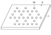
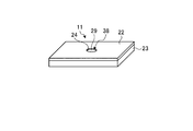
- FIG. 2 is a perspective view of a metal film-coated photonic crystal.
- FIG. 3 is a plan view of the metal film-coated photonic crystal.
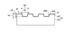
- FIG. 4 is a diagram showing a cross section along AA in FIG.
- FIG. 5 is a plan view of a metal film-coated photonic crystal of a comparative form.
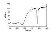
- FIG. 6 is a diagram illustrating the reflectance with respect to the wavelength of the reflected light in the example.
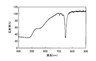
- FIG. 7 is a diagram illustrating the reflectance with respect to the wavelength of the reflected light in the comparative example.
- FIG. 8 is a diagram showing the sensitivity as a sensor for the examples and comparative examples.
- FIG. 9 is a view showing an AA cross section in FIG.
- FIG. 10 is a diagram illustrating a method for manufacturing a photonic crystal.
- FIG. 11 is a diagram illustrating a method for manufacturing a photonic crystal.
- FIG. 12 is a diagram illustrating a method for manufacturing a photonic crystal.
- FIG. 13 is a diagram for explaining the principle of the photonic crystal biosensor.
- FIG. 14 is a diagram for explaining the principle of a photonic crystal biosensor.
- FIG. 15 is a diagram for explaining the principle of the photonic crystal biosensor.
- FIG. 16 is a diagram for explaining the principle of the photonic crystal biosensor.
- FIG. 17 is a diagram illustrating a photonic crystal biosensor.
- FIG. 18 is a diagram illustrating a photonic crystal biosensor.
- FIG. 10 is a diagram illustrating a method for manufacturing a photonic crystal.
- FIG. 11 is a diagram illustrating a method for manufacturing a photonic crystal.
- FIG. 12 is a diagram illustrating a method for manufacturing a photonic crystal.
- FIG. 19 is a diagram illustrating a photonic crystal biosensor.
- FIG. 20 is a diagram for explaining the photonic crystal biosensor fixing means.
- FIG. 21 is a diagram for explaining the photonic crystal biosensor fixing means.
- FIG. 22 is a diagram illustrating another embodiment of the photonic crystal biosensor.
- FIG. 23 is a diagram illustrating an example in which the light detection unit of the target substance detection device irradiates light to the photonic crystal biosensor.
- FIG. 24 is a diagram illustrating a structure of a measurement probe included in the light detection unit of the target substance detection device.
- FIG. 25 is a diagram illustrating the evaluation conditions of the light detection unit of the target substance detection device.
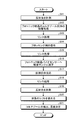
- FIG. 26 is a flowchart of the target substance detection method.
- FIG. 20 is a diagram for explaining the photonic crystal biosensor fixing means.
- FIG. 21 is a diagram for explaining the photonic crystal biosensor fixing means.
- FIG. 22 is a diagram illustrating another embodiment of the photonic crystal biosensor.
- FIG. 27 is a diagram for explaining the principle of the photonic crystal biosensor.
- FIG. 28 is a diagram for explaining the principle of a photonic crystal biosensor.
- FIG. 29 is a diagram for explaining the principle of the photonic crystal biosensor.
- FIG. 30 is a diagram illustrating the principle of the photonic crystal biosensor.
- FIG. 31 is a diagram for explaining the principle of the photonic crystal biosensor.
- FIG. 32 is a view showing a cross-sectional shape along the reflection surface of the non-flat portion
- FIG. 32 (a) is a view showing a non-flat portion having a regular hexagonal cross section
- FIG. 32 (b) is a cross-sectional view.
- FIG. 3 is a diagram showing a star-shaped non-flat portion.
- FIG. 3 is a diagram showing a star-shaped non-flat portion.
- FIG. 33 is a cross-sectional view of the metal film-coated photonic crystal according to the third embodiment, cut along a plane orthogonal to the reflecting surface.
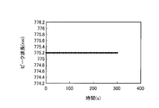
- FIG. 34 is a diagram illustrating a peak wavelength of a spectrum of reflected light when light is irradiated to the photonic crystal biosensor according to the first example.
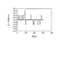
- FIG. 35 is a diagram illustrating a peak wavelength of a spectrum of reflected light when light is irradiated on the photonic crystal biosensor according to the first comparative example.
- FIG. 36 is a diagram showing the peak wavelength of the spectrum of reflected light when light is irradiated to the photonic crystal biosensor according to the second example.
- FIG. 37 is a diagram showing the peak wavelength of the spectrum of reflected light when light is irradiated to the photonic crystal biosensor according to the second comparative example.
- FIG. 1 is a diagram illustrating a target substance detection device.
- the target substance detection device 10 includes a photonic crystal biosensor (target substance capture device) 11, a light detection unit 12, and a processing unit 13 according to the first embodiment.
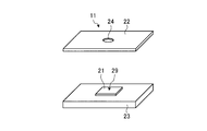
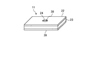
- the photonic crystal biosensor 11 includes a metal film-coated photonic crystal 21, an upper plate 22, and a lower plate 23.
- the upper plate 22 is provided with an opening 24.
- the photonic crystal biosensor 11 has a structure in which a metal film-covered photonic crystal 21 is sandwiched between an upper plate 22 and a lower plate 23.
- the photonic crystal biosensor 11 includes the upper plate 22 and the lower plate 23.
- the present invention is not limited to this, and the metal film-coated photonic crystal 21 is not limited thereto. It may be formed only by.
- FIG. 2 is a perspective view of the metal film-coated photonic crystal 21.
- FIG. 3 is a plan view of the metal film-covered photonic crystal 21.
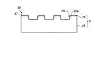
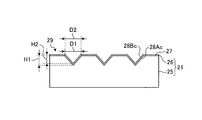
- FIG. 4 is a view showing a cross section taken along the line AA in FIG. 3, and shows a cross section when the photonic crystal 25 is cut along a plane orthogonal to the surface 27 of the photonic crystal 25.
- 2 to 4 are diagrams schematically showing the thickness, size, and the like of components constituting the metal film-coated photonic crystal 21. The same applies to the first embodiment and other embodiments described later.
- the metal film-covered photonic crystal 21 includes a photonic crystal 25 and a metal film 26.
- the metal film-covered photonic crystal 21 covers a reflective surface 29 in which a plurality of non-flat portions 28 ⁇ / b> A are arranged on the surface 27 of the photonic crystal 25 with a metal film 26.
- the non-flat portion 28 ⁇ / b> A is a cylindrical recess that is recessed with respect to the surface 27.
- a photonic crystal has a reflective surface in which concave portions having a predetermined depth or convex portions having a predetermined height are periodically formed on the surface, and light of a specific wavelength (parallel light) is irradiated onto the reflective surface. Then, it is a structure from which the reflected light can be obtained.
- a structure that obtains reflected light of a specific wavelength when light is irradiated onto a reflective surface having concave portions or convex portions formed periodically on the surface is generally called a photonic crystal.
- a photonic crystal is a structure having a lattice structure with sub-wavelength intervals. And when it irradiates the surface of a structure (henceforth a reflective surface) with the light of a wide region wavelength, it reflects or permeate
- the surface state of the photonic crystal depends on, for example, the shape and material of the photonic crystal. By reading the change in the reflected light or transmitted light, the change in the surface state of the photonic crystal can be quantified. Examples of changes in the surface state of the photonic crystal include adsorption of substances on the surface and structural changes.
- the amount of change in reflectance or transmittance at the extreme value (maximum value or minimum value) or the shift amount of the wavelength at which the reflectance or transmittance becomes an extreme value is obtained.
- the change in the surface state of the photonic crystal can be quantified by obtaining the amount of change with respect to the extreme value of interest or by obtaining the amount of shift of the wavelength that is the extreme value of interest.
- the photonic crystal 25 has a reflection surface 29 on the surface 27 of which a plurality of non-flat portions 28A are arranged.
- the reflection surface 29 is irradiated with light, light having a specific wavelength depending on the shape and material of the photonic crystal 25 is reflected.
- the arrangement in which the plurality of non-flat portions 28A are arranged is such that the center G1 of the non-flat portion 28A is located at the vertex position in the equilateral triangle Po in which the three non-flat portions 28A are three-fold symmetrical figures.
- a plurality of unit arrays U arranged so as to be stacked one by one are included.
- the plurality of unit arrays U are arranged so that the centroids G2 of the regular triangles Po overlap one by one at the position of the intersection of the lattice pattern La that is six-fold symmetric.
- sequence U is arrange
- the wavelength at which the reflected light of the light incident on the reflecting surface 29 of the photonic crystal 25 exhibits an extreme value depends on the period of the lattice pattern La on the reflecting surface 29.
- the period of the lattice pattern La is equal to the minimum distance B1 between the centroids G2. Therefore, in the first embodiment, the wavelength at which the reflected light of the light incident on the reflecting surface 29 exhibits an extreme value depends on the minimum distance B1 between the centroids G2.
- the unit array U includes a plurality of non-flat portions 28A
- the number of non-flat portions 28A on the entire reflecting surface is smaller than when the non-flat portions 28A are arranged to form the lattice pattern La. Become more.
- the distance C1 between the centers G1 of the non-flat portions 28A in the unit array U is not less than 0.4 times and not more than 0.6 times the minimum distance B1 between the centroids G2, which is equal to the minimum distance between intersections of the lattice pattern La. Is preferred.
- the reflective surface 29 can increase the number of non-flat portions 28A without reducing the period of the lattice pattern La, which is the minimum distance B1 between the centroids G2.
- the reflecting surface 29 increases the number of non-flat portions 28A per unit area while the diameter D1 of the non-flat portions 28A is maintained at a desired size.
- the photonic crystal 25 of 1st Embodiment can raise the sensitivity when it uses as a sensor because the specific surface area of the reflective surface 29 becomes large. Therefore, the sensor using the photonic crystal 25 of the first embodiment can increase the sensor sensitivity while setting the period of the lattice pattern La on the reflection surface 29 to a desired value.
- all the non-flat portions 28A belong to any unit array U.
- the non-flat portion 28A belonging to one unit array U is different from the non-flat portion 28A belonging to the adjacent unit array U.
- the non-flat portion 28A is not disposed at the position G3 in FIG. 3, for example.
- the position G3 is the position of the center of gravity of a triangle obtained by connecting the center of gravity G2 of three adjacent regular triangles Po with line segments.
- the non-flat portion 28A is not arranged alone, and thus the non-flat portion 28A does not form the lattice pattern La.
- the reflective surface 29 can increase the number of non-flat portions 28A without reducing the period of the lattice pattern La, which is the minimum distance B1 between the centroids G2. Therefore, the sensor using the photonic crystal 25 of the first embodiment can increase the sensor sensitivity while further reliably setting the cycle to a desired value.
- the distance C1 between the centers G1 is 0.5 times the minimum distance B1 between the centroids G2.
- the non-flat portions 28A are arranged at equal intervals in the direction of the lattice pattern La, so that the period of the lattice pattern La is hardly disturbed. For this reason, the half width of the spectrum shape of the reflected light is reduced, and noise in the measurement can be reduced. Therefore, the sensor using the photonic crystal 25 of the first embodiment has an improved S / N ratio and can further increase sensor sensitivity.
- the number of non-flat portions 28A included in the unit array U may not be three.
- the number of non-flat portions 28A included in the unit array U may be four or more.
- the position where the center G1 of the non-flat portion 28A overlaps in the unit array U may not be the vertex of the regular triangle Po.
- the position where the center G1 of the non-flat portion 28A overlaps in the unit array U may be the vertex of a figure that is rotationally symmetric other than an equilateral triangle.
- the position where the center of gravity G2 of the equilateral triangle Po overlaps may not be the intersection of the lattice pattern La that is 6-fold symmetric.
- the position where the center of gravity G2 of the regular triangle Po overlaps may be an intersection of lattice patterns that are rotationally symmetric other than 6-fold symmetry.
- a natural number of 2 or more is M
- a natural number of 2 or more is N
- a position where the center G1 of the non-flat portion 28A overlaps in the unit array U is a vertex of the M-fold symmetrical figure
- a center of gravity G2 of the regular triangle Po overlaps Is an intersection of lattice patterns that are N times symmetrical, M and N must be different.
- M is 3 and N is 6 as in the first embodiment shown in FIGS.
- the diameter D1 of the non-flat portion 28A is preferably 0.25 times or less the distance between the centers of gravity G2. Further, the diameter D1 of the non-flat portion 28A is preferably 50 nm or more and 1000 nm or less, and more preferably 100 nm or more and 500 nm or less. In addition, the shortest distance C1 between the centers G1 of the non-flat portion 28A is preferably 100 nm or more and 2000 nm or less, and more preferably 200 nm or more and 1000 nm or less.
- the aspect ratio (H1 / D1) of the non-flat portion 28A is preferably 0.1 or more and 10 or less, more preferably 0.5 or more and 5 or less. 0.0 or less.
- the dimension of the non-flat portion 28A is not limited to the above.
- an organic material such as a synthetic resin or an inorganic material such as a metal or ceramic can be used.
- Synthetic resins include polyethylene, polypropylene, polymethylpentene, polycycloolefin, polyamide, polyimide, acrylic, polymethacrylic acid ester, polycarbonate, polyacetal, polytetrafluoroethylene, polybutylene terephthalate, polyethylene terephthalate, polyvinyl chloride, polyvinyl chloride
- Thermosetting resins such as vinylidene, polystyrene, polyphenylene sulfide, polyether sulfone, and polyether ether ketone, and phenol resins, urea resins, and epoxy resins can be used.
- ceramics such as silica, alumina, zirconia, titania and yttria can be suitably used.
- metal various alloys including steel materials can be used. Specifically, stainless steel, titanium, a titanium alloy, or the like can be preferably used.
- Polycycloolefin synthetic resin or silica ceramic is more preferable. Among these, the polycycloolefin synthetic resin is most suitable because of its excellent processability.
- the photonic crystal 25 is produced by performing fine processing on the surface of the material substrate.
- a processing method laser processing, thermal nanoimprint, optical nanoimprint, a combination of a photomask and etching, or the like can be used.
- a thermoplastic resin such as a polycycloolefin-based synthetic resin
- a method using thermal nanoimprinting is preferable.
- the metal film 26 will be described.
- the reflective surface 29 of the photonic crystal 25 is covered with a metal film 26.
- the metal film 26 is preferably formed using at least one of gold (Au), silver (Ag), platinum (Pt), and aluminum (Al).
- the metal film 26 is made of Au.
- Au is preferable as the reflective surface 29 because it is excellent in stability.
- the surface is preferably covered with gold. By doing in this way, the usage-amount of gold
- the metal film-coated photonic crystal 21 is obtained by coating the reflective surface 29 of the photonic crystal 25 with the metal film 26, the metal film-coated photo is applied to the reflective surface 29 corresponding to the non-flat portion 28A of the photonic crystal 25.
- a non-flat portion 28B of the nick crystal 21 is formed.
- the diameter D2 of the non-flat part 28B is 0.25 times or less of the minimum distance B1 between the gravity centers G2.
- the diameter D2 of the non-flat portion 28B depends on the thickness of the metal film 26, it is preferably 50 nm or more and 1000 nm or less, and more preferably 100 nm or more and 500 nm or less.
- the shortest distance C2 between the centers G1 of the non-flat portion 28B is preferably 80 nm or more and 2400 nm or less, and more preferably 200 nm or more and 1000 nm or less. Further, when the depth of the non-flat portion 28B is H2, the aspect ratio (H2 / D2) of the non-flat portion 28B is preferably 0.1 or more and 10 or less, and more preferably 0.5 or more and 5 or less. 0.0 or less. The dimension of the non-flat portion 28B is not limited to the above.
- the thickness of the metal film 26 is small, part of the incident light on the photonic crystal 25 may pass through the metal film 26. As a result, a large amount of unnecessary information may be included in the reflected light from the photonic crystal 25, such as a reduction in the amount of information obtained from the reflected light, diffracted light, or reflected light from the back surface of the photonic crystal 25.
- unnecessary information contained in the reflected light from the photonic crystal 25 can be reduced, and the detection accuracy and concentration measurement accuracy of the target substance can be improved. Further, it is preferable that the thickness of the metal film 26 is moderately small because a detailed pattern shape can be easily formed on the surface 27 of the photonic crystal 25.
- the thickness of the metal film 26 is preferably 30 nm or more and 1000 nm or less, more preferably 150 nm or more and 500 nm or less, and further preferably 200 nm or more and 400 nm or less. This is because the change of the reflectance with respect to the wavelength becomes almost the same when the thickness of the metal film 26 exceeds 200 nm.
- the metal film 26 can be formed on the reflection surface 29 of the photonic crystal 25 by sputtering or vapor deposition.
- the outermost surface of the metal film 26 is preferably Au.
- Ag, Pt, and Al are used for the metal film 26, the wavelength of reflected light at each extreme value is 1.5 times that when Au is used as the metal film 26.
- Ag, Pt, and Al have a sensitivity that is 1.5 times that of Au. Since Ag is easily oxidized, it is preferable to form an oxide thin film such as Au or SiO 2 that is not easily oxidized after forming Ag on the reflective surface 29 of the photonic crystal 25. In this case, an Au film having a thickness of 5 nm can be formed on the surface of the Ag film having a thickness of 200 nm.
- the sensitivity is 1.5 times that of an Au film having a thickness of 200 nm. Further, no change in sensitivity was observed with or without the 5 nm Au film. Since Al is also easily oxidized like Ag, after forming an Al film on the surface 27 of the photonic crystal 25, it is preferable to form an oxide thin film such as Au or SiO 2 that is not easily oxidized. In order to modify with an antibody or the like, it is preferable that Pt also forms an oxide thin film such as Au or SiO 2 .
- the reflective surface 29 of the photonic crystal 25 is preferably modified using 3-triethoxysilylpropylamine (APTES) or the like.
- APTES 3-triethoxysilylpropylamine
- the Au or Ag metal film 26 is formed on the reflective surface 29 of the photonic crystal 25, it is not APTES but has a thiol group at one end and a functional group such as an amino group or a carboxyl group at the other end. It is preferable to modify the reflecting surface 29 of the photonic crystal 25 using the carbon chain that it has.
- a silane coupling agent having a functional group at one end for example, APTES is used to reflect the reflective surface of the photonic crystal 25. It is preferable to modify 29.
- the arrangement of the plurality of non-flat portions 28B arranged on the surface of the metal film-covered photonic crystal 21 is such that the three non-flat portions 28B are positioned at the vertices in the equilateral triangle Po.
- a plurality of unit arrays U arranged so as to overlap the centers G1 one by one are included.
- the arrangement in which the plurality of non-flat portions 28B are arranged is a plurality of unit arrays so that the centroids G2 of the equilateral triangle Po are overlapped one by one at the intersections of the lattice pattern La intersecting each other at an angle of 60 °.
- U is arranged.
- sequence U is arrange
- the wavelength at which the reflected light of the light incident on the reflective surface 29 of the metal film-coated photonic crystal 21 exhibits an extreme value depends on the period of the lattice pattern La on the reflective surface 29.
- the period of the lattice pattern La is equal to the minimum distance B1 between the centroids G2. Therefore, in the first embodiment, the wavelength at which the reflected light of the light incident on the reflecting surface 29 exhibits an extreme value depends on the minimum distance B1 between the centroids G2.
- the unit array U includes a plurality of non-flat portions 28B, the number of non-flat portions 28B on the entire reflecting surface is smaller than when the non-flat portions 28B are arranged so as to form the lattice pattern La. Become more. Further, the shortest distance between the centers G1 of the non-flat portion 28B and the length C1 of one side of the regular triangle Po in the unit array U is equal to the minimum distance B1 between the centroids G2 equal to the minimum distance between the intersections of the lattice pattern La. It is preferably 0.4 times or more and 0.6 times or less.
- the reflecting surface 29 can increase the number of non-flat portions 28B without reducing the period of the lattice pattern La, which is the minimum distance B1 between the centroids G2.
- the reflecting surface 29 increases the number of non-flat portions 28B per unit area while the diameter D2 of the non-flat portions 28B is maintained at a desired size.
- the metal film-covered photonic crystal 21 of the first embodiment can increase the sensitivity when used as a sensor by increasing the specific surface area of the reflecting surface 29. Therefore, the sensor using the metal film-covered photonic crystal 21 of the first embodiment can increase the sensor sensitivity while setting the period of the lattice pattern La on the reflection surface 29 to a desired value.
- all the non-flat portions 28B belong to any unit array U.
- the non-flat part 28B belonging to one unit array U is different from the non-flat part 28B belonging to the adjacent unit array U. Accordingly, the non-flat portion 28B is not disposed at the position G3 in FIG. 3, for example.
- the position G3 is the position of the center of gravity of a triangle obtained by connecting the center of gravity G2 of three adjacent regular triangles Po with line segments.
- the non-flat portion 28B is not disposed alone, and thus the non-flat portion 28B does not form the lattice pattern La.
- the reflective surface 29 can increase the number of non-flat portions 28B without reducing the period of the lattice pattern La, which is the minimum distance B1 between the centroids G2. Therefore, the sensor using the metal film-covered photonic crystal 21 of the first embodiment can increase the sensor sensitivity while further reliably setting the cycle to a desired value.
- the non-flat portion 28B By arranging the non-flat portion 28B in such an arrangement, the non-flat portion 28B is arranged on the reflecting surface 29 with only six rotational symmetries. Therefore, one large peak appears in the spectrum of reflected light, and the depth of the peak shape increases. As a result, a minute change on the reflection surface 29 can be detected with high accuracy, and noise in measurement can be further reduced. Therefore, the sensor using the metal film-covered photonic crystal 21 according to the first embodiment has an improved S / N ratio as compared with a plurality of rotationally symmetric arrangements, and can further increase sensor sensitivity.
- the diameter D2 of the non-flat portion 28B is preferably less than 1 time the length C1 of one side of the regular triangle Po. If D2 is 1 or more times C1, the adjacent non-flat portion 28B comes into contact with it, which is not preferable.
- the cross-sectional shape along the reflecting surface 29 of the non-flat portion 28B does not necessarily have to be a circle, and may be a regular hexagon as shown in FIG. 32 (a) or a star shape as shown in FIG. 32 (b). good.
- the shape of the non-flat portion 28B itself is also 6-fold symmetric. A peak appears, and sensor sensitivity can be improved.
- the circle includes a substantially circular shape.
- substantially circular means a circular shape whose shape is collapsed compared to a perfect circle but whose deviation from the perfect circle is within the range of processing errors. That is, the substantially circular shape means a circular shape that is not a perfect circle but is intended to be a perfect circle.
- the length of one side of the equilateral triangle Po is 0.5 times the minimum distance between the intersections of the lattice pattern La, and one side of the equilateral triangle Po is preferably parallel to the straight line included in the lattice pattern La. Since the non-flat portions 28A are arranged at equal intervals in the direction of the lattice pattern La, the period of the lattice pattern La is hardly disturbed. For this reason, the half width of the spectrum shape of the reflected light is reduced, and noise in the measurement can be reduced. Therefore, the sensor using the photonic crystal 25 of the first embodiment has an improved S / N ratio and can further increase sensor sensitivity.
- FIG. 5 is a plan view of a metal film-coated photonic crystal 21 of a comparative form.
- the array in which the plurality of non-flat portions 28A and 28B are arranged is arranged such that the centers G1 overlap one by one at the intersection point of the lattice pattern La that is six-fold symmetric.
- the distance between the centers G1 in the comparative embodiment is equal to the minimum distance B1 between the centroids G2 in the first embodiment.
- the results obtained by measuring the wavelength spectrum using the metal film-coated photonic crystal 21 of the first embodiment shown in FIGS. 2 to 4 are taken as examples. Moreover, let the result of having measured a wavelength spectrum using the metal film covering photonic crystal 21 of the comparative form shown in FIG. 5 be a comparative example.
- the examples and comparative examples are results when the diameter D2 of the non-flat portion 28B is 200 nm and the minimum distance B1 between the centroids G2 is 600 nm.
- FIG. 6 is a diagram illustrating the reflectance with respect to the wavelength of the reflected light in the example.
- FIG. 7 is a diagram illustrating the reflectance with respect to the wavelength of the reflected light in the comparative example. 6 and 7, it can be seen that the example and the comparative example show the wavelength at which the reflectance shows an extreme value due to the minimum distance B1 between the centroids G2 being 600 nm.
- FIG. 8 is a diagram showing the sensitivity as a sensor for the examples and comparative examples.
- FIG. 8 shows the sensitivity as a sensor obtained from the shift amount of the extreme wavelength when biotin is immobilized on the surface 27 of the reflecting surface 29 and 100 nm of avidin is reacted, with respect to Examples and Comparative Examples.
- FIG. 8 shows that the sensitivity of the example is higher than that of the comparative example. This is because the number of non-flat portions 28A and 28B per unit area is greater than that of the comparative example even though the period of the lattice pattern La on the reflecting surface 29 is the same as the minimum distance B1 between the centroids G2. This is because there are many.
- the non-flat portion according to the first embodiment is a concave portion as shown in FIG. 4, but may be a convex portion as shown in FIG.
- the non-flat portions 28 ⁇ / b> A and 28 ⁇ / b> B are cylindrical convex portions that protrude from the surface 27.
- FIG. 9 is a view showing an AA cross section in FIG. 3 when the non-flat portion is a convex portion.
- FIG. 11 and FIG. 12 are diagrams for explaining a photonic crystal manufacturing method.
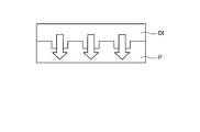
- a mold DI having a pattern of a nanometer-level fine structure or a nanometer-level periodic structure is used.
- the heated mold DI is pressed against the sheet-shaped resin P, pressed at a predetermined pressure for a predetermined time, and released when the surface temperature of the mold DI reaches a predetermined temperature.
- the structure and the periodic structure are transferred to the sheet-like resin P. Thereby, the photonic crystal 25 is obtained.
- the mold DI is heated to about 160 ° C., pressed at a pressure of about 12 MPa for a predetermined time, and released when the surface temperature of the mold DI reaches about 60 ° C. It is preferable.
- a metal film 26 is formed on the surface in contact with the mold DI by a sputtering or vapor deposition apparatus or the like, and the metal film-covered photonic crystal 21 is completed. .
- the target substance is an object to be detected by the target substance detection apparatus 10 and may be any of a polymer such as a protein, an oligomer, and a low molecule.
- the target substance is not limited to a single molecule, and may be a complex composed of a plurality of molecules.
- Examples of the target substance include pollutants in the atmosphere, harmful substances in water, biomarkers in the human body, and the like. Of these, cortisol and the like are preferable.
- Cortisol is a low molecular weight substance with a molecular weight of 362 g / mol.
- Cortisol is attracting attention as a substance that evaluates the degree of stress felt by humans because cortisol concentration in saliva increases when humans feel stress.
- concentration of cortisol as a target substance, for example, the degree of stress can be evaluated by measuring the concentration of cortisol contained in human saliva. If the degree of stress is evaluated, it can be determined whether or not the subject is in a stress state at a level that leads to mental illness such as depression.
- the target substance capturing substance is a substance that binds to the target substance and captures the target substance.
- the term “bonded” refers to a bond that is not chemically bonded, such as a bond by chemical adsorption or van der Waals force, in addition to the case of chemically bonding.
- the target substance capturing substance is a substance that specifically reacts with the target substance to capture the target substance, and is preferably an antibody having the target substance as an antigen.
- Specific reaction means selectively forming a complex by reversibly or irreversibly binding to a target substance, and is not limited to a chemical reaction.
- a substance that reacts specifically may exist in addition to the target substance.
- the target substance can be quantified if the affinity is very small compared to the target substance.
- an antibody using the target substance as an antigen an artificially prepared antibody, a molecule composed of a substance constituting DNA such as adenine, thymine, guanine, and cytosine, a peptide, and the like can be used.
- the target substance capturing substance is preferably a cortisol antibody.
- a known method can be employed to produce the target substance capturing substance.
- the antibody can be produced by a serum method, a hybridoma method, or a phage display method.
- Molecules composed of substances constituting DNA can be produced by, for example, the SELEX method (Systematic Evolution of Ligands by Exponential Enrichment).
- the peptide can be prepared by, for example, a phage display method.
- the target substance capturing substance does not need to be labeled with any enzyme / isotope. However, it may be labeled with an enzyme / isotope.
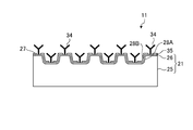
- the target substance capturing substance is fixed to the reflection surface 29 of the metal film-coated photonic crystal 21 shown in FIG.
- means for fixing the target substance capturing substance to the reflecting surface 29 of the metal film-coated photonic crystal 21 include chemical bonds such as covalent bonding, chemical adsorption, and physical adsorption, and physical bonding methods. These means can be appropriately selected according to the properties of the target substance-capturing substance. For example, when adsorption is selected as the fixing means, the adsorption operation is as follows.
- a solution containing a target substance-capturing substance is dropped on the reflective surface 29 of the metal film-coated photonic crystal 21, and the metal film-coated photonic crystal 21 is cooled at a predetermined time, at room temperature, or as necessary. Heating causes the target substance capturing substance to be adsorbed on the reflecting surface 29.
- the photonic crystal biosensor 11 previously adsorbs (fixes) an antibody (for example, cortisol antibody) that binds only to a specific antigen (for example, cortisol) on the surface of the reflective surface 29 of the metal film-coated photonic crystal 21. Thereby, the photonic crystal biosensor 11 can detect a specific antigen.
- an antibody for example, cortisol antibody
- a specific antigen for example, cortisol
- the photonic crystal biosensor 11 may be one in which a blocking agent (protective substance) is immobilized on a reflective surface 29 on which an antibody that is a target substance capturing substance is immobilized.
- the blocking agent is immobilized before the target substance is brought into contact with the photonic crystal biosensor 11.
- the surface of the reflecting surface 29 of the photonic crystal 25 is generally superhydrophobic. For this reason, impurities other than the antibody that is the target substance-capturing substance may be adsorbed on the reflecting surface 29 due to the hydrophobic interaction.
- the optical characteristics of the photonic crystal 25 are greatly influenced by the surface state, it is preferable that no impurities are adsorbed on the reflection surface 29 of the photonic crystal 25. Since the blocking agent is fixed to the reflection surface 29 of the photonic crystal 25, the detection accuracy of the reflected light can be improved.
- a so-called blocking agent is fixed in advance so that impurities and the like are not fixed to a portion other than the portion where the antibody that is the target substance capturing substance is adsorbed (fixed) to the reflection surface 29 of the photonic crystal 25.
- the blocking agent is brought into contact with the surface of the photonic crystal 25.
- the blocking agent skim milk, bovine serum albumin (BSA), or the like can be used.
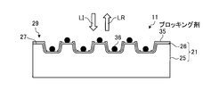
- FIGS. 13 to 16 are diagrams for explaining the principle of the photonic crystal biosensor 11.
- the photonic crystal biosensor 11 has optical characteristics of the photonic crystal 25 and various biological / chemical reactions that occur on or near the surface of the photonic crystal 25, for example, a specific antigen is only a specific antibody. By utilizing the antigen-antibody reaction of reacting, a minute amount of protein or low molecular weight substance is detected.
- the photonic crystal biosensor 11 reflects the wavelength of the reflected light due to the surface plasmon resonance phenomenon and / or the localized surface plasmon resonance phenomenon when the reflection surface 29 of the metal film-coated photonic crystal 21 is irradiated with light of a specific wavelength. Use the phenomenon of extreme values shifting.
- an antibody (target substance-capturing substance) 34 is fixed to the surface of the reflection surface 29 of the metal film-coated photonic crystal 21 by adsorption.
- a blocking agent (protective substance) 35 is preliminarily adsorbed on a portion of the reflective surface 29 other than the portion where the antibody 34 is adsorbed, that is, the reflective surface 29 other than the portion where the antibody 34 is adsorbed. . This prevents impurities or the like from being adsorbed on the reflective surface 29 other than the portion where the antibody 34 is adsorbed.
- an antigen (target substance) 36 is brought into contact with the photonic crystal biosensor 11 on which the antibody 34 and the blocking agent 35 are adsorbed, and an antigen-antibody reaction is performed.
- a complex 37 in which the antigen 36 is captured by the antibody 34 is fixed to the reflecting surface 29.
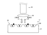
- the light detection unit 12 illustrated in FIG. 1 converts the light (incident light) LI having a specific wavelength into parallel light in a state where the antigen 36 is captured by the reflection surface 29 of the photonic crystal 25. Then, the reflective surface 29 of the metal film-coated photonic crystal 21 is irradiated.
- the light detection unit 12 illustrated in FIG. 1 detects the reflected light LR reflected by the reflecting surface 29 and obtains the wavelength of the extreme value of the reflected light LR.
- the processing unit 13 illustrated in FIG. 1 obtains the wavelength at the extreme value of the intensity of the reflected light LR and the shift amount of the wavelength at the extreme value of the intensity, and is captured by the reflective surface 29 of the metal film-covered photonic crystal 21. The presence or absence of the antigen 36 is detected, or the concentration of the antigen 36 is obtained.
- the photonic crystal biosensor 11 can change the types of various biological substances such as proteins or low molecular weight substances, such as proteins, which are detection target substances, by changing the type of combination of the antibody 34 and the antigen 36. .
- the photonic crystal biosensor 11 when the antigen 36 is captured by the antibody 34 fixed to the reflecting surface 29, the state of the reflecting surface 29 changes, and the reflected light LR changes.
- the photonic crystal biosensor 11 outputs an optical physical quantity.
- This physical quantity correlates with a change in the surface state of the reflective surface 29 of the metal film-coated photonic crystal 21, and correlates with the amount of the complex 37 formed by capturing the antigen 36 on the antibody 34 immobilized on the reflective surface 29.
- the optical physical quantity is, for example, the shift amount of the wavelength at which the intensity of the reflected light LR is an extreme value, the change amount of the reflectance of the light, the shift amount of the wavelength at which the reflectance of the light is an extreme value, the intensity of the reflected light LR. And the amount of change in the extreme value of the intensity of the reflected light LR.
- the shift amount of the wavelength at which the intensity of the reflected light LR or the reflectance of the light becomes an extreme value is used.
- the target substance detection device 10 shown in FIG. 1 can be made compact.
- FIG. 17 is explanatory diagrams of the photonic crystal biosensor 11.
- the upper plate 22 is placed on the lower plate 23 as shown in FIG.
- the photonic crystal biosensor 11 is produced by sandwiching 21 between the lower plate 23 and the upper plate 22.
- the end of the opening 24 on the lower plate 23 side is closed by the reflection surface 29 of the photonic crystal 25.
- the upper plate 22 has a droplet holding portion 38 having a constant volume, which is formed by being surrounded by the inner wall on the opening 24 side and the reflecting surface 29.
- the inner wall on the opening 24 side refers to the inner wall of the upper plate 22 that is a boundary surface between the upper plate 22 and the opening 24.
- FIG. 19 shows a state in which a predetermined solution is dropped on the droplet holder 38.
- the droplet holding part 38 exhibits the droplet holding function, the solution is prevented from flowing out from the opening 24.
- the target substance can be sufficiently detected and measured.
- the shape of the opening 24 is not limited to a cylindrical shape, and may be any other shape as long as a droplet can be held inside the opening 24.
- its diameter may be varied depending on the type of combination of the antibody 34 and the antigen 36, the required measurement accuracy, or the optical system of the reflected light detector. it can.
- the diameter of the opening 24 is preferably 0.5 mm to 10 mm, more preferably 2 mm to 6 mm in consideration of the operation and the convenience of handling when the antigen 34 is adsorbed to the antibody 34 described above. .
- the material of the upper plate 22 and the lower plate 23 is not particularly limited. However, in consideration of the cleanliness of the surfaces of the upper plate 22 and the lower plate 23, it is preferable to use stainless steel, polycycloolefin resin, silica, or the like.
- the upper plate 22 may be formed of a hydrophobic material.
- a so-called hydrophilic solution such as saliva
- the upper plate 22 is made of a hydrophobic material
- the solution can be accurately collected in the droplet holder 38.
- detecting and measuring a so-called lipophilic solution such as lipid
- the solution can be accurately collected in the droplet holding unit 38 if the upper plate 22 is formed of a hydrophobic material.
- the upper plate 22 may be formed of a material having water repellency, oil repellency or water / oil repellency. Further, a surface treatment or coating that exhibits hydrophobicity, hydrophilicity, water repellency, and oil repellency may be applied to the upper plate 22. By doing so, the solution can be accurately collected in the droplet holder 38.
- the photonic crystal biosensor 11 fixes the photonic crystal biosensor 11 by determining the position of the photonic crystal biosensor 11 with respect to the light detection unit 12 shown in FIG. 1 below the photonic crystal biosensor 11. It is preferable to attach a fixing material (target substance capturing part fixing means, photonic crystal biosensor fixing means) for this purpose.
- a fixing material target substance capturing part fixing means, photonic crystal biosensor fixing means
- a magnet sheet, a double-sided tape, an adhesive, or the like can be used.
- a vacuum chuck or an electrostatic chuck may be used as a fixing mechanism instead of a fixing material.
- 20 and 21 are diagrams for explaining the photonic crystal biosensor fixing means.
- 20 shows a state before the magnet sheet 39 is attached
- FIG. 21 shows a state after the magnet sheet 39 is attached.
- the photonic crystal biosensor 11 has a magnet sheet 39 attached to the lower side of the photonic crystal biosensor 11.
- the magnet sheet 39 functions as a photonic crystal biosensor fixing means.
- the photonic crystal biosensor 11 is uniformly produced by thermal nanoimprint or the like. In order for the target substance detection apparatus 10 to detect reflected light more accurately, it is preferable to accurately position the incident site and the reflected site of the light irradiated to the photonic crystal biosensor 11.
- the positional relationship at the time of measurement between the photonic crystal biosensor 11 and a measurement probe described later is preferably the same before and after the antigen-antibody reaction, and the same portion is preferably measured. Therefore, the distance between the measurement probe and the reflection surface 29 of the photonic crystal biosensor 11 is preferably the same before and after the antigen-antibody reaction, and is preferably fixed to 50 ⁇ m to 500 ⁇ m. Since the photonic crystal biosensor 11 includes the upper plate 22, the upper plate 22 functions as a spacer, and the distance between the measurement probe and the reflection surface 29 of the photonic crystal biosensor 11 can be made constant.
- the photonic crystal biosensor 11 may be marked with a positioning marker that displays a specific position on the reflecting surface 29.
- the marker can be attached by photolithography, sputtering, vapor deposition, a lift-off process using these, printing with ink or the like, or pattern formation by imprinting.
- the marker may be attached to either the front surface (the reflective surface 29 side) or the back surface (the opposite side of the reflective surface 29) of the photonic crystal biosensor 11 as long as the position can be read.
- the measurement part of the photonic crystal 25 may be removed and a marker may be attached to the photonic crystal 25 itself. Further, a marker may be attached to the upper plate 22 and the lower plate 23.
- FIG. 22 is a diagram for explaining another form of the photonic crystal biosensor 11.
- the photonic crystal biosensor 11 includes a member that closes the opening 24.
- the member that closes the opening 24 includes a cover 41 with a hole and a sheet 42.
- the cover 41 with a hole is a plate-like member having an opening 43, and the cover 41 with a hole is provided on the surface (the reflection surface 29 side) of the photonic crystal biosensor 11.
- the sheet 42 is provided on the opposite side (light incident side) of the cover 41 with holes from the photonic crystal biosensor 11.
- the sheet 42 functions as a covering member.
- the openings 24 and 43 are closed by the cover 41 with a hole and the sheet 42.
- the space surrounded by the inner wall on the opening 43 side of the cover 41 with the hole, the inner wall on the opening 24 side, and the reflection surface 29 of the photonic crystal 25 is a droplet holding unit 44 having a constant volume.
- the inner wall on the opening 43 side refers to the inner wall of the holed cover 41 that is a boundary surface between the holed cover 41 and the opening 43.
- the opening 43 is covered with the sheet 42 after the target substance is disposed in the droplet holding unit 44. As a result, the droplet holder 44 is blocked by the sheet 42.
- the photonic crystal biosensor 11 includes the holed cover 41 and the sheet 42, thereby suppressing evaporation of the solution dropped on the opening 24 of the photonic crystal biosensor 11. For this reason, it can suppress that the density
- the sheet 42 is preferably a transparent material, and more preferably a sheet that absorbs light having a wavelength at the extreme value of the intensity of reflected light.
- the material of the sheet 42 is preferably quartz (silica) or the like when measured with reflected light from the visible light region to the ultraviolet region.
- the light detection unit 12 illustrated in FIG. 1 includes a light source 51, a measurement probe 52, a light detection device 53, a first optical fiber 54, a second optical fiber 55, and a collimator lens 56.
- the light source 51 and the measurement probe 52 are optically connected by a first optical fiber 54.
- the measurement probe 52 and the light detection device 53 are optically connected by a second optical fiber 55.
- a control device that is connected to the light source 51 and the light detection device 53 and that controls the light source 51 and processes a signal from the light detection device 53 may be provided.
- FIG. 23 is a diagram illustrating an example in which the light detection unit 12 irradiates the photonic crystal biosensor 11 with light.
- the first optical fiber 54 shown in FIG. 1 guides the light from the light source 51 shown in FIG. 1 to the measurement probe 52, and from the measurement probe 52 to the reflection surface 29 of the metal film-coated photonic crystal 21 included in the photonic crystal biosensor 11. Irradiate.
- the collimating lens 56 irradiates the reflecting surface 29 of the photonic crystal 25 as incident light LI after collimating the light emitted from the first optical fiber 54 and irradiated from the measurement probe 52.
- the second optical fiber 55 receives the light reflected by the reflection surface 29 of the metal film-covered photonic crystal 21 as reflected light LR, and guides it to the light detection device 53 shown in FIG.
- the kind of collimating lens 56 is not specifically limited,
- the antireflection film which has a nanostructure can be used.
- the light detection device 53 is a device for detecting light including a light receiving element such as a phototransistor or a CCD (Charge Coupled Device).
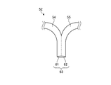
- FIG. 24 is a diagram showing the structure of the measurement probe 52 included in the light detection unit 12 shown in FIG.
- the first optical fiber 54 and the second optical fiber 55 are joined.
- the light exit surface 61 of the first optical fiber 54 and the incident surface 62 of the reflected light LR of the second optical fiber 55 are disposed on the same surface (incident / exit surface) 63.
- the measurement probe 52 includes the first optical fiber 54 and the second optical fiber 55 on the emission side (emission surface 61 side) of the first optical fiber 54 and the incident side (incident surface 62 side) of the second optical fiber 55. It is united. Then, the measurement probe 52 enters light using the first optical fiber 54 and the second optical fiber 55 and detects the reflected light LR.
- the measurement probe 52 Since the measurement probe 52 has such a structure, the incident light LI irradiated to the reflection surface 29 of the photonic crystal 25 and the reflection light LR from the reflection surface 29 are emitted from substantially the same position and are incident. Can do. While the measurement probe 52 is configured as described above, and the collimator lens 56 is used to convert the light from the measurement probe 52 into parallel light, the light detection unit 12 converts the incident light LI of parallel light onto the reflection surface 29. It can be incident vertically. At the same time, the reflected light LR reflected perpendicularly from the reflecting surface 29 can be received. By doing in this way, the measurement probe 52 can suppress the fall of reflected light intensity to the minimum, and can mainly detect the 0th-order light component of the reflected light LR.
- the method for detecting the reflected light LR is not limited to the measurement probe 52 as described above.
- a half mirror may be disposed between the collimating lens 56 and the reflection surface 29, and the reflected light LR may be separated by the half mirror and guided from the second optical fiber 55 to the light detection device 53.
- FIG. 25 is a diagram illustrating evaluation conditions of the light detection unit 12 of the target substance detection device 10 according to the first embodiment.
- the light detection unit 12 arranges a collimator lens 56 between the incident / exit surface 63 of the measurement probe 52 and the reflection surface 29 of the metal film-covered photonic crystal 21.
- the distance (measurement distance) between the collimating lens 56 and the reflecting surface 29 is h
- the diameter of the parallel light emitted from the collimating lens 56 is d1
- the diameter of the opening 24 through which the reflecting surface 29 of the photonic crystal 25 is exposed Is d2.
- h was 15 mm or 40 mm
- d1 was 3.5 mm
- d2 was 5 mm.
- the optical axis ZL of the light applied to the reflecting surface 29 and the optical axis ZL of the reflected light reflected by the reflecting surface 29 are both orthogonal to the reflecting surface 29.
- the diameter of the measurement probe 52 is 200 ⁇ m.
- White light was used as the irradiation light.
- the reflectance is the ratio of the standard material (aluminum plate) to the reflected light intensity.
- the processing unit 13 obtains the extreme wavelength of the reflected light detected by the light detection unit 12. At the same time, the processing unit 13 detects at least the presence / absence of the target substance (for example, the antigen 36 shown in FIGS. 15, 16, and the like) based on the obtained extreme wavelength shift (wavelength shift amount).
- the processing unit 13 is, for example, a microcomputer. There is a correlation between the amount of wavelength shift and the concentration of the target substance trapped on the reflection surface 29 of the metal film-coated photonic crystal 21. For this reason, the processing unit 13 can obtain the concentration of the target substance captured by the reflection surface 29 from the wavelength shift amount.
- a method for detecting a target substance using the target substance detection apparatus 10 shown in FIG. 1 will be described.
- a case will be described in which cortisol antibody is adsorbed on the reflective surface 29 of the metal film-coated photonic crystal 21 and cortisol in saliva is detected and measured as a target substance to be detected.
- the photonic crystal 25 a cycloolefin polymer sheet having a predetermined fine structure formed on the surface by thermal nanoimprint is cut into a predetermined size.
- FIG. 26 is a flowchart showing an example of the target substance detection method according to the first embodiment.
- the light detection unit 12 detects the reflected light LR from the reflection surface 29 when the reflection surface 29 of the photonic crystal 25 is irradiated with light, and the processing unit 13 measures the reflected light LR.
- the processing unit 13 measures the spectrum of the reflected light intensity of the reflected light LR.
- the wavelength of the light (incident light LI) applied to the reflecting surface 29 is, for example, not less than 300 nm and not more than 2000 nm.
- step S 12 a cortisol antibody solution (cortisol antibody concentration of 1 ⁇ g / ml to 50 ⁇ g / ml) is dropped onto the reflective surface 29 of the metal film-coated photonic crystal 21. Then, the photonic crystal biosensor 11 is allowed to stand at a predetermined temperature for a predetermined time for a predetermined time or if necessary, and the cortisol antibody is adsorbed on the reflection surface 29 of the metal film-coated photonic crystal 21.
- cortisol antibody concentration 1 ⁇ g / ml to 50 ⁇ g / ml
- step S13 a phosphate buffer solution (PBS: Phosphate buffered saline) is dropped onto the reflective surface 29 of the metal film-coated photonic crystal 21. Thereafter, a rinsing process is performed a plurality of times for removal by centrifugal force or the like.
- PBS Phosphate buffered saline
- step S14 skim milk is dropped as the blocking agent 35 onto the reflecting surface 29 of the photonic crystal 25, and the photonic crystal biosensor 11 is left for a predetermined time at a predetermined time or a predetermined temperature if necessary.
- the skim milk is adsorbed to the non-adsorbing portion of the cortisol antibody on the reflection surface 29 of the metal film-coated photonic crystal 21.
- step S15 the rinsing process is performed a plurality of times with a phosphate buffer solution in the same manner as the rinsing process (step S13).
- a predetermined treatment is performed on the reflection surface 29 of the metal film-coated photonic crystal 21, and the photonic crystal biosensor 11 is formed.
- saliva is first prepared as a solution containing cortisol.
- Pretreatment such as saliva sampling and impurity removal is performed using, for example, a commercially available saliva collection kit.
- the preparation of saliva may be performed at any time before the saliva is dripped onto the photonic crystal biosensor 11. For example, it may be performed before the photonic crystal biosensor 11 is formed, may be performed in parallel with the formation of the photonic crystal biosensor 11, or may be performed after measuring the reflected light intensity. 10 ⁇ L to 50 ⁇ L of saliva after sampling and pretreatment is dropped onto the photonic crystal biosensor 11.
- step S17 the photonic crystal biosensor 11 is allowed to stand for a predetermined time at a predetermined temperature for a predetermined time or, if necessary, for an antigen-antibody reaction.
- step S18 the rinsing process is performed a plurality of times with a phosphate buffer solution in the same manner as the rinsing process (step S15).
- step S19 the target substance detection device 10 is used to irradiate the reflection surface 29 of the metal film-coated photonic crystal 21 with light.
- the light irradiated at this time is the same as the light irradiated on the reflecting surface 29 in step S11.
- the target substance detection device 10 measures the reflected light LR from the reflecting surface 29, for example, the spectrum of the reflected light intensity.
- the wavelength at the extreme value of the reflected light intensity of the photonic crystal biosensor 11 changes due to the influence of an antigen-antibody reaction or the like in the vicinity of the reflecting surface 29 or the reflecting surface 29. For this reason, cortisol in saliva can be detected from the difference in wavelength at the extreme value of reflected light intensity before and after the reaction, that is, the amount of wavelength shift. Further, the concentration of cortisol in saliva can be obtained from the wavelength shift amount.
- step S20 the processing unit 13 obtains the wavelength shift (wavelength shift amount) at the extreme value (minimum value) of the reflected light intensity (or reflectance) measured in step S19.
- the wavelength shift amount is, for example, the extreme value (minimum value) of the wavelength ⁇ 2 after the target material is captured on the reflective surface 29 and the reflected light intensity (or reflectance) when the target material is not captured on the reflective surface 29. ) Is the difference ⁇ 2 ⁇ 1 with respect to the wavelength ⁇ 1.
- step S21 the processing unit 13 determines that cortisol is present in saliva when there is a wavelength shift amount of a predetermined amount or more.
- the processing unit 13 determines the concentration of cortisol based on the amount of wavelength shift using, for example, a relational expression between the amount of wavelength shift and the concentration of cortisol. At this time, the relational expression is obtained in advance and stored in the storage unit of the processing unit 13.
- the wavelength shift amount is obtained using the extreme wavelength of the reflected light intensity on the reflection surface 29 in a state where the target substance is not captured, but the present invention is not limited to this.
- the wavelength shift amount may be obtained using the extreme wavelength of the intensity of the reflected light from the reflecting surface 29 after the rinsing process (step S13 or step S15) is finished. Further, when there are a plurality of extreme values in step S11 and step S19, the extreme value to be noted is appropriately selected. Then, the wavelength ⁇ 1 and the wavelength ⁇ 2 are obtained for the selected extreme value.
- the metal film-covered photonic crystal 21 has the antibody 34 immobilized on the reflection surface 29.
- the antibody 34 may be used without being fixed to the surface 29.
- a target substance detection apparatus provided with a target substance capturing apparatus according to a second embodiment will be described.
- the substance (target substance) 36 that is fixed to the reflecting surface 29 of the metal film-coated photonic crystal 21 is used as an antigen (target substance) 36, and the antibody 34 is adsorbed to the antigen 36.
- the second embodiment is the same as the first embodiment, and a duplicate description is omitted.
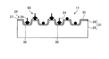
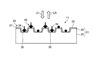
- FIGS. 27 to 31 are diagrams for explaining the principle of the photonic crystal biosensor.
- the specific reaction between the antibody 34 and the antigen 36 will be described using cortisol as the antigen 36 and an anti-cortisol antibody as the antibody 34.
- the photonic crystal biosensor 11 is similar to the means for fixing the antibody 34 to the reflection surface 29 as means for fixing the antigen 36 to the reflection surface 29 of the metal film-coated photonic crystal 21. It can be carried out.
- means for fixing the antigen 36 to the reflecting surface 29 include chemical bonding and physical bonding methods such as covalent bonding, chemical adsorption, and physical adsorption. These means can be appropriately selected according to the properties of the antigen 36.
- the amount of the antigen 36 immobilized on the metal film-coated photonic crystal 21 is a fixed amount.
- the antibody 34 is adsorbed to the antigen 36 fixed to the metal film-coated photonic crystal 21 to form a complex 65 (see FIGS. 29 and 30)
- the photonic crystal biosensor 11 can output the correlated physical quantity.
- the fixed amount of the antigen 36 to be fixed may be appropriately changed. For example, it can be set to an optimum amount according to the range of the amount of the antigen 36 contained in the sample S.
- the blocking agent 35 is fixed to a portion of the reflecting surface 29 where the antigen 36 is not attached.
- the reflective surface 29 of the photonic crystal 25 is irradiated with light (incident light) LI of, for example, 300 nm or more and 900 nm or less as parallel light so that the optical axis is orthogonal to the reflective surface 29.
- a wavelength at which the intensity or reflectance of the reflected light LR at this time becomes an extreme value (minimum value in this example) is ⁇ 1.
- a mixture 65 containing the complex 65 of the antigen 36 and the antibody 34 and the antibody 34 is prepared.
- the mixture M is obtained by mixing the sample S containing the antigen 36 and a solution containing a known amount of the antibody 34.
- the complex 65 is obtained by reacting the antibody 34 and the antigen 36 by mixing the sample S containing the antigen 36 and a solution containing a known amount of the antibody 34.
- the antibody 34 remains in the mixture M without reacting with the antigen 36 by increasing the known amount of the antibody 34 to the amount of the site to which the antigen 36 is contained in the sample S.
- the mixture M is brought into contact with the reflection surface 29 of the metal film-coated photonic crystal 21. Thereby, as shown in FIG.
- a complex 65 is formed on the reflective surface 29 by the antigen 36 and the antibody 34 fixed on the reflective surface 29.
- light (incident light) LI of, for example, 300 nm or more and 2000 nm or less is parallel light and the optical axis is orthogonal to the reflection surface 29 on the reflection surface 29 of the metal film-covered photonic crystal 21. Irradiate.
- the wavelength at which the reflected light intensity or reflectance of the reflected light LR becomes an extreme value (a minimum value in this example) is ⁇ 2.
- the wavelength shift amount of the wavelength at which the light reflectance is an extreme value is ⁇ 2 ⁇ 1.
- the amount of wavelength shift changes according to the change in the surface state of the reflection surface 29 of the metal film-coated photonic crystal 21.
- the antigen 36 is detected and quantified.
- the photonic crystal biosensor 11 outputs an optical physical quantity. This physical quantity correlates with a change in the surface state on the reflecting surface 29 and correlates with the amount of the complex 65 formed by the antigen 36 and the antibody 34 immobilized on the reflecting surface 29.
- cortisol which is an antigen 36
- an anti-cortisol antibody which is an antibody 34
- the second embodiment is compared with the case of the second embodiment.
- X be the amount of the site to which antigen 36 is bound in sample S
- C be the known amount of antibody 34 in mixture M.
- the relationship between X and C is such that X is less than C (X ⁇ C).
- the antigen 36 and the antibody 34 undergo an antigen-antibody reaction to form a complex 65. Since X is less than C (X ⁇ C), the amount of antibody 34 in mixture M is CX.
- the antibody 34 in the mixture M reacts with the antigen 36 on the reflecting surface 29 to form a complex 65.
- the amount of antigen 36 immobilized on the reflecting surface 29 is equal to or greater than the amount CX of the antibody 34 in the mixture M.
- the amount of the complex 65 becomes CX.
- the relationship between the amount of the composite 65 fixed to the reflecting surface 29 and the wavelength shift amount ⁇ is obtained in advance. From the above relational expression, the amount X of the antigen 36 can be determined by C ⁇ / k. The concentration of the antigen 36 can be determined based on the amount X of the antigen 36.
- the photonic crystal biosensor 11 uses, for example, a secondary antibody that specifically reacts with the complex 65 as a complex binding substance, and the reflective surface 29 of the metal film-coated photonic crystal 21. You may make it react with the composite_body
- the secondary antibody is brought into contact with the reflecting surface 29 of the metal film-covered photonic crystal 21 in an excessive amount than the first complex 65.
- a secondary antibody is added to all the complexes 65 to form a second complex. By doing so, the change in the surface state of the metal film-coated photonic crystal 21 is further increased.
- the sensitivity of the photonic crystal biosensor 11 further increases.
- the secondary antibody may be used as it is, or may be used after adding other substances. Since the change in the surface state of the metal film-coated photonic crystal 21 increases as the secondary antibody increases, the photonic crystal biosensor 11 can be reacted with the complex 65 after adding another substance to the secondary antibody. The sensitivity is further increased.
- the reflective surface 29 after the second composite is formed is irradiated with light.
- the wavelength at which the reflected light intensity or reflectance obtained as a result is an extreme value (minimum value in this example) is ⁇ 2.
- the extreme value of interest is appropriately selected.
- the wavelength ⁇ 1 and the wavelength ⁇ 2 are obtained for the selected arbitrary extreme value.
- the photonic crystal biosensor 11 outputs an optical physical quantity. This physical quantity correlates with a change in the surface state on the reflecting surface 29 and correlates with the amount of the second complex fixed to the reflecting surface 29. Thereby, the second complex is detected and quantified. Since the amount of the second complex is the same as the amount of the complex 65, the complex 65 can be quantified.
- FIG. 33 is a cross-sectional view of the metal film-coated photonic crystal according to the third embodiment, cut along a plane orthogonal to the reflecting surface.
- the non-flat portions 28Ac and 28Bc are conical concave portions that are recessed with respect to the surface 27.
- the mold is easily released from the resin.
- the non-flat portions 28Ac and 28Bc can be easily formed as compared with the non-flat portions 28A and 28B which are the cylindrical concave portions of the first embodiment described above. Therefore, the metal film-covered photonic crystal 21 according to the third embodiment can be easily manufactured.
- the non-flat portion according to the third embodiment is a concave portion as shown in FIG. 33, but may be a convex portion.
- the non-flat portions 28Ac and 28Bc are conical convex portions protruding from the surface 27.
- the cross-sectional shape along the reflection surface 29 of the non-flat portions 28Ac and 28Bc may be a circle, a regular hexagon as shown in FIG. 32 (a), or a star shape as shown in FIG. 32 (b). There may be.
- the cross-sectional shape along the reflection surface 29 of the non-flat portions 28Ac and 28Bc is a regular hexagon
- the non-flat portions 28Ac and 28Bc are hexagonal pyramid-shaped recesses recessed with respect to the surface 27.
- the non-flat portions 28Ac and 28Bc are pyramidal concave portions whose bottom surface recessed with respect to the surface 27 is a star shape.
- the sensitivity evaluation index of the photonic crystal biosensor 11 will be specifically described.
- nanoperiodic structure When irradiating a photonic crystal substrate with a concavo-convex shape with nanometer order periodicity on the surface (hereinafter referred to as “nanoperiodic structure”), a surface plasmon resonance phenomenon occurs, and the spectrum of reflected light depends on the material and The peak wavelength ⁇ peak depending on the structure is shown.
- the peak wavelength ⁇ peak is expressed by the following equation, where the period is d, the dielectric constant of the metal is ⁇ m, the refractive index of the environment is n, and the diffraction orders are i and j.
- the sensitivity S (nm / RIU) defined by the peak wavelength shift ⁇ peak with respect to the refractive index change ⁇ n of the environment is expressed by (Equation 1) as the refractive index n of the environment. It can be obtained by differentiating with the following expression, and is expressed as (Equation 2), and it can be seen that the sensitivity S is proportional to the period d (nm).
- the sensitivity S increases with the peak wavelength or period to be used, and the half width of the spectrum shape (Full Wavelength at Half Maximum: FWHM unit nm) also increases with the peak wavelength to be used. Therefore, the sensitivity figure of merit FOM1 is used as an evaluation index of sensitivity. (Non-Patent Document 2).
- Non-patent Document 2 the sensitivity performance index FOM2 obtained by dividing the height of the spectrum (Full Height: FH) by the half width is used (Non-patent Document 2).
- a sensor substrate having high FOM1 and FOM2 values can be said to be a highly sensitive sensor substrate having a high S / N ratio.
- the wavelength that exhibits an extreme value in the spectrum of reflected light of light incident on the sensor surface depends on the period of the lattice pattern formed by the irregularities related to the nano-periodic structure on the sensor surface. Therefore, in order to detect a wavelength of a specific length included in the reflected light, it is desirable that the period of the lattice pattern on the reflecting surface can be set to a desired value.
- Patent Document 1 describes a biosensor having a reflective surface in which cylindrical projections are arranged in a uniform square lattice pattern as an uneven structure, that is, arranged in one rotational symmetry.
- the grating interval is determined in accordance with the wavelength to be measured, when the grating interval is relatively large, the convex portions are sparsely arranged and the value of FOM2 decreases.
- the arrangement of irregularities is an arrangement in which a lattice pattern with a large period and a lattice pattern with a small period are mixed, that is, an arrangement including a plurality of rotational symmetries
- a plurality of extreme values are generated in the spectrum of reflected light.
- an appropriate output can be obtained as a sensor, so that a sensor that can detect the presence or absence of a target substance with high reliability can be obtained. Is obtained.
- the individual extreme values are small, it may be difficult to accurately measure the amount of the target substance.
- the photonic crystal biosensor according to the above-described embodiment can accurately measure the amount of the target substance.
- FIG. 34 is a diagram showing the peak wavelength of the spectrum of reflected light when light is irradiated to the photonic crystal biosensor according to the first example.
- FIG. 35 is a diagram illustrating a peak wavelength of a spectrum of reflected light when light is irradiated on the photonic crystal biosensor according to the first comparative example. 34 and 35 show the results of continuously measuring the peak wavelength in the spectrum of the reflected light of the light irradiated to the photonic crystal biosensor for 300 seconds.
- the photonic crystal biosensor according to the first example is the photonic crystal biosensor 11 shown in the first embodiment described above.
- the photonic crystal biosensor according to the first embodiment includes a non-flat portion 28B that is a cylindrical recess recessed with respect to the surface 27, a unit array U that is arranged so as to form a lattice pattern La, Is provided.
- the diameter D2 illustrated in FIG. 4 is 150 nm
- the depth H2 is 200 nm.
- the first comparative example is different from the first embodiment in that the non-flat portions 28B are arranged so that the centers G1 overlap one by one at the intersections of the lattice pattern La as shown in FIG.
- the peak wavelength in the first example is constant for 300 seconds.
- the peak wavelength in the first comparative example fluctuates a plurality of times in 300 seconds. That is, in the first comparative example, noise is likely to occur.
- the half-value width of the spectrum shape of the reflected light is smaller than that of the first comparative example, so that the measurement result of the peak wavelength is stable.
- the value of FOM1 is 43.7 and the value of FOM2 is 68.6.
- the value of FOM1 is 42.0
- the value of FOM2 is 59.8.
- Both FOM1 and FOM2 of the first example are higher than FOM1 and FOM2 of the first comparative example.
- the photonic crystal biosensor according to the first example has higher sensitivity as a sensor than the photonic crystal biosensor according to the first comparative example. Therefore, since the photonic crystal biosensor 11 according to the first embodiment can increase the sensor sensitivity as compared with the conventional technique, the amount of the target substance can be accurately measured.
- FIG. 36 is a diagram showing the peak wavelength of the spectrum of reflected light when light is irradiated to the photonic crystal biosensor according to the second embodiment.
- FIG. 37 is a diagram showing the peak wavelength of the spectrum of reflected light when light is irradiated to the photonic crystal biosensor according to the second comparative example. 36 and 37 show the results of continuously measuring the peak wavelength in the spectrum of the reflected light of the light irradiated to the photonic crystal biosensor for 300 seconds.
- the photonic crystal biosensor according to the second example is the photonic crystal biosensor 11 shown in the third embodiment described above.
- the photonic crystal biosensor according to the second embodiment includes a non-flat portion 28Bc that is a conical recess that is recessed with respect to the surface 27, a unit array U that is arranged to form a lattice pattern La, Is provided.
- the diameter D2 illustrated in FIG. 33 is 220 nm
- the depth H2 is 50 nm.
- the second comparative example is different from the second embodiment in that the non-flat portions 28B are arranged so that the centers G1 overlap one by one at the intersections of the lattice pattern La as shown in FIG.
- the peak wavelength in the second embodiment is constant for 300 seconds.
- the peak wavelength in the second comparative example fluctuates a plurality of times in 300 seconds. That is, in the second comparative example, noise is likely to occur.
- the half-value width of the spectrum shape of the reflected light is smaller than that of the second comparative example, so that the measurement result of the peak wavelength is stable.
- the value of FOM1 is 54.4 and the value of FOM2 is 65.9.
- the value of FOM1 is 42.0, and the value of FOM2 is 32.5.
- Both FOM1 and FOM2 of the second example are higher than FOM1 and FOM2 of the second comparative example.
- the photonic crystal biosensor according to the second example has higher sensitivity as a sensor than the photonic crystal biosensor according to the second comparative example.
- the photonic crystal biosensor 11 according to the third embodiment can increase the sensitivity of the sensor as compared with the prior art, and therefore can accurately measure the amount of the target substance.
- the photonic crystal biosensor 11 according to the third embodiment can be easily manufactured.
- Target Substance Detection Device 11 Photonic Crystal Biosensor (Target Substance Capture Device) DESCRIPTION OF SYMBOLS 12 Light detection part 13 Processing part 21 Metal film covering photonic crystal 22 Upper plate 23 Lower plate 24, 43 Opening part 25 Photonic crystal 26 Metal film 27 Surface 28A, 28B Non-flat part 29 Reflecting surface 34 Antibody (Target substance capture substance) ) 35 Blocking agent (protective substance) 36 Antigen (target substance) 37, 65 Composite 38, 44 Droplet holder 39 Magnet sheet 41 Cover with hole 42 Sheet 51 Light source 52 Measuring probe 53 Photodetector 54 First optical fiber 55 Second optical fiber 56 Collimating lens 61 Outgoing surface 62 Incident surface 63 Same Surface (input / output surface) M mixture U unit array LI incident light LR reflected light
Landscapes
- Chemical & Material Sciences (AREA)
- Health & Medical Sciences (AREA)
- Immunology (AREA)
- Life Sciences & Earth Sciences (AREA)
- Physics & Mathematics (AREA)
- Engineering & Computer Science (AREA)
- Analytical Chemistry (AREA)
- Biochemistry (AREA)
- General Health & Medical Sciences (AREA)
- General Physics & Mathematics (AREA)
- Pathology (AREA)
- Chemical Kinetics & Catalysis (AREA)
- Plasma & Fusion (AREA)
- Biomedical Technology (AREA)
- Hematology (AREA)
- Molecular Biology (AREA)
- Urology & Nephrology (AREA)
- Nanotechnology (AREA)
- Cell Biology (AREA)
- Microbiology (AREA)
- Food Science & Technology (AREA)
- Medicinal Chemistry (AREA)
- Biotechnology (AREA)
- Investigating Or Analysing Materials By Optical Means (AREA)
- Optical Measuring Cells (AREA)
Abstract
Description
<標的物質検出装置>
第1の実施形態に係る標的物質捕捉装置を備えた標的物質検出装置について説明する。図1は、標的物質検出装置を示す図である。標的物質検出装置10は、第1の実施形態に係るフォトニック結晶バイオセンサ(標的物質捕捉装置)11と、光検出部12と、処理部13とを含む。
まず、フォトニック結晶バイオセンサ11について説明する。フォトニック結晶バイオセンサ11は、金属膜被覆フォトニック結晶21と、上部プレート22と、下部プレート23とを含む。上部プレート22は、開口部24が設けられている。第1の実施形態においては、フォトニック結晶バイオセンサ11は、上部プレート22と下部プレート23とにより金属膜被覆フォトニック結晶21を挟む構造である。なお、第1の実施形態においては、フォトニック結晶バイオセンサ11は、上部プレート22および下部プレート23を含んで形成されているが、これに限定されるものではなく、金属膜被覆フォトニック結晶21のみで形成されていてもよい。
図2は、金属膜被覆フォトニック結晶21の斜視図である。図3は、金属膜被覆フォトニック結晶21の平面図である。図4は、図3におけるA-A断面を示す図であり、フォトニック結晶25の表面27と直交する平面でフォトニック結晶25を切ったときの断面を示す。なお、図2~図4は、模式的に示した図であるため、金属膜被覆フォトニック結晶21を構成する成分の厚さ、大きさ等は実際とは異なる。以下、第1の実施形態及び後述する他の実施形態においても同様である。図2~図4に示すように、金属膜被覆フォトニック結晶21は、フォトニック結晶25および金属膜26を含んでいる。金属膜被覆フォトニック結晶21は、フォトニック結晶25の表面27に非平坦部28Aが複数配列された反射面29を金属膜26で被覆している。非平坦部28Aは、表面27に対して窪んだ円柱状の凹部である。
次に、熱ナノインプリントにより金属膜被覆フォトニック結晶21を作製する工程の一例を説明する。図10、図11及び図12は、フォトニック結晶の作製方法を説明する図である。図10に示すように、熱ナノインプリントでは、ナノメートルレベルの微細構造、またはナノメートルレベルの周期構造のパターンを有する金型DIを用いる。そして、図11に示すように、加熱した金型DIをシート状の樹脂Pに押し付けて、所定圧力で所定時間押圧し、金型DIの表面温度が所定温度になったところで離型し、微細構造及び周期構造をシート状の樹脂Pに転写する。これにより、フォトニック結晶25が得られる。
次に、標的物質を捕捉する標的物質捕捉物質について説明する。標的物質とは、標的物質検出装置10が検出する対象物であって、タンパク質などの高分子、オリゴマー、低分子のいずれであってもよい。標的物質は、単分子に限定されず、複数の分子からなる複合体であってもよい。標的物質として、例えば、大気中の汚染物質、水中の有害物質、人体内のバイオマーカー(Biomarker)などが挙げられる。中でも、コルチゾールなどが好ましい。コルチゾールは、分子量362g/molの低分子物質である。コルチゾールは、人間がストレスを感じると唾液中のコルチゾール濃度が増加するため、人間が感じているストレスの度合いを評価する物質として注目されている。コルチゾールを標的物質としてその濃度を測定すれば、例えば、ヒトの唾液中に含まれるコルチゾールの濃度を測定することで、ストレスの度合いを評価することができる。ストレスの度合いを評価すれば、被測定者がうつ病などの精神疾患につながるレベルのストレス状態にあるか否かを判断することができる。
次に、図1に示すフォトニック結晶バイオセンサ11の作製の一例について説明する。図17、図18及び図19は、フォトニック結晶バイオセンサ11の説明図である。図17に示すように、金属膜被覆フォトニック結晶21を下部プレート23に設置した後、図18に示すように、上部プレート22を下部プレート23の上に設置して、金属膜被覆フォトニック結晶21を、下部プレート23と上部プレート22とにより挟むことにより、フォトニック結晶バイオセンサ11が作製される。開口部24の下部プレート23側における端部は、フォトニック結晶25の反射面29により閉塞される。このような構造により、上部プレート22は、開口部24側の内壁と反射面29とで囲まれて形成される、一定容積の液滴保持部38を有する。開口部24側の内壁とは、上部プレート22と開口部24との境界面である、上部プレート22の内壁をいう。
次に、図1に示す光検出部12について説明する。図1に示す光検出部12は、光源51と、測定プローブ52と、光検出装置53と、第1光ファイバー54と、第2光ファイバー55と、コリメートレンズ56とを含む。光源51と測定プローブ52とは、第1光ファイバー54により光学的に接続されている。測定プローブ52と光検出装置53とは、第2光ファイバー55により光学的に接続されている。必要に応じて、光源51及び光検出装置53などに接続され、光源51の制御及び光検出装置53からの信号を処理する制御装置を設けてもよい。
次に、図1に示す処理部13について説明する。処理部13は、光検出部12が検出した反射光の極値の波長を求める。処理部13は、それとともに、求めた極値の波長のシフト(波長シフト量)に基づいて、少なくとも標的物質(例えば、図15、図16などに示す抗原36)の有無を検出する。処理部13は、例えば、マイクロコンピュータである。波長シフト量と金属膜被覆フォトニック結晶21の反射面29に捕捉された標的物質の濃度とは相関がある。このため、処理部13は、波長シフト量から反射面29に捕捉された標的物質の濃度を求めることができる。
次に、図1に示す標的物質検出装置10を用いて標的物質を検出する方法(標的物質検出方法)を説明する。この例においては、金属膜被覆フォトニック結晶21の反射面29にコルチゾール抗体を吸着させて、唾液中のコルチゾールを検出対象の標的物質として、検出・測定する場合を説明する。フォトニック結晶25としては、熱ナノインプリントにより所定の微細構造を表面に形成したシクロオレフィン系ポリマーのシートを所定の大きさに切断したものを用いている。
第2の実施形態に係る標的物質捕捉装置を備えた標的物質検出装置について説明する。第2の実施形態に係る標的物質捕捉装置は、金属膜被覆フォトニック結晶21の反射面29に固定するものを抗原(標的物質)36とし、この抗原36に抗体34を吸着させることに変更したこと以外は第1の実施形態と同様であるため、重複した説明は省略する。
図33は、第3の実施形態に係る金属膜被覆フォトニック結晶を反射面に対して直交する平面で切った断面図である。図33に示すように、第3の実施形態において、非平坦部28Ac、28Bcは、表面27に対して窪んだ円錐状の凹部である。これにより、金型および樹脂を用いて熱ナノインプリントにより金属膜被覆フォトニック結晶21を作製するとき、金型が樹脂から離型しやすくなる。このため、非平坦部28Ac、28Bcは、上述した第1の実施形態の円柱状の凹部である非平坦部28A、28Bと比較して、容易に形成することができる。したがって、第3の実施形態に係る金属膜被覆フォトニック結晶21は、容易に作製することができる。




11 フォトニック結晶バイオセンサ(標的物質捕捉装置)
12 光検出部
13 処理部
21 金属膜被覆フォトニック結晶
22 上部プレート
23 下部プレート
24、43 開口部
25 フォトニック結晶
26 金属膜
27 表面
28A、28B 非平坦部
29 反射面
34 抗体(標的物質捕捉物質)
35 ブロッキング剤(保護物質)
36 抗原(標的物質)
37、65 複合体
38、44 液滴保持部
39 マグネットシート
41 孔付カバー
42 シート
51 光源
52 測定プローブ
53 光検出装置
54 第1光ファイバー
55 第2光ファイバー
56 コリメートレンズ
61 出射面
62 入射面
63 同一の面(入出射面)
M 混合物
U 単位配列
LI 入射光
LR 反射光
Claims (9)
- 複数の非平坦部が配列され、標的物質を捕捉し、照射された光を反射する反射面を含む標的物質捕捉装置であって、
2以上の自然数をMとし、Mとは異なる2以上の自然数をNとしたとき、
前記複数の非平坦部が並べられた配列は、前記非平坦部がM回対称である図形における頂点の位置に、前記非平坦部の中心を1つずつ重ねるように配置された単位配列を複数含み、複数の前記単位配列がN回対称である格子模様の交点の位置に、前記M回対称である図形の重心を1つずつ重ねるように配置される
ことを特徴とする標的物質捕捉装置。 - 1つの前記単位配列における前記非平坦部の中心間の最小距離は、前記格子模様の交点間の最小距離の0.4倍以上0.6倍以下である
ことを特徴とする請求項1に記載の標的物質捕捉装置。 - すべての前記非平坦部は、いずれかの前記単位配列に属しており、
1つの前記単位配列に属する前記非平坦部は、隣り合う前記単位配列に属する前記非平坦部と異なることを特徴とする請求項1または2に記載の標的物質捕捉装置。 - 前記Mは3であり、前記Nは6であることを特徴とする請求項1から3のいずれか1項に記載の標的物質捕捉装置。
- 1つの前記単位配列における前記非平坦部の中心間の最小距離は、前記格子模様の交点間の最小距離の0.5倍であることを特徴とする請求項1から4のいずれか1項に記載の標的物質捕捉装置。
- 照射された光を反射する反射面を含み、反射面に複数の非平坦部が一定の規則に従って配列されたフォトニック結晶を用いたバイオセンサによって標的物質を捕捉する標的物質捕捉装置であって、前記複数の非平坦部が並べられた配列は、前記非平坦部が正三角形の頂点の位置に、前記非平坦部の中心を1つずつ重ねるように配置された単位配列を複数含み、前記複数の非平坦部が並べられた配列は、60°の角度でお互いに交差する格子模様の交点の位置に、前記正三角形の重心を1つずつ重ねるように複数の単位配列が配置されていることを特徴とする標的物質捕捉装置。
- 前記非平坦部の前記反射面に沿った断面が円形であって、前記非平坦部の断面の直径が前記正三角形の一辺の長さの1倍未満であることを特徴とする請求項6に記載の標的物質捕捉装置。
- 前記正三角形の一辺の長さは、前記格子模様の交点間の最小距離の0.5倍であり、
前記正三角形の一辺は、前記格子模様が含む直線に平行であることを特徴とする請求項6または7に記載の標的物質捕捉装置。 - 前記非平坦部の前記反射面に沿った断面が正六角形もしくは星型であることを特徴とする請求項1から6のいずれか1項に記載の標的物質捕捉装置。
Priority Applications (3)
| Application Number | Priority Date | Filing Date | Title |
|---|---|---|---|
| JP2014517277A JP5900615B2 (ja) | 2013-04-12 | 2014-03-31 | 標的物質捕捉装置 |
| US14/783,671 US10379111B2 (en) | 2013-04-12 | 2014-03-31 | Target substance capturing device |
| CN201480000573.2A CN104220862B (zh) | 2013-04-12 | 2014-03-31 | 靶物质捕捉装置 |
Applications Claiming Priority (4)
| Application Number | Priority Date | Filing Date | Title |
|---|---|---|---|
| JP2013-084190 | 2013-04-12 | ||
| JP2013084190 | 2013-04-12 | ||
| JP2014011964 | 2014-01-27 | ||
| JP2014-011964 | 2014-01-27 |
Publications (1)
| Publication Number | Publication Date |
|---|---|
| WO2014168041A1 true WO2014168041A1 (ja) | 2014-10-16 |
Family
ID=51689451
Family Applications (1)
| Application Number | Title | Priority Date | Filing Date |
|---|---|---|---|
| PCT/JP2014/059591 Ceased WO2014168041A1 (ja) | 2013-04-12 | 2014-03-31 | 標的物質捕捉装置 |
Country Status (4)
| Country | Link |
|---|---|
| US (1) | US10379111B2 (ja) |
| JP (2) | JP5900615B2 (ja) |
| CN (1) | CN104220862B (ja) |
| WO (1) | WO2014168041A1 (ja) |
Cited By (2)
| Publication number | Priority date | Publication date | Assignee | Title |
|---|---|---|---|---|
| WO2019039551A1 (ja) * | 2017-08-23 | 2019-02-28 | 国立大学法人東北大学 | メタマテリアル構造体および屈折率センサ |
| WO2021193589A1 (ja) * | 2020-03-23 | 2021-09-30 | 積水化学工業株式会社 | 検査方法、検査キット及び検査システム |
Families Citing this family (9)
| Publication number | Priority date | Publication date | Assignee | Title |
|---|---|---|---|---|
| CN102375055A (zh) * | 2010-08-19 | 2012-03-14 | 中国人民解放军军事医学科学院微生物流行病研究所 | 一种多重检测免疫层析芯片 |
| CN108713144B (zh) * | 2016-02-09 | 2021-08-13 | 积水化学工业株式会社 | 检测用器具、检测装置和检测方法 |
| CN111788473B (zh) * | 2018-03-01 | 2024-09-06 | 弗·哈夫曼-拉罗切有限公司 | 用于检测结合亲和力的装置 |
| CN110836872A (zh) * | 2019-11-19 | 2020-02-25 | 厦门大学 | 一种柔性免标记纳米凸起超表面结构及其制作、传感方法 |
| US12498321B2 (en) | 2020-11-03 | 2025-12-16 | The General Hospital Corporation | Sensor-chip and manufacturing method thereof |
| CN112697655B (zh) * | 2020-12-11 | 2023-08-25 | 南京工业大学 | Od检测仪 |
| CN112697654B (zh) * | 2020-12-11 | 2023-08-25 | 南京工业大学 | Od检测仪传感器 |
| CN113008816A (zh) * | 2021-02-24 | 2021-06-22 | 厦门大学 | 一种用于新型冠状病毒和肿瘤标志物检测的铝超表面 |
| CN114705869B (zh) * | 2022-06-08 | 2022-09-13 | 北京市心肺血管疾病研究所 | 一种光子晶体生物芯片及其蛋白检测方法 |
Citations (6)
| Publication number | Priority date | Publication date | Assignee | Title |
|---|---|---|---|---|
| JP2008519254A (ja) * | 2004-11-04 | 2008-06-05 | ディー3 テクノロジーズ リミテッド | 増強ラマン分光法のための金属ナノ空隙フォトニック結晶 |
| JP2009222401A (ja) * | 2008-03-13 | 2009-10-01 | Tokyo Metropolitan Industrial Technology Research Institute | 局所表面プラズモン共鳴イメージング装置 |
| WO2010044274A1 (ja) * | 2008-10-17 | 2010-04-22 | 国立大学法人東京工業大学 | 光学式センサーおよびその製造方法並びに光学式センサーを用いた検出方法 |
| JP2011252928A (ja) * | 2005-04-28 | 2011-12-15 | Canon Inc | プラズモン共鳴を利用して標的物質を検出する装置に用いられる標的物質検出素子用基板、これを用いた検出素子及び検出装置 |
| JP2012511705A (ja) * | 2008-12-09 | 2012-05-24 | アイメック | 層を貫通するナノ構造を形成する方法 |
| US20120257204A1 (en) * | 2011-04-05 | 2012-10-11 | Integrated Plasmonics Corporation | Integrated plasmonic sensing device and apparatus |
Family Cites Families (7)
| Publication number | Priority date | Publication date | Assignee | Title |
|---|---|---|---|---|
| CN1236533C (zh) | 2002-12-31 | 2006-01-11 | 中国科学院物理研究所 | 一种用于产生二次谐波的准相位匹配光子晶体 |
| EP1666940A4 (en) * | 2003-08-29 | 2007-10-17 | Univ Kyoto | TWO-DIMENSIONAL PHOTONIC CRYSTAL WITH AIR BRIDGE STRUCTURE AND CRYSTAL PRODUCTION PROCESS |
| CN101057132B (zh) | 2004-11-04 | 2012-04-18 | 雷尼绍诊断有限公司 | 用于增强的拉曼光谱学的金属纳米孔光子晶体 |
| JP4900572B2 (ja) * | 2006-03-20 | 2012-03-21 | 国立大学法人京都大学 | 2次元フォトニック結晶 |
| CN101430277B (zh) * | 2007-11-07 | 2010-09-29 | 清华大学 | 气体折射率传感器 |
| KR101083605B1 (ko) * | 2009-04-16 | 2011-11-16 | 한국광기술원 | 표면 플라즈몬 공명 센서 |
| TWI543386B (zh) | 2011-03-28 | 2016-07-21 | 財團法人工業技術研究院 | 圓形光子晶體結構、發光二極體元件以及光電轉換元件 |
-
2014
- 2014-03-31 WO PCT/JP2014/059591 patent/WO2014168041A1/ja not_active Ceased
- 2014-03-31 US US14/783,671 patent/US10379111B2/en active Active
- 2014-03-31 CN CN201480000573.2A patent/CN104220862B/zh active Active
- 2014-03-31 JP JP2014517277A patent/JP5900615B2/ja active Active
-
2015
- 2015-04-20 JP JP2015086186A patent/JP2015158504A/ja active Pending
Patent Citations (6)
| Publication number | Priority date | Publication date | Assignee | Title |
|---|---|---|---|---|
| JP2008519254A (ja) * | 2004-11-04 | 2008-06-05 | ディー3 テクノロジーズ リミテッド | 増強ラマン分光法のための金属ナノ空隙フォトニック結晶 |
| JP2011252928A (ja) * | 2005-04-28 | 2011-12-15 | Canon Inc | プラズモン共鳴を利用して標的物質を検出する装置に用いられる標的物質検出素子用基板、これを用いた検出素子及び検出装置 |
| JP2009222401A (ja) * | 2008-03-13 | 2009-10-01 | Tokyo Metropolitan Industrial Technology Research Institute | 局所表面プラズモン共鳴イメージング装置 |
| WO2010044274A1 (ja) * | 2008-10-17 | 2010-04-22 | 国立大学法人東京工業大学 | 光学式センサーおよびその製造方法並びに光学式センサーを用いた検出方法 |
| JP2012511705A (ja) * | 2008-12-09 | 2012-05-24 | アイメック | 層を貫通するナノ構造を形成する方法 |
| US20120257204A1 (en) * | 2011-04-05 | 2012-10-11 | Integrated Plasmonics Corporation | Integrated plasmonic sensing device and apparatus |
Non-Patent Citations (1)
| Title |
|---|
| KELF T A ET AL.: "Localized and delocalized plasmons in metallic nanovoids", PHYSICAL REVIEW B, vol. 74, 13 December 2006 (2006-12-13), pages 245415.1 - 245415.12 * |
Cited By (4)
| Publication number | Priority date | Publication date | Assignee | Title |
|---|---|---|---|---|
| WO2019039551A1 (ja) * | 2017-08-23 | 2019-02-28 | 国立大学法人東北大学 | メタマテリアル構造体および屈折率センサ |
| JPWO2019039551A1 (ja) * | 2017-08-23 | 2020-09-24 | 国立大学法人東北大学 | メタマテリアル構造体および屈折率センサ |
| JP7202661B2 (ja) | 2017-08-23 | 2023-01-12 | 国立大学法人東北大学 | メタマテリアル構造体および屈折率センサ |
| WO2021193589A1 (ja) * | 2020-03-23 | 2021-09-30 | 積水化学工業株式会社 | 検査方法、検査キット及び検査システム |
Also Published As
| Publication number | Publication date |
|---|---|
| JPWO2014168041A1 (ja) | 2017-02-16 |
| US20160061823A1 (en) | 2016-03-03 |
| CN104220862A (zh) | 2014-12-17 |
| JP5900615B2 (ja) | 2016-04-06 |
| CN104220862B (zh) | 2018-02-09 |
| US10379111B2 (en) | 2019-08-13 |
| JP2015158504A (ja) | 2015-09-03 |
Similar Documents
| Publication | Publication Date | Title |
|---|---|---|
| JP5900615B2 (ja) | 標的物質捕捉装置 | |
| Estevez et al. | Integrated optical devices for lab‐on‐a‐chip biosensing applications | |
| US8835185B2 (en) | Target substance-detecting element | |
| US20100252751A1 (en) | Microelectronic opiacal evanescent field sensor | |
| KR20100002960A (ko) | 표면 플라즈몬 공명 센서칩, 그 제조 방법, 표면 플라즈몬공명 센서 시스템 및 그를 이용한 분석 대상 물질 검출방법 | |
| US20140327913A1 (en) | Systems and methods enabling high-throughput, real time detection of analytes | |
| JP2008530567A (ja) | 光学的干渉効果を低減させるためのバイオセンサーの基体構造 | |
| US20080020480A1 (en) | Multiwell Plates with Integrated Biosensors and Membranes | |
| JP2014232098A (ja) | 標的物質捕捉装置及び標的物質検出装置 | |
| US20100221842A1 (en) | Sensor device for the detection of target components | |
| JP2019516993A (ja) | バイオセンサー及びこれを用いた試料分析方法 | |
| CN1971267B (zh) | 波导耦合表面等离子体共振生物传感器 | |
| KR100787046B1 (ko) | 나노 크기의 정렬된 금속 구조체들을 사용하는 국소 표면플라즈몬 센서 | |
| KR20040039553A (ko) | 정렬된 나노 크기의 금속 구조체들을 사용하는 국소 표면플라즈몬 센서 및 그 제조 방법 | |
| ES2885226T3 (es) | Método para la medición directa de interacciones moleculares mediante detección de la luz reflejada a partir de materiales dieléctricos funcionalizados multicapa | |
| JP2007218900A (ja) | 標的物質検出用の素子 | |
| WO2013128614A1 (ja) | 標的物質検出装置及び標的物質検出方法 | |
| JP2015111063A (ja) | 表面プラズモン増強蛍光測定方法および表面プラズモン増強蛍光測定装置 | |
| WO2002035214A1 (en) | Reverse symmetry waveguide for optical biosensing | |
| JP2014160021A (ja) | 標的物質捕捉装置およびそれを備えた標的物質検出装置 | |
| JP2012098272A (ja) | 標的物質濃度測定装置および標的物質濃度測定方法 | |
| WO2013129665A1 (ja) | 標的物質捕捉装置およびそれを備えた標的物質検出装置 | |
| JP2014206463A (ja) | 標的物質捕捉装置 | |
| WO2014178385A1 (ja) | 標的物質捕捉装置及び標的物質検出装置 | |
| JP2014215285A (ja) | 標的物質捕捉装置及び標的物質捕捉装置の製造方法 |
Legal Events
| Date | Code | Title | Description |
|---|---|---|---|
| ENP | Entry into the national phase |
Ref document number: 2014517277 Country of ref document: JP Kind code of ref document: A |
|
| 121 | Ep: the epo has been informed by wipo that ep was designated in this application |
Ref document number: 14782860 Country of ref document: EP Kind code of ref document: A1 |
|
| WWE | Wipo information: entry into national phase |
Ref document number: 14783671 Country of ref document: US |
|
| NENP | Non-entry into the national phase |
Ref country code: DE |
|
| 122 | Ep: pct application non-entry in european phase |
Ref document number: 14782860 Country of ref document: EP Kind code of ref document: A1 |