WO2014157033A1 - 太陽電池モジュール - Google Patents
太陽電池モジュール Download PDFInfo
- Publication number
- WO2014157033A1 WO2014157033A1 PCT/JP2014/057981 JP2014057981W WO2014157033A1 WO 2014157033 A1 WO2014157033 A1 WO 2014157033A1 JP 2014057981 W JP2014057981 W JP 2014057981W WO 2014157033 A1 WO2014157033 A1 WO 2014157033A1
- Authority
- WO
- WIPO (PCT)
- Prior art keywords
- light
- solar cell
- phosphor
- cell module
- absorption
- Prior art date
- Legal status (The legal status is an assumption and is not a legal conclusion. Google has not performed a legal analysis and makes no representation as to the accuracy of the status listed.)
- Ceased
Links
Images






























Classifications
-
- H—ELECTRICITY
- H10—SEMICONDUCTOR DEVICES; ELECTRIC SOLID-STATE DEVICES NOT OTHERWISE PROVIDED FOR
- H10F—INORGANIC SEMICONDUCTOR DEVICES SENSITIVE TO INFRARED RADIATION, LIGHT, ELECTROMAGNETIC RADIATION OF SHORTER WAVELENGTH OR CORPUSCULAR RADIATION
- H10F77/00—Constructional details of devices covered by this subclass
- H10F77/40—Optical elements or arrangements
- H10F77/42—Optical elements or arrangements directly associated or integrated with photovoltaic cells, e.g. light-reflecting means or light-concentrating means
- H10F77/45—Wavelength conversion means, e.g. by using luminescent material, fluorescent concentrators or up-conversion arrangements
-
- Y—GENERAL TAGGING OF NEW TECHNOLOGICAL DEVELOPMENTS; GENERAL TAGGING OF CROSS-SECTIONAL TECHNOLOGIES SPANNING OVER SEVERAL SECTIONS OF THE IPC; TECHNICAL SUBJECTS COVERED BY FORMER USPC CROSS-REFERENCE ART COLLECTIONS [XRACs] AND DIGESTS
- Y02—TECHNOLOGIES OR APPLICATIONS FOR MITIGATION OR ADAPTATION AGAINST CLIMATE CHANGE
- Y02E—REDUCTION OF GREENHOUSE GAS [GHG] EMISSIONS, RELATED TO ENERGY GENERATION, TRANSMISSION OR DISTRIBUTION
- Y02E10/00—Energy generation through renewable energy sources
- Y02E10/50—Photovoltaic [PV] energy
- Y02E10/52—PV systems with concentrators
Definitions
- the present invention relates to a solar cell module.
- This application claims priority based on Japanese Patent Application No. 2013-069401 filed in Japan on March 28, 2013 and Japanese Patent Application No. 2013-243865 filed in Japan on November 26, 2013. The contents are incorporated here.
- a concentrating type described in Patent Document 1 is a solar power generation device that generates power by installing a solar cell element on a light exit surface of a condensing member and causing light propagating through the condensing member to enter the solar cell element.
- Solar cell devices are known.
- the concentrating solar cell device of Patent Document 1 includes a fluorescent condensing plate containing fluorescent molecules, a solar cell disposed on an end face of the fluorescent condensing plate, and a light emitting of fluorescent molecules arranged on the fluorescent concentrating plate. And an optical layer that reflects or transmits light of a color complementary to the color.
- the concentrating solar cell device of Patent Document 1 it is possible to suppress coloring and to prevent the appearance from being damaged.
- the optical layer has an angle dependency, the present invention may cause problems such as a fluorescent color depending on the viewing angle and a decrease in power generation efficiency depending on the incident angle of sunlight. It becomes clear by the examination of the person.
- the present invention has been made in order to solve the above-described problems, and an object of the present invention is to provide a solar cell module capable of suppressing the appearance of an uncomfortable feeling and an aesthetic sense while solving the problems. .
- the present invention employs the following means. (1) That is, in the solar cell module according to the first aspect of the present invention, a phosphor is provided in a transparent substrate, and light incident from a light incident surface is absorbed by the phosphor. A light condensing member that propagates light emitted from the light emitting surface and emits the light from a light emitting surface having a smaller area than the light incident surface, and is disposed on the light emitting surface of the light collecting member and is emitted from the light emitting surface.
- a solar cell element that receives the generated light and generates electric power, and is disposed on at least one of the light incident surface of the light collecting member or the surface opposite to the light incident surface via an air layer, and An absorption filter having a smaller transmittance with respect to the peak wavelength of the emission spectrum of the phosphor than the transmittance with respect to the peak wavelength of the absorption spectrum.
- a spacer may be disposed between the light collecting member and the absorption filter.
- the spacer may be spherical or cylindrical.
- the area of the portion where the spacer contacts the light collecting member may be smaller than the area of the portion where the spacer contacts the absorption filter.
- a reflective member may be disposed between the spacer and the light collecting member.
- an infrared absorption filter that absorbs infrared light may be disposed on a light incident surface side of the light collecting member.
- the light absorption surface side of the light collecting member is provided with the absorption filter, and the light collecting member of the absorption filter.
- An antireflection layer may be disposed on the opposite surface.
- the absorption filter includes: a first absorption filter disposed on a light incident surface side of the light collecting member; A second absorption filter disposed on a surface of the light collecting member opposite to the light incident surface.
- a reflective layer may be disposed on the surface of the second absorption filter opposite to the light collecting member.
- any one of a scattering layer, a black layer, and a colored layer may be disposed on a surface of the reflective layer opposite to the second absorption filter.
- a scattering layer may be disposed on a surface of the second absorption filter opposite to the light collecting member.
- a black layer may be disposed on the surface of the scattering layer opposite to the second absorption filter.
- a phosphor is provided in a transparent substrate, and light incident from a light incident surface is absorbed by the phosphor and emitted from the phosphor.
- a condensing member for propagating the emitted light and emitting it from a light emitting surface having a smaller area than the light incident surface, and disposed on the light emitting surface of the light collecting member and emitted from the light emitting surface A solar cell element that receives light and generates electric power, and an emission spectrum of the phosphor disposed on at least one of a light incident surface of the light collecting member or a surface opposite to the light incident surface via an air layer And a phosphor layer having an emission spectrum having a peak wavelength different from the peak wavelength.
- the phosphor layer may absorb light emitted from the phosphor.
- the peak wavelength of the emission spectrum of the phosphor layer may be larger than the wavelength range of visible light.
- the phosphor layer may have an absorption spectrum having a peak wavelength different from a peak wavelength of an emission spectrum of the phosphor.
- the phosphor layer may absorb light having a shorter wavelength than a peak wavelength of an absorption spectrum of the phosphor.
- the light emitted from the phosphor and the light emitted from the phosphor layer are mixed and thereby the light emitted from the phosphor is mixed.
- light close to an achromatic color may be formed.
- a phosphor is provided in a transparent substrate, and light incident from a light incident surface is absorbed by the phosphor and emitted from the phosphor.
- a condensing member that propagates the emitted light and emits the light from a light emitting surface having a smaller area than the light incident surface, and is disposed on the light emitting surface of the light collecting member and is emitted from the light emitting surface
- a solar cell element that receives light and generates electric power, and a band-pass filter disposed on at least one of the light incident surface of the light collecting member or the surface opposite to the light incident surface via an air layer, Including
- the reflection spectrum of the bandpass filter when viewed from a direction parallel to the normal line of the light incident surface is defined as a first reflection spectrum, and an arbitrary angle of 30 ° to 90 ° with respect to the normal line of the light incident surface When the reflection spectrum of the band-pass filter when viewed from a tilted direction is the second reflection
- the band-pass filter includes a first band-pass filter disposed on a light incident surface side of the light collecting member and the light incident surface of the light collecting member. And a second bandpass filter disposed on the opposite surface side.
- the first band pass filter is configured to reflect red light, and the surface of the first band pass filter opposite to the light collecting member.
- a third bandpass filter that reflects blue light may be disposed.
- a phosphor is provided in a transparent substrate, and light incident from a light incident surface is absorbed by the phosphor and emitted from the phosphor.
- a phosphor is provided in a transparent substrate, and light incident from a light incident surface is absorbed by the phosphor and emitted from the phosphor.
- a condensing member for propagating the emitted light and emitting it from a light emitting surface having a smaller area than the light incident surface, and disposed on the light emitting surface of the light collecting member and emitted from the light emitting surface A solar cell element that receives light to generate electric power, a first bandpass filter disposed on the light incident surface of the light collecting member, and a surface opposite to the light incident surface of the light collecting member.
- the reflection spectrum of each of the filter and the second bandpass filter is a second reflection spectrum
- the peak wavelength of the first reflection spectrum is larger than the peak wavelength of the emission spectrum of the phosphor
- the first The reflection band of the reflection spectrum of 2 shifts to the short wavelength side as the angle increases, and the peak wavelength of at least one of the second reflection spectra is higher than the peak wavelength of the emission spectrum of the phosphor. Is also small.
- a peak wavelength of the first reflection spectrum of the second bandpass filter is greater than a peak wavelength of the first reflection spectrum of the first bandpass filter. May be shifted to the longer wavelength side.
- the reflective layer may reflect light incident on itself anisotropically.
- the reflection layer includes a scattering layer that anisotropically scatters light incident on the reflection layer, and the scattering layer. And a reflector disposed on a surface opposite to the second band pass filter.
- At least one of the first bandpass filter and the second bandpass filter is optically connected to the light collecting member. It may be closely attached to.
- a solar power generation device includes the solar cell module according to any one of (1) to (28) above.
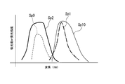
- the solar cell module concerning 20th Embodiment it is a figure which shows the light emission characteristic and absorption characteristic of the fluorescent substance disperse
- the solar cell module concerning 21st Embodiment it is a figure which shows the light emission characteristic and absorption characteristic of the fluorescent substance disperse
- the solar cell module concerning 22nd Embodiment it is a figure which shows the light emission characteristic and absorption characteristic of the fluorescent substance disperse
- FIG. 1 is a cross-sectional view showing a solar cell module 1 according to the first embodiment of the present invention.
- the solar cell module 1 includes a light collector 2 (light collector), a solar cell element 3 that receives light emitted from the end surface 2 c of the light collector 2, and a first main surface of the light collector 2.
- the first absorption filter 4 disposed on the 2a side via the air layer 7 and the second absorption surface 2b disposed on the second main surface 2b side opposite to the first main surface 2a of the light collector 2 via the air layer 7 2 absorption filter 5, light collector 2, solar cell element 3, first absorption filter 4, and frame 6 that holds second absorption filter 5 together.
- the first main surface 2a corresponds to the light incident surface described in the claims.
- the second main surface 2b corresponds to a surface opposite to the light incident surface described in the claims.
- the end surface 2c corresponds to the light emission surface described in the claims.
- the first absorption filter 4 and the second absorption filter 5 may be collectively referred to as “absorption filter”.
- the light collector 2 has a rectangular plate shape, and as an example, the length of one side is about 20 cm and the thickness is about 4 mm.
- the light collector 2 is a fluorescent light collector in which a phosphor 21 is dispersed in a transparent substrate 20.
- the light collector 2 absorbs the light incident from the first main surface 2a by the phosphor 21, propagates the light emitted from the phosphor 21 inside, and exits from the end surface 2c having a smaller area than the first main surface 2a.
- the transparent substrate 20 is made of a highly transparent organic material such as acrylic resin such as PMMA, polycarbonate resin, or transparent inorganic material such as glass.
- PMMA resin reffractive index 1.409 is used as the transparent substrate 20.
- the light collector 2 is formed by dispersing the phosphor 21 in this PMMA resin. Note that the refractive index of the light collector 2 is 1.50, which is about the same as that of the PMMA resin because the amount of the phosphor 21 dispersed is small.
- the phosphor 21 is an optical functional material that absorbs ultraviolet light or visible light, emits visible light or infrared light, and emits it.
- the optical functional material include organic phosphors.
- organic phosphors include coumarin dyes, perylene dyes, phthalocyanine dyes, stilbene dyes, cyanine dyes, polyphenylene dyes, xanthene dyes, pyridine dyes, oxazine dyes, chrysene dyes, thioflavine Dyes, perylene dyes, pyrene dyes, anthracene dyes, acridone dyes, acridine dyes, fluorene dyes, terphenyl dyes, ethene dyes, butadiene dyes, hexatriene dyes, oxazole dyes, coumarins Dyes, stilbene dyes, di- and triphenylmethane dyes, thiazole dyes, thiazin
- an inorganic phosphor can be used as the phosphor 21.
- various dyes direct dyes, acid dyes, basic dyes, disperse dyes, etc.
- one type of phosphor 21 is dispersed inside the light collector 2.
- the phosphor 21 absorbs orange light and emits red fluorescence.
- BASF Lumogen R305 (trade name) is used as the phosphor 21.
- the mixing ratio of the phosphors 21 was 0.02 wt% in mass percent concentration with respect to the transparent substrate (PMMA resin).
- the frame 6 is made of a frame such as aluminum and holds the outer peripheral portion of the light collector 2 and also holds the solar cell element 3, the first absorption filter 4, and the second absorption filter 5 together with the light collector 2.
- Each end surface 2c of the light collector 2 is hermetically sealed by the frame body 6 or a sealing member (not shown), and is shielded by the frame body 6 or the like so that external light (sunlight) is not irradiated.
- FIG. 2 is a diagram showing the light emission characteristics and absorption characteristics of the phosphor 21 used in the present embodiment.
- the horizontal axis represents wavelength (nm)
- the left vertical axis represents absorbance
- the right vertical axis represents emission intensity (au).
- the symbol Sp1 is the emission spectrum of the phosphor 21
- the symbol Sp2 is the absorption spectrum of the phosphor 21.
- the emission spectrum Sp1 of the phosphor 21 has a peak wavelength at approximately 610 nm.
- the absorption spectrum Sp2 of the phosphor 21 has a peak wavelength at approximately 570 nm.
- the phosphor 21 absorbs light having a wavelength of approximately 600 nm or less.
- phosphor 21 it is not limited to the case where one type of phosphor 21 is used, and a plurality of types (two types or three or more types) of phosphors may be used.
- the solar cell element 3 is arranged such that the light receiving surface faces the end surface 2 c of the light collector 2.
- the solar cell element 3 is preferably optically bonded to the end surface 2c.
- a known solar cell such as a silicon solar cell, a compound solar cell, a quantum dot solar cell, or an organic solar cell can be used.
- the compound type solar cell and quantum dot solar cell using a compound semiconductor are suitable as the solar cell element 3 since highly efficient electric power generation is possible.
- a GaAs solar cell that is a compound solar cell exhibiting high efficiency at the peak wavelength (610 nm) of the emission spectrum of the phosphor 21 is used.
- examples of compound solar cells include InGaP, GaAs, InGaAs, AlGaAs, Cu (In, Ga) Se 2 , Cu (In, Ga) (Se, S) 2 , CuInS 2 , CdTe, and CdS. It is done.
- examples of the quantum dot solar cell include Si and InGaAs. However, other types of solar cells such as Si and organic can be used depending on the price and application.
- the vertical width is about 4 mm.
- the vertical width of the solar cell element 3 is substantially equal to the thickness of the light collector 2.
- Each of the first absorption filter 4 and the second absorption filter 5 is a fluorescent absorption plate in which an absorption pigment that absorbs fluorescence is dispersed in a transparent plate.
- the absorbing dye a general-purpose absorbing dye can be used.
- FIG. 3 is a diagram showing the absorption characteristics of the absorbing dye.
- the horizontal axis represents wavelength (nm) and the vertical axis represents absorbance (au).
- the peak wavelengths of the absorption spectra of the respective absorbing dyes are different from each other.
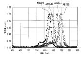
- FIG. 4 is a diagram showing the absorption characteristics of the absorption dye used in the absorption filter according to this embodiment.
- the horizontal axis represents wavelength (nm) and the vertical axis represents absorbance (au).
- the absorption filter a PMMA plate having a thickness of 0.5 mm mixed with 0.06% of ABS626, ABS647, ABS674, and ABS691 manufactured by Indigo Corporation is used as shown in FIG. Thereby, an absorption filter capable of absorbing a wavelength of approximately 600 nm to 720 nm can be obtained. For this reason, it is possible to make it difficult to see the light emission of the phosphor having a peak wavelength of the emission spectrum of approximately 610 nm.
- the absorption pigment dispersed in the absorption filter is dissolved in the PMMA resin serving as a binder.
- the absorbing dye When the absorbing dye is dissolved, scattering hardly occurs.
- the surface glare may increase due to the scattering of sunlight, or the probability that sunlight may enter the light collector may be reduced. For this reason, it is desirable to make the absorption filter less susceptible to scattering.
- the absorption filter may be selected according to the type of phosphor dispersed in the light collector. In particular, it is only necessary to cut light in a wavelength band that is perceived by human eyes. Therefore, as the absorption filter, an absorption filter that can cut in the visible light region (approximately 380 nm to 780 nm wavelength) may be used.
- FIG. 5 is a diagram showing the emission characteristics and absorption characteristics of the phosphor 21 dispersed in the light collector 2 according to the present embodiment, together with the absorption characteristics of the absorbing dye.
- the horizontal axis represents the wavelength (nm)
- the vertical axis represents the absorbance with respect to the absorption characteristics
- the emission intensity with respect to the light emission characteristics Reference numeral Sp1 is an emission spectrum of the phosphor 21
- reference numeral Sp2 is an absorption spectrum of the phosphor 21
- reference numeral Sp3 is an absorption spectrum of the absorption filter.
- the absorbance of the absorption filter with respect to the peak wavelength of the emission spectrum Sp1 of the phosphor 21 is larger than the absorbance with respect to the peak wavelength of the absorption spectrum Sp2 of the phosphor 21.
- the absorption filter has a smaller transmittance for the peak wavelength of the emission spectrum Sp1 of the phosphor 21 than for the transmittance of the phosphor 21 for the peak wavelength of the absorption spectrum Sp2.
- the shape of the absorption spectrum Sp3 of the absorption filter is such that it covers the emission spectrum Sp1 of the phosphor 21.
- the absorption filter has an absorption characteristic in a wavelength region longer than the wavelength of the short wavelength side end portion of the emission spectrum Sp1 of the phosphor 21, and the short wavelength side end portion of the emission spectrum Sp1 of the phosphor 21.
- the absorbance increases from the wavelength of 1 to the peak wavelength.
- the peak wavelength of the absorption spectrum Sp3 of the absorption filter substantially coincides with the peak wavelength of the emission spectrum Sp1 of the phosphor 21.
- “the wavelength at the end of the phosphor 21 on the short wavelength side of the emission spectrum Sp1” is defined as a wavelength that is 5% of the intensity at the peak wavelength of the emission spectrum Sp1 of the phosphor 21.
- the emission spectrum Sp1 of the phosphor 21 is shifted to a longer wavelength side than the absorption spectrum Sp2 by Stokes shift.
- the region where the emission spectrum Sp1 and the absorption spectrum Sp2 of the phosphor 21 do not overlap is large. Therefore, an absorption filter that can absorb most of the emission spectrum Sp1 of the phosphor 21 can be provided. Therefore, the absorption filter allows the absorption component of the phosphor 21 to transmit substantially 100% with respect to sunlight incident from the outside, and can absorb most of the light emission component of the phosphor 21.
- the apparent color of the light collector 2 is the emission color of the phosphor 21 used. According to the present embodiment, since the light emission of the phosphor 21 is absorbed by the absorption filter, the apparent color of the light collector 2 is a blackish or brownish color. As a result, it is possible to solve a problem such as an uncomfortable appearance. Further, even if an absorption filter is provided, the power generation efficiency is not lowered because there is almost no influence on the absorption spectrum Sp2 of the phosphor 21.
- the phosphor 21 that emits red light is dispersed in the light collector 2 of this embodiment, the color when the light collector 2 is viewed from above and below is red. In many cases, red is easily noticeable by some people and has a sense of incongruity. It is not suitable to provide such a light collector 2 on the roof or wall. According to this embodiment, the apparent color of the solar cell module 1 can be changed without impairing the power generation function.
- the peak wavelength of the emission spectrum Sp1 of the phosphor 21 dispersed in the light collector 2 and the peak wavelength of the absorption spectrum Sp3 of the absorption filter are substantially the same, light is emitted from the light collector 2.
- the light that has escaped up and down can be sufficiently absorbed by the absorption filter. Therefore, the apparent color of the solar cell module 1 can be made substantially black. Therefore, it is possible to provide the solar cell module 1 capable of suppressing the appearance of an uncomfortable feeling and aesthetics while solving the problems.
- the absorption filters installed above and below the light collector 2 are not necessarily the same.
- the appearance of the upper and lower surfaces of the solar cell module 1 does not necessarily have to be the same, and can be adjusted according to the user's preference.
- the characteristics of the absorption filter include (1) density and (2) color tone. In the absorption filters installed above and below the light collector 2, either (1) or (2) may be changed, or both may be changed.
- the color of the solar cell module 1 changed from red to blackish brown by the absorption filter according to the present embodiment.
- the red color often has a sense of incongruity with the color of the roof, but the discomfort with the color of the roof can be reduced by providing an absorption filter.
- sunlight is substantially 100% transmitted to the absorption band of the phosphor 21, the incident efficiency of sunlight on the light collector 2 is not reduced, and the amount of power generation is not reduced.
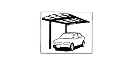
- FIGS. 6A to 6C are diagrams showing application examples of the solar cell module 1.
- FIG. 6A is a diagram illustrating an application example to a carport.
- FIG. 6B is a diagram illustrating an application example to a window.
- FIG. 6C is a diagram illustrating an application example to a wall of a building.
- the car may appear red and the car may look strange.
- the vehicle does not look red due to the action of the absorption filter, so that it is possible to prevent the vehicle from having an uncomfortable feeling.
- intense direct sunlight can be prevented, temperature rise in the vehicle and deterioration of articles in the vehicle can be suppressed.
- the weight can be reduced to about 40% as compared with a solar cell module having a configuration in which a conventional silicon substrate is spread.
- the support column and the base must be designed to withstand load, which is expensive. In some installation locations, the solar cell module may not be installed due to weight.
- the solar cell module 1 can be incorporated with substantially the same weight as the carport.
- red light may enter the room and feel uncomfortable. Moreover, even if the window is viewed from the exterior, the red color has a great influence on the surrounding landscape, so the landscape may be damaged.
- an adverse effect such as a sense of incongruity or a loss of scenery due to the action of the absorption filter. Further, particularly in summer, intense direct sunlight can be prevented, so that an increase in indoor temperature and deterioration of indoor articles can be suppressed.
- the windows can be installed with light weight as well as the carport.
- the wall of the building looks red, and the appearance of the building may be uncomfortable.
- the building wall can be installed with light weight as well as the carport. In order to install a conventional heavy solar cell module on the wall surface of a building, it is necessary to fix it vertically to the wall surface. Therefore, it must be performed by a stronger fixing method than installing on the roof, and the installation area of the solar cell module is limited.
- the solar cell module 1 since the solar cell module 1 that is lighter than the conventional one is used, a strong fixing method is not required. Therefore, the installation area of the solar cell module 1 can be greatly expanded.
- the absorption filter includes a first absorption filter 4 disposed on the first main surface 2 a side of the light collector 2 via the air layer 7, and air on the second main surface 2 b side of the light collector 2.
- positioned through the layer 7 was mentioned and demonstrated, it is not restricted to this.
- the absorption filter may have only the first absorption filter 4 disposed on the first main surface 2 a side of the light collector 2 via the air layer 7, or the second main surface 2 b of the light collector 2. You may have only the 2nd absorption filter 5 arrange
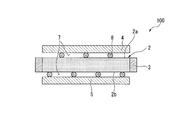
- FIG. 7 is a cross-sectional view showing a solar cell module 100 according to the second embodiment of the present invention.
- illustration of the phosphor and the frame dispersed in the light collector 2 is omitted.
- the solar cell module 100 of the present embodiment is different from the solar cell module 1 of the first embodiment in that a spacer 8 is disposed between the light collector 2 and the absorption filter.
- a spacer 8 is disposed between the light collector 2 and the absorption filter.
- symbol is attached
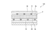
- a plurality of spacers 8 are arranged between the first main surface 2 a of the light collector 2 and the first absorption filter 4 and between the second main surface 2 b of the light collector 2 and the second absorption filter 5. .
- the plurality of spacers 8 are randomly arranged.
- the spacer 8 has a spherical shape, and its size is, for example, about 1 mm in diameter.
- PMMA resin reffractive index 1.49
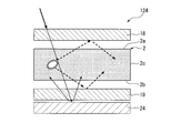
- the spacer 8 can keep the distance between the light collector 2 and the absorption filter constant, and the contact between the absorption filter and the light collector 2 is suppressed. Therefore, it is possible to suppress the light propagating through the light collector 2 from entering the absorption filter.
- the spacer 8 of this embodiment is spherical, the spacer 8 and the light collector 2 are in point contact. Therefore, the contact area between the spacer 8 and the light collector 2 can be minimized, and the light propagating through the light collector 2 can be reliably prevented from entering the absorption filter.
- the present invention is not limited to this.
- a silicon resin may be used as the spacer 8 or another resin may be used.
- an elastic buffer material such as rubber may be used. By using the cushioning material, it is possible to reduce the impact when an external impact or load is applied, and it is possible to provide a device that is highly resistant to external impact.
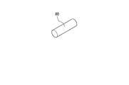
- the spacer 80 may be cylindrical.
- the size in this case is about 1 mm in diameter and about 1 cm in length.
- the spacer 80 is cylindrical, the spacer 80 and the absorption filter are in line contact, and the spacer 80 and the light collector 2 are in line contact. Therefore, according to the columnar spacer 80, it is easier to disperse external impacts than the spherical spacer 8.
- the inventor of the present application compared the resistance to impact between the cylindrical spacer 80 and the spherical spacer 8 in order to verify the effect when the spacer is cylindrical. Hereinafter, these comparison results will be described.
- FIG. 9 is a cross-sectional view showing a solar cell module 101 according to the third embodiment of the present invention.
- illustration of the phosphor and the frame dispersed in the light collector 2 is omitted.
- a spacer 81 is disposed between the light collector 2 and the absorption filter, and the area of the portion where the spacer 81 is in contact with the light collector 2 is determined by the spacer 81.
- the point which is smaller than the area of the part which touches an absorption filter differs from the solar cell module 100 of 2nd Embodiment.
- symbol is attached
- a plurality of spacers 81 are arranged between the first main surface 2 a of the light collector 2 and the first absorption filter 4 and between the second main surface 2 b of the light collector 2 and the second absorption filter 5. .
- the plurality of spacers 81 are arranged at a constant interval.
- the spacer 81 has a triangular prism shape, and its size is, for example, about 5 mm on a side and about 1 cm in length.
- the bottom of the spacer 81 is in contact with the absorption filter, and the vertex of the spacer 81 is in contact with the light collector 2.
- the spacer 81 has a triangular prism shape, the spacer 81 and the absorption filter are in surface contact, and the spacer 81 and the light collector 2 are in line contact. Therefore, according to the triangular prism-shaped spacer 81, it is easier to disperse external impacts than the spherical spacer 8. Therefore, resistance to impact can be improved.
- the present invention is not limited to this.
- a plurality of spacers 81 may be arranged at random.
- FIG. 10 is a cross-sectional view showing a solar cell module 102 according to the fourth embodiment of the present invention.
- FIG. 10 for the sake of convenience, illustration of the phosphor and the frame dispersed in the light collector 2 is omitted.
- a spacer 82 is disposed between the light collector 2 and the absorption filter, and the reflective layer 9 (reflective) is interposed between the spacer 82 and the light collector 2.
- the member is different from the solar cell module 101 of the third embodiment.
- symbol is attached
- a plurality of spacers 82 are arranged between the first main surface 2 a of the light collector 2 and the first absorption filter 4 and between the second main surface 2 b of the light collector 2 and the second absorption filter 5. .
- the plurality of spacers 82 are arranged with a certain interval.
- the spacer 82 has a triangular prism shape, and its size is, for example, about 5 mm on a side and about 1 cm in length.
- the bottom of the spacer 82 is in contact with the reflective layer 9 and the apex of the spacer 82 is in contact with the absorption filter.
- a reflective layer made of a dielectric multilayer film such as an ESR (Enhanced Special Reflector) reflective film (manufactured by 3M) can be used. If this material is used, a high reflectance of 98% or more can be realized under visible light.
- a reflective layer made of a metal film such as aluminum (Al), copper (Cu), gold (Au), silver (Ag) may be used.
- the spacer 82 has a triangular prism shape, the spacer 82 and the reflective layer 9 are in surface contact, and the spacer 82 and the absorption filter are in line contact. Therefore, according to the triangular prism-shaped spacer 82, it is easier to disperse external impacts than the spherical spacer 8. Therefore, resistance to impact can be improved.
- the present invention is not limited to this.
- a plurality of spacers 82 may be arranged at random.
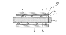
- FIG. 11 is a cross-sectional view showing a solar cell module 103 according to the fifth embodiment of the present invention.
- FIG. 11 for the sake of convenience, illustration of the phosphor and the frame dispersed in the light collector 2 is omitted.
- the solar cell module 103 of the present embodiment has a solar cell module 103 according to the second embodiment in that an infrared absorption filter 10 that absorbs infrared rays is disposed on the first main surface 2 a side of the light collector 2. Different from the battery module 100.
- symbol is attached
- the infrared absorption filter 10 is disposed on the surface of the first absorption filter 4 on the first main surface 2a side.
- the plurality of spacers 8 are disposed between the first main surface 2 a of the light collector 2 and the infrared absorption filter 10.
- the infrared absorption filter 10 As the infrared absorption filter 10, a commercially available infrared cut film, Sumipex 000 Clear (manufactured by Sumitomo Chemical Co., Ltd.) can be used.
- FIG. 12 is a diagram showing the absorption characteristics of the infrared absorption filter 10.
- the horizontal axis represents wavelength (nm) and the vertical axis represents light transmittance (%).
- the absorption characteristics of Sumipex 000 clear with different thicknesses as the infrared absorption filter 10 are shown together with the absorption characteristics of soda glass 3 mm (soda glass having a thickness of 3 mm) as a comparative example.
- the thickness of Sumipex 000 clear was 2 mm, 3 mm, and 6 mm.
- the light transmission spectrum of Sumipex 000 Clear has a drop in the infrared region.
- the light transmission spectrum of Sumipex 000 clear has a maximum depression portion at about 1400 nm, that is, a wavelength that absorbs infrared light most (hereinafter referred to as a light absorption peak wavelength).
- the light transmittance at the light absorption peak wavelength of the light transmission spectrum of Sumipex 000 Clear is smaller than the light transmittance at a wavelength of 1400 nm of the light transmission spectrum of soda glass 3 mm.
- the light transmittance at the light absorption peak wavelength of the light transmission spectrum of Sumipex 000 clear decreases as the thickness increases.
- the light transmittance at the light absorption peak wavelength of the light transmission spectrum of Sumipex 000 clear is about 70% at a thickness of 2 mm, about 60% at a thickness of 3 mm, and about 45% at a thickness of 6 mm.
- infrared absorption filter is not provided on the first main surface side of the light collecting plate, infrared rays are incident on the light collecting plate, so that the light collecting plate may be heated by infrared rays to increase in temperature and become hot. . In this case, the light collector may be along or deformed.
- infrared rays are absorbed by the infrared absorption filter 10, it is possible to prevent infrared rays from entering the light collector 2. Therefore, even if sunlight is irradiated on the solar cell module for a long time, the light collector 2 is not heated by infrared rays, and the temperature rise of the light collector 2 can be suppressed. Accordingly, warpage and deformation of the light collector 2 can be suppressed.
- the present invention is not limited thereto.
- an absorption dye for absorbing infrared rays may be mixed in the absorption filter.
- Lumogen IR series manufactured by BASF can be used as the absorbing dye to be mixed.
- the inventor of the present application compared the temperature of the light collector when the infrared absorption filter 10 is provided and when the infrared absorption filter 10 is not provided, when the infrared ray is continuously irradiated. .
- these comparison results will be described.
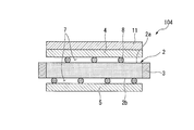
- FIG. 13 is a cross-sectional view showing a solar cell module 104 according to the sixth embodiment of the present invention.
- illustration of the phosphor and the frame dispersed in the light collector 2 is omitted.
- the solar cell module 104 of the present embodiment is that the antireflection layer 11 is disposed on the surface of the first absorption filter 4 on the side opposite to the light collector 2. Different from the battery module 100.
- symbol is attached
- a visible multi-AR coat (window) (made by CBC Optics), which is an antireflection film for visual recognition made of a dielectric multilayer film, can be used.
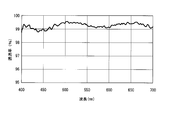
- FIG. 14 is a diagram showing the reflection characteristics of the antireflection layer 11.
- the horizontal axis represents wavelength (nm) and the vertical axis represents transmittance (%).
- the reflection characteristics of the visible multi-AR coating (window) as the antireflection layer 11 are shown.
- the visible multi-AR coat has an average transmittance of 99% or more in the visible range.
- the inventor of the present application compared the state of surface reflection when sunlight is incident between the case where the antireflection layer 11 is provided and the case where the antireflection layer 11 is not provided. .
- these comparison results will be described.
- the reflectance of the solar cell module surface was confirmed for each of the solar cell module provided with the antireflection layer 11 and the solar cell module not provided with the antireflection layer 11.
- the reflectance of the solar cell module surface was about 4%. Although it was about 4%, it was quite dazzling when sunlight was incident, and the fluorescent color was glaring.
- the reflectance of the solar cell module surface was about 0.1%. Even when sunlight was incident, it was hardly reflected and the appearance was much softer.
- the antireflection layer 11 By providing the antireflection layer 11 in this way, the surface reflection was suppressed, the apparent glare was lost, and the sense of incongruity disappeared. Moreover, since the reflectance can be kept low, the incidence rate of sunlight on the light collector is increased. The power generation efficiency was improved by 0.5% compared to the case where the antireflection layer 11 was not provided.
- FIG. 15 is a cross-sectional view showing a solar cell module 105 according to the seventh embodiment of the present invention.
- FIG. 15 for the sake of convenience, illustration of the phosphor and the frame dispersed in the light collector 2 is omitted.
- the solar cell module 105 of the present embodiment has a reflection plate 12 (reflective layer) disposed on the surface (lower surface) opposite to the light collector 2 of the second absorption filter 5.
- positioned at the surface (lower surface) on the opposite side to the 2nd absorption filter 5 of the board 12 differs from the solar cell module 100 of 2nd Embodiment.
- symbol is attached
- the reflector 12 is provided on the lower surface of the second absorption filter 5 via an adhesive (not shown).
- an Al reflecting plate can be used as the reflecting plate 12. Thereby, the sunlight incident from above and the light emitting component from the light collector 2 can be reflected by substantially 100%.
- the reflecting plate 12 you may use Ag reflecting plate, an ESR reflecting film (made by 3M company), etc.
- the scattering plate 13 is provided on the lower surface of the reflecting plate 12 via an adhesive (not shown).
- an adhesive not shown.
- a white PET resinous white scattering plate can be used as the scattering plate 13.
- FIG. 16 is a diagram for explaining the operation of the solar cell module 105 according to the present embodiment.
- illustration of components other than the second absorption filter 5, the reflection plate 12, and the scattering plate 13 is omitted.
- the solar cell module 105 For example, by installing the solar cell module 105 on a roof or a wall, the light emitting component incident from the upper surface of the second absorption filter 5 is cut on the side opposite to the light incident surface of the solar cell module 105.
- the solar cell module 105 is installed in the carport, on the side opposite to the light incident surface of the solar cell module 105, light incident from the lower surface of the scattering plate 13 is scattered downward by the scattering plate 13 or scattered light. Is reflected downward by the reflector 12. Therefore, when the carport is viewed from below, it looks white or gray.
- the appearance (color) from the lower surface of the solar cell module 105 can be changed. Since the fluorescent color from the light collector 2 is cut, a calm color can be obtained. Moreover, since infrared rays are reflected upward by the reflecting plate 12, it is possible to suppress a temperature rise in the lower surface side portion of the solar cell module 105.
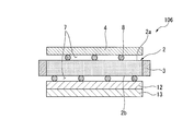
- FIG. 17 is a cross-sectional view showing a solar cell module 106 according to the eighth embodiment of the present invention.
- illustration of the phosphor and the frame dispersed in the light collector 2 is omitted.
- the solar cell module 106 of this embodiment is different from the solar cell module 105 according to the seventh embodiment in that the second absorption filter 5 is not provided. That is, in this embodiment, the absorption filter has only the first absorption filter 4.
- symbol is attached
- the reflector 12 is disposed on the second main surface 2b side of the light collector 2 via the air layer 7.
- the plurality of spacers 8 are disposed between the second main surface 2 b of the light collector 2 and the reflecting plate 12.
- the configuration of the apparatus can be simplified.
- FIG. 18 is a cross-sectional view showing a solar cell module 107 according to the ninth embodiment of the present invention.
- illustration of the phosphor and the frame dispersed in the light collector 2 is omitted.
- the solar cell module 107 of the present embodiment is different from the solar cell module 105 according to the seventh embodiment in that a black plate 14 (black layer) is provided instead of the scattering plate 13. .
- a black plate 14 black layer
- symbol is attached
- the black plate 14 is provided on the lower surface of the reflecting plate 12 via an adhesive (not shown).
- the apparent color from the lower surface of the solar cell module 107 can be black.
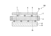
- FIG. 19 is a cross-sectional view showing a solar cell module 108 according to the tenth embodiment of the present invention.
- FIG. 19 for the sake of convenience, illustration of the phosphor and the frame dispersed in the light collector 2 is omitted.
- the solar cell module 108 of the present embodiment is different from the solar cell module 107 according to the ninth embodiment in that the second absorption filter 5 is not provided. That is, in this embodiment, the absorption filter has only the first absorption filter 4.
- symbol is attached
- the reflector 12 is disposed on the second main surface 2b side of the light collector 2 via the air layer 7.
- the plurality of spacers 8 are disposed between the second main surface 2 b of the light collector 2 and the reflecting plate 12.
- the configuration of the apparatus can be simplified.
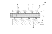
- FIG. 20 is a sectional view showing a solar cell module 109 according to the eleventh embodiment of the present invention.
- illustration of the phosphor and the frame dispersed in the light collector 2 is omitted.
- the solar cell module 109 of this embodiment is different from the solar cell module 105 according to the seventh embodiment in that a colored plate 15 (colored layer) is provided instead of the scattering plate 13. .
- a colored plate 15 colored layer
- symbol is attached
- the colored plate 15 is provided on the lower surface of the reflecting plate 12 via an adhesive (not shown).
- the colored plate 15 is colored brown.
- the colored plate 15 is not limited to brown and can be appropriately colored in a preferable color.
- the apparent color from the lower surface of the solar cell module 109 can be brown.
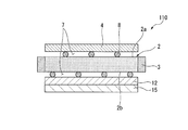
- FIG. 21 is a cross-sectional view showing a solar cell module 110 according to the twelfth embodiment of the present invention.
- FIG. 21 for the sake of convenience, illustration of the phosphor and the frame dispersed in the light collector 2 is omitted.
- the solar cell module 110 of this embodiment is different from the solar cell module 109 according to the eleventh embodiment in that the second absorption filter 5 is not provided. That is, in this embodiment, the absorption filter has only the first absorption filter 4.
- symbol is attached
- the reflector 12 is disposed on the second main surface 2b side of the light collector 2 via the air layer 7.
- the plurality of spacers 8 are disposed between the second main surface 2 b of the light collector 2 and the reflecting plate 12.
- the configuration of the apparatus can be simplified.
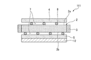
- FIG. 22 is a sectional view showing a solar cell module 111 according to the thirteenth embodiment of the present invention.
- illustration of the phosphor and the frame dispersed in the light collector 2 is omitted.
- the solar cell module 111 of this embodiment is different from the solar cell module 105 according to the seventh embodiment in that the scattering plate 13 is not provided. That is, in the present embodiment, only the reflection plate 12 is disposed on the surface (lower surface) opposite to the light collector 2 of the second absorption filter 5.
- symbol is attached
- the appearance from the lower surface of the solar cell module 111 is the light itself reflected by the reflector 12. Therefore, this configuration can be employed when the lower surface side of the solar cell module 111 is brightened or mirror reflection is desired.
- FIG. 23 is a cross-sectional view showing a solar cell module 112 according to the fourteenth embodiment of the present invention.
- illustration of the phosphor and the frame dispersed in the light collector 2 is omitted.
- the solar cell module 112 of this embodiment is different from the solar cell module 111 according to the thirteenth embodiment in that the second absorption filter 5 is not provided. That is, in this embodiment, the absorption filter has only the first absorption filter 4.
- symbol is attached
- the reflector 12 is disposed on the second main surface 2b side of the light collector 2 via the air layer 7.
- the plurality of spacers 8 are disposed between the second main surface 2 b of the light collector 2 and the reflecting plate 12.
- the configuration of the apparatus can be simplified.
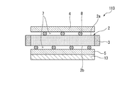
- FIG. 24 is a cross-sectional view showing a solar cell module 113 according to the fifteenth embodiment of the present invention.
- illustration of the phosphor and the frame dispersed in the light collector 2 is omitted for convenience.
- the solar cell module 113 of this embodiment is different from the solar cell module 111 according to the thirteenth embodiment in that a scattering plate 13 is provided instead of the reflection plate 12. That is, in the present embodiment, only the scattering plate 13 is disposed on the surface (lower surface) opposite to the light collector 2 of the second absorption filter 5.
- symbol is attached
- the appearance from the lower surface of the solar cell module 113 is the light itself scattered by the scattering plate 13. Therefore, the apparent color from the lower surface of the solar cell module 113 is almost white.
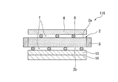
- FIG. 25 is a cross-sectional view showing a solar cell module 114 according to the sixteenth embodiment of the present invention.
- illustration of the phosphor and the frame dispersed in the light collector 2 is omitted.
- the solar cell module 114 of this embodiment is different from the solar cell module 113 according to the fifteenth embodiment in that the second absorption filter 5 is not provided. That is, in this embodiment, the absorption filter has only the first absorption filter 4.
- symbol is attached
- the scattering plate 13 is disposed on the second main surface 2 b side of the light collector 2 via the air layer 7.
- the plurality of spacers 8 are disposed between the second main surface 2 b of the light collector 2 and the scattering plate 13.
- the configuration of the apparatus can be simplified.
- FIG. 26 is a sectional view showing a solar cell module 115 according to the seventeenth embodiment of the present invention.
- illustration of the phosphor and the frame dispersed in the light collector 2 is omitted.
- the solar cell module 115 of the present embodiment is that the black plate 14 is provided on the surface (lower surface) opposite to the second absorption filter 5 of the scattering plate 13 in the fifteenth embodiment. This is different from the solar cell module 113 according to the above.
- symbol is attached
- the black plate 14 is provided on the lower surface of the scattering plate 13 via an adhesive (not shown).
- the apparent color from the lower surface of the solar cell module 115 can be black.
- FIG. 27 is a cross-sectional view showing a solar cell module 116 according to the eighteenth embodiment of the present invention.
- illustration of the phosphor and the frame dispersed in the light collector 2 is omitted.
- the solar cell module 116 of this embodiment is different from the solar cell module 115 according to the sixteenth embodiment in that the second absorption filter 5 is not provided. That is, in this embodiment, the absorption filter has only the first absorption filter 4.
- symbol is attached
- the scattering plate 13 is disposed on the second main surface 2 b side of the light collector 2 via the air layer 7.
- the plurality of spacers 8 are disposed between the second main surface 2 b of the light collector 2 and the scattering plate 13.
- the configuration of the apparatus can be simplified.
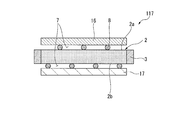
- FIG. 28 is a cross-sectional view showing a solar cell module 117 according to the nineteenth embodiment of the present invention.
- FIG. 28 for the sake of convenience, illustration of the phosphor and the frame dispersed in the light collector 2 is omitted.
- the solar cell module 117 includes the light collector 2, the solar cell element 3, and the first phosphor layer 16 disposed on the first main surface 2 a side of the light collector 2 via the air layer 7.
- the second phosphor layer 17 disposed on the second main surface 2b side of the light collector 2 with the air layer 7 interposed between the first main surface 2a of the light collector 2 and the first phosphor layer 16
- a plurality of spacers 8 are provided between each of the second main surface 2b of the optical plate 2 and the second phosphor layer 17.
- the first phosphor layer 16 and the second phosphor layer 17 may be collectively referred to as “phosphor layer”.
- symbol is attached
- the phosphor layer in addition to the above-described optical functional material, a mixture of ABS694, IRA735, IRA742, IRA751, IRA764, IRA788, etc. manufactured by Indigo Corporation is used. Thereby, a phosphor layer capable of absorbing light in the visible light region can be obtained.
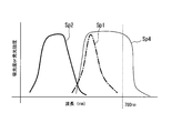
- FIG. 29 is a diagram showing the emission characteristics and absorption characteristics of the phosphor dispersed in the light collector 2 according to the present embodiment, together with the absorption characteristics of the phosphor layer.
- the horizontal axis represents wavelength (nm)
- the vertical axis represents absorbance with respect to absorption characteristics
- the emission intensity with respect to light emission characteristics Reference numeral Sp1 is an emission spectrum of the phosphor
- reference numeral Sp2 is an absorption spectrum of the phosphor
- reference numeral Sp4 is an absorption spectrum of the phosphor layer.
- the shape of the absorption spectrum Sp4 of the phosphor layer is such that it covers the emission spectrum Sp1 of the phosphor.
- the phosphor layer has an absorption characteristic in a wavelength region longer than the wavelength of the short wavelength side end of the phosphor emission spectrum Sp1, and the phosphor layer has an end of the short wavelength side of the phosphor emission spectrum Sp1.
- the absorbance increases from the wavelength toward the peak wavelength.
- the peak wavelength of the absorption spectrum Sp4 of the phosphor layer exists in a wide band.
- the peak wavelength on the short wavelength side of the absorption spectrum Sp4 of the phosphor layer and the peak wavelength of the emission spectrum Sp1 of the phosphor substantially coincide.
- the peak wavelength on the long wavelength side of the absorption spectrum Sp4 of the phosphor layer and the wavelength of 780 nm, which is the terminal wavelength in the visible light region, generally coincide. That is, the peak wavelength of the absorption spectrum Sp4 of the phosphor layer extends from the peak wavelength of the emission spectrum Sp1 of the phosphor to a wavelength of 780 nm.
- “the wavelength at the end of the phosphor emission spectrum Sp1 on the short wavelength side” is defined as a wavelength that is 5% of the intensity at the peak wavelength of the phosphor emission spectrum Sp1.
- the peak wavelength of the absorption spectrum Sp4 of the phosphor layer is spread over a wide wavelength range of not less than the peak wavelength of the emission spectrum Sp1 of the phosphor dispersed in the light collector 2 and not more than 780 nm,
- the light emitted from the light collector 2 and exiting up and down can be sufficiently absorbed by the phosphor layer. That is, all light in the visible light region can be absorbed by the phosphor layer. Therefore, the apparent color of the solar cell module 117 can be made substantially black.
- the phosphor layer includes the first phosphor layer 16 disposed on the first main surface 2a side of the light collector 2 via the air layer 7 and the second main surface 2b side of the light collector 2.
- the present invention is not limited to this.
- the phosphor layer may have only the first phosphor layer 16 disposed on the first main surface 2 a side of the light collector 2 via the air layer 7, or the second main surface of the light collector 2.
- You may have only the 2nd fluorescent substance layer 17 arrange
- FIG. 30 is a diagram showing the light emission characteristics and absorption characteristics of the phosphor dispersed in the light collector 2 together with the light emission characteristics and absorption characteristics of the phosphor layer in the twentieth embodiment of the present invention.
- the horizontal axis represents wavelength (nm)
- the vertical axis represents absorbance with respect to absorption characteristics
- Reference numeral Sp1 is an emission spectrum of the phosphor
- reference numeral Sp2 is an absorption spectrum of the phosphor
- reference numeral Sp5 is an emission spectrum of the phosphor layer
- reference numeral Sp6 is an absorption spectrum of the phosphor layer.
- illustration of a solar cell module is abbreviate
- the peak wavelength of the emission spectrum Sp5 of the phosphor layer is larger than the wavelength range of visible light (780 nm).
- the phosphor layer has light emission characteristics in a wavelength region longer than the wavelength region of visible light (780 nm).
- the shape of the absorption spectrum Sp6 of the phosphor layer is such that it covers the emission spectrum Sp1 of the phosphor.
- the phosphor layer has an absorption characteristic in a wavelength region longer than the wavelength of the short wavelength side end of the phosphor emission spectrum Sp1, and the phosphor layer has an end of the short wavelength side of the phosphor emission spectrum Sp1.
- the absorbance increases from the wavelength toward the peak wavelength.
- the peak wavelength of the absorption spectrum Sp6 of the phosphor layer and the peak wavelength of the emission spectrum Sp1 of the phosphor substantially coincide.
- “the wavelength at the end of the phosphor emission spectrum Sp1 on the short wavelength side” is defined as a wavelength that is 5% of the intensity at the peak wavelength of the phosphor emission spectrum Sp1.
- the peak wavelength of the emission spectrum Sp1 of the phosphor dispersed on the light collector 2 and the peak wavelength of the absorption spectrum Sp6 of the phosphor layer are approximately the same, light is emitted from the light collector 2.
- the light that has escaped up and down can be sufficiently absorbed by the phosphor layer.
- the emission wavelength of the phosphor layer exists in a wavelength range longer than the wavelength range of visible light (780 nm), the light emission component of the phosphor layer is invisible. Therefore, the apparent color of the solar cell module can be brown or substantially black.
- FIG. 31 is a diagram showing the emission characteristics and absorption characteristics of the phosphor dispersed in the light collector 2 together with the emission characteristics and absorption characteristics of the phosphor layer in the twenty-first embodiment of the present invention.
- the horizontal axis represents wavelength (nm)
- the vertical axis represents absorbance with respect to absorption characteristics
- Reference numeral Sp1 is an emission spectrum of the phosphor
- reference numeral Sp2 is an absorption spectrum of the phosphor
- reference numeral Sp7 is an emission spectrum of the phosphor layer
- reference numeral Sp8 is an absorption spectrum of the phosphor layer.
- illustration of a solar cell module is abbreviate
- the peak wavelength of the emission spectrum Sp7 of the phosphor layer is smaller than the peak wavelength of the emission spectrum Sp1 of the phosphor.
- the light emitted from the phosphor and the light emitted from the phosphor layer are mixed to form light that is closer to an achromatic color than the light emitted from the phosphor. For example, white light is formed.
- the peak wavelength of the absorption spectrum Sp8 of the phosphor layer is shorter than the wavelength at the end on the short wavelength side of the absorption spectrum Sp2 of the phosphor.
- the phosphor layer absorbs light having a shorter wavelength than the peak wavelength of the phosphor absorption spectrum Sp2.
- “the wavelength at the end of the phosphor absorption spectrum Sp2 on the short wavelength side” is defined as a wavelength that is 5% of the intensity at the peak wavelength of the phosphor absorption spectrum Sp2.
- the light emitted from the phosphor and the light emitted from the phosphor layer are mixed, light close to achromatic color is formed, which reduces the uncomfortable appearance of the solar cell module. can do.
- the apparent color of the solar cell module can be adjusted to a desired color.
- FIG. 32 is a diagram showing the emission characteristics and absorption characteristics of the phosphor dispersed in the light collector 2 together with the emission characteristics and absorption characteristics of the phosphor layer in the twenty-second embodiment of the present invention.
- the horizontal axis represents the wavelength (nm)
- the vertical axis represents the absorbance with respect to the absorption characteristics
- Reference numeral Sp1 is an emission spectrum of the phosphor
- reference numeral Sp2 is an absorption spectrum of the phosphor
- reference numeral Sp9 is an emission spectrum of the phosphor layer
- reference numeral Sp10 is an absorption spectrum of the phosphor layer.
- illustration of a solar cell module is abbreviate
- the peak wavelength of the emission spectrum Sp9 of the phosphor layer is smaller than the peak wavelength of the emission spectrum Sp1 of the phosphor.
- the light emitted from the phosphor and the light emitted from the phosphor layer are mixed to form light that is closer to an achromatic color than the light emitted from the phosphor. For example, white light is formed.
- the emission spectrum Sp9 of the phosphor layer is covered with the absorption spectrum Sp10 of the phosphor 21.
- the absorbance with respect to the peak wavelength of the absorption spectrum Sp2 of the phosphor is larger than the emission intensity with respect to the peak wavelength of the emission spectrum Sp9 of the phosphor layer.
- the peak wavelength of the emission spectrum Sp9 of the phosphor layer and the peak wavelength of the absorption spectrum Sp2 of the phosphor substantially coincide.
- the shape of the absorption spectrum Sp10 of the phosphor layer is such that it covers the emission spectrum Sp1 of the phosphor.
- the phosphor layer has an absorption characteristic in a wavelength region longer than the wavelength of the short wavelength side end of the phosphor emission spectrum Sp1, and the phosphor layer has an end of the short wavelength side of the phosphor emission spectrum Sp1.
- the absorbance increases from the wavelength toward the peak wavelength.
- the peak wavelength of the absorption spectrum Sp6 of the phosphor layer and the peak wavelength of the emission spectrum Sp1 of the phosphor substantially coincide.
- “the wavelength at the end of the phosphor emission spectrum Sp1 on the short wavelength side” is defined as a wavelength that is 5% of the intensity at the peak wavelength of the phosphor emission spectrum Sp1.
- the light emitted from the phosphor and the light emitted from the phosphor layer are mixed to form light close to achromatic color, thereby reducing the uncomfortable appearance of the solar cell module. be able to.
- the apparent color of the solar cell module can be adjusted to a desired color.
- the peak wavelength of the emission spectrum Sp1 of the phosphor dispersed on the light collector 2 and the peak wavelength of the absorption spectrum Sp10 of the phosphor layer are substantially the same, light is emitted from the light collector 2 and escapes vertically. Can be sufficiently absorbed by the phosphor layer.
- the peak wavelength of the absorption spectrum Sp2 of the phosphor dispersed on the light collector 2 and the peak wavelength of the emission spectrum Sp9 of the phosphor layer are approximately the same, the light emitted from the phosphor layer is collected again.
- the amount of light propagating through the light collector 2 can be increased by entering the light plate 2 and re-emitting the phosphor. Therefore, power generation efficiency can be improved.
- a fluorescent material that emits light having a complementary color relationship with the light emitted from the phosphor dispersed in the light collector 2 can be used as the phosphor layer.
- a fluorescent material that emits blue light can be used as the phosphor layer.
- a fluorescent material (DeepUV excited luminescent molecule) that absorbs light in the far ultraviolet region (230 nm to 320 nm) of the sunlight and emits light in the blue region (380 nm to 530 nm) is used. it can.
- FIGS. 33A to 33D are diagrams showing examples of Deep UV excited luminescent molecules together with absorption characteristics and luminescence characteristics.
- the solid line represents the absorption spectrum of the Deep UV excited luminescent molecule
- the broken line represents the emission spectrum of the Deep UV excited luminescent molecule.
- the horizontal axis represents wavelength (nm)
- the vertical axis represents absorbance with respect to absorption characteristics
- the Deep UV excited luminescent molecule shown in FIG. 33A is p-Terphenyl.
- the peak wavelength of the absorption spectrum (solid line) of p-Terphenyl is approximately 270 nm, and the peak wavelength of the emission spectrum (dashed line) is approximately 350 nm.
- the Deep UV excited luminescent molecule shown in FIG. 33B is POPOP.
- the POPOP absorption spectrum (solid line) has a peak wavelength of approximately 340 nm, and the emission spectrum (broken line) has a peak wavelength of approximately 420 nm.
- the Deep UV excited luminescent molecule shown in FIG. 33C is Coumarin® 120.
- the peak wavelength of the absorption spectrum (solid line) of Coumarin® 120 is approximately 360 nm, and the peak wavelength of the emission spectrum (dashed line) is approximately 430 nm.
- the Deep UV excited luminescent molecule shown in FIG. 33D is p-Quaterphenyl.
- the peak wavelength of the absorption spectrum (solid line) of p-Quaterphenyl is approximately 300 nm, and the peak wavelength of the emission spectrum (dashed line) is approximately 380 nm.
- a fluorescent material that absorbs light emitted from the phosphor 21 dispersed in the light collector 2 and emits light in a blue region can be used.
- FIG. 34A and FIG. 33B are diagrams showing examples of the fluorescent material of the phosphor layer together with the absorption characteristics and the light emission characteristics.
- the solid line represents the absorption spectrum of the fluorescent material in the phosphor layer
- the broken line represents the emission spectrum of the fluorescent material in the phosphor layer.
- the horizontal axis represents wavelength (nm)
- the vertical axis represents absorbance with respect to absorption characteristics
- emission intensity with respect to light emission characteristics are diagrams showing examples of the fluorescent material of the phosphor layer together with the absorption characteristics and the light emission characteristics.
- the fluorescent material of the phosphor layer shown in FIG. 34A is 1,1′-Bis (4-sulfobutyl) -3,3,3 ′, 3′-tetramethylindodicarbocyanine betaine sodium salt.
- the peak wavelength of the absorption spectrum (solid line) is approximately 641 nm, and the peak wavelength of the emission spectrum (broken line) is approximately 480 nm.
- the fluorescent material of the phosphor layer shown in FIG. 34B is 1,1′-Dibutyl-3,3,3 ′, 3′-tetramethylindodicarbocyanine perchlorate.
- the peak wavelength of the absorption spectrum (solid line) is approximately 642 nm, and the peak wavelength of the emission spectrum (dashed line) is approximately 485 nm.
- the function as an absorption filter can also be given to a fluorescent substance layer by reducing the luminous efficiency of the fluorescent material of a fluorescent substance layer.
- a method of lowering the luminous efficiency of the fluorescent material of the phosphor layer a method of mixing a fluorescent material having a high concentration higher than the concentration quenching into the phosphor layer, a material that quenches the fluorescent material in the phosphor layer (quenching agent) ) And a method using a material having a low fluorescence quantum yield as the fluorescent material of the phosphor layer.
- emitted from the fluorescent substance by mixing the light radiated
- the configuration is not limited thereto.
- the light emitted from the phosphor and the light reflected by the bandpass filter are mixed, so that the phosphor A configuration in which light closer to an achromatic color than the emitted light is formed may be used.
- FIG. 35 is a cross-sectional view showing a solar cell module 118 according to the 23rd embodiment of the present invention.
- the angle ⁇ means an angle formed between the normal line of the first main surface 2a and the optical axis of the light incident on the first main surface 2a (hereinafter referred to as an incident angle).
- an incident angle means an angle formed between the normal line of the first main surface 2a and the optical axis of the light incident on the first main surface 2a (hereinafter referred to as an incident angle).
- an incident angle the phosphors and the frame body dispersed in the light collector 2 are not shown.
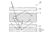
- the solar cell module 118 includes the light collector 2, the solar cell element 3, and the first bandpass filter 18 disposed on the first main surface 2 a side of the light collector 2 via the air layer 7.
- a second band-pass filter 19 disposed on the second main surface 2b side of the light collector 2 with an air layer 7 interposed therebetween.
- the first band pass filter 18 and the second band pass filter 19 may be collectively referred to as “band pass filters”.
- symbol is attached
- the bandpass filter according to the present embodiment is made of a dielectric multilayer film and is configured to reflect red light.
- the peak wavelength of the first reflection spectrum is larger than the peak wavelength of the emission spectrum of the phosphor, and the reflection band of the second reflection spectrum has an increased incident angle ⁇ . Accordingly, the peak wavelength of at least one of the second reflection spectra is smaller than the peak wavelength of the emission spectrum of the phosphor.
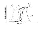
- FIG. 36 is a diagram showing the emission characteristics and absorption characteristics of the phosphor 21 dispersed in the light collector 2 according to this embodiment, together with the reflection characteristics of the bandpass filter.
- the horizontal axis represents wavelength (nm)
- the vertical axis represents absorbance with respect to absorption characteristics, emission intensity with respect to light emission characteristics, and reflectance with respect to reflection characteristics.
- Reference sign Sq1 is the emission spectrum of the phosphor
- reference sign Sq2 is the absorption spectrum of the fluorescent substance
- reference sign Sr1 is the first reflection spectrum of the bandpass filter
- reference sign Sr2 is the second reflection spectrum of the bandpass filter.
- the rising position of the first reflection spectrum Sr1 is approximately equal to the wavelength at the position where the emission spectrum Sq1 of the phosphor and the absorption spectrum Sq2 of the phosphor intersect, and The rising position of the reflection spectrum Sr2 of 2 is smaller than the peak wavelength of the emission spectrum Sq1 of the phosphor.
- the rising position of the first reflection spectrum Sr1 is larger than the peak wavelength of the absorption spectrum Sq2 of the phosphor.
- the rising position of the first reflection spectrum Sr1 does not have to coincide with the wavelength at the position where the emission spectrum Sq1 of the phosphor and the absorption spectrum Sq2 of the phosphor intersect, and the peak wavelength of Sq1 of the emission spectrum of the phosphor It may be larger or smaller.
- the sunlight that enters from the outside a component that is reflected by the bandpass filter and does not enter the light collector 2 is generated. In this case, a large overlap between the reflection spectrum of the bandpass filter and the absorption spectrum of the phosphor is not preferable because the light collector 2 does not emit light.
- the light collector 2 emits light with some loss. Therefore, it is important that the light emitted from the light collector 2 is reflected by the bandpass filter as much as possible and confined within the light collector 2. From such a viewpoint, the ideal position of the rising position of the first reflection spectrum Sr1 coincides with the position where the emission spectrum Sq1 of the phosphor and the absorption spectrum Sq2 of the phosphor intersect.
- the shape of the second reflection spectrum Sr2 covers the emission spectrum Sq1 of the phosphor.
- the bandpass filter has a reflection characteristic of the second reflection spectrum Sr2 in a wavelength region longer than the wavelength of the short wavelength side end of the phosphor emission spectrum Sq1, and the phosphor emission spectrum Sq1
- the reflectance increases from the wavelength at the end on the short wavelength side toward the peak wavelength.
- the “rising position of the first reflection spectrum Sr1” is defined as the wavelength at which the reflectance of the bandpass filter when viewed from the front is 5%.
- the “wavelength at the end of the phosphor emission spectrum Sq1 on the short wavelength side” is defined as a wavelength that is 5% of the intensity at the peak wavelength of the phosphor emission spectrum Sq1.
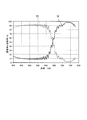
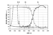
- FIG. 37 is a diagram showing transmission characteristics and reflection characteristics when light is incident from the front direction on the bandpass filter according to the present embodiment (at the time of front incidence).
- the horizontal axis represents wavelength (nm)
- the vertical axis represents transmittance (%) for transmission characteristics
- reflectance (%) for reflection characteristics Reference symbol St is a transmission spectrum at the front incidence of the bandpass filter
- reference symbol St is a reflection spectrum at the front incidence of the bandpass filter.
- the transmission band of the transmission spectrum St at the front incidence of the bandpass filter exists in the range of about 400 nm to 630 nm, and the reflection band of the reflection spectrum Sr is about 650 nm to 780 nm. Exists in the range.
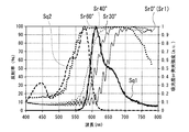
- 38A and 38B are diagrams showing the incident angle dependence of the reflection characteristics of the bandpass filter according to this embodiment, together with the emission spectrum and absorption spectrum of the phosphor dispersed in the light collector 2.
- the horizontal axis represents wavelength (nm)
- the left vertical axis represents reflectance (%)
- the right vertical axis represents absorbance with respect to absorption characteristics
- Sq1 is the emission spectrum of the phosphor
- Sq2 is the absorption spectrum of the phosphor.
- the reflection band of the reflection spectrum Sr of the bandpass filter is shifted to the short wavelength side as the incident angle ⁇ increases.
- the rising position of the reflection spectrum Sr0 ° of the bandpass filter is substantially equal to the peak wavelength of the emission spectrum Sq1 of the phosphor.
- the rising position of the reflection spectrum Sr0 ° of the bandpass filter is larger than the peak wavelength of the absorption spectrum Sq2 of the phosphor.
- the peak wavelength of the reflection spectrum Sr0 ° of the bandpass filter is larger than the peak wavelength of the emission spectrum Sq1 of the phosphor.
- the peak wavelength of the reflection spectrum Sr60 ° of the bandpass filter is smaller than the peak wavelength of the emission spectrum Sq1 of the phosphor.
- the peak wavelength of the first reflection spectrum Sr1 (reflection spectrum Sr0 °) is larger than the peak wavelength of the emission spectrum Sq1 of the phosphor, and the reflection band of the second reflection spectrum Sr. Is shifted to the short wavelength side as the incident angle ⁇ increases, and the peak wavelength of the reflection spectrum Sr60 ° of the second reflection spectrum Sr2 is preferably smaller than the peak wavelength of the emission spectrum Sq1 of the phosphor. More preferably, the rising position of the reflection spectrum Sr0 ° is preferably larger than the peak wavelength of the absorption spectrum Sq2 of the phosphor.
- the rising position of the reflection spectrum Sr0 ° may shift to the short wavelength side.
- the reflection spectrum of the band-pass filter when viewed from the front direction when the combination of members is changed is indicated by a symbol Sv.
- the rising position of the reflection spectrum Sv is smaller than the peak wavelength of the emission spectrum Sq1 of the phosphor.
- the light emitted from the light collector 2 can be reflected by the bandpass filter and confined in the light collector 2.
- FIG. 39 is a diagram for explaining the operation of the solar cell module 118 according to the present embodiment.
- illustration of components other than the light collector 2 and the first band pass filter 18 is omitted for convenience.
- the light having the incident angle ⁇ in the range of 30 ° ⁇ ⁇ ⁇ 90 ° at the first bandpass filter 18 is substantially reflected by the first bandpass filter 18. The Therefore, even if the solar cell module 118 is viewed in this range, the light emitted from the phosphor is not visually recognized in appearance. In addition, the light reflected by the first bandpass filter 18 returns to the light collector 2 and is condensed on the solar cell element, so that power generation efficiency is improved.
- the light radiated from the phosphor dispersed on the light collector 2 the light having an incident angle ⁇ of 42 ° ⁇ ⁇ at the interface between the light collector 2 and the air layer is totally reflected at the interface. Therefore, even if the solar cell module 118 is viewed in this range, the light emitted from the phosphor is not visually recognized in appearance. Further, since the light totally reflected at the interface is confined in the light collector 2 and condensed on the solar cell element, the power generation efficiency is improved.
- the light having an incident angle ⁇ at the interface between the light collector 2 and the air layer in the range of ⁇ ⁇ 42 ° is emitted from the light collector 2 and 30 ° ⁇
- the light enters the first bandpass filter 18 in the range of ⁇ ⁇ 90 °.
- the peak wavelength of the reflection spectrum Sr0 ° is larger than the peak wavelength of the emission spectrum Sq1 of the phosphor, and the reflection band of the second reflection spectrum Sr2 becomes shorter as the incident angle ⁇ increases.
- the peak wavelength of the reflection spectrum Sr60 ° is smaller than the peak wavelength of the emission spectrum Sq1 of the phosphor.
- the rising position of the reflection spectrum Sr0 ° is larger than the peak wavelength of the absorption spectrum Sq2 of the phosphor.
- the light having the incident angle ⁇ in the range of 30 ° ⁇ ⁇ ⁇ 90 ° in the first bandpass filter 18 is substantially reflected by the first bandpass filter 18. Is done. Thereby, it can suppress that the discomfort and aesthetics of the appearance of the solar cell module 118 are impaired.
- the light reflected by the first bandpass filter 18 returns to the light collector 2 and is collected on the solar cell element.
- light having an incident angle ⁇ in the first bandpass filter 18 in the range of ⁇ ⁇ 30 ° among the light incident on the solar cell module 118 is generally transmitted by the first bandpass filter 18 and taken in as an excitation component of the phosphor. It is. Thereby, the power generation efficiency of a solar cell element can be improved. Therefore, it is possible to provide the solar cell module 118 capable of suppressing the appearance of an uncomfortable feeling and aesthetics while solving the problems.
- the band pass filter includes a first band pass filter 18 disposed on the first main surface 2 a side of the light collector 2 via the air layer 7, and the second main surface 2 b side of the light collector 2.
- the present invention is not limited to this, although the configuration having the second band-pass filter 19 disposed through the air layer 7 is described.
- the band-pass filter may have only the first band-pass filter 18 disposed on the first main surface 2 a side of the light collector 2 via the air layer 7, or the second main pass of the light collector 2.
- FIG. 40 is a sectional view showing a solar cell module 119 according to the twenty-fourth embodiment of the present invention.
- illustration of the phosphor and the frame dispersed in the light collector 2 is omitted for convenience.
- the solar cell module 119 of this embodiment is different from the solar cell module 118 according to the 23rd embodiment in that a reflection mirror 22 is provided instead of the second bandpass filter 19.
- symbol is attached
- reflection mirror 22 a full-wavelength reflection mirror that reflects light in all wavelength regions can be used.
- the appearance from the lower surface of the solar cell module 119 is the light itself reflected by the reflection mirror 22. Therefore, this configuration can be employed when the lower surface side of the solar cell module 111 is brightened or mirror reflection is desired. Furthermore, since the light reflected by the reflecting mirror 22 returns to the light collector 2 and is condensed on the solar cell element, the power generation efficiency is improved.
- FIG. 41 is a cross-sectional view showing a solar cell module 120 according to the 25th embodiment of the present invention.
- distributed to the light-condensing plate 2 is abbreviate
- the solar cell module 120 of the present embodiment is configured such that the first bandpass filter 18 reflects red light, and the first bandpass filter 18 is opposite to the light collector 2.
- the solar cell module 118 according to the twenty-third embodiment is different in that a third band pass filter 23 that reflects blue light is disposed on the surface.
- symbol is attached
- the third band pass filter 23 has a reflection characteristic of reflecting blue light when light is incident on the third band pass filter 23 from the front direction (at the time of front incidence).
- FIG. 42A and 42B show the reflection characteristics at the time of front incidence of the third band pass filter 23 according to the present embodiment, and the transmission characteristics at the time of front incidence of the band pass filters (the first band pass filter 18 and the second band pass filter 19). It is a figure shown with a characteristic and a reflective characteristic.
- FIG. 42B shows the emission spectrum Sq1 of the phosphor and the absorption spectrum Sq2 of the phosphor.
- the horizontal axis represents wavelength (nm)
- the vertical axis represents transmittance (%) for transmission characteristics
- reflectance (%) for reflection characteristics.
- the horizontal axis represents wavelength (nm)
- the left vertical axis represents reflectance (%)
- the right vertical axis represents absorbance with respect to absorption characteristics
- emission intensity (au) with respect to light emission characteristics Symbol Sr3 is a reflection spectrum at the time of front incidence of the third bandpass filter 23
- symbol St is a transmission spectrum at the time of front incidence of the bandpass filter
- symbol St is a reflection spectrum at the time of front incidence of the bandpass filter.
- the reflection band of the reflection spectrum Sr3 when the third band pass filter 23 is incident on the front surface is approximately in the range of 440 nm to 470 nm.
- FIG. 43 shows the reflection characteristics at the time of front incidence of the third bandpass filter 23 according to this embodiment, together with the incident angle dependence of the reflection characteristics of the bandpass filters (the first bandpass filter 18 and the second bandpass filter 19).
- the horizontal axis represents wavelength (nm) and the vertical axis represents reflectance (%).
- Reference sign Sr3 is the reflection spectrum at the front incidence of the third bandpass filter 23
- FIG. 43 portions common to FIGS. 38A and 38B are denoted by the same reference numerals, and detailed description thereof is omitted.
- the reflection band of the reflection spectrum Sr3 at the time of front incidence of the third bandpass filter 23 is in the range of about 440 nm to 470 nm.
- blue light having a front direction component (incident angle ⁇ of the third bandpass filter 23 is 0 °) out of the light incident on the solar cell module 120 is substantially reflected by the third bandpass filter 23. . Therefore, the red light of the front direction component (incident angle ⁇ of the first bandpass filter 18 is 0 °) out of the light emitted from the phosphor dispersed on the light collector 2 passes through the first bandpass filter 18 in general. However, a color close to an achromatic color is formed by mixing the red light with the blue light. Therefore, even in the front direction of the solar cell module 120, the uncomfortable appearance can be reduced.
- FIG. 44 is a cross-sectional view showing a solar cell module 121 according to the twenty-sixth embodiment of the present invention.
- illustration of the phosphor and the frame dispersed in the light collector 2 is omitted.
- the solar cell module 121 of this embodiment is different from the solar cell module 120 according to the 25th embodiment in that a reflection mirror 22 is provided instead of the second bandpass filter 19.
- symbol is attached
- the light seen from the lower surface of the solar cell module 121 is the light itself reflected by the reflection mirror 22. Therefore, this configuration can be employed when the lower surface side of the solar cell module 111 is brightened or mirror reflection is desired. Furthermore, since the light reflected by the reflecting mirror 22 returns to the light collector 2 and is condensed on the solar cell element, the power generation efficiency is improved.
- FIG. 45 is a cross-sectional view showing a solar cell module 122 according to a twenty-seventh embodiment of the present invention.
- FIG. 45 for the sake of convenience, illustration of the phosphor and the frame dispersed in the light collector 2 is omitted.
- the solar cell module 122 of the present embodiment relates to the 26th embodiment in that the first absorption filter 4 is disposed on the opposite side of the light collecting plate 2 of the first bandpass filter 18. Different from the solar cell module 121.
- symbol is attached
- the first absorption filter 4 is the same as the first absorption filter of the first embodiment.
- a plurality of spacers 8 are arranged between the first main surface 2a of the light collector 2 and the first bandpass filter 18 and between the second main surface 2b of the light collector 2 and the reflection mirror 22, respectively. Yes.
- the light reflected by the reflection mirror 22 returns to the light collector 2 and is condensed on the solar cell element, so that the power generation efficiency is improved.
- the solar cell module 122 is viewed by combining light transmitted through the first bandpass filter 18 and external light reflected light. Depending on the viewing angle, the red light emitted from the external light reflection or the light collector 2 is reflected. Leaks out.
- the color can be made almost black, and unnaturalness is eliminated. Thus, according to the present embodiment, it is possible to change the color while improving the characteristics of the light collector 2.
- the present invention suppresses the color of fluorescent light emission (red in the case of the present embodiment) and reduces unnaturalness.
- the purpose is to eliminate this, and depending on the absorbing dye used, it is also possible to make the color blue.
- FIG. 46 is a sectional view showing a solar cell module 123 according to the twenty-eighth embodiment of the present invention.
- distributed to the light-condensing plate 2 is abbreviate
- the solar cell module 123 of the present embodiment is different from the first bandpass filter 18 in that the first absorption filter 4 is disposed on the side opposite to the light collector 2.
- positioned on the opposite side to the light-condensing plate 2 differs from the solar cell module 121 which concerns on 23rd Embodiment.
- symbol is attached
- the same bandpass filter as the bandpass filter of the 23rd embodiment is used.
- the plurality of spacers 8 are provided between the first main surface 2 a of the light collector 2 and the first band pass filter 18 and between the second main surface 2 b of the light collector 2 and the second band pass filter 19. Is arranged.
- the solar cell module 123 is viewed by combining light transmitted through the first bandpass filter 18 and external light reflected light. Depending on the viewing angle, the solar cell module 123 is emitted from the external light reflection or the light collector 2. Red light that leaks out. In the present embodiment, by using the first absorption filter 4, the color can be made almost black, and unnaturalness is eliminated. Thus, according to the present embodiment, it is possible to change the color while improving the characteristics of the light collector 2.
- the band pass filter has been described with the configuration including the first band pass filter 18 and the second band pass filter 19, but the present invention is not limited to this.
- the band pass filter may include only the first band pass filter 18.
- the absorption filter may be disposed only on the opposite side of the first band pass filter 18 from the light collector 2.
- the band pass filter may include only the second band pass filter 19.
- the absorption filter may be disposed only on the opposite side of the second band pass filter 19 from the light collector 2. That is, the absorption filter only needs to be disposed on the side opposite to the light collecting plate 2 of the bandpass filter.
- the absorption filters installed above and below the light collector 2 are not necessarily the same.
- the appearance of the upper and lower surfaces of the solar cell module 123 does not necessarily have to be the same, and can be adjusted according to the user's preference.
- the characteristics of the absorption filter include (1) density and (2) color tone. In the absorption filters installed above and below the light collector 2, either (1) or (2) may be changed, or both may be changed.
- FIG. 47 is a cross-sectional view showing a solar cell module 124 according to the 29th embodiment of the present invention.
- illustration of the fluorescent substance, the solar cell element, and the frame that are dispersed in the light collector 2 is omitted for convenience.
- the solar cell module 124 of the present embodiment is the 23rd embodiment in that a diffuse reflection layer 24 (reflection layer) is disposed on the side opposite to the light collector 2 of the second bandpass filter 19. Different from the solar cell module 121 according to the embodiment.
- symbol is attached
- the same bandpass filter as that of the 23rd embodiment is used as the bandpass filter according to this embodiment. That is, the first band-pass filter 18 and the second band-pass filter 19 are each made of a dielectric multilayer film and configured to reflect red light.
- the plurality of spacers 8 are provided between the first main surface 2 a of the light collector 2 and the first band pass filter 18 and between the second main surface 2 b of the light collector 2 and the second band pass filter 19. Is arranged.
- the diffuse reflection layer 24 is provided on the lower surface of the second bandpass filter 19 via an adhesive (not shown).
- a general optical adhesive is used as the adhesive.
- the diffuse reflection layer 24 diffusely reflects all wavelengths of light incident from above (for example, sunlight and light emission components from the light collector 2).
- a white PET film or a foam film can be used as the diffuse reflection layer 24.
- PET, polycarbonate, PP, or the like can be used as the foamed film.
- FIG. 48 is a diagram showing the light emission characteristics and absorption characteristics of the phosphor 21 dispersed in the light collector 2 according to the present embodiment, together with the reflection characteristics of the first bandpass filter 18 and the second bandpass filter 19.
- the horizontal axis indicates the wavelength (nm)
- the vertical axis indicates the absorbance with respect to the absorption characteristics, the emission intensity with respect to the light emission characteristics, and the reflectance with respect to the reflection characteristics.
- Reference sign Sq1 is the emission spectrum of the phosphor
- reference sign Sq2 is the absorption spectrum of the fluorescent substance
- reference sign Sr11 is the first reflection spectrum of the first bandpass filter
- reference sign Sr12 is the first reflection spectrum of the second bandpass filter.
- the second reflection spectrum of the bandpass filter is not shown for convenience.
- the same reference numerals are assigned to the same spectrum as in FIG. 36, and detailed description thereof is omitted.
- the first reflection spectrum Sr11 of the first bandpass filter is substantially equal to the first reflection spectrum Sr12 of the second bandpass filter.
- the rising position of the first reflection spectrum Sr11 of the first bandpass filter is approximately equal to the wavelength at the position where the emission spectrum Sq1 of the phosphor and the absorption spectrum Sq2 of the phosphor intersect, and the second bandpass.
- the rising position of the first reflection spectrum Sr12 of the filter is substantially equal to the wavelength of the rising position of the first reflection spectrum Sr11 of the first bandpass filter.
- the rising position of the first reflection spectrum Sr11 of the first bandpass filter is defined as a wavelength at which the reflectance of the first bandpass filter when viewed from the front direction is 5%.
- the “rising position of the first reflection spectrum Sr12 of the second bandpass filter” is defined as the wavelength at which the reflectance of the second bandpass filter when viewed from the front direction is 5%.
- FIG. 49A and 49B are diagrams for explaining the operation of the solar cell module 124 according to the present embodiment.
- FIG. 49A is a cross-sectional view showing a solar cell module 124X according to a comparative example.
- FIG. 49B is a cross-sectional view showing the solar cell module 124 according to the present embodiment.
- 49A and 49B, the spacer 8 is not shown for convenience.
- the solar cell module 124X according to the comparative example is not provided with the second bandpass filter 19 on the second main surface 2b side of the light collector 2. That is, only the diffuse reflection layer 24 is provided on the second main surface 2 b side of the light collector 2.
- the phosphor inside the light collector 2 emits red light (Thick dashed arrow shown in FIG. 49A).
- a part of the light emitted from the phosphor that travels toward the first main surface 2a side of the light collector 2 is specularly reflected by the first bandpass filter 18 and propagates toward the end surface 2c (FIG. 49A). Thick dashed arrows). For example, light having an incident angle ⁇ in the range of 30 ° ⁇ ⁇ ⁇ 90 ° in the first bandpass filter 18 is substantially reflected by the first bandpass filter 18.
- the light traveling toward the second main surface 2b side of the light collector 2 is diffusely reflected by the diffuse reflection layer 24 (thin broken arrow shown in FIG. 49A).
- the diffusely reflected light includes light propagating toward the end surface 2c, but includes not only the end surface 2c but also light propagating up to the first main surface 2a side.
- a part of the light rising and propagating to the first main surface 2a side is emitted as it is from the first main surface 2a, passes through the first bandpass filter 18, and may be emitted outside (for example, the first main surface 2a).
- the incident angle ⁇ in the band pass filter 18 is in the range of ⁇ ⁇ 30 °). In this case, the amount of light propagating to the end face 2c is reduced, and the amount of light collected on the solar cell element is reduced, so that the power generation efficiency is reduced.
- the solar cell module 124 As shown in FIG. 49B, a part of the light traveling from the phosphor toward the second main surface 2b side of the light collector 2 is emitted from the phosphor. It is specularly reflected by the second bandpass filter 19 and propagates toward the end face 2c (thick dashed arrow shown in FIG. 49B). For example, light having an incident angle ⁇ of 30 ° ⁇ ⁇ ⁇ 90 ° in the second bandpass filter 19 is substantially reflected by the second bandpass filter 19. Such light is confined between the first band-pass filter 18 and the second band-pass filter 19 without entering the diffuse reflection layer 24. In this case, a large amount of light propagates to the end surface 2c and the amount of light collected on the solar cell element increases, so that power generation efficiency can be improved.
- part of the light emitted from the phosphor that travels toward the second main surface 2b side of the light collector 2 is specularly reflected by the second bandpass filter 19 and travels toward the end surface 2c.
- Such light is confined between the first band-pass filter 18 and the second band-pass filter 19 without entering the diffuse reflection layer 24. Thereby, much light propagates to the end surface 2c, and the amount of light collected on the solar cell element increases. Therefore, power generation efficiency can be improved.
- the diffuse reflection layer 24 is provided on the surface of the second bandpass filter 19 opposite to the light collector 2, the light that has not been absorbed by the phosphor in the sunlight transmitted through the first bandpass filter 18. Even if a part of the light passes through the second band pass filter 19, the light can be diffusely reflected by the diffuse reflection layer 24 and re-incident on the light collector 2 while changing the incident angle. Light that has entered the light collector 2 at a large incident angle has a longer propagation distance inside the light collector 2 and is therefore more reliably absorbed by the phosphor, making it easier for the phosphor to emit red light. Therefore, the power generation efficiency can be further improved.
- a reflecting plate may be provided on the surface side of the second band pass filter 19 opposite to the light collector 2.
- the reflection plate for example, an Al reflection plate, an Ag reflection plate, an ESR reflection film (manufactured by 3M) or the like can be used.
- the diffuse reflection layer 24 is described as an example provided on the lower surface of the second bandpass filter 19 via an adhesive (not shown), but the present invention is not limited to this.
- the diffuse reflection layer 24 may be provided on the lower surface of the second bandpass filter 19 via an air layer.
- the diffuse reflection layer 24 is a separate substrate and the plurality of spacers described above are disposed between the second band pass filter 19 and the diffuse reflection layer 24 can be mentioned.
- FIG. 50 is a diagram illustrating the light emission characteristics and absorption characteristics of the phosphor dispersed in the light collector, together with the reflection characteristics of the first bandpass filter and the second bandpass filter, in the solar cell module according to the thirtieth embodiment.
- the horizontal axis represents wavelength (nm)
- the vertical axis represents absorbance with respect to absorption characteristics, emission intensity with respect to light emission characteristics, and reflectance with respect to reflection characteristics.
- Reference sign Sq1 is the emission spectrum of the phosphor
- reference sign Sq2 is the absorption spectrum of the fluorescent substance
- reference sign Sr11 is the first reflection spectrum of the first bandpass filter
- reference sign Sr12 is the first reflection spectrum of the second bandpass filter.
- the second reflection spectrum of the bandpass filter is not shown for convenience.
- the same reference numerals are assigned to the same spectrum as in FIG. 36, and detailed description thereof is omitted.
- the peak wavelength of the first reflection spectrum Sr12 of the second bandpass filter is longer than the peak wavelength of the first reflection spectrum Sr11 of the first bandpass filter. Has shifted to.
- the reflection band of the first reflection spectrum Sr12 of the second bandpass filter is shifted to the longer wavelength side than the reflection band of the first reflection spectrum Sr11 of the first bandpass filter.
- the rising position of the first reflection spectrum Sr11 of the first bandpass filter is substantially equal to the wavelength at the position where the emission spectrum Sq1 of the phosphor and the absorption spectrum Sq2 of the phosphor intersect, and the second bandpass filter
- the rising position of the first reflection spectrum Sr12 is larger than the wavelength of the rising position of the first reflection spectrum Sr11 of the first bandpass filter.
- FIG. 51A and 51B are diagrams for explaining the operation of the solar cell module 125 according to the present embodiment.
- FIG. 51A is a cross-sectional view showing a solar cell module 125X according to a comparative example.
- FIG. 51B is a cross-sectional view showing the solar cell module 125 according to the present embodiment.
- 51A and 51B, the spacer 8 is not shown for convenience.
- the rising position of the first reflection spectrum Sr11 of the first bandpass filter is a position where the emission spectrum Sq1 of the phosphor and the absorption spectrum Sq2 of the phosphor intersect.
- the rising position of the first reflection spectrum Sr12 of the second bandpass filter is substantially equal to the wavelength, and is substantially equal to the wavelength of the rising position of the first reflection spectrum Sr11 of the first bandpass filter. That is, the solar cell module 125X according to the comparative example corresponds to the solar cell module 124 according to the twenty-ninth embodiment.
- part of the light that has not been absorbed by the phosphor in the sunlight that has passed through the first bandpass filter 18 is transmitted through the second bandpass filter 25X and then diffusely reflected by the diffuse reflection layer 24. Then, the light is incident on the second bandpass filter 25X again at a different incident angle (a thin two-dot chain line arrow shown in FIG. 51A).
- the second bandpass filter 25X at a large incident angle, that is, light incident from a direction inclined at a large angle with respect to the normal of the lower surface of the second bandpass filter 25X, the second Since the reflection band of the band pass filter 25X is shifted to the short wavelength side, the reflectance is increased.
- part of the light that is not absorbed by the phosphor in the sunlight transmitted through the first bandpass filter 18 is After passing through the two-band pass filter 25, it is diffusely reflected by the diffuse reflection layer 24 and re-enters the second band-pass filter 25 at a different incident angle (thin solid line arrow shown in FIG. 51B).
- the peak wavelength of the first reflection spectrum Sr12 of the second bandpass filter is shifted to the longer wavelength side than the peak wavelength of the first reflection spectrum Sr11 of the first bandpass filter.
- the light diffusely reflected by the reflective layer 24 is not easily reflected by the second band pass filter 25 toward the diffuse reflective layer 24. Therefore, the light diffusely reflected by the diffuse reflection layer 24 is transmitted through the second band pass filter 25 and easily enters the light collector 2 again.
- the light is diffused and reflected by the diffuse reflection layer. 24, diffused and reflected, transmitted through the second bandpass filter 25, and re-incident on the light collector 2. That is, the light diffusely reflected by the diffuse reflection layer 24 can be prevented from being confined between the second bandpass filter 25 and the diffuse reflection layer 24. Therefore, the power generation efficiency can be further improved.
- FIG. 52 is a cross-sectional view showing a solar cell module 126 according to the thirty-first embodiment of the present invention.
- illustration of the phosphor, the solar cell element, and the frame dispersed in the light collector 2 is omitted for convenience.
- an anisotropic reflector 26 (reflective layer) is provided on the side opposite to the light collector 2 of the second bandpass filter 19 instead of the diffuse reflector 24.
- the arrangement is different from the solar cell module 124 according to the twenty-ninth embodiment.
- symbol is attached
- the anisotropic reflector 26 is a reflector that anisotropically reflects light incident on itself.
- the anisotropic reflection plate 26 anisotropically reflects all wavelengths of light incident from above (for example, sunlight and light emission components from the light collector 2).
- a reflection plate having a prism shape on the surface on the second band pass filter 19 side can be used.
- a reflecting plate for example, a substrate in which silver is vapor-deposited on a substrate having a prism shape on the surface can be cited.
- the anisotropic reflection plate 26 is provided on the surface of the second bandpass filter 19 opposite to the light collector 2, the fluorescence of the sunlight transmitted through the first bandpass filter 18. Even if part of the light that has not been absorbed by the body passes through the second bandpass filter 19, the light is anisotropically reflected by the anisotropic reflector 26, and the incident angle is greatly changed on the light collector 2. It can be reincident. Light that has entered the light collector 2 at a large incident angle has a longer propagation distance inside the light collector 2 and is therefore more reliably absorbed by the phosphor, making it easier for the phosphor to emit red light. Therefore, the power generation efficiency can be further improved.
- the present invention is not limited to this.
- a second bandpass filter 25 according to the thirtieth embodiment may be arranged. According to this configuration, it is possible to prevent light anisotropically reflected by the anisotropic reflector 26 from being trapped between the second bandpass filter 25 and the anisotropic reflector 26. Therefore, the power generation efficiency can be further improved.
- FIG. 53 is a sectional view showing a solar cell module 127 according to the thirty-second embodiment of the present invention.
- illustration of the phosphor, the solar cell element, and the frame dispersed in the light collector 2 is omitted for convenience.
- the solar cell module 127 of the present embodiment has an anisotropic reflector 27 (reflective layer) instead of the diffuse reflector 24 on the side opposite to the light collector 2 of the second bandpass filter 19.
- the arrangement is different from the solar cell module 124 according to the twenty-ninth embodiment.
- symbol is attached
- the anisotropic reflecting plate 27 includes an anisotropic scattering layer 27a and a reflecting plate 27b disposed on the surface of the anisotropic scattering layer 27a opposite to the second bandpass filter 19.
- a reflecting plate 27b for example, an Al reflecting plate, an Ag reflecting plate, an ESR reflecting film (manufactured by 3M) or the like can be used.
- the anisotropic scattering layer 27a is a scattering layer that anisotropically scatters light incident on itself.
- light incident from above for example, sunlight, light emission component from the light collector 2
- a scattering layer having a feature of transmitting the light as it is is used.
- Lumisty trade name manufactured by Sumitomo Chemical Co., Ltd. can be used.
- the anisotropic reflection plate 27 is provided on the surface of the second bandpass filter 19 opposite to the light collector 2, the fluorescence of the sunlight transmitted through the first bandpass filter 18. Even if a part of the light that is not absorbed by the body passes through the second bandpass filter 19, the light is anisotropically reflected by the anisotropic reflector 27, and the incident angle is greatly changed to the light collector 2. It can be reincident. Specifically, when light enters the anisotropic reflector 27 in a direction close to front incidence, the light is scattered by the anisotropic scattering layer 27a and reflected by the reflector 27b.
- the light reflected by the reflecting plate 27 b passes through the anisotropic scattering layer 27 a as it is, passes through the second band pass filter 19, and reenters the light collector 2.
- Light incident on the anisotropic reflector 27 in a direction close to front incidence is once scattered by the anisotropic scattering layer 27a before being reflected by the reflector 27b. Incidence angle increases.
- Light that has entered the light collector 2 at a large incident angle has a longer propagation distance inside the light collector 2 and is therefore more reliably absorbed by the phosphor, making it easier for the phosphor to emit red light. Therefore, the power generation efficiency can be further improved.
- the present invention is not limited to this.
- a second bandpass filter 25 according to the thirtieth embodiment may be arranged. According to this configuration, it is possible to prevent light anisotropically reflected by the anisotropic reflector 27 from being trapped between the second bandpass filter 25 and the anisotropic reflector 27. Therefore, the power generation efficiency can be further improved.
- FIG. 54 is a sectional view showing a solar cell module 128 according to the thirty-third embodiment of the present invention.
- FIG. 54 for the sake of convenience, illustration of phosphors, solar cell elements, and frames dispersed in the light collector 2 is omitted.
- the solar cell module 128 of the present embodiment is the 29th embodiment in that both the first bandpass filter 18 and the second bandpass filter 19 are in optical contact with the light collector 2. It differs from the solar cell module 124 according to the embodiment.
- symbol is attached
- the first band pass filter 18 is attached to the first main surface 2a of the light collector 2 via the optical adhesive layer 28.
- the second band pass filter 19 is attached to the second main surface 2 b of the light collector 2 via the optical adhesive layer 28.
- optical adhesive layer 28 a layer having a low refractive index close to the refractive index of air (1.00) can be used. As a result, it is possible to increase the amount of light that is totally reflected inside the light collector 2 and guided.
- optical adhesive layer 28 include an acrylic refractive index control resin (refractive index: 1.32) manufactured by NTT-AT.
- the first band pass filter 18 and the second band pass filter 19 are optically in close contact with the light collector 2, the first band pass filter 18 and the second band pass filter are physically provided. The stability of 19 is improved.
- both the first band pass filter 18 and the second band pass filter 19 are in optical contact with the light collector 2 .
- the present invention is not limited to this.
- only the first band pass filter 18 or only the second band pass filter 19 may be in optical contact with the light collector 2.
- both the first bandpass filter 18 and the second bandpass filter 19 are attached to the light collector 2. It is preferably optically in close contact.
- FIG. 55 is a schematic configuration diagram of the solar power generation device 1000.
- the solar power generation apparatus 1000 includes a solar cell module 1001 that converts sunlight energy into electric power, an inverter (DC / AC converter) 1004 that converts DC power output from the solar cell module 1001 into AC power, A storage battery 1005 that stores DC power output from the battery module 1001.
- a solar cell module 1001 that converts sunlight energy into electric power
- an inverter (DC / AC converter) 1004 that converts DC power output from the solar cell module 1001 into AC power
- a storage battery 1005 that stores DC power output from the battery module 1001.
- the solar cell module 1001 includes a condensing member (condensing plate) 1002 that condenses sunlight, and a solar cell element 1003 that generates electric power with sunlight condensed by the condensing member 1002.
- a solar cell module 1001 the solar cell module demonstrated by 1st Embodiment to 26th Embodiment is used suitably, for example.
- the solar power generation device 1000 supplies power to the external electronic device 1006.
- the electronic device 1006 is supplied with power from the auxiliary power source 1007 as necessary. Since the photovoltaic power generation apparatus 1000 having such a configuration includes the above-described solar cell module according to the present invention, it is possible to prevent the appearance from being uncomfortable and aesthetically pleasing while solving the problems.
- a phosphor is provided in a transparent base material, and the light incident from the light incident surface is absorbed by the phosphor, and the light emitted from the phosphor is propagated inside the light incident surface.
- a light collecting member that emits light from a light emitting surface with a small area, a solar cell element that is disposed on the light emitting surface of the light collecting member, receives light emitted from the light emitting surface, and generates electric power;
- the light emission spectrum of the phosphor is more than the transmittance with respect to the peak wavelength of the absorption spectrum of the phosphor, disposed on at least one of the light incident surface of the light collecting member or the surface opposite to the light incident surface.
- An absorption filter having a smaller transmittance with respect to the peak wavelength of the solar cell module.
- the absorption filter is provided on the light incident surface side of the light collecting member, and the antireflection layer is disposed on the surface of the absorption filter opposite to the light collecting member.
- the solar cell module according to any one of the above.
- the absorption filter includes a first absorption filter disposed on a light incident surface side of the light collecting member and a second absorption filter disposed on a surface side opposite to the light incident surface of the light collecting member.
- the solar cell module according to any one of (1) to (7).
- a phosphor is provided in a transparent base material, and the light incident from the light incident surface is absorbed by the phosphor, and the light radiated from the phosphor is propagated inside the light incident surface.
- a light collecting member that emits light from a light emitting surface with a small area, a solar cell element that is disposed on the light emitting surface of the light collecting member, receives light emitted from the light emitting surface, and generates electric power; Fluorescence having an emission spectrum with a peak wavelength different from the peak wavelength of the emission spectrum of the phosphor, disposed through at least one of the light incident surface of the light collecting member or the surface opposite to the light incident surface via an air layer
- a solar cell module including a body layer.
- the solar cell module according to any one of 13) to (17).
- a phosphor is provided in a transparent base material, and the light incident from the light incident surface is absorbed by the phosphor, and the light emitted from the phosphor is propagated inside the light incident surface.
- a light collecting member that emits light from a light emitting surface with a small area, a solar cell element that is disposed on the light emitting surface of the light collecting member, receives light emitted from the light emitting surface, and generates electric power;
- a band-pass filter disposed via an air layer on at least one of the light incident surface of the condensing member or the surface opposite to the light incident surface, and from a direction parallel to the normal line of the light incident surface The reflection spectrum of the bandpass filter when viewed is the first reflection spectrum, and the bandpass when viewed from a direction inclined at an arbitrary angle of 30 ° to 90 ° with respect to the normal line of the light incident surface.
- the reflection spectrum of the filter 2 the peak wavelength of the first reflection spectrum is larger than the peak wavelength of the emission spectrum of the phosphor, and the reflection band of the second reflection spectrum becomes shorter as the angle increases.
- a solar cell module that is shifted to a wavelength side, and wherein a peak wavelength of at least one of the second reflection spectra is smaller than a peak wavelength of an emission spectrum of the phosphor.
- the bandpass filter includes a first bandpass filter disposed on a light incident surface side of the light collecting member and a second band disposed on a surface side opposite to the light incident surface of the light collecting member.
- a third band pass filter configured to reflect red light on the surface of the first band pass filter opposite to the light collecting member, wherein the first band pass filter is configured to reflect red light.
- An absorption filter having a smaller transmittance with respect to the peak wavelength of the emission spectrum of the phosphor than the transmittance with respect to the peak wavelength of the absorption spectrum of the phosphor is disposed on the side opposite to the light collecting member of the bandpass filter.
- a phosphor is provided in a transparent substrate, and the light incident from the light incident surface is absorbed by the phosphor, and the light emitted from the phosphor is propagated inside the light incident surface.
- a light collecting member that emits light from a light emitting surface with a small area, a solar cell element that is disposed on the light emitting surface of the light collecting member, receives light emitted from the light emitting surface, and generates electric power;
- a bandpass filter disposed on at least one of a light incident surface of the light collecting member or a surface opposite to the light incident surface via an air layer, and the light emitted from the phosphor and the bandpass
- a solar cell module in which light that is closer to an achromatic color than light emitted from the phosphor is formed by mixing the light reflected by the filter.
- a phosphor is provided in a transparent base material, and the light incident from the light incident surface is absorbed by the phosphor, and the light emitted from the phosphor is propagated inside the light incident surface.
- a light collecting member that emits light from a light emitting surface with a small area, a solar cell element that is disposed on the light emitting surface of the light collecting member, receives light emitted from the light emitting surface, and generates electric power;
- a first bandpass filter disposed on a light incident surface of the light collecting member; a second bandpass filter disposed on a surface opposite to the light incident surface of the light collecting member; and the second bandpass filter. The first bandpass filter and the second bandpass when viewed from a direction parallel to the normal line of the light incident surface.
- each reflection spectrum of the filter When the first reflection spectrum is viewed from a direction inclined at an arbitrary angle of 30 ° to 90 ° with respect to the normal line of the light incident surface, the first bandpass filter and the second bandpass filter When each reflection spectrum is a second reflection spectrum, the peak wavelength of the first reflection spectrum is larger than the peak wavelength of the emission spectrum of the phosphor, and the reflection band of the second reflection spectrum is A solar cell module that shifts to a shorter wavelength side as the angle increases, and that the peak wavelength of at least one of the second reflection spectra is smaller than the peak wavelength of the emission spectrum of the phosphor.
- the peak wavelength of the first reflection spectrum of the second bandpass filter is shifted to a longer wavelength side than the peak wavelength of the first reflection spectrum of the first bandpass filter (24 ) Solar cell module.
- the reflection layer includes a scattering layer that anisotropically scatters light incident on the reflection layer, and a reflection plate disposed on a surface of the scattering layer opposite to the second bandpass filter.
- the solar cell module according to any one of (24) to (26).
- At least one of the first bandpass filter and the second bandpass filter is in optical contact with the light collecting member, as described in any one of (24) to (27) above.
- Solar cell module At least one of the first bandpass filter and the second bandpass filter is in optical contact with the light collecting member, as described in any one of (24) to (27) above.
- a solar power generation device including the solar cell module according to any one of (1) to (28) above.
- the present invention can be used for a solar cell module and a solar power generation device.
- reflection Members 10 ... infrared absorption filter, 11 ... antireflection layer, 12 ... reflector (reflective layer), 13 ... scattering plate (scattering layer), 14 ... black plate (black layer), 15 ... colored plate (colored layer), 16 ... 1st fluorescent substance layer, 17 ... 2 phosphor layers, 18 ... first band pass filter, 19, 25 ... second band pass filter, 20 ... transparent substrate, 21 ... phosphor, 22 ... reflection mirror, 23 ... third band pass filter, 24 ... diffusion Reflective layer (reflective layer), 26, 27 ... anisotropic reflector (reflective layer), 1000 ... solar power generation device, Sp1, Sq1 ... emission spectrum of phosphor, Sp5, Sp7, Sp9 ...
Landscapes
- Photovoltaic Devices (AREA)
Abstract
この太陽電池モジュールは、透明基材中に蛍光体が設けられてなり、光入射面から入射した光を蛍光体によって吸収し、蛍光体から放射された光を内部で伝播させて光入射面よりも面積の小さい光射出面から射出させる集光部材と、集光部材の光射出面に配置され、光射出面から射出された光を受光して電力を発生する太陽電池素子と、集光部材の光入射面又は光入射面と反対側の面の少なくとも一方に空気層を介して配置され、蛍光体の吸収スペクトルのピーク波長に対する透過率よりも蛍光体の発光スペクトルのピーク波長に対する透過率のほうが小さい吸収フィルターと、を含む。
Description
本発明は、太陽電池モジュールに関する。
本願は、2013年3月28日に、日本に出願された特願2013-069401号及び2013年11月26日に、日本に出願された特願2013-243865号に基づき優先権を主張し、その内容をここに援用する。
本願は、2013年3月28日に、日本に出願された特願2013-069401号及び2013年11月26日に、日本に出願された特願2013-243865号に基づき優先権を主張し、その内容をここに援用する。
集光部材の光射出面に太陽電池素子を設置し、集光部材の内部を伝播した光を太陽電池素子に入射させて発電を行う太陽光発電装置として、特許文献1に記載の集光型太陽電池装置が知られている。特許文献1の集光型太陽電池装置は、蛍光性分子を含有する蛍光集光板と、蛍光集光板の端面に配置された太陽電池と、蛍光集光板に積層して配置され蛍光性分子の発光色と補色の関係にある色の光を反射させるか又は透過させる光学層と、を備えている。
特許文献1の集光型太陽電池装置によれば、色つきを抑制し、外観が損なわれることを抑制することが可能である。しかしながら、光学層が角度依存性を有しているため、視認角度によっては蛍光色が見えたり太陽光の入射角度によっては発電効率が低下したりする等の不具合が生じる場合があることが本発明者の検討によって明らかになっている。
本発明は、上記の課題を解決するためになされたものであって、不具合を解消しつつ見た目の違和感や美感が損われることを抑制することができる太陽電池モジュールを提供することを目的とする。
上記の目的を達成するために、本発明は以下の手段を採用した。
(1)すなわち、本発明の第一の態様に係る太陽電池モジュールは、透明基材中に蛍光体が設けられてなり、光入射面から入射した光を前記蛍光体によって吸収し、前記蛍光体から放射された光を内部で伝播させて前記光入射面よりも面積の小さい光射出面から射出させる集光部材と、前記集光部材の前記光射出面に配置され、前記光射出面から射出された光を受光して電力を発生する太陽電池素子と、前記集光部材の光入射面又は前記光入射面と反対側の面の少なくとも一方に空気層を介して配置され、前記蛍光体の吸収スペクトルのピーク波長に対する透過率よりも前記蛍光体の発光スペクトルのピーク波長に対する透過率のほうが小さい吸収フィルターと、を含むことを特徴とする。
(1)すなわち、本発明の第一の態様に係る太陽電池モジュールは、透明基材中に蛍光体が設けられてなり、光入射面から入射した光を前記蛍光体によって吸収し、前記蛍光体から放射された光を内部で伝播させて前記光入射面よりも面積の小さい光射出面から射出させる集光部材と、前記集光部材の前記光射出面に配置され、前記光射出面から射出された光を受光して電力を発生する太陽電池素子と、前記集光部材の光入射面又は前記光入射面と反対側の面の少なくとも一方に空気層を介して配置され、前記蛍光体の吸収スペクトルのピーク波長に対する透過率よりも前記蛍光体の発光スペクトルのピーク波長に対する透過率のほうが小さい吸収フィルターと、を含むことを特徴とする。
(2)上記(1)に記載の太陽電池モジュールでは、前記集光部材と前記吸収フィルターとの間には、スペーサーが配置されていてもよい。
(3)上記(2)に記載の太陽電池モジュールでは、前記スペーサーは球状又は円柱状であってもよい。
(4)上記(2)に記載の太陽電池モジュールでは、前記スペーサーが前記集光部材に接する部分の面積は、前記スペーサーが前記吸収フィルターに接する部分の面積よりも小さくてもよい。
(5)上記(2)から(4)までのいずれか一項に記載の太陽電池モジュールでは、前記スペーサーと前記集光部材との間には反射部材が配置されていてもよい。
(6)上記(1)から(5)までのいずれか一項に記載の太陽電池モジュールでは、前記集光部材の光入射面側に、赤外線を吸収する赤外線吸収フィルターが配置されていてもよい。
(7)上記(1)から(6)までのいずれか一項に記載の太陽電池モジュールでは、前記集光部材の光入射面側に前記吸収フィルターが設けられ、前記吸収フィルターの前記集光部材と反対側の面に反射防止層が配置されていてもよい。
(8)上記(1)から(7)までのいずれか一項に記載の太陽電池モジュールでは、前記吸収フィルターは、前記集光部材の光入射面側に配置された第1吸収フィルターと、前記集光部材の前記光入射面と反対側の面側に配置された第2吸収フィルターと、を含んでいてもよい。
(9)上記(8)に記載の太陽電池モジュールでは、前記第2吸収フィルターの前記集光部材と反対側の面に、反射層が配置されていてもよい。
(10)上記(9)に記載の太陽電池モジュールでは、前記反射層の前記第2吸収フィルターと反対側の面に、散乱層、黒色層、着色層のうちいずれかが配置されていてもよい。
(11)上記(8)に記載の太陽電池モジュールでは、前記第2吸収フィルターの前記集光部材と反対側の面に、散乱層が配置されていてもよい。
(12)上記(11)に記載の太陽電池モジュールでは、前記散乱層の前記第2吸収フィルターと反対側の面に、黒色層が配置されていてもよい。
(13)本発明の第二の態様に係る太陽電池モジュールは、透明基材中に蛍光体が設けられてなり、光入射面から入射した光を前記蛍光体によって吸収し、前記蛍光体から放射された光を内部で伝播させて前記光入射面よりも面積の小さい光射出面から射出させる集光部材と、前記集光部材の前記光射出面に配置され、前記光射出面から射出された光を受光して電力を発生する太陽電池素子と、前記集光部材の光入射面又は前記光入射面と反対側の面の少なくとも一方に空気層を介して配置され、前記蛍光体の発光スペクトルのピーク波長とは異なるピーク波長の発光スペクトルを有する蛍光体層と、を含んでいてもよい。
(14)上記(13)に記載の太陽電池モジュールでは、前記蛍光体層は、前記蛍光体から放射された光を吸収してもよい。
(15)上記(14)に記載の太陽電池モジュールでは、前記蛍光体層の発光スペクトルのピーク波長が可視光の波長域よりも大きくてもよい。
(16)上記(13)に記載の太陽電池モジュールでは、前記蛍光体層は、前記蛍光体の発光スペクトルのピーク波長とは異なるピーク波長の吸収スペクトルを有してもよい。
(17)上記(16)に記載の太陽電池モジュールでは、前記蛍光体層は、前記蛍光体の吸収スペクトルのピーク波長よりも短波長の光を吸収してもよい。
(18)上記(1)に記載の太陽電池モジュールでは、前記蛍光体から放射された光と前記蛍光体層から放射された光とが混色されることにより、前記蛍光体から放射された光よりも無彩色に近い光が形成されてもよい。
(19)本発明の第三の態様に係る太陽電池モジュールは、透明基材中に蛍光体が設けられてなり、光入射面から入射した光を前記蛍光体によって吸収し、前記蛍光体から放射された光を内部で伝播させて前記光入射面よりも面積の小さい光射出面から射出させる集光部材と、前記集光部材の前記光射出面に配置され、前記光射出面から射出された光を受光して電力を発生する太陽電池素子と、前記集光部材の光入射面又は前記光入射面と反対側の面の少なくとも一方に空気層を介して配置されたバンドパスフィルターと、を含み、
前記光入射面の法線と平行な方向から見たときの前記バンドパスフィルターの反射スペクトルを第1の反射スペクトルとし、前記光入射面の法線に対して30°~90°の任意の角度で傾いた方向から見たときの前記バンドパスフィルターの反射スペクトルを第2の反射スペクトルとしたとき、前記第1の反射スペクトルのピーク波長が前記蛍光体の発光スペクトルのピーク波長よりも大きく、かつ、前記第2の反射スペクトルの反射帯域は前記角度が大きくなるにつれて短波長側にシフトしており、前記第2の反射スペクトルのうち少なくとも一つの反射スペクトルのピーク波長が前記蛍光体の発光スペクトルのピーク波長よりも小さいことを特徴とする。
前記光入射面の法線と平行な方向から見たときの前記バンドパスフィルターの反射スペクトルを第1の反射スペクトルとし、前記光入射面の法線に対して30°~90°の任意の角度で傾いた方向から見たときの前記バンドパスフィルターの反射スペクトルを第2の反射スペクトルとしたとき、前記第1の反射スペクトルのピーク波長が前記蛍光体の発光スペクトルのピーク波長よりも大きく、かつ、前記第2の反射スペクトルの反射帯域は前記角度が大きくなるにつれて短波長側にシフトしており、前記第2の反射スペクトルのうち少なくとも一つの反射スペクトルのピーク波長が前記蛍光体の発光スペクトルのピーク波長よりも小さいことを特徴とする。
(20)上記(19)に記載の太陽電池モジュールでは、前記バンドパスフィルターは、前記集光部材の光入射面側に配置された第1バンドパスフィルターと、前記集光部材の前記光入射面と反対側の面側に配置された第2バンドパスフィルターと、を含んでいてもよい。
(21)上記(20)に記載の太陽電池モジュールでは、前記第1バンドパスフィルターが赤色光を反射するように構成されており、前記第1バンドパスフィルターの前記集光部材と反対側の面に、青色光を反射する第3バンドパスフィルターが配置されていてもよい。
(22)上記(19)から(21)までのいずれか一項に記載の太陽電池モジュールでは、前記バンドパスフィルターの前記集光部材と反対側に、前記蛍光体の吸収スペクトルのピーク波長に対する透過率よりも前記蛍光体の発光スペクトルのピーク波長に対する透過率のほうが小さい吸収フィルターが配置されていてもよい。
(23)本発明の第四の態様に係る太陽電池モジュールは、透明基材中に蛍光体が設けられてなり、光入射面から入射した光を前記蛍光体によって吸収し、前記蛍光体から放射された光を内部で伝播させて前記光入射面よりも面積の小さい光射出面から射出させる集光部材と、前記集光部材の前記光射出面に配置され、前記光射出面から射出された光を受光して電力を発生する太陽電池素子と、前記集光部材の光入射面又は前記光入射面と反対側の面の少なくとも一方に空気層を介して配置されたバンドパスフィルターと、を含み、前記蛍光体から放射された光と前記バンドパスフィルターによって反射された光とが混色されることにより、前記蛍光体から放射された光よりも無彩色に近い光が形成されることを特徴とする。
(24)本発明の第五の態様に係る太陽電池モジュールは、透明基材中に蛍光体が設けられてなり、光入射面から入射した光を前記蛍光体によって吸収し、前記蛍光体から放射された光を内部で伝播させて前記光入射面よりも面積の小さい光射出面から射出させる集光部材と、前記集光部材の前記光射出面に配置され、前記光射出面から射出された光を受光して電力を発生する太陽電池素子と、前記集光部材の光入射面に配置された第1バンドパスフィルターと、前記集光部材の前記光入射面と反対側の面に配置された第2バンドパスフィルターと、前記第2バンドパスフィルターの前記集光部材と反対側の面に配置された反射層と、を含み、前記光入射面の法線と平行な方向から見たときの、前記第1バンドパスフィルター及び前記第2バンドパスフィルターのそれぞれの反射スペクトルを第1の反射スペクトルとし、前記光入射面の法線に対して30°~90°の任意の角度で傾いた方向から見たときの、前記第1バンドパスフィルター及び前記第2バンドパスフィルターのそれぞれの反射スペクトルを第2の反射スペクトルとしたとき、前記第1の反射スペクトルのピーク波長が前記蛍光体の発光スペクトルのピーク波長よりも大きく、かつ、前記第2の反射スペクトルの反射帯域は前記角度が大きくなるにつれて短波長側にシフトしており、前記第2の反射スペクトルのうち少なくとも一つの反射スペクトルのピーク波長が前記蛍光体の発光スペクトルのピーク波長よりも小さいことを特徴とする。
(25)上記(24)に記載の太陽電池モジュールでは、前記第2バンドパスフィルターの前記第1の反射スペクトルのピーク波長が、前記第1バンドパスフィルターの前記第1の反射スペクトルのピーク波長よりも長波長側にシフトしていてもよい。
(26)上記(24)又は(25)に記載の太陽電池モジュールでは、前記反射層は、自身に入射する光を異方的に反射してもよい。
(27)上記(24)から(26)までのいずれか一項に記載の太陽電池モジュールでは、前記反射層は、自身に入射する光を異方的に散乱する散乱層と、前記散乱層の前記第2バンドパスフィルターと反対側の面に配置された反射板と、を含んでいてもよい。
(28)上記(24)から(27)までのいずれか一項に記載の太陽電池モジュールでは、前記第1バンドパスフィルター及び前記第2バンドパスフィルターの少なくとも一方が、前記集光部材に光学的に密着していてもよい。
(29)本発明の第六の態様に係る太陽光発電装置は、上記(1)から(28)までのいずれか一項に記載の太陽電池モジュールを含むことを特徴とする。
本発明によれば、不具合を解消しつつ見た目の違和感や美感が損われることを抑制することができる太陽電池モジュールを提供することができる。
以下、本発明を詳しく説明する。尚、以下の図面においては、各構成要素を認識可能な大きさとするために、各構成要素の縮尺を適宜変更している。
[第1実施形態]
図1は、本発明の第1実施形態に係る太陽電池モジュール1を示す断面図である。
図1に示すように太陽電池モジュール1は、集光板2(集光部材)と、集光板2の端面2cから射出された光を受光する太陽電池素子3と、集光板2の第1主面2a側に空気層7を介して配置された第1吸収フィルター4と、集光板2の第1主面2aとは反対側の第2主面2b側に空気層7を介して配置された第2吸収フィルター5と、集光板2と太陽電池素子3と第1吸収フィルター4と第2吸収フィルター5とを一体に保持する枠体6と、を備えている。
図1は、本発明の第1実施形態に係る太陽電池モジュール1を示す断面図である。
図1に示すように太陽電池モジュール1は、集光板2(集光部材)と、集光板2の端面2cから射出された光を受光する太陽電池素子3と、集光板2の第1主面2a側に空気層7を介して配置された第1吸収フィルター4と、集光板2の第1主面2aとは反対側の第2主面2b側に空気層7を介して配置された第2吸収フィルター5と、集光板2と太陽電池素子3と第1吸収フィルター4と第2吸収フィルター5とを一体に保持する枠体6と、を備えている。
第1主面2aは、特許請求の範囲に記載の光入射面に相当する。第2主面2bは、特許請求の範囲に記載の光入射面と反対側の面に相当する。端面2cは、特許請求の範囲に記載の光射出面に相当する。以下の説明においては、第1吸収フィルター4及び第2吸収フィルター5を総称して「吸収フィルター」と称することがある。
集光板2は矩形板状であり、そのサイズは一例として、一辺の長さが20cm程度、厚みが4mm程度である。
集光板2は、透明基材20中に、蛍光体21を分散させた蛍光集光板である。集光板2は、第1主面2aから入射した光を蛍光体21によって吸収し、蛍光体21から放射された光を内部で伝播させて第1主面2aよりも面積の小さい端面2cから射出させる。
透明基材20は、PMMA等のアクリル樹脂、ポリカーボネート樹脂などの透明性の高い有機材料、もしくはガラスなどの透明性の無機材料からなる。本実施形態では、透明基材20としてPMMA樹脂(屈折率1.49)を用いる。集光板2は、このPMMA樹脂中に蛍光体21を分散させて形成されている。尚、この集光板2の屈折率は、分散させている蛍光体21の量が少ないため、PMMA樹脂と同程度の1.50となっている。
蛍光体21は、紫外光または可視光を吸収して可視光または赤外光を発光し放射する光機能材料である。光機能材料としては、有機蛍光体が挙げられる。
このような有機蛍光体としては、クマリン系色素、ペリレン系色素、フタロシアニン系色素、スチルベン系色素、シアニン系色素、ポリフェニレン系色素,キサンテン系色素,ピリジン系色素、オキサジン系色素、クリセン系色素、チオフラビン系色素、ペリレン系色素、ピレン系色素、アントラセン系色素、アクリドン系色素、アクリジン系色素、フルオレン系色素、ターフェニル系色素、エテン系色素、ブタジエン系色素、ヘキサトリエン系色素、オキサゾール系色素、クマリン系色素、スチルベン系色素、ジ-およびトリフェニルメタン系色素、チアゾール系色素、チアジン系色素、ナフタルイミド系色素、アントラキノン系色素等が好適に使用され、具体的には、3-(2’-ベンゾチアゾリル)-7-ジエチルアミノクマリン(クマリン6)、3-(2’-ベンゾイミダゾリル)-7-N,N-ジエチルアミノクマリン(クマリン7)、3-(2’-N-メチルベンゾイミダゾリル)-7-N,N-ジエチルアミノクマリン(クマリン30)、2,3,5,6-1H,4H-テトラヒドロ-8-トリフルオロメチルキノリジン(9,9a,1-gh)クマリン(クマリン153)などのクマリン系色素や、クマリン色素系染料であるベーシックイエロー51や、ソルベントイエロー11、ソルベントイエロー116などのナフタルイミド系色素や、ローダミンB、ローダミン6G、ローダミン3B、ローダミン101、ローダミン110、スルホローダミン、ベーシックバイオレット11、ベーシックレッド2などのローダミン系色素、1-エチル-2-〔4-(p-ジメチルアミノフェニル)-1,3-ブタジエニル〕ピリジニウム-パークロレート(ピリジン1)などのピリジン系色素、さらには、シアニン系色素、あるいはオキサジン系色素などが用いられる。
このような有機蛍光体としては、クマリン系色素、ペリレン系色素、フタロシアニン系色素、スチルベン系色素、シアニン系色素、ポリフェニレン系色素,キサンテン系色素,ピリジン系色素、オキサジン系色素、クリセン系色素、チオフラビン系色素、ペリレン系色素、ピレン系色素、アントラセン系色素、アクリドン系色素、アクリジン系色素、フルオレン系色素、ターフェニル系色素、エテン系色素、ブタジエン系色素、ヘキサトリエン系色素、オキサゾール系色素、クマリン系色素、スチルベン系色素、ジ-およびトリフェニルメタン系色素、チアゾール系色素、チアジン系色素、ナフタルイミド系色素、アントラキノン系色素等が好適に使用され、具体的には、3-(2’-ベンゾチアゾリル)-7-ジエチルアミノクマリン(クマリン6)、3-(2’-ベンゾイミダゾリル)-7-N,N-ジエチルアミノクマリン(クマリン7)、3-(2’-N-メチルベンゾイミダゾリル)-7-N,N-ジエチルアミノクマリン(クマリン30)、2,3,5,6-1H,4H-テトラヒドロ-8-トリフルオロメチルキノリジン(9,9a,1-gh)クマリン(クマリン153)などのクマリン系色素や、クマリン色素系染料であるベーシックイエロー51や、ソルベントイエロー11、ソルベントイエロー116などのナフタルイミド系色素や、ローダミンB、ローダミン6G、ローダミン3B、ローダミン101、ローダミン110、スルホローダミン、ベーシックバイオレット11、ベーシックレッド2などのローダミン系色素、1-エチル-2-〔4-(p-ジメチルアミノフェニル)-1,3-ブタジエニル〕ピリジニウム-パークロレート(ピリジン1)などのピリジン系色素、さらには、シアニン系色素、あるいはオキサジン系色素などが用いられる。
尚、蛍光体21として無機蛍光体を用いることもできる。
さらに、各種染料(直接染料、酸性染料、塩基性染料、分散染料など)も、蛍光性があれば本発明の蛍光体として使用可能である。
さらに、各種染料(直接染料、酸性染料、塩基性染料、分散染料など)も、蛍光性があれば本発明の蛍光体として使用可能である。
本実施形態の場合、集光板2の内部には、1種類の蛍光体21が分散されている。蛍光体21は、橙色光を吸収して赤色の蛍光を放射する。本実施形態では、蛍光体21としてBASF社製LumogenR305(商品名)を用いる。蛍光体21の混合比率は、透明基材(PMMA樹脂)に対して質量パーセント濃度を0.02wt%とした。
枠体6は、アルミニウム等のフレームからなり、集光板2の外周部を保持するとともに、太陽電池素子3と第1吸収フィルター4と第2吸収フィルター5とを集光板2とともに保持している。集光板2の各端面2cは、枠体6や図示しないシール部材によって気密に封止されるともに、外光(太陽光)が照射されないように枠体6等によって遮光されている。
図2は、本実施形態で用いられる蛍光体21の発光特性及び吸収特性を示す図である。
図2において、横軸は波長(nm)、左側の縦軸は吸光度、右側の縦軸は発光強度(a.u.)である。符号Sp1は蛍光体21の発光スペクトル、符号Sp2は蛍光体21の吸収スペクトルである。
図2において、横軸は波長(nm)、左側の縦軸は吸光度、右側の縦軸は発光強度(a.u.)である。符号Sp1は蛍光体21の発光スペクトル、符号Sp2は蛍光体21の吸収スペクトルである。
図2に示すように、蛍光体21の発光スペクトルSp1は、概ね610nmにピーク波長を有する。蛍光体21の吸収スペクトルSp2は、概ね570nmにピーク波長を有する。蛍光体21は、概ね600nm以下の波長の光を吸収する。
尚、1種類の蛍光体21を用いる場合に限らず、複数種類(2種類もしくは3種類以上)の蛍光体を用いてもよい。
図1に戻り、太陽電池素子3は、受光面が集光板2の端面2cに対向して配置されている。この太陽電池素子3は、端面2cと光学接着されていることが好ましい。太陽電池素子3としては、シリコン系太陽電池、化合物系太陽電池、量子ドット太陽電池、有機系太陽電池などの公知の太陽電池を使用することができる。中でも、化合物半導体を用いた化合物系太陽電池や量子ドット太陽電池は、高効率な発電が可能であることから、太陽電池素子3として好適である。本実施形態では、太陽電池素子3として、蛍光体21の発光スペクトルのピーク波長(610nm)において高効率を示す化合物系太陽電池であるGaAs太陽電池を用いる。
他にも、化合物系太陽電池としては、InGaP、GaAs、InGaAs,AlGaAs、Cu(In,Ga)Se2、Cu(In,Ga)(Se,S)2、CuInS2、CdTe、CdS等が挙げられる。また、量子ドット太陽電池としては、Si、InGaAs等が挙げられる。ただし、価格や用途に応じて、Si系や有機系など他の種類の太陽電池を用いることもできる。
太陽電池素子3の寸法の一例としては、縦幅が4mm程度である。太陽電池素子3の縦幅は、集光板2の厚みと概ね等しい。
第1吸収フィルター4及び第2吸収フィルター5の各々は、透明板中に、蛍光を吸収する吸収色素を分散させた蛍光吸収板である。吸収色素は、汎用の吸収色素を用いることができる。
図3は、吸収色素の吸収特性を示す図である。図3において、横軸は波長(nm)、縦軸は吸光度(a.u.)である。
図3に示すように、各吸収色素の吸収スペクトルのピーク波長は互いに異なる。透明板中に分散させる吸収色素として複数の吸収色素を組み合わせることにより、特定の波長帯域の光を吸収可能な吸収フィルターを得ることができる。例えば、吸収色素は、インディゴ社製の吸収色素を用いることができる。
図3に示すように、各吸収色素の吸収スペクトルのピーク波長は互いに異なる。透明板中に分散させる吸収色素として複数の吸収色素を組み合わせることにより、特定の波長帯域の光を吸収可能な吸収フィルターを得ることができる。例えば、吸収色素は、インディゴ社製の吸収色素を用いることができる。
図4は、本実施形態に係る吸収フィルターに用いた吸収色素の吸収特性を示す図である。図4において、横軸は波長(nm)、縦軸は吸光度(a.u.)である。
本実施形態では、吸収フィルターとして厚みが0.5mmのPMMA板に、図4に示すように、インディゴ社製ABS626、ABS647、ABS674、ABS691を0.02%ずつ混入したものを用いる。これにより、概ね600nm~720nmの波長を吸収可能な吸収フィルターを得ることができる。そのため、発光スペクトルのピーク波長が概ね610nmである蛍光体の発光を見えにくくすることができる。
本実施形態では、吸収フィルターとして厚みが0.5mmのPMMA板に、図4に示すように、インディゴ社製ABS626、ABS647、ABS674、ABS691を0.02%ずつ混入したものを用いる。これにより、概ね600nm~720nmの波長を吸収可能な吸収フィルターを得ることができる。そのため、発光スペクトルのピーク波長が概ね610nmである蛍光体の発光を見えにくくすることができる。
吸収フィルターに分散させた吸収色素は、バインダーとなるPMMA樹脂に溶解している。吸収色素は溶解させることで散乱が生じにくくなる。散乱が生じると、太陽光の散乱により表面のぎらつき感が大きくなったり、集光板に太陽光が入射する確率が低下したりする場合がある。そのため、吸収フィルターには散乱が生じにくくすることが望ましい。
吸収フィルターの選定は、集光板に分散させる蛍光体の種類に合わせて選定すればよい。特に、人間の眼が感じる波長帯域の光をカットできればよいため、吸収フィルターとしては、可視光領域(概ね380nm~780nmの波長)についてカットできる吸収フィルターを用いればよい。
図5は、本実施形態に係る集光板2に分散された蛍光体21の発光特性及び吸収特性を吸収色素の吸収特性とともに示す図である。図5において、横軸は波長(nm)、縦軸は吸収特性に関しては吸光度であり発光特性に関しては発光強度である。符号Sp1は蛍光体21の発光スペクトル、符号Sp2は蛍光体21の吸収スペクトル、符号Sp3は吸収フィルターの吸収スペクトルである。
図5に示すように、本実施形態においては、吸収フィルターは、蛍光体21の吸収スペクトルSp2のピーク波長に対する吸光度よりも蛍光体21の発光スペクトルSp1のピーク波長に対する吸光度のほうが大きい。言い換えると、吸収フィルターは、蛍光体21の吸収スペクトルSp2のピーク波長に対する透過率よりも蛍光体21の発光スペクトルSp1のピーク波長に対する透過率のほうが小さい。
具体的には、吸収フィルターの吸収スペクトルSp3の形状が蛍光体21の発光スペクトルSp1を覆うような形状となっている。吸収フィルターは、蛍光体21の発光スペクトルSp1の短波長側の端部の波長よりも長い波長域において吸収特性を有しており、かつ、蛍光体21の発光スペクトルSp1の短波長側の端部の波長からピーク波長に向けて吸光度が大きくなっている。吸収フィルターの吸収スペクトルSp3のピーク波長と蛍光体21の発光スペクトルSp1のピーク波長とが概ね一致している。ここで、「蛍光体21の発光スペクトルSp1の短波長側の端部の波長」を、蛍光体21の発光スペクトルSp1のピーク波長における強度の5%の強度になる波長と定義する。
蛍光体21が有機蛍光体、無機蛍光体のいずれの場合であっても、ストークスシフトによって蛍光体21の発光スペクトルSp1は吸収スペクトルSp2よりも長波長側にずれる。蛍光体21の発光スペクトルSp1と吸収スペクトルSp2とは重ならない領域が大きい。そのため、蛍光体21の発光スペクトルSp1の大部分を吸収可能な吸収フィルターを設けることができる。従って、吸収フィルターにより、外部から入射する太陽光に対して蛍光体21の吸収成分は略100%透過させて、蛍光体21の発光成分の大部分を吸収させることができる。
集光板2の見た目の色は、用いられる蛍光体21の発光色である。本実施形態によれば、吸収フィルターにより蛍光体21の発光が吸収されるため、集光板2の見た目の色は、黒っぽい色や褐色系の色となる。その結果、見た目の違和感といった課題を解決することができる。また、吸収フィルターを設けても、蛍光体21の吸収スペクトルSp2に対する影響はほとんどないため、発電効率を低下させることもない。
本実施形態の集光板2は赤色光を発光する蛍光体21が分散されているため、集光板2を上下から見たときの色は赤色である。赤色は、人によっては眼につき易く違和感を持たれることが多い。このような集光板2を屋根や壁に設けるのは不向きである。本実施形態によれば、発電機能を損なうことなく太陽電池モジュール1の見た目の色を変えることができる。
本実施形態によれば、集光板2に分散されている蛍光体21の発光スペクトルSp1のピーク波長と吸収フィルターの吸収スペクトルSp3のピーク波長とが概ね一致しているため、集光板2から発光して上下に抜け出てきた光を吸収フィルターに十分に吸収させることができる。そのため、太陽電池モジュール1の見た目の色を略黒色にすることができる。従って、不具合を解消しつつ見た目の違和感や美感が損われることを抑制することができる太陽電池モジュール1を提供することができる。
ここで、集光板2の上下に設置した吸収フィルターは必ずしも同一のものでなくてもよい。太陽電池モジュール1の上下面の見え方は、必ずしも同じ見え方でなくてもよく、使用者の好みに合わせて調整することができる。吸収フィルターの特性としては、(1)濃度、(2)色調がある。集光板2の上下に設置する吸収フィルターにおいて、上記(1)、(2)どちらかを変えてもいいし、どちらとも変えてもよい。
本実施形態に係る吸収フィルターにより、太陽電池モジュール1の色は赤色から黒っぽい褐色になった。屋根等に設けた場合、赤色のままでは屋根の色との違和感を持つことが多いが、吸収フィルターを設けることにより、屋根の色との違和感を小さくすることができた。また、蛍光体21の吸収帯域に対しては太陽光を略100%透過させるため、太陽光の集光板2への入射効率が低下することがなく、発電量が低減することはなかった。
図6A~図6Cは、太陽電池モジュール1の適用例を示す図である。
図6Aは、カーポートへの適用例を示す図である。図6Bは、窓への適用例を示す図である。図6Cは、ビルの壁への適用例を示す図である。
図6Aは、カーポートへの適用例を示す図である。図6Bは、窓への適用例を示す図である。図6Cは、ビルの壁への適用例を示す図である。
図6Aに示すように、カーポートにおいて赤色を発光する蛍光体21が分散された集光板2をそのまま適用すると、車が赤く見えてしまい、車の見た目に違和感を持つことがある。これに対し、本実施形態によれば、吸収フィルターの作用により、車が赤く見えることがないため、車の見た目に違和感を持つことを抑制できる。さらに、特に夏においては、強烈な直射日光を防ぐことができるので、車内の温度上昇や車内の物品の劣化を抑制することができる。
また、本実施形態の太陽電池モジュール1では集光板2が樹脂で形成されているため、従来のシリコン基板を敷き詰めた構成の太陽電池モジュールに比べて、重量が40%程度に軽量化できる。カーポートに従来の重い太陽電池モジュールを設置する場合には、支柱や土台を耐荷重設計にしなければならないため、高コストとなる。また、設置場所によっては重量の関係で太陽電池モジュールを設置できない場合がある。これに対し、本実施形態によれば、カーポートと略同じ重量で太陽電池モジュール1を組み込むことができる。
また、本実施形態の太陽電池モジュール1では集光板2が樹脂で形成されているため、従来のシリコン基板を敷き詰めた構成の太陽電池モジュールに比べて、重量が40%程度に軽量化できる。カーポートに従来の重い太陽電池モジュールを設置する場合には、支柱や土台を耐荷重設計にしなければならないため、高コストとなる。また、設置場所によっては重量の関係で太陽電池モジュールを設置できない場合がある。これに対し、本実施形態によれば、カーポートと略同じ重量で太陽電池モジュール1を組み込むことができる。
図6Bに示すように、窓において赤色を発光する蛍光体21が分散された集光板2をそのまま適用すると、室内に赤色の光が入射し、違和感を持つことがある。また、窓を外観から見ても、赤色は周囲の景観に与える影響が大きいため、景観を損ねてしまうことがある。これに対し、本実施形態によれば、吸収フィルターの作用により、違和感や景観を損ねるといった悪影響を抑制することができる。さらに、特に夏においては、強烈な直射日光を防ぐことができるので、室内の温度上昇や室内の物品の劣化を抑制することができる。
また、窓においても、カーポートと同様に軽量化を生かした設置ができる。
また、窓においても、カーポートと同様に軽量化を生かした設置ができる。
図6Cに示すように、ビルの壁において赤色を発光する蛍光体21が分散された集光板2をそのまま適用すると、ビルの壁が赤く見えてしまい、ビルの見た目に違和感を持つことがある。これに対し、本実施形態によれば、吸収フィルターの作用により、ビルの壁が赤く見えることがないため、ビルの見た目に違和感を持つことが抑制される。
また、ビルの壁においても、カーポートと同様に軽量化を生かした設置ができる。ビルの壁面に従来の重い太陽電池モジュールを設置するには、壁面に垂直に固定する必要がある。そのため、屋根に設置するよりも強固な固定方法で行わなければならず、太陽電池モジュールの設置領域が限定されてしまう。これに対し、本実施形態によれば、従来よりも軽い太陽電池モジュール1を用いているため、強固な固定方法を必要としない。従って、太陽電池モジュール1の設置領域を大幅に拡大することができる。
また、ビルの壁においても、カーポートと同様に軽量化を生かした設置ができる。ビルの壁面に従来の重い太陽電池モジュールを設置するには、壁面に垂直に固定する必要がある。そのため、屋根に設置するよりも強固な固定方法で行わなければならず、太陽電池モジュールの設置領域が限定されてしまう。これに対し、本実施形態によれば、従来よりも軽い太陽電池モジュール1を用いているため、強固な固定方法を必要としない。従って、太陽電池モジュール1の設置領域を大幅に拡大することができる。
尚、本実施形態では、吸収フィルターが、集光板2の第1主面2a側に空気層7を介して配置された第1吸収フィルター4と、集光板2の第2主面2b側に空気層7を介して配置された第2吸収フィルター5と、を有する構成を挙げて説明したが、これに限らない。
例えば、吸収フィルターが、集光板2の第1主面2a側に空気層7を介して配置された第1吸収フィルター4のみを有していてもよいし、集光板2の第2主面2b側に空気層7を介して配置された第2吸収フィルター5のみを有していてもよい。すなわち、吸収フィルターは、集光板2の第1主面2a又は第2主面2bの少なくとも一方に空気層7を介して配置されていればよい。
例えば、吸収フィルターが、集光板2の第1主面2a側に空気層7を介して配置された第1吸収フィルター4のみを有していてもよいし、集光板2の第2主面2b側に空気層7を介して配置された第2吸収フィルター5のみを有していてもよい。すなわち、吸収フィルターは、集光板2の第1主面2a又は第2主面2bの少なくとも一方に空気層7を介して配置されていればよい。
[第2実施形態]
図7は、本発明の第2実施形態に係る太陽電池モジュール100を示す断面図である。
図7においては、便宜上、集光板2に分散された蛍光体及び枠体の図示を省略している。
図7は、本発明の第2実施形態に係る太陽電池モジュール100を示す断面図である。
図7においては、便宜上、集光板2に分散された蛍光体及び枠体の図示を省略している。
図7に示すように、本実施形態の太陽電池モジュール100は、集光板2と吸収フィルターとの間に、スペーサー8が配置されている点が第1実施形態の太陽電池モジュール1と異なる。
尚、本実施形態において第1実施形態と共通する構成要素については、同じ符号を付し、詳細な説明は省略する。
尚、本実施形態において第1実施形態と共通する構成要素については、同じ符号を付し、詳細な説明は省略する。
スペーサー8は、集光板2の第1主面2aと第1吸収フィルター4との間、集光板2の第2主面2bと第2吸収フィルター5との間の各々に、複数配置されている。複数のスペーサー8は、ランダムに配置されている。スペーサー8は球状であり、そのサイズは一例として、直径1mm程度である。本実施形態では、スペーサー8としてPMMA樹脂(屈折率1.49)を用いる。
仮に、吸収フィルターと集光板とが接触すると、集光板の内部を伝播する光が吸収フィルターに入り込む。これに対し、本実施形態によれば、スペーサー8により集光板2と吸収フィルターとの間の間隔を一定に保持できるとともに、吸収フィルターと集光板2とが接触することが抑制される。従って、集光板2の内部を伝播する光が吸収フィルターに入り込むことを抑制することができる。
また、本実施形態のスペーサー8は球状であるため、スペーサー8と集光板2とが点接触する。そのため、スペーサー8と集光板2との接触面積を最小限に抑えることができ、集光板2の内部を伝播する光が吸収フィルターに入り込むことを確実に抑制することができる。
尚、本実施形態では、スペーサー8としてPMMA樹脂を用いた例を挙げて説明したが、これに限らない。例えば、スペーサー8としてシリコン樹脂を用いてもよいし、その他の樹脂を用いてもよい。また、ゴム等の弾力性のある緩衝材を用いてもよい。緩衝材を用いることで、外部からの打撃や荷重がかかった際の衝撃を和らげることができ、外部からの衝撃に耐性の強いデバイスとすることができる。
また、本実施形態では、スペーサー8が球状である例を挙げて説明したが、これに限らない。例えば、図8に示すように、スペーサー80が円柱状であってもよい。この場合のサイズは、一例として、直径1mm程度、長さ1cm程度である。
この構成であっても、集光板2の内部を伝播する光が吸収フィルターに入り込むことを確実に抑制することができる。また、スペーサー80が円柱状であるため、スペーサー80と吸収フィルターとが線接触するとともに、スペーサー80と集光板2が線接触する。
そのため、円柱状のスペーサー80によれば、球状のスペーサー8に比べて、外部からの衝撃を分散させ易くなる。
そのため、円柱状のスペーサー80によれば、球状のスペーサー8に比べて、外部からの衝撃を分散させ易くなる。
本願発明者は、スペーサーを円柱状とした場合の効果を検証するために、円柱状のスペーサー80と球状のスペーサー8とで衝撃に対する耐性を比較した。以下、これらの比較結果について説明する。
円柱状のスペーサー80を有する太陽電池モジュール及び球状のスペーサー8を有する太陽電池モジュールの各々に、直径38mm、重さ226gの鋼球を高さ1mから落下させる実験を行い、衝撃に対する耐性を確認した。
その結果、球状のスペーサー8を有する太陽電池モジュールでは、吸収フィルターに傷が生じた。これに対し、円柱状のスペーサー80を有する太陽電池モジュールには、傷が生じなかった。このようにスペーサーの形状を変えることで、衝撃に対する耐性を改善することができた。
その結果、球状のスペーサー8を有する太陽電池モジュールでは、吸収フィルターに傷が生じた。これに対し、円柱状のスペーサー80を有する太陽電池モジュールには、傷が生じなかった。このようにスペーサーの形状を変えることで、衝撃に対する耐性を改善することができた。
[第3実施形態]
図9は、本発明の第3実施形態に係る太陽電池モジュール101を示す断面図である。
図9においては、便宜上、集光板2に分散された蛍光体及び枠体の図示を省略している。
図9は、本発明の第3実施形態に係る太陽電池モジュール101を示す断面図である。
図9においては、便宜上、集光板2に分散された蛍光体及び枠体の図示を省略している。
図9に示すように、本実施形態の太陽電池モジュール101は、集光板2と吸収フィルターとの間にスペーサー81が配置されており、スペーサー81が集光板2に接する部分の面積はスペーサー81が吸収フィルターに接する部分の面積よりも小さい点が第2実施形態の太陽電池モジュール100と異なる。
尚、本実施形態において第2実施形態と共通する構成要素については、同じ符号を付し、詳細な説明は省略する。
尚、本実施形態において第2実施形態と共通する構成要素については、同じ符号を付し、詳細な説明は省略する。
スペーサー81は、集光板2の第1主面2aと第1吸収フィルター4との間、集光板2の第2主面2bと第2吸収フィルター5との間の各々に、複数配置されている。複数のスペーサー81は、一定の間隔を空けて配置されている。スペーサー81は三角柱状であり、そのサイズは一例として、一辺5mm程度、長さ1cm程度である。スペーサー81の底辺が吸収フィルターに接しており、スペーサー81の頂点が集光板2に接している。
本実施形態においても、集光板2の内部を伝播する光が吸収フィルターに入り込むことを確実に抑制することができる。また、スペーサー81が三角柱状であるため、スペーサー81と吸収フィルターとが面接触し、且つ、スペーサー81と集光板2とが線接触する。そのため、三角柱状のスペーサー81によれば、球状のスペーサー8に比べて、外部からの衝撃を分散させ易くなる。従って、衝撃に対する耐性を改善することができる。
尚、本実施形態では、複数のスペーサー81が一定の間隔を空けて配置されている例を挙げて説明したが、これに限らない。例えば、複数のスペーサー81がランダムに配置されていてもよい。
[第4実施形態]
図10は、本発明の第4実施形態に係る太陽電池モジュール102を示す断面図である。図10においては、便宜上、集光板2に分散された蛍光体及び枠体の図示を省略している。
図10は、本発明の第4実施形態に係る太陽電池モジュール102を示す断面図である。図10においては、便宜上、集光板2に分散された蛍光体及び枠体の図示を省略している。
図10に示すように、本実施形態の太陽電池モジュール102は、集光板2と吸収フィルターとの間にスペーサー82が配置されており、スペーサー82と集光板2との間に反射層9(反射部材)が配置されている点が第3実施形態の太陽電池モジュール101と異なる。
尚、本実施形態において第3実施形態と共通する構成要素については、同じ符号を付し、詳細な説明は省略する。
尚、本実施形態において第3実施形態と共通する構成要素については、同じ符号を付し、詳細な説明は省略する。
スペーサー82は、集光板2の第1主面2aと第1吸収フィルター4との間、集光板2の第2主面2bと第2吸収フィルター5との間の各々に、複数配置されている。複数のスペーサー82は、一定の間隔を空けて配置されている。スペーサー82は三角柱状であり、そのサイズは一例として、一辺5mm程度、長さ1cm程度である。本実施形態では、スペーサー82の底辺が反射層9に接しており、スペーサー82の頂点が吸収フィルターに接している。
反射層9としては、ESR(Enhanced Specular Reflector)反射フィルム(3M社製)等の誘電体多層膜からなる反射層を用いることができる。
本材料を用いれば、可視光下において98%以上の高い反射率を実現できる。尚、反射層9としては、アルミニウム(Al)、銅(Cu)、金(Au)、銀(Ag)等の金属膜からなる反射層を用いてもよい。
本材料を用いれば、可視光下において98%以上の高い反射率を実現できる。尚、反射層9としては、アルミニウム(Al)、銅(Cu)、金(Au)、銀(Ag)等の金属膜からなる反射層を用いてもよい。
本実施形態によれば、スペーサー82の集光板2側の部分の面積が大きくなっても、集光板2の内部を伝播する光が反射層9で反射されるため、吸収フィルターに入り込むことを確実に抑制することができる。また、スペーサー82が三角柱状であるため、スペーサー82と反射層9とが面接触し、且つ、スペーサー82と吸収フィルターとが線接触する。そのため、三角柱状のスペーサー82によれば、球状のスペーサー8に比べて、外部からの衝撃を分散させ易くなる。従って、衝撃に対する耐性を改善することができる。
尚、本実施形態では、複数のスペーサー82が一定の間隔を空けて配置されている例を挙げて説明したが、これに限らない。例えば、複数のスペーサー82がランダムに配置されていてもよい。
[第5実施形態]
図11は、本発明の第5実施形態に係る太陽電池モジュール103を示す断面図である。図11においては、便宜上、集光板2に分散された蛍光体及び枠体の図示を省略している。
図11は、本発明の第5実施形態に係る太陽電池モジュール103を示す断面図である。図11においては、便宜上、集光板2に分散された蛍光体及び枠体の図示を省略している。
図11に示すように、本実施形態の太陽電池モジュール103は、集光板2の第1主面2a側に、赤外線を吸収する赤外線吸収フィルター10が配置されている点が第2実施形態の太陽電池モジュール100と異なる。
尚、本実施形態において第2実施形態と共通する構成要素については、同じ符号を付し、詳細な説明は省略する。
尚、本実施形態において第2実施形態と共通する構成要素については、同じ符号を付し、詳細な説明は省略する。
赤外線吸収フィルター10は、第1吸収フィルター4の第1主面2a側の面に配置されている。複数のスペーサー8は、集光板2の第1主面2aと赤外線吸収フィルター10との間に配置されている。
赤外線吸収フィルター10としては、市販されている赤外線カットフィルムであるスミペックス000クリア(住友化学社製)を用いることができる。
図12は、赤外線吸収フィルター10の吸収特性を示す図である。図12において、横軸は波長(nm)、縦軸は光線透過率(%)である。図12では、赤外線吸収フィルター10として厚みを変えたスミペックス000クリアの吸収特性を比較例としてのソーダガラス3mm(厚み3mmのソーダガラス)の吸収特性とともに示している。スミペックス000クリアの厚みは、2mm、3mm、6mmとした。
図12に示すように、スミペックス000クリアの光線透過スペクトルは、赤外域に落ち込み部分を有する。具体的には、スミペックス000クリアの光線透過スペクトルは、概ね1400nmに最大落ち込み部分、すなわち赤外線を最も吸収する波長(以下、光線吸収ピーク波長と称する)を有する。スミペックス000クリアの光線透過スペクトルの光線吸収ピーク波長における光線透過率は、ソーダガラス3mmの光線透過スペクトルの波長1400nmにおける光線透過率よりも小さい。スミペックス000クリアの光線透過スペクトルの光線吸収ピーク波長における光線透過率は、厚みが大きくなるにつれて小さくなる。例えば、スミペックス000クリアの光線透過スペクトルの光線吸収ピーク波長における光線透過率は、厚み2mmにおいて70%程度、厚み3mmにおいて60%程度、厚み6mmにおいて45%程度である。
仮に、集光板の第1主面側に赤外線吸収フィルターが設けられていないと、赤外線が集光板に入射するため、集光板が赤外線により加熱されて温度上昇して熱くなり高温になる場合がある。この場合、集光板が沿ったり変形したりする惧れがある。これに対し、本実施形態によれば、赤外線吸収フィルター10により赤外線が吸収されるため、赤外線が集光板2に入射することを抑制できる。そのため、太陽電池モジュールに太陽光が長時間照射されても、集光板2が赤外線によって加熱されることがなく、集光板2の温度上昇を抑制することができる。従って、集光板2の反りや変形を抑制することができる。
尚、本実施形態では、赤外線吸収フィルター10が第1吸収フィルター4の第1主面2a側の面に配置されている例を挙げて説明したが、これに限らない。例えば、赤外線吸収用の吸収色素を吸収フィルターの中に混入してもよい。この場合、混入する吸収色素としては、BASF社製のLumogenIRシリーズ等を用いることができる。
本願発明者は、赤外線吸収フィルター10を設けた場合の効果を検証するために、赤外線吸収フィルター10を設けた場合と設けていない場合とで赤外線を連続照射したときの集光板の温度を比較した。以下、これらの比較結果について説明する。
赤外線吸収フィルター10を設けた太陽電池モジュール及び赤外線吸収フィルター10を設けていない太陽電池モジュールの各々に、擬似太陽光(100mW/cm2)を連続照射させる実験を行い、集光板の温度を確認した。集光板はアクリル板を用いた。
その結果、赤外線吸収フィルター10を設けていない太陽電池モジュールでは、集光板の温度は75℃程度であった。これに対し、赤外線吸収フィルター10を設けた太陽電池モジュールでは、集光板の温度は50℃で程度であった。このように赤外線吸収フィルター10を設けることで、集光板の温度上昇を低く抑えることができた。
その結果、赤外線吸収フィルター10を設けていない太陽電池モジュールでは、集光板の温度は75℃程度であった。これに対し、赤外線吸収フィルター10を設けた太陽電池モジュールでは、集光板の温度は50℃で程度であった。このように赤外線吸収フィルター10を設けることで、集光板の温度上昇を低く抑えることができた。
[第6実施形態]
図13は、本発明の第6実施形態に係る太陽電池モジュール104を示す断面図である。図13においては、便宜上、集光板2に分散された蛍光体及び枠体の図示を省略している。
図13は、本発明の第6実施形態に係る太陽電池モジュール104を示す断面図である。図13においては、便宜上、集光板2に分散された蛍光体及び枠体の図示を省略している。
図13に示すように、本実施形態の太陽電池モジュール104は、第1吸収フィルター4の集光板2と反対側の面に、反射防止層11が配置されている点が第2実施形態の太陽電池モジュール100と異なる。
尚、本実施形態において第2実施形態と共通する構成要素については、同じ符号を付し、詳細な説明は省略する。
尚、本実施形態において第2実施形態と共通する構成要素については、同じ符号を付し、詳細な説明は省略する。
反射防止層11としては、誘電体多層膜による可視用反射防止膜である可視用マルチARコート(ウインドウ)(CBCオプティック社製)を用いることができる。
図14は、反射防止層11の反射特性を示す図である。図14において、横軸は波長(nm)、縦軸は透過率(%)である。図14では、反射防止層11として可視用マルチARコート(ウインドウ)の反射特性を示している。
図14に示すように、可視用マルチARコート(ウインドウ)は、可視域に対し平均99%以上の透過率を有する。
本実施形態によれば、外光反射を低減することができる。
本願発明者は、反射防止層11を設けた場合の効果を検証するために、反射防止層11を設けた場合と設けていない場合とで太陽光が入射したときの表面反射の様子を比較した。以下、これらの比較結果について説明する。
反射防止層11を設けた太陽電池モジュール及び反射防止層11を設けていない太陽電池モジュールの各々について太陽電池モジュール表面の反射率を確認した。
その結果、反射防止層11を設けていない太陽電池モジュールでは、太陽電池モジュール表面(第1吸収フィルター表面)の反射率は4%程度であった。4%程度であるが、太陽光が入射するとかなり眩しく、蛍光色もギラギラした感じであった。これに対し、反射防止層11を設けた太陽電池モジュールでは、太陽電池モジュール表面(反射防止層表面)の反射率は0.1%程度であった。太陽光が入射してもほとんど反射せず、見た目の印象がかなり柔らかくなった。このように反射防止層11を設けることで、表面反射が抑えられ、見た目のギラギラ感がなくなり、違和感がなくなった。また、反射率を低く抑えることができるので、太陽光の集光板への入射率が高くなった。発電効率は、反射防止層11を設けていない場合よりも0.5%向上した。
その結果、反射防止層11を設けていない太陽電池モジュールでは、太陽電池モジュール表面(第1吸収フィルター表面)の反射率は4%程度であった。4%程度であるが、太陽光が入射するとかなり眩しく、蛍光色もギラギラした感じであった。これに対し、反射防止層11を設けた太陽電池モジュールでは、太陽電池モジュール表面(反射防止層表面)の反射率は0.1%程度であった。太陽光が入射してもほとんど反射せず、見た目の印象がかなり柔らかくなった。このように反射防止層11を設けることで、表面反射が抑えられ、見た目のギラギラ感がなくなり、違和感がなくなった。また、反射率を低く抑えることができるので、太陽光の集光板への入射率が高くなった。発電効率は、反射防止層11を設けていない場合よりも0.5%向上した。
[第7実施形態]
図15は、本発明の第7実施形態に係る太陽電池モジュール105を示す断面図である。図15においては、便宜上、集光板2に分散された蛍光体及び枠体の図示を省略している。
図15は、本発明の第7実施形態に係る太陽電池モジュール105を示す断面図である。図15においては、便宜上、集光板2に分散された蛍光体及び枠体の図示を省略している。
図15に示すように、本実施形態の太陽電池モジュール105は、第2吸収フィルター5の集光板2と反対側の面(下面)に反射板12(反射層)が配置されている点、反射板12の第2吸収フィルター5と反対側の面(下面)に散乱板13(散乱層)が配置されている点、が第2実施形態の太陽電池モジュール100と異なる。
尚、本実施形態において第2実施形態と共通する構成要素については、同じ符号を付し、詳細な説明は省略する。
尚、本実施形態において第2実施形態と共通する構成要素については、同じ符号を付し、詳細な説明は省略する。
反射板12は、第2吸収フィルター5の下面に接着剤(図示略)を介して設けられている。反射板12としては、Al反射板を用いることができる。これにより、上方から入射する太陽光、集光板2からの発光成分を略100%反射させることができる。尚、反射板12としては、Ag反射板、ESR反射フィルム(3M社製)等を用いてもよい。
散乱板13は、反射板12の下面に接着剤(図示略)を介して設けられている。散乱板13としては、白PET樹脂性の白色散乱板を用いることができる。
図16は、本実施形態に係る太陽電池モジュール105の作用を説明するための図である。図16においては、便宜上、第2吸収フィルター5、反射板12及び散乱板13以外の構成要素の図示を省略している。
図16に示すように、第2吸収フィルター5の上面から入射する太陽光、集光板2からの蛍光等の発光成分は反射板12によって上方に反射される。そのため、太陽電池モジュール105の下面側(光入射面とは反対側)には、第2吸収フィルター5の上面から入射する発光成分は入射されない。
例えば、太陽電池モジュール105を屋根や壁に設置することで、太陽電池モジュール105の光入射面とは反対側では、第2吸収フィルター5の上面から入射する発光成分がカットされる。一方、太陽電池モジュール105をカーポートに設置する場合、太陽電池モジュール105の光入射面とは反対側では、散乱板13の下面から入射する光が散乱板13によって下方に散乱されたり、散乱光が反射板12によって下方に反射されたりする。そのため、カーポートを下から見ると、白色若しくは灰色に見える。
本実施形態によれば、太陽電池モジュール105の下面からの見え方(色味)を変えることができる。集光板2からの蛍光色がカットされるので、落ち着いた色合いを出すことができる。また、反射板12によって赤外線が上方に反射されるので、太陽電池モジュール105の下面側の部分の温度上昇を抑制することができる。
[第8実施形態]
図17は、本発明の第8実施形態に係る太陽電池モジュール106を示す断面図である。図17においては、便宜上、集光板2に分散された蛍光体及び枠体の図示を省略している。
図17は、本発明の第8実施形態に係る太陽電池モジュール106を示す断面図である。図17においては、便宜上、集光板2に分散された蛍光体及び枠体の図示を省略している。
図17に示すように、本実施形態の太陽電池モジュール106は、第2吸収フィルター5が設けられていない点、が第7実施形態に係る太陽電池モジュール105と異なる。すなわち、本実施形態においては、吸収フィルターが第1吸収フィルター4のみを有している。
尚、本実施形態において第7実施形態と共通する構成要素については、同じ符号を付し、詳細な説明は省略する。
尚、本実施形態において第7実施形態と共通する構成要素については、同じ符号を付し、詳細な説明は省略する。
反射板12は、集光板2の第2主面2b側に空気層7を介して配置されている。複数のスペーサー8は、集光板2の第2主面2bと反射板12との間に配置されている。
本実施形態によれば、第2吸収フィルター5が設けられていないので、装置構成の簡素化を図ることができる。
[第9実施形態]
図18は、本発明の第9実施形態に係る太陽電池モジュール107を示す断面図である。図18においては、便宜上、集光板2に分散された蛍光体及び枠体の図示を省略している。
図18は、本発明の第9実施形態に係る太陽電池モジュール107を示す断面図である。図18においては、便宜上、集光板2に分散された蛍光体及び枠体の図示を省略している。
図18に示すように、本実施形態の太陽電池モジュール107は、散乱板13に替えて黒色板14(黒色層)が設けられている点、が第7実施形態に係る太陽電池モジュール105と異なる。
尚、本実施形態において第7実施形態と共通する構成要素については、同じ符号を付し、詳細な説明は省略する。
尚、本実施形態において第7実施形態と共通する構成要素については、同じ符号を付し、詳細な説明は省略する。
黒色板14は、反射板12の下面に接着剤(図示略)を介して設けられている。
本実施形態によれば、太陽電池モジュール107の下面からの見た目の色を黒色とすることができる。
[第10実施形態]
図19は、本発明の第10実施形態に係る太陽電池モジュール108を示す断面図である。図19においては、便宜上、集光板2に分散された蛍光体及び枠体の図示を省略している。
図19は、本発明の第10実施形態に係る太陽電池モジュール108を示す断面図である。図19においては、便宜上、集光板2に分散された蛍光体及び枠体の図示を省略している。
図19に示すように、本実施形態の太陽電池モジュール108は、第2吸収フィルター5が設けられていない点、が第9実施形態に係る太陽電池モジュール107と異なる。すなわち、本実施形態においては、吸収フィルターが第1吸収フィルター4のみを有している。
尚、本実施形態において第9実施形態と共通する構成要素については、同じ符号を付し、詳細な説明は省略する。
尚、本実施形態において第9実施形態と共通する構成要素については、同じ符号を付し、詳細な説明は省略する。
反射板12は、集光板2の第2主面2b側に空気層7を介して配置されている。複数のスペーサー8は、集光板2の第2主面2bと反射板12との間に配置されている。
本実施形態によれば、第2吸収フィルター5が設けられていないので、装置構成の簡素化を図ることができる。
[第11実施形態]
図20は、本発明の第11実施形態に係る太陽電池モジュール109を示す断面図である。図20においては、便宜上、集光板2に分散された蛍光体及び枠体の図示を省略している。
図20は、本発明の第11実施形態に係る太陽電池モジュール109を示す断面図である。図20においては、便宜上、集光板2に分散された蛍光体及び枠体の図示を省略している。
図20に示すように、本実施形態の太陽電池モジュール109は、散乱板13に替えて着色板15(着色層)が設けられている点、が第7実施形態に係る太陽電池モジュール105と異なる。
尚、本実施形態において第7実施形態と共通する構成要素については、同じ符号を付し、詳細な説明は省略する。
尚、本実施形態において第7実施形態と共通する構成要素については、同じ符号を付し、詳細な説明は省略する。
着色板15は、反射板12の下面に接着剤(図示略)を介して設けられている。例えば、着色板15は茶褐色に着色されている。尚、着色板15は茶褐色に限らず、適宜好ましい色に着色することができる。
本実施形態によれば、太陽電池モジュール109の下面からの見た目の色を茶褐色とすることができる。
[第12実施形態]
図21は、本発明の第12実施形態に係る太陽電池モジュール110を示す断面図である。図21においては、便宜上、集光板2に分散された蛍光体及び枠体の図示を省略している。
図21は、本発明の第12実施形態に係る太陽電池モジュール110を示す断面図である。図21においては、便宜上、集光板2に分散された蛍光体及び枠体の図示を省略している。
図21に示すように、本実施形態の太陽電池モジュール110は、第2吸収フィルター5が設けられていない点、が第11実施形態に係る太陽電池モジュール109と異なる。
すなわち、本実施形態においては、吸収フィルターが第1吸収フィルター4のみを有している。
尚、本実施形態において第11実施形態と共通する構成要素については、同じ符号を付し、詳細な説明は省略する。
すなわち、本実施形態においては、吸収フィルターが第1吸収フィルター4のみを有している。
尚、本実施形態において第11実施形態と共通する構成要素については、同じ符号を付し、詳細な説明は省略する。
反射板12は、集光板2の第2主面2b側に空気層7を介して配置されている。複数のスペーサー8は、集光板2の第2主面2bと反射板12との間に配置されている。
本実施形態によれば、第2吸収フィルター5が設けられていないので、装置構成の簡素化を図ることができる。
[第13実施形態]
図22は、本発明の第13実施形態に係る太陽電池モジュール111を示す断面図である。図22においては、便宜上、集光板2に分散された蛍光体及び枠体の図示を省略している。
図22は、本発明の第13実施形態に係る太陽電池モジュール111を示す断面図である。図22においては、便宜上、集光板2に分散された蛍光体及び枠体の図示を省略している。
図22に示すように、本実施形態の太陽電池モジュール111は、散乱板13が設けられていない点、が第7実施形態に係る太陽電池モジュール105と異なる。すなわち、本実施形態においては、第2吸収フィルター5の集光板2と反対側の面(下面)には、反射板12のみが配置されている。
尚、本実施形態において第7実施形態と共通する構成要素については、同じ符号を付し、詳細な説明は省略する。
尚、本実施形態において第7実施形態と共通する構成要素については、同じ符号を付し、詳細な説明は省略する。
本実施形態によれば、太陽電池モジュール111の下面からの見え方は、反射板12によって反射された光そのものとなる。従って、太陽電池モジュール111の下面側を明るくしたり、ミラー反射が望まれたりする場合に、本構成を採用することができる。
[第14実施形態]
図23は、本発明の第14実施形態に係る太陽電池モジュール112を示す断面図である。図23においては、便宜上、集光板2に分散された蛍光体及び枠体の図示を省略している。
図23は、本発明の第14実施形態に係る太陽電池モジュール112を示す断面図である。図23においては、便宜上、集光板2に分散された蛍光体及び枠体の図示を省略している。
図23に示すように、本実施形態の太陽電池モジュール112は、第2吸収フィルター5が設けられていない点、が第13実施形態に係る太陽電池モジュール111と異なる。
すなわち、本実施形態においては、吸収フィルターが第1吸収フィルター4のみを有している。
尚、本実施形態において第13実施形態と共通する構成要素については、同じ符号を付し、詳細な説明は省略する。
すなわち、本実施形態においては、吸収フィルターが第1吸収フィルター4のみを有している。
尚、本実施形態において第13実施形態と共通する構成要素については、同じ符号を付し、詳細な説明は省略する。
反射板12は、集光板2の第2主面2b側に空気層7を介して配置されている。複数のスペーサー8は、集光板2の第2主面2bと反射板12との間に配置されている。
本実施形態によれば、第2吸収フィルター5が設けられていないので、装置構成の簡素化を図ることができる。
[第15実施形態]
図24は、本発明の第15実施形態に係る太陽電池モジュール113を示す断面図である。図24においては、便宜上、集光板2に分散された蛍光体及び枠体の図示を省略している。
図24は、本発明の第15実施形態に係る太陽電池モジュール113を示す断面図である。図24においては、便宜上、集光板2に分散された蛍光体及び枠体の図示を省略している。
図24に示すように、本実施形態の太陽電池モジュール113は、反射板12に替えて散乱板13が設けられている点、が第13実施形態に係る太陽電池モジュール111と異なる。すなわち、本実施形態においては、第2吸収フィルター5の集光板2と反対側の面(下面)には、散乱板13のみが配置されている。
尚、本実施形態において第13実施形態と共通する構成要素については、同じ符号を付し、詳細な説明は省略する。
尚、本実施形態において第13実施形態と共通する構成要素については、同じ符号を付し、詳細な説明は省略する。
本実施形態によれば、太陽電池モジュール113の下面からの見え方は、散乱板13によって散乱された光そのものとなる。そのため、太陽電池モジュール113の下面からの見た目の色はほぼ白色となる。
[第16実施形態]
図25は、本発明の第16実施形態に係る太陽電池モジュール114を示す断面図である。図25においては、便宜上、集光板2に分散された蛍光体及び枠体の図示を省略している。
図25は、本発明の第16実施形態に係る太陽電池モジュール114を示す断面図である。図25においては、便宜上、集光板2に分散された蛍光体及び枠体の図示を省略している。
図25に示すように、本実施形態の太陽電池モジュール114は、第2吸収フィルター5が設けられていない点、が第15実施形態に係る太陽電池モジュール113と異なる。
すなわち、本実施形態においては、吸収フィルターが第1吸収フィルター4のみを有している。
尚、本実施形態において第15実施形態と共通する構成要素については、同じ符号を付し、詳細な説明は省略する。
すなわち、本実施形態においては、吸収フィルターが第1吸収フィルター4のみを有している。
尚、本実施形態において第15実施形態と共通する構成要素については、同じ符号を付し、詳細な説明は省略する。
散乱板13は、集光板2の第2主面2b側に空気層7を介して配置されている。複数のスペーサー8は、集光板2の第2主面2bと散乱板13との間に配置されている。
本実施形態によれば、第2吸収フィルター5が設けられていないので、装置構成の簡素化を図ることができる。
[第17実施形態]
図26は、本発明の第17実施形態に係る太陽電池モジュール115を示す断面図である。図26においては、便宜上、集光板2に分散された蛍光体及び枠体の図示を省略している。
図26は、本発明の第17実施形態に係る太陽電池モジュール115を示す断面図である。図26においては、便宜上、集光板2に分散された蛍光体及び枠体の図示を省略している。
図26に示すように、本実施形態の太陽電池モジュール115は、黒色板14が散乱板13の第2吸収フィルター5と反対側の面(下面)に設けられている点、が第15実施形態に係る太陽電池モジュール113と異なる。
尚、本実施形態において第15実施形態と共通する構成要素については、同じ符号を付し、詳細な説明は省略する。
尚、本実施形態において第15実施形態と共通する構成要素については、同じ符号を付し、詳細な説明は省略する。
黒色板14は、散乱板13の下面に接着剤(図示略)を介して設けられている。
本実施形態によれば、太陽電池モジュール115の下面からの見た目の色を黒色とすることができる。
[第18実施形態]
図27は、本発明の第18実施形態に係る太陽電池モジュール116を示す断面図である。図27においては、便宜上、集光板2に分散された蛍光体及び枠体の図示を省略している。
図27は、本発明の第18実施形態に係る太陽電池モジュール116を示す断面図である。図27においては、便宜上、集光板2に分散された蛍光体及び枠体の図示を省略している。
図27に示すように、本実施形態の太陽電池モジュール116は、第2吸収フィルター5が設けられていない点、が第16実施形態に係る太陽電池モジュール115と異なる。
すなわち、本実施形態においては、吸収フィルターが第1吸収フィルター4のみを有している。
尚、本実施形態において第17実施形態と共通する構成要素については、同じ符号を付し、詳細な説明は省略する。
すなわち、本実施形態においては、吸収フィルターが第1吸収フィルター4のみを有している。
尚、本実施形態において第17実施形態と共通する構成要素については、同じ符号を付し、詳細な説明は省略する。
散乱板13は、集光板2の第2主面2b側に空気層7を介して配置されている。複数のスペーサー8は、集光板2の第2主面2bと散乱板13との間に配置されている。
本実施形態によれば、第2吸収フィルター5が設けられていないので、装置構成の簡素化を図ることができる。
[第19実施形態]
図28は、本発明の第19実施形態に係る太陽電池モジュール117を示す断面図である。図28においては、便宜上、集光板2に分散された蛍光体及び枠体の図示を省略している。
図28は、本発明の第19実施形態に係る太陽電池モジュール117を示す断面図である。図28においては、便宜上、集光板2に分散された蛍光体及び枠体の図示を省略している。
図28に示すように太陽電池モジュール117は、集光板2と、太陽電池素子3と、集光板2の第1主面2a側に空気層7を介して配置された第1蛍光体層16と、集光板2の第2主面2b側に空気層7を介して配置された第2蛍光体層17と、集光板2の第1主面2aと第1蛍光体層16との間、集光板2の第2主面2bと第2蛍光体層17との間の各々に複数配置されたスペーサー8と、を備えている。
以下の説明においては、第1蛍光体層16及び第2蛍光体層17を総称して「蛍光体層」と称することがある。
尚、本実施形態において第2実施形態と共通する構成要素については、同じ符号を付し、詳細な説明は省略する。
尚、本実施形態において第2実施形態と共通する構成要素については、同じ符号を付し、詳細な説明は省略する。
蛍光体層としては、上述した光機能材料に加えて、インディゴ社製ABS694、IRA735、IRA742、IRA751、IRA764、IRA788等を混合したものを用いる。これにより、可視光域の光を吸収可能な蛍光体層を得ることができる。
図29は、本実施形態に係る集光板2に分散された蛍光体の発光特性及び吸収特性を蛍光体層の吸収特性とともに示す図である。図29において、横軸は波長(nm)、縦軸は吸収特性に関しては吸光度であり発光特性に関しては発光強度である。符号Sp1は蛍光体の発光スペクトル、符号Sp2は蛍光体の吸収スペクトル、符号Sp4は蛍光体層の吸収スペクトルである。
図29に示すように、本実施形態においては、蛍光体層の吸収スペクトルSp4の形状が蛍光体の発光スペクトルSp1を覆うような形状となっている。蛍光体層は、蛍光体の発光スペクトルSp1の短波長側の端部の波長よりも長い波長域において吸収特性を有しており、かつ、蛍光体の発光スペクトルSp1の短波長側の端部の波長からピーク波長に向けて吸光度が大きくなっている。蛍光体層の吸収スペクトルSp4のピーク波長は広帯域に存在している。
具体的には、蛍光体層の吸収スペクトルSp4の短波長側におけるピーク波長と蛍光体の発光スペクトルSp1のピーク波長とが概ね一致している。蛍光体層の吸収スペクトルSp4の長波長側におけるピーク波長と可視光域の末端波長である波長780nmとが概ね一致している。すなわち、蛍光体層の吸収スペクトルSp4のピーク波長は、蛍光体の発光スペクトルSp1のピーク波長から波長780nmまで広がっている。ここで、「蛍光体の発光スペクトルSp1の短波長側の端部の波長」を、蛍光体の発光スペクトルSp1のピーク波長における強度の5%の強度になる波長と定義する。
本実施形態によれば、集光板2に分散されている蛍光体の発光スペクトルSp1のピーク波長以上かつ波長780nm以下の広い波長域で蛍光体層の吸収スペクトルSp4のピーク波長が広がっているため、集光板2から発光して上下に抜け出てきた光を蛍光体層に十分に吸収させることができる。すなわち、可視光域の光を蛍光体層ですべて吸収することができる。そのため、太陽電池モジュール117の見た目の色を略黒色にすることができる。
尚、本実施形態では、蛍光体層が、集光板2の第1主面2a側に空気層7を介して配置された第1蛍光体層16と、集光板2の第2主面2b側に空気層7を介して配置された第2蛍光体層17と、を有する構成を挙げて説明したが、これに限らない。例えば、蛍光体層が、集光板2の第1主面2a側に空気層7を介して配置された第1蛍光体層16のみを有していてもよいし、集光板2の第2主面2b側に空気層7を介して配置された第2蛍光体層17のみを有していてもよい。すなわち、蛍光体層は、集光板2の第1主面2a又は第2主面2bの少なくとも一方に空気層7を介して配置されていればよい。
[第20実施形態]
図30は、本発明の第20実施形態において、集光板2に分散された蛍光体の発光特性及び吸収特性を蛍光体層の発光特性及び吸収特性とともに示す図である。図30において、横軸は波長(nm)、縦軸は吸収特性に関しては吸光度であり発光特性に関しては発光強度である。符号Sp1は蛍光体の発光スペクトル、符号Sp2は蛍光体の吸収スペクトル、符号Sp5は蛍光体層の発光スペクトル、符号Sp6は蛍光体層の吸収スペクトルである。
尚、本実施形態において、太陽電池モジュールの図示は省略し、第19実施形態と共通する構成要素については、詳細な説明は省略する。
図30は、本発明の第20実施形態において、集光板2に分散された蛍光体の発光特性及び吸収特性を蛍光体層の発光特性及び吸収特性とともに示す図である。図30において、横軸は波長(nm)、縦軸は吸収特性に関しては吸光度であり発光特性に関しては発光強度である。符号Sp1は蛍光体の発光スペクトル、符号Sp2は蛍光体の吸収スペクトル、符号Sp5は蛍光体層の発光スペクトル、符号Sp6は蛍光体層の吸収スペクトルである。
尚、本実施形態において、太陽電池モジュールの図示は省略し、第19実施形態と共通する構成要素については、詳細な説明は省略する。
図30に示すように、本実施形態においては、蛍光体層の発光スペクトルSp5のピーク波長が可視光の波長域(780nm)よりも大きい。蛍光体層は、可視光の波長域(780nm)よりも長い波長域において発光特性を有している。
蛍光体層の吸収スペクトルSp6の形状は、蛍光体の発光スペクトルSp1を覆うような形状となっている。蛍光体層は、蛍光体の発光スペクトルSp1の短波長側の端部の波長よりも長い波長域において吸収特性を有しており、かつ、蛍光体の発光スペクトルSp1の短波長側の端部の波長からピーク波長に向けて吸光度が大きくなっている。蛍光体層の吸収スペクトルSp6のピーク波長と蛍光体の発光スペクトルSp1のピーク波長とが概ね一致している。ここで、「蛍光体の発光スペクトルSp1の短波長側の端部の波長」を、蛍光体の発光スペクトルSp1のピーク波長における強度の5%の強度になる波長と定義する。
本実施形態によれば、集光板2に分散されている蛍光体の発光スペクトルSp1のピーク波長と蛍光体層の吸収スペクトルSp6のピーク波長とが概ね一致しているため、集光板2から発光して上下に抜け出てきた光を蛍光体層に十分に吸収させることができる。また、蛍光体層の発光波長が可視光の波長域(780nm)よりも長い波長域において存在するため、蛍光体層の発光成分は目には見えない。そのため、太陽電池モジュールの見た目の色を褐色若しくは略黒色にすることができる。
[第21実施形態]
図31は、本発明の第21実施形態において、集光板2に分散された蛍光体の発光特性及び吸収特性を蛍光体層の発光特性及び吸収特性とともに示す図である。図31において、横軸は波長(nm)、縦軸は吸収特性に関しては吸光度であり発光特性に関しては発光強度である。符号Sp1は蛍光体の発光スペクトル、符号Sp2は蛍光体の吸収スペクトル、符号Sp7は蛍光体層の発光スペクトル、符号Sp8は蛍光体層の吸収スペクトルである。
尚、本実施形態において、太陽電池モジュールの図示は省略し、第19実施形態と共通する構成要素については、詳細な説明は省略する。
図31は、本発明の第21実施形態において、集光板2に分散された蛍光体の発光特性及び吸収特性を蛍光体層の発光特性及び吸収特性とともに示す図である。図31において、横軸は波長(nm)、縦軸は吸収特性に関しては吸光度であり発光特性に関しては発光強度である。符号Sp1は蛍光体の発光スペクトル、符号Sp2は蛍光体の吸収スペクトル、符号Sp7は蛍光体層の発光スペクトル、符号Sp8は蛍光体層の吸収スペクトルである。
尚、本実施形態において、太陽電池モジュールの図示は省略し、第19実施形態と共通する構成要素については、詳細な説明は省略する。
図31に示すように、本実施形態においては、蛍光体層の発光スペクトルSp7のピーク波長が蛍光体の発光スペクトルSp1のピーク波長よりも小さい。蛍光体から放射された光と蛍光体層から放射された光とが混色されることにより、蛍光体から放射された光よりも無彩色に近い光が形成される。例えば、白色光が形成される。
蛍光体層の吸収スペクトルSp8のピーク波長は、蛍光体の吸収スペクトルSp2の短波長側の端部の波長よりも短い。蛍光体層は、蛍光体の吸収スペクトルSp2のピーク波長よりも短波長の光を吸収する。ここで、「蛍光体の吸収スペクトルSp2の短波長側の端部の波長」を、蛍光体の吸収スペクトルSp2のピーク波長における強度の5%の強度になる波長と定義する。
本実施形態によれば、蛍光体から放射された光と蛍光体層から放射された光とが混色されることで無彩色に近い光が形成されるので、太陽電池モジュールの見た目の違和感を小さくすることができる。また、太陽電池モジュールの見た目の色を好みの色に調整することもできる。
[第22実施形態]
図32は、本発明の第22実施形態において、集光板2に分散された蛍光体の発光特性及び吸収特性を蛍光体層の発光特性及び吸収特性とともに示す図である。図32において、横軸は波長(nm)、縦軸は吸収特性に関しては吸光度であり発光特性に関しては発光強度である。符号Sp1は蛍光体の発光スペクトル、符号Sp2は蛍光体の吸収スペクトル、符号Sp9は蛍光体層の発光スペクトル、符号Sp10は蛍光体層の吸収スペクトルである。
尚、本実施形態において、太陽電池モジュールの図示は省略し、第19実施形態と共通する構成要素については、詳細な説明は省略する。
図32は、本発明の第22実施形態において、集光板2に分散された蛍光体の発光特性及び吸収特性を蛍光体層の発光特性及び吸収特性とともに示す図である。図32において、横軸は波長(nm)、縦軸は吸収特性に関しては吸光度であり発光特性に関しては発光強度である。符号Sp1は蛍光体の発光スペクトル、符号Sp2は蛍光体の吸収スペクトル、符号Sp9は蛍光体層の発光スペクトル、符号Sp10は蛍光体層の吸収スペクトルである。
尚、本実施形態において、太陽電池モジュールの図示は省略し、第19実施形態と共通する構成要素については、詳細な説明は省略する。
図32に示すように、本実施形態においては、蛍光体層の発光スペクトルSp9のピーク波長が蛍光体の発光スペクトルSp1のピーク波長よりも小さい。蛍光体から放射された光と蛍光体層から放射された光とが混色されることにより、蛍光体から放射された光よりも無彩色に近い光が形成される。例えば、白色光が形成される。
蛍光体層の発光スペクトルSp9は、蛍光体21の吸収スペクトルSp10によって覆われている。蛍光体層の発光スペクトルSp9のピーク波長に対する発光強度よりも蛍光体の吸収スペクトルSp2のピーク波長に対する吸光度のほうが大きい。蛍光体層の発光スペクトルSp9のピーク波長と蛍光体の吸収スペクトルSp2のピーク波長とが概ね一致している。
蛍光体層の吸収スペクトルSp10の形状は、蛍光体の発光スペクトルSp1を覆うような形状となっている。蛍光体層は、蛍光体の発光スペクトルSp1の短波長側の端部の波長よりも長い波長域において吸収特性を有しており、かつ、蛍光体の発光スペクトルSp1の短波長側の端部の波長からピーク波長に向けて吸光度が大きくなっている。蛍光体層の吸収スペクトルSp6のピーク波長と蛍光体の発光スペクトルSp1のピーク波長とが概ね一致している。ここで、「蛍光体の発光スペクトルSp1の短波長側の端部の波長」を、蛍光体の発光スペクトルSp1のピーク波長における強度の5%の強度になる波長と定義する。
本実施形態においても、蛍光体から放射された光と蛍光体層から放射された光とが混色されることで無彩色に近い光が形成されるので、太陽電池モジュールの見た目の違和感を小さくすることができる。また、太陽電池モジュールの見た目の色を好みの色に調整することもできる。
さらに、集光板2に分散されている蛍光体の発光スペクトルSp1のピーク波長と蛍光体層の吸収スペクトルSp10のピーク波長とが概ね一致しているため、集光板2から発光して上下に抜け出てきた光を蛍光体層に十分に吸収させることができる。また、集光板2に分散されている蛍光体の吸収スペクトルSp2のピーク波長と蛍光体層の発光スペクトルSp9のピーク波長とが概ね一致しているため、蛍光体層から放射された光が再度集光板2に入射し、蛍光体を再発光させることで、集光板2の内部を伝播する光の光量を大きくすることができる。そのため、発電効率を向上させることができる。
さらに、集光板2に分散されている蛍光体の発光スペクトルSp1のピーク波長と蛍光体層の吸収スペクトルSp10のピーク波長とが概ね一致しているため、集光板2から発光して上下に抜け出てきた光を蛍光体層に十分に吸収させることができる。また、集光板2に分散されている蛍光体の吸収スペクトルSp2のピーク波長と蛍光体層の発光スペクトルSp9のピーク波長とが概ね一致しているため、蛍光体層から放射された光が再度集光板2に入射し、蛍光体を再発光させることで、集光板2の内部を伝播する光の光量を大きくすることができる。そのため、発電効率を向上させることができる。
上記第21実施形態又は第22実施形態において、蛍光体層としては、集光板2に分散されている蛍光体から放射される光と補色の関係にある光を放射する蛍光材料を用いることができる。例えば、集光板2に分散されている蛍光体から照射される光が黄色光の場合、蛍光体層としては、青色光を放射する蛍光材料を用いることができる。このような蛍光材料としては、太陽光のうち遠紫外域(230nm~320nm)の光を吸収し、青色域(380nm~530nm)の光を放射する蛍光材料(DeepUV励起発光分子)を用いることができる。
図33A~図33Dは、DeepUV励起発光分子の例を吸収特性及び発光特性とともに示す図である。図33A~図33Dにおいて、実線はDeepUV励起発光分子の吸収スペクトル、破線はDeepUV励起発光分子の発光スペクトルである。図33A~図33Dにおいて、横軸は波長(nm)、縦軸は吸収特性に関しては吸光度であり発光特性に関しては発光強度である。
図33Aに示すDeepUV励起発光分子は、p-Terphenylである。p-Terphenylの吸収スペクトル(実線)のピーク波長は概ね270nm、発光スペクトル(破線)のピーク波長は概ね350nmである。
図33Bに示すDeepUV励起発光分子は、POPOPである。POPOPの吸収スペクトル(実線)のピーク波長は概ね340nm、発光スペクトル(破線)のピーク波長は概ね420nmである。
図33Cに示すDeepUV励起発光分子は、Coumarin 120である。Coumarin 120の吸収スペクトル(実線)のピーク波長は概ね360nm、発光スペクトル(破線)のピーク波長は概ね430nmである。
図33Dに示すDeepUV励起発光分子は、p-Quaterphenylである。p-Quaterphenylの吸収スペクトル(実線)のピーク波長は概ね300nm、発光スペクトル(破線)のピーク波長は概ね380nmである。
これらの他にも、蛍光体層としては、集光板2に分散されている蛍光体21から照射される光を吸収し、青色域の光を放射する蛍光材料を用いることができる。
図34A、図33Bは、蛍光体層の蛍光材料の例を吸収特性及び発光特性とともに示す図である。図34A、図34Bにおいて、実線は蛍光体層の蛍光材料の吸収スペクトル、破線は蛍光体層の蛍光材料の発光スペクトルである。図34A、図34Bにおいて、横軸は波長(nm)、縦軸は吸収特性に関しては吸光度であり発光特性に関しては発光強度である。
図34Aに示す蛍光体層の蛍光材料は、1,1’-Bis(4-sulfobutyl)-3,3,3’,3’-tetramethylindodicarbocyanine betaine sodium saltである。吸収スペクトル(実線)のピーク波長は概ね641nm、発光スペクトル(破線)のピーク波長は概ね480nmである。
図34Bに示す蛍光体層の蛍光材料は、1,1’-Dibutyl-3,3,3’,3’-tetramethylindodicarbocyanine perchlorateである。吸収スペクトル(実線)のピーク波長は概ね642nm、発光スペクトル(破線)のピーク波長は概ね485nmである。
尚、蛍光体層の蛍光材料の発光効率を下げることによって、蛍光体層に吸収フィルターとしての機能を持たせることもできる。
例えば、蛍光体層の蛍光材料の発光効率を下げる方法としては、蛍光体層に濃度消光以上の高濃度の蛍光材料を混入させる方法、蛍光体層に蛍光材料を失活させる材料(クエンチング剤)を混入する方法、蛍光体層の蛍光材料として蛍光量子収率の低い材料を用いる方法、がある。
例えば、蛍光体層の蛍光材料の発光効率を下げる方法としては、蛍光体層に濃度消光以上の高濃度の蛍光材料を混入させる方法、蛍光体層に蛍光材料を失活させる材料(クエンチング剤)を混入する方法、蛍光体層の蛍光材料として蛍光量子収率の低い材料を用いる方法、がある。
また、上記第21実施形態又は第22実施形態においては、太陽電池モジュールとして、蛍光体から放射された光と蛍光体層から放射された光とが混色されることにより、蛍光体から放射された光よりも無彩色に近い光が形成される構成を例に挙げて説明したが、これに限らない。
例えば、太陽電池モジュールとして、蛍光体層に替えてバンドパスフィルターが配置された構成において、蛍光体から放射された光とバンドパスフィルターによって反射された光とが混色されることにより、蛍光体から放射された光よりも無彩色に近い光が形成される構成であってもよい。
例えば、太陽電池モジュールとして、蛍光体層に替えてバンドパスフィルターが配置された構成において、蛍光体から放射された光とバンドパスフィルターによって反射された光とが混色されることにより、蛍光体から放射された光よりも無彩色に近い光が形成される構成であってもよい。
[第23実施形態]
図35は、本発明の第23実施形態に係る太陽電池モジュール118を示す断面図である。図35において、角度θは、第1主面2aの法線と第1主面2aに入射する光の光軸とのなす角度を意味する(以下、入射角と称する)。図35においては、便宜上、集光板2に分散された蛍光体及び枠体の図示を省略している。
図35は、本発明の第23実施形態に係る太陽電池モジュール118を示す断面図である。図35において、角度θは、第1主面2aの法線と第1主面2aに入射する光の光軸とのなす角度を意味する(以下、入射角と称する)。図35においては、便宜上、集光板2に分散された蛍光体及び枠体の図示を省略している。
図35に示すように太陽電池モジュール118は、集光板2と、太陽電池素子3と、集光板2の第1主面2a側に空気層7を介して配置された第1バンドパスフィルター18と、集光板2の第2主面2b側に空気層7を介して配置された第2バンドパスフィルター19と、を備えている。
以下の説明においては、第1バンドパスフィルター18及び第2バンドパスフィルター19を総称して「バンドパスフィルター」と称することがある。
尚、本実施形態において第1実施形態と共通する構成要素については、同じ符号を付し、詳細な説明は省略する。
尚、本実施形態において第1実施形態と共通する構成要素については、同じ符号を付し、詳細な説明は省略する。
本実施形態に係るバンドパスフィルターは、誘電体多層膜からなり、赤色光を反射するように構成されている。バンドパスフィルターは、第1主面2aの法線と平行な方向(正面方向:入射角θ=0°)から見たときのバンドパスフィルターの反射スペクトルを第1の反射スペクトルとし、第1主面2aの法線に対して30°~90°の任意の角度θ(図35参照)で傾いた方向(入射角θ=30°~90°の斜め方向)から見たときのバンドパスフィルターの反射スペクトルを第2の反射スペクトルとしたとき、第1の反射スペクトルのピーク波長が蛍光体の発光スペクトルのピーク波長よりも大きく、かつ、第2の反射スペクトルの反射帯域が入射角θが大きくなるにつれて短波長側にシフトしており、第2の反射スペクトルのうち少なくとも一つの反射スペクトルのピーク波長が蛍光体の発光スペクトルのピーク波長よりも小さい。
図36は、本実施形態に係る集光板2に分散された蛍光体21の発光特性及び吸収特性をバンドパスフィルターの反射特性とともに示す図である。図36において、横軸は波長(nm)、縦軸は吸収特性に関しては吸光度であり発光特性に関しては発光強度であり反射特性については反射率である。符号Sq1は蛍光体の発光スペクトル、符号Sq2は蛍光体の吸収スペクトル、符号Sr1はバンドパスフィルターの第1の反射スペクトル、符号Sr2はバンドパスフィルターの第2の反射スペクトルである。
図36に示すように、本実施形態においては、第1の反射スペクトルSr1の立ち上がり位置が蛍光体の発光スペクトルSq1と蛍光体の吸収スペクトルSq2とが交差する位置の波長と概ね等しく、かつ、第2の反射スペクトルSr2の立ち上がり位置が蛍光体の発光スペクトルSq1のピーク波長よりも小さい。
第1の反射スペクトルSr1の立ち上り位置は、蛍光体の吸収スペクトルSq2のピーク波長よりも大きい。第1の反射スペクトルSr1の立ち上がり位置は、蛍光体の発光スペクトルSq1と蛍光体の吸収スペクトルSq2とが交差する位置の波長と一致している必要はなく、蛍光体の発光スペクトルのSq1のピーク波長よりも大きくてもよいし小さくてもよい。外部から入ってくる太陽光のうち、バンドパスフィルタ―で反射されて、集光板2に入射しない成分が生じる。この場合、バンドパスフィルターの反射スペクトルと蛍光体の吸収スペクトルとの重なりが大きいと、集光板2が発光しなくなるので好ましくない。しかし、バンドパスフィルターの反射スペクトルと蛍光体の吸収スペクトルとの重なりが小さければ、ある程度のロスは生じるが集光板2は発光する。そのため、集光板2からの発光光をバンドパスフィルターで可能な限り反射して、集光板2の内部に閉じ込めることが重要となる。このような観点から、第1の反射スペクトルSr1の立ち上り位置の理想的な位置は、蛍光体の発光スペクトルSq1と蛍光体の吸収スペクトルSq2とが交差する位置に一致するところとなる。
第2の反射スペクトルSr2の形状が蛍光体の発光スペクトルSq1を覆うような形状となっている。バンドパスフィルターは、蛍光体の発光スペクトルSq1の短波長側の端部の波長よりも長い波長域において第2の反射スペクトルSr2の反射特性を有しており、かつ、蛍光体の発光スペクトルSq1の短波長側の端部の波長からピーク波長に向けて反射率が大きくなっている。
ここで、「第1の反射スペクトルSr1の立ち上がり位置」を、正面方向から見たときのバンドパスフィルターの反射率が5%になる波長と定義する。「第2の反射スペクトルSr2の立ち上がり位置」を、入射角θ=30°~90°の斜め方向から見たときのバンドパスフィルターの反射率が5%になる波長と定義する。「蛍光体の発光スペクトルSq1の短波長側の端部の波長」を、蛍光体の発光スペクトルSq1のピーク波長における強度の5%の強度になる波長と定義する。
図37は、本実施形態に係るバンドパスフィルターに対して正面方向から光が入射する時(正面入射時)の透過特性及び反射特性を示す図である。図37において、横軸は波長(nm)、縦軸は透過特性に関しては透過率(%)であり反射特性に関しては反射率(%)である。符号Stはバンドパスフィルターの正面入射時の透過スペクトル、符号Stはバンドパスフィルターの正面入射時の反射スペクトルである。
図37に示すように、本実施形態において、バンドパスフィルターの正面入射時における透過スペクトルStの透過帯域は概ね400nm~630nmの範囲に存在しており、反射スペクトルSrの反射帯域は概ね650nm~780nmの範囲に存在している。
図38A、図38Bは、本実施形態に係るバンドパスフィルターの反射特性の入射角依存性を集光板2に分散された蛍光体の発光スペクトル及び吸収スペクトルとともに示す図である。図38A、図38Bにおいて、横軸は波長(nm)、左側の縦軸は反射率(%)、右側の縦軸は吸収特性に関しては吸光度であり発光特性に関しては発光強度(a.u.)である。符号Sr0°はバンドパスフィルターの正面入射時の反射スペクトル(入射角θ=0°)、符号Sr30°、Sr40°、Sr60°はバンドパスフィルターの斜め入射時の反射スペクトル(入射角θ=30°、40°、60°)、符号Sq1は蛍光体の発光スペクトル、符号Sq2は蛍光体の吸収スペクトルである。
図38Aに示すように、本実施形態において、バンドパスフィルターの反射スペクトルSrの反射帯域は、入射角θが大きくなるにつれて短波長側にシフトしている。バンドパスフィルターの反射スペクトルSr0°の立ち上がり位置は、蛍光体の発光スペクトルSq1のピーク波長と概ね等しい。バンドパスフィルターの反射スペクトルSr0°の立ち上がり位置は、蛍光体の吸収スペクトルSq2のピーク波長よりも大きい。
ここで、「バンドパスフィルターの反射スペクトルSr0°の立ち上がり位置」を、入射角θ=0°の方向から見たときのバンドパスフィルターの反射率が5%になる波長と定義する。
バンドパスフィルターの反射スペクトルSr0°のピーク波長は、蛍光体の発光スペクトルSq1のピーク波長よりも大きい。バンドパスフィルターの反射スペクトルSr60°のピーク波長は、蛍光体の発光スペクトルSq1のピーク波長よりも小さい。
このような関係であれば、集光板2からの発光光をバンドパスフィルターで反射して集光板2の内部に閉じ込めることができる。従って、バンドパスフィルターの特性としては、第1の反射スペクトルSr1(反射スペクトルSr0°)のピーク波長が蛍光体の発光スペクトルSq1のピーク波長よりも大きく、かつ、第2の反射スペクトルSrの反射帯域が入射角θが大きくなるにつれて短波長側にシフトしており、第2の反射スペクトルSr2のうちの反射スペクトルSr60°のピーク波長が蛍光体の発光スペクトルSq1のピーク波長よりも小さいことがよい。より好ましくは、反射スペクトルSr0°の立ち上がり位置は、蛍光体の吸収スペクトルSq2のピーク波長よりも大きいことがよい。
尚、部材の組合せによっては、反射スペクトルSr0°の立ち上がり位置が短波長側にシフトすることがある。例えば、図38Bにおいて、部材の組合せを異ならせた場合の正面方向から見たときのバンドパスフィルターの反射スペクトルを符号Svで示す。図38Bに示すように、反射スペクトルSvの立ち上がり位置は、蛍光体の発光スペクトルSq1のピーク波長よりも小さい。
このような関係であっても、集光板2からの発光光をバンドパスフィルターで反射して集光板2の内部に閉じ込めることができる。
図39は、本実施形態に係る太陽電池モジュール118の作用を説明するための図である。図39においては、便宜上、集光板2及び第1バンドパスフィルター18以外の構成要素の図示を省略している。
図39に示すように、集光板2に分散された蛍光体から放射された光のうち第1バンドパスフィルター18における入射角がθ<30°の範囲の光は、第1バンドパスフィルター18を概ね透過する。そのため、この範囲で太陽電池モジュール118を見ると、蛍光体から放射された光が視認される。
一方、太陽電池モジュール118に入射する光のうち第1バンドパスフィルター18における入射角θがθ<30°の範囲の光は、第1バンドパスフィルター18を概ね透過する。そのため、この範囲では入射光のうち蛍光体の励起成分が取り込まれ、太陽電池素子に集光されるため、発電効率が向上する。
集光板2に分散された蛍光体から放射された光のうち第1バンドパスフィルター18における入射角θが30°≦θ≦90°の範囲の光は、第1バンドパスフィルター18によって概ね反射される。そのため、この範囲で太陽電池モジュール118を見ても、外観上、蛍光体から放射された光が視認されない。また、第1バンドパスフィルター18によって反射された光は集光板2に戻り、太陽電池素子に集光されるため、発電効率が向上する。
集光板2に分散された蛍光体から放射された光のうち集光板2と空気層との界面における入射角φが42°≦φの範囲の光は、前記界面で全反射される。そのため、この範囲で太陽電池モジュール118を見ても、外観上、蛍光体から放射された光が視認されない。
また、前記界面で全反射された光は集光板2の内部に閉じ込められ、太陽電池素子に集光されるため、発電効率が向上する。
また、前記界面で全反射された光は集光板2の内部に閉じ込められ、太陽電池素子に集光されるため、発電効率が向上する。
集光板2に分散された蛍光体から放射された光のうち集光板2と空気層との界面における入射角φがφ<42°の範囲の光は、集光板2から射出され、30°≦θ≦90°の範囲で第1バンドパスフィルター18に入射する。
本実施形態によれば、反射スペクトルSr0°のピーク波長が蛍光体の発光スペクトルSq1のピーク波長よりも大きく、かつ、第2の反射スペクトルSr2の反射帯域が入射角θが大きくなるにつれて短波長側にシフトしており、第2の反射スペクトルSr2のうち反射スペクトルSr60°のピーク波長が蛍光体の発光スペクトルSq1のピーク波長よりも小さい。また、反射スペクトルSr0°の立ち上がり位置が蛍光体の吸収スペクトルSq2のピーク波長よりも大きい。そのため、集光板2に分散された蛍光体から放射された光のうち第1バンドパスフィルター18における入射角θが30°≦θ≦90°の範囲の光が第1バンドパスフィルター18によって概ね反射される。これにより、太陽電池モジュール118の見た目の違和感や美感が損われることを抑制することができる。また、第1バンドパスフィルター18によって反射された光は集光板2に戻り、太陽電池素子に集光される。一方、太陽電池モジュール118に入射する光のうち第1バンドパスフィルター18における入射角θがθ<30°の範囲の光が第1バンドパスフィルター18によって概ね透過され、蛍光体の励起成分として取り込まれる。これにより、太陽電池素子の発電効率を向上させることができる。従って、不具合を解消しつつ見た目の違和感や美感が損われることを抑制することができる太陽電池モジュール118を提供することができる。
尚、本実施形態では、バンドパスフィルターが、集光板2の第1主面2a側に空気層7を介して配置された第1バンドパスフィルター18と、集光板2の第2主面2b側に空気層7を介して配置された第2バンドパスフィルター19と、を有する構成を挙げて説明したが、これに限らない。例えば、バンドパスフィルターが、集光板2の第1主面2a側に空気層7を介して配置された第1バンドパスフィルター18のみを有していてもよいし、集光板2の第2主面2b側に空気層7を介して配置された第2バンドパスフィルター19のみを有していてもよい。すなわち、バンドパスフィルターは、集光板2の第1主面2a又は第2主面2bの少なくとも一方に空気層7を介して配置されていればよい。
[第24実施形態]
図40は、本発明の第24実施形態に係る太陽電池モジュール119を示す断面図である。図40においては、便宜上、集光板2に分散された蛍光体及び枠体の図示を省略している。
図40は、本発明の第24実施形態に係る太陽電池モジュール119を示す断面図である。図40においては、便宜上、集光板2に分散された蛍光体及び枠体の図示を省略している。
図40に示すように、本実施形態の太陽電池モジュール119は、第2バンドパスフィルター19に替えて反射ミラー22が設けられている点、が第23実施形態に係る太陽電池モジュール118と異なる。
尚、本実施形態において第23実施形態と共通する構成要素については、同じ符号を付し、詳細な説明は省略する。
尚、本実施形態において第23実施形態と共通する構成要素については、同じ符号を付し、詳細な説明は省略する。
反射ミラー22としては、全ての波長域の光を反射する全波長反射ミラーを用いることができる。
本実施形態によれば、太陽電池モジュール119の下面からの見え方は、反射ミラー22によって反射された光そのものとなる。従って、太陽電池モジュール111の下面側を明るくしたり、ミラー反射が望まれたりする場合に、本構成を採用することができる。
さらに、反射ミラー22によって反射された光は集光板2に戻り、太陽電池素子に集光されるため、発電効率が向上する。
さらに、反射ミラー22によって反射された光は集光板2に戻り、太陽電池素子に集光されるため、発電効率が向上する。
[第25実施形態]
図41は、本発明の第25実施形態に係る太陽電池モジュール120を示す断面図である。図41においては、便宜上、集光板2に分散された蛍光体及び枠体の図示を省略している。
図41は、本発明の第25実施形態に係る太陽電池モジュール120を示す断面図である。図41においては、便宜上、集光板2に分散された蛍光体及び枠体の図示を省略している。
図41に示すように、本実施形態の太陽電池モジュール120は、第1バンドパスフィルター18が赤色光を反射するように構成されており、第1バンドパスフィルター18の集光板2と反対側の面に青色光を反射する第3バンドパスフィルター23が配置されている点、が第23実施形態に係る太陽電池モジュール118と異なる。
尚、本実施形態において第23実施形態と共通する構成要素については、同じ符号を付し、詳細な説明は省略する。
尚、本実施形態において第23実施形態と共通する構成要素については、同じ符号を付し、詳細な説明は省略する。
第3バンドパスフィルター23は、第3バンドパスフィルター23に対して正面方向から光が入射する時(正面入射時)において青色光を反射する反射特性を有する。
図42A、図42Bは、本実施形態に係る第3バンドパスフィルター23の正面入射時の反射特性をバンドパスフィルター(第1バンドパスフィルター18及び第2バンドパスフィルター19)の正面入射時の透過特性及び反射特性とともに示す図である。図42Bは、蛍光体の発光スペクトルSq1及び蛍光体の吸収スペクトルSq2とともに示している。図42Aにおいて、横軸は波長(nm)、縦軸は透過特性に関しては透過率(%)であり反射特性に関しては反射率(%)である。図42Bにおいて、横軸は波長(nm)、左側の縦軸は反射率(%)、右側の縦軸は吸収特性に関しては吸光度であり発光特性に関しては発光強度(a.u.)である。符号Sr3は第3バンドパスフィルター23の正面入射時の反射スペクトル、符号Stはバンドパスフィルターの正面入射時の透過スペクトル、符号Stはバンドパスフィルターの正面入射時の反射スペクトルである。
尚、図42A、図42Bにおいて、図37と共通する部分については、同じ符号を付し、詳細な説明は省略する。
尚、図42A、図42Bにおいて、図37と共通する部分については、同じ符号を付し、詳細な説明は省略する。
図42A、図42Bに示すように、本実施形態において、第3バンドパスフィルター23の正面入射時における反射スペクトルSr3の反射帯域は概ね440nm~470nmの範囲に存在している。
図43は、本実施形態に係る第3バンドパスフィルター23の正面入射時の反射特性をバンドパスフィルター(第1バンドパスフィルター18及び第2バンドパスフィルター19)の反射特性の入射角依存性とともに示す図である。図43において、横軸は波長(nm)、縦軸は反射率(%)である。符号Sr3は第3バンドパスフィルター23の正面入射時の反射スペクトル、符号Sr0°はバンドパスフィルターの正面入射時の反射スペクトル(入射角θ=0°)、符号Sr30°、Sr40°、Sr60°はバンドパスフィルターの斜め入射時の反射スペクトル(入射角θ=30°、40°、60°)である。尚、図43において、図38A、図38Bと共通する部分については、同じ符号を付し、詳細な説明は省略する。
図43に示すように、本実施形態において、第3バンドパスフィルター23の正面入射時における反射スペクトルSr3の反射帯域は概ね440nm~470nmの範囲に存在している。
本実施形態によれば、太陽電池モジュール120に入射する光のうち正面方向成分(第3バンドパスフィルター23における入射角θが0°)の青色光が第3バンドパスフィルター23によって概ね反射される。そのため、集光板2に分散された蛍光体から放射された光のうち正面方向成分(第1バンドパスフィルター18における入射角θが0°)の赤色光が第1バンドパスフィルター18を概ね透過しても、前記赤色光が前記青色光と混色されることで無彩色に近い色が形成される。従って、太陽電池モジュール120の正面方向においても、見た目の違和感を小さくすることができる。
[第26実施形態]
図44は、本発明の第26実施形態に係る太陽電池モジュール121を示す断面図である。図44においては、便宜上、集光板2に分散された蛍光体及び枠体の図示を省略している。
図44は、本発明の第26実施形態に係る太陽電池モジュール121を示す断面図である。図44においては、便宜上、集光板2に分散された蛍光体及び枠体の図示を省略している。
図44に示すように、本実施形態の太陽電池モジュール121は、第2バンドパスフィルター19に替えて反射ミラー22が設けられている点、が第25実施形態に係る太陽電池モジュール120と異なる。
尚、本実施形態において第25実施形態と共通する構成要素については、同じ符号を付し、詳細な説明は省略する。
尚、本実施形態において第25実施形態と共通する構成要素については、同じ符号を付し、詳細な説明は省略する。
本実施形態によれば、太陽電池モジュール121の下面からの見え方は、反射ミラー22によって反射された光そのものとなる。従って、太陽電池モジュール111の下面側を明るくしたり、ミラー反射が望まれたりする場合に、本構成を採用することができる。
さらに、反射ミラー22によって反射された光は集光板2に戻り、太陽電池素子に集光されるため、発電効率が向上する。
さらに、反射ミラー22によって反射された光は集光板2に戻り、太陽電池素子に集光されるため、発電効率が向上する。
[第27実施形態]
図45は、本発明の第27実施形態に係る太陽電池モジュール122を示す断面図である。図45においては、便宜上、集光板2に分散された蛍光体及び枠体の図示を省略している。
図45は、本発明の第27実施形態に係る太陽電池モジュール122を示す断面図である。図45においては、便宜上、集光板2に分散された蛍光体及び枠体の図示を省略している。
図45に示すように、本実施形態の太陽電池モジュール122は、第1バンドパスフィルター18の集光板2と反対側に第1吸収フィルター4が配置されている点、が第26実施形態に係る太陽電池モジュール121と異なる。
尚、本実施形態において第26実施形態と共通する構成要素については、同じ符号を付し、詳細な説明は省略する。
尚、本実施形態において第26実施形態と共通する構成要素については、同じ符号を付し、詳細な説明は省略する。
第1吸収フィルター4は、第1実施形態の第1吸収フィルターと同じものが用いられる。複数のスペーサー8は、集光板2の第1主面2aと第1バンドパスフィルター18との間、集光板2の第2主面2bと反射ミラー22との間の各々に、複数配置されている。
本実施形態によれば、反射ミラー22によって反射された光は集光板2に戻り、太陽電池素子に集光されるため、発電効率が向上する。また、太陽電池モジュール122の見え方は、第1バンドパスフィルター18を透過する光と外光反射光との合成になり、見る角度によっては外光反射や集光板2から射出される赤色の光が漏れ出てくる。本実施形態では、第1吸収フィルター4を用いることで色味を概ね黒色にすることができ、不自然さが解消される。
このように本実施形態によれば、集光板2の特性を向上させつつ、色味を変えることもできる。
このように本実施形態によれば、集光板2の特性を向上させつつ、色味を変えることもできる。
尚、第1吸収フィルター4を用いることで色味を概ね黒色にすることができるとあるが、本発明は蛍光発光(本実施形態の場合は赤色)の色味を抑えて、不自然さを解消することが目的であり、用いる吸収色素によっては、色味を青系の色にすることも可能である。
また、用いる蛍光材料と吸収材料との組合せにより、色味を調整することも可能である。
また、用いる蛍光材料と吸収材料との組合せにより、色味を調整することも可能である。
[第28実施形態]
図46は、本発明の第28実施形態に係る太陽電池モジュール123を示す断面図である。図46においては、便宜上、集光板2に分散された蛍光体及び枠体の図示を省略している。
図46は、本発明の第28実施形態に係る太陽電池モジュール123を示す断面図である。図46においては、便宜上、集光板2に分散された蛍光体及び枠体の図示を省略している。
図46に示すように、本実施形態の太陽電池モジュール123は、第1バンドパスフィルター18の集光板2と反対側に第1吸収フィルター4が配置されている点、第2バンドパスフィルター19の集光板2と反対側に第2吸収フィルター5が配置されている点、が第23実施形態に係る太陽電池モジュール121と異なる。
尚、本実施形態において第23実施形態と共通する構成要素については、同じ符号を付し、詳細な説明は省略する。
尚、本実施形態において第23実施形態と共通する構成要素については、同じ符号を付し、詳細な説明は省略する。
バンドバスフィルターは、第23実施形態のバンドパスフィルターと同じものが用いられる。複数のスペーサー8は、集光板2の第1主面2aと第1バンドパスフィルター18との間、集光板2の第2主面2bと第2バンドパスフィルター19との間の各々に、複数配置されている。
本実施形態によれば、太陽電池モジュール123の見え方は、第1バンドパスフィルター18を透過する光と外光反射光との合成になり、見る角度によっては外光反射や集光板2から射出される赤色の光が漏れ出てくる。本実施形態では、第1吸収フィルター4を用いることで色味を概ね黒色にすることができ、不自然さが解消される。
このように本実施形態によれば、集光板2の特性を向上させつつ、色味を変えることもできる。
このように本実施形態によれば、集光板2の特性を向上させつつ、色味を変えることもできる。
尚、本実施形態では、バンドパスフィルターが、第1バンドパスフィルター18と第2バンドパスフィルター19とを有する構成を挙げて説明したが、これに限らない。例えば、バンドパスフィルターが、第1バンドパスフィルター18のみを有していてもよい。この場合には、吸収フィルターが第1バンドパスフィルター18の集光板2と反対側にのみ配置されていてもよい。また、バンドパスフィルターが、第2バンドパスフィルター19のみを有していてもよい。この場合には、吸収フィルターが第2バンドパスフィルター19の集光板2と反対側にのみ配置されていてもよい。すなわち、吸収フィルターがバンドパスフィルターの集光板2とは反対側に配置されていればよい。
ここで、集光板2の上下に設置した吸収フィルターは必ずしも同一のものでなくてもよい。太陽電池モジュール123の上下面の見え方は、必ずしも同じ見え方でなくてもよく、使用者の好みに合わせて調整することができる。吸収フィルターの特性としては、(1)濃度、(2)色調がある。集光板2の上下に設置する吸収フィルターにおいて、上記(1)、(2)どちらかを変えてもいいし、どちらとも変えてもよい。
[第29実施形態]
図47は、本発明の第29実施形態に係る太陽電池モジュール124を示す断面図である。図47においては、便宜上、集光板2に分散された蛍光体、太陽電池素子及び枠体の図示を省略している。
図47は、本発明の第29実施形態に係る太陽電池モジュール124を示す断面図である。図47においては、便宜上、集光板2に分散された蛍光体、太陽電池素子及び枠体の図示を省略している。
図47に示すように、本実施形態の太陽電池モジュール124は、第2バンドパスフィルター19の集光板2と反対側に拡散反射層24(反射層)が配置されている点、が第23実施形態に係る太陽電池モジュール121と異なる。
尚、本実施形態において第23実施形態と共通する構成要素については、同じ符号を付し、詳細な説明は省略する。
尚、本実施形態において第23実施形態と共通する構成要素については、同じ符号を付し、詳細な説明は省略する。
本実施形態に係るバンドバスフィルターは、第23実施形態のバンドパスフィルターと同じものが用いられる。すなわち、第1バンドパスフィルター18及び第2バンドパスフィルター19は、それぞれ誘電体多層膜からなり、それぞれ赤色光を反射するように構成されている。
複数のスペーサー8は、集光板2の第1主面2aと第1バンドパスフィルター18との間、集光板2の第2主面2bと第2バンドパスフィルター19との間の各々に、複数配置されている。
拡散反射層24は、第2バンドパスフィルター19の下面に接着剤(図示略)を介して設けられている。接着剤としては、一般的な光学接着剤が用いられる。拡散反射層24は、上方から入射する光の全波長(例えば太陽光、集光板2からの発光成分)を拡散反射する。拡散反射層24としては、例えば、白色PETフィルム、発泡フィルムを用いることができる。発泡フィルムとしては、例えば、PET、ポリカーボネート、PP等を用いることができる。
図48は、本実施形態に係る集光板2に分散された蛍光体21の発光特性及び吸収特性を第1バンドパスフィルター18及び第2バンドパスフィルター19の反射特性とともに示す図である。図48において、横軸は波長(nm)、縦軸は吸収特性に関しては吸光度であり発光特性に関しては発光強度であり反射特性については反射率である。符号Sq1は蛍光体の発光スペクトル、符号Sq2は蛍光体の吸収スペクトル、符号Sr11は第1バンドパスフィルターの第1の反射スペクトル、符号Sr12は第2バンドパスフィルターの第1の反射スペクトルである。尚、図48においては、便宜上、バンドパスフィルターの第2の反射スペクトルの図示は省略している。また、図48において、図36と共通するスペクトルについては、同じ符号を付し、詳細な説明は省略する。
図48に示すように、本実施形態においては、第1バンドパスフィルターの第1の反射スペクトルSr11が第2バンドパスフィルターの第1の反射スペクトルSr12と概ね等しい。具体的に、第1バンドパスフィルターの第1の反射スペクトルSr11の立ち上がり位置が蛍光体の発光スペクトルSq1と蛍光体の吸収スペクトルSq2とが交差する位置の波長と概ね等しく、かつ、第2バンドパスフィルターの第1の反射スペクトルSr12の立ち上がり位置が第1バンドパスフィルターの第1の反射スペクトルSr11の立ち上がり位置の波長と概ね等しい。
ここで、「第1バンドパスフィルターの第1の反射スペクトルSr11の立ち上がり位置」を、正面方向から見たときの第1バンドパスフィルターの反射率が5%になる波長と定義する。「第2バンドパスフィルターの第1の反射スペクトルSr12の立ち上がり位置」を、正面方向から見たときの第2バンドパスフィルターの反射率が5%になる波長と定義する。
図49A、図49Bは、本実施形態に係る太陽電池モジュール124の作用を説明するための図である。図49Aは、比較例に係る太陽電池モジュール124Xを示す断面図である。図49Bは、本実施形態に係る太陽電池モジュール124を示す断面図である。尚、図49A、図49Bにおいては、便宜上、スペーサー8の図示を省略している。
図49Aに示すように、比較例に係る太陽電池モジュール124Xは、集光板2の第2主面2b側に第2バンドパスフィルター19が設けられていない。すなわち、集光板2の第2主面2b側には拡散反射層24のみが設けられている。太陽電池モジュール124Xに入射した太陽光が、第1バンドパスフィルター18を透過し、集光板2に入射すると(図49Aに示す太い実線矢印)、集光板2の内部の蛍光体が赤色発光する(図49Aに示す太い破線矢印)。
蛍光体から放射された光のうち集光板2の第1主面2a側に進む光の一部は、第1バンドパスフィルター18で鏡面反射され、端面2cに向かって伝播していく(図49Aに示す太い破線矢印)。例えば、第1バンドパスフィルター18における入射角θが30°≦θ≦90°の範囲の光は、第1バンドパスフィルター18によって概ね反射される。
第1バンドパスフィルター18を透過した太陽光のうち蛍光体で吸収されなかった光の一部は、拡散反射層24で拡散反射され、集光板2に入射角を変えて再入射する(図49Aに示す細い実線矢印)。このとき、集光板2に大きい入射角で入射した光、すなわち第2主面2bの法線に対して大きい角度で傾いた方向から入射した光は、集光板2の内部での伝播距離が長くなるため、蛍光体でより確実に吸収され、結果として、蛍光体が赤色発光しやすくなる。
一方、蛍光体から放射された光のうち集光板2の第2主面2b側に進む光は、拡散反射層24で拡散反射される(図49Aに示す細い破線矢印)。この拡散反射された光には、端面2cに向かって伝播する光が含まれるが、端面2cだけではなく、第1主面2a側に立ち上がって伝播する光も含まれる。第1主面2a側に立ち上がって伝播する光の一部は、そのまま第1主面2aから射出され、第1バンドパスフィルター18を透過し、外部に射出される場合がある(例えば、第1バンドパスフィルター18における入射角θがθ<30°の範囲の場合)。この場合、端面2cに伝播する光が少なくなり、太陽電池素子に集光される光の量が低下するため、発電効率が低下してしまう。
これに対し、本実施形態に係る太陽電池モジュール124においては、図49Bに示すように、蛍光体から放射された光のうち集光板2の第2主面2b側に進む光の一部は、第2バンドパスフィルター19で鏡面反射され、端面2cに向かって伝播していく(図49Bに示す太い破線矢印)。例えば、第2バンドパスフィルター19における入射角θが30°≦θ≦90°の範囲の光は、第2バンドパスフィルター19によって概ね反射される。このような光は、拡散反射層24に入射することなく、第1バンドパスフィルター18と第2バンドパスフィルター19との間で閉じ込められる。この場合、多くの光が端面2cに伝播し、太陽電池素子に集光される光の量が増加するため、発電効率を向上させることができる。
尚、第1バンドパスフィルター18を透過した太陽光のうち蛍光体で吸収されなかった光の一部は、第2バンドパスフィルター19を透過後、拡散反射層24で拡散反射され、集光板2に入射角を変えて再入射する(図49Bに示す細い実線矢印)。このとき、集光板2に大きい入射角で入射した光、すなわち第2主面2bの法線に対して大きい角度で傾いた方向から入射した光は、集光板2の内部での伝播距離が長くなるため、蛍光体でより確実に吸収され、結果として、蛍光体が赤色発光しやすくなる。
本実施形態によれば、蛍光体から放射された光のうち集光板2の第2主面2b側に進む光の一部が、第2バンドパスフィルター19で鏡面反射され、端面2cに向かって伝播していく。このような光は、拡散反射層24に入射することなく、第1バンドパスフィルター18と第2バンドパスフィルター19との間で閉じ込められる。これにより、多くの光が端面2cに伝播し、太陽電池素子に集光される光の量が増加する。よって、発電効率を向上させることができる。
また、第2バンドパスフィルター19の集光板2とは反対側の面側に拡散反射層24が設けられるため、第1バンドパスフィルター18を透過した太陽光のうち蛍光体で吸収されなかった光の一部が第2バンドパスフィルター19を透過しても、当該光を拡散反射層24で拡散反射させ、集光板2に入射角を変えて再入射させることができる。集光板2に大きい入射角で入射した光は、集光板2の内部での伝播距離が長くなるため、蛍光体でより確実に吸収され、蛍光体が赤色発光しやすくなる。よって、発電効率をより向上させることができる。
尚、本実施形態では、第2バンドパスフィルター19の集光板2とは反対側の面側に拡散反射層24が設けられた例を挙げて説明したが、これに限らない。例えば、第2バンドパスフィルター19の集光板2とは反対側の面側に反射板が設けられていてもよい。反射板としては、例えば、Al反射板、Ag反射板、ESR反射フィルム(3M社製)等を用いることができる。但し、反射光の集光板2の内部での伝播距離が長くなるようにして発電効率を向上させる観点からは、拡散反射層を用いることが好ましい。
また、本実施形態では、拡散反射層24が第2バンドパスフィルター19の下面に接着剤(図示略)を介して設けられた例を挙げて説明したが、これに限らない。例えば、拡散反射層24が第2バンドパスフィルター19の下面に空気層を介して設けられていてもよい。例えば、拡散反射層24を別基板とし、第2バンドパスフィルター19と拡散反射層24との間に、上述した複数のスペーサーを配置した構成が挙げられる。第2バンドパスフィルター19と拡散反射層24との間を空気層とすることで、第2バンドパスフィルター19と拡散反射層24との間の屈折率(空気層の屈折率約1.0)を第2バンドパスフィルター19の屈折率(約1.6)よりも小さくすることができる。これにより、拡散反射層24で拡散反射された光が空気層を経由して第2バンドパスフィルター19に入射するとき全反射が生じなくなる。そのため、第1バンドパスフィルター18を透過した太陽光のうち蛍光体で吸収されなかった光の一部が第2バンドパスフィルター19を透過し、拡散反射層24で拡散反射されても、第2バンドパスフィルター19に入射角を変えて再入射する光が第2バンドパスフィルター19で拡散反射層24側に反射されることを抑制することができる。従って、拡散反射層24で拡散反射された光が、第2バンドパスフィルター19と拡散反射層24との間に閉じ込められてしまうこと(図51A参照)を抑制することができ、発電効率をより向上させることができる。
[第30実施形態]
図50は、第30実施形態に係る太陽電池モジュールにおいて、集光板に分散された蛍光体の発光特性及び吸収特性を第1バンドパスフィルター及び第2バンドパスフィルターの反射特性とともに示す図である。図50において、横軸は波長(nm)、縦軸は吸収特性に関しては吸光度であり発光特性に関しては発光強度であり反射特性については反射率である。符号Sq1は蛍光体の発光スペクトル、符号Sq2は蛍光体の吸収スペクトル、符号Sr11は第1バンドパスフィルターの第1の反射スペクトル、符号Sr12は第2バンドパスフィルターの第1の反射スペクトルである。尚、図50においては、便宜上、バンドパスフィルターの第2の反射スペクトルの図示は省略している。また、図50において、図36と共通するスペクトルについては、同じ符号を付し、詳細な説明は省略する。
図50は、第30実施形態に係る太陽電池モジュールにおいて、集光板に分散された蛍光体の発光特性及び吸収特性を第1バンドパスフィルター及び第2バンドパスフィルターの反射特性とともに示す図である。図50において、横軸は波長(nm)、縦軸は吸収特性に関しては吸光度であり発光特性に関しては発光強度であり反射特性については反射率である。符号Sq1は蛍光体の発光スペクトル、符号Sq2は蛍光体の吸収スペクトル、符号Sr11は第1バンドパスフィルターの第1の反射スペクトル、符号Sr12は第2バンドパスフィルターの第1の反射スペクトルである。尚、図50においては、便宜上、バンドパスフィルターの第2の反射スペクトルの図示は省略している。また、図50において、図36と共通するスペクトルについては、同じ符号を付し、詳細な説明は省略する。
図50に示すように、本実施形態においては、第2バンドパスフィルターの第1の反射スペクトルSr12のピーク波長が、第1バンドパスフィルターの第1の反射スペクトルSr11のピーク波長よりも長波長側にシフトしている。
具体的に、本実施形態においては、第2バンドパスフィルターの第1の反射スペクトルSr12の反射帯域が、第1バンドパスフィルターの第1の反射スペクトルSr11の反射帯域よりも長波長側にシフトしている。また、第1バンドパスフィルターの第1の反射スペクトルSr11の立ち上がり位置が蛍光体の発光スペクトルSq1と蛍光体の吸収スペクトルSq2とが交差する位置の波長と概ね等しく、かつ、第2バンドパスフィルターの第1の反射スペクトルSr12の立ち上がり位置が第1バンドパスフィルターの第1の反射スペクトルSr11の立ち上がり位置の波長よりも大きい。
図51A、図51Bは、本実施形態に係る太陽電池モジュール125の作用を説明するための図である。図51Aは、比較例に係る太陽電池モジュール125Xを示す断面図である。図51Bは、本実施形態に係る太陽電池モジュール125を示す断面図である。尚、図51A、図51Bにおいては、便宜上、スペーサー8の図示を省略している。
図51Aに示す比較例に係る太陽電池モジュール125Xにおいては、第1バンドパスフィルターの第1の反射スペクトルSr11の立ち上がり位置が蛍光体の発光スペクトルSq1と蛍光体の吸収スペクトルSq2とが交差する位置の波長と概ね等しく、かつ、第2バンドパスフィルターの第1の反射スペクトルSr12の立ち上がり位置が第1バンドパスフィルターの第1の反射スペクトルSr11の立ち上がり位置の波長と概ね等しい。すなわち、比較例に係る太陽電池モジュール125Xは、第29実施形態に係る太陽電池モジュール124に相当する。
図51Aに示すように、第1バンドパスフィルター18を透過した太陽光のうち蛍光体で吸収されなかった光の一部は、第2バンドパスフィルター25Xを透過後、拡散反射層24で拡散反射され、第2バンドパスフィルター25Xに入射角を変えて再入射する(図51Aに示す細い二点鎖線矢印)。ここで、第2バンドパスフィルター25Xに大きい入射角で入射した光、すなわち第2バンドパスフィルター25Xの下面の法線に対して大きい角度で傾いた方向から入射した光に対しては、第2バンドパスフィルター25Xの反射帯域が短波長側にシフトするため、反射率が大きくなる。そのため、第2バンドパスフィルター25Xに大きい入射角で入射した光は、第2バンドパスフィルター25Xで拡散反射層24側に反射され、第2バンドパスフィルター25Xと拡散反射層24との間に閉じ込められてしまい、集光板2に再入射できなくなる。
これに対し、本実施形態に係る太陽電池モジュール125においては、図51Bに示すように、第1バンドパスフィルター18を透過した太陽光のうち蛍光体で吸収されなかった光の一部は、第2バンドパスフィルター25を透過後、拡散反射層24で拡散反射され、第2バンドパスフィルター25に入射角を変えて再入射する(図51Bに示す細い実線矢印)。本実施形態では、第2バンドパスフィルターの第1の反射スペクトルSr12のピーク波長が、第1バンドパスフィルターの第1の反射スペクトルSr11のピーク波長よりも長波長側にシフトしているため、拡散反射層24で拡散反射された光が第2バンドパスフィルター25で拡散反射層24側に反射されにくくなる。そのため、拡散反射層24で拡散反射された光は、第2バンドパスフィルター25を透過し、集光板2に再入射しやすくなる。
本実施形態によれば、第1バンドパスフィルター18を透過した太陽光のうち蛍光体で吸収されなかった光の一部が第2バンドパスフィルター25を透過しても、当該光を拡散反射層24で拡散反射させ、第2バンドパスフィルター25を透過し、集光板2に再入射させることができる。すなわち、拡散反射層24で拡散反射された光が、第2バンドパスフィルター25と拡散反射層24との間に閉じ込められてしまうことを抑制することができる。よって、発電効率をより向上させることができる。
[第31実施形態]
図52は、本発明の第31実施形態に係る太陽電池モジュール126を示す断面図である。図52においては、便宜上、集光板2に分散された蛍光体、太陽電池素子及び枠体の図示を省略している。
図52は、本発明の第31実施形態に係る太陽電池モジュール126を示す断面図である。図52においては、便宜上、集光板2に分散された蛍光体、太陽電池素子及び枠体の図示を省略している。
図52に示すように、本実施形態の太陽電池モジュール126は、第2バンドパスフィルター19の集光板2と反対側に、拡散反射層24に替えて異方性反射板26(反射層)が配置されている点、が第29実施形態に係る太陽電池モジュール124と異なる。
尚、本実施形態において第29実施形態と共通する構成要素については、同じ符号を付し、詳細な説明は省略する。
尚、本実施形態において第29実施形態と共通する構成要素については、同じ符号を付し、詳細な説明は省略する。
異方性反射板26は、自身に入射する光を異方的に反射する反射板である。異方性反射板26は、上方から入射する光の全波長(例えば太陽光、集光板2からの発光成分)を異方的に反射する。尚、異方性反射板26としては、例えば、第2バンドパスフィルター19側の表面にプリズム形状を有する反射板を用いることができる。このような反射板としては、例えば、表面にプリズム形状を有する基板に銀が蒸着されたもの等が挙げられる。
本実施形態によれば、第2バンドパスフィルター19の集光板2とは反対側の面側に異方性反射板26が設けられるため、第1バンドパスフィルター18を透過した太陽光のうち蛍光体で吸収されなかった光の一部が第2バンドパスフィルター19を透過しても、当該光を異方性反射板26で異方的に反射させ、集光板2に入射角を大きく変えて再入射させることができる。集光板2に大きい入射角で入射した光は、集光板2の内部での伝播距離が長くなるため、蛍光体でより確実に吸収され、蛍光体が赤色発光しやすくなる。よって、発電効率をより向上させることができる。
尚、本実施形態では、集光板2の第2主面2bの側に、第29実施形態と同様の第2バンドパスフィルター19が配置された例を挙げて説明したが、これに限らない。例えば、第2バンドパスフィルター19に替えて、第30実施形態に係る第2バンドパスフィルター25が配置されていてもよい。この構成によれば、異方性反射板26で異方的に反射された光が、第2バンドパスフィルター25と異方性反射板26との間に閉じ込められてしまうことを抑制することができるため、発電効率をより向上させることができる。
[第32実施形態]
図53は、本発明の第32実施形態に係る太陽電池モジュール127を示す断面図である。図53においては、便宜上、集光板2に分散された蛍光体、太陽電池素子及び枠体の図示を省略している。
図53は、本発明の第32実施形態に係る太陽電池モジュール127を示す断面図である。図53においては、便宜上、集光板2に分散された蛍光体、太陽電池素子及び枠体の図示を省略している。
図53に示すように、本実施形態の太陽電池モジュール127は、第2バンドパスフィルター19の集光板2と反対側に、拡散反射層24に替えて異方性反射板27(反射層)が配置されている点、が第29実施形態に係る太陽電池モジュール124と異なる。
尚、本実施形態において第29実施形態と共通する構成要素については、同じ符号を付し、詳細な説明は省略する。
尚、本実施形態において第29実施形態と共通する構成要素については、同じ符号を付し、詳細な説明は省略する。
異方性反射板27は、異方性散乱層27aと、異方性散乱層27aの第2バンドパスフィルター19と反対側の面に配置された反射板27bと、を備えている。反射板27bとしては、例えば、Al反射板、Ag反射板、ESR反射フィルム(3M社製)等を用いることができる。
異方性散乱層27aは、自身に入射する光を異方的に散乱する散乱層である。異方性散乱層27aとしては、上方から入射する光(例えば太陽光、集光板2からの発光成分)のうち、入射角が小さい(正面入射に近い)光を散乱し、入射角が大きい光をそのまま透過するという特徴を有する散乱層が用いられる。このような異方性散乱層27aとしては、例えば、住友化学株式会社製のルミスティ(商品名)を用いることができる。
本実施形態によれば、第2バンドパスフィルター19の集光板2とは反対側の面側に異方性反射板27が設けられるため、第1バンドパスフィルター18を透過した太陽光のうち蛍光体で吸収されなかった光の一部が第2バンドパスフィルター19を透過しても、当該光を異方性反射板27で異方的に反射させ、集光板2に入射角を大きく変えて再入射させることができる。具体的に、正面入射に近い方向で光が異方性反射板27に入射すると、当該光が異方性散乱層27aで散乱されて反射板27bで反射される。反射板27bで反射された光は、異方性散乱層27aをそのまま透過し、第2バンドパスフィルター19を透過して集光板2に再入射する。正面入射に近い方向で異方性反射板27に入射した光は、反射板27bで反射される前に、異方性散乱層27aで一度散乱されているため、集光板2に再入射する際に入射角が大きくなる。集光板2に大きい入射角で入射した光は、集光板2の内部での伝播距離が長くなるため、蛍光体でより確実に吸収され、蛍光体が赤色発光しやすくなる。よって、発電効率をより向上させることができる。
尚、本実施形態では、集光板2の第2主面2bの側に、第29実施形態と同様の第2バンドパスフィルター19が配置された例を挙げて説明したが、これに限らない。例えば、第2バンドパスフィルター19に替えて、第30実施形態に係る第2バンドパスフィルター25が配置されていてもよい。この構成によれば、異方性反射板27で異方的に反射された光が、第2バンドパスフィルター25と異方性反射板27との間に閉じ込められてしまうことを抑制することができるため、発電効率をより向上させることができる。
[第33実施形態]
図54は、本発明の第33実施形態に係る太陽電池モジュール128を示す断面図である。図54においては、便宜上、集光板2に分散された蛍光体、太陽電池素子及び枠体の図示を省略している。
図54は、本発明の第33実施形態に係る太陽電池モジュール128を示す断面図である。図54においては、便宜上、集光板2に分散された蛍光体、太陽電池素子及び枠体の図示を省略している。
図54に示すように、本実施形態の太陽電池モジュール128は、第1バンドパスフィルター18及び第2バンドパスフィルター19の双方が集光板2に光学的に密着している点、が第29実施形態に係る太陽電池モジュール124と異なる。
尚、本実施形態において第29実施形態と共通する構成要素については、同じ符号を付し、詳細な説明は省略する。
尚、本実施形態において第29実施形態と共通する構成要素については、同じ符号を付し、詳細な説明は省略する。
第1バンドパスフィルター18は、集光板2の第1主面2aに、光学接着層28を介して貼り付けられている。第2バンドパスフィルター19は、集光板2の第2主面2bに、光学接着層28を介して貼り付けられている。
光学接着層28としては、空気の屈折率(1.00)に近い、低い屈折率を有するものを用いることができる。これにより、集光板2の内部で全反射して導光する光を増やすことができる。このような光学接着層28としては、例えば、NTT-AT社製のアクリル系の屈折率制御樹脂(屈折率1.32)が挙げられる。
本実施形態によれば、第1バンドパスフィルター18及び第2バンドパスフィルター19の双方が集光板2に光学的に密着されるため、物理的に第1バンドパスフィルター18及び第2バンドパスフィルター19の安定性が向上する。
尚、本実施形態では、第1バンドパスフィルター18及び第2バンドパスフィルター19の双方が集光板2に光学的に密着している例を挙げて説明したが、これに限らない。例えば、第1バンドパスフィルター18のみ又は第2バンドパスフィルター19のみが集光板2に光学的に密着していてもよい。但し、第1バンドパスフィルター18及び第2バンドパスフィルター19の双方について物理的な安定性を向上させる観点からは、第1バンドパスフィルター18及び第2バンドパスフィルター19の双方が集光板2に光学的に密着していることが好ましい。
尚、本発明は前記実施形態に限定されることなく、本発明の主旨を逸脱しない範囲で種々の変更が可能である。
[太陽光発電装置]
図55は、太陽光発電装置1000の概略構成図である。
太陽光発電装置1000は、太陽光のエネルギーを電力に変換する太陽電池モジュール1001と、太陽電池モジュール1001から出力された直流電力を交流電力に変換するインバータ(直流/交流変換器)1004と、太陽電池モジュール1001から出力された直流電力を蓄える蓄電池1005と、を備えている。
図55は、太陽光発電装置1000の概略構成図である。
太陽光発電装置1000は、太陽光のエネルギーを電力に変換する太陽電池モジュール1001と、太陽電池モジュール1001から出力された直流電力を交流電力に変換するインバータ(直流/交流変換器)1004と、太陽電池モジュール1001から出力された直流電力を蓄える蓄電池1005と、を備えている。
太陽電池モジュール1001は、太陽光を集光する集光部材(集光板)1002と、集光部材1002によって集光された太陽光によって発電を行う太陽電池素子1003とを備えている。このような太陽電池モジュール1001としては、例えば、第1実施形態から第26実施形態で説明した太陽電池モジュールが好適に用いられる。
太陽光発電装置1000は、外部の電子機器1006に対して電力を供給する。電子機器1006には、必要に応じて補助電力源1007から電力が供給される。
このような構成の太陽光発電装置1000は、前述した本発明に係る太陽電池モジュールを備えているため、不具合を解消しつつ見た目の違和感や美感が損われることを抑制することができる。
このような構成の太陽光発電装置1000は、前述した本発明に係る太陽電池モジュールを備えているため、不具合を解消しつつ見た目の違和感や美感が損われることを抑制することができる。
(1)透明基材中に蛍光体が設けられてなり、光入射面から入射した光を前記蛍光体によって吸収し、前記蛍光体から放射された光を内部で伝播させて前記光入射面よりも面積の小さい光射出面から射出させる集光部材と、前記集光部材の前記光射出面に配置され、前記光射出面から射出された光を受光して電力を発生する太陽電池素子と、前記集光部材の光入射面又は前記光入射面と反対側の面の少なくとも一方に空気層を介して配置され、前記蛍光体の吸収スペクトルのピーク波長に対する透過率よりも前記蛍光体の発光スペクトルのピーク波長に対する透過率のほうが小さい吸収フィルターと、を含む太陽電池モジュール。
(2)前記集光部材と前記吸収フィルターとの間には、スペーサーが配置されている上記(1)に記載の太陽電池モジュール。
(3)前記スペーサーは球状又は円柱状である上記(2)に記載の太陽電池モジュール。
(4)前記スペーサーが前記集光部材に接する部分の面積は、前記スペーサーが前記吸収フィルターに接する部分の面積よりも小さい上記(2)に記載の太陽電池モジュール。
(5)前記スペーサーと前記集光部材との間には反射部材が配置されている上記(2)から(4)までのいずれか一項に記載の太陽電池モジュール。
(6)前記集光部材の光入射面側に、赤外線を吸収する赤外線吸収フィルターが配置されている上記(1)から(5)までのいずれか一項に記載の太陽電池モジュール。
(7)前記集光部材の光入射面側に前記吸収フィルターが設けられ、前記吸収フィルターの前記集光部材と反対側の面に反射防止層が配置されている上記(1)から(6)までのいずれか一項に記載の太陽電池モジュール。
(8)前記吸収フィルターは、前記集光部材の光入射面側に配置された第1吸収フィルターと、前記集光部材の前記光入射面と反対側の面側に配置された第2吸収フィルターと、を含む上記(1)から(7)までのいずれか一項に記載の太陽電池モジュール。
(9)前記第2吸収フィルターの前記集光部材と反対側の面に、反射層が配置されている上記(8)に記載の太陽電池モジュール。
(10)前記反射層の前記第2吸収フィルターと反対側の面に、散乱層、黒色層、着色層のうちいずれかが配置されている上記(9)に記載の太陽電池モジュール。
(11)前記第2吸収フィルターの前記集光部材と反対側の面に、散乱層が配置されている上記(8)に記載の太陽電池モジュール。
(12)前記散乱層の前記第2吸収フィルターと反対側の面に、黒色層が配置されている上記(11)に記載の太陽電池モジュール。
(13)透明基材中に蛍光体が設けられてなり、光入射面から入射した光を前記蛍光体によって吸収し、前記蛍光体から放射された光を内部で伝播させて前記光入射面よりも面積の小さい光射出面から射出させる集光部材と、前記集光部材の前記光射出面に配置され、前記光射出面から射出された光を受光して電力を発生する太陽電池素子と、前記集光部材の光入射面又は前記光入射面と反対側の面の少なくとも一方に空気層を介して配置され、前記蛍光体の発光スペクトルのピーク波長とは異なるピーク波長の発光スペクトルを有する蛍光体層と、を含む太陽電池モジュール。
(14)前記蛍光体層は、前記蛍光体から放射された光を吸収する上記(13)に記載の太陽電池モジュール。
(15)前記蛍光体層の発光スペクトルのピーク波長が可視光の波長域よりも大きい上記(14)に記載の太陽電池モジュール。
(16)前記蛍光体層は、前記蛍光体の発光スペクトルのピーク波長とは異なるピーク波長の吸収スペクトルを有する上記(13)に記載の太陽電池モジュール。
(17)前記蛍光体層は、前記蛍光体の吸収スペクトルのピーク波長よりも短波長の光を吸収する上記(16)に記載の太陽電池モジュール。
(18)前記蛍光体から放射された光と前記蛍光体層から放射された光とが混色されることにより、前記蛍光体から放射された光よりも無彩色に近い光が形成される上記(13)から(17)までのいずれか一項に記載の太陽電池モジュール。
(19)透明基材中に蛍光体が設けられてなり、光入射面から入射した光を前記蛍光体によって吸収し、前記蛍光体から放射された光を内部で伝播させて前記光入射面よりも面積の小さい光射出面から射出させる集光部材と、前記集光部材の前記光射出面に配置され、前記光射出面から射出された光を受光して電力を発生する太陽電池素子と、前記集光部材の光入射面又は前記光入射面と反対側の面の少なくとも一方に空気層を介して配置されたバンドパスフィルターと、を含み、前記光入射面の法線と平行な方向から見たときの前記バンドパスフィルターの反射スペクトルを第1の反射スペクトルとし、前記光入射面の法線に対して30°~90°の任意の角度で傾いた方向から見たときの前記バンドパスフィルターの反射スペクトルを第2の反射スペクトルとしたとき、前記第1の反射スペクトルのピーク波長が前記蛍光体の発光スペクトルのピーク波長よりも大きく、かつ、前記第2の反射スペクトルの反射帯域は前記角度が大きくなるにつれて短波長側にシフトしており、前記第2の反射スペクトルのうち少なくとも一つの反射スペクトルのピーク波長が前記蛍光体の発光スペクトルのピーク波長よりも小さい太陽電池モジュール。
(20)前記バンドパスフィルターは、前記集光部材の光入射面側に配置された第1バンドパスフィルターと、前記集光部材の前記光入射面と反対側の面側に配置された第2バンドパスフィルターと、を含む上記(19)に記載の太陽電池モジュール。
(21)前記第1バンドパスフィルターが赤色光を反射するように構成されており、前記第1バンドパスフィルターの前記集光部材と反対側の面に、青色光を反射する第3バンドパスフィルターが配置されている上記(20)に記載の太陽電池モジュール。
(22)前記バンドパスフィルターの前記集光部材と反対側に、前記蛍光体の吸収スペクトルのピーク波長に対する透過率よりも前記蛍光体の発光スペクトルのピーク波長に対する透過率のほうが小さい吸収フィルターが配置されている上記(19)から(21)までのいずれか一項に記載の太陽電池モジュール。
(23)透明基材中に蛍光体が設けられてなり、光入射面から入射した光を前記蛍光体によって吸収し、前記蛍光体から放射された光を内部で伝播させて前記光入射面よりも面積の小さい光射出面から射出させる集光部材と、前記集光部材の前記光射出面に配置され、前記光射出面から射出された光を受光して電力を発生する太陽電池素子と、前記集光部材の光入射面又は前記光入射面と反対側の面の少なくとも一方に空気層を介して配置されたバンドパスフィルターと、を含み、前記蛍光体から放射された光と前記バンドパスフィルターによって反射された光とが混色されることにより、前記蛍光体から放射された光よりも無彩色に近い光が形成される太陽電池モジュール。
(24)透明基材中に蛍光体が設けられてなり、光入射面から入射した光を前記蛍光体によって吸収し、前記蛍光体から放射された光を内部で伝播させて前記光入射面よりも面積の小さい光射出面から射出させる集光部材と、前記集光部材の前記光射出面に配置され、前記光射出面から射出された光を受光して電力を発生する太陽電池素子と、前記集光部材の光入射面に配置された第1バンドパスフィルターと、前記集光部材の前記光入射面と反対側の面に配置された第2バンドパスフィルターと、前記第2バンドパスフィルターの前記集光部材と反対側の面に配置された反射層と、を含み、前記光入射面の法線と平行な方向から見たときの、前記第1バンドパスフィルター及び前記第2バンドパスフィルターのそれぞれの反射スペクトルを第1の反射スペクトルとし、前記光入射面の法線に対して30°~90°の任意の角度で傾いた方向から見たときの、前記第1バンドパスフィルター及び前記第2バンドパスフィルターのそれぞれの反射スペクトルを第2の反射スペクトルとしたとき、前記第1の反射スペクトルのピーク波長が前記蛍光体の発光スペクトルのピーク波長よりも大きく、かつ、前記第2の反射スペクトルの反射帯域は前記角度が大きくなるにつれて短波長側にシフトしており、前記第2の反射スペクトルのうち少なくとも一つの反射スペクトルのピーク波長が前記蛍光体の発光スペクトルのピーク波長よりも小さい太陽電池モジュール。
(25)前記第2バンドパスフィルターの前記第1の反射スペクトルのピーク波長が、前記第1バンドパスフィルターの前記第1の反射スペクトルのピーク波長よりも長波長側にシフトしている上記(24)に記載の太陽電池モジュール。
(26)前記反射層は、自身に入射する光を異方的に反射する上記(24)又は(25)に記載の太陽電池モジュール。
(27)前記反射層は、自身に入射する光を異方的に散乱する散乱層と、前記散乱層の前記第2バンドパスフィルターと反対側の面に配置された反射板と、を含む上記(24)から(26)までのいずれか一項に記載の太陽電池モジュール。
(28)前記第1バンドパスフィルター及び前記第2バンドパスフィルターの少なくとも一方が、前記集光部材に光学的に密着している上記(24)から(27)までのいずれか一項に記載の太陽電池モジュール。
(29)上記(1)から(28)までのいずれか一項に記載の太陽電池モジュールを含む太陽光発電装置。
本発明は、太陽電池モジュール及び太陽光発電装置に利用可能である。
1,100,101,102,103,104,105,106,107,108,109,110,111,112,113,114,115,116,117,118,119,120,121,122,123,124,125,126,127,128…太陽電池モジュール、2…集光板(集光部材)、2a…第1主面(光入射面)、2b…第2主面(光入射面と反対側の面)、2c…端面(光射出面)、3…太陽電池素子、4…第1吸収フィルター、5…第2吸収フィルター、7…空気層、8,80,81,82…スペーサー、9…反射部材、10…赤外線吸収フィルター、11…反射防止層、12…反射板(反射層)、13…散乱板(散乱層)、14…黒色板(黒色層)、15…着色板(着色層)、16…第1蛍光体層、17…第2蛍光体層、18…第1バンドパスフィルター、19,25…第2バンドパスフィルター、20…透明基材、21…蛍光体、22…反射ミラー、23…第3バンドパスフィルター、24…拡散反射層(反射層)、26,27…異方性反射板(反射層)、1000…太陽光発電装置、Sp1,Sq1…蛍光体の発光スペクトル、Sp5,Sp7,Sp9…蛍光体層の発光スペクトル、Sp6,Sp8,Sp10…蛍光体層の吸収スペクトル、Sr1…第1の反射スペクトル、Sr2…第2の反射スペクトル、Sr11…第1バンドパスフィルターの第1の反射スペクトル、Sr12…第2バンドパスフィルターの第1の反射スペクトル
Claims (10)
- 透明基材中に蛍光体が設けられてなり、光入射面から入射した光を前記蛍光体によって吸収し、前記蛍光体から放射された光を内部で伝播させて前記光入射面よりも面積の小さい光射出面から射出させる集光部材と、
前記集光部材の前記光射出面に配置され、前記光射出面から射出された光を受光して電力を発生する太陽電池素子と、
前記集光部材の光入射面又は前記光入射面と反対側の面の少なくとも一方に空気層を介して配置され、前記蛍光体の吸収スペクトルのピーク波長に対する透過率よりも前記蛍光体の発光スペクトルのピーク波長に対する透過率のほうが小さい吸収フィルターと、
を含む太陽電池モジュール。 - 前記集光部材と前記吸収フィルターとの間には、スペーサーが配置されている請求項1に記載の太陽電池モジュール。
- 前記スペーサーは球状又は円柱状である請求項2に記載の太陽電池モジュール。
- 前記スペーサーが前記集光部材に接する部分の面積は、前記スペーサーが前記吸収フィルターに接する部分の面積よりも小さい請求項2に記載の太陽電池モジュール。
- 前記スペーサーと前記集光部材との間には反射部材が配置されている請求項2から4までのいずれか一項に記載の太陽電池モジュール。
- 透明基材中に蛍光体が設けられてなり、光入射面から入射した光を前記蛍光体によって吸収し、前記蛍光体から放射された光を内部で伝播させて前記光入射面よりも面積の小さい光射出面から射出させる集光部材と、
前記集光部材の前記光射出面に配置され、前記光射出面から射出された光を受光して電力を発生する太陽電池素子と、
前記集光部材の光入射面に配置された第1バンドパスフィルターと、
前記集光部材の前記光入射面と反対側の面に配置された第2バンドパスフィルターと、
前記第2バンドパスフィルターの前記集光部材と反対側の面に配置された反射層と、を含み、
前記光入射面の法線と平行な方向から見たときの、前記第1バンドパスフィルター及び前記第2バンドパスフィルターのそれぞれの反射スペクトルを第1の反射スペクトルとし、前記光入射面の法線に対して30°~90°の任意の角度で傾いた方向から見たときの、前記第1バンドパスフィルター及び前記第2バンドパスフィルターのそれぞれの反射スペクトルを第2の反射スペクトルとしたとき、前記第1の反射スペクトルのピーク波長が前記蛍光体の発光スペクトルのピーク波長よりも大きく、かつ、前記第2の反射スペクトルの反射帯域は前記角度が大きくなるにつれて短波長側にシフトしており、前記第2の反射スペクトルのうち少なくとも一つの反射スペクトルのピーク波長が前記蛍光体の発光スペクトルのピーク波長よりも小さい太陽電池モジュール。 - 前記第2バンドパスフィルターの前記第1の反射スペクトルのピーク波長が、前記第1バンドパスフィルターの前記第1の反射スペクトルのピーク波長よりも長波長側にシフトしている請求項6に記載の太陽電池モジュール。
- 前記反射層は、自身に入射する光を異方的に反射する請求項6又は7に記載の太陽電池モジュール。
- 前記反射層は、自身に入射する光を異方的に散乱する散乱層と、前記散乱層の前記第2バンドパスフィルターと反対側の面に配置された反射板と、を含む請求項6から8までのいずれか一項に記載の太陽電池モジュール。
- 前記第1バンドパスフィルター及び前記第2バンドパスフィルターの少なくとも一方が、前記集光部材に光学的に密着している請求項6から9までのいずれか一項に記載の太陽電池モジュール。
Priority Applications (1)
| Application Number | Priority Date | Filing Date | Title |
|---|---|---|---|
| JP2015508455A JP6300787B2 (ja) | 2013-03-28 | 2014-03-24 | 太陽電池モジュール |
Applications Claiming Priority (4)
| Application Number | Priority Date | Filing Date | Title |
|---|---|---|---|
| JP2013-069401 | 2013-03-28 | ||
| JP2013069401 | 2013-03-28 | ||
| JP2013243865 | 2013-11-26 | ||
| JP2013-243865 | 2013-11-26 |
Publications (1)
| Publication Number | Publication Date |
|---|---|
| WO2014157033A1 true WO2014157033A1 (ja) | 2014-10-02 |
Family
ID=51624008
Family Applications (1)
| Application Number | Title | Priority Date | Filing Date |
|---|---|---|---|
| PCT/JP2014/057981 Ceased WO2014157033A1 (ja) | 2013-03-28 | 2014-03-24 | 太陽電池モジュール |
Country Status (2)
| Country | Link |
|---|---|
| JP (1) | JP6300787B2 (ja) |
| WO (1) | WO2014157033A1 (ja) |
Cited By (3)
| Publication number | Priority date | Publication date | Assignee | Title |
|---|---|---|---|---|
| CN106330084A (zh) * | 2016-10-24 | 2017-01-11 | 南方科技大学 | 包含散射颗粒和荧光量子点的平面荧光聚光器及其制备方法 |
| CN108401470A (zh) * | 2015-11-25 | 2018-08-14 | 旭硝子欧洲玻璃公司 | 光伏器件 |
| CN109244183A (zh) * | 2018-09-07 | 2019-01-18 | 青岛大学 | 太阳能荧光聚光器及其制备方法 |
Citations (5)
| Publication number | Priority date | Publication date | Assignee | Title |
|---|---|---|---|---|
| JP2009512122A (ja) * | 2005-09-12 | 2009-03-19 | ビーエーエスエフ ソシエタス・ヨーロピア | テリレン蛍光色素を基礎とする蛍光変換太陽電池 |
| WO2010023657A2 (en) * | 2008-08-26 | 2010-03-04 | Greensun Energy Ltd. | Luminescent solar concentration |
| WO2010129594A1 (en) * | 2009-05-04 | 2010-11-11 | Energy Focus, Inc. | Photovoltaic conversion assembly with concentrating optics |
| WO2011024104A2 (en) * | 2009-08-25 | 2011-03-03 | Koninklijke Philips Electronics N.V. | Luminescent solar energy concentrator with a new architecture |
| WO2011064691A2 (en) * | 2009-11-24 | 2011-06-03 | Koninklijke Philips Electronics N.V. | Luminescent solar concentrator |
Family Cites Families (1)
| Publication number | Priority date | Publication date | Assignee | Title |
|---|---|---|---|---|
| EP2606139B1 (en) * | 2010-08-16 | 2015-07-15 | Codexis, Inc. | Biocatalysts and methods for the synthesis of (1r,2r)-2-(3,4-dimethoxyphenethoxy)cyclohexanamine |
-
2014
- 2014-03-24 WO PCT/JP2014/057981 patent/WO2014157033A1/ja not_active Ceased
- 2014-03-24 JP JP2015508455A patent/JP6300787B2/ja not_active Expired - Fee Related
Patent Citations (5)
| Publication number | Priority date | Publication date | Assignee | Title |
|---|---|---|---|---|
| JP2009512122A (ja) * | 2005-09-12 | 2009-03-19 | ビーエーエスエフ ソシエタス・ヨーロピア | テリレン蛍光色素を基礎とする蛍光変換太陽電池 |
| WO2010023657A2 (en) * | 2008-08-26 | 2010-03-04 | Greensun Energy Ltd. | Luminescent solar concentration |
| WO2010129594A1 (en) * | 2009-05-04 | 2010-11-11 | Energy Focus, Inc. | Photovoltaic conversion assembly with concentrating optics |
| WO2011024104A2 (en) * | 2009-08-25 | 2011-03-03 | Koninklijke Philips Electronics N.V. | Luminescent solar energy concentrator with a new architecture |
| WO2011064691A2 (en) * | 2009-11-24 | 2011-06-03 | Koninklijke Philips Electronics N.V. | Luminescent solar concentrator |
Cited By (4)
| Publication number | Priority date | Publication date | Assignee | Title |
|---|---|---|---|---|
| CN108401470A (zh) * | 2015-11-25 | 2018-08-14 | 旭硝子欧洲玻璃公司 | 光伏器件 |
| CN106330084A (zh) * | 2016-10-24 | 2017-01-11 | 南方科技大学 | 包含散射颗粒和荧光量子点的平面荧光聚光器及其制备方法 |
| CN106330084B (zh) * | 2016-10-24 | 2019-01-18 | 南方科技大学 | 包含散射颗粒和荧光量子点的平面荧光聚光器及其制备方法 |
| CN109244183A (zh) * | 2018-09-07 | 2019-01-18 | 青岛大学 | 太阳能荧光聚光器及其制备方法 |
Also Published As
| Publication number | Publication date |
|---|---|
| JPWO2014157033A1 (ja) | 2017-02-16 |
| JP6300787B2 (ja) | 2018-03-28 |
Similar Documents
| Publication | Publication Date | Title |
|---|---|---|
| US11652181B2 (en) | Visibly transparent, luminescent solar concentrator | |
| US20150255657A1 (en) | Waveguide assisted solar energy harvesting | |
| CN103718068B (zh) | 光谱选择面板 | |
| US4488047A (en) | High efficiency multiple layer, all solid-state luminescent solar concentrator | |
| US7709811B2 (en) | Light emitting diode illumination system | |
| JP5292515B2 (ja) | 太陽電池ユニット | |
| US20190011111A1 (en) | Luminous Systems | |
| US4140544A (en) | Divergent luminescent collector for photovoltaic device | |
| JP6300787B2 (ja) | 太陽電池モジュール | |
| CN104302986A (zh) | 光收集器设备 | |
| Mateen et al. | Improvement in the performance of luminescent solar concentrator using array of cylindrical optical fibers | |
| WO2011061987A1 (ja) | 太陽電池モジュール及び太陽光発電装置 | |
| WO2013133105A1 (ja) | 導光体、太陽電池モジュールおよび太陽光発電装置 | |
| WO2012063651A1 (ja) | 太陽電池モジュールおよび太陽光発電装置 | |
| JP5885338B2 (ja) | 太陽電池モジュール及び太陽光発電装置 | |
| JP2011054814A (ja) | 太陽電池用集光部材および太陽電池 | |
| JP4923232B2 (ja) | 太陽電池パネル | |
| US20160084459A1 (en) | Composite transparent lighting device | |
| JP2013110356A (ja) | 太陽電池モジュール及び太陽光発電装置 | |
| CN216851810U (zh) | 减热反射装置和减热式光伏发电装置及设备 | |
| Van Sark et al. | Strategies for the optimization of color neutral, transparent, and efficient luminescent solar concentrators | |
| JP2001043830A (ja) | バックライトユニット | |
| JP2016201432A (ja) | 太陽電池モジュール | |
| Earp | Luminescent Solar Concentrators for Fibre Optic Daylighting |
Legal Events
| Date | Code | Title | Description |
|---|---|---|---|
| 121 | Ep: the epo has been informed by wipo that ep was designated in this application |
Ref document number: 14773745 Country of ref document: EP Kind code of ref document: A1 |
|
| ENP | Entry into the national phase |
Ref document number: 2015508455 Country of ref document: JP Kind code of ref document: A |
|
| NENP | Non-entry into the national phase |
Ref country code: DE |
|
| 122 | Ep: pct application non-entry in european phase |
Ref document number: 14773745 Country of ref document: EP Kind code of ref document: A1 |