WO2014156841A1 - 移相器、アンテナ及び無線装置 - Google Patents
移相器、アンテナ及び無線装置 Download PDFInfo
- Publication number
- WO2014156841A1 WO2014156841A1 PCT/JP2014/057352 JP2014057352W WO2014156841A1 WO 2014156841 A1 WO2014156841 A1 WO 2014156841A1 JP 2014057352 W JP2014057352 W JP 2014057352W WO 2014156841 A1 WO2014156841 A1 WO 2014156841A1
- Authority
- WO
- WIPO (PCT)
- Prior art keywords
- conductor
- radius
- phase shifter
- antenna
- input
- Prior art date
Links
Images


Classifications
-
- H—ELECTRICITY
- H01—ELECTRIC ELEMENTS
- H01P—WAVEGUIDES; RESONATORS, LINES, OR OTHER DEVICES OF THE WAVEGUIDE TYPE
- H01P1/00—Auxiliary devices
- H01P1/18—Phase-shifters
- H01P1/184—Strip line phase-shifters
-
- H—ELECTRICITY
- H01—ELECTRIC ELEMENTS
- H01Q—ANTENNAS, i.e. RADIO AERIALS
- H01Q1/00—Details of, or arrangements associated with, antennas
- H01Q1/12—Supports; Mounting means
- H01Q1/22—Supports; Mounting means by structural association with other equipment or articles
- H01Q1/24—Supports; Mounting means by structural association with other equipment or articles with receiving set
- H01Q1/241—Supports; Mounting means by structural association with other equipment or articles with receiving set used in mobile communications, e.g. GSM
- H01Q1/246—Supports; Mounting means by structural association with other equipment or articles with receiving set used in mobile communications, e.g. GSM specially adapted for base stations
-
- H—ELECTRICITY
- H01—ELECTRIC ELEMENTS
- H01Q—ANTENNAS, i.e. RADIO AERIALS
- H01Q3/00—Arrangements for changing or varying the orientation or the shape of the directional pattern of the waves radiated from an antenna or antenna system
- H01Q3/26—Arrangements for changing or varying the orientation or the shape of the directional pattern of the waves radiated from an antenna or antenna system varying the relative phase or relative amplitude of energisation between two or more active radiating elements; varying the distribution of energy across a radiating aperture
- H01Q3/2682—Time delay steered arrays
- H01Q3/2694—Time delay steered arrays using also variable phase-shifters
-
- H—ELECTRICITY
- H01—ELECTRIC ELEMENTS
- H01Q—ANTENNAS, i.e. RADIO AERIALS
- H01Q3/00—Arrangements for changing or varying the orientation or the shape of the directional pattern of the waves radiated from an antenna or antenna system
- H01Q3/26—Arrangements for changing or varying the orientation or the shape of the directional pattern of the waves radiated from an antenna or antenna system varying the relative phase or relative amplitude of energisation between two or more active radiating elements; varying the distribution of energy across a radiating aperture
- H01Q3/30—Arrangements for changing or varying the orientation or the shape of the directional pattern of the waves radiated from an antenna or antenna system varying the relative phase or relative amplitude of energisation between two or more active radiating elements; varying the distribution of energy across a radiating aperture varying the relative phase between the radiating elements of an array
- H01Q3/32—Arrangements for changing or varying the orientation or the shape of the directional pattern of the waves radiated from an antenna or antenna system varying the relative phase or relative amplitude of energisation between two or more active radiating elements; varying the distribution of energy across a radiating aperture varying the relative phase between the radiating elements of an array by mechanical means
-
- H—ELECTRICITY
- H01—ELECTRIC ELEMENTS
- H01Q—ANTENNAS, i.e. RADIO AERIALS
- H01Q3/00—Arrangements for changing or varying the orientation or the shape of the directional pattern of the waves radiated from an antenna or antenna system
- H01Q3/26—Arrangements for changing or varying the orientation or the shape of the directional pattern of the waves radiated from an antenna or antenna system varying the relative phase or relative amplitude of energisation between two or more active radiating elements; varying the distribution of energy across a radiating aperture
- H01Q3/30—Arrangements for changing or varying the orientation or the shape of the directional pattern of the waves radiated from an antenna or antenna system varying the relative phase or relative amplitude of energisation between two or more active radiating elements; varying the distribution of energy across a radiating aperture varying the relative phase between the radiating elements of an array
- H01Q3/34—Arrangements for changing or varying the orientation or the shape of the directional pattern of the waves radiated from an antenna or antenna system varying the relative phase or relative amplitude of energisation between two or more active radiating elements; varying the distribution of energy across a radiating aperture varying the relative phase between the radiating elements of an array by electrical means
Definitions
- the present invention relates to a phase shifter, an antenna and a wireless device.
- An array antenna in which antenna elements such as a dipole antenna are arranged in an array is often used as an antenna (base station antenna) for a mobile communication base station.
- the directivity of the array antenna is set by controlling the phase of the input signal supplied to each antenna element of the array antenna or the phase of the output signal received by each antenna element by the phase shifter.
- a housing and a first transmission stripline, which is a microstripline having an open end, provided to be fixed in the housing and receiving an input signal, at least one circle.
- a stationary substrate portion having an arc-shaped output microstrip line on the outside of the first transmission strip line, and rotatably provided in the housing in contact with one surface of the stationary substrate portion, the one surface of the stationary substrate portion being in contact
- a variable phase shifter is described, which comprises a rotary substrate part provided with a second transmission strip line on its face, which is coupled even when the rotary substrate part is rotated, and which provides at least one output signal.
- An object of the present invention is to provide a phase shifter or the like in which the loss of transmission and reception signals is suppressed.
- a phase shifter to which the present invention is applied has a first radius of curvature, one end connected to a first input / output terminal, and a first conductor composed of a conductive material
- a bending portion having a second curvature radius smaller than the first curvature radius, and an extending portion extending from one end of the bending portion to be electrically coupled to the first conductor
- a second conductor made of a conductive material, whose position to be electrically coupled is relatively movable in the first conductor, has one end connected to the second input / output terminal and the other end
- a third electrically conductive material extending to electrically couple with the curved portion of the second conductor and relatively movable in electrical connection with the second conductor at the curved portion
- a conductor is
- the distance at which the position where the first conductor and the extension of the second conductor are electrically coupled moves in the first conductor, the curved portion of the second conductor, and the third The distance by which the position where the conductor is electrically coupled moves in the curved portion of the second conductor may be set to a predetermined ratio.
- the first radius of curvature and the second radius of curvature may be characterized relative to a common center.
- it further comprises a first plate-like member and a second plate-like member each made of a conductive material, wherein the first conductor, the second conductor and the third conductor are the first plate-like member And the second plate-like member.
- the electrical coupling between the first conductor and the extension of the second conductor, or the electrical coupling between the curved portion of the second conductor and the third conductor intervenes the dielectric layer or the air layer. It can be characterized in that it is capacitive coupling.
- the antenna to which the present invention is applied has a plurality of antenna elements and a first radius of curvature, one end portion is connected to the first input / output terminal, and is made of a conductive material.
- a bent portion having a second radius of curvature smaller than the first radius of curvature, and an extending portion extending from one end of the bent portion so as to be electrically coupled to the first conductor A second conductor made of a conductive material, wherein a position electrically coupled to the first conductor is relatively movable in the first conductor, and one end is a second input / output terminal Conductive, wherein the other end extends to electrically couple with the curved portion of the second conductor, and the electrically coupled position with the second conductor is relatively movable at the curved portion
- a third conductor made of a material, and the first input / output terminal comprises a plurality of antenna elements And a phase shifter which is connected to or deviation.
- Such an antenna may be characterized by further comprising a distributor connected to
- the wireless device to which the present invention is applied has a plurality of antenna elements and a first curvature radius, one end portion is connected to the first input / output terminal, and the conductive material A second conductor having a second radius of curvature smaller than the first radius of curvature, and an extension extending from one end of the first segment to the first conductor.
- a second conductor made of a conductive material wherein the position electrically coupled to the first conductor is relatively movable in the first conductor, and one end is a second input / output Connected to the terminal, the other end extends to electrically couple with the curved portion of the second conductor, and the position electrically coupled with the second conductor is relatively movable in the curved portion
- a third conductor made of a conductive material, and the first input / output terminal A phase shifter connected to any of the elements and an antenna element connected to the first input / output terminal among the plurality of antenna elements transmit a transmission signal for transmitting radio waves to the second input / output terminal;
- the antenna device includes a transmitting / receiving unit that receives a reception signal converted from a radio wave received by the antenna element from the second input / output terminal.
- FIG. 1 It is a figure which shows an example of the whole structure of the base station antenna for mobile communications to which 1st Embodiment is applied.
- A is a perspective view of a base station antenna
- (b) is a figure explaining the example of installation of a base station antenna.
- It is a figure which shows an example of a structure of the sector antenna in 1st Embodiment.
- (A) is a figure which shows the phase shifter in the state which removed the plate-shaped member
- (b) is a figure which shows the cross section in the VB-VB line of (a). It is the figure which took out and showed the conductor in a phase shifter.
- (A) shows a fixed conductor
- (b) shows a rotating conductor.
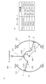
- Radius Ri It is a figure explaining the phase shift amount of the phase shifter in case radius Ro is 1: 3.
- (A) shows the equivalent circuit of a phase shifter
- (b) is a figure which shows phase shift amount. It is a figure which shows the connection relation of an array antenna and a phase shifter.
- Radius Ri It is a figure explaining the phase shift amount of the phase shifter in case radius Ro is 1: 2.
- (A) shows the equivalent circuit of the phase shifter 200
- (b) is a figure which shows phase shift amount. It is a figure which shows the inside of the phase shifter in 2nd Embodiment. It is a figure explaining an example of the composition of the omni antenna in a 3rd embodiment.
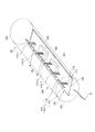
- FIG. 1 is a view showing an example of the entire configuration of a base station antenna 1 for mobile communication to which the first embodiment is applied.
- FIG. 1A is a perspective view of the base station antenna 1
- FIG. 1B is a view for explaining an installation example of the base station antenna 1.
- the base station antenna 1 includes, for example, a plurality of sector antennas 10-1 to 10-3 held by a steel tower 20, as shown in FIG. 1 (a). Then, as shown in FIG. 1 (b), the base station antenna 1 causes radio waves to reach the inside of the cell 2. That is, the cell 2 is a range where radio waves reach from the base station antenna 1.
- Each of the sector antennas 10-1 to 10-3 has a cylindrical outer shape, and a central axis of the cylinder is provided perpendicular to the ground.
- the cell 2 is provided with a plurality of sectors 3-1 to 3-3 which are divided at an angle in the horizontal plane.
- the sectors 3-1 to 3-3 are provided corresponding to the three sector antennas 10-1 to 10-3 of the base station antenna 1, respectively. That is, the direction of the main lobe 11 in which the electric field of the output radio waves of the sector antennas 10-1 to 10-3 is large is directed to the corresponding sectors 3-1 to 3-3.
- the sector antennas 10-1 to 10-3 are not distinguished from one another, they are referred to as a sector antenna 10.
- sectors 3-1 to 3-3 are not distinguished from one another, they are referred to as sector 3.
- the base station antenna 1 shown as an example in FIG. 1 includes three sector antennas 10-1 to 10-3, each of which corresponds to the sectors 3-1 to 3-3. And sectors 3 may be a predetermined number other than three. Further, in FIG. 1A, the sector 3 is configured by dividing the cell 2 into equal parts, but the division may not be equal and any one sector 3 is wider than the other sectors 3 or It may be narrowly configured.
- the base station antenna 1 mainly transmits radio waves, but due to the reversibility of the antenna, the base station antenna 1 receives radio waves.
- a transmission signal may be used as a reception signal and the flow of the signal may be reversed.
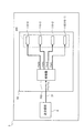
- Each sector antenna 10 includes an array antenna 100, a phase shifter 200, and a distributor 300.
- the sector antenna 10 may be described as an antenna.
- the phase shifter 200 has, for example, at least two input / output terminals (refer to Port 1 to Port 4 shown in FIG. 3 described later) as to phases of transmission signals input to the input / output terminals (refer to P-In / Out shown in FIG. Shifted and output differently.
- the distributor 300 matches a plurality of input / output terminals (for example, by matching impedances of transmission signals for transmitting radio waves input to input / output terminals (see D-In / Out 1 shown in FIG. 3 described later)). It distributes (outputs) to D-In / Out 2 and Port 0 shown in FIG. 3 described later.
- Each sector antenna 10 is connected to a transmission / reception cable 31 for transmitting a transmission signal to the distributor 300 and a reception signal from the distributor 300.
- the transmission / reception cable 31 is connected to a transmission / reception unit 4 (see FIG. 3 described later) which transmits a transmission signal and receives a reception signal provided in a base station (not shown).
- the transmission and reception cable 31 is, for example, a coaxial cable.
- the array antenna 100, the phase shifter 200, the distributor 300, and the transmission / reception cable 31 are described in the sector antenna 10-1. Similar to the sector antenna 10-1, the other sector antennas 10-2 to 10-3 also include the array antenna 100, the phase shifter 200, the distributor 300, and the transmission / reception cable 31, but these are not shown. ing. The array antenna 100, the phase shifter 200, and the distributor 300 will be described later.
- the base station antenna 1 preferably transmits radio waves into the cell 2 and does not transmit radio waves to cells adjacent to the outside of the cell 2. Similarly, it is preferable to receive radio waves from within the cell 2 and not to receive radio waves from cells adjacent to the outside of the cell 2. Therefore, as shown in FIG. 1A, the transmission direction and the reception direction (directivity) of radio waves (beams) are inclined by ⁇ from the horizontal plane to the ground direction (as a beam tilt angle ⁇ ).
- FIG. 2 is a diagram showing an example of the configuration of the sector antenna 10 in the first embodiment.
- FIG. 2 is a perspective view in which one sector antenna 10 is placed sideways.
- the sector antenna 10 includes a reflector 120, an array antenna 100 including a plurality of antenna elements arranged on the reflector 120, a phase shifter 200, a distributor 300, and a radome 500.
- the radome 500 is provided to wrap the array antenna 100, the reflector 120, the phase shifter 200, and the distributor 300.
- the radome 500 is shown by a broken line so that the array antenna 100 and the like provided inside the radome 500 can be seen.
- the phase shifter 200 and the distributor 300 are placed on the back surface of the reflecting plate 120, they are shown by broken lines.
- Array antenna 100 includes dipole antennas 110-1 to 110-5.
- dipole antennas 110-1 to 110-5 are not distinguished from one another, they are described as the dipole antenna 110.
- Each dipole antenna 110 is provided with the linear element parts 111 and 112 arranged on a straight line. Then, in a portion where the element portion 111 and the element portion 112 of the dipole antenna 110 face each other, one end is connected to the element portion 111 and the other end is similarly connected to the conductor portion 113 connected to the reflecting plate 120 described later.
- a conductor portion 114 connected to the element portion 112 and having the other end connected to the reflection plate 120 is provided.
- the element portions 111 and 112 and the conductor portions 113 and 114 are made of a conductor such as copper or aluminum on the surface side of an insulator substrate (not shown) such as epoxy resin.
- the dipole antenna 110 shown in FIG. 2 can transmit and receive polarization (vertical polarization) in which the electric field oscillates in a direction perpendicular to the ground surface.
- polarization horizontal polarization
- the dipole antenna 110 for receiving vertically polarized waves and the dipole antenna for receiving horizontally polarized waves are arranged alternately or in cross, so that the array antenna 100 transmits and receives both vertically polarized waves and horizontally polarized waves. May be
- the reflecting plate 120 reflects the radio wave transmitted by the dipole antenna 110 and holds the dipole antenna 110.
- five dipole antennas 110 are arranged on the reflector 120 at an interval Dp.
- the portion of the reflector 120 facing the dipole antenna 110 is flat, and both ends of the reflector 120 are bent to the opposite side to the side where the dipole antenna 110 is provided. In addition, the both ends do not need to be bent and may be bent to the side where the dipole antenna 110 is provided.
- the reflecting plate 120 is made of a conductor such as aluminum or copper.
- the reflecting plate 120 is provided commonly to the five dipole antennas 110-1 to 110-5, but may be considered to be separated for each dipole antenna 110.
- the radome 500 includes a cylinder 501, an upper lid 502 covering the upper end of the cylinder 501, and a lower lid 503 covering the lower end of the cylinder 501.
- the radome 500 stores the array antenna 100, the phase shifter 200, and the distributor 300 inside.
- the lower cover 503 of the radome 500 is provided with a connector (not shown) to which the distributor 300 and a transmission / reception cable 31 for transmitting transmission and reception signals are connected.
- the radome 500 is made of, for example, an insulating resin such as FRP (fiber reinforced plastics).
- the array antenna 100 of the sector antenna 10 shown in FIG. 2 is configured of five dipole antennas 110, the number of dipole antennas 110 is not limited to five, and may be a predetermined number.
- the sector antenna 10 shown in FIG. 2 is configured of one array antenna 100 including five dipole antennas 110, the sector antenna 10 may be configured by arranging a plurality of array antennas 100.
- the radome 500 covering the array antenna 100 and the like is a cylinder 501 provided with the upper cover 502 and the lower cover 503, but it may be a cylinder having a square cross section. It may be done.
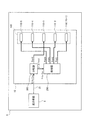
- FIG. 3 is a diagram showing the connection relationship of the array antenna 100, the phase shifter 200, and the distributor 300. As shown in FIG. Here, the array antenna 100 will be described as including five dipole antennas 110 (110-1, 110-2,..., 110-5).
- the phase shifter 200 is provided with five input / output terminals P-In / Out, Port 1 to Port 4. Each of Port 1 to Port 4 is an example of a first input / output terminal, and P-In / Out is an example of a second input / output terminal.
- the P-In / Out of the phase shifter 200 is connected to D-In / Out 2 which is an input / output terminal of a splitter 300 described later.
- Port 1 is connected to a dipole antenna 110-1, Port 2 to a dipole antenna 110-2, Port 3 to a dipole antenna 110-4, and Port 4 to a dipole antenna 110-5. As described later, the dipole antenna 110-3 is connected to Port 0 of the distributor 300 and not connected to the phase shifter 200.
- the Port 1 to Port 4 of the phase shifter 200 shift the phases of the transmission signals input to P-In / Out, and output the signals. Further, when the array antenna 100 receives a radio wave, P-In / Out shifts and combines the phases of the reception signals respectively input to Port 1 to Port 4 and outputs the result.
- the amount of phase shift (the amount of phase shift) can be varied by the rotation shaft 220 (see FIG. 4) provided in the phase shifter 200.
- the distributor 300 includes input / output terminals D-In / Out1, D-In / Out2, and Port0.
- the D-In / Out 1 of the distributor 300 is connected to the transmission / reception unit 4 via the transmission / reception cable 31.
- Port 0 of the distributor 300 is connected to the dipole antenna 110-3, and D-In / Out 2 is connected to P-In / Out of the phase shifter 200.
- the distributor 300 transmits the Port 0 and D-In in a state where the transmission signal input from the transmitting / receiving unit 4 to the D-In / Out 1 via the transmission / reception cable 31 is matched in impedance. It distributes to / Out2 and outputs.
- the reception signals input to Port 0 and D-In / Out 2 of the distributor 300 are combined and output from D-In / Out 1 to the transmission / reception unit 4 via the transmission / reception cable 31. Do.
- phase shifter 200 and the divider 300 operations of the phase shifter 200 and the divider 300 will be described.
- the case where radio waves are transmitted from the sector antenna 10 will be described. Due to the reversibility of the antenna, when the sector antenna 10 receives a radio wave, the signal flow direction may be reversed.
- the transmission signal transmitted from the transmission / reception unit 4 is input to D-In / Out 1 of the distributor 300 via the transmission / reception cable 31. Then, the transmission signal is distributed at the distributor 300 and output from D-In / Out 2, Port 0. Then, the transmission signal output from Port 0 is input to the dipole antenna 110-3, and the transmission signal output from D-In / Out 2 is input to P-In / Out of the phase shifter 200.
- the phase shift amount is “0”.
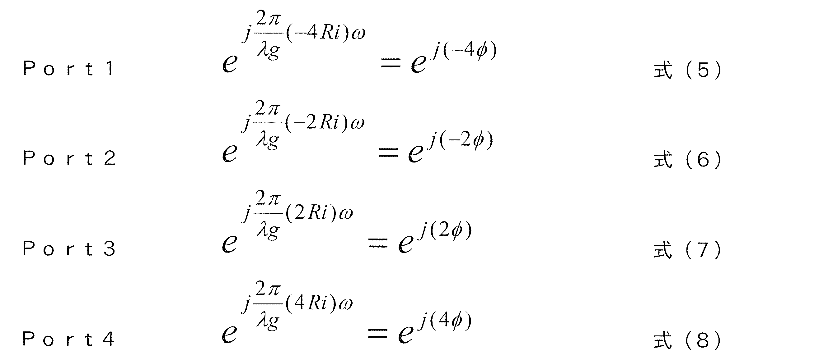
- Port 1 has a phase shift amount -4 ⁇
- Port 2 has a phase shift amount-2 ⁇
- Port 3 has a phase shift amount + 2 ⁇
- Port 4 has A transmission signal with a phase shift amount of + 4 ⁇ is output.
- ⁇ is a preset phase shift amount.
- Port 1 is connected to a dipole antenna 110-1, Port 2 to a dipole antenna 110-2, Port 3 to a dipole antenna 110-4, and Port 4 to a dipole antenna 110-5. Therefore, the transmission signals transmitted to the dipole antennas 110-1 to 110-5, including the dipole antenna 110-3 connected to Port 0 of the distributor 300, have phase shifts -4 ⁇ , -2 ⁇ , 0, + 2 ⁇ , respectively. It becomes + 4 ⁇ . That is, the difference in the phase shift amount of the transmission signal transmitted to each of the dipole antennas 110 is 2 ⁇ .
- the dipole antennas 110-1 to 110-5 are arranged at a constant interval Dp. Therefore, since the phase shift amount difference is 2 ⁇ , the directivity (beam tilt angle ⁇ in FIG. 1) of the output radio wave can be obtained from the interval Dp and 2 ⁇ which is the phase shift amount difference. That is, when the array antenna 100 is composed of a plurality of dipole antennas 110 arranged at a constant interval Dp, the directivity of the array antenna 100 is determined by the phase shift of the transmission signal transmitted to the dipole antennas 110 adjacent to each other. Control can be performed by setting the difference to be a predetermined value.
- the sector antenna 10 includes at least the array antenna 100 and the phase shifter 200.
- the wireless device 6 includes at least the sector antenna 10 and the transmitting / receiving unit 4.
- ports 1 to 4 of phase shifter 200 and port 0 of distributor 300 are connected to one dipole antenna 110, respectively.
- the ports 1 to 4 of the phase shifter 200 and the port 0 of the distributor 300 may be connected to a group including a plurality of dipole antennas 110, respectively.
- the dipole antennas 110-1 to 110-5 may be replaced with a group of dipole antennas 110, respectively.
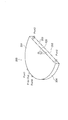
- FIG. 4 is a diagram showing an overview of the phase shifter 200 in the first embodiment.
- the phase shifter 200 includes, for example, both semicircular plate members 201 and 202.
- the plate members 201 and 202 are separated by a predetermined distance.
- the phase shifter 200 includes the side member 203 connected to each other in the linear portion of the plate members 201 and 202, and the side member 204 connected to each other in the semicircular arc portion of the plate members 201 and 202.
- the plate-like member 201 is an example of a first plate-like member
- the plate-like member 202 is an example of a second plate-like member.
- the phase shifter 200 is provided with Port 2 and Port 3 on the side member 203, and P-In / Out, Port 1 and Port 4 on the side member 204.
- P-In / Out, Port1, Port2, Port3, and Port4 are provided on the side surface member 203 and the side surface member 204, but part or all of these may be provided on the plate-like members 201 and 202.
- the plate members 201 and 202 and the side members 203 and 204 of the phase shifter 200 are made of a conductive material such as copper and aluminum.
- the plate-like members 201 and 202 and the side members 203 and 204 of the phase shifter 200 are at the same potential.
- interval of the plate-shaped members 201 and 202 is 10 mm, for example.
- phase shifter 200 further includes a rotating shaft 220 provided so as to protrude from a hole provided in the plate-like member 201.
- the plate-like members 201 and 202 of the phase shifter 200 have a semicircular shape, they may be square or may have another shape.
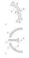
- FIG. 5 is a view showing the inside of the phase shifter 200 in the first embodiment.
- FIG. 5 (a) is a diagram showing the phase shifter 200 in a state in which the plate member 201 is removed
- FIG. 5 (b) is a diagram showing a cross section along the line VB-VB in FIG. 5 (a). is there.
- the phase shifter 200 has a straight conductor 211 and an arc-shaped conductor with a radius Ro as an example of a first radius of curvature inside the plate members 201 and 202 and the side members 203 and 204. 212, 213, a curved portion 214a curved in an arc shape having a radius Ri as an example of a second radius of curvature, and a conductor 214 provided with extending portions 214b, 214c extending linearly from both ends of the curved portion 214a, Is equipped.
- the radius Ro is the distance from the center (rotational axis 220) to the center of the width of each of the conductors 212 and 213.
- the radius Ri is the distance from the center (rotational axis 220) to the center of the width of the curved portion 214a of the conductor 214. That is, the conductors 212 and 213 and the curved portion 214a of the conductor 214 form part of concentric circles having the same center (rotational axis 220).
- the conductor 212 is an example of a first conductor
- the conductor 214 is an example of a second conductor
- the conductor 211 is an example of a third conductor.
- These conductors 211, 212, 213, 214 are made of a conductive material having high conductivity such as copper or aluminum, and have a width of 10 mm and a thickness of 1 mm, for example.
- the arc-shaped conductors 212 and 213 of radius Ro have, for example, a central angle of 80 ° and a radius Ro of, for example, 75 mm.
- the curved portion 214a of the conductor 214 which is curved in an arc shape of the radius Ri has a central angle of, for example, 100 °, and the radius Ri of, for example, 25 mm.
- radius Ri radius Ro is set to 1: 3.
- the arc-shaped conductors 212 and 213 having a radius Ro are provided so as not to overlap with each other, and a linear conductor 211 is provided between the conductors 212 and 213.
- the straight conductors 211 are provided in the radial direction of the circle of radius Ro.
- the conductor 211 does not overlap with the center (rotation shaft 220).
- the conductor 214 is adapted to rotate relative to the conductors 211, 212, 213 around the center (rotational axis 220). Since the conductor 214 does not overlap (do not intersect) the rotation shaft 220, the conductor 214 is fixed to the rotation shaft 220 by a holding member 221 which is an insulating material (dielectric material) that electrically insulates.
- One end of the linear conductor 211 is connected to P-In / Out, and the other end overlaps (crosses) the curved portion 214 a of the conductor 214.
- the other end of the conductor 211 extends in the width direction at a portion ⁇ overlapping the curved portion 214 a of the conductor 214 (see FIG. 6A described later).
- the spacer 231 which is a dielectric layer, is sandwiched in a portion ⁇ where the conductor 211 and the curved portion 214a of the conductor 214 overlap. That is, in the portion ⁇ where the conductor 211 and the curved portion 214 a of the conductor 214 overlap, the conductor 211 and the conductor 214 are capacitively coupled via the spacer 231.
- One end of the arc-shaped conductor 212 having a radius Ro is connected to Port 1 and the other end is connected to Port 3.
- One end of the arc-shaped conductor 213 of radius Ro is connected to Port 2 and the other end is connected to Port 4.
- the respective end portions of the extending portions 214b and 214c linearly extended from the both end portions of the curved portion 214a of the conductor 214 respectively overlap (cross) the conductors 212 and 213.
- the end of the extension 214 b extends in the width direction.
- a spacer 232 which is a dielectric layer is sandwiched in a portion ⁇ where the extension portion 214 b of the conductor 214 and the conductor 212 overlap.
- the conductor 214 and the conductor 212 are capacitively coupled to each other through the spacer 232 at a portion ⁇ where the extension 214 b of the conductor 214 and the conductor 212 overlap.
- the end of the extension 214 c extends in the width direction.
- a spacer 233 which is a dielectric layer, is interposed in a portion ⁇ where the extension portion 214c of the conductor 214 and the conductor 213 overlap.
- the conductor 214 and the conductor 213 are capacitively coupled to each other through the spacer 233 at a portion ⁇ where the extension 214 c of the conductor 214 and the conductor 213 overlap.
- the spacers 231, 232, and 233 are made of, for example, an insulating material (dielectric material) having a small loss at high frequencies, such as polytetrafluoroethylene. And when rotating the conductor 214, the spacers 231, 232, 233 reduce friction with the conductors 211, 212, 213 and facilitate sliding. Note that, instead of the spacers 231, 232, and 233 which are dielectric layers, an air layer may be used.
- the conductors 211, 212, and 213 may be rotated. It is only required that the conductor 214 and the conductors 211, 212, and 213 be relatively movable.
- the cross section shown in FIG. 5B is a cross section taken along the line VB-VB in FIG. 5A and shows the cross section of the conductor 214 (the extending portion 214c) and the cross section of the conductor 211.
- the conductors 211, 213 and 214 are sandwiched between the plate-like members 201 and 202 made of a conductive material.
- the conductor 212 is similar.
- the plate members 201 and 202 are at the same potential. That is, the conductors 211, 212, 213, and 214 and the plate-like members 201 and 202 form a triplate line structure.
- the phase shifter 200 is an electromagnetic protection type that is less susceptible to electromagnetic noise, and is easy to handle.
- the spacers 231, 232, and 233 which are dielectric layers, intervene in the portions where the conductors 211, 212, 213, and 214 overlap.
- the conductors 211, 212, 213, 214 are not configured on a substrate using an insulating material (dielectric material) such as glass epoxy. That is, since the space surrounded by the plate members 201 and 202 and the side members 203 and 204 is air, the dielectric loss (tan ⁇ ) for high frequency which is a transmission / reception signal propagating through the conductors 211, 212, 213 and 214. Occurrence is suppressed.
- the conductors 211, 212, and 213 are fixed to the plate-like members 201 and 202 by providing a spacer (not shown).
- the conductor 214 is fixed to the rotating shaft 220 via the holding member 221 as described above.
- the rotation shaft 220 extends to the outside of the space surrounded by the plate members 201 and 202 and the side members 203 and 204 through holes provided in the plate member 201.
- the conductor 214 rotates around the rotating shaft 220, and the position of the overlapping portion ⁇ of the curved portion 214a of the conductor 214 and the conductor 211 moves along the curved portion 214a.
- the position of the overlapping portion ⁇ of the extension 214 b and the conductor 212 moves along the conductor 212, and the position of the overlapping portion ⁇ of the extension 214 c of the conductor 214 and the conductor 213 moves along the conductor 213.
- the phases (phase shift amounts) of the transmission and reception signals change in the ports 1, 2, 3, and 4.
- the distance moved along is set to have a predetermined ratio. That is, it is set by the radius Ri and the radius Ro.
- the conductors 211, 212, 213 and 214 are surfaces parallel to the plate-like members 201 and 202 except the overlapping portions ⁇ , ⁇ and ⁇ (the surface shown by the line AA in FIG. 5B) It is provided inside. Thereby, the fluctuation of the impedance which occurs when the conductor 214 is rotated around the rotation axis 220 is suppressed.
- FIG. 6 is a diagram showing the conductors 211, 212, 213, and 214 in the phase shifter 200.
- FIG. 6 (a) shows the fixed conductors 211, 212, 213 and
- FIG. 6 (b) shows the rotating conductor 214.
- FIG. 6A the linear conductor 211 and the arc-shaped conductors 212 and 213 having a radius Ro are disposed so as not to overlap with each other.
- the conductor 214 is composed of a curved portion 214a curved in an arc shape with a radius Ri and elongated portions 214b and 214c linearly drawn from both ends of the curved portion 214a.
- the phase shifter 200 in the first embodiment has a configuration that can be easily assembled, and is excellent in mass productivity.
- the angle formed by the extension 214 b of the conductor 214 and the extension 214 c is at the center of the conductor 212 (position between the end to which Port 1 is connected and the end to which Port 3 is connected). In some cases, the extension 214 c is preferably set to be at the center of the conductor 213 (a position between the end to which Port 2 is connected and the end to which Port 4 is connected). If the conductors 212 and 213 are symmetrical in the plane of FIG. 5, there is no difference in the phase shift amount of Port 1 to Port 4 in this state.
- FIG. 7 is a diagram for explaining the phase shift amount of the phase shifter 200 when the radius Ri: the radius Ro is 1: 3.
- FIG. 7 (a) shows an equivalent circuit of the phase shifter 200
- FIG. 7 (b) shows the amount of phase shift.
- radio waves are transmitted.
- FIG. 7A in order to facilitate understanding, the angle formed by the extension portion 214b and the extension portion 214c of the conductor 214 in the phase shifter 200 shown in FIG. 5 is 180 °. Therefore, the extension portion 214 b and the extension portion 214 c of the conductor 214 are on one straight line, and the conductor 212 and the conductor 213 are symmetrical with respect to the BB line.
- FIG. 7 shows an equivalent circuit of the phase shifter 200
- FIG. 7 (b) shows the amount of phase shift.
- the angle formed by the extension portion 214b and the extension portion 214c of the conductor 214 in the phase shifter 200 shown in FIG. 5 is 180 °. Therefore, the extension portion 214
- the angle ⁇ (radian) formed by the line BB and the extending portion 214b and the extending portion 214c of the conductor 214 is set to be positive in the clockwise direction. In the case of counterclockwise rotation, the angle ⁇ may be made negative.
- a path along which a transmission signal input to P-In / Out propagates to Port 1 to Port 4 will be described.
- the transmission signal input to P-In / Out propagates through the conductor 211 and is then input to the conductor 214 via the portion ⁇ where the conductor 211 and the curved portion 214a of the conductor 214 overlap.
- the transmission signal propagated in the right direction in FIG. 7A in the conductor 214 propagates in the extension 214 b of the conductor 214.
- the current is input to the conductor 212 via the portion ⁇ where the extension 214 b of the conductor 214 and the conductor 212 overlap.
- the transmission signal input to the conductor 212 propagates the conductor 212 upward in FIG. 7A and reaches Port 1.
- the transmission signal input to the conductor 212 propagates the conductor 212 downward in FIG. 7A and reaches Port 3.
- the transmission signal propagated in the left direction in FIG. 7A in the conductor 214 propagates in the extending portion 214 c of the conductor 214.
- the signal is input to the conductor 213 via the portion ⁇ where the extension 214 c of the conductor 214 and the conductor 213 overlap.
- the transmission signal input to the conductor 213 propagates the conductor 213 upward in FIG. 7A. And it reaches Port4.
- the transmission signal input to the conductor 213 propagates the conductor 213 downward in FIG. 7A. And, it reaches Port2.
- the phase delay due to this is 2 ⁇ ⁇ ( ⁇ ⁇ Ri) / ⁇ g. Furthermore, the transmitted signal propagates in the conductor 212 ( ⁇ ⁇ Ro) longer than the “reference”. The phase delay due to this is 2 ⁇ ⁇ ( ⁇ ⁇ Ro) / ⁇ g. Therefore, the transmission signal in Port 1 is expressed by Equation (1).
- ⁇ g is the wavelength of the transmission signal propagating on the conductors 211, 212, 213, 214 of the phase shifter 200.
- the transmission signal propagates shorter ( ⁇ ⁇ Ri) in the bending portion 214a than the “reference”.
- the phase lead by this becomes 2 ⁇ ⁇ ( ⁇ ⁇ Ri) / ⁇ g.
- the transmission signal propagates in the conductor 213 ( ⁇ ⁇ Ro) longer than the “reference”.
- the phase delay due to this is 2 ⁇ ⁇ ( ⁇ ⁇ Ro) / ⁇ g. Therefore, the transmission signal at Port 2 is expressed by Equation (2).
- the transmission signal propagates ( ⁇ ⁇ Ri) longer in the bending portion 214 a than in the reference case, and propagates shorter ( ⁇ ⁇ Ro) than the “reference” in the conductor 212. . Therefore, the transmission signal at Port 3 is expressed by equation (3). Further, for Port 4, the transmission signal propagates shorter ( ⁇ ⁇ Ri) in the bending portion 214a than the “reference”, and propagates shorter ( ⁇ ⁇ Ro) in the conductor 213 than the “reference”. . Therefore, the transmission signal at Port 4 is expressed by Equation (4).
- the transmission signal transmitted from the transmission / reception unit 4 is divided by the distributor 300 so that the transmission signal from the Port 0 of the distributor 300 has a phase shift amount “0”. And it is inserted between Port3.
- the difference in phase shift amount between adjacent ports is made to be 2 ⁇ .
- the difference in the amount of phase shift between adjacent dipole antennas 110 is set to a predetermined value.
- the beam tilt angle ⁇ of the sector antenna 10 can be controlled.
- the rotating shaft 220 is rotated, and a portion ⁇ where the conductor 211 and the curved portion 214a of the conductor 214 overlap, a portion ⁇ where the extension portion 214b of the conductor 214 and the conductor 212 overlap, an extension portion 214c of the conductor 214 and the conductor 213
- the rotating shaft 220 may be manually rotated or may be electrically rotated by providing a motor.
- FIG. 8 is a diagram showing the connection relationship of the array antenna 100 and the phase shifter 200.
- the array antenna 100 will be described as including four dipole antennas 110 (110-1, 110-2,..., 110-4).
- the phase shifter 200 includes P-In / Out and four ports 1 to 4. P-In / Out is connected to the transmission / reception unit 4.
- Port 1 is connected to a dipole antenna 110-1, Port 2 to a dipole antenna 110-2, Port 3 to a dipole antenna 110-3, and Port 4 to a dipole antenna 110-4. That is, the distributor 300 is not provided, and the transmission signal from the transmission / reception unit 4 is input to P-In / Out of the phase shifter 200.
- each of Ports 1 to 4 of the phase shifter 200 is connected to one dipole antenna 110.
- the ports 1 to 4 of the phase shifter 200 may be connected to a group including a plurality of dipole antennas 110, respectively.
- the dipole antennas 110-1 to 110-4 may be replaced with a group of dipole antennas 110, respectively.
- the phase shifter 200 has the same configuration as that shown in FIGS. 4 and 5. However, radius Ri: radius Ro is set to 1: 2.
- FIG. 9 is a diagram for explaining the phase shift amount of the phase shifter 200 when the radius Ri: the radius Ro is 1: 2.
- FIG. 9 (a) shows an equivalent circuit of the phase shifter 200
- FIG. 9 (b) shows the amount of phase shift.
- the equations (1) to (4) are represented by the equations (9) to (12), respectively.
- 2 ⁇ / ⁇ g ⁇ Ri ⁇ ⁇ ⁇ .
- the difference in the amount of phase shift between Port 1 and Port 2 and Port 3, and between Port 3 and Port 4 is 2 ⁇ .
- the beam tilt angle ⁇ of the sector antenna 10 can be controlled by setting the amount of phase shift between the adjacent dipole antennas 110 to a predetermined value for the array antenna 100 arranged at the distance Dp (see FIG. 2). .
- the divider 300 is provided by setting the radius Ri: the radius Ro, and the phases of the ports of the phase shifter 200 and the port 0 from the divider 300 are predetermined.
- the phase difference of each port of the phase shifter 200 can be set to be a predetermined difference without setting the distributor 300.
- the radius Ri: the radius Ro may not be a ratio by an integer, but may be a ratio including a decimal.
- the phase shifter 200 includes four ports 1, 2, 3, and 4.
- the phase shifter 200 by combining the phase shifter 200 and the divider 300, it is possible to transmit transmission signals with different phases to the five dipole antennas 110 or the five groups of dipole antennas 110.
- received signals of five dipole antennas 110 or five groups of dipole antennas 110 can be synthesized by changing their phases.
- the phase shifter 200 includes eight ports 1, 2, 3, 4, 5, 6, 7, 8. Therefore, by combining the phase shifter 200 and the divider 300, it is possible to transmit transmission signals with different phases to groups of up to nine dipole antennas 110 or dipole antennas 110. In addition, received signals of groups of up to nine dipole antennas 110 or dipole antennas 110 can be synthesized with different phases. Furthermore, it is possible to transmit transmission signals with different phases to the eight dipole antennas 110 or eight groups of dipole antennas 110 only with the phase shifter 200. Then, received signals of eight dipole antennas 110 or eight groups of dipole antennas 110 can be synthesized by changing the phase.
- the other configuration is the same as that of the first embodiment. Therefore, in the following, the same reference numerals are given to the same parts, the description is omitted, and the different parts will be described.
- FIG. 10 is a view showing the inside of the phase shifter 200 in the second embodiment. As in FIG. 5A, the plate member 201 is removed to show the inside of the phase shifter 200.
- the phase shifter 200 has an arc shape of a radius Re further outside each of the curved conductors 212 and 213 of the radius Ro of the phase shifter 200 in the first embodiment shown in FIG. 5A.
- curved conductors 241 and 242 are provided with curved conductors 241 and 242.
- the conductors 241 and 242 are fixed in the same manner as the conductors 212 and 213. Then, both ends of the conductor 241 are connected to Port 5 and Port 7 respectively, and both ends of the conductor 242 are connected to Port 6 and Port 8 respectively.
- the extending portions 214 b and 214 c of the conductor 214 are extended so as to overlap with the conductors 241 and 242, respectively.
- a spacer 234, which is a dielectric layer, is interposed in a portion ⁇ where the extension portion 214b of the conductor 214 and the conductor 241 overlap.
- a spacer 235, which is a dielectric layer is sandwiched in a portion ⁇ where the extension portion 214c of the conductor 214 and the conductor 242 overlap.
- An air layer may be used instead of the spacers 234 and 235 which are dielectric layers.
- the phase shifter 200 includes P-In / Out and Port 1 to Port 8 as input / output terminals.
- Each of Port 1 to Port 8 is an example of a first input / output terminal
- P-In / Out is an example of a second input / output terminal.
- transmission signals input to P-In / Out of the phase shifter 200 can be output as transmission signals with different phase shifts from the eight ports 1 to 8.
- the phase shifts of the received signals input to the eight ports 1 to 8 can be changed and synthesized, and output from P-In / Out.
- Port 1 to Port 8 of the phase shifter 200 and Port 0 of the divider 300 according to the setting of the radius Ri, Ro, Re, predetermined phase shift amounts for groups of up to nine dipole antennas 110 or dipole antennas 110 Can be transmitted. Further, by setting the radius Ri, Ro, Re, it is possible to transmit a transmission signal having a predetermined difference in phase shift amount to eight dipole antennas 110 or eight groups of dipole antennas 110 only with phase shifter 200. . Also, the difference in phase shift amount between the ports includes the length (central angle) of each of the conductors 212, 213, 241, 242, the length (central angle) of the curved portion 214a of the conductor 214, the wavelength of radio waves to be transmitted and received, etc. It should be set by.
- the number of ports can be further increased by further adding a curved conductor to the outside of the conductors 241 and 242 of the phase shifter 200.
- the base station antenna 1 in the first embodiment and the second embodiment includes the plurality of sector antennas 10 (10-1 to 10-3) having directivity.
- the base station antenna 1 in the third embodiment includes an omnidirectional omni antenna 50.
- the base station antenna 1 in the third embodiment may include one omni antenna 50 or may include a plurality of omni antennas 50.
- the other configuration is the same as that of the first embodiment. Therefore, in the following, the same reference numerals are given to the same parts, the description is omitted, and the different parts will be described.
- FIG. 11 is a diagram for explaining an example of the configuration of the omni antenna 50 in the third embodiment.
- FIG. 10 is a perspective view in which one omni antenna 50 is placed sideways.
- the omni antenna 50 is provided so as to wrap the array antenna 150 including a plurality of antenna elements arranged at intervals Dp, the phase shifter 200, the distributor 300, the array antenna 150, the phase shifter 200, and the distributor 300.
- the radome 500 In FIG. 11, the radome 500 is shown by a broken line so that the array antenna 150 provided inside the radome 500 can be seen.
- Array antenna 150 includes dipole antennas 160-1 to 160-5.
- dipole antennas 160-1 to 160-5 are not distinguished from one another, they are described as the dipole antenna 160.
- Each dipole antenna 160 includes linear element portions 161 and 162 arranged in a straight line. And the part which the element part 161 and the element part 162 oppose becomes a feed point.
- the element portions 161 and 162 are made of a conductor such as copper or aluminum on the surface side of an insulator substrate (not shown) such as epoxy resin, for example.
- the dipole antenna 160 shown in FIG. 11 can transmit and receive polarization (vertical polarization) in which the electric field oscillates in a direction perpendicular to the ground surface. And, unlike the array antenna 100 shown in FIG. 2 in the first embodiment, the array antenna 150 does not include the reflector 120. Thus, the array antenna 150 can transmit and receive radio waves at 360 ° in the horizontal plane.
- the omni antenna 50 provided with four dipole antennas 160-1, 160-2, 160-3, and 160-4 is shown in FIG.
- the difference in phase shift amount between the adjacent dipole antennas 160 can be set to a predetermined value. .
- the beam tilt angle ⁇ of the omni antenna 50 can be controlled.
- the radius Ri: the radius Ro may not be a ratio by an integer, and may be a ratio including a decimal.
- the sector antenna 10 is configured by an antenna element (dipole antenna 110) that configures a dipole, even if it is configured using another antenna element different from a dipole Good.
- the omni antenna 50 is configured of an antenna element (dipole antenna 160) that configures a dipole, but may be configured using another antenna element different from a dipole.
- DESCRIPTION OF SYMBOLS 1 Base station antenna, 2 ... Cell, 3, 3-1 to 3-3 ... Sector, 4 ... Transmission / reception part, 6 ... Radio
Landscapes
- Engineering & Computer Science (AREA)
- Computer Networks & Wireless Communication (AREA)
- Variable-Direction Aerials And Aerial Arrays (AREA)
- Waveguide Switches, Polarizers, And Phase Shifters (AREA)
Abstract
Description
このような移相器において、第1の導体と第2の導体の延伸部とが電気的に結合する位置が第1の導体において移動する距離と、第2の導体の湾曲部と第3の導体とが電気的に結合する位置が第2の導体の湾曲部において移動する距離とは、予め定められた比に設定されることを特徴とすることができる。
また、第1の曲率半径及び第2の曲率半径は、共通の中心に対することを特徴とすることができる。
さらに、それぞれが導電材料で構成された第1の板状部材と第2の板状部材とをさらに備え、第1の導体、第2の導体及び第3の導体は、第1の板状部材と第2の板状部材との間に設けられていることを特徴とすることができる。
さらにまた、第1の導体と第2の導体の延伸部との電気的な結合又は第2の導体の湾曲部と第3の導体との電気的な結合は、誘電体層又は空気層を介在させた容量結合であることを特徴とすることができる。
このようなアンテナにおいて、第2の入出力端子に接続され、送受信信号を分配する分配器をさらに備えることを特徴とすることができる。
[第1の実施の形態]
<基地局アンテナ1>
図1は、第1の実施の形態が適用される移動通信用の基地局アンテナ1の全体構成の一例を示す図である。図1(a)は、基地局アンテナ1の斜視図であり、図1(b)は、基地局アンテナ1の設置例を説明する図である。
基地局アンテナ1は、例えば、図1(a)に示すように、鉄塔20に保持された複数のセクタアンテナ10-1~10-3を備えている。そして、図1(b)に示すように、基地局アンテナ1は、セル2内に電波を到達させる。すなわち、セル2は、基地局アンテナ1から電波が到達する範囲である。
セクタアンテナ10-1~10-3は、それぞれの外形が円筒状であって、円筒の中心軸が地面に対して垂直に設けられている。
なお、図1に例として示した基地局アンテナ1は、3個のセクタアンテナ10-1~10-3を備え、それぞれがセクタ3-1~3-3に対応しているが、セクタアンテナ10及びセクタ3は、3以外の予め定められた数であってもよい。また、図1(a)では、セクタ3は、セル2を等分に分割して構成されているが、等分でなくともよく、いずれか1つのセクタ3が他のセクタ3に比べ広く又は狭く構成されていてもよい。
移相器200は、例えば入出力端子(後述する図3に示すP-In/Out参照)に入力された送信信号の位相を少なくとも2つの入出力端子(後述する図3に示すPort1~Port4参照)間で異なるようにずらして出力する。
分配器300は、例えば入出力端子(後述する図3に示すD-In/Out1参照)に入力された、電波を送信するための送信信号を、インピーダンスをマッチングさせて、複数の入出力端子(後述する図3のD-In/Out2及びPort0参照)に分配(出力)する。
送受信ケーブル31は、基地局(不図示)内に設けられた送信信号を送信及び受信信号を受信する送受信部4(後述する図3参照)に接続されている。送受信ケーブル31は、例えば同軸ケーブルである。
なお、アレイアンテナ100、移相器200、分配器300については後述する。
このため、図1(a)に示すように、電波(ビーム)の送信方向及び受信方向(指向性)を水平面から地表方向に角度θ傾けて(ビーム・チルト角θとして)いる。
図2は、第1の実施の形態におけるセクタアンテナ10の構成の一例を示す図である。図2は、1つのセクタアンテナ10を横に置いた斜視図で示している。
セクタアンテナ10は、反射板120と、反射板120上に配列された複数のアンテナ素子を備えたアレイアンテナ100と、移相器200と、分配器300と、レドーム500とを備えている。なお、レドーム500は、アレイアンテナ100、反射板120、移相器200、分配器300を包むように設けられている。図2では、レドーム500を破線で示し、レドーム500の内部に設けられたアレイアンテナ100等が見えるようにしている。また、移相器200、分配器300は、反射板120の裏面に置かれているので、破線で示している。
アレイアンテナ100は、ダイポールアンテナ110-1~110-5を備えている。ここでも、ダイポールアンテナ110-1~110-5をそれぞれ区別しないときは、ダイポールアンテナ110と表記する。
それぞれのダイポールアンテナ110は、一直線上に並べられた直線状の素子部111、112を備えている。
そして、ダイポールアンテナ110の素子部111と素子部112とが対向する部分において、一端が素子部111に接続され、他端が後述する反射板120に接続される導体部113と、同様に一端が素子部112に接続され、他端が反射板120に接続される導体部114とが設けられている。
素子部111、112及び導体部113、114は、例えばエポキシ樹脂などの絶縁体基板(不図示)の表面側に、銅、アルミニウムなどの導体で構成されている。
反射板120のダイポールアンテナ110に対向する部分は平坦で、反射板120の両端部は、ダイポールアンテナ110が設けられた側とは逆の側に折り曲げられている。なお、両端部は折り曲げられてなくともよく、ダイポールアンテナ110が設けられた側に折り曲げられていてもよい。
反射板120は、導体、例えばアルミニウム、銅などで構成されている。
そして、レドーム500の下蓋503に、分配器300と送信信号及び受信信号を伝送する送受信ケーブル31が接続されるコネクタ(不図示)が設けられている。
レドーム500は、例えばFRP(fiber reinforced plastics)などの絶縁性の樹脂で構成されている。
また、図2に示すセクタアンテナ10は、5個のダイポールアンテナ110を備えた1個のアレイアンテナ100から構成されているが、複数のアレイアンテナ100を並べることで構成されてもよい。
図3は、アレイアンテナ100、移相器200、分配器300の接続関係を示す図である。
ここでは、アレイアンテナ100が5個のダイポールアンテナ110(110-1、110-2、…、110-5)を備えているとして説明する。
移相器200のP-In/Outは、後述する分配器300の入出力端子であるD-In/Out2に接続されている。Port1はダイポールアンテナ110-1に、Port2はダイポールアンテナ110-2に、Port3はダイポールアンテナ110-4に、Port4はダイポールアンテナ110-5にそれぞれ接続されている。なお、後述するように、ダイポールアンテナ110-3は、分配器300のPort0に接続され、移相器200には接続されていない。
また、アレイアンテナ100が電波を受信する場合、P-In/Outは、Port1~Port4にそれぞれ入力された受信信号の位相をずらして合成して出力する。
なお、ずらす位相の量(移相量)は、移相器200に設けられた回転軸220(図4参照)により可変できるようになっている。
分配器300は、アレイアンテナ100が電波を送信する場合、送受信部4から送受信ケーブル31を介してD-In/Out1に入力した送信信号を、インピーダンスを整合させた状態で、Port0及びD-In/Out2に分配して出力する。
また、アレイアンテナ100が電波を受信する場合、分配器300のPort0及びD-In/Out2に入力した受信信号を合成して、D-In/Out1から送受信ケーブル31を介して送受信部4に出力する。
そして、Port0から出力された送信信号がダイポールアンテナ110-3に入力し、D-In/Out2から出力された送信信号が移相器200のP-In/Outに入力する。
ここで、Port0から出力される送信信号の位相を基準として、移相量“0”とする。
Port1はダイポールアンテナ110-1に、Port2はダイポールアンテナ110-2に、Port3はダイポールアンテナ110-4に、Port4はダイポールアンテナ110-5に接続されている。よって、分配器300のPort0に接続されたダイポールアンテナ110-3を含め、ダイポールアンテナ110-1~110-5に送信された送信信号は、それぞれ移相量-4φ、-2φ、0、+2φ、+4φとなる。すなわち、ダイポールアンテナ110のそれぞれに送信される送信信号の移相量の差は2φとなる。
すなわち、アレイアンテナ100が一定の間隔Dpで配列された複数のダイポールアンテナ110から構成されていると、アレイアンテナ100の指向性は、互いに隣接するダイポールアンテナ110に送信する送信信号の移相量の差を予め定められた値となるように設定することによって制御することができる。
次に移相器200について詳述する。
図4は、第1の実施の形態における移相器200の概観を示す図である。
移相器200は、例えばともに半円形の板状部材201、202を備えている。そして、板状部材201、202は、予め定められた間隔で隔てられている。そして、移相器200は、板状部材201、202の直線部分において、相互に接続する側面部材203と、板状部材201、202の半円形の円弧部分において、相互に接続する側面部材204とを備えている。ここで、板状部材201は第1の板状部材の一例であって、板状部材202は第2の板状部材の一例である。
そして、移相器200は、側面部材203にPort2、Port3を備え、側面部材204にP-In/Out、Port1、Port4を備えている。ここでは、P-In/Out、Port1、Port2、Port3、Port4を側面部材203及び側面部材204に設けたが、これらの一部又は全てを板状部材201、202に設けてもよい。
そして、移相器200の板状部材201、202、側面部材203、204は同電位になっている。
そして、板状部材201、202の間隔は、例えば10mmである。
なお、半径Roは、中心(回転軸220)から導体212及び導体213のそれぞれの幅の中央までの距離である。同様に、半径Riは、中心(回転軸220)から導体214の湾曲部214aの幅の中央までの距離である。すなわち、導体212、213及び導体214の湾曲部214aとは、それぞれが中心(回転軸220)を同じくする同心円の一部を構成する。
ここで、導体212は第1の導体の一例、導体214は第2の導体の一例、導体211は第3の導体の一例である。
半径Roの円弧状の導体212、213は、中心角が例えば80°であって、半径Roが例えば75mmである。また、導体214における半径Riの円弧状に湾曲した湾曲部214aは、中心角が例えば100°であって、半径Riが例えば25mmである。ここでは、例として半径Ri:半径Roを1:3に設定している。
一方、導体214は、中心(回転軸220)の回りで、導体211、212、213に対して回転するようになっている。なお、導体214は、回転軸220と重ならない(交差しない)ので、電気的に絶縁する絶縁材料(誘電材料)である保持部材221によって、回転軸220に固定されている。
すなわち、導体211と導体214の湾曲部214aとが重なる部分αでは、スペーサ231を介して、導体211と導体214とが容量結合するように構成されている。
導体214の延伸部214bと導体212とが重なる部分βにおいて、延伸部214bの端部は、幅方向に広がっている。また、導体214の延伸部214bと導体212とが重なる部分βには、誘電体層であるスペーサ232が挟み込まれている。これにより、導体214の延伸部214bと導体212とが重なる部分βにおいて、スペーサ232を介して、導体214と導体212とが容量結合するように構成されている。
同様に、導体214の延伸部214cと導体213とが重なる部分γにおいて、延伸部214cの端部は幅方向に広がっている。また、導体214の延伸部214cと導体213とが重なる部分γには、誘電体層であるスペーサ233が挟み込まれている。これにより、導体214の延伸部214cと導体213とが重なる部分γにおいて、スペーサ233を介して、導体214と導体213とが容量結合するように構成されている。
また、スペーサ231、232、233は、例えばポリテトラフルオロエチレンなどの高周波において損失が少ない絶縁材料(誘電材料)で構成されている。そして、スペーサ231、232、233は、導体214を回転させる場合に、導体211、212、213との摩擦を減らし、摺動を容易にする。
なお、誘電体層であるスペーサ231、232、233の代わりに、空気層であってもよい。
移相器200では、図5(b)に示すように、導体211、213、214が、導電材料で構成された板状部材201、202の間に挟まれている。図5(b)に示されないが、導体212も同様である。そして、板状部材201、202は同電位になっている。すなわち、導体211、212、213、214は、板状部材201、202とで、トリプレートライン構造をなしている。よって、移相器200は、電磁ノイズの影響を受けにくい電磁防護型であるとともに、取り扱いが容易である。
すなわち、板状部材201、202、側面部材203、204で囲まれた空間は空気であるので、導体211、212、213、214を伝搬する送受信信号である高周波に対して誘電損失(tanδ)の発生が抑制されている。
回転軸220を回転させることで、導体214が回転軸220の回りで回転し、導体214の湾曲部214aと導体211との重なる部分αの位置が湾曲部214aに沿って移動し、導体214の延伸部214bと導体212との重なる部分βの位置が導体212に沿って移動し、導体214の延伸部214cと導体213との重なる部分γの位置が導体213に沿って移動する。これにより、Port1、2、3、4において、送受信信号の位相(移相量)が変化する。
図6(a)に示すように、直線状の導体211と半径Roの円弧状に湾曲した導体212、213とはそれぞれが重ならないように配置されている。一方、図6(b)に示すように、導体214は、半径Riの円弧状に湾曲した湾曲部214aと、湾曲部214aの両端から直線状に延伸した延伸部214b、214cとから構成されている。
よって、第1の実施の形態における移相器200は、容易に組み立てられる構成を有し、量産性に優れている。
図7(a)では、理解を容易にするため、図5に示した移相器200における導体214の延伸部214bと延伸部214cとのなす角が180°になるように広げている。よって、導体214の延伸部214bと延伸部214cとが一つの直線上にあって、導体212と導体213とがB-B線に対して対称となる。そして、図7(a)では、B-B線と導体214の延伸部214b及び延伸部214cとのなす角度ω(ラジアン)を時計回りが正となるように設定している。
なお、反時計回りにある場合は、角度ωを負とすればよい。
P-In/Outに入力した送信信号は、導体211を伝搬した後、導体211と導体214の湾曲部214aとが重なる部分αを経由して、導体214に入力する。導体214を図7(a)において右方向に伝搬した送信信号は、導体214の延伸部214bを伝搬する。そして、導体214の延伸部214bと導体212とが重なる部分βを経由して、導体212に入力する。そして、導体212に入力した送信信号は、導体212を図7(a)において上方向に伝搬して、Port1に到達する。また、導体212に入力した送信信号は、導体212を図7(a)において下方向に伝搬して、Port3に到達する。
一方、導体214を図7(a)において左方向に伝搬した送信信号は、導体214の延伸部214cを伝搬する。そして、導体214の延伸部214cと導体213とが重なる部分γを経由して、導体213に入力する。そして、導体213に入力した送信信号は、導体213を図7(a)において上方向に伝搬する。そして、Port4に到達する。また、導体213に入力した送信信号は、導体213を図7(a)において下方向に伝搬する。そして、Port2に到達する。
まず、Port1を説明する。延伸部214bがB-B線に対して角度ωの位置にあるので、送信信号は、湾曲部214aにおいて、“基準”に比べて(ω×Ri)長く伝搬する。これによる位相の遅れは、2π×(ω×Ri)/λgとなる。さらに、送信信号は、導体212において、“基準”に比べて(ω×Ro)長く伝搬する。これによる位相の遅れは、2π×(ω×Ro)/λgとなる。よって、Port1における送信信号は式(1)で表される。
なお、λgは、移相器200の導体211、212、213、214上を伝搬する送信信号の波長である。
また、Port4に対しては、送信信号は、湾曲部214aにおいて、“基準”に比べて(ω×Ri)短く伝搬し、導体213において、“基準”に比べて(ω×Ro)短く伝搬する。よって、Port4におけるに送信信号は式(4)で表される。

これにより、5つのダイポールアンテナ110を等間隔(図2の間隔Dp参照)に並べたアレイアンテナ100に対し、隣接するダイポールアンテナ110間における移相量の差を予め定められた値に設定して、セクタアンテナ10のビーム・チルト角θを制御できる。
回転軸220は、手動によって回転させてもよく、モータを設けて電気的に回転させてもよい。モータで回転軸220を回転させる場合は、モータによる回転軸220の回転角を制御するために、セクタアンテナ10の外部に制御装置を設けて、制御信号を送信することで行ってもよい。
図5に示した移相器200において、半径Ri:半径Roを1:3と異なる値に設定することができる。
図8は、アレイアンテナ100、移相器200の接続関係を示す図である。
ここでは、アレイアンテナ100が4個のダイポールアンテナ110(110-1、110-2、…、110-4)を備えているとして説明する。
移相器200は、P-In/Outと4つのPort1~Port4とを備えている。P-In/Outは、送受信部4に接続されている。Port1はダイポールアンテナ110-1に、Port2はダイポールアンテナ110-2に、Port3はダイポールアンテナ110-3に、Port4はダイポールアンテナ110-4にそれぞれ接続されている。すなわち、分配器300を備えず、送受信部4からの送信信号は、移相器200のP-In/Outに入力される。
なお、図8において、移相器200のPort1~4は、それぞれが1つのダイポールアンテナ110に接続されている。しかし、移相器200のPort1~4が、それぞれ複数のダイポールアンテナ110を含んだグループに接続されてもよい。この場合は、図8において、ダイポールアンテナ110-1~110-4をそれぞれダイポールアンテナ110のグループに置き換えればよい。
そして、移相器200は、図4、図5に示したと同様の構成である。しかし、半径Ri:半径Ro=1:2に設定されている。
半径Ri:半径Ro=1:2の場合、式(1)~式(4)は、それぞれ式(9)~式(12)で表される。ここで、2π/λg・Ri・ω=φとしている。すると、Port1とPort2との間、Port2とPort3との間、Port3とPort4との間における移相量の差は、すべて2φである。

すなわち、Port1~Port4の送信信号を、4個のダイポールアンテナ110-1、110-2、110-3、110-4を備えるアレイアンテナ100に供給すれば、隣接する4つのダイポールアンテナ110を等間隔(図2の間隔Dp参照)に並べたアレイアンテナ100に対し、隣接するダイポールアンテナ110間における移相量を予め定められた値に設定して、セクタアンテナ10のビーム・チルト角θを制御できる。
なお、半径Ri:半径Roは、整数による比でなくともよく、小数を含んだ比であってもよい。
第1の実施の形態では、移相器200は4個のPort1、2、3、4を備えていた。この場合、移相器200と分配器300とを組み合わせることで、5個のダイポールアンテナ110又は5グループのダイポールアンテナ110に、それぞれ位相を変えた送信信号を送信できた。また、5個のダイポールアンテナ110又は5グループのダイポールアンテナ110の受信信号を、それぞれ位相を変えて合成できた。
さらに、移相器200のみで、4個のダイポールアンテナ110又は4グループのダイポールアンテナ110に、それぞれ位相を変えた送信信号を送信できた。そして、4個のダイポールアンテナ110又は4グループのダイポールアンテナ110の受信信号を、それぞれ位相を変えて合成できた。
さらに、移相器200のみで、8個のダイポールアンテナ110又は8グループのダイポールアンテナ110に、それぞれ位相を変えた送信信号を送信できる。そして、8個のダイポールアンテナ110又は8グループのダイポールアンテナ110の受信信号を、それぞれ位相を変えて合成できる。
他の構成は、第1の実施の形態と同様である。よって、以下では、同様の部分には同じ符号を付して説明を省略し、異なる部分を説明する。
図10は、第2の実施の形態における移相器200の内部を示す図である。図5(a)と同様に、板状部材201を除去して移相器200の内部を示している。
なお、誘電体層であるスペーサ234、235の代わりに、空気層であってもよい。
このようにすることで、移相器200のP-In/Outに入力した送信信号を、8個のPort1~8から、移相が異なる送信信号として出力させることができる。同様に、8個のPort1~8に入力した受信信号の移相を変えて合成して、P-In/Outから出力させることができる。
また、Port間の移相量の差は、導体212、213、241、242のそれぞれの長さ(中心角)、導体214の湾曲部214aの長さ(中心角)及び送受信する電波の波長などによって設定すればよい。
第1の実施の形態及び第2の実施の形態における基地局アンテナ1は、指向性を有する複数のセクタアンテナ10(10-1~10-3)を備えていた。第3の実施の形態における基地局アンテナ1は、無指向性のオムニアンテナ50を備えている。なお、第3の実施の形態における基地局アンテナ1は、一のオムニアンテナ50を備えてもよく、複数のオムニアンテナ50を備えてもよい。
他の構成は、第1の実施の形態と同様である。よって、以下では、同様の部分には同じ符号を付して説明を省略し、異なる部分を説明する。
図11は、第3の実施の形態におけるオムニアンテナ50の構成の一例を説明する図である。図10は、1つのオムニアンテナ50を横に置いた斜視図で示している。
オムニアンテナ50は、間隔Dpで並べられた複数のアンテナ素子を備えたアレイアンテナ150と、移相器200と、分配器300と、アレイアンテナ150、移相器200、分配器300を包むように設けられたレドーム500とを備えている。図11では、レドーム500を破線で示し、レドーム500の内部に設けられたアレイアンテナ150が見えるようにしている。
アレイアンテナ150は、ダイポールアンテナ160-1~160-5を備えている。ここでも、ダイポールアンテナ160-1~160-5をそれぞれ区別しないときは、ダイポールアンテナ160と表記する。
それぞれのダイポールアンテナ160は、一直線上に並べられた直線状の素子部161、162を備えている。
そして、素子部161と素子部162とが対向する部分が給電点となっている。
素子部161、162は、例えばエポキシ樹脂などの絶縁体基板(不図示)の表面側に、銅、アルミニウムなどの導体で構成されている。
そして、アレイアンテナ150は、第1の実施の形態における図2で示したアレイアンテナ100と異なって、反射板120を備えない。よって、アレイアンテナ150は、水平面内360°において、電波の送受信が可能となる。
また、半径Ri:半径Roは、整数による比でなくともよく、小数を含んだ比であってもよい。
第3の実施の形態では、オムニアンテナ50を、ダイポールを構成するアンテナ素子(ダイポールアンテナ160)で構成したが、ダイポールと異なる他のアンテナ素子を用いて構成してもよい。
Claims (8)
- 第1の曲率半径を有し、一端部が第1の入出力端子に接続され、導電材料で構成された第1の導体と、
前記第1の曲率半径より小さい第2の曲率半径の湾曲部と、当該湾曲部の一端部から前記第1の導体と電気的に結合するように延びた延伸部とを備え、当該第1の導体との電気的に結合する位置が、当該第1の導体において相対的に移動可能である、導電材料で構成された第2の導体と、
一端部が第2の入出力端子に接続され、他端部が前記第2の導体の前記湾曲部と電気的に結合するように延びるとともに、当該第2の導体との電気的に結合する位置が当該湾曲部において相対的に移動可能である、導電材料で構成された第3の導体と
を備える移相器。 - 前記第1の導体と前記第2の導体の前記延伸部とが電気的に結合する位置が当該第1の導体において移動する距離と、当該第2の導体の前記湾曲部と前記第3の導体とが電気的に結合する位置が当該第2の導体の当該湾曲部において移動する距離とは、予め定められた比に設定されることを特徴とする請求項1に記載の移相器。
- 前記第1の曲率半径及び前記第2の曲率半径は、共通の中心に対することを特徴とする請求項1又は2に記載の移相器。
- それぞれが導電材料で構成された第1の板状部材と第2の板状部材とをさらに備え、前記第1の導体、前記第2の導体及び前記第3の導体は、当該第1の板状部材と当該第2の板状部材との間に設けられていることを特徴とする請求項1乃至3のいずれか1項に記載の移相器。
- 前記第1の導体と前記第2の導体の前記延伸部との電気的な結合又は当該第2の導体の前記湾曲部と前記第3の導体との電気的な結合は、誘電体層又は空気層を介在させた容量結合であることを特徴とする請求項1乃至4のいずれか1項に記載の移相器。
- 複数のアンテナ素子と、
第1の曲率半径を有し、一端部が第1の入出力端子と接続され、導電材料で構成された第1の導体と、当該第1の曲率半径より小さい第2の曲率半径の湾曲部と、当該湾曲部の一端部から当該第1の導体と電気的に結合するように延びた延伸部とを備え、当該第1の導体との電気的に結合する位置が、当該第1の導体において相対的に移動可能である、導電材料で構成された第2の導体と、一端部が第2の入出力端子に接続され、他端部が当該第2の導体の当該湾曲部と電気的に結合するように延びるとともに、当該第2の導体との電気的に結合する位置が当該湾曲部において相対的に移動可能である、導電材料で構成された第3の導体と、を備え、当該第1の入出力端子が前記複数のアンテナ素子のいずれかに接続される移相器と
を備えるアンテナ。 - 前記第2の入出力端子に接続され、送受信信号を分配する分配器をさらに備えることを特徴とする請求項6に記載のアンテナ。
- 複数のアンテナ素子と、
第1の曲率半径を有し、一端部が第1の入出力端子と接続され、導電材料で構成された第1の導体と、当該第1の曲率半径より小さい第2の曲率半径の湾曲部と、当該湾曲部の一端部から当該第1の導体と電気的に結合するように延びた延伸部とを備え、当該第1の導体との電気的に結合する位置が、当該第1の導体において相対的に移動可能である、導電材料で構成された第2の導体と、一端部が第2の入出力端子に接続され、他端部が当該第2の導体の当該湾曲部と電気的に結合するように延びるとともに、当該第2の導体との電気的に結合する位置が当該湾曲部において相対的に移動可能である、導電材料で構成された第3の導体と、を備え、当該第1の入出力端子が前記複数のアンテナ素子のいずれかに接続される移相器と、
前記複数のアンテナ素子において前記第1の入出力端子に接続されるアンテナ素子が電波を送信するための送信信号を前記第2の入出力端子に送信し、又は当該アンテナ素子が受信した電波から変換された受信信号を当該第2の入出力端子から受信する送受信部と
を備える無線装置。
Priority Applications (4)
| Application Number | Priority Date | Filing Date | Title |
|---|---|---|---|
| CN201480016448.0A CN105051971A (zh) | 2013-03-29 | 2014-03-18 | 移相器、天线以及无线装置 |
| US14/779,687 US20160049709A1 (en) | 2013-03-29 | 2014-03-18 | Phase shifter, antenna and radio apparatus |
| EP14775209.1A EP2980917A4 (en) | 2013-03-29 | 2014-03-18 | DEHASTER, ANTENNA AND RADIO DEVICE |
| PH12015502252A PH12015502252A1 (en) | 2013-03-29 | 2015-09-28 | Phase shifter, antenna and radio apparatus |
Applications Claiming Priority (2)
| Application Number | Priority Date | Filing Date | Title |
|---|---|---|---|
| JP2013071364A JP5677494B2 (ja) | 2013-03-29 | 2013-03-29 | 移相器、アンテナ及び無線装置 |
| JP2013-071364 | 2013-03-29 |
Publications (1)
| Publication Number | Publication Date |
|---|---|
| WO2014156841A1 true WO2014156841A1 (ja) | 2014-10-02 |
Family
ID=51623821
Family Applications (1)
| Application Number | Title | Priority Date | Filing Date |
|---|---|---|---|
| PCT/JP2014/057352 WO2014156841A1 (ja) | 2013-03-29 | 2014-03-18 | 移相器、アンテナ及び無線装置 |
Country Status (6)
| Country | Link |
|---|---|
| US (1) | US20160049709A1 (ja) |
| EP (1) | EP2980917A4 (ja) |
| JP (1) | JP5677494B2 (ja) |
| CN (1) | CN105051971A (ja) |
| PH (1) | PH12015502252A1 (ja) |
| WO (1) | WO2014156841A1 (ja) |
Cited By (2)
| Publication number | Priority date | Publication date | Assignee | Title |
|---|---|---|---|---|
| WO2017208382A1 (ja) * | 2016-06-01 | 2017-12-07 | 日本電業工作株式会社 | 移相器、分配/合成装置、アレイアンテナ及びセクタアンテナ |
| CN113363724A (zh) * | 2021-05-31 | 2021-09-07 | 武汉虹信科技发展有限责任公司 | 可切换波束的移相器及天线 |
Families Citing this family (9)
| Publication number | Priority date | Publication date | Assignee | Title |
|---|---|---|---|---|
| US10305198B2 (en) * | 2015-02-25 | 2019-05-28 | At&T Intellectual Property I, L.P. | Facilitating wireless communications via wireless communication assembly apparatuses |
| DE102015004658A1 (de) * | 2015-04-13 | 2016-10-13 | Kathrein-Werke Kg | Differenz-Phasenschieberbaugruppe |
| EP3096393B1 (de) * | 2015-05-22 | 2018-01-24 | Kathrein Werke KG | Differenz-phasenschieberbaugruppe |
| CN107046168A (zh) * | 2016-09-18 | 2017-08-15 | 北京邮电大学 | 一种微带天线 |
| KR101826892B1 (ko) | 2017-02-28 | 2018-02-08 | 주식회사 이엠따블유 | 위상 변위기 및 이를 포함하는 통신 장치 |
| CN109193161B (zh) * | 2018-08-27 | 2021-05-07 | 京信通信技术(广州)有限公司 | 移相器及天线 |
| CN110011005B (zh) * | 2019-05-10 | 2022-03-29 | 常州仁千电气科技股份有限公司 | 一种应用于圆极化天线的小型化功分移相器 |
| CN111525215B (zh) * | 2020-05-06 | 2021-11-16 | 湖南时变通讯科技有限公司 | 移相单元、天线单元、相控阵列单元以及相控阵列 |
| CN114927840A (zh) * | 2022-06-14 | 2022-08-19 | 昆山立讯射频科技有限公司 | 移相装置及基站天线 |
Citations (6)
| Publication number | Priority date | Publication date | Assignee | Title |
|---|---|---|---|---|
| JPH04320122A (ja) * | 1991-04-19 | 1992-11-10 | Nippon Telegr & Teleph Corp <Ntt> | アンテナビーム制御方式 |
| JPH0677710A (ja) * | 1992-08-26 | 1994-03-18 | Sumitomo Electric Ind Ltd | 可変移相4分配器 |
| JP2005506789A (ja) * | 2001-10-22 | 2005-03-03 | キネテイツク・リミテツド | アンテナシステムを向ける装置 |
| JP2008507163A (ja) * | 2004-06-04 | 2008-03-06 | アンドルー、コーパレイシャン | 指向性ダイポール・アンテナ |
| JP2009177808A (ja) * | 2008-01-25 | 2009-08-06 | Commscope Inc Of North Carolina | 位相シフタ及び位相シフタを含むアンテナ |
| JP2009542155A (ja) | 2006-06-26 | 2009-11-26 | ケーエムダブリュ・インコーポレーテッド | 可変移相器 |
Family Cites Families (6)
| Publication number | Priority date | Publication date | Assignee | Title |
|---|---|---|---|---|
| US4633203A (en) * | 1986-02-28 | 1986-12-30 | Motorola, Inc. | Combined microstripline phase shifter and electric field probe |
| US7233217B2 (en) * | 2001-08-23 | 2007-06-19 | Andrew Corporation | Microstrip phase shifter |
| KR100562534B1 (ko) * | 2003-07-14 | 2006-03-22 | 주식회사 에이스테크놀로지 | 전력 분배 기능을 구비한 위상 가변기 |
| CN101080848B (zh) * | 2004-06-04 | 2012-09-12 | 安德鲁公司 | 定向偶极子天线 |
| FR2930078B1 (fr) * | 2008-04-15 | 2011-08-26 | Alcatel Lucent | Dispositif de dephasage rotatif |
| JP4650561B2 (ja) * | 2008-12-02 | 2011-03-16 | 住友電気工業株式会社 | 移相器 |
-
2013
- 2013-03-29 JP JP2013071364A patent/JP5677494B2/ja not_active Expired - Fee Related
-
2014
- 2014-03-18 US US14/779,687 patent/US20160049709A1/en not_active Abandoned
- 2014-03-18 CN CN201480016448.0A patent/CN105051971A/zh active Pending
- 2014-03-18 WO PCT/JP2014/057352 patent/WO2014156841A1/ja active Application Filing
- 2014-03-18 EP EP14775209.1A patent/EP2980917A4/en not_active Withdrawn
-
2015
- 2015-09-28 PH PH12015502252A patent/PH12015502252A1/en unknown
Patent Citations (6)
| Publication number | Priority date | Publication date | Assignee | Title |
|---|---|---|---|---|
| JPH04320122A (ja) * | 1991-04-19 | 1992-11-10 | Nippon Telegr & Teleph Corp <Ntt> | アンテナビーム制御方式 |
| JPH0677710A (ja) * | 1992-08-26 | 1994-03-18 | Sumitomo Electric Ind Ltd | 可変移相4分配器 |
| JP2005506789A (ja) * | 2001-10-22 | 2005-03-03 | キネテイツク・リミテツド | アンテナシステムを向ける装置 |
| JP2008507163A (ja) * | 2004-06-04 | 2008-03-06 | アンドルー、コーパレイシャン | 指向性ダイポール・アンテナ |
| JP2009542155A (ja) | 2006-06-26 | 2009-11-26 | ケーエムダブリュ・インコーポレーテッド | 可変移相器 |
| JP2009177808A (ja) * | 2008-01-25 | 2009-08-06 | Commscope Inc Of North Carolina | 位相シフタ及び位相シフタを含むアンテナ |
Non-Patent Citations (1)
| Title |
|---|
| See also references of EP2980917A4 |
Cited By (4)
| Publication number | Priority date | Publication date | Assignee | Title |
|---|---|---|---|---|
| WO2017208382A1 (ja) * | 2016-06-01 | 2017-12-07 | 日本電業工作株式会社 | 移相器、分配/合成装置、アレイアンテナ及びセクタアンテナ |
| JPWO2017208382A1 (ja) * | 2016-06-01 | 2019-03-28 | 日本電業工作株式会社 | 移相器、分配/合成装置及びセクタアンテナ |
| CN112713368A (zh) * | 2016-06-01 | 2021-04-27 | 日本电业工作株式会社 | 分配/合成装置以及扇区天线 |
| CN113363724A (zh) * | 2021-05-31 | 2021-09-07 | 武汉虹信科技发展有限责任公司 | 可切换波束的移相器及天线 |
Also Published As
| Publication number | Publication date |
|---|---|
| PH12015502252A1 (en) | 2016-02-01 |
| JP2014195228A (ja) | 2014-10-09 |
| EP2980917A1 (en) | 2016-02-03 |
| US20160049709A1 (en) | 2016-02-18 |
| EP2980917A4 (en) | 2016-11-16 |
| JP5677494B2 (ja) | 2015-02-25 |
| CN105051971A (zh) | 2015-11-11 |
Similar Documents
| Publication | Publication Date | Title |
|---|---|---|
| WO2014156841A1 (ja) | 移相器、アンテナ及び無線装置 | |
| JP5518985B2 (ja) | 円偏波アンテナ | |
| US10148009B2 (en) | Sparse phase-mode planar feed for circular arrays | |
| CN104810577A (zh) | 一种基站电调天线宽频带慢波移相器 | |
| WO2014034490A1 (ja) | アンテナ | |
| WO2014115427A1 (ja) | アレイアンテナ | |
| EP3223369B1 (en) | Re-radiation repeater | |
| JP4528005B2 (ja) | ダイポール部材を備えているようなビーム幅調節可能型かつ方位角走査型アンテナ | |
| CN106602233A (zh) | 基于高低频复用的小型双圆极化天线 | |
| JP5620534B2 (ja) | 移相器及びアンテナシステム | |
| Zhang et al. | Low‐cost Ku‐band dual‐polarized and beam switchable cross‐type antenna array for satellite communications | |
| Roy et al. | A Comparative Analysis of UWB Phased Arrays With Combining Network for Wireless-Power-Transfer Applications | |
| US11855351B2 (en) | Base station antenna feed boards having RF transmission lines of different types for providing different transmission speeds | |
| WO2015159871A1 (ja) | アンテナ及びセクタアンテナ | |
| JP5877241B2 (ja) | 移相器、アンテナ及び無線装置 | |
| JP2016140046A (ja) | 偏波共用アンテナ | |
| JP5819485B1 (ja) | 分配移相器 | |
| CN113964536A (zh) | 一种圆极化两维宽角相扫天线单元及相控阵天线阵列 | |
| CN209200136U (zh) | 一种宽频带圆极化微带天线 | |
| WO2014115653A1 (ja) | アンテナ及びセクタアンテナ | |
| JP4498625B2 (ja) | ファンビームアンテナ | |
| Kubwimana et al. | Beam steering with 5.75 GHz dual polarized optically transparent patch antenna arrays | |
| WO2018179160A1 (ja) | アレイアンテナ及びセクタアンテナ | |
| Huang | Antenna Array Designs For Directional Wireless Communicatoin | |
| JP2001189619A (ja) | 平面アンテナ |
Legal Events
| Date | Code | Title | Description |
|---|---|---|---|
| WWE | Wipo information: entry into national phase |
Ref document number: 201480016448.0 Country of ref document: CN |
|
| 121 | Ep: the epo has been informed by wipo that ep was designated in this application |
Ref document number: 14775209 Country of ref document: EP Kind code of ref document: A1 |
|
| WWE | Wipo information: entry into national phase |
Ref document number: 14779687 Country of ref document: US |
|
| REEP | Request for entry into the european phase |
Ref document number: 2014775209 Country of ref document: EP |
|
| WWE | Wipo information: entry into national phase |
Ref document number: 12015502252 Country of ref document: PH Ref document number: 2014775209 Country of ref document: EP |
|
| NENP | Non-entry into the national phase |
Ref country code: DE |