WO2014156752A1 - 成膜装置 - Google Patents
成膜装置 Download PDFInfo
- Publication number
- WO2014156752A1 WO2014156752A1 PCT/JP2014/057086 JP2014057086W WO2014156752A1 WO 2014156752 A1 WO2014156752 A1 WO 2014156752A1 JP 2014057086 W JP2014057086 W JP 2014057086W WO 2014156752 A1 WO2014156752 A1 WO 2014156752A1
- Authority
- WO
- WIPO (PCT)
- Prior art keywords
- surface wave
- microwave
- negative voltage
- voltage application
- sheath layer
- Prior art date
- Legal status (The legal status is an assumption and is not a legal conclusion. Google has not performed a legal analysis and makes no representation as to the accuracy of the status listed.)
- Ceased
Links
Images





Classifications
-
- C—CHEMISTRY; METALLURGY
- C23—COATING METALLIC MATERIAL; COATING MATERIAL WITH METALLIC MATERIAL; CHEMICAL SURFACE TREATMENT; DIFFUSION TREATMENT OF METALLIC MATERIAL; COATING BY VACUUM EVAPORATION, BY SPUTTERING, BY ION IMPLANTATION OR BY CHEMICAL VAPOUR DEPOSITION, IN GENERAL; INHIBITING CORROSION OF METALLIC MATERIAL OR INCRUSTATION IN GENERAL
- C23C—COATING METALLIC MATERIAL; COATING MATERIAL WITH METALLIC MATERIAL; SURFACE TREATMENT OF METALLIC MATERIAL BY DIFFUSION INTO THE SURFACE, BY CHEMICAL CONVERSION OR SUBSTITUTION; COATING BY VACUUM EVAPORATION, BY SPUTTERING, BY ION IMPLANTATION OR BY CHEMICAL VAPOUR DEPOSITION, IN GENERAL
- C23C16/00—Chemical coating by decomposition of gaseous compounds, without leaving reaction products of surface material in the coating, i.e. chemical vapour deposition [CVD] processes
- C23C16/44—Chemical coating by decomposition of gaseous compounds, without leaving reaction products of surface material in the coating, i.e. chemical vapour deposition [CVD] processes characterised by the method of coating
- C23C16/50—Chemical coating by decomposition of gaseous compounds, without leaving reaction products of surface material in the coating, i.e. chemical vapour deposition [CVD] processes characterised by the method of coating using electric discharges
- C23C16/511—Chemical coating by decomposition of gaseous compounds, without leaving reaction products of surface material in the coating, i.e. chemical vapour deposition [CVD] processes characterised by the method of coating using electric discharges using microwave discharges
-
- C—CHEMISTRY; METALLURGY
- C23—COATING METALLIC MATERIAL; COATING MATERIAL WITH METALLIC MATERIAL; CHEMICAL SURFACE TREATMENT; DIFFUSION TREATMENT OF METALLIC MATERIAL; COATING BY VACUUM EVAPORATION, BY SPUTTERING, BY ION IMPLANTATION OR BY CHEMICAL VAPOUR DEPOSITION, IN GENERAL; INHIBITING CORROSION OF METALLIC MATERIAL OR INCRUSTATION IN GENERAL
- C23C—COATING METALLIC MATERIAL; COATING MATERIAL WITH METALLIC MATERIAL; SURFACE TREATMENT OF METALLIC MATERIAL BY DIFFUSION INTO THE SURFACE, BY CHEMICAL CONVERSION OR SUBSTITUTION; COATING BY VACUUM EVAPORATION, BY SPUTTERING, BY ION IMPLANTATION OR BY CHEMICAL VAPOUR DEPOSITION, IN GENERAL
- C23C16/00—Chemical coating by decomposition of gaseous compounds, without leaving reaction products of surface material in the coating, i.e. chemical vapour deposition [CVD] processes
- C23C16/22—Chemical coating by decomposition of gaseous compounds, without leaving reaction products of surface material in the coating, i.e. chemical vapour deposition [CVD] processes characterised by the deposition of inorganic material, other than metallic material
- C23C16/26—Deposition of carbon only
-
- H—ELECTRICITY
- H01—ELECTRIC ELEMENTS
- H01J—ELECTRIC DISCHARGE TUBES OR DISCHARGE LAMPS
- H01J37/00—Discharge tubes with provision for introducing objects or material to be exposed to the discharge, e.g. for the purpose of examination or processing thereof
- H01J37/32—Gas-filled discharge tubes
- H01J37/32009—Arrangements for generation of plasma specially adapted for examination or treatment of objects, e.g. plasma sources
- H01J37/32192—Microwave generated discharge
- H01J37/32201—Generating means
-
- H—ELECTRICITY
- H01—ELECTRIC ELEMENTS
- H01J—ELECTRIC DISCHARGE TUBES OR DISCHARGE LAMPS
- H01J37/00—Discharge tubes with provision for introducing objects or material to be exposed to the discharge, e.g. for the purpose of examination or processing thereof
- H01J37/32—Gas-filled discharge tubes
- H01J37/32009—Arrangements for generation of plasma specially adapted for examination or treatment of objects, e.g. plasma sources
- H01J37/32192—Microwave generated discharge
- H01J37/32266—Means for controlling power transmitted to the plasma
-
- H—ELECTRICITY
- H05—ELECTRIC TECHNIQUES NOT OTHERWISE PROVIDED FOR
- H05H—PLASMA TECHNIQUE; PRODUCTION OF ACCELERATED ELECTRICALLY-CHARGED PARTICLES OR OF NEUTRONS; PRODUCTION OR ACCELERATION OF NEUTRAL MOLECULAR OR ATOMIC BEAMS
- H05H1/00—Generating plasma; Handling plasma
- H05H1/24—Generating plasma
- H05H1/46—Generating plasma using applied electromagnetic fields, e.g. high frequency or microwave energy
-
- H—ELECTRICITY
- H05—ELECTRIC TECHNIQUES NOT OTHERWISE PROVIDED FOR
- H05H—PLASMA TECHNIQUE; PRODUCTION OF ACCELERATED ELECTRICALLY-CHARGED PARTICLES OR OF NEUTRONS; PRODUCTION OR ACCELERATION OF NEUTRAL MOLECULAR OR ATOMIC BEAMS
- H05H1/00—Generating plasma; Handling plasma
- H05H1/24—Generating plasma
- H05H1/46—Generating plasma using applied electromagnetic fields, e.g. high frequency or microwave energy
- H05H1/461—Microwave discharges
- H05H1/463—Microwave discharges using antennas or applicators
Definitions
- the present invention relates to a film forming apparatus for forming a film on the surface of a work material having conductivity such as steel using plasma.
- the plasma generator supplies the microwave toward the work material in the processing container through the quartz window that is the microwave supply port, thereby surrounding the inner surface of the quartz window. Plasma is generated in the region.
- the material to be processed is, for example, a rod, and is disposed so as to protrude from the inner surface of the quartz window into the processing container, and a sheath layer is generated in the peripheral portion of the inner surface of the quartz window of the processed material covered with the generated plasma. .
- the plasma generation device applies a negative bias voltage to the workpiece material.
- the sheath layer generated on the surface of the workpiece material expands along the surface of the workpiece material.
- the supplied microwave propagates as a surface wave of high energy density along the expanded sheath layer.
- plasma is also generated on the surface of the material to be processed away from the periphery of the inner surface of the quartz window by the high energy density surface wave, and a sheath layer is also generated.
- the newly generated sheath layer is also expanded by the negative bias voltage, and the microwave further propagates as a surface wave with a high energy density along the expanded sheath layer.
- the plasma extends to a portion of the workpiece material away from the periphery of the quartz window, that is, from one end of the workpiece material on the quartz window side to the other end protruding into the processing container.
- the source gas is plasma-excited by surface waves to become high-density plasma, and a DLC film formation process is performed on the entire surface of the material to be processed.
- An object of the present invention is to provide a film forming apparatus that can perform the above process.
- a film forming apparatus of the present invention includes a microwave supply unit that supplies a microwave for generating plasma along a processing surface of a conductive material to be processed, and a processing of the material to be processed
- a negative voltage application unit that applies a negative bias voltage to the workpiece material to expand the sheath layer along the surface, and a microwave supply that propagates the microwave supplied from the microwave supply unit to the expanded sheath layer
- a negative voltage application that is provided at a position sandwiching at least a part of the workpiece material with respect to the mouth and the microwave supply port, and applies a negative bias voltage applied by the negative voltage application unit to the workpiece material
- a terminal member and a negative voltage application terminal member are provided so as to protrude in the sheath thickness direction of the sheath layer from the outer peripheral portion of the negative voltage application terminal member, and against the microwave propagating in the sheath layer
- a surface wave control member having a reflectivity or absorptivity, characterized in that it comprises.
- the surface wave control member provided so as to protrude from the outer peripheral portion of the negative voltage application terminal member in the sheath thickness direction of the sheath layer propagates as a high energy density surface wave in the sheath layer. Reflects or absorbs microwaves. Accordingly, since the surface wave is reflected or absorbed by the surface wave control member, the surface wave travels from the surface wave control member provided on the negative voltage application terminal member to the negative voltage application unit side, that is, to an unintended portion. Can be suppressed. Accordingly, it is possible to suppress the propagation of the surface wave to the wiring connected to the negative voltage application terminal member, and to suppress wasteful consumption of energy.
- the surface wave control member When the surface wave control member has reflectivity with respect to the microwave propagating in the sheath layer, the surface wave control member reflects the surface wave in the direction opposite to the microwave supply direction, and the reflected wave also causes the plasma. Is generated, the plasma density is increased. As a result, it is possible to shorten the film formation time for forming a film on the processing surface of the material to be processed, and to reduce wasteful consumption of energy.
- the sheath layer is interrupted before the surface wave control member. For this reason, a part of the surface wave is reflected in the opposite direction to the microwave supply direction at the point where the sheath layer is interrupted, and plasma is also generated by the reflected wave, and the plasma density is increased. As a result, it is possible to shorten the film formation time for forming a film on the processing surface of the material to be processed, and to reduce wasteful consumption of energy.
- the surface wave control member may be provided so as to protrude outward in the sheath thickness direction from the sheath layer.
- the surface wave control member is provided so as to protrude outward in the sheath thickness direction from the sheath layer.
- the surface wave control member has reflectivity with respect to the microwave propagating in the sheath layer, and the microwave propagates in the sheath layer. It may be provided so as to be movable in the propagation direction.
- the reflection position of the microwave reflected by the surface wave control member is changed by moving the surface wave control member in the propagation direction in which the microwave propagates in the sheath layer.
- the progress of the surface wave from the surface wave control member to the negative voltage application part side can be suppressed, and wasteful consumption of energy can be suppressed.
- the distribution of the standing wave generated by the microwave propagating as a high energy density surface wave in the sheath layer is changed, and the processing material surroundings the processing surface with respect to the propagation direction of the microwave propagating in the sheath layer.
- the plasma density distribution can be changed, and a film can be formed in accordance with the material to be processed.
- the surface wave control member may be provided so as to be movable during the supply of the microwave by the microwave supply unit.
- the distribution of the standing wave generated by the microwave propagating as a high energy density surface wave in the sheath layer can be made uniform throughout the film formation time.
- the plasma density distribution around the processing surface of the material to be processed in the propagation direction in which the high-density plasma microwave of the source gas excited by the surface wave propagates in the sheath layer is made uniform throughout the film formation time. And variation in the film thickness distribution of the film formed on the surface of the material to be processed can be suppressed.
- the surface wave control member is provided to be movable at a distance of at least a quarter wavelength of the surface wave generated by the microwave propagating in the sheath layer. You may do it.
- the surface wave control member moves a distance of at least a quarter wavelength of the surface wave generated by the microwave during the supply of the microwave.
- the distribution of the standing wave generated by the surface wave can be changed within the range of at least a quarter wavelength of the surface wave. Accordingly, the distribution of the standing wave generated by the microwave propagating as a high energy density surface wave in the sheath layer can be made more uniform over the entire film formation time, and the coating formed on the surface of the material to be processed Variation in film thickness distribution can be further suppressed.
- the microwave supply unit includes an impedance matching unit that matches impedance, and the impedance matching unit adjusts the impedance of the microwave in conjunction with the movement of the surface wave control member. You may make it match.
- the impedance matching unit matches the impedance of the microwave in conjunction with the movement of the surface wave control member.
- the microwave output can be stabilized and the microwave can be efficiently supplied, and variation in the film thickness distribution of the film formed on the surface of the material to be processed can be suppressed with a simple configuration. .
- the negative voltage application terminal member may be exposed to the plasma at least more than the surface wave control member except for a contact portion with the material to be processed.
- the material side portion is coated with a dielectric, a material containing at least one of molybdenum, tungsten, and silicon, or a material containing a compound of at least one of molybdenum, tungsten, and silicon. You may make it have an area
- At least a portion of the negative voltage application terminal member closer to the material to be processed than the surface wave control member is a dielectric, or a material containing at least one of molybdenum, tungsten, and silicon, Alternatively, it is coated with a material containing at least one compound of molybdenum, tungsten, and silicon.
- an inclusion formed of a dielectric and interposed between the surface wave control member and the negative voltage application terminal member may be provided.
- an inclusion made of a dielectric is provided between the surface wave control member and the negative voltage application terminal member.
- the surface wave which propagates the inside of a sheath layer by an inclusion can be reflected more.
- application of a negative bias voltage to the surface wave control member can be reduced, and expansion of the sheath layer around the surface wave control member can be reduced. Therefore, the progress of the surface wave from the surface wave control member provided on the negative voltage application terminal member to the negative voltage application unit side can be suppressed, and the consumption of energy can be further reduced.
- a contact-side end surface portion provided with a contact portion with the workpiece material of the negative voltage application terminal member, and an application-side end surface with which the contact portion of the workpiece material contacts.
- a gap having a distance smaller than the sheath thickness of the sheath layer may be formed between the two portions.
- the contact part of the negative voltage application terminal member including the connecting part is formed from the contact side end surface part of the negative voltage application terminal member around the work material and around the negative voltage application terminal member.
- the sheath layer protrudes by a distance smaller than the sheath thickness of the sheath layer.
- the negative voltage application terminal member has a shape that forms a continuous portion with respect to the workpiece material in a propagation direction in which the microwave propagates as a surface wave in the sheath layer. You may make it have.
- the negative voltage application terminal member has a shape that forms a continuous portion with respect to the material to be processed.
- the reflection by the discontinuous part of the microwave propagating as a surface wave in the sheath layer can be eliminated, and the surface wave can be reflected or absorbed by the surface wave control member. Therefore, a film can be formed according to the material to be processed.
- the negative voltage application terminal member has a cross-sectional shape of the negative voltage application terminal member in the sheath thickness direction of the sheath layer and the workpiece. You may make it have a connection part formed in the cross-sectional shape of the magnitude
- each end of the negative voltage application terminal member and the work material is connected via the connecting portion. It becomes possible to connect the parts continuously. Thereby, the reflection by the discontinuous part of the microwave propagating as the surface wave can be eliminated, and the surface wave can be reflected or absorbed by the surface wave control member. Therefore, a film can be formed according to the material to be processed.
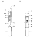
- FIG. 1 It is a figure which shows an example of the contact part of the negative voltage application terminal of the film-forming apparatus which concerns on other Embodiment 1.
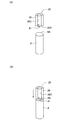
- FIG. 2 It is a figure which shows an example of the connection part of the film-forming apparatus which concerns on other Embodiment 2.
- FIG. 2 It is a figure which shows an example of the attachment state of the surface wave control member of the film-forming apparatus which concerns on other Embodiment 3.
- FIG. It is a figure which shows an example of the contact part of the negative voltage application terminal of the film-forming apparatus which concerns on other Embodiment 4.
- FIG. 5 It is a figure which shows an example of the contact part of the negative voltage application terminal of the film-forming apparatus which concerns on other Embodiment 5.
- a film forming apparatus 1 includes a processing container 2, a vacuum pump 3, a gas supply unit 5, a control unit 6, and the like.
- the processing container 2 is made of metal such as stainless steel and has a hermetic structure.
- the vacuum pump 3 is a pump capable of evacuating the inside of the processing container 2 via the pressure adjustment valve 7.
- a conductive material 8 to be deposited is held by a conductive holder 9 made of stainless steel or the like.
- the material of the work material 8 is not particularly limited as long as it has conductivity, but in the present embodiment, it is low-temperature tempered steel.
- the low temperature tempered steel is a material such as JIS G4051 (carbon steel for machine structural use), G4401 (carbon tool steel), G44-4 (alloy tool steel), or maraging steel.
- the workpiece material may be a ceramic or a resin coated with a conductive material.
- the gas supply unit 5 supplies a film forming source gas and an inert gas into the processing container 2. Specifically, an inert gas such as He, Ne, Ar, Kr, or Xe and a source gas such as CH 4 , C 2 H 2 , or TMS (tetramethylsilane) are supplied.
- an inert gas such as He, Ne, Ar, Kr, or Xe
- a source gas such as CH 4 , C 2 H 2 , or TMS (tetramethylsilane) are supplied.
- description will be made on the assumption that the material to be processed 8 is subjected to the DLC film formation process using CH 4 and TMS source gas.
- the flow rate and pressure of the raw material gas and the inert gas supplied from the gas supply unit 5 may be controlled via the control unit 6 or may be controlled by an operator.
- the source gas may be a gas containing a compound having a CH bond such as alkyne, alkene, alkane, aromatic compound, or a compound containing carbon.
- H 2 may be contained in the raw material gas.
- the plasma for performing the DLC film forming process on the material 8 to be processed held inside the processing container 2 is generated.
- This plasma is generated by the microwave pulse controller 11, the microwave oscillator 12, the microwave power source 13, the negative voltage power source 15, and the negative voltage pulse generator 16.
- surface wave excitation plasma is generated by a method disclosed in Japanese Patent Application Laid-Open No. 2004-47207 (hereinafter referred to as “MVP method (Microwave Voltage coupled Plasma method)”).
- MVP method Microwave Voltage coupled Plasma method
- the microwave pulse control unit 11 oscillates a pulse signal in accordance with an instruction from the control unit 6, and supplies the oscillated pulse signal to the microwave oscillator 12.
- the microwave oscillator 12 generates a microwave pulse according to the pulse signal from the microwave pulse controller 11.
- the microwave power source 13 supplies power to the microwave oscillator 12 that oscillates the microwave of 2.45 GHz with the instructed output in accordance with the instruction of the control unit 6. That is, the microwave oscillator 12 supplies a 2.45 GHz microwave to the isolator 17 described later as a pulsed microwave pulse according to the pulse signal from the microwave pulse control unit 11.
- the pulsed microwave pulse is projected from the microwave oscillator 12 through the isolator 17, the reflected energy detector 18A, the tuner 18, the waveguide 19, and the waveguide 19 through a coaxial waveguide converter (not shown). It is supplied to the processing surface of the holder 9 and the workpiece 8 through the coaxial waveguide 21 and the microwave supply port 22 made of a dielectric such as quartz that transmits microwaves.
- the isolator 17 prevents the reflected wave of the microwave from returning to the microwave oscillator 12.
- the tuner 18 matches the impedance before and after the tuner 18 so that the reflected wave of the microwave is minimized based on the phase and magnitude of the microwave reflected in the waveguide 19 detected by the reflected energy detector 18A. To do.
- the outer peripheral surface of the microwave supply port 22 excluding the upper end surface 22A is covered with a side electrode 23 formed of a metal such as stainless steel.
- the side electrode 23 is fixed to the inner side surface of the processing container 2 by screws or the like, and is electrically connected to the processing container 2.
- a central conductor of the coaxial waveguide 21 is extended at the center of the microwave supply port 22.
- the holder 9 is also on the extension of the central conductor and becomes the central conductor in the microwave supply port 22. Therefore, the central conductor of the microwave supply port 22 and the side electrode 23 function as a coaxial waveguide.
- the central conductor of the microwave supply port 22 is divided in the middle to maintain a vacuum, but may be penetrated if the vacuum is maintained by brazing with a dielectric or the like.
- the workpiece material 8 has, for example, a rod shape, and is held on an extension line of the central conductor of the microwave supply port 22. Instead of the holder 9, a part of the work material 8 may be held so as to be a central conductor in the microwave supply port 22.
- the work material 8 is disposed so as to protrude from the holder 9 holding the work material 8 toward the inside of the processing container 2 with respect to the microwave supply port 22.
- a negative voltage application terminal 25 for applying a negative bias voltage pulse is coaxially provided at the tip of the workpiece material 8 so as to protrude toward the inside of the processing container 2 with respect to the workpiece material 8. And electrically connected to the tip of the work material 8.
- the negative voltage application terminal 25 is formed in a cylindrical shape having an outer diameter substantially equal to the outer diameter of the workpiece 8.
- a plurality of contact portions 26 that contact the upper end surface 8 ⁇ / b> A of the workpiece material 8 are provided on the lower end surface 25 ⁇ / b> A on the workpiece material 8 side so as to protrude by a predetermined height. It is desirable to provide the contact portion 26 on the inner side from the outer peripheral surface side of the member on which the contact portion 26 is provided.
- a male screw portion 27 is formed up to the upper end portion inside the processing container 2 on the outer peripheral surface except from the lower end surface 25 ⁇ / b> A from which the contact portion 26 protrudes to a position at a predetermined height in the axial direction. ing.
- a portion from the lower end surface 25A of the negative voltage application terminal 25 to the male screw portion 27 is formed in a columnar shape having a predetermined height, and the outer peripheral portion of the upper end surface 8A of the workpiece 8 and the outer peripheral portion of the male screw portion 27 are in contact with each other.
- a connecting portion 28 that is continuously connected so as not to form a step across the portion 26 is formed.
- a negative voltage electrode 29 for applying a negative bias voltage pulse is electrically connected to the tip of the negative voltage application terminal 25 opposite to the workpiece 8 in the axial direction.
- One contact portion 26 may be provided so as to protrude from the lower end surface 25 ⁇ / b> A in the axial direction of the negative voltage application terminal 25.
- the substantially disc-shaped surface wave control member 32 is moved in the axial direction of the negative voltage application terminal 25 by fitting the female screw part 31 formed in the center part with the male screw part 27 of the negative voltage application terminal 25. It is provided as possible.
- a gear portion 33 On the outer peripheral surface of the surface wave control member 32, there is provided a gear portion 33 in which a plurality of linear teeth parallel to the rotation axis are formed over the entire circumference.
- the surface wave control member 32 is formed of stainless steel in the present embodiment, but may be formed of a metal such as aluminum or steel, or a dielectric such as ceramic or quartz. That is, as described later, the surface wave control member 32 has a reflectivity that reflects the microwave supplied from the microwave supply port 22 and propagating in the sheath layer in the direction opposite to the microwave supply direction. If it is,
- the drive shaft 35 is disposed in parallel with the axial direction of the negative voltage application terminal 25 in the processing container 2 and is rotatably supported.
- the drive shaft 35 is a drive in which a plurality of linear teeth that are substantially the same as the axial length of the male screw portion 27 and parallel to the rotation shaft are formed over the entire circumference at a portion facing the negative voltage application terminal 25.
- a gear portion 35A is provided.
- the drive gear portion 35 ⁇ / b> A is fitted to a gear portion 33 provided on the outer peripheral portion of the surface wave control member 32.
- the drive shaft 35 is connected at one end to a rotational drive force source 36 composed of a stepping motor or the like disposed on the outside of the processing container 2.
- the rotational driving force source 36 rotates the drive shaft 35 in accordance with an instruction from the control unit 6, thereby rotating the surface wave control member 32 via the gear unit 33 fitted to the drive gear unit 35 ⁇ / b> A. 32 is moved in the axial direction of the negative voltage application terminal 25 at a predetermined speed.
- a lead screw screw may be formed on the outer peripheral portion of the drive shaft 35, and a male screw portion fitted to the lead screw screw of the drive shaft 35 may be formed on the outer peripheral portion of the surface wave control member 32.
- the negative voltage application terminal 25 is almost entirely excluding the contact portions 26, and is made of a dielectric material such as ceramic, or a material containing at least one of molybdenum, tungsten, and silicon, or molybdenum, tungsten, and silicon. And a material containing at least one of the compounds.
- the negative voltage application terminal 25 is formed so as to be electrically connected from the portion where the negative voltage electrode 29 is electrically connected to the contact portion 26.
- the negative voltage application terminal 25 is a dielectric material such as ceramic at least at the portion on the workpiece 8 side of the surface wave control member 32 that may be exposed to the surface wave excitation plasma 45 except for the contact portions 26. Or a region covered with a material containing at least one of molybdenum, tungsten, and silicon, or a material containing a compound containing at least one of molybdenum, tungsten, and silicon. Good.
- the negative voltage power supply 15 supplies a negative bias voltage to the negative voltage pulse generator 16 in accordance with an instruction from the controller 6.
- the negative voltage pulse generator 16 pulses the negative bias voltage supplied from the negative voltage power supply 15. This pulsing process is a process in which the negative voltage pulse generator 16 controls the magnitude, cycle, duty ratio, etc. of the negative bias voltage pulse in accordance with an instruction from the controller 6.
- a negative bias voltage pulse which is a pulsed negative bias voltage, is applied to the workpiece 8 held inside the processing container 2 via the negative voltage electrode 29 and the negative voltage application terminal 25.
- a negative bias voltage pulse is applied to at least the entire surface of the work material 8. Is applied. Further, a negative bias voltage pulse is also applied to the entire surface of the negative voltage application terminal 25 and the holder 9 through the material to be processed 8.
- the surface wave excitation plasma 45 is generated by controlling the generated microwave pulse and the negative bias voltage pulse to be applied at the same time.
- the microwave is not limited to 2.45 GHz but may be any frequency from 0.3 GHz to 50 GHz.
- the negative voltage power supply 15 and the negative voltage pulse generator 16 are examples of the negative voltage application unit of the present invention.
- the microwave pulse control unit 11, the microwave oscillator 12, the microwave power source 13, the isolator 17, the reflected energy detection unit 18A, the tuner 18, the waveguide 19, and the coaxial waveguide 21 are examples of the microwave supply unit of the present invention. It is.
- the film forming apparatus 1 includes the negative voltage power supply 15 and the negative voltage pulse generation unit 16, but may include a positive voltage power supply and a positive voltage pulse generation unit.
- the control unit 6 includes a CPU, a RAM, a ROM, a hard disk drive (hereinafter referred to as “HDD”), a timer, and the like (not shown), and is configured from a computer.
- the control unit 6 outputs control signals to the negative voltage power supply 15 and the microwave power supply 13 to control the applied power of the microwave pulse and the applied voltage of the negative voltage pulse.
- the control unit 6 outputs a control signal to the negative voltage pulse generation unit 16 and the microwave pulse control unit 11 to generate the pulsed negative bias voltage pulse application timing, the supply voltage, and the microwave oscillator 12. Controls the supply timing and supply power of the microwave pulse.
- the control unit 6 outputs a flow rate control signal to the gas supply unit 5 to control the supply of the raw material gas and the inert gas.
- the control unit 6 outputs a control signal to the pressure adjustment valve 7 based on a pressure signal representing the pressure in the processing container 2 input from the vacuum gauge 37 attached to the processing container 2, and Control the pressure.
- the control unit 6 outputs a rotation control signal to the rotation driving force source 36, and controls a rotation amount for rotating the drive shaft 35 during the supply of the microwave. That is, the controller 6 controls the amount of movement by which the surface wave control member 32 is moved in the axial direction during the supply of microwaves.
- an essentially unipolar charged particle layer a so-called sheath layer
- the sheath layer is a layer having a low electron density, that is, positive polarity, and substantially has a relative dielectric constant in the microwave frequency band. It is a layer of ⁇ 1.
- the sheath thickness of the sheath layer can be increased by making the absolute value of the negative bias voltage to be applied larger than the absolute value of, for example, ⁇ 100V. That is, the sheath layer expands.
- This sheath layer acts as a dielectric that propagates surface waves to the interface between the plasma and the object in contact with the plasma.
- the microwave is supplied from the microwave supply port 22 disposed in the vicinity of one end of the holder 9 that holds the workpiece 8, and the negative voltage electrode 29 and the negative voltage 29 are supplied to the workpiece 8 and the holder 9.
- a negative bias voltage is applied via the voltage application terminal 25, the microwave propagates as a surface wave along the interface between the sheath layer and the plasma.
- high-density excitation plasma based on surface waves is generated along the surfaces of the negative voltage application terminal 25, the workpiece 8 and the holder 9.
- This high-density excitation plasma is the surface wave excitation plasma 45 described above.
- the electron density of the high-density plasma due to surface wave excitation in the vicinity of the surface of the workpiece 8 reaches 10 11 to 10 12 cm ⁇ 3 .
- the film formation speed is 3 to 30 times higher by one to two orders of magnitude than when the DLC film formation process is performed by plasma CVD with a normal negative bias voltage energy. (Nano m / sec) (10 ⁇ m in 1 hour) is obtained.
- the plasma CVD film formation time by the MVP method is 1/10 to 1/100 of the normal plasma CVD film formation time.
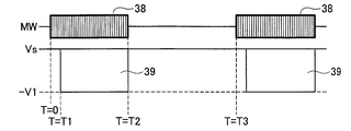
- the period of the microwave pulse 38 is T3 (seconds).
- the supply time for each pulse of the microwave pulse 38 is T2 (seconds), and in this embodiment, T2 is set to about 1 ⁇ 2 of T3.
- the application time of the negative bias voltage pulse 39 is (T2-T1) (seconds), and is set to 90% or more of the supply time T2 (seconds) of the microwave pulse 38.
- the application timing of the negative bias voltage pulse 39 is set to be delayed by T1 (seconds) from the supply start timing of the microwave pulse 38. That is, the negative bias voltage pulse 39 is applied after the microwave pulse 38 rises and the power is stabilized.
- the delay time T1 8 (microseconds).
- Information indicating the times T1, T2, and T3 (seconds) is stored in the ROM or HDD of the control unit 6.
- the negative bias voltage was 0V, ⁇ 200V, ⁇ 400V, and the plasma potential was + 30V. Therefore, the plasma electron density and the sheath thickness of the sheath layer were analyzed for sheath potentials of about ⁇ 30 V, about ⁇ 230 V, and about ⁇ 430 V, which are potentials of the workpiece 8 with respect to the plasma potential.
- the sheath thickness of the sheath layer when the negative bias voltage is 0 V is about 0.1 mm
- the negative bias The sheath thickness of the sheath layer when the voltage is ⁇ 200 V is about 0.5 mm
- the sheath thickness of the sheath layer when the negative bias voltage is ⁇ 400 V is about 0.9 mm.
- the sheath thickness of the sheath layer when the negative bias voltage is 0 V is about 0.06 mm, and the sheath layer when the negative bias voltage is ⁇ 200 V
- the sheath thickness of the sheath layer is about 0.4 mm, and when the negative bias voltage is ⁇ 400 V, the sheath thickness of the sheath layer is about 0.6 mm.
- the sheath thickness of the sheath layer increases as the negative bias voltage increases. That is, when the output power of the microwave pulse is made substantially constant and the electron density of the plasma is made almost constant, the sheath thickness of the sheath layer is made almost constant by setting the negative bias voltage constant at a predetermined voltage. The thickness can be maintained.
- the work material 8 is formed in a columnar shape having a diameter of 10 mm.
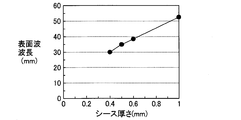
- the wavelength of the surface wave when the sheath thickness is about 0.4 mm is about 30 mm.
- the wavelength of the surface wave when the sheath thickness is about 0.6 mm is about 39 mm.
- the wavelength of the surface wave when the sheath thickness is about 1.0 mm is about 52 mm. Therefore, the wavelength of the surface wave becomes longer as the sheath thickness of the sheath layer increases. That is, by keeping the sheath thickness of the sheath layer substantially constant at a predetermined thickness, the wavelength of the surface wave is maintained substantially constant at a predetermined wavelength corresponding to the thickness of the sheath layer.
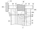
- the negative voltage application terminal 25 is continuously formed so as not to form a step between the outer peripheral portion of the upper end surface 8 ⁇ / b> A of the workpiece 8 and the contact portion 26 via the connecting portion 28. Since they are connected, the sheath layer 42 is continuously formed along the negative voltage application terminal 25 and the surface of the work material 8. Further, the female screw portion 31 of the surface wave control member 32 is fitted to the male screw portion 27 of the negative voltage application terminal 25 and is provided so as to be movable in the axial direction. In FIG. 5, the contour of the surface wave excitation plasma 45 is actually wavy as shown in FIG. 6 due to the influence of standing waves.
- the surface wave control member 32 has a substantially disk shape with a radius larger than at least the sheath thickness L2 of the sheath layer 42, and preferably extends to the outside of the plasma region of the surface wave excitation plasma 45 generated by microwaves. It is formed in a substantially disk shape with a radius. Further, it is formed between the height L1 of the contact portion 26, that is, the lower end surface 25A provided with the contact portion 26 of the negative voltage application terminal 25 and the upper end surface 8A with which the contact portion 26 of the workpiece 8 contacts. The gap height L1 is formed to be smaller than the sheath thickness L2 of the sheath layer 42. For this reason, the lower end surface 25A of the negative voltage application terminal 25, the contact portion 26, and the upper end surface 8A of the work material 8 are not exposed to plasma.
- the microwave propagating as a surface wave in the sheath layer 42 is reflected on the lower surface 32A of the surface wave control member 32 in a direction opposite to the microwave supply direction, that is, toward the upper end surface 22A side of the microwave supply port 22. Is done.
- the reflected surface wave is combined with the surface wave by the microwave supplied from the upper end surface 22A of the microwave supply port 22, and the surface wave is generated from the lower surface 32A of the surface wave control member 32 and the lower surface 32A of the surface wave control member 32.
- a standing wave having a node for each half wavelength is generated.
- the surface wave propagation length around the workpiece 8 is microwaves.
- the control unit 6 first drives the drive shaft 35 via the rotational drive force source 36 to obtain the surface wave control member 32 from the tip of the workpiece 8 in advance. And moved to a position that is a quarter wavelength away from the surface wave wavelength. Note that information on a position that is a quarter wavelength of the surface wave wavelength determined in advance from the tip of the workpiece 8 is stored in the ROM or HDD of the control unit 6.
- the surface wave reflected by the surface wave control member 32 generates a standing wave 43 having a local maximum at almost the tip of the material 8 to be processed.
- the plasma density of the surface wave excitation plasma 45 becomes the density distribution of the standing wave 43 having a node for every half wavelength of the surface wave wavelength. For this reason, in the plasma density distribution of the surface wave excitation plasma 45, a maximum portion where the plasma density is maximized is generated at the tip portion of the work material 8 and a plurality of locations in the longitudinal direction, and the plasma density is low between each maximum portion. Will occur.
- the control unit 6 rotates the drive shaft 35 via the rotational drive force source 36 to move the surface wave control member 32 from the tip of the workpiece 8 to the surface. It is moved to a position on the negative voltage electrode 29 side that is 1/2 wavelength away from the wave wavelength. That is, the surface wave control member 32 is moved to a position on the negative voltage electrode 29 side that is a quarter wavelength of the surface wave wavelength from the position shown in FIG. At this time, the surface wave reflected by the surface wave control member 32 generates a standing wave 46 having a node at almost the tip of the workpiece 8.
- the plasma density of the surface wave excitation plasma 45 becomes a density distribution of the standing wave 46 having a node for every half wavelength of the surface wave wavelength.
- the plasma density distribution of the surface wave excitation plasma 45 has a maximum portion where a node having a low plasma density is generated at a plurality of locations in the front end portion and the longitudinal direction of the work material 8, and the plasma density is maximized between the nodes. Will occur.
- the tuner 18 matches the impedance of the microwave in conjunction with the movement of the surface wave control member 32.
- the control unit 6 rotationally drives the drive shaft 35 via the rotational driving force source 36 so that the surface wave control member 32 has a surface wave wavelength in the axial direction of the negative voltage application terminal 25. Control is performed so that a position separated by a quarter wavelength, that is, a movement distance of a quarter wavelength of the surface wave wavelength is moved every predetermined time.
- the controller 6 rotationally drives the drive shaft 35 via the rotational driving force source 36 and positions the surface wave control member 32 at a distance of 1 ⁇ 4 wavelength of the surface wave wavelength in the axial direction of the negative voltage application terminal 25. Are controlled so as to move at a substantially constant speed during the supply of microwaves.
- the plasma density distribution of the surface wave excitation plasma 45 changes between the standing wave 43 and the standing wave 46 during film formation.
- the film characteristics such as the film thickness and film hardness of the DLC film formed on the film can be made uniform.
- the control unit 6 rotates the drive shaft 35 via the rotational driving force source 36 and separates the surface wave control member 32 in the axial direction of the negative voltage application terminal 25 by 1 ⁇ 4 wavelength or more of the surface wave wavelength.
- the position for example, a position separated by an integral multiple of 1 ⁇ 2 wavelength may be controlled to move at a substantially constant speed during the microwave supply.
- the film characteristics such as the film thickness and film hardness of the DLC film formed on the surface can be made more uniform.
- the movement of the surface wave control member 32 during the supply of microwaves may be unidirectional or reciprocal. However, in the case of reciprocal movement, it is desirable to reduce the acceleration time, the deceleration time, the stop time, and the number of reciprocations. Alternatively, the supply of microwaves may be stopped while the moving speed of the surface wave control member 32 varies.
- the surface wave control member 32 provided so as to protrude from the outer peripheral portion of the negative voltage application terminal 25 to the outside in the sheath thickness direction of the sheath layer 42 includes the sheath
- the microwave propagating as a high energy density surface wave in the layer 42 is reflected.
- the surface wave is reflected by the surface wave control member 32 in the direction opposite to the microwave supply direction, so that the surface wave control member 32 provided at the negative voltage application terminal 25 moves to the negative voltage electrode 29 side.
- the progress of the surface wave to the unintended part can be reliably suppressed. Therefore, it is possible to reliably suppress the propagation of the surface wave to the wiring or the like connected to the negative voltage application terminal 25 via the negative voltage electrode 29, and to reduce wasteful consumption of energy.
- the surface wave is reflected by the surface wave control member 32 in the direction opposite to the microwave supply direction, that is, toward the upper end surface 22A of the microwave supply port 22, and plasma is also generated by the reflected wave. For this reason, the plasma density of the surface wave excitation plasma 45 becomes high. As a result, it is possible to shorten the film formation time for forming the DLC film on the processing surface of the material 8 to be processed, thereby reducing wasteful consumption of energy.
- control unit 6 rotationally drives the drive shaft 35 via the rotational driving force source 36 to move the surface wave control member 32 in the propagation direction in which the microwave propagates in the sheath layer 42, so that a desired position is obtained.
- the reflection position where the microwave is reflected can be changed.
- the distribution of the standing wave generated by the microwave propagating in the sheath layer 42 as a surface wave with a high energy density can be changed to change the distribution of the plasma density.
- a DLC film can be formed.
- the operator confirms the state of the surface wave excited plasma 45 generated around the workpiece 8 from the quartz window 48 (see FIG. 1) provided on the side wall of the processing vessel 2. Then, an operator inputs an instruction signal for instructing the controller 6 to rotate the drive shaft 35 and move the surface wave control member 32 by a predetermined distance via an operation unit (not shown). It may be configured. Thereby, the distribution of the standing wave generated by the microwave propagating in the sheath layer 42 as a surface wave with a high energy density can be changed to change the distribution of the plasma density.
- a DLC film can be formed.
- control unit 6 rotationally drives the drive shaft 35 via the rotational driving force source 36 to move the surface wave control member 32 at least 1/4 wavelength of the surface wave wavelength in the axial direction of the negative voltage application terminal 25.
- the position is controlled to move at a constant speed every predetermined time.
- the control unit 6 can change the reflection position where the microwave is reflected at a constant speed during the supply of the microwave, and the microwave propagates in the sheath layer 42 as a surface wave with a high energy density.
- the distribution of the generated standing wave can be made uniform. Therefore, the plasma density distribution of the high-density plasma of the source gas plasma-excited by the surface wave can be made uniform, and variation in the film thickness distribution of the DLC film formed on the surface of the workpiece 8 can be suppressed. Can do.
- the tuner 18 matches the impedance of the microwave in conjunction with the movement of the surface wave control member 32. Thereby, the reflection of the microwave can be reduced, the microwave can be efficiently supplied, and the variation in the film thickness distribution of the DLC film formed on the surface of the material 8 to be processed can be suppressed with a simple configuration. .
- At least a portion of the negative voltage application terminal 25 closer to the workpiece 8 than the surface wave control member 32 is a dielectric, a dielectric, or a material containing at least one of molybdenum, tungsten, and silicon, or , And a material containing at least one compound of molybdenum, tungsten, and silicon.
- the space between the lower end surface 25A provided with the contact portion 26 of the negative voltage application terminal 25 and the upper end surface 8A with which the contact portion 26 of the workpiece 8 contacts is larger than the sheath thickness L2 of the sheath layer 42.
- a gap having a small height L1 is formed.
- the negative voltage application terminal 25 is a connecting portion 28 that continuously connects the outer peripheral portion of the upper end surface 8A of the work material 8 and the outer peripheral portion of the male screw portion 27 with no contact portion interposed therebetween. have.
- reflection by the discontinuous part of the microwave propagating as a surface wave in the sheath layer 42 can be eliminated, and the surface wave can be reflected by the surface wave control member 32. Therefore, even if the surface wave control member 32 is moved in the axial direction of the male screw portion 27, the surface wave can be reflected by the surface wave control member 32, and the film thickness of the DLC film formed on the surface of the work material 8. Distribution variation can be suppressed.
- FIG. 7 a film forming apparatus 51 according to another first embodiment will be described with reference to FIG.
- the schematic configuration of the film forming apparatus 51 according to the other first embodiment is substantially the same as the configuration of the film forming apparatus 1 shown in FIGS.
- a thin plate contact portion 52 formed of stainless steel for springs is provided instead of the cylindrical contact portion 26 protruding from the lower end surface 25A of the negative voltage application terminal 25, a thin plate contact portion 52 formed of stainless steel for springs is provided. It is different in point.
- one end of the thin plate contact portion 52 is attached to the lower end surface 25A of the negative voltage application terminal 25 so that it can be bent. Further, the contact portion 52 is formed to have a thickness smaller than the sheath thickness L2 of the sheath layer 42. Therefore, as shown in FIG. 7B, when the negative voltage application terminal 25 is placed on the upper end surface 8A of the workpiece material 8 and electrically connected to the upper end surface 8A of the workpiece material 8. The contact portion 52 is elastically bent toward the lower end face 25A side of the negative voltage application terminal 25 around the one end portion, and is arranged in a state of being sandwiched between the negative voltage application terminal 25 and the workpiece 8.
- a gap having a height smaller than the sheath thickness L ⁇ b> 2 of the sheath layer 42 is formed between the lower end surface 25 ⁇ / b> A of the negative voltage application terminal 25 and the upper end surface 8 ⁇ / b> A of the workpiece 8.
- the contact portion 52 of the negative voltage application terminal 25 elastically presses the upper end surface 8A of the workpiece material 8, the contact portion 52 is reliably brought into contact with the upper end surface 8A of the workpiece material 8, thereby Can be connected. Further, the lower end surface 25A of the negative voltage application terminal 25, the contact portion 52, and the upper end surface 8A of the workpiece material 8 can be prevented from being exposed to plasma, and the contact portion 52 of the negative voltage application terminal 25 and the workpiece material 8 can be prevented from being exposed to plasma. Conduction failure can be suppressed.
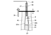
- FIG. 8 a film forming apparatus 55 according to another second embodiment will be described with reference to FIG.
- the schematic configuration of the film forming apparatus 55 according to the other second embodiment is substantially the same as the structure of the film forming apparatus 1 shown in FIGS.
- a negative voltage application terminal 56 is provided instead of the negative voltage application terminal 25.
- the outer diameter of the work material 57 is larger than the outer diameter of the work material 8 attached to the film forming apparatus 1 shown in FIGS.
- the contour of the surface wave excitation plasma 45 is actually wavy due to the influence of standing waves.
- a cylindrical contact portion 58 that contacts the upper end surface 57 ⁇ / b> A of the material 57 to be processed is approximately at the center of the lower end surface 56 ⁇ / b> A of the negative voltage application terminal 56, rather than the sheath thickness of the sheath layer 61. It protrudes at a small height.
- the outer diameter of the work material 57 is larger than the outer diameter of the male screw portion 27 of the negative voltage application terminal 56.
- the portion from the lower end surface 56A from which the contact portion 58 of the negative voltage application terminal 56 projects to the male screw portion 27 is formed in a truncated cone, and the outer peripheral portion of the upper end surface 57A of the work material 57 and the outer periphery of the male screw portion 27.
- the connection part 59 which connects a part continuously without a level
- the connecting portion 59 has a lower end having an outer diameter substantially equal to the outer diameter of the work material 57, an upper end having an outer diameter substantially equal to the outer diameter of the male screw portion 27, and an outer peripheral surface having a small inclination angle ⁇ , for example, an inclination. It is formed in a truncated cone inclined at an angle ⁇ of 5 degrees to 10 degrees. That is, the connecting portion 59 is formed in a cross-sectional shape having a size between the cross-sectional shape of the male screw portion 27 of the negative voltage application terminal 56 and the cross-sectional shape of the workpiece material 57.
- the negative voltage application terminal 56 of the film forming apparatus 55 is stepped from the upper end surface 57 ⁇ / b> A on the workpiece material 57 side to the lower end portion of the male screw portion 27 with respect to the tip portion of the workpiece material 57. It has the connection part 59 connected continuously. Thereby, even if the outer diameter of the material 57 to be processed is different from the outer diameter of the male screw portion 27, the reflection by the discontinuous portion of the microwave propagating in the sheath layer 61 as the surface wave is eliminated, and the surface wave is converted into the surface wave. The light can be reflected by the control member 32.
- FIG. 9 a film forming apparatus 65 according to another third embodiment will be described with reference to FIG.
- the schematic configuration of the film forming apparatus 65 according to the other third embodiment is substantially the same as the structure of the film forming apparatus 1 shown in FIGS.
- a surface wave control member 66 and an inclusion 67 interposed between the surface wave control member 66 and the negative voltage application terminal 25 are provided.
- the surface wave control member 66 is made of a metal such as aluminum, stainless steel, or steel.
- the inclusion 67 is made of a dielectric material such as ceramic or quartz.
- the contour of the surface wave excited plasma 45 is actually wavy due to the influence of standing waves.
- the inclusion 67 is formed radially outward from the outer peripheral surface of the main body portion 67A formed in a substantially cylindrical shape and the end edge portion of the main body portion 67A on the workpiece 8 side. It is comprised from the flange part 67B extended and formed in the front view ring shape. Further, the height from the upper end of the outer peripheral portion of the main body 67 ⁇ / b> A to the flange 67 ⁇ / b> B is formed to be approximately the same as the thickness of the surface wave control member 66. On the inner peripheral surface of the inclusion 67, a female screw portion 68 that is fitted to the male screw portion 27 of the negative voltage application terminal 25 is formed.
- the flange portion 67 ⁇ / b> B of the inclusion 67 is formed to have a radius larger than at least the sheath thickness of the sheath layer 42 so that the outer peripheral surface protrudes radially outward from the sheath layer 42.
- the flange portion 67B is formed to have a radius that the outer peripheral surface extends to the outside of the plasma region of the surface wave excited plasma 45 generated by microwaves.
- the surface wave control member 66 has a through hole 66A having an inner diameter substantially equal to the outer diameter of the main body portion 67A of the inclusion 67 at the center, and a substantially ring having an outer diameter larger than the flange portion 67B of the inclusion 67. It is formed in a shape.
- the surface wave control member 66 is formed to have a plate thickness substantially equal to the length of the main body portion 67A of the inclusion 67, and a gear portion 33 fitted to the drive gear portion 35A of the drive shaft 35 is formed on the outer peripheral surface thereof. Yes.
- the surface wave control member 66 is inserted into the through hole 66A with the main body portion 67A of the inclusion 67 from the workpiece material 8 side, and the end surface 66B on the workpiece material 8 side is in contact with the flange portion 67B. It is connected to the inclusion 67 so as not to rotate relative to the inclusion 67 by an adhesive or the like.
- a spline is formed on the outer peripheral surface of the main body portion 67A of the inclusion 67
- a spline groove is formed on the inner peripheral surface of the through hole 66A of the surface wave control member 66, and the main body portion 67A is press-fitted into the through hole 66A. Accordingly, the surface wave control member 66 may be connected to the inclusion 67 so as not to be relatively rotatable.
- the control unit 6 rotates and drives the drive shaft 35 via the rotational driving force source 36 to rotate the surface wave control member 66 and the inclusion 67, thereby causing the surface wave control member 66 and the inclusion 67 to be negative voltage.
- the application terminal 25 can be moved up and down in the axial direction. Further, by providing an inclusion 67 formed of a dielectric between the surface wave control member 66 and the negative voltage application terminal 25, the surface wave propagating in the sheath layer 42 by the inclusion 67 is directed in the microwave supply direction. On the other hand, the light can be reflected in the opposite direction, that is, toward the upper end surface 22A of the microwave supply port 22.
- FIG. 10A The schematic configuration of the film forming apparatus 71 according to the other fourth embodiment is substantially the same as the structure of the film forming apparatus 1 shown in FIGS.
- the negative voltage application terminal 25 protrudes from the end face of the connecting portion 28 on the workpiece 8 side by a predetermined height in the axial direction with an outer diameter smaller than the outer diameter of the connecting portion 28.
- the protruding portion 28A is formed coaxially.
- a protective cylinder 72 having a substantially same outer diameter as the connecting portion 28 and longer than the protruding portion 28A surrounds the protruding portion 28A. It is attached coaxially.
- the protective cylinder 72 is formed of a dielectric material such as ceramic.
- a compression coil spring 73 having one end attached to the end surface of the protruding portion 28A on the workpiece 8 side, and a cylindrical contact portion 75 to which the other end of the compression coil spring 73 is attached, Are arranged on the same axis.
- the outer diameter of the contact portion 75 is formed to be substantially the same as the outer diameter of the protruding portion 28A. Further, the contact portion 75 is disposed so as to slightly protrude outward in the axial direction from the protective cylinder 72, and is provided so as to be able to be accommodated in the protective cylinder 72 by compressing the compression coil spring 73. Therefore, as shown in FIG. 10B, when the negative voltage application terminal 25 is placed on the tip of the work material 8, the lower end surface 72 ⁇ / b> A of the protective cylinder 72 is the upper end surface of the work material 8. 8A is abutted and arranged on the same axis. The contact portion 75 is housed in the protective cylinder 72 against the urging force of the compression coil spring 73 by the upper end surface 8A of the workpiece 8.
- the contact part 75 of the negative voltage application terminal 25 can be reliably brought into contact with the upper end surface 8A of the material 8 to be electrically connected. Further, when the negative voltage application terminal 25 is placed on the tip of the workpiece 8, the projecting portion 28 ⁇ / b> A, the compression coil spring 73, and the contact portion 75 are accommodated in a protective cylinder 72 formed of a dielectric. At the same time, the upper end surface 8 A of the work material 8 is covered with the lower end portion of the protective cylinder 72.
- the protrusion 28A, the compression coil spring 73 and the contact portion 75, and the upper end surface 8A of the work material 8 from being exposed to plasma, and the contact portion 75 of the negative voltage application terminal 25 and the work material 8 can be prevented. Conduction failure can be suppressed. Further, the surface wave that has propagated through the sheath layer on the surface of the material to be processed 8 continues to propagate as a surface wave at the interface between the surface of the protective cylinder 72 formed of a dielectric and the plasma. The reflection at the end face 8A can be suppressed.
- a film forming apparatus 78 according to another fifth embodiment will be described with reference to FIG.
- the schematic configuration of the film forming apparatus 78 according to the other fifth embodiment is substantially the same as the structure of the film forming apparatus 1 shown in FIGS.
- a shaft hole 28C having a predetermined inner diameter is formed coaxially with a predetermined depth on the inner side in the axial direction from the lower end surface 25A of the connecting portion 28 on the workpiece 8 side.
- a thin plate contact portion 81 made of stainless steel for springs is provided instead of the columnar contact portion 26. It is different in point.
- the thin plate-like contact portion 81 has one end attached to the inner peripheral surface of the workpiece material 8 side edge portion of the shaft hole 28C and the other end side in the axial direction from the shaft hole 28C. It is inclined so as to protrude diagonally outward.
- the length of the inclined portion of the contact portion 81 is formed to be smaller than the inner diameter of the shaft hole 28C. Therefore, as shown in FIG. 11B, when the negative voltage application terminal 25 is placed on the upper end surface 8A of the workpiece material 8, the lower end surface 25A of the connecting portion 28 is the upper end surface of the workpiece material 8. 8A is abutted and arranged on the same axis. Further, the contact portion 81 is elastically bent into the shaft hole 28C by the upper end surface 8A of the work material 8 and accommodated in the shaft hole 28C, and elastically presses the upper end surface 8A of the work material 8. To do.
- the contact portion 81 of the negative voltage application terminal 25 elastically presses the upper end surface 8A of the workpiece material 8, the contact portion 81 is reliably brought into contact with the application side end surface portion of the workpiece material 8, Can be electrically connected. Further, when the negative voltage application terminal 25 is placed on the upper end surface 8A of the work material 8, the contact portion 81 is accommodated in the shaft hole 28C, and the upper end surface 8A of the work material 8 is connected to the connecting portion 28. The lower end surface 25A is covered. For this reason, it can prevent that the contact part 81 and the upper end surface 8A of the workpiece material 8 are exposed to plasma, and the conduction failure between the contact part 81 of the negative voltage application terminal 25 and the workpiece material 8 can be suppressed.
- the surface wave control member 32 of the film forming apparatus 1 shown in FIGS. 1 to 6 may be formed of ferrite or the like so that the surface wave control member 32 has an absorptivity for absorbing microwaves.
- the surface wave control member 32 provided so as to protrude from the outer peripheral portion of the negative voltage application terminal 25 in the sheath thickness direction of the sheath layer 42 is a microwave that propagates in the sheath layer 42 as a surface wave of high energy density. To absorb.
- the surface wave is absorbed by the surface wave control member 32, the progress of the surface wave from the surface wave control member 32 provided at the negative voltage application terminal 25 to the negative voltage electrode 29 side can be suppressed. Therefore, the propagation of the surface wave to the wiring connected to the negative voltage electrode 29 of the negative voltage application terminal 25 is suppressed, and the member connected to the negative voltage electrode 29 side is prevented from being exposed to plasma. Can do.
- the sheath layer 42 is interrupted before the surface wave control member 32. For this reason, a part of the surface wave is reflected in the opposite direction to the microwave supply direction at the interrupted portion of the sheath layer 42, that is, the upper end surface 22A side of the microwave supply port 22, and the reflected wave also Plasma is generated. For this reason, the plasma density of the surface wave excitation plasma 45 becomes high. As a result, it is possible to shorten the film formation time for forming the DLC film on the processing surface of the material 8 to be processed, thereby reducing wasteful consumption of energy.
Landscapes
- Chemical & Material Sciences (AREA)
- Physics & Mathematics (AREA)
- Engineering & Computer Science (AREA)
- Plasma & Fusion (AREA)
- Metallurgy (AREA)
- Chemical Kinetics & Catalysis (AREA)
- Materials Engineering (AREA)
- Mechanical Engineering (AREA)
- General Chemical & Material Sciences (AREA)
- Organic Chemistry (AREA)
- Analytical Chemistry (AREA)
- Electromagnetism (AREA)
- Spectroscopy & Molecular Physics (AREA)
- Inorganic Chemistry (AREA)
- Plasma Technology (AREA)
- Chemical Vapour Deposition (AREA)
Abstract
導電性を有する被加工材料の処理表面に沿ってプラズマを生成させるためのマイクロ波を供給するマイクロ波供給部と、被加工材料の処理表面に沿うシース層を拡大させる負のバイアス電圧を被加工材料に印加する負電圧印加部と、マイクロ波供給部から供給されるマイクロ波を拡大されたシース層へ伝搬させるマイクロ波供給口と、マイクロ波供給口に対して被加工材料の少なくとも一部を挟む位置に設けられ、負電圧印加部によって印加される負のバイアス電圧を被加工材料に印加させる負電圧印加端子部材と、負電圧印加端子部材の外周部からシース層のシース厚さ方向に突出して設けられ、シース層内を伝搬するマイクロ波に対して反射能を有する表面波制御部材と、を備える。
Description
本発明は、プラズマを用い、鋼材等の導電性を有する被加工材料の表面に皮膜を形成するための成膜装置に関するものである。
従来より、プラズマを用い、鋼材等の導電性を有する被加工材料の表面に皮膜を形成するための成膜装置に関し種々提案されている。
例えば、上述した被加工材料の表面にダイヤモンドライクカーボン(以下、「DLC」という。)成膜処理する技術が特開2004-47207号公報等に開示されている。
例えば、上述した被加工材料の表面にダイヤモンドライクカーボン(以下、「DLC」という。)成膜処理する技術が特開2004-47207号公報等に開示されている。
この特開2004-47207号公報に開示された技術では、プラズマ生成装置がマイクロ波供給口である石英窓を通して処理容器内の被加工材料に向けマイクロ波を供給することにより、石英窓内面の周辺領域にプラズマが生成される。被加工材料は例えば棒状であり、石英窓内面から処理容器内に突出するように配置され、生成されたプラズマに覆われた被加工材料の石英窓内面の周辺部分にはシース層が生成される。続いて、マイクロ波の供給中に、プラズマ生成装置が被加工材料へ負のバイアス電圧を印加する。
この結果、被加工材料の表面に生成されたシース層は被加工材料の表面に沿って拡大する。また同時に、供給されたマイクロ波は、この拡大されたシース層に沿って高エネルギー密度の表面波として伝搬する。このとき、高エネルギー密度の表面波により石英窓内面周辺から離れた被加工材料の表面にもプラズマが生成され、シース層も生成される。この新たに生成されたシース層も負のバイアス電圧によって拡大され、この拡大されたシース層に沿ってマイクロ波が高エネルギー密度の表面波としてさらに伝搬する。これにより、被加工材料の石英窓周辺から離れた部分へ、すなわち、被加工材料の石英窓側の一端から処理容器内に突出した他端へとプラズマが伸長する。この結果、原料ガスが表面波によってプラズマ励起されて高密度プラズマとなり、被加工材料の表面全体にDLC成膜処理される。
しかしながら、特開2004-47207号公報に開示された技術では、被加工材料から負のバイアス電圧を印加する負電圧印加端子へ高エネルギー密度の表面波が伝搬し、更に、負電圧印加端子及び負電圧印加端子に接続されている配線等の意図しない部分にまで表面波が伝搬する可能性がある。この結果、エネルギーが無駄に消費される虞がある。
そこで、本発明は、上述した問題点を解決するためになされたものであり、負電圧印加端子部材に接続されている配線等への表面波の伝搬を抑制し、エネルギーの無駄な消費を抑えることができる成膜装置を提供することを目的とする。
前記目的を達成するため本発明の成膜装置は、導電性を有する被加工材料の処理表面に沿ってプラズマを生成させるためのマイクロ波を供給するマイクロ波供給部と、前記被加工材料の処理表面に沿うシース層を拡大させる負のバイアス電圧を前記被加工材料に印加する負電圧印加部と、前記マイクロ波供給部から供給されるマイクロ波を拡大された前記シース層へ伝搬させるマイクロ波供給口と、前記マイクロ波供給口に対して前記被加工材料の少なくとも一部を挟む位置に設けられ、前記負電圧印加部によって印加される負のバイアス電圧を前記被加工材料に印加させる負電圧印加端子部材と、前記負電圧印加端子部材の外周部から前記シース層のシース厚さ方向に突出して設けられ、前記シース層内を伝搬する前記マイクロ波に対して反射能又は吸収能を有する表面波制御部材と、を備えることを特徴とする。
このような成膜装置では、負電圧印加端子部材の外周部からシース層のシース厚さ方向に突出するように設けられた表面波制御部材は、シース層内を高エネルギー密度の表面波として伝搬するマイクロ波を反射又は吸収する。これにより、表面波は表面波制御部材によって反射又は吸収されるため、負電圧印加端子部材に設けられた表面波制御部材から負電圧印加部側へ、つまり、意図しない部分への表面波の進行を抑制することができる。従って、負電圧印加端子部材に接続されている配線等への表面波の伝搬を抑制し、エネルギーの無駄な消費を抑えることができる。
表面波制御部材がシース層内を伝搬するマイクロ波に対して反射能を有する場合は、表面波制御部材によって表面波がマイクロ波供給方向に対して反対方向へ反射され、その反射波によってもプラズマが生成されるため、プラズマ密度が高くなる。この結果、被加工材料の処理表面に皮膜を成膜する成膜時間を短縮して、エネルギーの無駄な消費を低減することができる。
表面波制御部材がシース層内を伝搬するマイクロ波に対して吸収能を有する場合は、表面波制御部材の手前でシース層が途切れる。このため、このシース層の途切れた箇所で表面波の一部がマイクロ波供給方向に対して反対方向へ反射され、その反射波によってもプラズマが生成され、プラズマ密度が高くなる。この結果、被加工材料の処理表面に皮膜を成膜する成膜時間を短縮して、エネルギーの無駄な消費を低減することができる。
また、前記本発明の成膜装置において、前記表面波制御部材は、前記シース層よりもシース厚さ方向外側へ突出するように設けられているようにしてもよい。
このような成膜装置では、表面波制御部材は、シース層よりもシース厚さ方向外側へ突出するように設けられている。これにより、負電圧印加端子部材に設けられた表面波制御部材から負電圧印加部側へのシース層内を伝搬する表面波の進行を確実に抑制することができる。従って、負電圧印加端子部材に接続されている配線等への表面波の伝搬を確実に抑制し、エネルギーの消費を低減することができる。
また、前記本発明の成膜装置において、前記表面波制御部材は、前記シース層内を伝搬する前記マイクロ波に対して反射能を有し、且つ、前記マイクロ波が前記シース層内を伝搬する伝搬方向に移動可能に設けられているようにしてもよい。
このような成膜装置では、表面波制御部材をマイクロ波がシース層内を伝搬する伝搬方向に移動させることによって、マイクロ波の表面波制御部材によって反射される反射位置が変化する。これにより、表面波制御部材から負電圧印加部側への表面波の進行を抑制し、エネルギーの無駄な消費を抑えることができる。更に、シース層内を高エネルギー密度の表面波として伝搬するマイクロ波によって生成される定在波の分布を変化させて、マイクロ波がシース層内を伝搬する伝搬方向に対する被加工材料の処理表面周囲のプラズマ密度の分布を変化させることができ、被加工材料に合わせて成膜することができる。
また、前記本発明の成膜装置において、前記表面波制御部材は、前記マイクロ波供給部によるマイクロ波の供給中に移動可能に設けられているようにしてもよい。
このような成膜装置では、マイクロ波供給部によるマイクロ波の供給中に、表面波制御部材をマイクロ波がシース層内を伝搬する伝搬方向に移動させることによって、マイクロ波の反射される反射位置が、マイクロ波の供給中に変化する。これにより、シース層内を高エネルギー密度の表面波として伝搬するマイクロ波によって生成される定在波の分布を成膜時間全体において均一化することができる。従って、表面波によってプラズマ励起された原料ガスの高密度プラズマのマイクロ波がシース層内を伝搬する伝搬方向に対する被加工材料の処理表面周囲のプラズマ密度の分布を成膜時間全体において均一化することができ、被加工材料の表面に形成された皮膜の膜厚分布のバラツキを抑制することができる。
また、前記本発明の成膜装置において、前記表面波制御部材は、前記シース層内を伝搬する前記マイクロ波によって生成される表面波の少なくとも1/4波長の距離を移動可能に設けられているようにしてもよい。
このような成膜装置では、マイクロ波の供給中に、表面波制御部材はマイクロ波によって生成される表面波の少なくとも1/4波長の距離を移動する。これにより、表面波によって生成される定在波の分布を表面波の少なくとも1/4波長の範囲内で変化させることが可能となる。従って、シース層内を高エネルギー密度の表面波として伝搬するマイクロ波によって生成される定在波の分布を成膜時間全体において更に均一化することができ、被加工材料の表面に形成された皮膜の膜厚分布のバラツキを更に抑制することができる。
また、前記本発明の成膜装置において、前記マイクロ波供給部にインピーダンスを整合するインピーダンス整合部を備え、前記インピーダンス整合部は、前記表面波制御部材の移動に連動して前記マイクロ波のインピーダンスを整合するようにしてもよい。
このような成膜装置では、インピーダンス整合部は、表面波制御部材の移動に連動してマイクロ波のインピーダンスを整合する。これにより、マイクロ波の出力を安定化させて効率よくマイクロ波を供給することができると共に、簡易な構成で被加工材料の表面に形成された皮膜の膜厚分布のバラツキを抑制することができる。
また、前記本発明の成膜装置において、前記負電圧印加端子部材は、前記被加工材料との接点部を除き、前記プラズマに晒される可能性がある少なくとも前記表面波制御部材よりも前記被加工材料側の部分において、誘電体、又は、モリブデンとタングステンとシリコンとの少なくともいずれか1つを含む材料、若しくは、モリブデンとタングステンとシリコンとのうちの少なくともいずれか1つの化合物を含む材料で被覆された領域を有するようにしてもよい。
このような成膜装置では、負電圧印加端子部材の少なくとも表面波制御部材よりも被加工材料側の部分は、誘電体、又は、モリブデンとタングステンとシリコンとの少なくともいずれか1つを含む材料、若しくは、モリブデンとタングステンとシリコンとのうちの少なくともいずれか1つの化合物を含む材料で被覆されている。これにより、負電圧印加端子部材の高密度プラズマによる劣化を抑止することができる。
また、前記本発明の成膜装置において、誘電体で形成されて、前記表面波制御部材と前記負電圧印加端子部材との間に介在する介在物を備えるようにしてもよい。
このような成膜装置では、表面波制御部材と負電圧印加端子部材との間に誘電体で形成された介在物が設けられている。これにより、介在物によってシース層内を伝搬する表面波をより反射することができる。また、表面波制御部材への負のバイアス電圧の印加を低減し、表面波制御部材周辺におけるシース層の拡大を低減できる。従って、負電圧印加端子部材に設けられた表面波制御部材から負電圧印加部側への表面波の進行を抑制し、エネルギーの消費を更に低減することができる。
また、前記本発明の成膜装置において、前記負電圧印加端子部材の前記被加工材料との接点部が設けられた接点側端面部と、前記被加工材料の前記接点部が接触する印加側端面部との間には、前記シース層のシース厚さよりも小さい距離の隙間が形成されているようにしてもよい。
このような成膜装置では、連結部を含む負電圧印加端子部材の接点部は、負電圧印加端子部材の接点側端面部から、被加工材料の周囲及び負電圧印加端子部材の周囲に形成されるシース層のシース厚さよりも小さい距離だけ突出して形成されている。これにより、負電圧印加端子部材の接点部を被加工材料の印加側端面部に確実に接触させることができ、負電圧印加端子部材の接点部と被加工材料との導通不良を抑止することができる。また、負電圧印加端子部材の接点側端面部と被加工材料の印加側端面部がプラズマに晒されることを防止でき、負電圧印加端子部材の接点部の劣化を抑止することができる。
また、前記本発明の成膜装置において、前記負電圧印加端子部材は、前記シース層内を前記マイクロ波が表面波として伝搬する伝搬方向において、前記被加工材料に対して連続部を形成する形状を有するようにしてもよい。
このような成膜装置では、負電圧印加端子部材は、被加工材料に対して連続部を形成する形状を有している。これにより、シース層内を表面波として伝搬するマイクロ波の不連続部による反射を無くして、表面波を表面波制御部材で反射又は吸収することができる。従って、被加工材料に合わせて皮膜を形成することができる。
更に、前記本発明の成膜装置において、前記負電圧印加端子部材は、前記被加工材料との間に、前記シース層のシース厚さ方向において、前記負電圧印加端子部材の断面形状と前記被加工材料の断面形状との間の大きさの断面形状に形成された連結部を有するようにしてもよい。
このような成膜装置では、負電圧印加端子部材の断面形状と被加工材料の断面形状との大きさが異なっても、連結部を介して負電圧印加端子部材と被加工材料との各端部を連続的に繋ぐことが可能となる。これにより、表面波として伝搬するマイクロ波の不連続部による反射を無くして、表面波を表面波制御部材で反射又は吸収することができる。従って、被加工材料に合わせて皮膜を形成することができる。
以下、本発明に係る成膜装置について具体化した一実施形態に基づき図面を参照しつつ詳細に説明する。先ず、本実施形態に係る成膜装置1の概略構成について図1及び図5に基づいて説明する。
図1に示すように、本実施形態に係る成膜装置1は、処理容器2、真空ポンプ3、ガス供給部5、及び制御部6等から構成されている。処理容器2は、ステンレス等の金属製であって、気密構造の処理容器である。真空ポンプ3は、圧力調整バルブ7を介して処理容器2の内部を真空排気可能なポンプである。処理容器2の内部には、成膜対象である導電性を有する被加工材料8が、ステンレス等で形成された導電性を有する保持具9により保持されている。
被加工材料8の材質は、導電性を有していれば、特に限定されるものではないが、本実施形態では低温焼戻し鋼である。ここで低温焼戻し鋼とは、JIS G4051(機械構造用炭素鋼鋼材)、G4401(炭素工具鋼鋼材)、G44-4(合金工具用鋼材)、又はマルエージング鋼材などの材料である。被加工材料は、低温焼戻し鋼以外にも、セラミック、または樹脂に導電性の材料がコーティングされているものでもよい。
ガス供給部5は、処理容器2の内部に成膜用の原料ガスと不活性ガスとを供給する。具体的には、He、Ne、Ar、Kr、またはXeなどの不活性ガスとCH4、C2H2、又はTMS(テトラメチルシラン)等の原料ガスとが供給される。本実施形態では、CH4、およびTMSの原料ガスにより被加工材料8がDLC成膜処理されるとして説明する。
また、ガス供給部5から供給される原料ガス、および不活性ガスの流量、および圧力が制御部6を介して制御されてもよいし、作業者により制御されてもよい。また、原料ガスは、アルキン、アルケン、アルカン、芳香族化合物などのCH結合を有する化合物、または炭素が含まれる化合物が含まれるガスであればよい。また、H2が原料ガスに含まれてもよい。
処理容器2の内部に保持された被加工材料8に対してDLC成膜処理を行うためのプラズマが発生される。このプラズマは、マイクロ波パルス制御部11、マイクロ波発振器12、マイクロ波電源13、負電圧電源15、及び負電圧パルス発生部16により発生される。本実施形態では、特開2004-47207号公報に開示された方法(以下、「MVP法(Microwave Voltage coupled Plasma法)」という。)により表面波励起プラズマが発生されるとして説明する。以降の記載では、MVP法を説明する。
マイクロ波パルス制御部11は制御部6の指示に従い、パルス信号を発振し、この発振したパルス信号をマイクロ波発振器12へ供給する。マイクロ波発振器12は、マイクロ波パルス制御部11からのパルス信号に従って、マイクロ波パルスを発生する。マイクロ波電源13は、制御部6の指示従い、指示された出力で2.45GHzのマイクロ波を発振するマイクロ波発振器12へ電力供給する。つまり、マイクロ波発振器12は、2.45GHzのマイクロ波をマイクロ波パルス制御部11からのパルス信号に従って、パルス状のマイクロ波パルスで後述するアイソレータ17に供給する。
そして、パルス状のマイクロ波パルスは、マイクロ波発振器12からアイソレータ17、反射エネルギー検出部18A、チューナー18、導波管19、導波管19から図示されない同軸導波管変換器を介して突設された同軸導波管21、及び石英などのマイクロ波を透過する誘電体等からなるマイクロ波供給口22を経由し、保持具9及び被加工材料8の処理表面に供給される。アイソレータ17は、マイクロ波の反射波がマイクロ波発振器12へ戻ることを防ぐものである。チューナー18は、反射エネルギー検出部18Aで検出した導波管19内を反射してくるマイクロ波の位相と大きさに基づいてマイクロ波の反射波が最小になるようにチューナー18前後のインピーダンスを整合するものである。
マイクロ波供給口22の上端面22Aを除く外周面は、ステンレス等の金属で形成された側面電極23で被覆されている。側面電極23は、処理容器2の内側面にネジ止め等によって固定され、電気的に処理容器2に接続されている。マイクロ波供給口22の中央には同軸導波管21の中心導体が延長されている。保持具9も中心導体の延長上にあり、マイクロ波供給口22内では中心導体となる。従って、マイクロ波供給口22の中心導体と側面電極23とで同軸導波管として機能する。
このため、マイクロ波供給口22に供給されたマイクロ波パルスによって、マイクロ波供給口22の保持具9が設けられた上端面22A付近にプラズマが生成される。マイクロ波供給口22の中心導体は真空を保持するため、途中で分断されているが、誘電体とのろう付け等で真空が保持されれば、貫通していてもよい。被加工材料8は、例えば棒状であり、マイクロ波供給口22の中心導体の延長線上に保持される。保持具9の替わりに被加工材料8の一部がマイクロ波供給口22内の中心導体となるように保持されてもよい。
また、被加工材料8は、被加工材料8を保持する保持具9からマイクロ波供給口22に対して処理容器2の内側に向かって突出するように配置されている。また、被加工材料8の先端部には、負のバイアス電圧パルスを印加するための負電圧印加端子25が、被加工材料8に対して処理容器2の内側に向かって突出するように同軸上に配置され、被加工材料8の先端部に電気的に接続されている。
図1及び図5に示すように、例えば、負電圧印加端子25は、被加工材料8の外径にほぼ等しい外径の円柱状に形成されている。負電圧印加端子25は、被加工材料8側の下端面25Aに、被加工材料8の上端面8Aに接触する複数の接点部26が、所定高さ突出して設けられている。接点部26は接点部26を設ける部材の外周面側からより内側に設けることが望ましい。負電圧印加端子25の外周面には、接点部26が突出する下端面25Aから軸方向所定高さの位置までを除いた外周面に、処理容器2内側の上端部まで雄ねじ部27が形成されている。
負電圧印加端子25の下端面25Aから雄ねじ部27までの部分は、所定高さの円柱状に形成され、被加工材料8の上端面8Aの外周部と、雄ねじ部27の外周部とを接点部26を挟んで段差を形成しないように連続的に連結する連結部28を形成している。この負電圧印加端子25の被加工材料8に対して反対側の軸方向先端部には、負のバイアス電圧パルスを印加するための負電圧電極29が電気的に接続されている。接点部26は、負電圧印加端子25の軸方向下端面25Aに1個突出させて設けるようにしてもよい。
また、略円板状の表面波制御部材32は、中央部に形成された雌ネジ部31が、負電圧印加端子25の雄ねじ部27に嵌め合わされて、負電圧印加端子25の軸方向に移動可能に設けられている。この表面波制御部材32の外周面には、回転軸と平行な複数の直線歯が全周に渡って形成されたギヤ部33が設けられている。表面波制御部材32は、本実施形態ではステンレスで形成されているが、アルミ、スチール等の金属、又は、セラミックや石英等の誘電体で形成されていてもよい。つまり、表面波制御部材32は、後述のように、マイクロ波供給口22から供給されてシース層内を伝搬するマイクロ波をマイクロ波供給方向に対して反対方向へ反射する反射能を有しているものであればよい。
また、駆動軸35が、処理容器2内において、負電圧印加端子25の軸方向に対して平行に配置されて、回転可能に支持されている。駆動軸35には、負電圧印加端子25に対向する部分に、雄ねじ部27の軸方向長さとほぼ同じ長さで、回転軸と平行な複数の直線歯が全周に渡って形成された駆動ギヤ部35Aが設けられている。この駆動ギヤ部35Aは、表面波制御部材32の外周部に設けられたギヤ部33に嵌め合わされている。
この駆動軸35は、一端側が処理容器2の外側に配設されたステッピングモータ等で構成された回転駆動力源36に連結されている。回転駆動力源36は、制御部6の指示に従い、駆動軸35を回転させることによって、駆動ギヤ部35Aに嵌め合わされたギヤ部33を介して表面波制御部材32を回転させ、表面波制御部材32を負電圧印加端子25の軸方向に所定速度で移動させる。尚、駆動軸35の外周部にリードスクリューねじを形成し、表面波制御部材32の外周部に、駆動軸35のリードスクリューねじに嵌め合わされる雄ねじ部を形成するようにしてもよい。
また、負電圧印加端子25は、各接点部26を除くほぼ全体が、セラミック等の誘電体、又は、モリブデンとタングステンとシリコンとの少なくともいずれか1つを含む材料、若しくは、モリブデンとタングステンとシリコンとのうちの少なくともいずれか1つの化合物を含む材料で被覆されている。負電圧印加端子25は、負電圧電極29が電気的に接続される部分から接点部26まで電気的に導通するように形成されている。
尚、負電圧印加端子25は、各接点部26を除き、表面波励起プラズマ45に晒される可能性がある少なくとも表面波制御部材32よりも被加工材料8側の部分において、セラミック等の誘電体、又は、モリブデンとタングステンとシリコンとの少なくともいずれか1つを含む材料、若しくは、モリブデンとタングステンとシリコンとのうちの少なくともいずれか1つの化合物を含む材料で被覆された領域を有するようにしてもよい。
負電圧電源15は、制御部6の指示に従い、負電圧パルス発生部16に負のバイアス電圧を供給する。負電圧パルス発生部16は、負電圧電源15から供給された負のバイアス電圧をパルス化する。このパルス化の処理は、負電圧パルス発生部16が制御部6の指示に従い、負のバイアス電圧パルスの大きさ、周期、又はデューティ比等を制御する処理である。このパルス状の負のバイアス電圧である負のバイアス電圧パルスが、処理容器2の内部に保持された被加工材料8に負電圧電極29及び負電圧印加端子25を介して印加される。
即ち、被加工材料8が、金属基材の場合、またはセラミック、または樹脂に導電性の材料がコーティングされた場合であっても、被加工材料8の少なくとも被処理表面全域に負のバイアス電圧パルスが印加される。また、負電圧印加端子25及び保持具9の表面全域にも被加工材料8を介して負のバイアス電圧パルスが印加される。
後述のように、発生されたマイクロ波パルス、および負のバイアス電圧パルスの少なくとも一部が同一時間に印加されるように制御されることにより表面波励起プラズマ45が発生される。マイクロ波は2.45GHzに限らず、0.3GHz~50GHzの周波数であればよい。負電圧電源15、および負電圧パルス発生部16が本発明の負電圧印加部の一例である。
マイクロ波パルス制御部11、マイクロ波発振器12、マイクロ波電源13、アイソレータ17、反射エネルギー検出部18A、チューナー18、導波管19、及び同軸導波管21が本発明のマイクロ波供給部の一例である。尚、成膜装置1は負電圧電源15、および負電圧パルス発生部16を備えたが、正電圧電源、および正電圧パルス発生部を備えても良い。
図1に示すように、制御部6は、不図示のCPU、RAM、ROM、ハードディスクドライブ(以下、「HDD」という。)、タイマ等を備え、コンピュータから構成される。制御部6は、負電圧電源15とマイクロ波電源13に制御信号を出力してマイクロ波パルスの印加電力と負電圧パルスの印加電圧を制御する。制御部6は、負電圧パルス発生部16及びマイクロ波パルス制御部11に制御信号を出力することによって、パルス状の負のバイアス電圧パルスの印加タイミング、供給電圧及びマイクロ波発振器12から発生されるマイクロ波パルスの供給タイミング、及び供給電力を制御する。
また、制御部6は、ガス供給部5に流量制御信号を出力して原料ガス及び不活性ガスの供給を制御する。制御部6は、処理容器2に取り付けられた真空計37から入力される処理容器2内の圧力を表す圧力信号に基づいて、制御信号を圧力調整バルブ7に出力して、処理容器2内の圧力を制御する。また、制御部6は、回転駆動力源36に回転制御信号を出力して、マイクロ波の供給中に駆動軸35を回転駆動させる回転量を制御する。つまり、制御部6は、マイクロ波の供給中に表面波制御部材32を軸方向に移動させる移動量を制御する。
[表面波励起プラズマの説明]
通常、表面波励起プラズマを発生させる場合、ある程度以上の電子(イオン)密度におけるプラズマと、これに接する誘電体との界面に沿ってマイクロ波が供給される。供給されたマイクロ波は、この界面に電磁波のエネルギーが集中した状態で表面波として伝播される。その結果、界面に接するプラズマは高エネルギー密度の表面波によって励起され、さらに増幅される。これにより高密度プラズマが生成されて維持される。ただし、この誘電体を導電性材料に換えた場合、導電性材料は表面波の導波路としては機能せず、好ましい表面波の伝播及びプラズマ励起を生ずることはできない。
通常、表面波励起プラズマを発生させる場合、ある程度以上の電子(イオン)密度におけるプラズマと、これに接する誘電体との界面に沿ってマイクロ波が供給される。供給されたマイクロ波は、この界面に電磁波のエネルギーが集中した状態で表面波として伝播される。その結果、界面に接するプラズマは高エネルギー密度の表面波によって励起され、さらに増幅される。これにより高密度プラズマが生成されて維持される。ただし、この誘電体を導電性材料に換えた場合、導電性材料は表面波の導波路としては機能せず、好ましい表面波の伝播及びプラズマ励起を生ずることはできない。
一方、プラズマに接する物体の表面近傍には、本質的に単一極性の荷電粒子層、いわゆるシース層が形成される。物体が、負のバイアス電圧を加えた導電性を有する被加工材料8の場合、シース層とは電子密度が低い層、すなわち、正極性であって、マイクロ波の周波数帯においてはほぼ比誘電率ε≒1の層である。このため、印加する負のバイアス電圧の絶対値を例えば-100Vの絶対値より大きくすることによりシース層のシース厚さを厚くできる。すなわちシース層が拡大する。このシース層が、プラズマとプラズマに接する物体との界面に表面波を伝播させる誘電体として作用する。
従って、被加工材料8を保持する保持具9の一端に近接して配置されたマイクロ波供給口22からマイクロ波が供給され、かつ被加工材料8及び保持具9に、負電圧電極29及び負電圧印加端子25を介して負のバイアス電圧が印加されると、マイクロ波はシース層とプラズマとの界面に沿って表面波として伝搬する。この結果、負電圧印加端子25、被加工材料8及び保持具9の表面に沿って表面波に基づく高密度励起プラズマが発生する。この高密度励起プラズマが、上述した表面波励起プラズマ45である。
このような被加工材料8の表面の近傍での表面波励起による高密度プラズマの電子密度は1011~1012cm-3に達する。このMVP法を用いたプラズマCVDによりDLC成膜処理される場合は、通常の負のバイアス電圧エネルギーのプラズマCVDによりDLC成膜処理される場合よりも1桁から2桁高い成膜速度3~30(ナノm/秒)(1時間で10μm)が得られる。この結果、MVP法によるプラズマCVDの成膜時間は通常のプラズマCVDの成膜時間の1/10~1/100となる。
ここで、マイクロ波パルスと負のバイアス電圧パルスの印加タイミングの一例について図2に基づいて説明する。
図2に示すように、マイクロ波パルス38の周期は、T3(秒)である。マイクロ波パルス38の1パルス毎の供給時間は、T2(秒)であり、本実施形態では、T2はT3の約1/2に設定されている。また、負のバイアス電圧パルス39の周期は、マイクロ波パルス38の周期と同じ周期で、T3(秒)である。例えば、マイクロ波パルス38と負のバイアス電圧パルス39の周期は、T3=2(ミリ秒)である。
図2に示すように、マイクロ波パルス38の周期は、T3(秒)である。マイクロ波パルス38の1パルス毎の供給時間は、T2(秒)であり、本実施形態では、T2はT3の約1/2に設定されている。また、負のバイアス電圧パルス39の周期は、マイクロ波パルス38の周期と同じ周期で、T3(秒)である。例えば、マイクロ波パルス38と負のバイアス電圧パルス39の周期は、T3=2(ミリ秒)である。
負のバイアス電圧パルス39の印加時間は、(T2-T1)(秒)であり、マイクロ波パルス38の供給時間T2(秒)の90%以上の時間に設定されている。そして、負のバイアス電圧パルス39の印加タイミングは、マイクロ波パルス38の供給開始タイミングよりもT1(秒)だけ遅延するように設定されている。つまり、マイクロ波パルス38が立ち上がり、電力が安定した後に、負のバイアス電圧パルス39が印加されるように設定されている。例えば、遅延時間T1=8(マイクロ秒)である。各時間T1、T2、T3(秒)を示す情報は、制御部6のROM又はHDDに記憶されている。
次に、負のバイアス電圧を一定電圧にしたときにおける、プラズマの電子密度とシース層のシース厚さとの関係について図3に基づいて説明する。尚、負のバイアス電圧は、0V、-200V、-400Vとし、プラズマ電位を+30Vとした。従って、プラズマ電位に対する被加工材料8の電位であるシース電位が約-30V、約-230V、約-430Vのそれぞれについてプラズマの電子密度とシース層のシース厚さとを解析した。
図3に示すように、例えば、プラズマの電子密度が5×1011cm-3では、負のバイアス電圧が0Vの時のシース層のシース厚さは、約0.1mmであり、負のバイアス電圧が-200Vの時のシース層のシース厚さは、約0.5mmであり、負のバイアス電圧が-400Vの時のシース層のシース厚さは、約0.9mmである。また、プラズマの電子密度が1012cm-3では、負のバイアス電圧が0Vの時のシース層のシース厚さは、約0.06mmであり、負のバイアス電圧が-200Vの時のシース層のシース厚さは、約0.4mmであり、負のバイアス電圧が-400Vの時のシース層のシース厚さは、約0.6mmである。
従って、プラズマの電子密度が一定の場合には、負のバイアス電圧が大きくなるに従って、シース層のシース厚さは大きくなる。つまり、マイクロ波パルスの出力電力をほぼ一定にしてプラズマの電子密度をほぼ一定にした場合には、負のバイアス電圧を所定電圧で一定に設定することによって、シース層のシース厚さをほぼ所定の厚さに維持することができる。
ここで、プラズマの電子密度が1012cm-3における、被加工材料8の表面に形成されたシース層のシース厚さとシース層を伝搬する表面波の波長との関係について図4に基づいて説明する。尚、被加工材料8は、直径10mmの円柱状に形成されている。
図4に示すように、例えば、シース厚さ約0.4mmのときの表面波の波長は、約30mmである。また、シース厚さ約0.6mmのときの表面波の波長は、約39mmである。また、シース厚さ約1.0mmのときの表面波の波長は、約52mmである。従って、シース層のシース厚さが厚くなるに従って、表面波の波長は長くなる。つまり、シース層のシース厚さをほぼ所定の厚さでほぼ一定に維持することによって、表面波の波長は、シース層の厚さに対応した所定の波長でほぼ一定に維持される。
[表面波の定在波分布]
次に、表面波の定在波分布について図1、図5及び図6に基づいて説明する。
図1及び図5に示すように、負電圧印加端子25は、連結部28を介して被加工材料8の上端面8Aの外周部と接点部26を挟んで段差を形成しないように連続的に連結されているため、負電圧印加端子25と被加工材料8の表面に沿ってシース層42が連続的に形成される。また、負電圧印加端子25の雄ねじ部27には、表面波制御部材32の雌ネジ部31が嵌め合わされ、軸方向に移動可能に設けられている。尚、図5において、表面波励起プラズマ45の輪郭は定在波の影響により、実際には、図6に示すように波打つ形状になる。
次に、表面波の定在波分布について図1、図5及び図6に基づいて説明する。
図1及び図5に示すように、負電圧印加端子25は、連結部28を介して被加工材料8の上端面8Aの外周部と接点部26を挟んで段差を形成しないように連続的に連結されているため、負電圧印加端子25と被加工材料8の表面に沿ってシース層42が連続的に形成される。また、負電圧印加端子25の雄ねじ部27には、表面波制御部材32の雌ネジ部31が嵌め合わされ、軸方向に移動可能に設けられている。尚、図5において、表面波励起プラズマ45の輪郭は定在波の影響により、実際には、図6に示すように波打つ形状になる。
表面波制御部材32は、少なくともシース層42のシース厚さL2よりも大きい半径の略円板状、望ましくは、マイクロ波によって生成される表面波励起プラズマ45のプラズマ領域の外側まで延出されている半径の略円板状に形成されている。また、接点部26の高さL1、つまり、負電圧印加端子25の接点部26が設けられた下端面25Aと、被加工材料8の接点部26が接触する上端面8Aとの間に形成される隙間の高さL1は、シース層42のシース厚さL2よりも小さくなるように形成されている。このため、負電圧印加端子25の下端面25A、接点部26及び被加工材料8の上端面8Aはプラズマに晒されることはない。
そのため、シース層42内を表面波として伝搬するマイクロ波は、表面波制御部材32の下面32Aでマイクロ波供給方向に対して反対方向へ、つまり、マイクロ波供給口22の上端面22A側へ反射される。この反射された表面波は、マイクロ波供給口22の上端面22Aから供給されるマイクロ波による表面波と合成されて、表面波制御部材32の下面32A及び表面波制御部材32の下面32Aから表面波波長の1/2波長毎に節を有す
る定在波を生成する。
る定在波を生成する。
例えば、図6(A)に示すように、被加工材料8の周囲の表面波伝搬長(図6中、マイクロ波供給口22の上端面22Aから表面波制御部材32の下面32A)がマイクロ波による表面波の波長よりも長い場合、先ず、制御部6は、回転駆動力源36を介して駆動軸35を回転駆動して、表面波制御部材32を被加工材料8の先端部から予め求めた表面波波長の1/4波長離れた位置に移動させる。尚、被加工材料8の先端部から予め求めた表面波波長の1/4波長離れた位置の情報は、制御部6のROM又はHDDに記憶されている。
このとき、表面波制御部材32で反射された表面波は、被加工材料8のほぼ先端部に極大部を有する定在波43を生成する。そして、表面波励起プラズマ45のプラズマ密度が、表面波波長の1/2波長毎に節を有する定在波43の密度分布となる。このため、表面波励起プラズマ45のプラズマ密度分布は、被加工材料8の先端部、長手方向の複数箇所にプラズマ密度が極大になる極大部が発生し、各極大部間にプラズマ密度が低い節が発生する。
続いて、図6(B)に示すように、制御部6は、回転駆動力源36を介して駆動軸35を回転駆動して、表面波制御部材32を被加工材料8の先端部から表面波波長の1/2波長離れた負電圧電極29側の位置に移動させる。つまり、表面波制御部材32を図6(A)に示す位置から表面波波長の1/4波長離れた負電圧電極29側の位置に移動させる。このとき、表面波制御部材32で反射された表面波は、被加工材料8のほぼ先端部に節を有する定在波46を生成する。
そして、表面波励起プラズマ45のプラズマ密度が、表面波波長の1/2波長毎に節を有する定在波46の密度分布となる。このため、表面波励起プラズマ45のプラズマ密度分布は、被加工材料8の先端部、長手方向の複数箇所にプラズマ密度が低い節が発生し、各節の間にプラズマ密度が極大になる極大部が発生する。尚、チューナー18は、表面波制御部材32の移動に連動してマイクロ波のインピーダンスを整合する。
従って、マイクロ波の供給中に、制御部6は、回転駆動力源36を介して駆動軸35を回転駆動して、表面波制御部材32を負電圧印加端子25の軸方向に表面波波長の1/4波長離れた位置を、つまり、表面波波長の1/4波長の移動距離を所定時間毎に移動するように制御する。例えば、制御部6は、回転駆動力源36を介して駆動軸35を回転駆動して、表面波制御部材32を負電圧印加端子25の軸方向に表面波波長の1/4波長離れた位置をマイクロ波の供給中に、ほぼ一定速度で移動するように制御する。
これにより、図6に示すように、表面波励起プラズマ45のプラズマ密度分布が、成膜中において、定在波43と定在波46との間で変化するため、被加工材料8の処理表面に形成されるDLC膜の膜厚、膜硬度等の膜特性の均一化を図ることができる。尚、制御部6は、回転駆動力源36を介して駆動軸35を回転駆動して、表面波制御部材32を負電圧印加端子25の軸方向に表面波波長の1/4波長以上離れた位置、例えば、1/2波長の整数倍離れた位置をマイクロ波の供給中に、ほぼ一定速度で移動するように制御してもよい。
それにより、表面波励起プラズマ45のプラズマ密度分布が、被加工材料8の処理表面全体に渡って定在波43と定在波46との間を含んで変化するため、被加工材料8の処理表面に形成されるDLC膜の膜厚、膜硬度等の膜特性の更なる均一化を図ることができる。尚、マイクロ波の供給中の表面波制御部材32の移動は一方向でも往復でもよいが、往復移動の場合は加速時間、減速時間、停止時間および往復回数を少なくすることが望ましい。若しくは、表面波制御部材32の移動速度が変動する間はマイクロ波の供給を停止してもよい。
以上詳細に説明した通り、本実施形態に係る成膜装置1では、負電圧印加端子25の外周部からシース層42のシース厚さ方向外側へ突出して設けられた表面波制御部材32は、シース層42内を高エネルギー密度の表面波として伝搬するマイクロ波を反射する。これにより、表面波は表面波制御部材32によってマイクロ波供給方向に対して反対方向へ反射されるため、負電圧印加端子25に設けられた表面波制御部材32から負電圧電極29側へ、つまり、意図しない部分への表面波の進行を確実に抑制することができる。従って、負電圧印加端子25に負電圧電極29を介して接続されている配線等への表面波の伝搬を確実に抑制し、エネルギーの無駄な消費を低減することができる。
表面波制御部材32によって表面波がマイクロ波供給方向に対して反対方向へ、つまり、マイクロ波供給口22の上端面22A側へ反射され、その反射波によってもプラズマが生成される。このため、表面波励起プラズマ45のプラズマ密度が高くなる。この結果、被加工材料8の処理表面にDLC膜を成膜する成膜時間を短縮して、エネルギーの無駄な消費を低減することができる。
また、制御部6は、回転駆動力源36を介して駆動軸35を回転駆動して、表面波制御部材32をマイクロ波がシース層42内を伝搬する伝搬方向に移動させて、所望の位置に停止させることによって、マイクロ波の反射される反射位置を変化させることができる。これにより、シース層42内を高エネルギー密度の表面波として伝搬するマイクロ波によって生成される定在波の分布を変化させてプラズマ密度の分布を変化させることができ、被加工材料8に合わせてDLC膜を成膜することができる。
尚、作業者が処理容器2の側壁に設けられた石英窓48(図1参照)から被加工材料8の周辺に発生した表面波励起プラズマ45の状態を確認する。そして、作業者が不図示の操作部を介して、制御部6に対して駆動軸35を回転駆動して、表面波制御部材32を所定距離移動させるように指示する指示信号を入力するように構成してもよい。これにより、シース層42内を高エネルギー密度の表面波として伝搬するマイクロ波によって生成される定在波の分布を変化させてプラズマ密度の分布を変化させることができ、被加工材料8に合わせてDLC膜を成膜することができる。
また、制御部6は、回転駆動力源36を介して駆動軸35を回転駆動して、表面波制御部材32を負電圧印加端子25の軸方向に表面波波長の少なくとも1/4波長離れた位置を所定時間毎に一定速度で移動するように制御する。これにより、制御部6は、マイクロ波の反射される反射位置を、マイクロ波の供給中に一定速度で変化させることができ、シース層42内を高エネルギー密度の表面波として伝搬するマイクロ波によって生成される定在波の分布を均一化することができる。従って、表面波によってプラズマ励起された原料ガスの高密度プラズマのプラズマ密度の分布を均一化することができ、被加工材料8の表面に形成されたDLC膜の膜厚分布のバラツキを抑制することができる。
また、チューナー18は、表面波制御部材32の移動に連動してマイクロ波のインピーダンスを整合する。これにより、マイクロ波の反射を減らし、効率よくマイクロ波を供給することができると共に、簡易な構成で被加工材料8の表面に形成されたDLC膜の膜厚分布のバラツキを抑制することができる。
また、負電圧印加端子25の少なくとも表面波制御部材32よりも被加工材料8側の部分は、誘電体、誘電体、又は、モリブデンとタングステンとシリコンとの少なくともいずれか1つを含む材料、若しくは、モリブデンとタングステンとシリコンとのうちの少なくともいずれか1つの化合物を含む材料で被覆されている。これにより、負電圧印加端子25の高密度プラズマによる劣化を抑止することができる。
また、負電圧印加端子25の接点部26が設けられた下端面25Aと、被加工材料8の接点部26が接触する上端面8Aとの間には、シース層42のシース厚さL2よりも小さい高さL1の隙間が形成されている。これにより、負電圧印加端子25の接点部26を被加工材料8の上端面8Aに確実に接触させることができる。また、負電圧印加端子25の下端面25A、接点部26及び被加工材料8の上端面8Aがプラズマに晒されることを防止でき、負電圧印加端子25の接点部26と被加工材料8との導通不良を抑止することができる。
更に、負電圧印加端子25は、被加工材料8の上端面8Aの外周部と、雄ねじ部27の外周部とを接点部26を挟んで段差を形成しないように連続的に連結する連結部28を有している。これにより、シース層42内を表面波として伝搬するマイクロ波の不連続部による反射を無くして、表面波を表面波制御部材32で反射することができる。従って、表面波制御部材32を雄ねじ部27の軸方向に移動させても、表面波を表面波制御部材32で反射することができ、被加工材料8の表面に形成されたDLC膜の膜厚分布のバラツキを抑制することができる。
尚、本発明は前記実施形態に限定されることはなく、本発明の要旨を逸脱しない範囲内で種々の改良、変形が可能であることは勿論である。例えば、以下のようにしてもよい。また、以下の説明において、上記図1乃至図6に示す前記実施形態に係る成膜装置1の構成等と同一符号は、該前記実施形態に係る成膜装置1の構成等と同一あるいは相当部分を示すものである。
[他の第1実施形態]
(A)先ず、他の第1実施形態に係る成膜装置51について図7に基づいて説明する。
他の第1実施形態に係る成膜装置51の概略構成は、図1乃至図6に示す成膜装置1の構成とほぼ同じ構成である。
但し、図7に示すように、負電圧印加端子25の下端面25Aから突出する円柱状の接点部26に替えて、バネ用ステンレス等で形成された薄板状の接点部52が設けられている点で異なっている。
(A)先ず、他の第1実施形態に係る成膜装置51について図7に基づいて説明する。
他の第1実施形態に係る成膜装置51の概略構成は、図1乃至図6に示す成膜装置1の構成とほぼ同じ構成である。
但し、図7に示すように、負電圧印加端子25の下端面25Aから突出する円柱状の接点部26に替えて、バネ用ステンレス等で形成された薄板状の接点部52が設けられている点で異なっている。
図7(A)に示すように、薄板状の接点部52は、一端部が負電圧印加端子25の下端面25Aに折り曲げ可能に取り付けられている。また、この接点部52の厚さは、シース層42のシース厚さL2よりも小さくなるように形成されている。従って、図7(B)に示すように、負電圧印加端子25が被加工材料8の上端面8Aに載置されて、被加工材料8の上端面8Aに電気的に接続された場合には、接点部52は一端部を中心に負電圧印加端子25の下端面25A側へ弾性的に折り曲げられ、負電圧印加端子25と被加工材料8との間に挟まれた状態で配置される。また、負電圧印加端子25の下端面25Aと被加工材料8の上端面8Aとの間には、シース層42のシース厚さL2よりも小さい高さの隙間が形成される。
これにより、負電圧印加端子25の接点部52が、被加工材料8の上端面8Aを弾性的に押圧するため、接点部52を被加工材料8の上端面8Aに確実に接触させて、電気的に接続することができる。また、負電圧印加端子25の下端面25A、接点部52及び被加工材料8の上端面8Aがプラズマに晒されることを防止でき、負電圧印加端子25の接点部52と被加工材料8との導通不良を抑止することができる。
[他の第2実施形態]
(B)次に、他の第2実施形態に係る成膜装置55について図8に基づいて説明する。
他の第2実施形態に係る成膜装置55の概略構成は、図1乃至図6に示す成膜装置1の構成とほぼ同じ構成である。
但し、図8に示すように、負電圧印加端子25に替えて、負電圧印加端子56が設けられている。また、被加工材料57の外径は、図1乃至図6に示す成膜装置1に装着された被加工材料8の外径よりも大きい。尚、図8において、表面波励起プラズマ45の輪郭は定在波の影響により、実際には、波打つ形状になる。
(B)次に、他の第2実施形態に係る成膜装置55について図8に基づいて説明する。
他の第2実施形態に係る成膜装置55の概略構成は、図1乃至図6に示す成膜装置1の構成とほぼ同じ構成である。
但し、図8に示すように、負電圧印加端子25に替えて、負電圧印加端子56が設けられている。また、被加工材料57の外径は、図1乃至図6に示す成膜装置1に装着された被加工材料8の外径よりも大きい。尚、図8において、表面波励起プラズマ45の輪郭は定在波の影響により、実際には、波打つ形状になる。
図8に示すように、負電圧印加端子56の下端面56Aの略中央部には、被加工材料57の上端面57Aに接触する円柱状の接点部58が、シース層61のシース厚さよりも小さい高さで突出して設けられている。被加工材料57の外径は、負電圧印加端子56の雄ねじ部27の外径よりも大きい。そのため、負電圧印加端子56の接点部58が突出する下端面56Aから雄ねじ部27までの部分は、円錐台に形成され、被加工材料57の上端面57Aの外周部と、雄ねじ部27の外周部とを段差なく連続的に連結する連結部59を形成している。
この連結部59は、下端部が被加工材料57の外径にほぼ等しい外径で、上端部が雄ねじ部27の外径にほぼ等しい外径で、外周面が小さな傾斜角θ、例えば、傾斜角θが5度乃至10度で傾斜する円錐台に形成されている。つまり、連結部59は、負電圧印加端子56の雄ねじ部27の断面形状と、被加工材料57の断面形状との間の大きさの断面形状に形成されている。
従って、図8に示すように、成膜装置55の負電圧印加端子56は、被加工材料57の先端部に対して、被加工材料57側の上端面57Aから雄ねじ部27の下端部まで段差なく連続的に連結する連結部59を有している。これにより、被加工材料57の外径と雄ねじ部27の外径とが異なっても、シース層61内を表面波として伝搬するマイクロ波の不連続部による反射を無くして、表面波を表面波制御部材32で反射することができる。従って、駆動軸35を回転駆動して、表面波制御部材32を雄ねじ部27の軸方向に移動させても、表面波を表面波制御部材32で反射することができ、被加工材料57の処理表面に形成されたDLC膜の膜厚分布のバラツキを抑制することができる。
[他の第3実施形態]
(C)次に、他の第3実施形態に係る成膜装置65について図9に基づいて説明する。
他の第3実施形態に係る成膜装置65の概略構成は、図1乃至図6に示す成膜装置1の構成とほぼ同じ構成である。
但し、図9に示すように、表面波制御部材32に替えて、表面波制御部材66と、表面波制御部材66と負電圧印加端子25との間に介在する介在物67とが設けられている。この表面波制御部材66は、アルミ、ステンレス又はスチール等の金属で形成されている。介在物67は、セラミックや石英等の誘電体で形成されている。尚、図9において、表面波励起プラズマ45の輪郭は定在波の影響により、実際には、波打つ形状になる。
(C)次に、他の第3実施形態に係る成膜装置65について図9に基づいて説明する。
他の第3実施形態に係る成膜装置65の概略構成は、図1乃至図6に示す成膜装置1の構成とほぼ同じ構成である。
但し、図9に示すように、表面波制御部材32に替えて、表面波制御部材66と、表面波制御部材66と負電圧印加端子25との間に介在する介在物67とが設けられている。この表面波制御部材66は、アルミ、ステンレス又はスチール等の金属で形成されている。介在物67は、セラミックや石英等の誘電体で形成されている。尚、図9において、表面波励起プラズマ45の輪郭は定在波の影響により、実際には、波打つ形状になる。
図9に示すように、介在物67は、略円筒状に形成された本体部67Aと、本体部67Aの被加工材料8側の端縁部の外周面から全周に渡って半径方向外側へ延出されて正面視リング状に形成されたフランジ部67Bとから構成されている。また、本体部67Aの外周部の上端部からフランジ部67Bまでの高さは、表面波制御部材66の厚さとほぼ同じ高さに形成されている。介在物67の内周面には、負電圧印加端子25の雄ねじ部27に嵌め合わされる雌ネジ部68が形成されている。
介在物67のフランジ部67Bは、外周面がシース層42よりも半径方向外側へ突出するように少なくともシース層42のシース厚さよりも大きい半径に形成されている。尚、フランジ部67Bは、望ましくは、外周面がマイクロ波によって生成される表面波励起プラズマ45のプラズマ領域の外側まで延出される半径に形成されているのが好ましい。
また、表面波制御部材66は、中央部に介在物67の本体部67Aの外径にほぼ等しい内径の貫通孔66Aが形成され、介在物67のフランジ部67Bよりも大きい外径を有する略リング状に形成されている。表面波制御部材66は、介在物67の本体部67Aの長さとほぼ等しい板厚に形成され、その外周面には、駆動軸35の駆動ギヤ部35Aに嵌め合わされるギヤ部33が形成されている。
そして、表面波制御部材66は、貫通孔66Aに介在物67の本体部67Aを被加工材料8側から嵌入して、被加工材料8側の端面66Bをフランジ部67Bに当接した状態で、接着剤等によって当該介在物67に対して相対回転不能に連結されている。尚、介在物67の本体部67Aの外周面にスプラインを形成し、表面波制御部材66の貫通孔66Aの内周面にスプライン溝を形成して、貫通孔66Aに本体部67Aを圧入することによって、表面波制御部材66を介在物67に対して相対回転不能に連結するようにしてもよい。
従って、制御部6は、回転駆動力源36を介して駆動軸35を回転駆動して、表面波制御部材66及び介在物67を回転させて、表面波制御部材66及び介在物67を負電圧印加端子25の軸方向上下に移動させることができる。また、表面波制御部材66と負電圧印加端子25との間に誘電体で形成された介在物67を設けることにより、介在物67によってシース層42内を伝搬する表面波をマイクロ波供給方向に対して反対方向へ、つまり、マイクロ波供給口22の上端面22A側へ反射することができる。
また、表面波制御部材66への負のバイアス電圧パルスの印加を防止し、表面波制御部材66の周辺におけるシース層の拡大を防止できる。従って、負電圧印加端子25に設けられた表面波制御部材66から負電圧電極29側への表面波の進行を抑制し、エネルギーを更に低減することができる。
[他の第4実施形態]
(D)次に、他の第4実施形態に係る成膜装置71について図10に基づいて説明する。
他の第4実施形態に係る成膜装置71の概略構成は、図1乃至図6に示す成膜装置1の構成とほぼ同じ構成である。
但し、図10(A)に示すように、負電圧印加端子25は、連結部28の被加工材料8側端面から、連結部28の外径よりも小さい外径で軸方向に所定高さ突出する突出部28Aが同軸に形成されている。
(D)次に、他の第4実施形態に係る成膜装置71について図10に基づいて説明する。
他の第4実施形態に係る成膜装置71の概略構成は、図1乃至図6に示す成膜装置1の構成とほぼ同じ構成である。
但し、図10(A)に示すように、負電圧印加端子25は、連結部28の被加工材料8側端面から、連結部28の外径よりも小さい外径で軸方向に所定高さ突出する突出部28Aが同軸に形成されている。
また、連結部28の被加工材料8側の端面には、連結部28とほぼ同じ外径の円筒状で、突出部28Aよりも長い保護用筒72が、突出部28Aの周囲を囲むように同軸に取り付けられている。この保護用筒72は、セラミック等の誘電体で形成されている。また、保護用筒72の内側には、一端が突出部28Aの被加工材料8側の端面に取り付けられた圧縮コイルバネ73と、圧縮コイルバネ73の他端が取り付けられた円柱状の接点部75とが同軸上に配置されている。
接点部75の外径は、突出部28Aの外径とほぼ同じ外径に形成されている。また、接点部75は、保護用筒72から軸方向外側へ少し突出するように配置されると共に、圧縮コイルバネ73を圧縮して保護用筒72内に収納可能に設けられている。従って、図10(B)に示すように、負電圧印加端子25が被加工材料8の先端部に載置された場合には、保護用筒72の下端面72Aが被加工材料8の上端面8Aに当接され、同軸上に配置される。また、接点部75は、被加工材料8の上端面8Aによって圧縮コイルバネ73の付勢力に抗して、保護用筒72内に収納される。
これにより、負電圧印加端子25の接点部75を被加工材料8の上端面8Aに確実に接触させて、電気的に接続することができる。また、負電圧印加端子25を被加工材料8の先端部に載置した場合には、突出部28A、圧縮コイルバネ73及び接点部75は、誘電体で形成された保護用筒72内に収納されると共に、被加工材料8の上端面8Aは保護用筒72の下端部で覆われる。このため、突出部28A、圧縮コイルバネ73及び接点部75と、被加工材料8の上端面8Aがプラズマに晒されることを防止でき、負電圧印加端子25の接点部75と被加工材料8との導通不良を抑止することができる。また、被加工材料8の表面のシース層を伝搬してきた表面波は引き続き誘電体で形成された保護用筒72の表面とプラズマとの界面を表面波として伝搬するので、被加工材料8の上端面8Aでの反射を抑圧することができる。
[他の第5実施形態]
(E)次に、他の第5実施形態に係る成膜装置78について図11に基づいて説明する。
他の第5実施形態に係る成膜装置78の概略構成は、図1乃至図6に示す成膜装置1の構成とほぼ同じ構成である。
但し、図11に示すように、負電圧印加端子25は、連結部28の被加工材料8側の下端面25Aから軸方向内側に所定内径の軸孔28Cが、所定深さで同軸に形成されている。また、軸孔28Cの被加工材料8側端縁部の内周面には、円柱状の接点部26に替えて、バネ用ステンレス等で形成された薄板状の接点部81が設けられている点で異なっている。
(E)次に、他の第5実施形態に係る成膜装置78について図11に基づいて説明する。
他の第5実施形態に係る成膜装置78の概略構成は、図1乃至図6に示す成膜装置1の構成とほぼ同じ構成である。
但し、図11に示すように、負電圧印加端子25は、連結部28の被加工材料8側の下端面25Aから軸方向内側に所定内径の軸孔28Cが、所定深さで同軸に形成されている。また、軸孔28Cの被加工材料8側端縁部の内周面には、円柱状の接点部26に替えて、バネ用ステンレス等で形成された薄板状の接点部81が設けられている点で異なっている。
図11(A)に示すように、薄板状の接点部81は、一端側が軸孔28Cの被加工材料8側端縁部の内周面に取り付けられ、他端側が軸孔28Cよりも軸方向斜め外側へ突出するように傾斜している。接点部81の傾斜部分の長さは、軸孔28Cの内径よりも小さくなるように形成されている。従って、図11(B)に示すように、負電圧印加端子25が被加工材料8の上端面8Aに載置された場合には、連結部28の下端面25Aが被加工材料8の上端面8Aに当接され、同軸上に配置される。また、接点部81は、被加工材料8の上端面8Aによって軸孔28C内へ弾性的に折り曲げられて軸孔28C内に収納されると共に、被加工材料8の上端面8Aを弾性的に押圧する。
これにより、負電圧印加端子25の接点部81が、被加工材料8の上端面8Aを弾性的に押圧するため、接点部81を被加工材料8の印加側端面部に確実に接触させて、電気的に接続することができる。また、負電圧印加端子25を被加工材料8の上端面8Aに載置した場合には、接点部81は軸孔28C内に収納されると共に、被加工材料8の上端面8Aは連結部28の下端面25Aで覆われる。このため、接点部81及び被加工材料8の上端面8Aがプラズマに晒されることを防止でき、負電圧印加端子25の接点部81と被加工材料8との導通不良を抑止することができる。
[他の第6実施形態]
(F)例えば、図1乃至図6に示す成膜装置1の表面波制御部材32をフェライト等で形成して、表面波制御部材32がマイクロ波を吸収する吸収能を有するようにしてもよい。従って、負電圧印加端子25の外周部からシース層42のシース厚さ方向に突出するように設けられた表面波制御部材32は、シース層42内を高エネルギー密度の表面波として伝搬するマイクロ波を吸収する。
(F)例えば、図1乃至図6に示す成膜装置1の表面波制御部材32をフェライト等で形成して、表面波制御部材32がマイクロ波を吸収する吸収能を有するようにしてもよい。従って、負電圧印加端子25の外周部からシース層42のシース厚さ方向に突出するように設けられた表面波制御部材32は、シース層42内を高エネルギー密度の表面波として伝搬するマイクロ波を吸収する。
これにより、表面波は表面波制御部材32によって吸収されるため、負電圧印加端子25に設けられた表面波制御部材32から負電圧電極29側への表面波の進行を抑制することができる。従って、負電圧印加端子25の負電圧電極29に接続されている配線等への表面波の伝搬を抑制し、負電圧電極29側に接続されている部材がプラズマに晒されることを防止することができる。
表面波制御部材32がシース層42内を伝搬するマイクロ波に対して吸収能を有する場合は、表面波制御部材32の手前でシース層42が途切れる。このため、このシース層42の途切れた箇所で表面波の一部がマイクロ波供給方向に対して反対方向へ、つまり、マイクロ波供給口22の上端面22A側へ反射され、その反射波によってもプラズマが生成される。このため、表面波励起プラズマ45のプラズマ密度が高くなる。この結果、被加工材料8の処理表面にDLC膜を成膜する成膜時間を短縮して、エネルギーの無駄な消費を低減することができる。
Claims (11)
- 導電性を有する被加工材料の処理表面に沿ってプラズマを生成させるためのマイクロ波を供給するマイクロ波供給部と、
前記被加工材料の処理表面に沿うシース層を拡大させる負のバイアス電圧を前記被加工材料に印加する負電圧印加部と、
前記マイクロ波供給部から供給されるマイクロ波を拡大された前記シース層へ伝搬させるマイクロ波供給口と、
前記マイクロ波供給口に対して前記被加工材料の少なくとも一部を挟む位置に設けられ、前記負電圧印加部によって印加される負のバイアス電圧を前記被加工材料に印加させる負電圧印加端子部材と、
前記負電圧印加端子部材の外周部から前記シース層のシース厚さ方向に突出して設けられ、前記シース層内を伝搬する前記マイクロ波に対して反射能又は吸収能を有する表面波制御部材と、
を備えることを特徴とする成膜装置。 - 前記表面波制御部材は、前記シース層よりもシース厚さ方向外側へ突出するように設けられていることを特徴とする請求項1に記載の成膜装置。
- 前記表面波制御部材は、前記シース層内を伝搬する前記マイクロ波に対して反射能を有し、且つ、前記マイクロ波が前記シース層内を伝搬する伝搬方向に移動可能に設けられていることを特徴とする請求項1又は請求項2に記載の成膜装置。
- 前記表面波制御部材は、前記マイクロ波供給部によるマイクロ波の供給中に移動可能に設けられていることを特徴とする請求項3に記載の成膜装置。
- 前記表面波制御部材は、前記シース層内を伝搬する前記マイクロ波によって生成される表面波の少なくとも1/4波長の距離を移動可能に設けられていることを特徴とする請求項4に記載の成膜装置。
- 前記マイクロ波供給部にインピーダンスを整合するインピーダンス整合部を備え、
前記インピーダンス整合部は、前記表面波制御部材の移動に連動して前記マイクロ波のインピーダンスを整合することを特徴とする請求項3乃至請求項5のいずれかに記載の成膜装置。 - 前記負電圧印加端子部材は、前記被加工材料との接点部を除き、前記プラズマに晒される可能性がある少なくとも前記表面波制御部材よりも前記被加工材料側の部分において、誘電体、又は、モリブデンとタングステンとシリコンとの少なくともいずれか1つを含む材料、若しくは、モリブデンとタングステンとシリコンとの少なくともいずれか1つの化合物を含む材料で被覆された領域を有することを特徴とする請求項1乃至請求項6のいずれかに記載の成膜装置。
- 誘電体で形成されて、前記表面波制御部材と前記負電圧印加端子部材との間に介在する介在物を備えたことを特徴とする請求項1乃至請求項7のいずれかに記載の成膜装置。
- 前記負電圧印加端子部材の前記被加工材料との接点部が設けられた接点側端面部と、前記被加工材料の前記接点部が接触する印加側端面部との間には、前記シース層のシース厚さよりも小さい距離の隙間が形成されていることを特徴とする請求項1乃至請求項8のいずれかに記載の成膜装置。
- 前記負電圧印加端子部材は、前記シース層内を前記マイクロ波が表面波として伝搬する伝搬方向において、前記被加工材料に対して連続部を形成する形状を有することを特徴とする請求項1乃至請求項9のいずれかに記載の成膜装置。
- 前記負電圧印加端子部材は、前記被加工材料との間に、前記シース層のシース厚さ方向において、前記負電圧印加端子部材の断面形状と前記被加工材料の断面形状との間の大きさの断面形状に形成された連結部を有することを特徴とする請求項1乃至請求項10のいずれかに記載の成膜装置。
Applications Claiming Priority (2)
| Application Number | Priority Date | Filing Date | Title |
|---|---|---|---|
| JP2013069710A JP6022392B2 (ja) | 2013-03-28 | 2013-03-28 | 成膜装置 |
| JP2013-069710 | 2013-03-28 |
Publications (1)
| Publication Number | Publication Date |
|---|---|
| WO2014156752A1 true WO2014156752A1 (ja) | 2014-10-02 |
Family
ID=51623733
Family Applications (1)
| Application Number | Title | Priority Date | Filing Date |
|---|---|---|---|
| PCT/JP2014/057086 Ceased WO2014156752A1 (ja) | 2013-03-28 | 2014-03-17 | 成膜装置 |
Country Status (2)
| Country | Link |
|---|---|
| JP (1) | JP6022392B2 (ja) |
| WO (1) | WO2014156752A1 (ja) |
Citations (4)
| Publication number | Priority date | Publication date | Assignee | Title |
|---|---|---|---|---|
| JPH05242997A (ja) * | 1992-02-27 | 1993-09-21 | Nec Corp | プラズマ装置 |
| JP2004047207A (ja) * | 2002-07-10 | 2004-02-12 | Kansai Tlo Kk | 導電体近接領域で表面波励起プラズマを発生する方法と装置 |
| WO2008010537A1 (en) * | 2006-07-20 | 2008-01-24 | National University Corporation Nagoya University | Plasma processing device, plasma processing method, and plasma surface processing method |
| JP2009070735A (ja) * | 2007-09-14 | 2009-04-02 | Univ Nagoya | 電磁波プラズマ発生装置、その発生方法、その表面処理装置、およびその表面処理方法。 |
-
2013
- 2013-03-28 JP JP2013069710A patent/JP6022392B2/ja active Active
-
2014
- 2014-03-17 WO PCT/JP2014/057086 patent/WO2014156752A1/ja not_active Ceased
Patent Citations (4)
| Publication number | Priority date | Publication date | Assignee | Title |
|---|---|---|---|---|
| JPH05242997A (ja) * | 1992-02-27 | 1993-09-21 | Nec Corp | プラズマ装置 |
| JP2004047207A (ja) * | 2002-07-10 | 2004-02-12 | Kansai Tlo Kk | 導電体近接領域で表面波励起プラズマを発生する方法と装置 |
| WO2008010537A1 (en) * | 2006-07-20 | 2008-01-24 | National University Corporation Nagoya University | Plasma processing device, plasma processing method, and plasma surface processing method |
| JP2009070735A (ja) * | 2007-09-14 | 2009-04-02 | Univ Nagoya | 電磁波プラズマ発生装置、その発生方法、その表面処理装置、およびその表面処理方法。 |
Also Published As
| Publication number | Publication date |
|---|---|
| JP2014189897A (ja) | 2014-10-06 |
| JP6022392B2 (ja) | 2016-11-09 |
Similar Documents
| Publication | Publication Date | Title |
|---|---|---|
| JP6180799B2 (ja) | プラズマ処理装置 | |
| JP5977509B2 (ja) | プラズマ処理方法及びプラズマ処理装置 | |
| CN113441852B (zh) | 一种激光螺旋扫描盲孔制造方法 | |
| US9972476B2 (en) | Film forming device, film forming method, and film forming program | |
| JP6260980B2 (ja) | 成膜装置、成膜方法および成膜プログラム | |
| JP2021097033A (ja) | プラズマ処理装置及びプラズマ処理方法 | |
| US20190143471A1 (en) | Peening position control device of ultrasound inner wall peening system | |
| CN107287588A (zh) | 锻造装置和方法以及激光熔覆系统和方法 | |
| JP6022392B2 (ja) | 成膜装置 | |
| JP6100580B2 (ja) | 成膜装置、成膜方法及び成膜プログラム | |
| US20160024658A1 (en) | Film-forming device | |
| JP6358020B2 (ja) | 成膜装置 | |
| JP6296334B2 (ja) | 成膜装置 | |
| JP2014213338A (ja) | レーザ光照射によりガラス基板に貫通孔を形成する方法 | |
| JP2005251444A (ja) | プラズマ発生方法及び装置 | |
| JP6221524B2 (ja) | 成膜装置及び治具 | |
| JP2016160460A (ja) | 成膜装置 | |
| JP6107731B2 (ja) | 成膜装置 | |
| JP6467990B2 (ja) | 成膜装置 | |
| JP6256056B2 (ja) | 成膜装置 | |
| JP6107730B2 (ja) | 成膜装置 | |
| Yamamura et al. | High-spatial resolution figuring by pulse width modulation controlled plasma chemical vaporization machining | |
| WO2022258391A2 (en) | Target supply apparatus | |
| JPH0323274B2 (ja) | ||
| TW201403654A (zh) | 電漿處理中之音控能量利用 |
Legal Events
| Date | Code | Title | Description |
|---|---|---|---|
| 121 | Ep: the epo has been informed by wipo that ep was designated in this application |
Ref document number: 14773156 Country of ref document: EP Kind code of ref document: A1 |
|
| NENP | Non-entry into the national phase |
Ref country code: DE |
|
| 122 | Ep: pct application non-entry in european phase |
Ref document number: 14773156 Country of ref document: EP Kind code of ref document: A1 |