WO2014156405A1 - 有機電界発光素子 - Google Patents
有機電界発光素子 Download PDFInfo
- Publication number
- WO2014156405A1 WO2014156405A1 PCT/JP2014/054217 JP2014054217W WO2014156405A1 WO 2014156405 A1 WO2014156405 A1 WO 2014156405A1 JP 2014054217 W JP2014054217 W JP 2014054217W WO 2014156405 A1 WO2014156405 A1 WO 2014156405A1
- Authority
- WO
- WIPO (PCT)
- Prior art keywords
- optical layer
- layer
- organic electroluminescent
- particles
- interval
- Prior art date
- Legal status (The legal status is an assumption and is not a legal conclusion. Google has not performed a legal analysis and makes no representation as to the accuracy of the status listed.)
- Ceased
Links
Images


Classifications
-
- H—ELECTRICITY
- H10—SEMICONDUCTOR DEVICES; ELECTRIC SOLID-STATE DEVICES NOT OTHERWISE PROVIDED FOR
- H10K—ORGANIC ELECTRIC SOLID-STATE DEVICES
- H10K50/00—Organic light-emitting devices
- H10K50/80—Constructional details
- H10K50/85—Arrangements for extracting light from the devices
- H10K50/854—Arrangements for extracting light from the devices comprising scattering means
Definitions
- the present invention relates to an organic electroluminescence (EL) element.
- the organic EL element generally has a structure in which a transparent electrode, a light emitting layer, and a reflective electrode are laminated in this order on a transparent substrate.
- Patent Documents 1 to 4 describe organic EL elements in which light extraction efficiency in a wide wavelength region is improved by providing random irregularities at the interface between the transparent substrate and the transparent electrode.
- Patent Documents 1 to 4 do not consider how random the spacing between the unevenness provided at the interface between the transparent substrate and the transparent electrode can improve the light extraction efficiency. Further, since the unevenness is formed using a mold or the like, it is difficult to finely control the interval between the unevenness, and the manufacturing cost increases.
- An object of the present invention is to provide an inexpensive organic electroluminescent device capable of improving the light extraction efficiency in a wide wavelength region.
- the organic electroluminescence device of the present invention is formed on a transparent substrate, an optical layer formed on the transparent substrate, having an uneven surface on the surface opposite to the transparent substrate and having a uniform refractive index, and the optical layer.
- the optical layer includes a binder layer and particles embedded in the binder layer. And the particle diameter of the particle is 1000 nm or less, and the interval between the convex portions on the surface of the optical layer varies in the range of 100 nm to 1000 nm, and the appearance of the interval that is most abundant in the optical layer. When the frequency is “1”, the appearance frequency of the above-mentioned interval of 1000 nm is 0.5 or more.
- the figure which shows the cross-sectional structure of the organic electroluminescent element for describing one Embodiment of this invention The figure when the partial area
- interval of the organic EL element of an Example The figure which shows distribution of the convex part space
- FIG. 1 is a diagram showing a cross-sectional configuration of an organic EL element for explaining an embodiment of the present invention.
- the organic EL element 100 includes a transparent substrate 1, an optical layer 2 having unevenness on the surface of the transparent substrate 1 formed on the transparent substrate 1 and a uniform refractive index, and a transparent electrode 3 formed on the optical layer 2. And a light emitting layer 4 including an organic light emitting layer or an inorganic light emitting layer made of an organic or inorganic light emitting material, formed on the transparent electrode 3, and a reflective electrode 5 formed on the light emitting layer 4. There may be auxiliary wiring between the optical layer 2 and the transparent electrode 3.
- the light emitting layer 4 may include a hole injection layer, a hole transport layer, an electron injection layer, an electron transport layer, and the like as necessary.
- One of the transparent electrode 3 and the reflective electrode 5 is an anode, and the other is a cathode.
- a DC voltage is applied between the anode and the cathode, electrons and holes are injected from the cathode and the anode into the organic light emitting layer or the inorganic light emitting layer included in the light emitting layer 4, and excitons are generated by recombination thereof.
- the light emitting layer 4 emits light by the emission of light when the exciton is deactivated.
- the organic EL element 100 can be used for illumination, a display element, or the like. In the present embodiment, the light emitting layer 4 that emits white light is used.
- the transparent substrate 1 only needs to be made of a material that can sufficiently transmit light emitted from the light emitting layer 4, and for example, a glass substrate, a resin substrate, or the like is used.
- the optical layer 2 is provided to increase the amount of light that can be extracted to the transparent substrate 1 side by the light diffraction phenomenon.
- the optical layer 2 includes a binder layer 2A and a large number of particles 2B embedded in the binder layer 2A. Due to the large number of particles 2 ⁇ / b> B, irregularities are formed on the surface of the optical layer 2 opposite to the transparent substrate 1. Although the particles 2B are spherical in FIG. 1, particles having various shapes such as a triangular prism and a quadrangular prism are used.
- the distance between the convex and concave portions on the surface of the optical layer 2 includes a wavelength range of visible light (generally 380 nm to 780 nm) and varies in a wider wavelength range than this wavelength range.
- the spacing between the convex portions corresponding to the grating spacing of the diffraction grating varies, so that not only light of a specific wavelength in the visible light wavelength range but also light of many wavelengths in this wavelength range.
- the light extraction efficiency can be improved.
- the wavelength range is preferably set to a range of 100 nm to 1000 nm in order to increase the light extraction efficiency at various wavelengths of visible light.
- the interval between the convex portions refers to the interval between all the convex portions formed on the surface of the optical layer 2 and other convex portions adjacent to each of the convex portions.
- the adjacent two convex portions means that no other convex portions other than the two convex portions are arranged on a straight line connecting the top portions of the two convex portions.
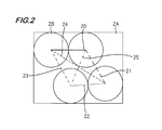
- FIG. 2 is a diagram when a partial region of the optical layer 2 is viewed from the light emitting layer 4 side, and is a diagram for explaining an interval between convex portions.
- the inventor has a particle size of the particle 2B of the optical layer 2 of 1000 nm or less, and furthermore, among the intervals between the convex portions formed on the surface of the optical layer 2, the most existing first length interval.
- the appearance frequency is “1”
- the particle diameter of the particle 2B is a diameter of a circle having a size corresponding to the area of the particle in plan view.
- the particle diameter of the particles 2B in the optical layer 2 is preferably in the range of 200 nm to 800 nm, and more preferably in the range of 300 nm to 600 nm.
- the appearance frequency is between the first length and the second length. It has been found that the light extraction efficiency can be further improved by the non-monotonic decrease.
- the above-mentioned intervals of all lengths included in the optical layer 2 can be measured by performing a fast Fourier transform (FFT) process on a microscope image obtained by imaging the surface of the optical layer 2 where the irregularities are formed with a laser microscope. It is.
- FFT fast Fourier transform
- the average height of the irregularities formed on the surface of the optical layer 2 is too large, the transparent electrode 3 formed on the optical layer 2. And a reflection electrode 5 leak.
- the average height of the unevenness formed on the surface of the optical layer 2 be 200 nm or less.
- the average height of the irregularities may be larger than 200 nm.
- the lower limit value of the average height of the irregularities may be about 20 nm as long as the irregularities to the extent that a diffraction phenomenon can be expected are formed.
- the average height of the unevenness means the average height from the bottom of the uneven concave portion to the top of the convex portion, and can be obtained, for example, as follows.
- the depth to the bottom of one recess is 1/2 of the sum of the distances from the tops of the two adjacent protrusions to the bottom of the recess. Therefore, for each of 10 or more randomly extracted recesses, the sum of the distances from the tops of the two adjacent protrusions to the bottom of the recesses was obtained, and 1/2 of each was further obtained.
- the average value is the average height.
- the optical layer 2 having the above-described configuration can be formed, for example, by applying a binder in which resin particles such as acrylic are dispersed to the transparent substrate 1.
- a suitable transparent resin is used as the material of the binder layer used for the optical layer 2.
- acrylic resin for example, acrylic resin, polyethylene, polypropylene, polyethylene terephthalate, polymethyl methacrylate (PMMA), polystyrene, polyethersulfone, polyarylate, polycarbonate resin, polyurethane, polyacrylonitrile, polyvinyl acetal, polyamide, polyimide, diester
- acrylic phthalate resins acrylic resins, cellulose resins, polyvinyl chloride, polyvinylidene chloride, polyvinyl acetate, other thermoplastic resins, and copolymers of two or more monomers constituting these resins.
- the optical layer 2 it is preferable to determine the relationship between the refractive index of the binder layer 2A and the refractive index of the particles 2B so that light incident from the transparent electrode 3 is not scattered inside.
- the refractive index of the optical layer 2 can be made substantially uniform. 2 can effectively prevent light scattering inside. As a result, the amount of light incident on the optical layer 2 returning to the light emitting layer 4 side by scattering can be reduced, and the light extraction efficiency of the organic EL element 100 can be increased.
- the binder layer 2B and the transparent substrate 1 have substantially the same refractive index.
- the transparent electrode 3 is an electrode made of a conductive material that can sufficiently transmit the light emitted from the light emitting layer 4 and has a sufficiently higher conductivity than the material contained in the light emitting layer 4.
- a conductive polymer such as ITO or PEDOT-PSS is used.
- Examples of the conductive polymer used for the transparent electrode 3 include, but are not limited to, conductive polymers such as polythiophene, polyaniline, polypyrrole, polyphenylene, polyphenylene vinylene, polyacetylene, polycarbazole, polyacetylene, and polyethylenedioxythiophene. It is not something. These may be used alone or in combination.
- the transparent electrode 3 has a shape reflecting the shape of the unevenness on the surface of the optical layer 2, and the surface on the light emitting layer 4 side of the transparent electrode 3 is the surface on the optical layer 2 side. Asperity is formed.
- unevenness having a shape reflecting the unevenness formed on the surface of the transparent electrode 3 on the light emitting layer 4 side is formed on the surface of the light emitting layer 4 on the reflective electrode 5 side.
- the surface of the light emitting layer 4 on the reflective electrode 5 side may be flat.
- the reflective electrode 5 is made of a conductive material that can reflect light emitted from the light emitting layer 4 and is sufficiently higher in conductivity than the material used for the light emitting layer 4.
- the reflective electrode 5 is made of, for example, aluminum or silver.
- Glass substrate surface treatment A glass substrate (Corning, Eagle XG, refractive index 1.51) is placed in a washing container, ultrasonically washed in a neutral detergent, then ultrasonically washed in pure water, and heated and dried at 120 ° C. for 120 minutes. went. The glass substrate was subjected to silane coupling treatment.
- TMPT made by Shin-Nakamura Chemical Co., Ltd.
- EA-200 made by Osaka Gas Chemical Co., Ltd.
- PGME propylene glycol monomethyl ether
- MEK methyl ethyl ketone
- the optical layer 2 is formed by applying the material liquid of the optical layer 2 to the glass substrate using a wire bar, and then curing by UV irradiation (365 nm) for 10 minutes.
- the number of the particles 2B included in the optical layer 2 thus formed is N, and the particles 2B when the particles 2B are arranged in a close-packed manner so that the particles 2B do not overlap in a plane region on the transparent substrate 1 on which the optical layer 2 is formed.
- N ⁇ ⁇ M ( ⁇ is a natural number of 1 or more)
- the particle density of the optical layer 2 is said to be ⁇ .
- the above-mentioned condition concerning the interval between the convex portions of the optical layer 2 can be realized by adjusting the particle diameter of the particles contained in the material liquid and the value of ⁇ .
- the particle density ⁇ is preferably 1.5 or more, and more preferably 2 or more.
- HATCN hexaazatriphenylene hexacarbonitrile
- ⁇ -NPD Bis [N- (1-naphthyl) -N-phenyl] benzidine
- an organic material A represented by the following structural formula is vacuum-deposited to a thickness of 5 nm to form a second hole transport layer.
- MCP metal-dicarbazo-9-rylbenzene
- a material doped with the light emitting material A is vacuum-deposited to a thickness of 30 nm to form an organic light emitting layer.
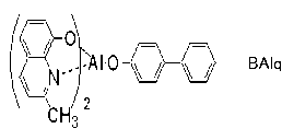
- BAlq (Bis- (2-methyl-8-quinolinolato) -4- (phenyl-phenolate) -aluminum (III)) represented by the following structural formula was vacuum-deposited to a thickness of 39 nm.
- the first electron transport layer is formed.
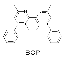
- BCP 2,9-dimethyl-4,7-diphenyl-1,10-phenanthroline represented by the following structural formula was vacuum-deposited so as to have a thickness of 1 nm.
- the electron transport layer is formed.
- LiF is deposited on the second electron transport layer so as to have a thickness of 1 nm to form an electron injection layer. Thereby, the formation of the light emitting layer 4 is completed.
- Aluminum is deposited on the electron injection layer to a thickness of 200 nm to form the reflective electrode 5.
- a constituent other than the transparent substrate 1 is sealed with a sealing glass can in which a desiccant is attached in a nitrogen gas atmosphere and a sealing material is applied to the installation surface with the transparent substrate.
- the optical layer can be formed by applying the material liquid as described above. Moreover, the space
- the organic EL element was manufactured by the said manufacturing method by making the particle size of the particle
- grains which comprise an optical layer into 300 nm, and setting the density (alpha) 2 of the particle
- the refractive index difference between the particles in the optical layer and the binder layer was set to 0.01 by adjusting the mixing ratio of the two binders contained in the binder layer material.
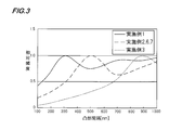
- the distribution of the convex portions of the optical layer was as shown in the graph of FIG. In the graph shown in FIG. 3, the horizontal axis indicates the interval between the convex portions, and the vertical axis indicates the appearance frequency for each interval between the convex portions as the relative frequency when the appearance frequency of the most existing interval is 1. ing.
- Example 2 An organic EL element was produced in the same manner as in Example 1 except that the particle size of the particles constituting the optical layer was 500 nm. In the element of Example 2, the distribution of the convex portions of the optical layer was as shown in FIG.
- Example 3 An organic EL device was produced in the same manner as in Example 1 except that the particle size of the particles constituting the optical layer was 800 nm. In the element of Example 3, the distribution of the convex portions of the optical layer was as shown in FIG.
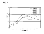
- Example 4 An organic EL element was produced in the same manner as in Example 1 except that the particle size of the particles constituting the optical layer was 500 nm and ⁇ was set to 3. In the element of Example 4, the distribution of the convex portions of the optical layer was as shown in FIG. The horizontal axis and horizontal axis of the graph shown in FIG. 4 are the same as those in FIG.
- Example 5 An organic EL element was produced in the same manner as in Example 1 except that the particle diameter of the particles constituting the optical layer was 500 nm and ⁇ was set to 4. In the element of Example 5, the distribution of the convex portions of the optical layer was as shown in FIG.
- Example 6 An organic EL device was produced in the same manner as in Example 1 except that the particle diameter of the particles constituting the optical layer was 500 nm and the material constituting the transparent electrode was changed to PEDOT-PSS. In the element of Example 6, the distribution of the convex portions of the optical layer was almost the same as that of the element of Example 2.
- Example 7 The organic EL element was fabricated in the same manner as in Example 1 except that the particle size of the particles constituting the optical layer was 500 nm and the refractive index difference between the particles in the optical layer and the binder layer was adjusted to 0.05. Produced. In the element of Example 7, the distribution of the convex portions of the optical layer was almost the same as that of the element of Example 2.
- Example 8 An organic EL element was produced in the same manner as in Example 1 except that the particle size of the particles constituting the optical layer was 500 nm and ⁇ was set to 1.5. In the element of Example 8, the distribution of the convex portions of the optical layer was as shown in FIG.
- ⁇ Comparative example 4> The organic EL device was prepared in the same manner as in Example 1 except that the particle size of the particles constituting the optical layer was 500 nm and the difference in refractive index between the particles in the optical layer and the binder layer was adjusted to 0.15. Produced. In the element of Comparative Example 4, the distribution of convex portions of the optical layer was as shown in FIG.
- the external quantum efficiency and the driving voltage were measured for each device thus fabricated.
- “C9920-12” manufactured by Hamamatsu Photonics was used, and the external quantum efficiency and the voltage value applied to the device when a current of 2.5 mA / cm 2 was passed through the device were read. Tables 1 and 2 below summarize the measurement results and device configuration.
- Examples 1, 2, 6, and 7 have higher quantum efficiencies than Examples 3 and 8. What is common to Examples 1, 2, 6, and 7 is that the relative frequency decreases non-monotonically from the interval at which the relative frequency becomes “1” to the interval of 1000 nm. Non-monotonic decrease means that the value does not continue to decrease, but increases or disappears along the way.
- the relative frequency monotonously decreases from the peak means that the interval with a high relative frequency becomes difficult to disperse in the wavelength range of 100 nn to 1000 nm. Therefore, by providing the optical layer with a distribution in which the relative frequency decreases non-monotonically, the light extraction efficiency can be further improved as can be seen from the results of Examples 1, 2, 6, and 7.
- the efficiency can be maximized when the particle diameter of the particles in the optical layer is in the range of 300 nm to 600 nm.
- the organic EL material used for the organic EL element has a refractive index as high as about 1.8, so that the wavelength range of visible light (380 nm to 780 nm) is 200 nm to 450 nm in this organic EL material.
- the optical layer has a particle size, the extraction efficiency in the entire visible light can be increased.
- the disclosed organic electroluminescent device is formed on a transparent substrate, an optical layer formed on the transparent substrate, having an uneven surface on the surface opposite to the transparent substrate and having a uniform refractive index, and the optical layer.
- the optical layer includes a binder layer and particles embedded in the binder layer. And the particle diameter of the particle is 1000 nm or less, and the interval between the convex portions on the surface of the optical layer varies in the range of 100 nm to 1000 nm, and the appearance of the interval that is most abundant in the optical layer. When the frequency is “1”, the appearance frequency of the above-mentioned interval of 1000 nm is 0.5 or more.
- the disclosed organic electroluminescence device has a frequency range from the most existing interval in the optical layer to the interval of 1000 nm when the appearance frequency is plotted for each interval of all the lengths included in the optical layer. In which the appearance frequency is non-monotonically decreasing.
- the number of the particles contained in the optical layer when the particles are arranged in a close-packed manner so that the particles do not overlap in a plane region where the optical layer is formed is Including those that are 1.5 times or more.
- the disclosed organic electroluminescent elements include those in which the particle diameter is in the range of 300 nm to 600 nm.
- the disclosed organic electroluminescent elements include those in which the difference in refractive index between the particles and the binder layer is 0.1 or less.
- the disclosed organic electroluminescent elements include those in which the average height of the irregularities is in the range of 20 nm to 200 nm.
Landscapes
- Physics & Mathematics (AREA)
- Optics & Photonics (AREA)
- Electroluminescent Light Sources (AREA)
Abstract
広帯域での光取り出し効率を向上させることのできる安価な有機電界発光素子を提供する。 有機EL素子100は、透明基板1上に形成され、透明基板1とは反対側の表面に凹凸を有する屈折率が均一な光学層2と、光学層2上に形成される透明電極3と、透明電極3上に形成される発光層4と、発光層4上に形成される反射電極5とを備える。光学層2は、バインダ層2Aと粒子2Bとにより構成される。粒子2Bの粒径は1000nm以下であり、光学層2の表面にある凸部同士の間隔は100nm~1000nmの範囲でばらついている。光学層2において最も多く存在する上記間隔の出現頻度を"1"としたとき、1000nmの上記間隔の出現頻度が0.5以上である。
Description
本発明は、有機電界発光(EL:エレクトロルミネセンス)素子に関する。
有機EL素子は、透明基板上に、透明電極と、発光層と、反射電極とをこの順に積層した構造が一般的である。
このような有機EL素子において、透明基板からの光取り出し効率を高めるための様々な工夫がなされている。
例えば、特許文献1~4には、透明基板と透明電極の間の界面にランダムな凹凸を設けることで、広い波長領域での光取り出し効率を向上させた有機EL素子が記載されている。
特許文献1~4には、透明基板と透明電極の間の界面に設ける凹凸の間隔を、どの程度ランダムにすれば光取り出し効率を向上させられるかについては考慮されていない。また、金型等を用いて凹凸を形成しているため、凹凸の間隔を細かく制御することが難しく、製造コストが高くなる。
本発明の目的は、広い波長領域での光取り出し効率を向上させることのできる安価な有機電界発光素子を提供することにある。
本発明の有機電界発光素子は、透明基板と、上記透明基板上に形成され、上記透明基板とは反対側の表面に凹凸を有する屈折率が均一な光学層と、上記光学層上に形成される透明電極と、上記透明電極上に形成される発光層と、上記発光層上に形成される反射電極と、を備え、上記光学層は、バインダ層と、上記バインダ層に埋められる粒子とにより構成され、上記粒子の粒径は1000nm以下であり、上記光学層の表面にある凸部同士の間隔は、100nm~1000nmの範囲でばらついており、上記光学層において最も多く存在する上記間隔の出現頻度を“1”としたとき、1000nmの上記間隔の出現頻度が0.5以上であるものである。
本発明によれば、広い波長領域での光取り出し効率を向上させることのできる安価な有機電界発光素子を提供することができる。
以下、本発明の実施形態について図面を参照して説明する。
図1は、本発明の一実施形態を説明するための有機EL素子の断面構成を示す図である。
有機EL素子100は、透明基板1と、透明基板1上に形成された透明基板1側の表面に凹凸を有する屈折率が均一な光学層2と、光学層2上に形成された透明電極3と、透明電極3上に形成された、有機又は無機の発光材料からなる有機発光層又は無機発光層を含む発光層4と、発光層4上に形成された反射電極5と、を備える。光学層2と透明電極3の間には補助配線があってもよい。発光層4は、必要に応じて正孔注入層、正孔輸送層、電子注入層、電子輸送層等を含んでいてもよい。
透明電極3と反射電極5のうち、一方は陽極、他方は陰極である。これら陽極と陰極との間に直流電圧を印加すると、陰極及び陽極から発光層4に含まれる有機発光層又は無機発光層に電子及び正孔が注入され、それらの再結合によって励起子が生成され、この励起子が失活する際の光の放出により、発光層4が発光する。発光層4から発せられた光を透明基板1側に取り出すことで、有機EL素子100を照明や表示素子等に利用することができる。本実施形態では、発光層4として白色光を発光するものを用いる。
透明基板1は、発光層4から発せられる光を十分に透過できる材料で構成されたものであればよく、例えばガラス基板、樹脂基板等が用いられる。
光学層2は、光の回折現象により、透明基板1側に取り出すことのできる光を増やすために設けられる。
光学層2は、バインダ層2Aと、バインダ層2Aに埋められた多数の粒子2Bとにより構成される。この多数の粒子2Bにより、光学層2の透明基板1とは反対側の表面に凹凸が形成される。粒子2Bは、図1では球状としているが、三角柱、四角柱等、様々な形状のものが用いられる。
光学層2の表面にある凹凸の凸部同士の間隔は、可視光の波長域(一般的には380nm~780nm)を含みかつこの波長域よりも広い波長範囲でばらついている。このように、回折格子の格子間隔に相当する凸部同士の間隔がばらついていることで、可視光の波長域のうちの特定波長の光のみでなく、この波長域にある多くの波長の光で、光取り出し効率を向上させることが可能となる。
なお、上記波長範囲は、可視光の種々の波長において光取り出し効率を高めるために、100nm~1000nmの範囲としておくのがよい。
凸部同士の間隔は、光学層2の表面に形成される全ての凸部と、この全ての凸部の各々に隣接する他の凸部との間隔のことを言う。ここで、隣接する2つの凸部とは、この2つの凸部の頂部同士を結ぶ直線上に、この2つの凸部以外の別の凸部が配置されないもののことを言う。
図2は、光学層2の一部領域を発光層4側から見たときの図であり、凸部同士の間隔を説明するための図である。図2に示す一部領域には、上記定義にしたがい、凸部の間隔として、符号20,21,22,23,24,25で示す6つの間隔が存在する。
発明者は、光学層2の粒子2Bの粒径が1000nm以下であり、更に、光学層2の表面に形成される凸部同士の間隔のうち、最も多く存在する第一の長さの間隔の出現頻度を “1”としたとき、上記波長範囲における長波長側の端部の波長と同じ第二の長さ(=1000nm)の間隔の出現頻度が0.5以上となっていることで、凸部同士の間隔を単にランダムにする場合と比較して、光取り出し効率を向上させられることを見出した。
なお、粒子2Bの粒径とは、粒子の平面視における面積に相当する大きさの円の直径である。光学層2における粒子2Bの粒径は200nm~800nmの範囲であることが好ましく、300nm~600nmの範囲であることがより好ましい。
更に、発明者は、光学層2に含まれる全ての長さの上記間隔毎にその出現頻度をプロットした場合に、上記第一の長さから上記第二の長さの間において、出現頻度が非単調減少となっていることで、光取り出し効率を更に向上させられることを見出した。
光学層2に含まれる全ての長さの上記間隔は、光学層2の凹凸が形成される面をレーザー顕微鏡によって撮像して得た顕微鏡画像に高速フーリエ変換(FFT)処理を行うことで測定可能である。
ここまでは、光学層2の凸部同士の間隔の条件について説明したが、光学層2の表面に形成される凹凸の平均高さが大きすぎると、光学層2上に形成される透明電極3と反射電極5との間でリークが発生してしまう。このため、光学層2の表面に形成される凹凸の平均高さは200nm以下にすることが好ましい。もちろん、リーク対策を他の手段(発光層4を平坦にする等)で行えば、凹凸の平均高さは200nmより大きくしても構わない。凹凸の平均高さの下限値は、回折現象が期待できる程度の凹凸が形成されればよく、20nm程度としておくのがよい。
なお、凹凸の平均高さは、凹凸の凹部の底部から凸部の頂部までの高さの平均のことを意味し、例えば次のようにして求めることができる。
凹凸パターンを原子間力顕微鏡などにより観察し、その観察から表面微細凹凸体の断面図を得る。1つの凹部の底までの深さは、両隣の2つの凸部の頂部から凹部の底までの距離の和の1/2である。そこで、無作為に抽出した10個以上の各凹部について、このように両隣の2つの凸部の頂部から凹部の底までの距離の和を求め、更にその1/2をそれぞれ求め、得られた値の平均値を平均高さとする。
以上のような構成の光学層2は、例えば、アクリル等の樹脂製の粒子を分散させたバインダを透明基板1に塗布することによって形成することができる。
光学層2に用いられるバインダ層の材料としては、透明性のある適宜の樹脂が用いられる。
この樹脂としては、例えば、アクリル樹脂、ポリエチレン、ポリプロピレン、ポリエチレンテレフタレート、ポリメチルメタクリレート(PMMA)、ポリスチレン、ポリエーテルスルホン、ポリアリレート、ポリカーボネート樹脂、ポリウレタン、ポリアクリルニトリル、ポリビニルアセタール、ポリアミド、ポリイミド、ジアクリルフタレート樹脂、セルロース系樹脂、ポリ塩化ビニル、ポリ塩化ビニリデン、ポリ酢酸ビニル、その他の熱可塑性樹脂や、これらの樹脂を構成する単量体の2種以上の共重合体等が挙げられる。
光学層2は、透明電極3から入射する光が内部において散乱しないように、バインダ層2Aの屈折率と粒子2Bの屈折率との関係を定めておくのがよい。
バインダ層2Aの屈折率と粒子2Bの屈折率の差を0.1以下、好ましくは0.05以下とすることで、光学層2の屈折率を実質的に均一にすることができ、光学層2内部での光の散乱を効果的に防ぐことができる。この結果、光学層2に入射した光が散乱によって発光層4側に戻る量を減らすことができ、有機EL素子100の光取り出し効率を高くすることができる。
また、光学層2と透明基板1との界面での光の散乱を防ぐためにも、バインダ層2Bと透明基板1とはほぼ同じ屈折率にしておくことが好ましい。
透明電極3は、発光層4から発せられる光を十分に透過でき、かつ、発光層4に含まれる材料よりも導電性が十分に高い導電性材料で構成された電極である。透明電極3の材料には、例えばITOや、PEDOT-PSS等の導電性高分子が用いられる。
透明電極3に用いられる導電性高分子としては、ポリチオフェン、ポリアニリン、ポリピロール、ポリフェニレン、ポリフェニレンビニレン、ポリアセチレン、ポリカルバゾール、ポリアセチレン、ポリエチレンジオキシチオフェン等の導電性高分子が挙げられるが、これらに限定されるものではない。また、これらを単独で用いてもよいし、組み合わせて用いてもよい。
図1に示すように、透明電極3は、光学層2の表面にある凹凸の形状を反映した形状となっており、透明電極3の発光層4側の表面には、光学層2側の表面と同等の凹凸が形成される。
図1では、発光層4の反射電極5側の面には、透明電極3の発光層4側の面に形成された凹凸を反映した形状の凹凸が形成されている。しかし、発光層4の反射電極5側の面は、平坦であってもよい。
反射電極5は、発光層4から発せられる光を反射することができ、かつ、発光層4に用いられる材料よりも導電性の十分に高い導電性材料で構成される。反射電極5は、例えばアルミニウム、銀等が用いられる。
次に、有機EL素子100の製造方法の一例を説明する。
(ガラス基板表面処理)
ガラス基板(コーニング社製、Eagle XG、屈折率1.51)を洗浄容器に入れ、中性洗剤中で超音波洗浄した後、純水中で超音波洗浄し、120℃で120分間加熱乾燥を行った。ガラス基板はシランカップリング処理を行った。
ガラス基板(コーニング社製、Eagle XG、屈折率1.51)を洗浄容器に入れ、中性洗剤中で超音波洗浄した後、純水中で超音波洗浄し、120℃で120分間加熱乾燥を行った。ガラス基板はシランカップリング処理を行った。
(光学層形成工程)
バインダとしてTMPT(新中村化学工業株式会社製)2500mg及びEA-200(大阪ガスケミカル株式会社製)650mgと、溶媒としてPGME(プロピレングリコールモノメチルエーテル)12000mg及びMEK(メチルエチルケトン)4500mgとを、ローラー、スターラーにより攪拌し、十分に混合させてバインダ層材料液を形成する。
バインダとしてTMPT(新中村化学工業株式会社製)2500mg及びEA-200(大阪ガスケミカル株式会社製)650mgと、溶媒としてPGME(プロピレングリコールモノメチルエーテル)12000mg及びMEK(メチルエチルケトン)4500mgとを、ローラー、スターラーにより攪拌し、十分に混合させてバインダ層材料液を形成する。
次に、このバインダ層材料液に対し、架橋アクリル系粒子(テクポリマー(積水化成品工業株式会社製、登録商標))合計4500mgと、重合開始剤(BASFジャパン社製)30mgを添加し、スターラーにて攪拌して光学層2の材料液を形成する。
ガラス基板にワイヤーバーを用いて上記光学層2の材料液を塗布し、その後、UV照射(365nm)を10分間行い硬化させて、光学層2を形成する。
こうしてできた光学層2に含まれる粒子2Bの数をNとし、光学層2が形成される透明基板1上の平面領域内に粒子2Bが重ならないように最密に配置したときの粒子2Bの数をMとしたとき、N=α×M(αは1以上の自然数)である場合、光学層2の粒子密度はαであるという。
光学層2の凸部同士の間隔に関する上記条件は、材料液に含まれる粒子の粒径と上記αの値とを調整することで実現可能である。粒子密度αは1.5以上が好ましく、2以上がより好ましい。
(透明電極形成工程)
光学層2上に、補助配線としてAgを100nm、金属マスクを介して成膜し、その後、ITOを真空蒸着装置によってスパッタ蒸着して透明電極3を形成する。
光学層2上に、補助配線としてAgを100nm、金属マスクを介して成膜し、その後、ITOを真空蒸着装置によってスパッタ蒸着して透明電極3を形成する。
(発光層形成工程)
透明電極3上に、HATCN(ヘキサアザトリフェニレン ヘキサカルボニトリル)を厚み10nmとなるように真空蒸着して正孔注入層を形成する。
透明電極3上に、HATCN(ヘキサアザトリフェニレン ヘキサカルボニトリル)を厚み10nmとなるように真空蒸着して正孔注入層を形成する。
正孔注入層上に、α-NPD(Bis[N-(1-naphthyl)-N-phenyl]benzidine)を厚み500nmとなるように真空蒸着して、第一の正孔輸送層を形成する。
第一の正孔輸送層上に、下記構造式で表される有機材料Aを厚み5nmとなるように真空蒸着して、第二の正孔輸送層を形成する。

次に、第二の正孔輸送層上に、MCP(メタ-ジカルバゾ-9-リ ルベンゼン)をホスト材料として、このホスト材料に対して40質量%の燐光発光材料である下記構造式で表される発光材料Aをドープした材料を厚み30nmとなるように真空蒸着して、有機発光層を形成する。
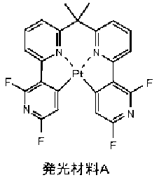
有機発光層上に、下記構造式で表されるBAlq(Bis-(2-methyl-8-quinolinolato)-4-(phenyl-phenolate)-aluminium(III))を厚み39nmとなるように真空蒸着して、第一の電子輸送層を形成する。
第一の電子輸送層上に、下記構造式で表されるBCP(2,9-ジメチル-4,7-ジフェニル-1,10-フェナントロリン)を厚み1nmとなるように真空蒸着して、第二の電子輸送層を形成する。
第二の電子輸送層上にLiFを厚み1nmとなるように蒸着して電子注入層を形成する。これにより、発光層4の形成を終了する。
(反射電極形成工程)
電子注入層の上にアルミニウムを厚み200nmとなるように蒸着して、反射電極5を形成する。
電子注入層の上にアルミニウムを厚み200nmとなるように蒸着して、反射電極5を形成する。
(封止工程)
窒素ガス雰囲気中にて乾燥剤を貼り付け、透明基板との設置面に封止材を塗った封止ガラス缶にて、透明基板1以外の構成要素を封止する。
窒素ガス雰囲気中にて乾燥剤を貼り付け、透明基板との設置面に封止材を塗った封止ガラス缶にて、透明基板1以外の構成要素を封止する。
有機EL素子100によれば、上記のように、材料液の塗布によって光学層を形成することができる。また、光学層の凸部同士の間隔を、粒子の粒径や密度によって容易に調整することができる。したがって、製造コストを増大させることなく、光取り出し効率を向上させることができる。
次に、上記構成の有機EL素子100において光取出し効率を検証した結果を以下に説明する。
<実施例1>
光学層を構成する粒子の粒径を300nmとし、光学層における粒子の密度α=2として、上記製造方法により有機EL素子を製造した。実施例1の素子では、バインダ層材料に含まれる2つのバインダの混合比を調整することで、光学層における粒子とバインダ層との屈折率差を0.01にした。実施例1の素子は、光学層の凸部の分布が図3のグラフに示すようなものとなった。図3に示すグラフは、横軸に凸部同士の間隔を示し、縦軸に、凸部の間隔毎の出現頻度を、最も多く存在する間隔の出現頻度を1としたときの相対頻度として示している。
光学層を構成する粒子の粒径を300nmとし、光学層における粒子の密度α=2として、上記製造方法により有機EL素子を製造した。実施例1の素子では、バインダ層材料に含まれる2つのバインダの混合比を調整することで、光学層における粒子とバインダ層との屈折率差を0.01にした。実施例1の素子は、光学層の凸部の分布が図3のグラフに示すようなものとなった。図3に示すグラフは、横軸に凸部同士の間隔を示し、縦軸に、凸部の間隔毎の出現頻度を、最も多く存在する間隔の出現頻度を1としたときの相対頻度として示している。
<実施例2>
光学層を構成する粒子の粒径を500nmとした以外は、実施例1と同様の方法で有機EL素子を作製した。実施例2の素子は、光学層の凸部の分布が図3に示すようなものとなった。
光学層を構成する粒子の粒径を500nmとした以外は、実施例1と同様の方法で有機EL素子を作製した。実施例2の素子は、光学層の凸部の分布が図3に示すようなものとなった。
<実施例3>
光学層を構成する粒子の粒径を800nmとした以外は、実施例1と同様の方法で有機EL素子を作製した。実施例3の素子は、光学層の凸部の分布が図3に示すようなものとなった。
光学層を構成する粒子の粒径を800nmとした以外は、実施例1と同様の方法で有機EL素子を作製した。実施例3の素子は、光学層の凸部の分布が図3に示すようなものとなった。
<実施例4>
光学層を構成する粒子の粒径を500nmとし、α=3とした以外は、実施例1と同様の方法で有機EL素子を作製した。実施例4の素子は、光学層の凸部の分布が図4に示すようなものとなった。図4に示すグラフの横軸及び横軸は図3と同じである。
光学層を構成する粒子の粒径を500nmとし、α=3とした以外は、実施例1と同様の方法で有機EL素子を作製した。実施例4の素子は、光学層の凸部の分布が図4に示すようなものとなった。図4に示すグラフの横軸及び横軸は図3と同じである。
<実施例5>
光学層を構成する粒子の粒径を500nmとし、α=4とした以外は、実施例1と同様の方法で有機EL素子を作製した。実施例5の素子は、光学層の凸部の分布が図4に示すようなものとなった。
光学層を構成する粒子の粒径を500nmとし、α=4とした以外は、実施例1と同様の方法で有機EL素子を作製した。実施例5の素子は、光学層の凸部の分布が図4に示すようなものとなった。
<実施例6>
光学層を構成する粒子の粒径を500nmとし、透明電極を構成する材料をPEDOT-PSSに変更した以外は、実施例1と同様の方法で有機EL素子を作製した。実施例6の素子は、光学層の凸部の分布が、実施例2の素子とほぼ同じになった。
光学層を構成する粒子の粒径を500nmとし、透明電極を構成する材料をPEDOT-PSSに変更した以外は、実施例1と同様の方法で有機EL素子を作製した。実施例6の素子は、光学層の凸部の分布が、実施例2の素子とほぼ同じになった。
<実施例7>
光学層を構成する粒子の粒径を500nmとし、光学層における粒子とバインダ層との屈折率差が0.05となるように調整した以外は、実施例1と同様の方法で有機EL素子を作製した。実施例7の素子は、光学層の凸部の分布が、実施例2の素子とほぼ同じになった。
光学層を構成する粒子の粒径を500nmとし、光学層における粒子とバインダ層との屈折率差が0.05となるように調整した以外は、実施例1と同様の方法で有機EL素子を作製した。実施例7の素子は、光学層の凸部の分布が、実施例2の素子とほぼ同じになった。
<実施例8>
光学層を構成する粒子の粒径を500nmとし、α=1.5とした以外は、実施例1と同様の方法で有機EL素子を作製した。実施例8の素子は、光学層の凸部の分布が図4に示すようなものとなった。
光学層を構成する粒子の粒径を500nmとし、α=1.5とした以外は、実施例1と同様の方法で有機EL素子を作製した。実施例8の素子は、光学層の凸部の分布が図4に示すようなものとなった。
<比較例1>
光学層を省略した以外は、実施例1と同様の方法で有機EL素子を作製した。
光学層を省略した以外は、実施例1と同様の方法で有機EL素子を作製した。
<比較例2>
光学層を構成する粒子の粒径を500nmとし、α=1とした以外は、実施例1と同様の方法で有機EL素子を作製した。比較例2の素子は、光学層の凸部の分布が図5に示すようなものとなった。図5に示すグラフの横軸及び横軸は図3と同じである。
光学層を構成する粒子の粒径を500nmとし、α=1とした以外は、実施例1と同様の方法で有機EL素子を作製した。比較例2の素子は、光学層の凸部の分布が図5に示すようなものとなった。図5に示すグラフの横軸及び横軸は図3と同じである。
<比較例3>
光学層を構成する粒子の粒径を1500nmとした以外は、実施例1と同様の方法で有機EL素子を作製した。比較例3の素子は、光学層の凸部の分布が図5に示すようなものとなった。
光学層を構成する粒子の粒径を1500nmとした以外は、実施例1と同様の方法で有機EL素子を作製した。比較例3の素子は、光学層の凸部の分布が図5に示すようなものとなった。
<比較例4>
光学層を構成する粒子の粒径を500nmとし、光学層における粒子とバインダ層との屈折率差が0.15となるように調整した以外は、実施例1と同様の方法で有機EL素子を作製した。比較例4の素子は、光学層の凸部の分布が図5に示すようなものとなった。
光学層を構成する粒子の粒径を500nmとし、光学層における粒子とバインダ層との屈折率差が0.15となるように調整した以外は、実施例1と同様の方法で有機EL素子を作製した。比較例4の素子は、光学層の凸部の分布が図5に示すようなものとなった。
このようにして作製した各素子について、外部量子効率と駆動電圧を測定した。外部量子効率と駆動電圧は、浜松ホトニクス製「C9920-12」を用い、2.5mA/cm2の電流を素子に流したときの外部量子効率と素子に加わった電圧値を読みとった。測定結果と素子構成をまとめたものを、以下の表1,2に示す。

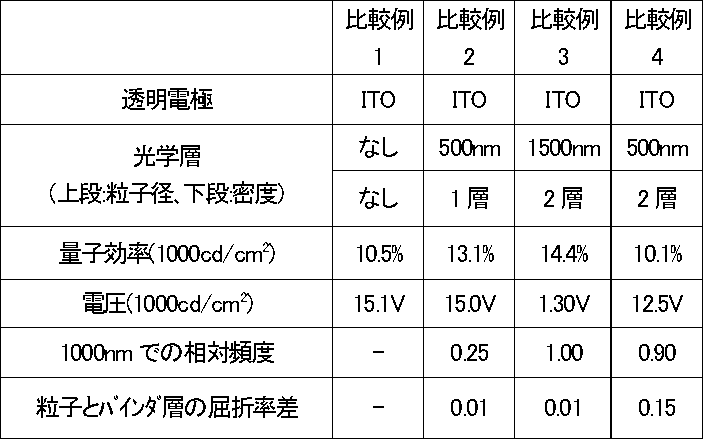
実施例1~8と比較例2との比較により、間隔=1000nmにおける相対頻度が0.5以上になっていると、量子効率が高くなることがわかる。
また、比較例3は、間隔=1000nmにおける相対頻度が1であり、間隔=1000nmにおける相対頻度が0.5以上という要件を満たしているが、量子効率は14.4%と低い。これは、粒子の粒径が1500nmと大きいために、相対頻度の高い間隔が長波長側に偏ることで、量子効率が落ちるためと考えられる。実施例1~8のように、粒径を1000nm以下とすることで、相対頻度の高い間隔が、100nn~1000nmの波長範囲で分散することになり、量子効率を高めることができる。
また、比較例4は、間隔=1000nmにおける相対頻度が0.9であるが、量子効率は10.1%と低い。これは、光学層において粒子とバインダ層の屈折率差が大きく、光学層内において光の散乱が生じてしまっているためと考えられる。実施例1~8と比較例4の結果から、光学層において粒子とバインダ層の屈折率差が0.1以下となっていることで、量子効率の低下を防げることが分かる。
また、実施例1,2,6,7は、実施例3,8と比べると量子効率が高くなっている。実施例1,2,6,7に共通するのは、相対頻度が“1”になる間隔から1000nmの間隔までの間において、相対頻度が非単調減少となっていることである。非単調減少とは、値が下がり続けるのではなく、途中で上がったり、途中で変化がなくなったりすることを言う。
相対頻度がピークから単調減少するということは、相対頻度の高い間隔が100nn~1000nmの波長範囲で分散しにくくなることを意味する。したがって、相対頻度が非単調減少になる分布を光学層に持たせることで、実施例1,2,6,7の結果からも分かるように、光取り出し効率をより向上させることができる。
また、実施例1,2,3,6,7の結果から、光学層の粒子の粒径は、300nm~600nmの範囲にあれば、最も効率を上げられることがわかる。これは、有機EL素子に用いる有機EL材料は、屈折率が1.8程度と高いため、可視光(380nm~780nm)の波長範囲が、この有機EL材料中では波長200nm~450nmとなり、この範囲に光学層の粒径があれば、可視光全体での取り出し効率を挙げられるためである。
以上説明してきたように、本明細書には以下の事項が開示されている。
開示された有機電界発光素子は、透明基板と、上記透明基板上に形成され、上記透明基板とは反対側の表面に凹凸を有する屈折率が均一な光学層と、上記光学層上に形成される透明電極と、上記透明電極上に形成される発光層と、上記発光層上に形成される反射電極と、を備え、上記光学層は、バインダ層と、上記バインダ層に埋められる粒子とにより構成され、上記粒子の粒径は1000nm以下であり、上記光学層の表面にある凸部同士の間隔は、100nm~1000nmの範囲でばらついており、上記光学層において最も多く存在する上記間隔の出現頻度を“1”としたとき、1000nmの上記間隔の出現頻度が0.5以上であるものである。
開示された有機電界発光素子は、上記光学層に含まれる全ての長さの上記間隔毎に出現頻度をプロットした場合に、上記光学層において最も多く存在する上記間隔から1000nmの上記間隔までの間において、上記出現頻度が非単調減少となっているものを含む。
開示された有機電界発光素子は、上記光学層に含まれる上記粒子の数が、上記光学層が形成される平面領域内に上記粒子が重ならないように最密に配置したときの上記粒子の数の1.5倍以上となっているものを含む。
開示された有機電界発光素子は、上記粒子の粒径が、300nm~600nmの範囲にあるものを含む。
開示された有機電界発光素子は、上記粒子と上記バインダ層との屈折率の差が0.1以下であるものを含む。
開示された有機電界発光素子は、上記凹凸の平均高さが20nm~200nmの範囲にあるものを含む。
本発明によれば、広い波長領域での光取り出し効率を向上させることのできる安価な有機電界発光素子を提供することができる。
以上、本発明を特定の実施形態によって説明したが、本発明はこの実施形態に限定されるものではなく、開示された発明の技術思想を逸脱しない範囲で種々の変更が可能である。
本出願は、2013年3月25日出願の日本特許出願(特願2013-062199)に基づくものであり、その内容はここに取り込まれる。
本出願は、2013年3月25日出願の日本特許出願(特願2013-062199)に基づくものであり、その内容はここに取り込まれる。
100 有機EL素子
1 透明基板
2 光学層
2A バインダ層
2B 粒子
3 透明電極
4 発光層
5 反射電極
1 透明基板
2 光学層
2A バインダ層
2B 粒子
3 透明電極
4 発光層
5 反射電極
Claims (6)
- 透明基板と、
前記透明基板上に形成され、前記透明基板とは反対側の表面に凹凸を有する屈折率が均一な光学層と、
前記光学層上に形成される透明電極と、
前記透明電極上に形成される発光層と、
前記発光層上に形成される反射電極と、を備え、
前記光学層は、バインダ層と、前記バインダ層に埋められる粒子とにより構成され、
前記粒子の粒径は1000nm以下であり、
前記光学層の表面にある凸部同士の間隔は、100nm~1000nmの範囲でばらついており、
前記光学層において最も多く存在する前記間隔の出現頻度を“1”としたとき、1000nmの前記間隔の出現頻度が0.5以上である有機電界発光素子。 - 請求項1記載の有機電界発光素子であって、
前記光学層に含まれる全ての前記間隔毎に出現頻度をプロットした場合に、前記光学層において最も多く存在する前記間隔から1000nmの前記間隔までの間において、前記出現頻度が非単調減少となっている有機電界発光素子。 - 請求項1又は2記載の有機電界発光素子であって、
前記光学層に含まれる前記粒子の数が、前記光学層が形成される平面領域内に前記粒子が重ならないように最密に配置したときの前記粒子の数の1.5倍以上となっている有機電界発光素子。 - 請求項1~3のいずれか1項記載の有機電界発光素子であって、
前記粒子の粒径は、300nm~600nmの範囲にある有機電界発光素子。 - 請求項1~4のいずれか1項記載の有機電界発光素子であって、
前記粒子と前記バインダ層との屈折率の差は0.1以下である有機電界発光素子。 - 請求項1~5のいずれか1項記載の有機電界発光素子であって、
前記凹凸の平均高さは20nm~200nmの範囲にある有機電界発光素子。
Applications Claiming Priority (2)
| Application Number | Priority Date | Filing Date | Title |
|---|---|---|---|
| JP2013-062199 | 2013-03-25 | ||
| JP2013062199A JP5938363B2 (ja) | 2013-03-25 | 2013-03-25 | 有機電界発光素子 |
Publications (1)
| Publication Number | Publication Date |
|---|---|
| WO2014156405A1 true WO2014156405A1 (ja) | 2014-10-02 |
Family
ID=51623404
Family Applications (1)
| Application Number | Title | Priority Date | Filing Date |
|---|---|---|---|
| PCT/JP2014/054217 Ceased WO2014156405A1 (ja) | 2013-03-25 | 2014-02-21 | 有機電界発光素子 |
Country Status (2)
| Country | Link |
|---|---|
| JP (1) | JP5938363B2 (ja) |
| WO (1) | WO2014156405A1 (ja) |
Cited By (3)
| Publication number | Priority date | Publication date | Assignee | Title |
|---|---|---|---|---|
| WO2016174950A1 (ja) * | 2015-04-28 | 2016-11-03 | コニカミノルタ株式会社 | 有機エレクトロルミネッセンス素子 |
| CN106711347A (zh) * | 2016-12-28 | 2017-05-24 | 武汉华星光电技术有限公司 | 一种oled器件及其基板 |
| CN109545430A (zh) * | 2017-09-22 | 2019-03-29 | 南昌欧菲显示科技有限公司 | 透明导电性薄膜、触控屏及其制备方法 |
Families Citing this family (2)
| Publication number | Priority date | Publication date | Assignee | Title |
|---|---|---|---|---|
| CN104701466B (zh) * | 2015-03-25 | 2018-09-04 | 京东方科技集团股份有限公司 | 阵列基板及其制备方法和显示装置 |
| CN105977393B (zh) * | 2016-05-27 | 2019-03-08 | 纳晶科技股份有限公司 | 一种电致发光器件及其制作方法 |
Citations (4)
| Publication number | Priority date | Publication date | Assignee | Title |
|---|---|---|---|---|
| JP2006210204A (ja) * | 2005-01-31 | 2006-08-10 | Dainippon Printing Co Ltd | 反射性の改善された背面用基板およびこれを用いたディスプレイ |
| JP2010186613A (ja) * | 2009-02-12 | 2010-08-26 | Hitachi Displays Ltd | 有機発光素子及びその作製方法、並びに表示装置 |
| JP2011243290A (ja) * | 2010-05-14 | 2011-12-01 | Hitachi Ltd | 有機発光ダイオード及びこれを用いた光源装置 |
| WO2011148823A1 (ja) * | 2010-05-26 | 2011-12-01 | コニカミノルタホールディングス株式会社 | 光取り出しシート、有機エレクトロルミネッセンス素子及び照明装置 |
-
2013
- 2013-03-25 JP JP2013062199A patent/JP5938363B2/ja not_active Expired - Fee Related
-
2014
- 2014-02-21 WO PCT/JP2014/054217 patent/WO2014156405A1/ja not_active Ceased
Patent Citations (4)
| Publication number | Priority date | Publication date | Assignee | Title |
|---|---|---|---|---|
| JP2006210204A (ja) * | 2005-01-31 | 2006-08-10 | Dainippon Printing Co Ltd | 反射性の改善された背面用基板およびこれを用いたディスプレイ |
| JP2010186613A (ja) * | 2009-02-12 | 2010-08-26 | Hitachi Displays Ltd | 有機発光素子及びその作製方法、並びに表示装置 |
| JP2011243290A (ja) * | 2010-05-14 | 2011-12-01 | Hitachi Ltd | 有機発光ダイオード及びこれを用いた光源装置 |
| WO2011148823A1 (ja) * | 2010-05-26 | 2011-12-01 | コニカミノルタホールディングス株式会社 | 光取り出しシート、有機エレクトロルミネッセンス素子及び照明装置 |
Cited By (3)
| Publication number | Priority date | Publication date | Assignee | Title |
|---|---|---|---|---|
| WO2016174950A1 (ja) * | 2015-04-28 | 2016-11-03 | コニカミノルタ株式会社 | 有機エレクトロルミネッセンス素子 |
| CN106711347A (zh) * | 2016-12-28 | 2017-05-24 | 武汉华星光电技术有限公司 | 一种oled器件及其基板 |
| CN109545430A (zh) * | 2017-09-22 | 2019-03-29 | 南昌欧菲显示科技有限公司 | 透明导电性薄膜、触控屏及其制备方法 |
Also Published As
| Publication number | Publication date |
|---|---|
| JP5938363B2 (ja) | 2016-06-22 |
| JP2014186925A (ja) | 2014-10-02 |
Similar Documents
| Publication | Publication Date | Title |
|---|---|---|
| KR101330461B1 (ko) | 유기 전계 발광 장치, 표시 장치 및 조명 장치 | |
| JP5849087B2 (ja) | 発光デバイスおよび物品 | |
| JP5830194B2 (ja) | 有機エレクトロルミネッセンス素子及びそれを用いた照明装置 | |
| US8653548B2 (en) | Light-emitting device | |
| US8089208B2 (en) | Planar light source device | |
| JP6471905B2 (ja) | 発光装置 | |
| KR102163400B1 (ko) | 향상된 oled 어레이로부터의 광 아웃커플링을 위한 마이크로렌즈 어레이 구조물 | |
| JP5938363B2 (ja) | 有機電界発光素子 | |
| US8410477B2 (en) | Organic light emitting device, lighting apparatus and organic light emitting display apparatus | |
| CN103250265B (zh) | 有机电致发光元件 | |
| KR20160070142A (ko) | 유기 전계 발광 소자, 조명 장치 및 표시 장치 | |
| JP5763517B2 (ja) | 有機el素子 | |
| KR102283499B1 (ko) | Oled 구조 | |
| US9882170B2 (en) | Organic light emitting device with improved light extraction | |
| JP2012178279A (ja) | 有機エレクトロルミネッセンス素子 | |
| JP5827934B2 (ja) | 有機電界発光素子 | |
| JP6471907B2 (ja) | 発光装置 | |
| Peng et al. | Improving light extraction of organic light‐emitting devices by attaching nanostructures with self‐assembled photonic crystal patterns | |
| JP2013175403A (ja) | 有機エレクトロルミネッセンス素子 | |
| JP2015118863A (ja) | 発光素子及びそれを用いた照明装置 | |
| KR20140098687A (ko) | 광추출 향상층의 제조방법, 이에 따라 제조된 광추출 향상층을 포함하는 유기 발광 소자 및 이를 포함하는 조명 및 디스플레이 장치 | |
| WO2017213262A1 (ja) | 有機el素子、並びに有機el素子を利用した照明装置、面状光源及び表示装置 | |
| JP2011029120A (ja) | 発光装置 | |
| So et al. | Manufacturable Corrugated Substrates for High Efficiency Organic Light-Emitting Diodes (OLEDs) | |
| US20160111687A1 (en) | Organic light emitting diode structure and method of forming same |
Legal Events
| Date | Code | Title | Description |
|---|---|---|---|
| 121 | Ep: the epo has been informed by wipo that ep was designated in this application |
Ref document number: 14772655 Country of ref document: EP Kind code of ref document: A1 |
|
| NENP | Non-entry into the national phase |
Ref country code: DE |
|
| 122 | Ep: pct application non-entry in european phase |
Ref document number: 14772655 Country of ref document: EP Kind code of ref document: A1 |