WO2014136860A1 - 化合物、発光材料および有機発光素子 - Google Patents
化合物、発光材料および有機発光素子 Download PDFInfo
- Publication number
- WO2014136860A1 WO2014136860A1 PCT/JP2014/055720 JP2014055720W WO2014136860A1 WO 2014136860 A1 WO2014136860 A1 WO 2014136860A1 JP 2014055720 W JP2014055720 W JP 2014055720W WO 2014136860 A1 WO2014136860 A1 WO 2014136860A1
- Authority
- WO
- WIPO (PCT)
- Prior art keywords
- group
- substituted
- general formula
- compound
- light emitting
- Prior art date
Links
- HMXXDSAYSJWWHA-UHFFFAOYSA-N Brc(cc1)ccc1N(c(cc1)ccc1-c1nc(-c2ccccc2)nc(-c2ccccc2)n1)c(cc1)ccc1Br Chemical compound Brc(cc1)ccc1N(c(cc1)ccc1-c1nc(-c2ccccc2)nc(-c2ccccc2)n1)c(cc1)ccc1Br HMXXDSAYSJWWHA-UHFFFAOYSA-N 0.000 description 2
- 0 C(*c(cccc1)c1N(c1ccccc1)c1c(C2)cccc1)C2c(cc1)ccc1N(c1ccccc1)c(cc1)ccc1-c1nc(-c2ccccc2)nc(-c(cc2)ccc2N(c2ccccc2)c(cc2)ccc2N2c(cccc3)c3N(c3ccccc3)c3ccccc23)n1 Chemical compound C(*c(cccc1)c1N(c1ccccc1)c1c(C2)cccc1)C2c(cc1)ccc1N(c1ccccc1)c(cc1)ccc1-c1nc(-c2ccccc2)nc(-c(cc2)ccc2N(c2ccccc2)c(cc2)ccc2N2c(cccc3)c3N(c3ccccc3)c3ccccc23)n1 0.000 description 2
- JRNVOWZMLRVQQL-UHFFFAOYSA-N CC(C(C=C(c1ccccc1)c1ccccc1)C=C1)C(C23c(cc(C=C(c4ccccc4)c4ccccc4)cc4)c4-c4c2cc(C=C(c2ccccc2)c2ccccc2)cc4)=C1c1c3cc(C=C(c2ccccc2)c2ccccc2)cc1 Chemical compound CC(C(C=C(c1ccccc1)c1ccccc1)C=C1)C(C23c(cc(C=C(c4ccccc4)c4ccccc4)cc4)c4-c4c2cc(C=C(c2ccccc2)c2ccccc2)cc4)=C1c1c3cc(C=C(c2ccccc2)c2ccccc2)cc1 JRNVOWZMLRVQQL-UHFFFAOYSA-N 0.000 description 1
- MOQAHZMKPXWQJY-UHFFFAOYSA-N CC(C)(C)c1ccc(C2N=CC(c(cc3CC4(c5ccccc5-c5c4cccc5)c4c5)ccc3-c4ccc5-c3cnc(-c4ccc(C(C)(C)C)cc4)nc3)=CN2C)cc1 Chemical compound CC(C)(C)c1ccc(C2N=CC(c(cc3CC4(c5ccccc5-c5c4cccc5)c4c5)ccc3-c4ccc5-c3cnc(-c4ccc(C(C)(C)C)cc4)nc3)=CN2C)cc1 MOQAHZMKPXWQJY-UHFFFAOYSA-N 0.000 description 1
- JVIUGVRNLVCGFA-UHFFFAOYSA-N CC(C1)C(c(cc2)ccc2-c(cc2)ccc2OC)=CC(C2(C3(C)C=C(C4C=CC(C5C=CC(OC)=CC5C)=CC4)C=CC33)c4c3ccc(-c3ccc(C5C=CC(OC)=CC5C)cc3)c4)=C1c1c2cc(C(CC2)C(C)C=C2c(cc2)ccc2OC)cc1 Chemical compound CC(C1)C(c(cc2)ccc2-c(cc2)ccc2OC)=CC(C2(C3(C)C=C(C4C=CC(C5C=CC(OC)=CC5C)=CC4)C=CC33)c4c3ccc(-c3ccc(C5C=CC(OC)=CC5C)cc3)c4)=C1c1c2cc(C(CC2)C(C)C=C2c(cc2)ccc2OC)cc1 JVIUGVRNLVCGFA-UHFFFAOYSA-N 0.000 description 1
- VALGKKNRFPUNNV-UHFFFAOYSA-N CCC(C1C(C)C=CCC1)c1ccccc1 Chemical compound CCC(C1C(C)C=CCC1)c1ccccc1 VALGKKNRFPUNNV-UHFFFAOYSA-N 0.000 description 1
- XBIGTGNVLBDSPG-UHFFFAOYSA-N c(cc1)ccc1-c1nc(-c(cc2)ccc2N(c(cc2)ccc2N(c2ccccc2)c2ccccc2)c(cc2)ccc2N(c2ccccc2)c2ccccc2)nc(-c2ccccc2)n1 Chemical compound c(cc1)ccc1-c1nc(-c(cc2)ccc2N(c(cc2)ccc2N(c2ccccc2)c2ccccc2)c(cc2)ccc2N(c2ccccc2)c2ccccc2)nc(-c2ccccc2)n1 XBIGTGNVLBDSPG-UHFFFAOYSA-N 0.000 description 1
- RVXUSMNLQILXPE-UHFFFAOYSA-N c(cc1)ccc1-c1nc(-c(cc2)ccc2N(c(cc2)ccc2N2c(cccc3)c3Oc3ccccc23)c(cc2)ccc2N2c(cccc3)c3Oc3c2cccc3)nc(-c2ccccc2)n1 Chemical compound c(cc1)ccc1-c1nc(-c(cc2)ccc2N(c(cc2)ccc2N2c(cccc3)c3Oc3ccccc23)c(cc2)ccc2N2c(cccc3)c3Oc3c2cccc3)nc(-c2ccccc2)n1 RVXUSMNLQILXPE-UHFFFAOYSA-N 0.000 description 1
- VCVZNSQRMVQZHH-UHFFFAOYSA-N c(cc1)ccc1-c1nc(-c(cc2)ccc2N(c2cc(N3c(cccc4)c4N(c4ccccc4)c4c3cccc4)ccc2)c2cccc(N3c4ccccc4N(c4ccccc4)c4c3cccc4)c2)nc(-c2ccccc2)n1 Chemical compound c(cc1)ccc1-c1nc(-c(cc2)ccc2N(c2cc(N3c(cccc4)c4N(c4ccccc4)c4c3cccc4)ccc2)c2cccc(N3c4ccccc4N(c4ccccc4)c4c3cccc4)c2)nc(-c2ccccc2)n1 VCVZNSQRMVQZHH-UHFFFAOYSA-N 0.000 description 1
- XKCJQBBGVSAAJY-UHFFFAOYSA-N c(cc1)ccc1-c1nc(-c(cc2)ccc2N(c2ccccc2)c(cc2)ccc2N2c(cccc3)c3Oc3c2cccc3)nc(-c2ccccc2)n1 Chemical compound c(cc1)ccc1-c1nc(-c(cc2)ccc2N(c2ccccc2)c(cc2)ccc2N2c(cccc3)c3Oc3c2cccc3)nc(-c2ccccc2)n1 XKCJQBBGVSAAJY-UHFFFAOYSA-N 0.000 description 1
- YUKPQMFLHYNCCD-UHFFFAOYSA-N c(cc1)ccc1-c1nc(-c(cc2)ccc2N(c2ccccc2)c2cccc(N3c(cccc4)c4N(c4ccccc4)c4c3cccc4)c2)nc(-c2ccccc2)n1 Chemical compound c(cc1)ccc1-c1nc(-c(cc2)ccc2N(c2ccccc2)c2cccc(N3c(cccc4)c4N(c4ccccc4)c4c3cccc4)c2)nc(-c2ccccc2)n1 YUKPQMFLHYNCCD-UHFFFAOYSA-N 0.000 description 1
- SSTXLHRIIOMGDH-UHFFFAOYSA-N c(cc1)ccc1-c1nc(-c2ccccc2)nc(-c(cc2)ccc2N(c2ccccc2)c2ccccc2)n1 Chemical compound c(cc1)ccc1-c1nc(-c2ccccc2)nc(-c(cc2)ccc2N(c2ccccc2)c2ccccc2)n1 SSTXLHRIIOMGDH-UHFFFAOYSA-N 0.000 description 1
- DMBHHRLKUKUOEG-UHFFFAOYSA-N c(cc1)ccc1Nc1ccccc1 Chemical compound c(cc1)ccc1Nc1ccccc1 DMBHHRLKUKUOEG-UHFFFAOYSA-N 0.000 description 1
Images


Classifications
-
- H—ELECTRICITY
- H05—ELECTRIC TECHNIQUES NOT OTHERWISE PROVIDED FOR
- H05B—ELECTRIC HEATING; ELECTRIC LIGHT SOURCES NOT OTHERWISE PROVIDED FOR; CIRCUIT ARRANGEMENTS FOR ELECTRIC LIGHT SOURCES, IN GENERAL
- H05B33/00—Electroluminescent light sources
- H05B33/12—Light sources with substantially two-dimensional radiating surfaces
- H05B33/14—Light sources with substantially two-dimensional radiating surfaces characterised by the chemical or physical composition or the arrangement of the electroluminescent material, or by the simultaneous addition of the electroluminescent material in or onto the light source
-
- C—CHEMISTRY; METALLURGY
- C07—ORGANIC CHEMISTRY
- C07D—HETEROCYCLIC COMPOUNDS
- C07D251/00—Heterocyclic compounds containing 1,3,5-triazine rings
- C07D251/02—Heterocyclic compounds containing 1,3,5-triazine rings not condensed with other rings
- C07D251/12—Heterocyclic compounds containing 1,3,5-triazine rings not condensed with other rings having three double bonds between ring members or between ring members and non-ring members
- C07D251/14—Heterocyclic compounds containing 1,3,5-triazine rings not condensed with other rings having three double bonds between ring members or between ring members and non-ring members with hydrogen or carbon atoms directly attached to at least one ring carbon atom
- C07D251/24—Heterocyclic compounds containing 1,3,5-triazine rings not condensed with other rings having three double bonds between ring members or between ring members and non-ring members with hydrogen or carbon atoms directly attached to at least one ring carbon atom to three ring carbon atoms
-
- C—CHEMISTRY; METALLURGY
- C07—ORGANIC CHEMISTRY
- C07D—HETEROCYCLIC COMPOUNDS
- C07D401/00—Heterocyclic compounds containing two or more hetero rings, having nitrogen atoms as the only ring hetero atoms, at least one ring being a six-membered ring with only one nitrogen atom
- C07D401/14—Heterocyclic compounds containing two or more hetero rings, having nitrogen atoms as the only ring hetero atoms, at least one ring being a six-membered ring with only one nitrogen atom containing three or more hetero rings
-
- C—CHEMISTRY; METALLURGY
- C07—ORGANIC CHEMISTRY
- C07D—HETEROCYCLIC COMPOUNDS
- C07D403/00—Heterocyclic compounds containing two or more hetero rings, having nitrogen atoms as the only ring hetero atoms, not provided for by group C07D401/00
- C07D403/14—Heterocyclic compounds containing two or more hetero rings, having nitrogen atoms as the only ring hetero atoms, not provided for by group C07D401/00 containing three or more hetero rings
-
- C—CHEMISTRY; METALLURGY
- C07—ORGANIC CHEMISTRY
- C07D—HETEROCYCLIC COMPOUNDS
- C07D413/00—Heterocyclic compounds containing two or more hetero rings, at least one ring having nitrogen and oxygen atoms as the only ring hetero atoms
- C07D413/02—Heterocyclic compounds containing two or more hetero rings, at least one ring having nitrogen and oxygen atoms as the only ring hetero atoms containing two hetero rings
- C07D413/12—Heterocyclic compounds containing two or more hetero rings, at least one ring having nitrogen and oxygen atoms as the only ring hetero atoms containing two hetero rings linked by a chain containing hetero atoms as chain links
-
- C—CHEMISTRY; METALLURGY
- C07—ORGANIC CHEMISTRY
- C07D—HETEROCYCLIC COMPOUNDS
- C07D413/00—Heterocyclic compounds containing two or more hetero rings, at least one ring having nitrogen and oxygen atoms as the only ring hetero atoms
- C07D413/14—Heterocyclic compounds containing two or more hetero rings, at least one ring having nitrogen and oxygen atoms as the only ring hetero atoms containing three or more hetero rings
-
- C—CHEMISTRY; METALLURGY
- C07—ORGANIC CHEMISTRY
- C07D—HETEROCYCLIC COMPOUNDS
- C07D417/00—Heterocyclic compounds containing two or more hetero rings, at least one ring having nitrogen and sulfur atoms as the only ring hetero atoms, not provided for by group C07D415/00
- C07D417/02—Heterocyclic compounds containing two or more hetero rings, at least one ring having nitrogen and sulfur atoms as the only ring hetero atoms, not provided for by group C07D415/00 containing two hetero rings
- C07D417/12—Heterocyclic compounds containing two or more hetero rings, at least one ring having nitrogen and sulfur atoms as the only ring hetero atoms, not provided for by group C07D415/00 containing two hetero rings linked by a chain containing hetero atoms as chain links
-
- C—CHEMISTRY; METALLURGY
- C07—ORGANIC CHEMISTRY
- C07D—HETEROCYCLIC COMPOUNDS
- C07D417/00—Heterocyclic compounds containing two or more hetero rings, at least one ring having nitrogen and sulfur atoms as the only ring hetero atoms, not provided for by group C07D415/00
- C07D417/14—Heterocyclic compounds containing two or more hetero rings, at least one ring having nitrogen and sulfur atoms as the only ring hetero atoms, not provided for by group C07D415/00 containing three or more hetero rings
-
- C—CHEMISTRY; METALLURGY
- C09—DYES; PAINTS; POLISHES; NATURAL RESINS; ADHESIVES; COMPOSITIONS NOT OTHERWISE PROVIDED FOR; APPLICATIONS OF MATERIALS NOT OTHERWISE PROVIDED FOR
- C09K—MATERIALS FOR MISCELLANEOUS APPLICATIONS, NOT PROVIDED FOR ELSEWHERE
- C09K11/00—Luminescent, e.g. electroluminescent, chemiluminescent materials
- C09K11/06—Luminescent, e.g. electroluminescent, chemiluminescent materials containing organic luminescent materials
-
- H—ELECTRICITY
- H10—SEMICONDUCTOR DEVICES; ELECTRIC SOLID-STATE DEVICES NOT OTHERWISE PROVIDED FOR
- H10K—ORGANIC ELECTRIC SOLID-STATE DEVICES
- H10K85/00—Organic materials used in the body or electrodes of devices covered by this subclass
- H10K85/60—Organic compounds having low molecular weight
- H10K85/631—Amine compounds having at least two aryl rest on at least one amine-nitrogen atom, e.g. triphenylamine
-
- H—ELECTRICITY
- H10—SEMICONDUCTOR DEVICES; ELECTRIC SOLID-STATE DEVICES NOT OTHERWISE PROVIDED FOR
- H10K—ORGANIC ELECTRIC SOLID-STATE DEVICES
- H10K85/00—Organic materials used in the body or electrodes of devices covered by this subclass
- H10K85/60—Organic compounds having low molecular weight
- H10K85/649—Aromatic compounds comprising a hetero atom
- H10K85/654—Aromatic compounds comprising a hetero atom comprising only nitrogen as heteroatom
-
- H—ELECTRICITY
- H10—SEMICONDUCTOR DEVICES; ELECTRIC SOLID-STATE DEVICES NOT OTHERWISE PROVIDED FOR
- H10K—ORGANIC ELECTRIC SOLID-STATE DEVICES
- H10K85/00—Organic materials used in the body or electrodes of devices covered by this subclass
- H10K85/60—Organic compounds having low molecular weight
- H10K85/649—Aromatic compounds comprising a hetero atom
- H10K85/657—Polycyclic condensed heteroaromatic hydrocarbons
- H10K85/6572—Polycyclic condensed heteroaromatic hydrocarbons comprising only nitrogen in the heteroaromatic polycondensed ring system, e.g. phenanthroline or carbazole
-
- C—CHEMISTRY; METALLURGY
- C09—DYES; PAINTS; POLISHES; NATURAL RESINS; ADHESIVES; COMPOSITIONS NOT OTHERWISE PROVIDED FOR; APPLICATIONS OF MATERIALS NOT OTHERWISE PROVIDED FOR
- C09K—MATERIALS FOR MISCELLANEOUS APPLICATIONS, NOT PROVIDED FOR ELSEWHERE
- C09K2211/00—Chemical nature of organic luminescent or tenebrescent compounds
- C09K2211/10—Non-macromolecular compounds
- C09K2211/1003—Carbocyclic compounds
- C09K2211/1007—Non-condensed systems
-
- C—CHEMISTRY; METALLURGY
- C09—DYES; PAINTS; POLISHES; NATURAL RESINS; ADHESIVES; COMPOSITIONS NOT OTHERWISE PROVIDED FOR; APPLICATIONS OF MATERIALS NOT OTHERWISE PROVIDED FOR
- C09K—MATERIALS FOR MISCELLANEOUS APPLICATIONS, NOT PROVIDED FOR ELSEWHERE
- C09K2211/00—Chemical nature of organic luminescent or tenebrescent compounds
- C09K2211/10—Non-macromolecular compounds
- C09K2211/1003—Carbocyclic compounds
- C09K2211/1014—Carbocyclic compounds bridged by heteroatoms, e.g. N, P, Si or B
-
- C—CHEMISTRY; METALLURGY
- C09—DYES; PAINTS; POLISHES; NATURAL RESINS; ADHESIVES; COMPOSITIONS NOT OTHERWISE PROVIDED FOR; APPLICATIONS OF MATERIALS NOT OTHERWISE PROVIDED FOR
- C09K—MATERIALS FOR MISCELLANEOUS APPLICATIONS, NOT PROVIDED FOR ELSEWHERE
- C09K2211/00—Chemical nature of organic luminescent or tenebrescent compounds
- C09K2211/10—Non-macromolecular compounds
- C09K2211/1018—Heterocyclic compounds
- C09K2211/1025—Heterocyclic compounds characterised by ligands
- C09K2211/1029—Heterocyclic compounds characterised by ligands containing one nitrogen atom as the heteroatom
- C09K2211/1033—Heterocyclic compounds characterised by ligands containing one nitrogen atom as the heteroatom with oxygen
-
- C—CHEMISTRY; METALLURGY
- C09—DYES; PAINTS; POLISHES; NATURAL RESINS; ADHESIVES; COMPOSITIONS NOT OTHERWISE PROVIDED FOR; APPLICATIONS OF MATERIALS NOT OTHERWISE PROVIDED FOR
- C09K—MATERIALS FOR MISCELLANEOUS APPLICATIONS, NOT PROVIDED FOR ELSEWHERE
- C09K2211/00—Chemical nature of organic luminescent or tenebrescent compounds
- C09K2211/10—Non-macromolecular compounds
- C09K2211/1018—Heterocyclic compounds
- C09K2211/1025—Heterocyclic compounds characterised by ligands
- C09K2211/1029—Heterocyclic compounds characterised by ligands containing one nitrogen atom as the heteroatom
- C09K2211/1037—Heterocyclic compounds characterised by ligands containing one nitrogen atom as the heteroatom with sulfur
-
- C—CHEMISTRY; METALLURGY
- C09—DYES; PAINTS; POLISHES; NATURAL RESINS; ADHESIVES; COMPOSITIONS NOT OTHERWISE PROVIDED FOR; APPLICATIONS OF MATERIALS NOT OTHERWISE PROVIDED FOR
- C09K—MATERIALS FOR MISCELLANEOUS APPLICATIONS, NOT PROVIDED FOR ELSEWHERE
- C09K2211/00—Chemical nature of organic luminescent or tenebrescent compounds
- C09K2211/10—Non-macromolecular compounds
- C09K2211/1018—Heterocyclic compounds
- C09K2211/1025—Heterocyclic compounds characterised by ligands
- C09K2211/1044—Heterocyclic compounds characterised by ligands containing two nitrogen atoms as heteroatoms
-
- C—CHEMISTRY; METALLURGY
- C09—DYES; PAINTS; POLISHES; NATURAL RESINS; ADHESIVES; COMPOSITIONS NOT OTHERWISE PROVIDED FOR; APPLICATIONS OF MATERIALS NOT OTHERWISE PROVIDED FOR
- C09K—MATERIALS FOR MISCELLANEOUS APPLICATIONS, NOT PROVIDED FOR ELSEWHERE
- C09K2211/00—Chemical nature of organic luminescent or tenebrescent compounds
- C09K2211/10—Non-macromolecular compounds
- C09K2211/1018—Heterocyclic compounds
- C09K2211/1025—Heterocyclic compounds characterised by ligands
- C09K2211/1059—Heterocyclic compounds characterised by ligands containing three nitrogen atoms as heteroatoms
-
- H—ELECTRICITY
- H10—SEMICONDUCTOR DEVICES; ELECTRIC SOLID-STATE DEVICES NOT OTHERWISE PROVIDED FOR
- H10K—ORGANIC ELECTRIC SOLID-STATE DEVICES
- H10K2101/00—Properties of the organic materials covered by group H10K85/00
- H10K2101/20—Delayed fluorescence emission
-
- H—ELECTRICITY
- H10—SEMICONDUCTOR DEVICES; ELECTRIC SOLID-STATE DEVICES NOT OTHERWISE PROVIDED FOR
- H10K—ORGANIC ELECTRIC SOLID-STATE DEVICES
- H10K50/00—Organic light-emitting devices
- H10K50/10—OLEDs or polymer light-emitting diodes [PLED]
- H10K50/11—OLEDs or polymer light-emitting diodes [PLED] characterised by the electroluminescent [EL] layers
Definitions
- the present invention relates to a compound useful as a light emitting material and an organic light emitting device using the compound.
- organic light emitting devices such as organic electroluminescence devices (organic EL devices)
- organic electroluminescence devices organic electroluminescence devices
- various efforts have been made to increase the light emission efficiency by newly developing and combining electron transport materials, hole transport materials, light emitting materials, and the like constituting the organic electroluminescence element.
- research on organic electroluminescence devices using compounds containing a triazine ring and a diphenylamino group can also be found.
- Patent Document 1 describes that a compound represented by the following general formula is used as a host material in a light-emitting layer existing between a pair of electrodes constituting an organic electroluminescence element.
- L C1 represents a linking group
- Z C1 represents an atomic group necessary for forming an aromatic hydrocarbon ring or a heterocycle
- n C1 is defined to represent an integer of 2 or more.
- L C1 can have various linking groups, among which 2,4,6-triazinetriyl group is included. Moreover, although it is described that Z C1 can form a wide range of rings, there is no mention of adopting a diphenylamino group substituted with a specific group as a substituent when forming a benzene ring. . Patent Document 1 discloses a compound in which L C1 is a 2,4,6-triazinetriyl group, a benzene ring is formed by Z C1 , and the benzene ring is substituted with a diphenylamino group. These two structures are specifically described. Of these, the usefulness of Compound A as a host material has been confirmed in the Examples.
- Patent Document 1 describes that a compound containing a triazine ring and a diphenylamino group is used as a host material for a light emitting layer of an organic electroluminescence element.
- the compound described in Patent Document 1 can function as a light emitting material. Since the light emitting material and the host material have different functions, the usefulness of the compound described in Patent Document 1 as the light emitting material is unknown. As a result of examination by the inventors of the present application, no distinctive feature was found in the light emission characteristics of the compound described in Patent Document 1.
- the present inventors have started studying a structure that contains a triazine ring and a diphenylamino group but is not described in Patent Document 1, and aims to find a compound having excellent emission characteristics. Repeated research. And the general formula of the compound useful as a luminescent material was derived, and the earnest examination was advanced for the purpose of generalizing the structure of the organic light emitting element with high luminous efficiency.
- Ar 1 , Ar 2, and Ar 3 each independently represent a substituted or unsubstituted arylene group, a substituted or unsubstituted heteroarylene group, or a linking group in which any two of them are linked. .
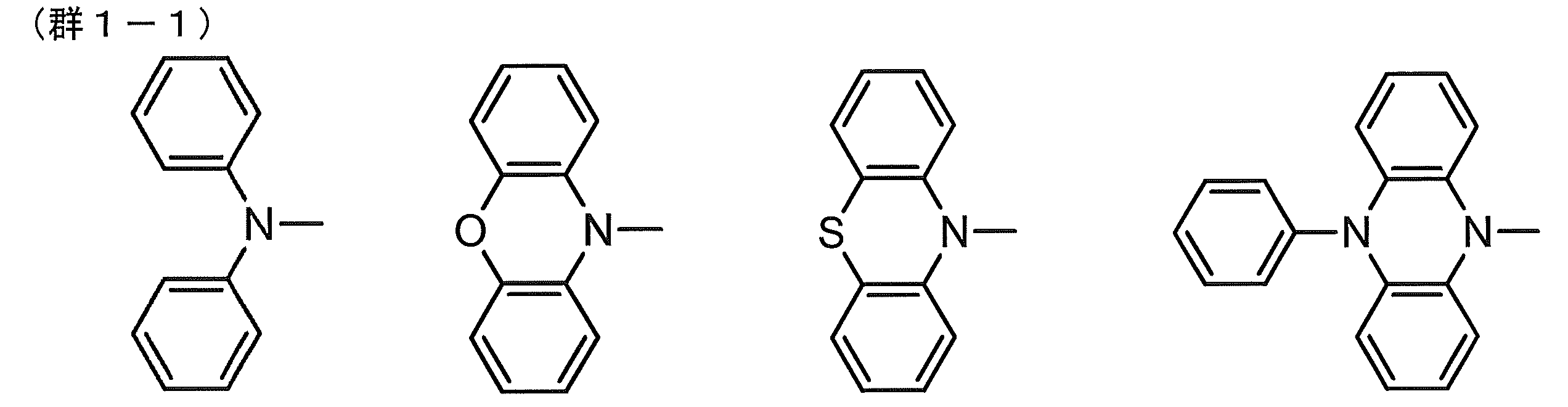
- D 1 , D 2 and D 3 each independently represents a hydrogen atom or a substituent, and at least one of D 1 , D 2 and D 3 is the following group 1-1:
- At least one of D 1 , D 2 and D 3 in the general formula (1) represents a diphenylamino group substituted at the meta position or the para position with a group having a structure selected from the group 1-1.
- At least one of D 1 , D 2 and D 3 in the general formula (1) is the following group 1-2:
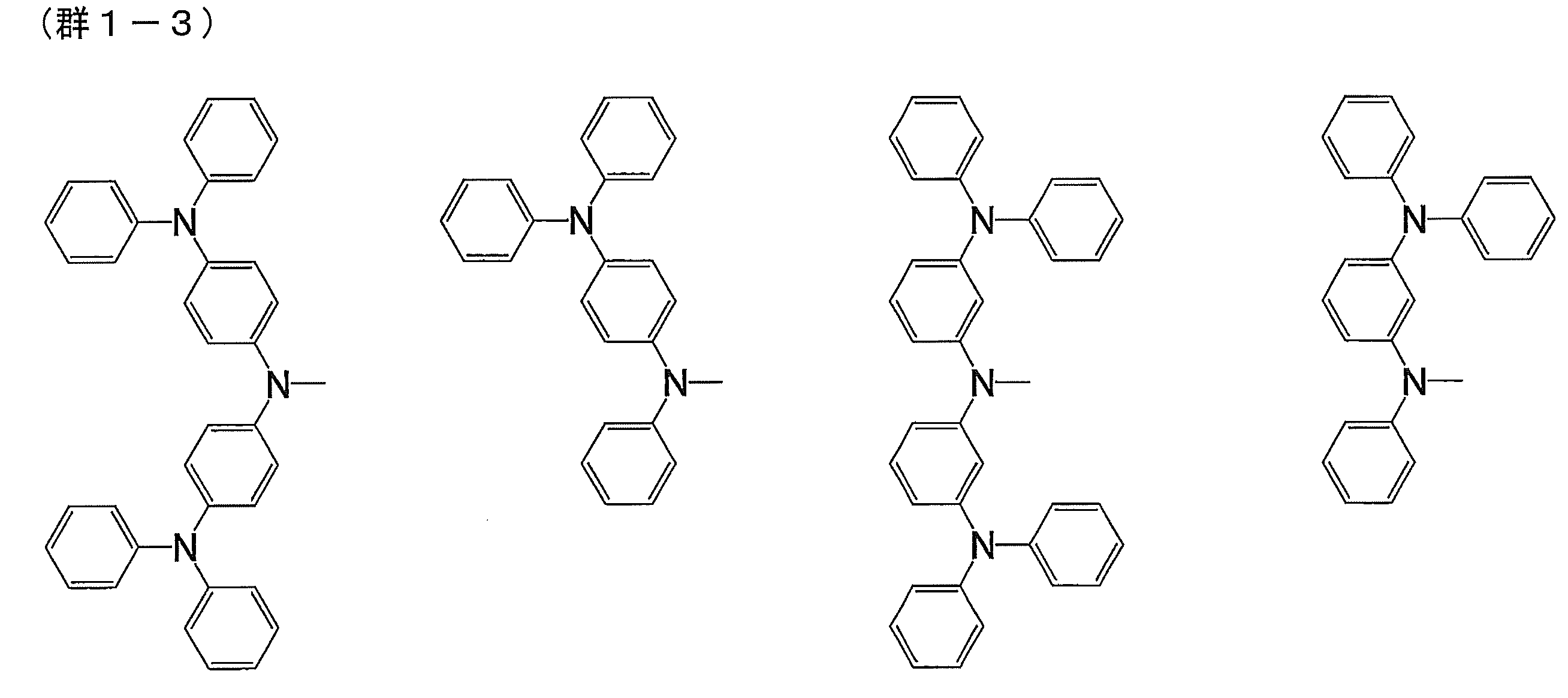
- At least one of D 1 , D 2 and D 3 in the general formula (1) is the following group 1-3:
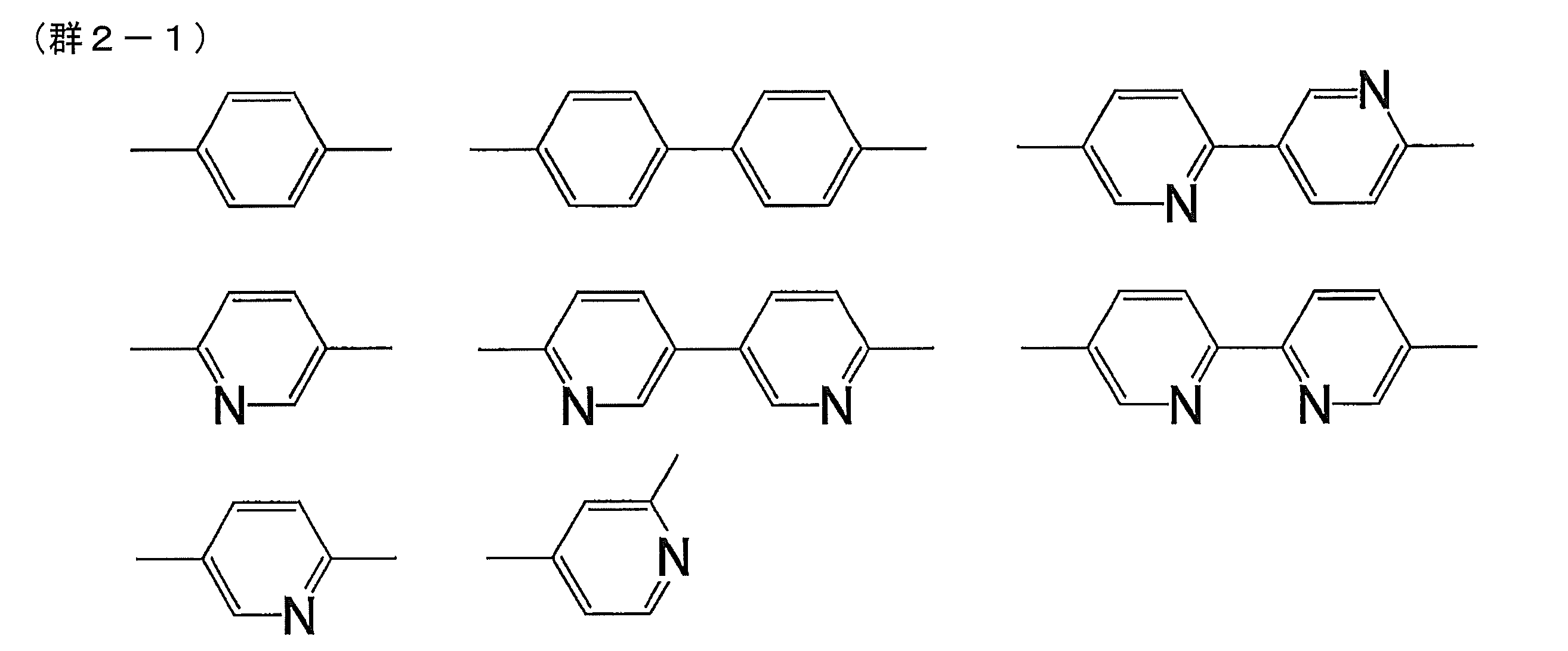
- Ar 1 , Ar 2 and Ar 3 in the general formula (1) are each independently a substituted or unsubstituted phenylene group, a substituted or unsubstituted pyridylene group, or a linking group in which any two of them are linked.
- the compound according to [5], which is a group selected from: [7] D 1 in the general formula (1) is a diarylamino group substituted with a group selected from the group 1-1, and Ar 1 is a substituted or unsubstituted paraphenylene group
- R 1 to R 12 and R 14 to R 25 each independently represents a hydrogen atom or a substituent.
- At least one of R 1 to R 10 is the following group 1-1: A diarylamino group substituted with a group selected from R 1 and R 2 , R 2 and R 3 , R 3 and R 4 , R 4 and R 5 , R 6 and R 7 , R 7 and R 8 , R 8 and R 9 , R 9 and R 10 , R 11 And R 12 , R 14 and R 15 , R 16 and R 17 , R 17 and R 18 , R 18 and R 19 , R 19 and R 20 , R 21 and R 22 , R 22 and R 23 , R 23 and R 24 , R 24 and R 25 may be bonded to each other to form a cyclic structure.
- At least one of R 1 to R 12 and R 14 to R 25 represents a diarylamino group substituted with a group selected from the group 1-1, and the other R 1 to R 12 and R 14 The compound according to [8], wherein -R 25 is a hydrogen atom.
- At least one of R 2 , R 3 , R 7 , R 8 represents a diarylamino group substituted with a group selected from the group 1-1 [8] or [8] 9].
- a light-emitting material comprising the compound according to any one of [1] to [10].
- a delayed phosphor comprising the compound according to any one of [1] to [10].
- An organic light emitting device comprising a light emitting layer containing the light emitting material according to [11] on a substrate.
- the organic light-emitting device according to [13] which emits delayed fluorescence.
- the compound of the present invention is useful as a light emitting material.
- the compounds of the present invention include those that emit delayed fluorescence.
- An organic light emitting device using the compound of the present invention as a light emitting material can realize high luminous efficiency.
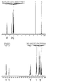
- FIG. 1 is a 1 H NMR spectrum of Compound 1.
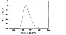
- 2 is an emission spectrum of the toluene solution of Example 1.
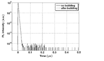
- 2 is a transient decay curve of the toluene solution of Example 1.
- FIG. 2 is an emission spectrum of a toluene solution of Comparative Example 1.
- 3 is a transient decay curve of the toluene solution of Comparative Example 1.
- 2 is an emission spectrum of the thin film type organic photoluminescence device of Example 2.
- 4 is a transient attenuation curve of the thin film type organic photoluminescence device of Example 2.
- 4 is an emission spectrum of the organic electroluminescence element of Example 3.
- 6 is a graph showing voltage-current density characteristics of the organic electroluminescence element of Example 3. 6 is a graph showing the current density-external quantum efficiency characteristics of the organic electroluminescence device of Example 3.
- a numerical range represented by using “to” means a range including numerical values described before and after “to” as a lower limit value and an upper limit value.
- the isotope species of the hydrogen atom present in the molecule of the compound used in the present invention is not particularly limited. For example, all the hydrogen atoms in the molecule may be 1 H, or a part or all of them are 2 H. (Deuterium D) may be used.
- D 1 , D 2 and D 3 each independently represent a hydrogen atom or a substituent.
- at least one of D 1 , D 2 and D 3 represents a diarylamino group substituted with a group selected from the following group 1-1.
- the hydrogen atom in each structure described in Group 1-1 may be substituted with a substituent.
- Each group in Group 1-1 is bonded to the aromatic ring of the diarylamino group at the nitrogen atom in the structure.
- the two aryl groups constituting the diarylamino group may be the same or different from each other. Preferred is the same case.
- the aryl group may be a single ring or a condensed ring, and preferably has 6 to 20 carbon atoms, more preferably 6 to 12 carbon atoms, and further preferably 6 to 10 carbon atoms. preferable.
- Examples of the diarylamino group include a diphenylamino group, a 1-naphthylphenylamino group, a di (1-naphthyl) amino group, a 2-naphthylphenylamino group, and a di (2-naphthyl) amino group. Is preferred.
- the group selected from Group 1-1 may be substituted at any position of the diarylamino group, but is preferably substituted at the meta or para position of the benzene ring bonded to the amino nitrogen. More preferably, it is substituted at the para position.
- diarylamino group only one diarylamino group may be substituted, or two or more groups may be substituted. When two or more are substituted, it is preferable that one or more of each benzene ring bonded to the amino nitrogen is substituted.
- the number of substituted groups selected from Group 1-1 is preferably 1 to 4, more preferably 1 or 2.
- Examples of the structure of the diarylamino group substituted with a group selected from Group 1-1 include the following Group 1-2.
- the hydrogen atom in each structure described in Group 1-2 may be substituted with a substituent.
- the diarylamino group substituted with a group selected from Group 1-1 is particularly preferably any group of the following Group 1-3.
- the hydrogen atom in each structure described in Group 1-3 may be substituted with a substituent.
- the hydrogen atom of the diarylamino group may be substituted with a substituent.
- the number of substituents is not particularly limited, and the substituents may not be present. When two or more substituents are present, these substituents may be the same as or different from each other.
- substituents examples include a hydroxy group, a halogen atom, a cyano group, an alkyl group having 1 to 20 carbon atoms, an alkoxy group having 1 to 20 carbon atoms, an alkylthio group having 1 to 20 carbon atoms, and an alkyl substitution having 1 to 20 carbon atoms.
- an amino group an acyl group having 2 to 20 carbon atoms, an aryl group having 6 to 40 carbon atoms, a heteroaryl group having 3 to 40 carbon atoms, a diarylamino group having 12 to 40 carbon atoms, a substituted or non-substituted group having 12 to 40 carbon atoms
- Substituted carbazolyl group alkenyl group having 2 to 10 carbon atoms, alkynyl group having 2 to 10 carbon atoms, alkoxycarbonyl group having 2 to 10 carbon atoms, alkylsulfonyl group having 1 to 10 carbon atoms, haloalkyl having 1 to 10 carbon atoms
- substituents are a halogen atom, a cyano group, a substituted or unsubstituted alkyl group having 1 to 20 carbon atoms, an alkoxy group having 1 to 20 carbon atoms, a substituted or unsubstituted aryl group having 6 to 40 carbon atoms, carbon A substituted or unsubstituted heteroaryl group having 3 to 40 carbon atoms, a substituted or unsubstituted diarylamino group having 12 to 40 carbon atoms, and a substituted or unsubstituted carbazolyl group having 12 to 40 carbon atoms.
- substituents are a fluorine atom, a chlorine atom, a cyano group, a substituted or unsubstituted alkyl group having 1 to 10 carbon atoms, a substituted or unsubstituted alkoxy group having 1 to 10 carbon atoms, and a substituted group having 1 to 10 carbon atoms.
- the alkyl group in the present specification may be linear, branched or cyclic, and more preferably has 1 to 6 carbon atoms. Specific examples thereof include a methyl group, an ethyl group, a propyl group, and butyl. A tert-butyl group, a pentyl group, a hexyl group and an isopropyl group.
- the aryl group may be a single ring or a fused ring, and specific examples thereof include a phenyl group and a naphthyl group.
- the alkoxy group may be linear, branched or cyclic, and more preferably has 1 to 6 carbon atoms.
- the two alkyl groups of the dialkylamino group may be the same or different from each other, but are preferably the same.
- the two alkyl groups of the dialkylamino group may each independently be linear, branched or cyclic, and more preferably have 1 to 6 carbon atoms.
- Specific examples include a methyl group, an ethyl group, Examples thereof include a propyl group, a butyl group, a pentyl group, a hexyl group, and an isopropyl group.
- the aryl group may be a single ring or a fused ring, and specific examples thereof include a phenyl group and a naphthyl group.
- the heteroaryl group may be a monocyclic ring or a fused ring, and specific examples include a pyridyl group, a pyridazyl group, a pyrimidyl group, a triazyl group, a triazolyl group, and a benzotriazolyl group.
- the diarylamino group substituted with a group selected from Group 1-1 may be at least one of D 1 , D 2 and D 3 , and any two or all three are Also good.
- the structures of the diarylamino groups substituted with a group selected from Group 1-1 may be the same or different.
- Ar 1 , Ar 2 and Ar 3 each independently represent a substituted or unsubstituted arylene group, a substituted or unsubstituted heteroarylene group, or a linking group in which any two of them are linked.
- a group in which an arylene group and a heteroarylene group are bonded to each other.
- the arylene group that Ar 1 , Ar 2, and Ar 3 can take may be a monocyclic arylene group or a condensed ring arylene group.
- Specific examples include 1,2-phenylene group, 1,3-phenylene group, 1,4-phenylene group, 1,2-naphthylene group, 1,3-naphthylene group, 1,4-naphthylene group, 1,5- Examples thereof include a naphthylene group and a 1,8-naphthylene group, and a 1,4-phenylene group and a 1,4-naphthylene group are preferable.
- the heteroarylene group that Ar 1 , Ar 2, and Ar 3 can take may be a monocyclic heteroarylene group or a condensed ring heteroarylene group.
- the heteroarylene group of the condensed ring includes a condensed ring of a benzene ring and a heterocyclic ring.
- Examples of the ring structure constituting the heteroarylene group include a pyridine ring, a pyridazine ring, a pyrimidine ring, a triazine ring, a triazole ring, and a benzotriazole ring, and a pyridine ring is preferable.
- Ar 1 , Ar 2, and Ar 3 are preferably each independently a substituted or unsubstituted phenylene group, a substituted or unsubstituted pyridylene group, or a linking group in which any two of these are linked, and each independently And more preferably a group selected from the group 2-1.
- the hydrogen atom in each structure described in Group 2-1 may be substituted with a substituent.
- D 1 in the general formula (1) represents a diarylamino group substituted with a group selected from Group 1-1
- Ar 1 is preferably a phenylene group, and preferably a 1,4-phenylene group. More preferred.
- D 2 in the general formula (1) represents a diarylamino group substituted with a group selected from Group 1-1
- Ar 2 is preferably a phenylene group, More preferably.
- D 3 in the general formula (1) represents a diarylamino group substituted with a group selected from Group 1-1
- Ar 3 is preferably a phenylene group, and is a 1,4-phenylene group It is more preferable.
- Ar 1 when D 1 in the general formula (1) is a hydrogen atom, Ar 2 when D 2 is a hydrogen atom, and Ar 3 when D 3 is a hydrogen atom are represented by the following groups 2-2: A selected group is preferred.
- the hydrogen atom in each structure described in Group 2-2 may be substituted with a substituent.
- the arylene group or heteroarylene group that Ar 1 , Ar 2, and Ar 3 can have may be substituted with a substituent, and a hydrogen atom in each structure described in the above groups 2-1 and 2-2 May be substituted with a substituent.
- the number of substituents is not particularly limited, and the substituents may not be present. When two or more substituents are present, these substituents may be the same as or different from each other. Examples of the substituent include a hydroxy group, a halogen atom, an alkyl group having 1 to 20 carbon atoms, an alkoxy group having 1 to 20 carbon atoms, an alkylthio group having 1 to 20 carbon atoms, an aryl group having 6 to 40 carbon atoms, and a carbon number.
- Examples thereof include 20 trialkylsilylalkyl groups, 5 to 20 trialkylsilylalkenyl groups, and 5 to 20 trialkylsilylalkynyl groups.
- those that can be substituted with a substituent may be further substituted.
- substituents are substituted or unsubstituted alkyl groups having 1 to 20 carbon atoms, alkoxy groups having 1 to 20 carbon atoms, substituted or unsubstituted aryl groups having 6 to 40 carbon atoms, and substituted groups having 3 to 40 carbon atoms. Or it is an unsubstituted heteroaryl group.
- Further preferred substituents are substituted or unsubstituted alkyl groups having 1 to 10 carbon atoms, substituted or unsubstituted alkoxy groups having 1 to 10 carbon atoms, substituted or unsubstituted aryl groups having 6 to 15 carbon atoms, 3 to 12 substituted or unsubstituted heteroaryl groups.
- D 1 is a diarylamino group substituted with a group selected from Group 1-1
- Ar 1 is a substituted or unsubstituted paraphenylene group.
- D 1 has a structure represented by the following general formula (2).
- R 1 to R 12 and R 14 to R 25 each independently represents a hydrogen atom or a substituent. At least one of R 1 to R 10 represents a diarylamino group substituted with a group selected from the above group 1-1.
- Descriptions and preferred ranges of substituents that can be taken by R 1 to R 12 are explanations and preferred ranges of substituents that can be taken by the structures described in the above groups 1-1, 1-2, and 1-3. Can be referred to.
- the explanation and preferred ranges of the substituents that can be taken by R 11 , R 12 , R 14 to R 25 are the explanations of the arylene groups and heteroarylene groups that Ar 1 , Ar 2, and Ar 3 can take. And a preferred range can be referred to.
- R 1 and R 2 , R 2 and R 3 , R 3 and R 4 , R 4 and R 5 , R 6 and R 7 , R 7 and R 8 , R 8 and R 9 , R 9 and R 10 , R 11 And R 12 , R 14 and R 15 , R 16 and R 17 , R 17 and R 18 , R 18 and R 19 , R 19 and R 20 , R 21 and R 22 , R 22 and R 23 , R 23 and R 24 , R 24 and R 25 may be bonded to each other to form a cyclic structure.
- the cyclic structure may be an aromatic ring or an alicyclic ring, may contain a hetero atom, and the cyclic structure may be a condensed ring of two or more rings.
- the hetero atom here is preferably selected from the group consisting of a nitrogen atom, an oxygen atom and a sulfur atom.
- cyclic structures formed include benzene ring, naphthalene ring, pyridine ring, pyridazine ring, pyrimidine ring, pyrazine ring, pyrrole ring, imidazole ring, pyrazole ring, triazole ring, imidazoline ring, oxazole ring, isoxazole ring, thiazole And a ring, an isothiazole ring, a cyclohexadiene ring, a cyclohexene ring, a cyclopentaene ring, a cycloheptatriene ring, a cycloheptadiene ring, and a cycloheptaene ring.
- a preferred group of compounds represented by the general formula (2) is a diarylamino group in which at least one of R 1 to R 12 and R 14 to R 25 is substituted with a group selected from the group 1-1.
- Other examples include compounds in which R 1 to R 12 and R 14 to R 25 are hydrogen atoms.
- at least one of R 2 , R 3 , R 7 and R 8 is substituted with a group selected from the group 1-1.
- a group of compounds that are diarylamino groups are diarylamino groups.
- the molecular weight of the compound represented by the general formula (1) is, for example, 1500 or less when the organic layer containing the compound represented by the general formula (1) is intended to be formed by vapor deposition. Preferably, it is preferably 1200 or less, more preferably 1000 or less, and even more preferably 800 or less.
- the lower limit of the molecular weight is the molecular weight of the minimum compound represented by the general formula (1).
- the compound represented by the general formula (1) may be formed by a coating method regardless of the molecular weight. If a coating method is used, a film can be formed even with a compound having a relatively large molecular weight.
- a compound containing a plurality of structures represented by the general formula (1) in the molecule as a light emitting material.
- a polymer obtained by previously polymerizing a polymerizable group in the structure represented by the general formula (1) and polymerizing the polymerizable group as a light emitting material Specifically, a monomer containing a polymerizable functional group is prepared in any one of Ar 1 , Ar 2 , Ar 3 , D 1 , D 2 , and D 3 in the general formula (1), and this is polymerized alone.
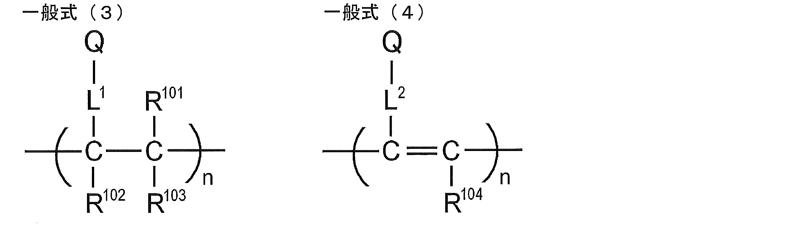
- polymer having a repeating unit including the structure represented by the general formula (1) a polymer including a structure represented by the following general formula (3) or (4) can be given.
- Q represents a group including the structure represented by the general formula (1)
- L 1 and L 2 represent a linking group.
- the linking group preferably has 0 to 20 carbon atoms, more preferably 1 to 15 carbon atoms, and still more preferably 2 to 10 carbon atoms. And preferably has a structure represented by - linking group -X 11 -L 11.
- X 11 represents an oxygen atom or a sulfur atom, and is preferably an oxygen atom.
- L 11 represents a linking group, preferably a substituted or unsubstituted alkylene group, or a substituted or unsubstituted arylene group, and a substituted or unsubstituted alkylene group having 1 to 10 carbon atoms, or a substituted or unsubstituted group A phenylene group is more preferable.
- R 101 , R 102 , R 103 and R 104 each independently represent a substituent.
- it is a substituted or unsubstituted alkyl group having 1 to 6 carbon atoms, a substituted or unsubstituted alkoxy group having 1 to 6 carbon atoms, or a halogen atom, more preferably an unsubstituted alkyl group having 1 to 3 carbon atoms.
- An unsubstituted alkoxy group having 1 to 3 carbon atoms, a fluorine atom, and a chlorine atom and more preferably an unsubstituted alkyl group having 1 to 3 carbon atoms and an unsubstituted alkoxy group having 1 to 3 carbon atoms.
- the linking group represented by L 1 and L 2 is any one of Ar 1 , Ar 2 , Ar 3 , D 1 , D 2 , and D 3 in the structure of the general formula (1) constituting Q, and the general formula (2 ) Can be bonded to any one of R 1 to R 12 and R 14 to R 25 .
- Two or more linking groups may be linked to one Q to form a crosslinked structure or a network structure.
- repeating unit examples include structures represented by the following formulas (5) to (8).
- a hydroxy group is introduced into either A or D of the structure of the general formula (1), and the following compound is used as a linker: It can be synthesized by reacting to introduce a polymerizable group and polymerizing the polymerizable group.
- the polymer containing a structure represented by the general formula (1) in the molecule may be a polymer consisting only of a repeating unit having the structure represented by the general formula (1), or other structures may be used. It may be a polymer containing repeating units.
- the repeating unit having a structure represented by the general formula (1) contained in the polymer may be a single type or two or more types. Examples of the repeating unit not having the structure represented by the general formula (1) include those derived from monomers used in ordinary copolymerization. Examples thereof include a repeating unit derived from a monomer having an ethylenically unsaturated bond such as ethylene and styrene.
- D 1 represents a diarylamino group substituted with a group selected from Group 1-1.
- X represents a halogen atom, and examples thereof include a fluorine atom, a chlorine atom, a bromine atom, and an iodine atom, and a chlorine atom, a bromine atom, and an iodine atom are preferable.
- the reaction in the above scheme is an application of a known coupling reaction, and known reaction conditions can be appropriately selected and used. The details of the above reaction can be referred to the synthesis examples described below.
- the compound represented by the general formula (1) can also be synthesized by combining other known synthesis reactions.
- the compound represented by the general formula (1) of the present invention is useful as a light emitting material of an organic light emitting device. For this reason, the compound represented by General formula (1) of this invention can be effectively used as a luminescent material for the light emitting layer of an organic light emitting element.
- the compound represented by the general formula (1) includes a delayed fluorescent material (delayed phosphor) that emits delayed fluorescence. That is, the present invention relates to a delayed phosphor having a structure represented by the general formula (1), an invention using a compound represented by the general formula (1) as a delayed phosphor, and a general formula (1).
- An invention of a method for emitting delayed fluorescence using the represented compound is also provided.
- An organic light emitting device using such a compound as a light emitting material emits delayed fluorescence and has a feature of high luminous efficiency. The principle will be described below by taking an organic electroluminescence element as an example.
- the organic electroluminescence element carriers are injected into the light emitting material from both positive and negative electrodes to generate an excited light emitting material and emit light.
- 25% of the generated excitons are excited to the excited singlet state, and the remaining 75% are excited to the excited triplet state. Therefore, the use efficiency of energy is higher when phosphorescence, which is light emission from an excited triplet state, is used.
- the excited triplet state has a long lifetime, energy saturation occurs due to saturation of the excited state and interaction with excitons in the excited triplet state, and in general, the quantum yield of phosphorescence is often not high.
- delayed fluorescent materials after energy transition to an excited triplet state due to intersystem crossing, etc., are then crossed back to an excited singlet state due to triplet-triplet annihilation or absorption of thermal energy, and emit fluorescence.
- a thermally activated delayed fluorescent material by absorption of thermal energy is particularly useful.
- excitons in the excited singlet state emit fluorescence as usual.
- excitons in the excited triplet state absorb heat generated by the device and cross between the excited singlets to emit fluorescence.
- the light is emitted from the excited singlet, the light is emitted at the same wavelength as the fluorescence, but the light lifetime (luminescence lifetime) generated by the reverse intersystem crossing from the excited triplet state to the excited singlet state is normal. Since the fluorescence becomes longer than the fluorescence and phosphorescence, it is observed as fluorescence delayed from these. This can be defined as delayed fluorescence. If such a heat-activated exciton transfer mechanism is used, the ratio of the compound in an excited singlet state, which normally generated only 25%, is increased to 25% or more by absorbing thermal energy after carrier injection. It can be raised.
- the heat of the device will sufficiently cause intersystem crossing from the excited triplet state to the excited singlet state and emit delayed fluorescence. Efficiency can be improved dramatically.
- the compound represented by the general formula (1) of the present invention as a light-emitting material of a light-emitting layer, excellent organic light-emitting devices such as an organic photoluminescence device (organic PL device) and an organic electroluminescence device (organic EL device) Can be provided.
- the compound represented by the general formula (1) of the present invention may have a function of assisting light emission of another light emitting material included in the light emitting layer as a so-called assist dopant. That is, the compound represented by the general formula (1) of the present invention contained in the light emitting layer includes the lowest excitation singlet energy level of the host material contained in the light emitting layer and the lowest excitation of other light emitting materials contained in the light emitting layer.
- the organic photoluminescence element has a structure in which at least a light emitting layer is formed on a substrate.
- the organic electroluminescence element has a structure in which an organic layer is formed at least between an anode, a cathode, and an anode and a cathode.
- the organic layer includes at least a light emitting layer, and may consist of only the light emitting layer, or may have one or more organic layers in addition to the light emitting layer. Examples of such other organic layers include a hole transport layer, a hole injection layer, an electron blocking layer, a hole blocking layer, an electron injection layer, an electron transport layer, and an exciton blocking layer.
- the hole transport layer may be a hole injection / transport layer having a hole injection function
- the electron transport layer may be an electron injection / transport layer having an electron injection function.
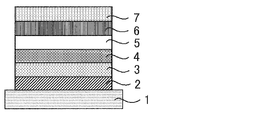
- FIG. 1 A specific example of the structure of an organic electroluminescence element is shown in FIG.
- 1 is a substrate
- 2 is an anode
- 3 is a hole injection layer
- 4 is a hole transport layer
- 5 is a light emitting layer
- 6 is an electron transport layer
- 7 is a cathode.
- each member and each layer of an organic electroluminescent element are demonstrated.
- substrate and a light emitting layer corresponds also to the board
- the organic electroluminescence device of the present invention is preferably supported on a substrate.
- the substrate is not particularly limited and may be any substrate conventionally used for organic electroluminescence elements.
- a substrate made of glass, transparent plastic, quartz, silicon, or the like can be used.
- an electrode material made of a metal, an alloy, an electrically conductive compound, or a mixture thereof having a high work function (4 eV or more) is preferably used.
- electrode materials include metals such as Au, and conductive transparent materials such as CuI, indium tin oxide (ITO), SnO 2 , and ZnO.
- conductive transparent materials such as CuI, indium tin oxide (ITO), SnO 2 , and ZnO.
- an amorphous material such as IDIXO (In 2 O 3 —ZnO) that can form a transparent conductive film may be used.
- a thin film may be formed by vapor deposition or sputtering of these electrode materials, and a pattern of a desired shape may be formed by photolithography, or when pattern accuracy is not so high (about 100 ⁇ m or more) ), A pattern may be formed through a mask having a desired shape at the time of vapor deposition or sputtering of the electrode material.
- wet film-forming methods such as a printing system and a coating system, can also be used.
- the transmittance be greater than 10%, and the sheet resistance as the anode is preferably several hundred ⁇ / ⁇ or less.
- the film thickness depends on the material, it is usually selected in the range of 10 to 1000 nm, preferably 10 to 200 nm.
- cathode a material having a low work function (4 eV or less) metal (referred to as an electron injecting metal), an alloy, an electrically conductive compound, and a mixture thereof as an electrode material is used.
- electrode materials include sodium, sodium-potassium alloy, magnesium, lithium, magnesium / copper mixture, magnesium / silver mixture, magnesium / aluminum mixture, magnesium / indium mixture, aluminum / aluminum oxide (Al 2 O 3 ) Mixtures, indium, lithium / aluminum mixtures, rare earth metals and the like.
- a mixture of an electron injecting metal and a second metal which is a stable metal having a larger work function value than this for example, a magnesium / silver mixture
- Suitable are a magnesium / aluminum mixture, a magnesium / indium mixture, an aluminum / aluminum oxide (Al 2 O 3 ) mixture, a lithium / aluminum mixture, aluminum and the like.
- the cathode can be produced by forming a thin film of these electrode materials by a method such as vapor deposition or sputtering.
- the sheet resistance as the cathode is preferably several hundred ⁇ / ⁇ or less, and the film thickness is usually selected in the range of 10 nm to 5 ⁇ m, preferably 50 to 200 nm.
- the emission luminance is advantageously improved.
- a transparent or semi-transparent cathode can be produced. By applying this, an element in which both the anode and the cathode are transparent is used. Can be produced.
- the light emitting layer is a layer that emits light after excitons are generated by recombination of holes and electrons injected from each of the anode and the cathode, and the light emitting material may be used alone for the light emitting layer. , Preferably including a luminescent material and a host material.
- a luminescent material the 1 type (s) or 2 or more types chosen from the compound group of this invention represented by General formula (1) can be used.
- a host material in addition to the light emitting material in the light emitting layer.
- the host material an organic compound having at least one of excited singlet energy and excited triplet energy higher than that of the light emitting material of the present invention can be used.
- singlet excitons and triplet excitons generated in the light emitting material of the present invention can be confined in the molecules of the light emitting material of the present invention, and the light emission efficiency can be sufficiently extracted.
- high luminous efficiency can be obtained, so that host materials that can achieve high luminous efficiency are particularly limited. And can be used in the present invention.
- the organic light emitting device or organic electroluminescent device of the present invention light emission is generated from the light emitting material of the present invention contained in the light emitting layer. This emission includes both fluorescence and delayed fluorescence. However, light emission from the host material may be partly or partly emitted.
- the amount of the compound of the present invention, which is a light emitting material is preferably 0.1% by weight or more, more preferably 1% by weight or more, and 50% or more. It is preferably no greater than wt%, more preferably no greater than 20 wt%, and even more preferably no greater than 10 wt%.
- the host material in the light-emitting layer is preferably an organic compound that has a hole transporting ability and an electron transporting ability, prevents the emission of longer wavelengths, and has a high glass transition temperature.
- the injection layer is a layer provided between the electrode and the organic layer for lowering the driving voltage and improving the luminance of light emission.
- the injection layer can be provided as necessary.
- the blocking layer is a layer that can prevent diffusion of charges (electrons or holes) and / or excitons existing in the light emitting layer to the outside of the light emitting layer.
- the electron blocking layer can be disposed between the light emitting layer and the hole transport layer and blocks electrons from passing through the light emitting layer toward the hole transport layer.
- a hole blocking layer can be disposed between the light emitting layer and the electron transporting layer to prevent holes from passing through the light emitting layer toward the electron transporting layer.
- the blocking layer can also be used to block excitons from diffusing outside the light emitting layer. That is, each of the electron blocking layer and the hole blocking layer can also function as an exciton blocking layer.
- the term “electron blocking layer” or “exciton blocking layer” as used herein is used in the sense of including a layer having the functions of an electron blocking layer and an exciton blocking layer in one layer.
- the hole blocking layer has a function of an electron transport layer in a broad sense.
- the hole blocking layer has a role of blocking holes from reaching the electron transport layer while transporting electrons, thereby improving the recombination probability of electrons and holes in the light emitting layer.
- the material for the hole blocking layer the material for the electron transport layer described later can be used as necessary.
- the electron blocking layer has a function of transporting holes in a broad sense.
- the electron blocking layer has a role to block electrons from reaching the hole transport layer while transporting holes, thereby improving the probability of recombination of electrons and holes in the light emitting layer. .
- the exciton blocking layer is a layer for preventing excitons generated by recombination of holes and electrons in the light emitting layer from diffusing into the charge transport layer. It becomes possible to efficiently confine in the light emitting layer, and the light emission efficiency of the device can be improved.
- the exciton blocking layer can be inserted on either the anode side or the cathode side adjacent to the light emitting layer, or both can be inserted simultaneously.
- the layer when the exciton blocking layer is provided on the anode side, the layer can be inserted adjacent to the light emitting layer between the hole transport layer and the light emitting layer, and when inserted on the cathode side, the light emitting layer and the cathode Between the luminescent layer and the light-emitting layer.
- a hole injection layer, an electron blocking layer, or the like can be provided between the anode and the exciton blocking layer adjacent to the anode side of the light emitting layer, and the excitation adjacent to the cathode and the cathode side of the light emitting layer can be provided.
- an electron injection layer, an electron transport layer, a hole blocking layer, and the like can be provided.
- the blocking layer is disposed, at least one of the excited singlet energy and the excited triplet energy of the material used as the blocking layer is preferably higher than the excited singlet energy and the excited triplet energy of the light emitting material.
- the hole transport layer is made of a hole transport material having a function of transporting holes, and the hole transport layer can be provided as a single layer or a plurality of layers.
- the hole transport material has any one of hole injection or transport and electron barrier properties, and may be either organic or inorganic.
- hole transport materials that can be used include, for example, triazole derivatives, oxadiazole derivatives, imidazole derivatives, carbazole derivatives, indolocarbazole derivatives, polyarylalkane derivatives, pyrazoline derivatives and pyrazolone derivatives, phenylenediamine derivatives, arylamine derivatives, Examples include amino-substituted chalcone derivatives, oxazole derivatives, styrylanthracene derivatives, fluorenone derivatives, hydrazone derivatives, stilbene derivatives, silazane derivatives, aniline copolymers, and conductive polymer oligomers, particularly thiophene oligomers.
- An aromatic tertiary amine compound and an styrylamine compound are preferably used, and an aromatic tertiary amine compound is more preferably used.
- the electron transport layer is made of a material having a function of transporting electrons, and the electron transport layer can be provided as a single layer or a plurality of layers.
- the electron transport material (which may also serve as a hole blocking material) may have a function of transmitting electrons injected from the cathode to the light emitting layer.
- Examples of the electron transport layer that can be used include nitro-substituted fluorene derivatives, diphenylquinone derivatives, thiopyran dioxide oxide derivatives, carbodiimides, fluorenylidenemethane derivatives, anthraquinodimethane and anthrone derivatives, oxadiazole derivatives, and the like.
- a thiadiazole derivative in which the oxygen atom of the oxadiazole ring is substituted with a sulfur atom, and a quinoxaline derivative having a quinoxaline ring known as an electron withdrawing group can also be used as an electron transport material.
- a polymer material in which these materials are introduced into a polymer chain or these materials are used as a polymer main chain can also be used.
- the compound represented by the general formula (1) may be used not only for the light emitting layer but also for layers other than the light emitting layer.
- the compound represented by General formula (1) used for a light emitting layer and the compound represented by General formula (1) used for layers other than a light emitting layer may be same or different.
- the compound represented by the general formula (1) may be used for the injection layer, blocking layer, hole blocking layer, electron blocking layer, exciton blocking layer, hole transporting layer, electron transporting layer, and the like. .
- the method for forming these layers is not particularly limited, and the layer may be formed by either a dry process or a wet process.
- the preferable material which can be used for an organic electroluminescent element is illustrated concretely.
- the material that can be used in the present invention is not limited to the following exemplary compounds. Moreover, even if it is a compound illustrated as a material which has a specific function, it can also be diverted as a material which has another function.
- R and R 2 to R 7 each independently represent a hydrogen atom or a substituent.
- n represents an integer of 3 to 5.
- the organic electroluminescence device produced by the above-described method emits light by applying an electric field between the anode and the cathode of the obtained device. At this time, if the light is emitted by excited singlet energy, light having a wavelength corresponding to the energy level is confirmed as fluorescence emission and delayed fluorescence emission. In addition, in the case of light emission by excited triplet energy, a wavelength corresponding to the energy level is confirmed as phosphorescence. Since normal fluorescence has a shorter fluorescence lifetime than delayed fluorescence, the emission lifetime can be distinguished from fluorescence and delayed fluorescence.
- the excited triplet energy is unstable and is converted into heat and the like, and the lifetime is short and it is immediately deactivated.
- the excited triplet energy of a normal organic compound it can be measured by observing light emission under extremely low temperature conditions.
- the organic electroluminescence element of the present invention can be applied to any of a single element, an element having a structure arranged in an array, and a structure in which an anode and a cathode are arranged in an XY matrix.
- an organic light emitting device with greatly improved light emission efficiency can be obtained by containing the compound represented by the general formula (1) in the light emitting layer.
- the organic light emitting device such as the organic electroluminescence device of the present invention can be further applied to various uses. For example, it is possible to produce an organic electroluminescence display device using the organic electroluminescence element of the present invention. For details, see “Organic EL Display” (Ohm Co., Ltd.) ) Can be referred to.
- the organic electroluminescence device of the present invention can be applied to organic electroluminescence illumination and backlights that are in great demand.
- FIG. 2 shows a 1 H-NMR spectrum (CDCl 3 , 500 MHz).
- 4,4′-dibromo-4 ′′-(4,6-diphenyl-1,3,5-triazin-2-yl) triphenylamine 1.50 g (2.36 mmol), diphenylamine 1.00 g (5.91 mmol) ), 43.2 mg (0.0472 mmol) of tris (dibenzylideneacetone) dipalladium (0) and 0.681 g (7.09 mmol) of sodium tert-butoxide were placed in a 100 mL three-necked flask, and the atmosphere in the flask was replaced with nitrogen.
- Example 1 Preparation and evaluation of organic photoluminescence device (solution)
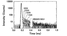
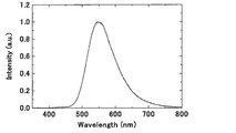
- a toluene solution of compound 1 synthesized in Synthesis Example 1 (concentration 10 ⁇ 5 mol / L) was prepared, and irradiated with ultraviolet light at 300 K while bubbling nitrogen. As shown in FIG. 3, the peak wavelength was 565 nm. Fluorescence was observed.
- an absolute PL quantum yield measurement device Quantaurus-QY manufactured by Hamamatsu Photonics Co., Ltd.
- FIG. 4 shows a transient decay curve after the nitrogen bubble.
- This transient decay curve shows the result of measuring the luminescence lifetime obtained by measuring the process in which the emission intensity is deactivated by applying excitation light to the compound.
- the light emission intensity decays in a single exponential manner. This means that if the vertical axis of the graph is semi-log, it will decay linearly.
- the transient decay curve of Compound 1 such a linear component (fluorescence) is observed at the beginning of observation, but after that, a component deviating from linearity appears. This is light emission of the delay component, and the signal added to the initial component becomes a loose curve with a tail on the long time side.
- Comparative Example 1 Preparation and Evaluation of Organic Photoluminescence Element (Solution) Instead of Compound 1, a toluene solution was prepared in the same manner as in Example 1 using Compound A as a comparative compound.
- FIG. 5 shows an emission spectrum
- FIG. 6 shows a transient decay curve. There was no difference between before and after the nitrogen bubble, and no delayed fluorescence was observed.
- Example 2 Preparation and evaluation of organic photoluminescence device (thin film)
- An emission spectrum obtained using the same measuring apparatus as in Example 1 is shown in FIG. 7 (peak wavelength 539 nm).
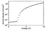
- Example 3 Production and Evaluation of Organic Electroluminescence Element
- ITO indium tin oxide
- Lamination was performed at 0 ⁇ 10 ⁇ 4 Pa.
- ⁇ -NPD was formed on ITO to a thickness of 35 nm.
- Compound 1 and mCBP were co-evaporated from different vapor deposition sources to form a layer having a thickness of 15 nm as a light emitting layer. At this time, the concentration of Compound 1 was 6.0% by weight.
- TPBi is formed to a thickness of 65 nm
- further lithium fluoride (LiF) is vacuum-deposited to 0.8 nm
- aluminum (Al) is evaporated to a thickness of 100 nm to form a cathode.
- a luminescence element was obtained.
- a semiconductor parameter analyzer manufactured by Agilent Technologies: E5273A
- an optical power meter measuring device manufactured by Newport: 1930C
- an optical spectrometer manufactured by Ocean Optics: USB2000
- the organic electroluminescence device using Compound 1 as the light emitting material achieved a high external quantum efficiency of 15.44%. Assuming that an ideal organic electroluminescence device balanced using a fluorescent material having a light emission quantum efficiency of 100% is prototyped, if the light extraction efficiency is 20 to 30%, the external quantum efficiency of fluorescence emission is 5%. 7.5%. This value is generally regarded as a theoretical limit value of the external quantum efficiency of an organic electroluminescence device using a fluorescent material. The organic electroluminescence device of the present invention using Compound 1 is extremely excellent in that high external quantum efficiency exceeding the theoretical limit value is realized.
- the compound of the present invention is useful as a luminescent material. For this reason, the compound of this invention is effectively used as a luminescent material for organic light emitting elements, such as an organic electroluminescent element. Since the compounds of the present invention include those that emit delayed fluorescence, it is also possible to provide an organic light-emitting device with high luminous efficiency. For this reason, this invention has high industrial applicability.
Abstract
下記一般式で表される化合物は発光材料として有用である。Ar1~Ar3はアリーレン基またはヘテロアリーレン基、D1~D3は水素原子または置換基を表し、D1~D3の少なくとも1つはジフェニルアミノ基等で置換されたジアリールアミノ基である。
Description
本発明は、発光材料として有用な化合物とそれを用いた有機発光素子に関する。
有機エレクトロルミネッセンス素子(有機EL素子)などの有機発光素子の発光効率を高める研究が盛んに行われている。特に、有機エレクトロルミネッセンス素子を構成する電子輸送材料、正孔輸送材料、発光材料などを新たに開発して組み合わせることにより、発光効率を高める工夫が種々なされてきている。その中には、トリアジン環とジフェニルアミノ基を含む化合物を利用した有機エレクトロルミネッセンス素子に関する研究も見受けられる。
例えば特許文献1には、有機エレクトロルミネッセンス素子を構成する一対の電極間に存在する発光層の中に、下記の一般式で表される化合物をホスト材料として用いることが記載されている。下記の一般式において、LC1は連結基を表し、ZC1は芳香族炭化水素環またはヘテロ環の形成に必要な原子群を表し、nC1は2以上の整数を表すものと規定されている。

特許文献1によると、LC1はさまざまな連結基をとりうることになっており、その中には2,4,6-トリアジントリイル基も含まれている。また、ZC1によって広範囲な環を形成しうることが記載されているが、ベンゼン環を形成する場合の置換基として、特定の基で置換されたジフェニルアミノ基を採用することについては言及がない。特許文献1には、LC1が2,4,6-トリアジントリイル基であって、ZC1によってベンゼン環を形成しており、そのベンゼン環にジフェニルアミノ基が置換されている化合物として、下記の2つの構造が具体的に記載されている。そのうち、化合物Aについては実施例にてホスト材料としての有用性が確認されている。

このように、特許文献1にはトリアジン環とジフェニルアミノ基を含む化合物を有機エレクトロルミネッセンス素子の発光層のホスト材料として用いることが記載されている。しかしながら、特許文献1に記載される化合物が、発光材料として機能しうるものであるか否かについては一切記載されていない。発光材料とホスト材料は機能が異なることから、特許文献1に記載される化合物の発光材料としての有用性は不明である。本願発明者らが検討したところでは、特許文献1に記載されている化合物の発光特性に際立った特徴は見出されなかった。
このような状況下において本発明者らは、トリアジン環とジフェニルアミノ基を含んでいるが特許文献1には記載されていない構造について検討を始め、発光特性が優れた化合物を見出すことを目指して研究を重ねた。そして、発光材料として有用な化合物の一般式を導きだし、発光効率が高い有機発光素子の構成を一般化することを目的として鋭意検討を進めた。
鋭意検討を進めた結果、本発明者らは、特定の構造を有する化合物群を合成することに成功するとともに、それらの化合物群が発光材料として優れた性質を有することを見出した。また、そのような化合物群の中に、遅延蛍光材料として有用なものがあることを見出し、発光効率が高い有機発光素子を安価に提供しうることを明らかにした。本発明者らは、これらの知見に基づいて、上記の課題を解決する手段として、以下の本発明を提供するに至った。
[1] 下記一般式(1)で表される化合物。
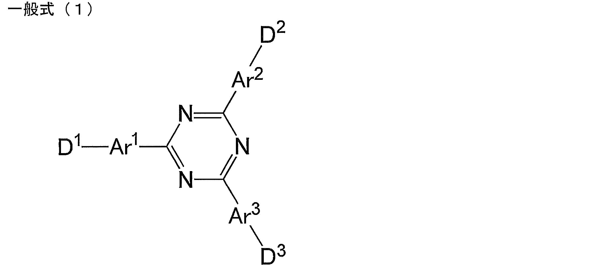
[一般式(1)において、Ar1、Ar2およびAr3は各々独立に置換もしくは無置換のアリーレン基、置換もしくは無置換のヘテロアリーレン基、またはこれらのいずれか2つが連結した連結基を表す。D1、D2およびD3は各々独立に水素原子または置換基を表し、D1、D2およびD3の少なくとも1つは下記の群1-1:

から選択される基で置換されたジアリールアミノ基を表す。]
[2] 一般式(1)のD1、D2およびD3の少なくとも1つが、前記群1-1から選択される構造を有する基でメタ位またはパラ位が置換されたジフェニルアミノ基を表すことを特徴とする[1]に記載の化合物。
[2] 一般式(1)のD1、D2およびD3の少なくとも1つが、前記群1-1から選択される構造を有する基でメタ位またはパラ位が置換されたジフェニルアミノ基を表すことを特徴とする[1]に記載の化合物。
[3] 一般式(1)のD1、D2およびD3の少なくとも1つが、下記の群1-2:


から選択される基で置換されたジアリールアミノ基であることを特徴とする[2]に記載の化合物。
[4] 一般式(1)のD1、D2およびD3の少なくとも1つが、下記の群1-3:

から選択される基で置換されたジアリールアミノ基であることを特徴とする[3]に記載の化合物。
[4] 一般式(1)のD1、D2およびD3の少なくとも1つが、下記の群1-3:
[5] 一般式(1)のAr1、Ar2およびAr3が、各々独立に置換もしくは無置換のフェニレン基、置換もしくは無置換のピリジレン基、またはこれらのいずれか2つが連結した連結基であることを特徴とする[1]~[4]のいずれか1項に記載の化合物。
[6] 一般式(1)のAr1、Ar2およびAr3が、各々独立に下記の群2-1:

から選択される基であることを特徴とする[5]に記載の化合物。
[7] 一般式(1)のD1が前記の群1-1から選択される基で置換されたジアリールアミノ基であって、Ar1が置換もしくは無置換のパラフェニレン基であることを特徴とする[1]~[6]のいずれか1項に記載の化合物。
[6] 一般式(1)のAr1、Ar2およびAr3が、各々独立に下記の群2-1:
[7] 一般式(1)のD1が前記の群1-1から選択される基で置換されたジアリールアミノ基であって、Ar1が置換もしくは無置換のパラフェニレン基であることを特徴とする[1]~[6]のいずれか1項に記載の化合物。
[8] 下記一般式(2)で表される構造を有する[1]に記載の化合物。

[一般式(2)において、R1~R12およびR14~R25は各々独立に水素原子または置換基を表す。R1~R10のうちの少なくとも1つは下記の群1-1:

から選択される基で置換されたジアリールアミノ基を表す。R1とR2、R2とR3、R3とR4、R4とR5、R6とR7、R7とR8、R8とR9、R9とR10、R11とR12、R14とR15、R16とR17、R17とR18、R18とR19、R19とR20、R21とR22、R22とR23、R23とR24、R24とR25は、各々互いに結合して環状構造を形成していてもよい。]
[9] R1~R12およびR14~R25のうちの少なくとも1つが前記群1-1から選択される基で置換されたジアリールアミノ基を表し、その他のR1~R12およびR14~R25が水素原子であることを特徴とする[8]に記載の化合物。
[10] R2、R3、R7、R8のうちの少なくとも1つが、前記群1-1から選択される基で置換されたジアリールアミノ基を表すことを特徴とする[8]または[9]に記載の化合物。
[9] R1~R12およびR14~R25のうちの少なくとも1つが前記群1-1から選択される基で置換されたジアリールアミノ基を表し、その他のR1~R12およびR14~R25が水素原子であることを特徴とする[8]に記載の化合物。
[10] R2、R3、R7、R8のうちの少なくとも1つが、前記群1-1から選択される基で置換されたジアリールアミノ基を表すことを特徴とする[8]または[9]に記載の化合物。
[11] [1]~[10]のいずれか1項に記載の化合物からなる発光材料。
[12] [1]~[10]のいずれか1項に記載の化合物からなる遅延蛍光体。
[13] [11]に記載の発光材料を含む発光層を基板上に有することを特徴とする有機発光素子。
[14] 遅延蛍光を放射することを特徴とする[13]に記載の有機発光素子。
[15] 有機エレクトロルミネッセンス素子であることを特徴とする[13]または[14]に記載の有機発光素子。
[12] [1]~[10]のいずれか1項に記載の化合物からなる遅延蛍光体。
[13] [11]に記載の発光材料を含む発光層を基板上に有することを特徴とする有機発光素子。
[14] 遅延蛍光を放射することを特徴とする[13]に記載の有機発光素子。
[15] 有機エレクトロルミネッセンス素子であることを特徴とする[13]または[14]に記載の有機発光素子。
本発明の化合物は、発光材料として有用である。また、本発明の化合物の中には遅延蛍光を放射するものが含まれている。本発明の化合物を発光材料として用いた有機発光素子は、高い発光効率を実現しうる。
以下において、本発明の内容について詳細に説明する。以下に記載する構成要件の説明は、本発明の代表的な実施態様や具体例に基づいてなされることがあるが、本発明はそのような実施態様や具体例に限定されるものではない。なお、本明細書において「~」を用いて表される数値範囲は、「~」の前後に記載される数値を下限値および上限値として含む範囲を意味する。また、本発明に用いられる化合物の分子内に存在する水素原子の同位体種は特に限定されず、例えば分子内の水素原子がすべて1Hであってもよいし、一部または全部が2H(デューテリウムD)であってもよい。
[一般式(1)で表される化合物]
本発明の化合物は、下記一般式(1)で表される構造を有することを特徴とする。

本発明の化合物は、下記一般式(1)で表される構造を有することを特徴とする。
一般式(1)におけるD1、D2およびD3は、各々独立に水素原子または置換基を表す。ここで、D1、D2およびD3の少なくとも1つは、下記の群1-1から選択される基で置換されたジアリールアミノ基を表す。群1-1に記載される各構造中の水素原子は置換基で置換されていてもよい。群1-1の各基は、その構造中の窒素原子でジアリールアミノ基の芳香環に結合する。
上記のジアリールアミノ基を構成する2つのアリール基は、同一であってもよいし、互いに異なっていてもよい。好ましいのは同一である場合である。アリール基は、単環であっても縮合環であってもよく、環構成炭素数は6~20であることが好ましく、6~12であることがより好ましく、6~10であることがさらに好ましい。ジアリールアミノ基としては、ジフェニルアミノ基、1-ナフチルフェニルアミノ基、ジ(1-ナフチル)アミノ基、2-ナフチルフェニルアミノ基、ジ(2-ナフチル)アミノ基を挙げることができ、ジフェニルアミノ基が好ましい。
群1-1から選択される基は、ジアリールアミノ基のいずれの位置に置換されていてもよいが、アミノ窒素に結合しているベンゼン環のメタ位またはパラ位に置換されていることが好ましく、パラ位に置換されていることがより好ましい。
群1-1から選択される基は、ジアリールアミノ基のいずれの位置に置換されていてもよいが、アミノ窒素に結合しているベンゼン環のメタ位またはパラ位に置換されていることが好ましく、パラ位に置換されていることがより好ましい。
群1-1から選択される基は、ジアリールアミノ基に1つだけ置換されていてもよいし、2つ以上置換されていてもよい。2つ以上置換されている場合は、アミノ窒素に結合している各ベンゼン環にそれぞれ1つ以上ずつ置換されていることが好ましい。群1-1から選択される基の置換個数は1~4であることが好ましく、1または2であることがより好ましい。
群1-1から選択される基で置換されたジアリールアミノ基の構造例として、下記の群1-2を挙げることができる。群1-2に記載される各構造中の水素原子は置換基で置換されていてもよい。


群1-1から選択される基で置換されたジアリールアミノ基は、特に下記の群1-3のいずれかの基であることが好ましい。群1-3に記載される各構造中の水素原子は置換基で置換されていてもよい。
上記の群1-1、群1-2、群1-3に記載される各構造中の水素原子や、群1-1、群1-2、群1-3に記載される基で置換されるジアリールアミノ基の水素原子は、置換基で置換されていてもよい。置換基の数は特に制限されず、置換基は存在していなくてもよい。また、2つ以上の置換基が存在するときは、それらの置換基は互いに同一であっても異なっていてもよい。置換基としては、例えばヒドロキシ基、ハロゲン原子、シアノ基、炭素数1~20のアルキル基、炭素数1~20のアルコキシ基、炭素数1~20のアルキルチオ基、炭素数1~20のアルキル置換アミノ基、炭素数2~20のアシル基、炭素数6~40のアリール基、炭素数3~40のヘテロアリール基、炭素数12~40のジアリールアミノ基、炭素数12~40の置換もしくは無置換のカルバゾリル基、炭素数2~10のアルケニル基、炭素数2~10のアルキニル基、炭素数2~10のアルコキシカルボニル基、炭素数1~10のアルキルスルホニル基、炭素数1~10のハロアルキル基、アミド基、炭素数2~10のアルキルアミド基、炭素数3~20のトリアルキルシリル基、炭素数4~20のトリアルキルシリルアルキル基、炭素数5~20のトリアルキルシリルアルケニル基、炭素数5~20のトリアルキルシリルアルキニル基およびニトロ基等が挙げられる。これらの具体例のうち、さらに置換基により置換可能なものは置換されていてもよい。より好ましい置換基は、ハロゲン原子、シアノ基、炭素数1~20の置換もしくは無置換のアルキル基、炭素数1~20のアルコキシ基、炭素数6~40の置換もしくは無置換のアリール基、炭素数3~40の置換もしくは無置換のヘテロアリール基、炭素数12~40の置換もしくは無置換のジアリールアミノ基、炭素数12~40の置換もしくは無置換のカルバゾリル基である。さらに好ましい置換基は、フッ素原子、塩素原子、シアノ基、炭素数1~10の置換もしくは無置換のアルキル基、炭素数1~10の置換もしくは無置換のアルコキシ基、炭素数1~10の置換もしくは無置換のジアルキルアミノ基、炭素数6~15の置換もしくは無置換のアリール基、炭素数3~12の置換もしくは無置換のヘテロアリール基である。
本明細書でいうアルキル基は、直鎖状、分枝状、環状のいずれであってもよく、より好ましくは炭素数1~6であり、具体例としてメチル基、エチル基、プロピル基、ブチル基、tert-ブチル基、ペンチル基、ヘキシル基、イソプロピル基を挙げることができる。アリール基は、単環でも融合環でもよく、具体例としてフェニル基、ナフチル基を挙げることができる。アルコキシ基は、直鎖状、分枝状、環状のいずれであってもよく、より好ましくは炭素数1~6であり、具体例としてメトキシ基、エトキシ基、プロポキシ基、ブトキシ基、tert-ブトキシ基、ペンチルオキシ基、ヘキシルオキシ基、イソプロピポキシ基を挙げることができる。ジアルキルアミノ基の2つのアルキル基は、互いに同一であっても異なっていてもよいが、同一であることが好ましい。ジアルキルアミノ基の2つのアルキル基は、各々独立に直鎖状、分枝状、環状のいずれであってもよく、より好ましくは炭素数1~6であり、具体例としてメチル基、エチル基、プロピル基、ブチル基、ペンチル基、ヘキシル基、イソプロピル基を挙げることができる。アリール基は、単環でも融合環でもよく、具体例としてフェニル基、ナフチル基を挙げることができる。ヘテロアリール基も、単環でも融合環でもよく、具体例としてピリジル基、ピリダジル基、ピリミジル基、トリアジル基、トリアゾリル基、ベンゾトリアゾリル基を挙げることができる。
群1-1から選択される基で置換されたジアリールアミノ基は、D1、D2およびD3の少なくとも1つであればよく、いずれか2つであっても、3つすべてであってもよい。2つ以上である場合は、群1-1から選択される基で置換されたジアリールアミノ基の構造は、互いに同一であっても異なっていてもよい。D1、D2およびD3のすべてが群1-1から選択される基で置換されたジアリールアミノ基である場合は、D1-Ar1-で表される基、D2-Ar2-で表される基、D3-Ar3-で表される基のすべてが同一である化合物も好ましい。
一般式(1)において、Ar1、Ar2およびAr3は各々独立に置換もしくは無置換のアリーレン基、置換もしくは無置換のヘテロアリーレン基、またはこれらのいずれか2つが連結した連結基を表す。2つが連結した連結基には、2つの同じアリーレン基が結合した基、2つの互いに異なるアリーレン基が結合した基、2つの同じヘテロアリーレン基が結合した基、2つの互いに異なるヘテロアリーレン基が結合した基、アリーレン基とヘテロアリーレン基が結合した基が含まれる。
Ar1、Ar2およびAr3がとりうるアリーレン基は、単環のアリーレン基であっても、縮合環のアリーレン基であってもよい。具体例として、1,2-フェニレン基、1,3-フェニレン基、1,4-フェニレン基、1,2-ナフチレン基、1,3-ナフチレン基、1,4-ナフチレン基、1,5-ナフチレン基、1,8-ナフチレン基を挙げることができ、1,4-フェニレン基、1,4-ナフチレン基が好ましい。Ar1、Ar2およびAr3がとりうるヘテロアリーレン基も、単環のヘテロアリーレン基であっても、縮合環のヘテロアリーレン基であってもよい。縮合環のヘテロアリーレン基にはベンゼン環とヘテロ環の縮合環も含まれる。ヘテロアリーレン基を構成する環構造の例として、ピリジン環、ピリダジン環、ピリミジン環、トリアジン環、トリアゾール環、ベンゾトリアゾール環を挙げることができ、ピリジン環が好ましい。
Ar1、Ar2およびAr3は、各々独立に置換もしくは無置換のフェニレン基、置換もしくは無置換のピリジレン基、またはこれらのいずれか2つが連結した連結基であることが好ましく、各々独立に下記の群2-1から選択される基であることがより好ましい。群2-1に記載される各構造中の水素原子は置換基で置換されていてもよい。
一般式(1)のD1が群1-1から選択される基で置換されたジアリールアミノ基を表すとき、Ar1はフェニレン基であることが好ましく、1,4-フェニレン基であることがより好ましい。同様に、一般式(1)のD2が群1-1から選択される基で置換されたジアリールアミノ基を表すとき、Ar2はフェニレン基であることが好ましく、1,4-フェニレン基であることがより好ましい。また、一般式(1)のD3が群1-1から選択される基で置換されたジアリールアミノ基を表すとき、Ar3はフェニレン基であることが好ましく、1,4-フェニレン基であることがより好ましい。
一般式(1)のD1が水素原子であるときのAr1、D2が水素原子であるときのAr2、D3が水素原子であるときのAr3は、下記の群2-2から選択される基であることが好ましい。群2-2に記載される各構造中の水素原子は置換基で置換されていてもよい。

Ar1、Ar2およびAr3がとりうるアリーレン基やヘテロアリーレン基は置換基で置換されていてもよく、また上記の群2-1、群2-2に記載される各構造中の水素原子も置換基で置換されていてもよい。置換基の数は特に制限されず、置換基は存在していなくてもよい。また、2つ以上の置換基が存在するときは、それらの置換基は互いに同一であっても異なっていてもよい。置換基としては、例えばヒドロキシ基、ハロゲン原子、炭素数1~20のアルキル基、炭素数1~20のアルコキシ基、炭素数1~20のアルキルチオ基、炭素数6~40のアリール基、炭素数3~40のヘテロアリール基、炭素数2~10のアルケニル基、炭素数2~10のアルキニル基、炭素数1~10のハロアルキル基、炭素数3~20のトリアルキルシリル基、炭素数4~20のトリアルキルシリルアルキル基、炭素数5~20のトリアルキルシリルアルケニル基、炭素数5~20のトリアルキルシリルアルキニル基等が挙げられる。これらの具体例のうち、さらに置換基により置換可能なものは置換されていてもよい。より好ましい置換基は、炭素数1~20の置換もしくは無置換のアルキル基、炭素数1~20のアルコキシ基、炭素数6~40の置換もしくは無置換のアリール基、炭素数3~40の置換もしくは無置換のヘテロアリール基である。さらに好ましい置換基は、炭素数1~10の置換もしくは無置換のアルキル基、炭素数1~10の置換もしくは無置換のアルコキシ基、炭素数6~15の置換もしくは無置換のアリール基、炭素数3~12の置換もしくは無置換のヘテロアリール基である。
一般式(1)で表される化合物は、D1が群1-1から選択される基で置換されたジアリールアミノ基であって、Ar1が置換もしくは無置換のパラフェニレン基であることが好ましく、下記の一般式(2)で表される構造を有するものであることがより好ましい。

一般式(2)において、R1~R12およびR14~R25は各々独立に水素原子または置換基を表す。R1~R10のうちの少なくとも1つは上記の群1-1から選択される基で置換されたジアリールアミノ基を表す。
R1~R12がとりうる置換基の説明と好ましい範囲については、上記の群1-1、群1-2、群1-3に記載される各構造がとりうる置換基の説明と好ましい範囲を参照することができる。また、R11、R12、R14~R25がとりうる置換基の説明と好ましい範囲については、上記のAr1、Ar2およびAr3がとりうるアリーレン基やヘテロアリーレン基の置換基の説明と好ましい範囲を参照することができる。
R1~R12がとりうる置換基の説明と好ましい範囲については、上記の群1-1、群1-2、群1-3に記載される各構造がとりうる置換基の説明と好ましい範囲を参照することができる。また、R11、R12、R14~R25がとりうる置換基の説明と好ましい範囲については、上記のAr1、Ar2およびAr3がとりうるアリーレン基やヘテロアリーレン基の置換基の説明と好ましい範囲を参照することができる。
R1とR2、R2とR3、R3とR4、R4とR5、R6とR7、R7とR8、R8とR9、R9とR10、R11とR12、R14とR15、R16とR17、R17とR18、R18とR19、R19とR20、R21とR22、R22とR23、R23とR24、R24とR25は、各々互いに結合して環状構造を形成していてもよい。環状構造は芳香環であっても脂肪環であってもよく、またヘテロ原子を含むものであってもよく、さらに環状構造は2環以上の縮合環であってもよい。ここでいうヘテロ原子としては、窒素原子、酸素原子および硫黄原子からなる群より選択されるものであることが好ましい。形成される環状構造の例として、ベンゼン環、ナフタレン環、ピリジン環、ピリダジン環、ピリミジン環、ピラジン環、ピロール環、イミダゾール環、ピラゾール環、トリアゾール環、イミダゾリン環、オキサゾール環、イソオキサゾール環、チアゾール環、イソチアゾール環、シクロヘキサジエン環、シクロヘキセン環、シクロペンタエン環、シクロヘプタトリエン環、シクロヘプタジエン環、シクロヘプタエン環などを挙げることができる。
一般式(2)で表される化合物の好ましい一群として、R1~R12およびR14~R25のうちの少なくとも1つが前記群1-1から選択される基で置換されたジアリールアミノ基であり、その他のR1~R12およびR14~R25が水素原子である化合物群を挙げることができる。
また、一般式(2)で表される化合物の別の好ましい一群として、R2、R3、R7、R8のうちの少なくとも1つが、前記群1-1から選択される基で置換されたジアリールアミノ基である化合物群を挙げることができる。
また、一般式(2)で表される化合物の別の好ましい一群として、R2、R3、R7、R8のうちの少なくとも1つが、前記群1-1から選択される基で置換されたジアリールアミノ基である化合物群を挙げることができる。
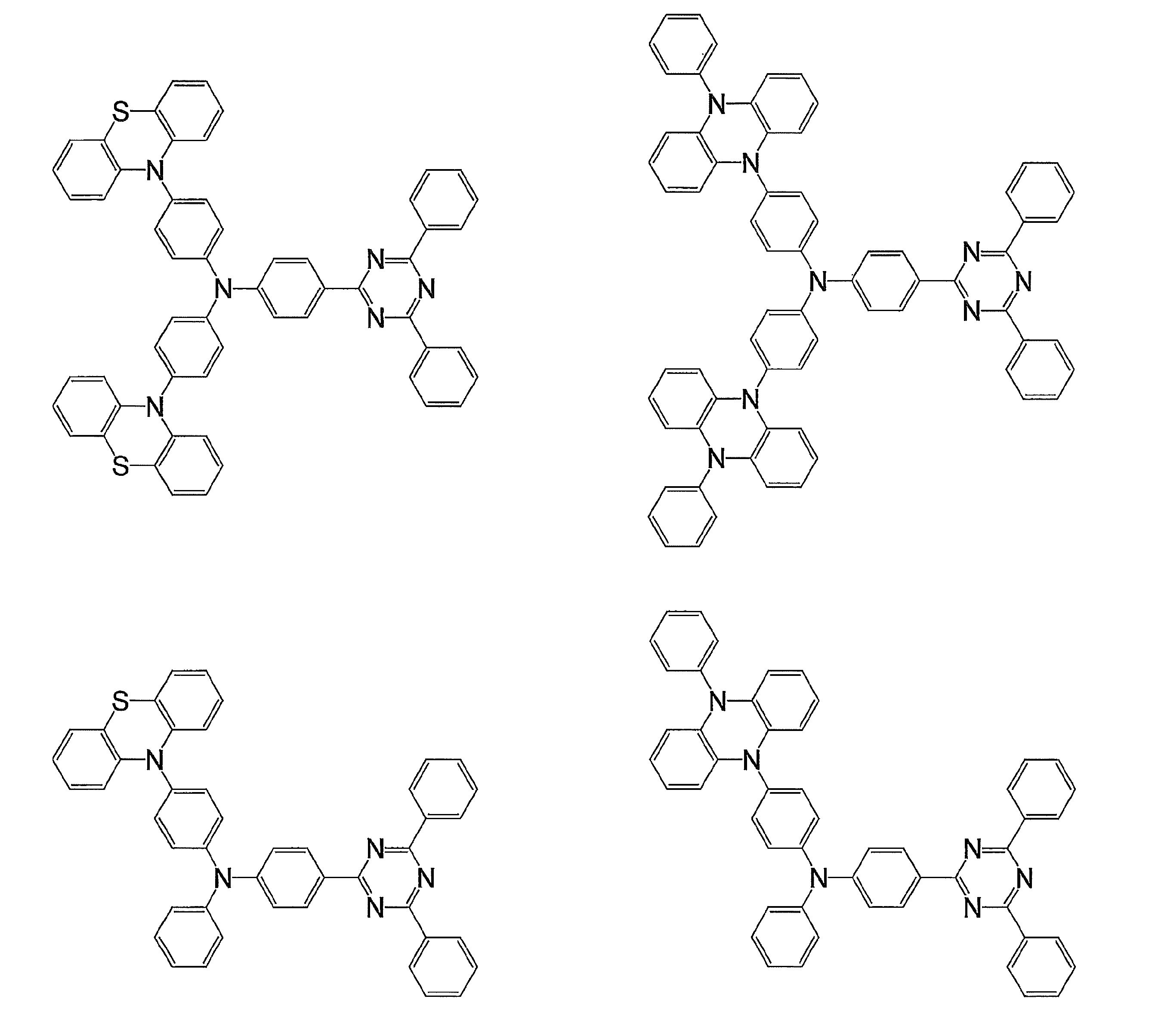
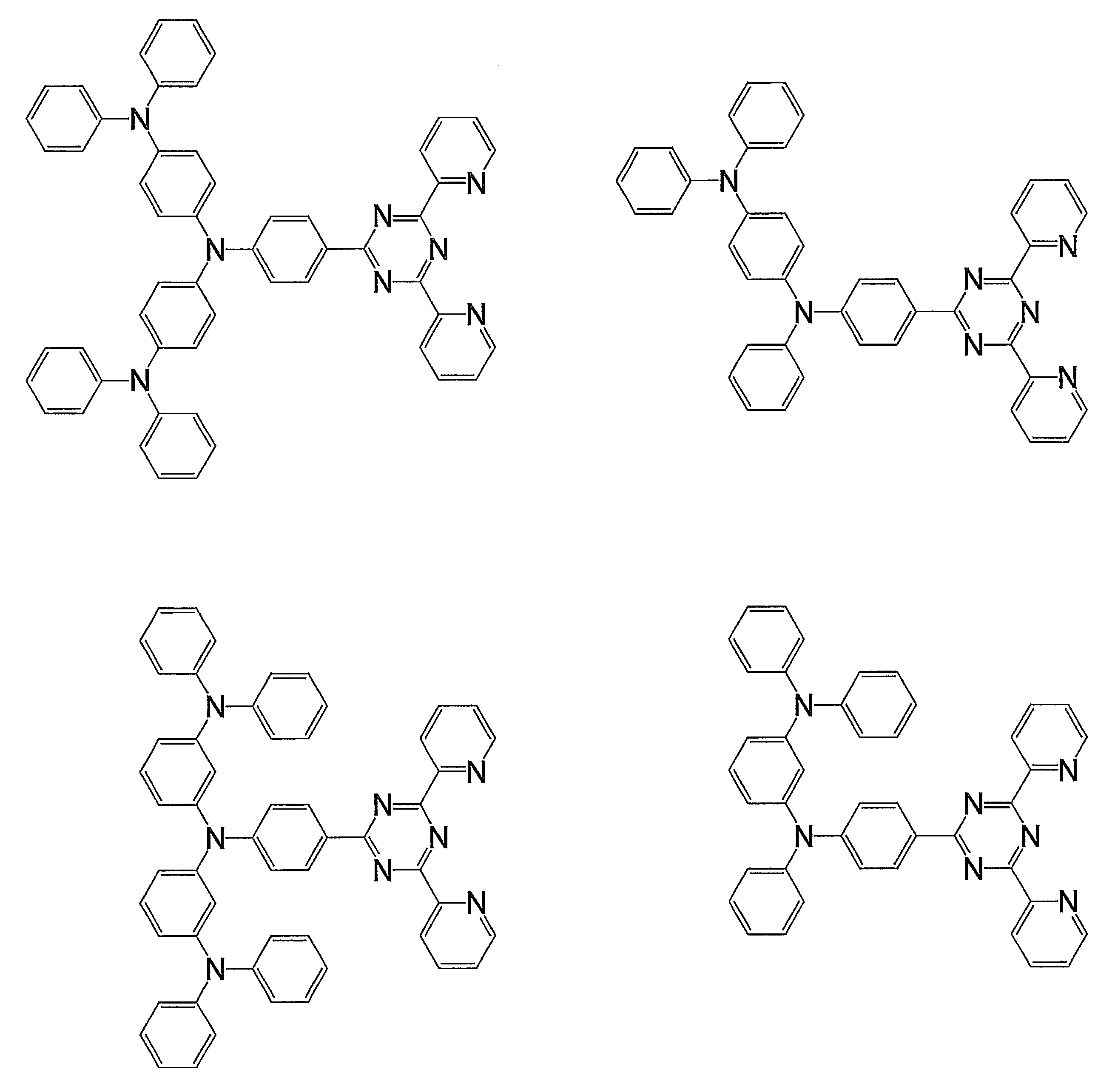
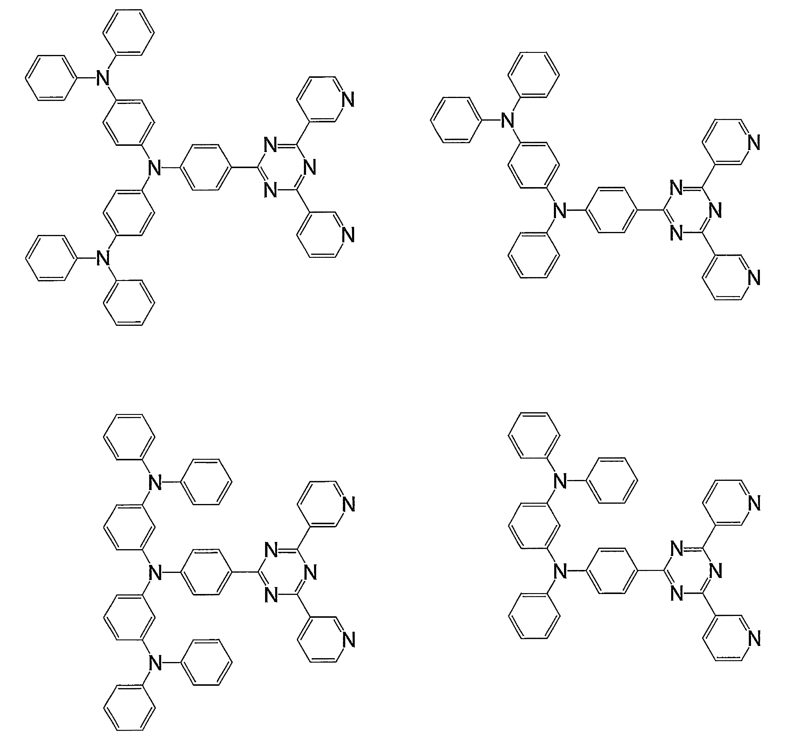
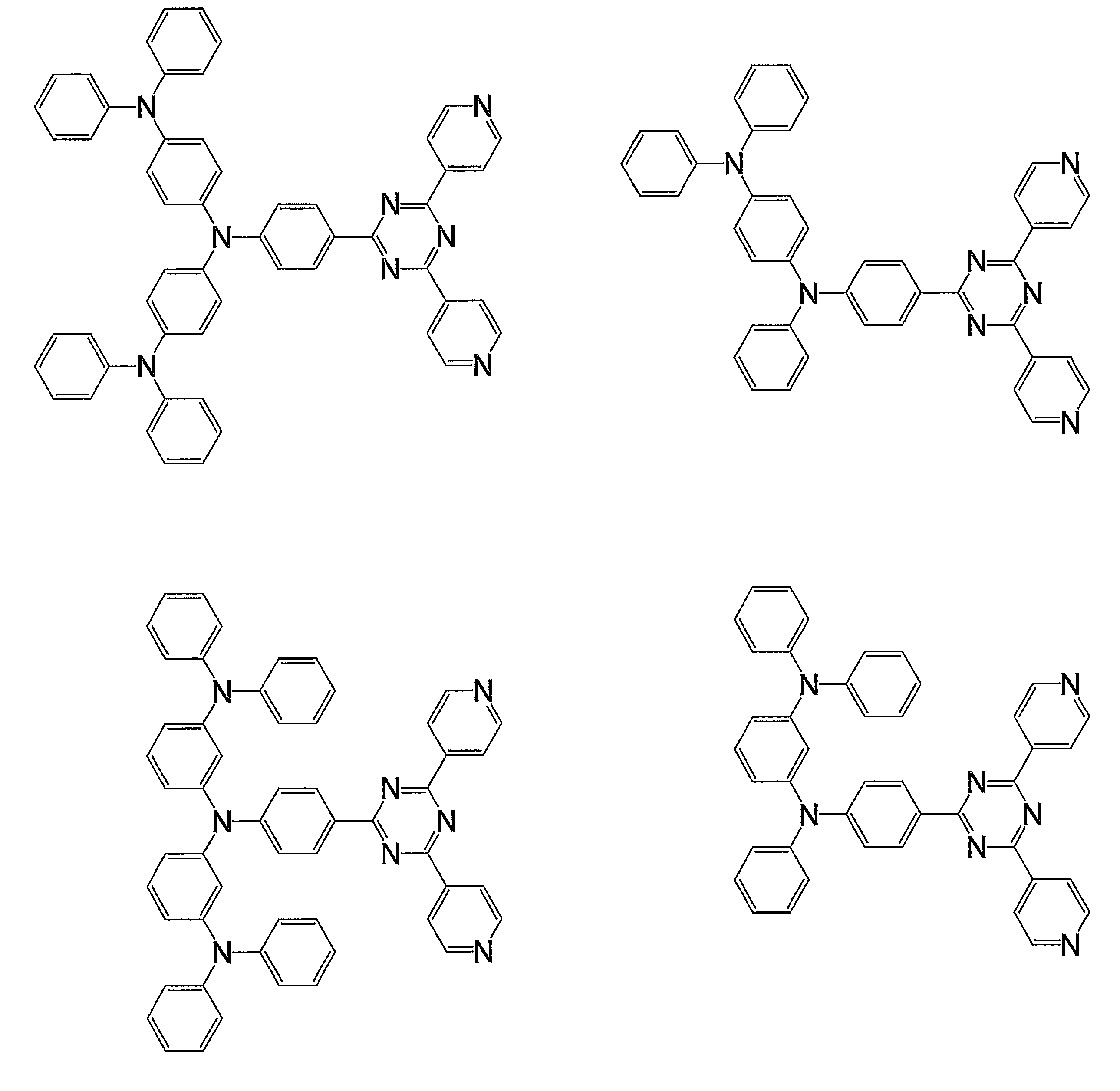
以下において、一般式(1)で表される化合物の具体例を例示する。ただし、本発明において用いることができる一般式(1)で表される化合物はこれらの具体例によって限定的に解釈されるべきものではない。


一般式(1)で表される化合物の分子量は、例えば一般式(1)で表される化合物を含む有機層を蒸着法により製膜して利用することを意図する場合には、1500以下であることが好ましく、1200以下であることがより好ましく、1000以下であることがさらに好ましく、800以下であることがさらにより好ましい。分子量の下限値は、一般式(1)で表される最小化合物の分子量である。
一般式(1)で表される化合物は、分子量にかかわらず塗布法で成膜してもよい。塗布法を用いれば、分子量が比較的大きな化合物であっても成膜することが可能である。
一般式(1)で表される化合物は、分子量にかかわらず塗布法で成膜してもよい。塗布法を用いれば、分子量が比較的大きな化合物であっても成膜することが可能である。
本発明を応用して、分子内に一般式(1)で表される構造を複数個含む化合物を、発光材料として用いることも考えられる。
例えば、一般式(1)で表される構造中にあらかじめ重合性基を存在させておいて、その重合性基を重合させることによって得られる重合体を、発光材料として用いることが考えられる。具体的には、一般式(1)のAr1、Ar2、Ar3、D1、D2、D3のいずれかに重合性官能基を含むモノマーを用意して、これを単独で重合させるか、他のモノマーとともに共重合させることにより、繰り返し単位を有する重合体を得て、その重合体を発光材料として用いることが考えられる。あるいは、一般式(1)で表される構造を有する化合物どうしをカップリングさせることにより、二量体や三量体を得て、それらを発光材料として用いることも考えられる。
例えば、一般式(1)で表される構造中にあらかじめ重合性基を存在させておいて、その重合性基を重合させることによって得られる重合体を、発光材料として用いることが考えられる。具体的には、一般式(1)のAr1、Ar2、Ar3、D1、D2、D3のいずれかに重合性官能基を含むモノマーを用意して、これを単独で重合させるか、他のモノマーとともに共重合させることにより、繰り返し単位を有する重合体を得て、その重合体を発光材料として用いることが考えられる。あるいは、一般式(1)で表される構造を有する化合物どうしをカップリングさせることにより、二量体や三量体を得て、それらを発光材料として用いることも考えられる。
一般式(1)で表される構造を含む繰り返し単位を有する重合体の例として、下記一般式(3)または(4)で表される構造を含む重合体を挙げることができる。
一般式(3)および(4)において、Qは一般式(1)で表される構造を含む基を表し、L1およびL2は連結基を表す。連結基の炭素数は、好ましくは0~20であり、より好ましくは1~15であり、さらに好ましくは2~10である。連結基は-X11-L11-で表される構造を有するものであることが好ましい。ここで、X11は酸素原子または硫黄原子を表し、酸素原子であることが好ましい。L11は連結基を表し、置換もしくは無置換のアルキレン基、または置換もしくは無置換のアリーレン基であることが好ましく、炭素数1~10の置換もしくは無置換のアルキレン基、または置換もしくは無置換のフェニレン基であることがより好ましい。
一般式(3)および(4)において、R101、R102、R103およびR104は、各々独立に置換基を表す。好ましくは、炭素数1~6の置換もしくは無置換のアルキル基、炭素数1~6の置換もしくは無置換のアルコキシ基、ハロゲン原子であり、より好ましくは炭素数1~3の無置換のアルキル基、炭素数1~3の無置換のアルコキシ基、フッ素原子、塩素原子であり、さらに好ましくは炭素数1~3の無置換のアルキル基、炭素数1~3の無置換のアルコキシ基である。
L1およびL2で表される連結基は、Qを構成する一般式(1)の構造のAr1、Ar2、Ar3、D1、D2、D3のいずれか、一般式(2)のR1~R12、R14~R25のいずれかに結合することができる。1つのQに対して連結基が2つ以上連結して架橋構造や網目構造を形成していてもよい。
繰り返し単位の具体的な構造例として、下記式(5)~(8)で表される構造を挙げることができる。

これらの式(5)~(8)を含む繰り返し単位を有する重合体は、一般式(1)の構造のAかDのいずれかにヒドロキシ基を導入しておき、それをリンカーとして下記化合物を反応させて重合性基を導入し、その重合性基を重合させることにより合成することができる。

分子内に一般式(1)で表される構造を含む重合体は、一般式(1)で表される構造を有する繰り返し単位のみからなる重合体であってもよいし、それ以外の構造を有する繰り返し単位を含む重合体であってもよい。また、重合体の中に含まれる一般式(1)で表される構造を有する繰り返し単位は、単一種であってもよいし、2種以上であってもよい。一般式(1)で表される構造を有さない繰り返し単位としては、通常の共重合に用いられるモノマーから誘導されるものを挙げることができる。例えば、エチレン、スチレンなどのエチレン性不飽和結合を有するモノマーから誘導される繰り返し単位を挙げることができる。
[一般式(1)で表される化合物の合成方法]
一般式(1)で表される化合物は、既知の反応を組み合わせることによって合成することができる。例えば、以下のスキームにしたがって合成することが可能である。

一般式(1)で表される化合物は、既知の反応を組み合わせることによって合成することができる。例えば、以下のスキームにしたがって合成することが可能である。
上記のスキームにおけるAr1、Ar2、Ar3、D2、D3の説明については、一般式(1)における対応する記載を参照することができる。D1は、群1-1から選択される基で置換されたジアリールアミノ基を表す。Xはハロゲン原子を表し、フッ素原子、塩素原子、臭素原子、ヨウ素原子を挙げることができ、塩素原子、臭素原子、ヨウ素原子が好ましい。
上記のスキームにおける反応は、公知のカップリング反応を応用したものであり、公知の反応条件を適宜選択して用いることができる。上記の反応の詳細については、後述の合成例を参考にすることができる。また、一般式(1)で表される化合物は、その他の公知の合成反応を組み合わせることによっても合成することができる。
上記のスキームにおける反応は、公知のカップリング反応を応用したものであり、公知の反応条件を適宜選択して用いることができる。上記の反応の詳細については、後述の合成例を参考にすることができる。また、一般式(1)で表される化合物は、その他の公知の合成反応を組み合わせることによっても合成することができる。
[有機発光素子]
本発明の一般式(1)で表される化合物は、有機発光素子の発光材料として有用である。このため、本発明の一般式(1)で表される化合物は、有機発光素子の発光層に発光材料として効果的に用いることができる。一般式(1)で表される化合物の中には、遅延蛍光を放射する遅延蛍光材料(遅延蛍光体)が含まれている。すなわち本発明は、一般式(1)で表される構造を有する遅延蛍光体の発明と、一般式(1)で表される化合物を遅延蛍光体として使用する発明と、一般式(1)で表される化合物を用いて遅延蛍光を発光させる方法の発明も提供する。そのような化合物を発光材料として用いた有機発光素子は、遅延蛍光を放射し、発光効率が高いという特徴を有する。その原理を、有機エレクトロルミネッセンス素子を例にとって説明すると以下のようになる。
本発明の一般式(1)で表される化合物は、有機発光素子の発光材料として有用である。このため、本発明の一般式(1)で表される化合物は、有機発光素子の発光層に発光材料として効果的に用いることができる。一般式(1)で表される化合物の中には、遅延蛍光を放射する遅延蛍光材料(遅延蛍光体)が含まれている。すなわち本発明は、一般式(1)で表される構造を有する遅延蛍光体の発明と、一般式(1)で表される化合物を遅延蛍光体として使用する発明と、一般式(1)で表される化合物を用いて遅延蛍光を発光させる方法の発明も提供する。そのような化合物を発光材料として用いた有機発光素子は、遅延蛍光を放射し、発光効率が高いという特徴を有する。その原理を、有機エレクトロルミネッセンス素子を例にとって説明すると以下のようになる。
有機エレクトロルミネッセンス素子においては、正負の両電極より発光材料にキャリアを注入し、励起状態の発光材料を生成し、発光させる。通常、キャリア注入型の有機エレクトロルミネッセンス素子の場合、生成した励起子のうち、励起一重項状態に励起されるのは25%であり、残り75%は励起三重項状態に励起される。従って、励起三重項状態からの発光であるリン光を利用するほうが、エネルギーの利用効率が高い。しかしながら、励起三重項状態は寿命が長いため、励起状態の飽和や励起三重項状態の励起子との相互作用によるエネルギーの失活が起こり、一般にリン光の量子収率が高くないことが多い。一方、遅延蛍光材料は、項間交差等により励起三重項状態へとエネルギーが遷移した後、三重項-三重項消滅あるいは熱エネルギーの吸収により、励起一重項状態に逆項間交差され蛍光を放射する。有機エレクトロルミネッセンス素子においては、なかでも熱エネルギーの吸収による熱活性化型の遅延蛍光材料が特に有用であると考えられる。有機エレクトロルミネッセンス素子に遅延蛍光材料を利用した場合、励起一重項状態の励起子は通常通り蛍光を放射する。一方、励起三重項状態の励起子は、デバイスが発する熱を吸収して励起一重項へ項間交差され蛍光を放射する。このとき、励起一重項からの発光であるため蛍光と同波長での発光でありながら、励起三重項状態から励起一重項状態への逆項間交差により、生じる光の寿命(発光寿命)は通常の蛍光やりん光よりも長くなるため、これらよりも遅延した蛍光として観察される。これを遅延蛍光として定義できる。このような熱活性化型の励起子移動機構を用いれば、キャリア注入後に熱エネルギーの吸収を経ることにより、通常は25%しか生成しなかった励起一重項状態の化合物の比率を25%以上に引き上げることが可能となる。100℃未満の低い温度でも強い蛍光および遅延蛍光を発する化合物を用いれば、デバイスの熱で充分に励起三重項状態から励起一重項状態への項間交差が生じて遅延蛍光を放射するため、発光効率を飛躍的に向上させることができる。
本発明の一般式(1)で表される化合物を発光層の発光材料として用いることにより、有機フォトルミネッセンス素子(有機PL素子)や有機エレクトロルミネッセンス素子(有機EL素子)などの優れた有機発光素子を提供することができる。このとき、本発明の一般式(1)で表される化合物は、いわゆるアシストドーパントとして、発光層に含まれる他の発光材料の発光をアシストする機能を有するものであってもよい。すなわち、発光層に含まれる本発明の一般式(1)で表される化合物は、発光層に含まれるホスト材料の最低励起一重項エネルギー準位と発光層に含まれる他の発光材料の最低励起一重項エネルギー準位の間の最低励起一重項エネルギー準位を有するものであってもよい。
有機フォトルミネッセンス素子は、基板上に少なくとも発光層を形成した構造を有する。また、有機エレクトロルミネッセンス素子は、少なくとも陽極、陰極、および陽極と陰極の間に有機層を形成した構造を有する。有機層は、少なくとも発光層を含むものであり、発光層のみからなるものであってもよいし、発光層の他に1層以上の有機層を有するものであってもよい。そのような他の有機層として、正孔輸送層、正孔注入層、電子阻止層、正孔阻止層、電子注入層、電子輸送層、励起子阻止層などを挙げることができる。正孔輸送層は正孔注入機能を有した正孔注入輸送層でもよく、電子輸送層は電子注入機能を有した電子注入輸送層でもよい。具体的な有機エレクトロルミネッセンス素子の構造例を図1に示す。図1において、1は基板、2は陽極、3は正孔注入層、4は正孔輸送層、5は発光層、6は電子輸送層、7は陰極を表わす。
以下において、有機エレクトロルミネッセンス素子の各部材および各層について説明する。なお、基板と発光層の説明は有機フォトルミネッセンス素子の基板と発光層にも該当する。
(基板)
本発明の有機エレクトロルミネッセンス素子は、基板に支持されていることが好ましい。この基板については、特に制限はなく、従来から有機エレクトロルミネッセンス素子に慣用されているものであればよく、例えば、ガラス、透明プラスチック、石英、シリコンなどからなるものを用いることができる。
本発明の有機エレクトロルミネッセンス素子は、基板に支持されていることが好ましい。この基板については、特に制限はなく、従来から有機エレクトロルミネッセンス素子に慣用されているものであればよく、例えば、ガラス、透明プラスチック、石英、シリコンなどからなるものを用いることができる。
(陽極)
有機エレクトロルミネッセンス素子における陽極としては、仕事関数の大きい(4eV以上)金属、合金、電気伝導性化合物およびこれらの混合物を電極材料とするものが好ましく用いられる。このような電極材料の具体例としてはAu等の金属、CuI、インジウムチンオキシド(ITO)、SnO2、ZnO等の導電性透明材料が挙げられる。また、IDIXO(In2O3-ZnO)等非晶質で透明導電膜を作製可能な材料を用いてもよい。陽極はこれらの電極材料を蒸着やスパッタリング等の方法により、薄膜を形成させ、フォトリソグラフィー法で所望の形状のパターンを形成してもよく、あるいはパターン精度をあまり必要としない場合は(100μm以上程度)、上記電極材料の蒸着やスパッタリング時に所望の形状のマスクを介してパターンを形成してもよい。あるいは、有機導電性化合物のように塗布可能な材料を用いる場合には、印刷方式、コーティング方式等湿式成膜法を用いることもできる。この陽極より発光を取り出す場合には、透過率を10%より大きくすることが望ましく、また陽極としてのシート抵抗は数百Ω/□以下が好ましい。さらに膜厚は材料にもよるが、通常10~1000nm、好ましくは10~200nmの範囲で選ばれる。
有機エレクトロルミネッセンス素子における陽極としては、仕事関数の大きい(4eV以上)金属、合金、電気伝導性化合物およびこれらの混合物を電極材料とするものが好ましく用いられる。このような電極材料の具体例としてはAu等の金属、CuI、インジウムチンオキシド(ITO)、SnO2、ZnO等の導電性透明材料が挙げられる。また、IDIXO(In2O3-ZnO)等非晶質で透明導電膜を作製可能な材料を用いてもよい。陽極はこれらの電極材料を蒸着やスパッタリング等の方法により、薄膜を形成させ、フォトリソグラフィー法で所望の形状のパターンを形成してもよく、あるいはパターン精度をあまり必要としない場合は(100μm以上程度)、上記電極材料の蒸着やスパッタリング時に所望の形状のマスクを介してパターンを形成してもよい。あるいは、有機導電性化合物のように塗布可能な材料を用いる場合には、印刷方式、コーティング方式等湿式成膜法を用いることもできる。この陽極より発光を取り出す場合には、透過率を10%より大きくすることが望ましく、また陽極としてのシート抵抗は数百Ω/□以下が好ましい。さらに膜厚は材料にもよるが、通常10~1000nm、好ましくは10~200nmの範囲で選ばれる。
(陰極)
一方、陰極としては、仕事関数の小さい(4eV以下)金属(電子注入性金属と称する)、合金、電気伝導性化合物およびこれらの混合物を電極材料とするものが用いられる。このような電極材料の具体例としては、ナトリウム、ナトリウム-カリウム合金、マグネシウム、リチウム、マグネシウム/銅混合物、マグネシウム/銀混合物、マグネシウム/アルミニウム混合物、マグネシウム/インジウム混合物、アルミニウム/酸化アルミニウム(Al2O3)混合物、インジウム、リチウム/アルミニウム混合物、希土類金属等が挙げられる。これらの中で、電子注入性および酸化等に対する耐久性の点から、電子注入性金属とこれより仕事関数の値が大きく安定な金属である第二金属との混合物、例えば、マグネシウム/銀混合物、マグネシウム/アルミニウム混合物、マグネシウム/インジウム混合物、アルミニウム/酸化アルミニウム(Al2O3)混合物、リチウム/アルミニウム混合物、アルミニウム等が好適である。陰極はこれらの電極材料を蒸着やスパッタリング等の方法により薄膜を形成させることにより、作製することができる。また、陰極としてのシート抵抗は数百Ω/□以下が好ましく、膜厚は通常10nm~5μm、好ましくは50~200nmの範囲で選ばれる。なお、発光した光を透過させるため、有機エレクトロルミネッセンス素子の陽極または陰極のいずれか一方が、透明または半透明であれば発光輝度が向上し好都合である。
また、陽極の説明で挙げた導電性透明材料を陰極に用いることで、透明または半透明の陰極を作製することができ、これを応用することで陽極と陰極の両方が透過性を有する素子を作製することができる。
(発光層)
発光層は、陽極および陰極のそれぞれから注入された正孔および電子が再結合することにより励起子が生成した後、発光する層であり、発光材料を単独で発光層に使用しても良いが、好ましくは発光材料とホスト材料を含む。発光材料としては、一般式(1)で表される本発明の化合物群から選ばれる1種または2種以上を用いることができる。本発明の有機エレクトロルミネッセンス素子および有機フォトルミネッセンス素子が高い発光効率を発現するためには、発光材料に生成した一重項励起子および三重項励起子を、発光材料中に閉じ込めることが重要である。従って、発光層中に発光材料に加えてホスト材料を用いることが好ましい。ホスト材料としては、励起一重項エネルギー、励起三重項エネルギーの少なくとも何れか一方が本発明の発光材料よりも高い値を有する有機化合物を用いることができる。その結果、本発明の発光材料に生成した一重項励起子および三重項励起子を、本発明の発光材料の分子中に閉じ込めることが可能となり、その発光効率を十分に引き出すことが可能となる。もっとも、一重項励起子および三重項励起子を十分に閉じ込めることができなくても、高い発光効率を得ることが可能な場合もあるため、高い発光効率を実現しうるホスト材料であれば特に制約なく本発明に用いることができる。本発明の有機発光素子または有機エレクトロルミネッセンス素子において、発光は発光層に含まれる本発明の発光材料から生じる。この発光は蛍光発光および遅延蛍光発光の両方を含む。但し、発光の一部或いは部分的にホスト材料からの発光があってもかまわない。
ホスト材料を用いる場合、発光材料である本発明の化合物が発光層中に含有される量は0.1重量%以上であることが好ましく、1重量%以上であることがより好ましく、また、50重量%以下であることが好ましく、20重量%以下であることがより好ましく、10重量%以下であることがさらに好ましい。
発光層におけるホスト材料としては、正孔輸送能、電子輸送能を有し、かつ発光の長波長化を防ぎ、なおかつ高いガラス転移温度を有する有機化合物であることが好ましい。
(注入層)
注入層とは、駆動電圧低下や発光輝度向上のために電極と有機層間に設けられる層のことで、正孔注入層と電子注入層があり、陽極と発光層または正孔輸送層の間、および陰極と発光層または電子輸送層との間に存在させてもよい。注入層は必要に応じて設けることができる。
注入層とは、駆動電圧低下や発光輝度向上のために電極と有機層間に設けられる層のことで、正孔注入層と電子注入層があり、陽極と発光層または正孔輸送層の間、および陰極と発光層または電子輸送層との間に存在させてもよい。注入層は必要に応じて設けることができる。
(阻止層)
阻止層は、発光層中に存在する電荷(電子もしくは正孔)および/または励起子の発光層外への拡散を阻止することができる層である。電子阻止層は、発光層および正孔輸送層の間に配置されることができ、電子が正孔輸送層の方に向かって発光層を通過することを阻止する。同様に、正孔阻止層は発光層および電子輸送層の間に配置されることができ、正孔が電子輸送層の方に向かって発光層を通過することを阻止する。阻止層はまた、励起子が発光層の外側に拡散することを阻止するために用いることができる。すなわち電子阻止層、正孔阻止層はそれぞれ励起子阻止層としての機能も兼ね備えることができる。本明細書でいう電子阻止層または励起子阻止層は、一つの層で電子阻止層および励起子阻止層の機能を有する層を含む意味で使用される。
阻止層は、発光層中に存在する電荷(電子もしくは正孔)および/または励起子の発光層外への拡散を阻止することができる層である。電子阻止層は、発光層および正孔輸送層の間に配置されることができ、電子が正孔輸送層の方に向かって発光層を通過することを阻止する。同様に、正孔阻止層は発光層および電子輸送層の間に配置されることができ、正孔が電子輸送層の方に向かって発光層を通過することを阻止する。阻止層はまた、励起子が発光層の外側に拡散することを阻止するために用いることができる。すなわち電子阻止層、正孔阻止層はそれぞれ励起子阻止層としての機能も兼ね備えることができる。本明細書でいう電子阻止層または励起子阻止層は、一つの層で電子阻止層および励起子阻止層の機能を有する層を含む意味で使用される。
(正孔阻止層)
正孔阻止層とは広い意味では電子輸送層の機能を有する。正孔阻止層は電子を輸送しつつ、正孔が電子輸送層へ到達することを阻止する役割があり、これにより発光層中での電子と正孔の再結合確率を向上させることができる。正孔阻止層の材料としては、後述する電子輸送層の材料を必要に応じて用いることができる。
正孔阻止層とは広い意味では電子輸送層の機能を有する。正孔阻止層は電子を輸送しつつ、正孔が電子輸送層へ到達することを阻止する役割があり、これにより発光層中での電子と正孔の再結合確率を向上させることができる。正孔阻止層の材料としては、後述する電子輸送層の材料を必要に応じて用いることができる。
(電子阻止層)
電子阻止層とは、広い意味では正孔を輸送する機能を有する。電子阻止層は正孔を輸送しつつ、電子が正孔輸送層へ到達することを阻止する役割があり、これにより発光層中での電子と正孔が再結合する確率を向上させることができる。
電子阻止層とは、広い意味では正孔を輸送する機能を有する。電子阻止層は正孔を輸送しつつ、電子が正孔輸送層へ到達することを阻止する役割があり、これにより発光層中での電子と正孔が再結合する確率を向上させることができる。
(励起子阻止層)
励起子阻止層とは、発光層内で正孔と電子が再結合することにより生じた励起子が電荷輸送層に拡散することを阻止するための層であり、本層の挿入により励起子を効率的に発光層内に閉じ込めることが可能となり、素子の発光効率を向上させることができる。励起子阻止層は発光層に隣接して陽極側、陰極側のいずれにも挿入することができ、両方同時に挿入することも可能である。すなわち、励起子阻止層を陽極側に有する場合、正孔輸送層と発光層の間に、発光層に隣接して該層を挿入することができ、陰極側に挿入する場合、発光層と陰極との間に、発光層に隣接して該層を挿入することができる。また、陽極と、発光層の陽極側に隣接する励起子阻止層との間には、正孔注入層や電子阻止層などを有することができ、陰極と、発光層の陰極側に隣接する励起子阻止層との間には、電子注入層、電子輸送層、正孔阻止層などを有することができる。阻止層を配置する場合、阻止層として用いる材料の励起一重項エネルギーおよび励起三重項エネルギーの少なくともいずれか一方は、発光材料の励起一重項エネルギーおよび励起三重項エネルギーよりも高いことが好ましい。
励起子阻止層とは、発光層内で正孔と電子が再結合することにより生じた励起子が電荷輸送層に拡散することを阻止するための層であり、本層の挿入により励起子を効率的に発光層内に閉じ込めることが可能となり、素子の発光効率を向上させることができる。励起子阻止層は発光層に隣接して陽極側、陰極側のいずれにも挿入することができ、両方同時に挿入することも可能である。すなわち、励起子阻止層を陽極側に有する場合、正孔輸送層と発光層の間に、発光層に隣接して該層を挿入することができ、陰極側に挿入する場合、発光層と陰極との間に、発光層に隣接して該層を挿入することができる。また、陽極と、発光層の陽極側に隣接する励起子阻止層との間には、正孔注入層や電子阻止層などを有することができ、陰極と、発光層の陰極側に隣接する励起子阻止層との間には、電子注入層、電子輸送層、正孔阻止層などを有することができる。阻止層を配置する場合、阻止層として用いる材料の励起一重項エネルギーおよび励起三重項エネルギーの少なくともいずれか一方は、発光材料の励起一重項エネルギーおよび励起三重項エネルギーよりも高いことが好ましい。
(正孔輸送層)
正孔輸送層とは正孔を輸送する機能を有する正孔輸送材料からなり、正孔輸送層は単層または複数層設けることができる。
正孔輸送材料としては、正孔の注入または輸送、電子の障壁性のいずれかを有するものであり、有機物、無機物のいずれであってもよい。使用できる公知の正孔輸送材料としては例えば、トリアゾール誘導体、オキサジアゾール誘導体、イミダゾール誘導体、カルバゾール誘導体、インドロカルバゾール誘導体、ポリアリールアルカン誘導体、ピラゾリン誘導体およびピラゾロン誘導体、フェニレンジアミン誘導体、アリールアミン誘導体、アミノ置換カルコン誘導体、オキサゾール誘導体、スチリルアントラセン誘導体、フルオレノン誘導体、ヒドラゾン誘導体、スチルベン誘導体、シラザン誘導体、アニリン系共重合体、また導電性高分子オリゴマー、特にチオフェンオリゴマー等が挙げられるが、ポルフィリン化合物、芳香族第3級アミン化合物およびスチリルアミン化合物を用いることが好ましく、芳香族第3級アミン化合物を用いることがより好ましい。
(電子輸送層)
電子輸送層とは電子を輸送する機能を有する材料からなり、電子輸送層は単層または複数層設けることができる。
電子輸送材料(正孔阻止材料を兼ねる場合もある)としては、陰極より注入された電子を発光層に伝達する機能を有していればよい。使用できる電子輸送層としては例えば、ニトロ置換フルオレン誘導体、ジフェニルキノン誘導体、チオピランジオキシド誘導体、カルボジイミド、フレオレニリデンメタン誘導体、アントラキノジメタンおよびアントロン誘導体、オキサジアゾール誘導体等が挙げられる。さらに、上記オキサジアゾール誘導体において、オキサジアゾール環の酸素原子を硫黄原子に置換したチアジアゾール誘導体、電子吸引基として知られているキノキサリン環を有するキノキサリン誘導体も、電子輸送材料として用いることができる。さらにこれらの材料を高分子鎖に導入した、またはこれらの材料を高分子の主鎖とした高分子材料を用いることもできる。
有機エレクトロルミネッセンス素子を作製する際には、一般式(1)で表される化合物を発光層に用いるだけでなく、発光層以外の層にも用いてもよい。その際、発光層に用いる一般式(1)で表される化合物と、発光層以外の層に用いる一般式(1)で表される化合物は、同一であっても異なっていてもよい。例えば、上記の注入層、阻止層、正孔阻止層、電子阻止層、励起子阻止層、正孔輸送層、電子輸送層などにも一般式(1)で表される化合物を用いてもよい。これらの層の製膜方法は特に限定されず、ドライプロセス、ウェットプロセスのどちらで作製してもよい。
以下に、有機エレクトロルミネッセンス素子に用いることができる好ましい材料を具体的に例示する。ただし、本発明において用いることができる材料は、以下の例示化合物によって限定的に解釈されることはない。また、特定の機能を有する材料として例示した化合物であっても、その他の機能を有する材料として転用することも可能である。なお、以下の例示化合物の構造式におけるR、R2~R7は、各々独立に水素原子または置換基を表す。nは3~5の整数を表す。
まず、発光層のホスト材料としても用いることができる好ましい化合物を挙げる。
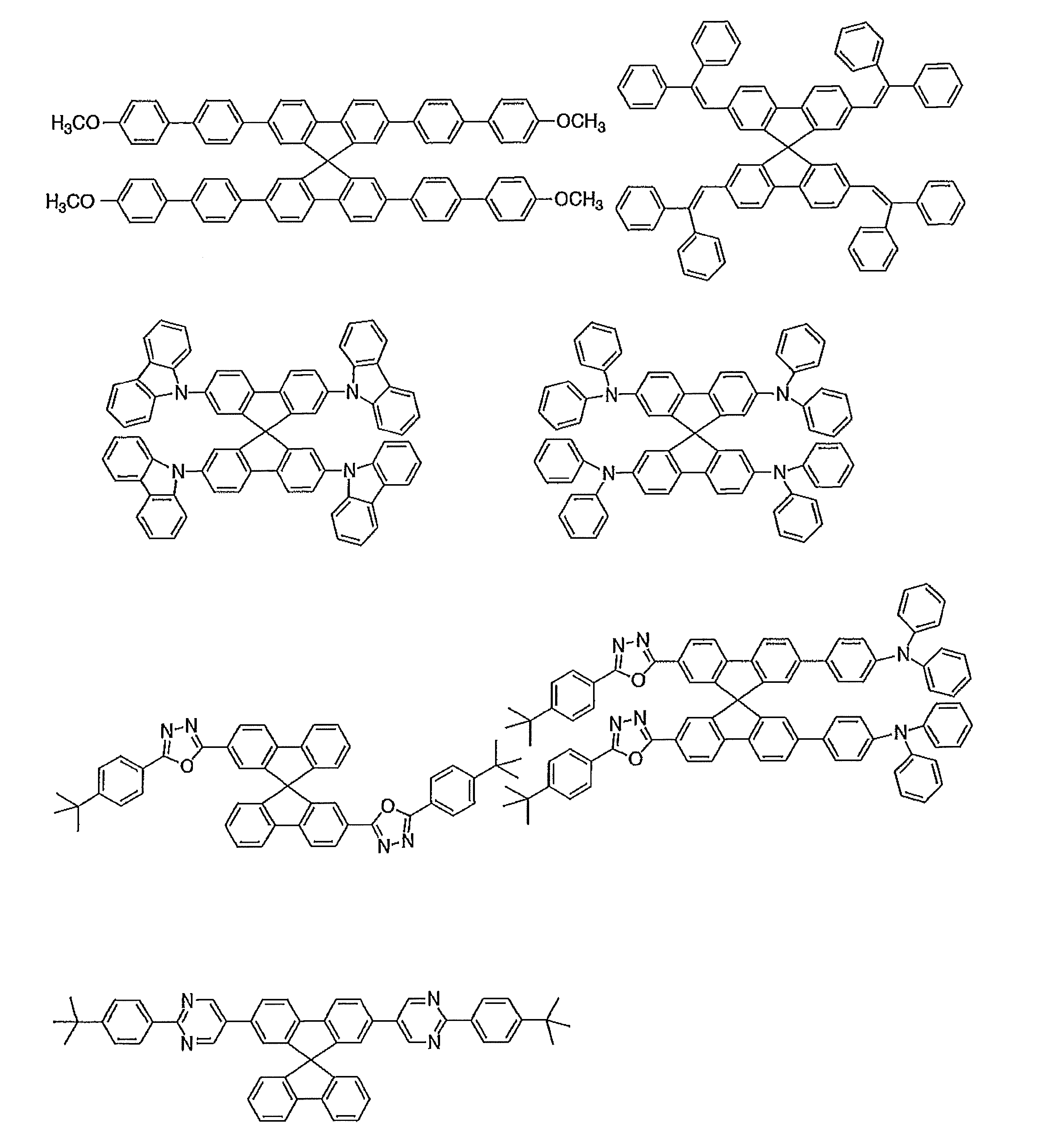
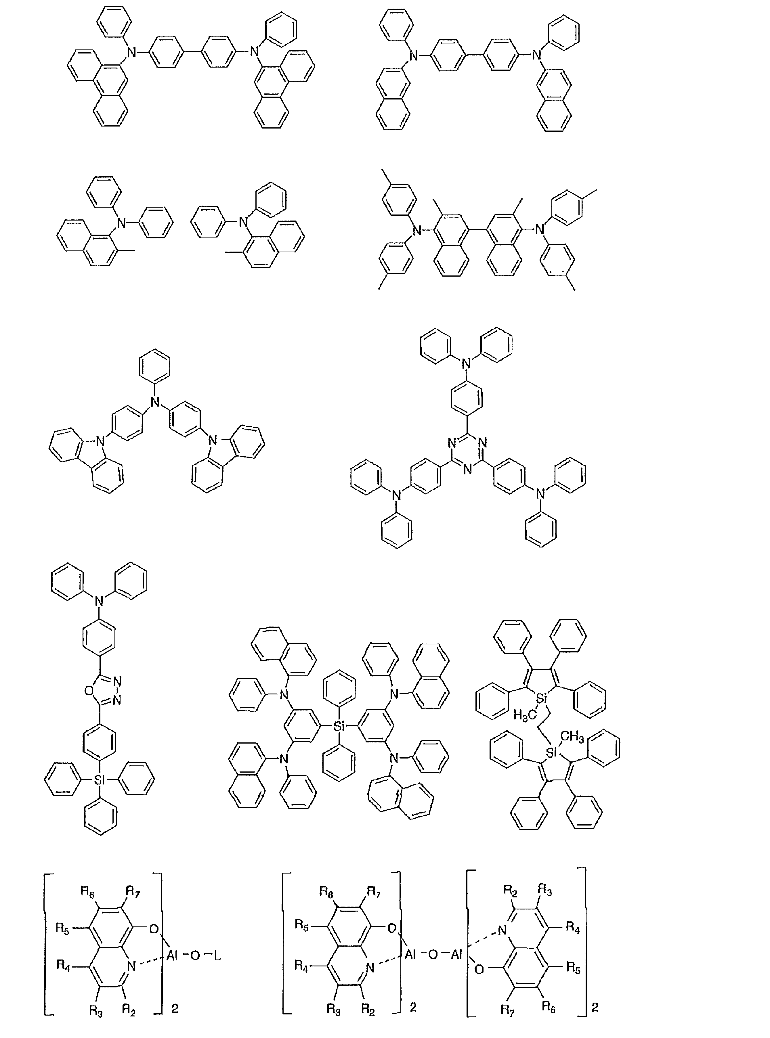


次に、正孔注入材料として用いることができる好ましい化合物例を挙げる。
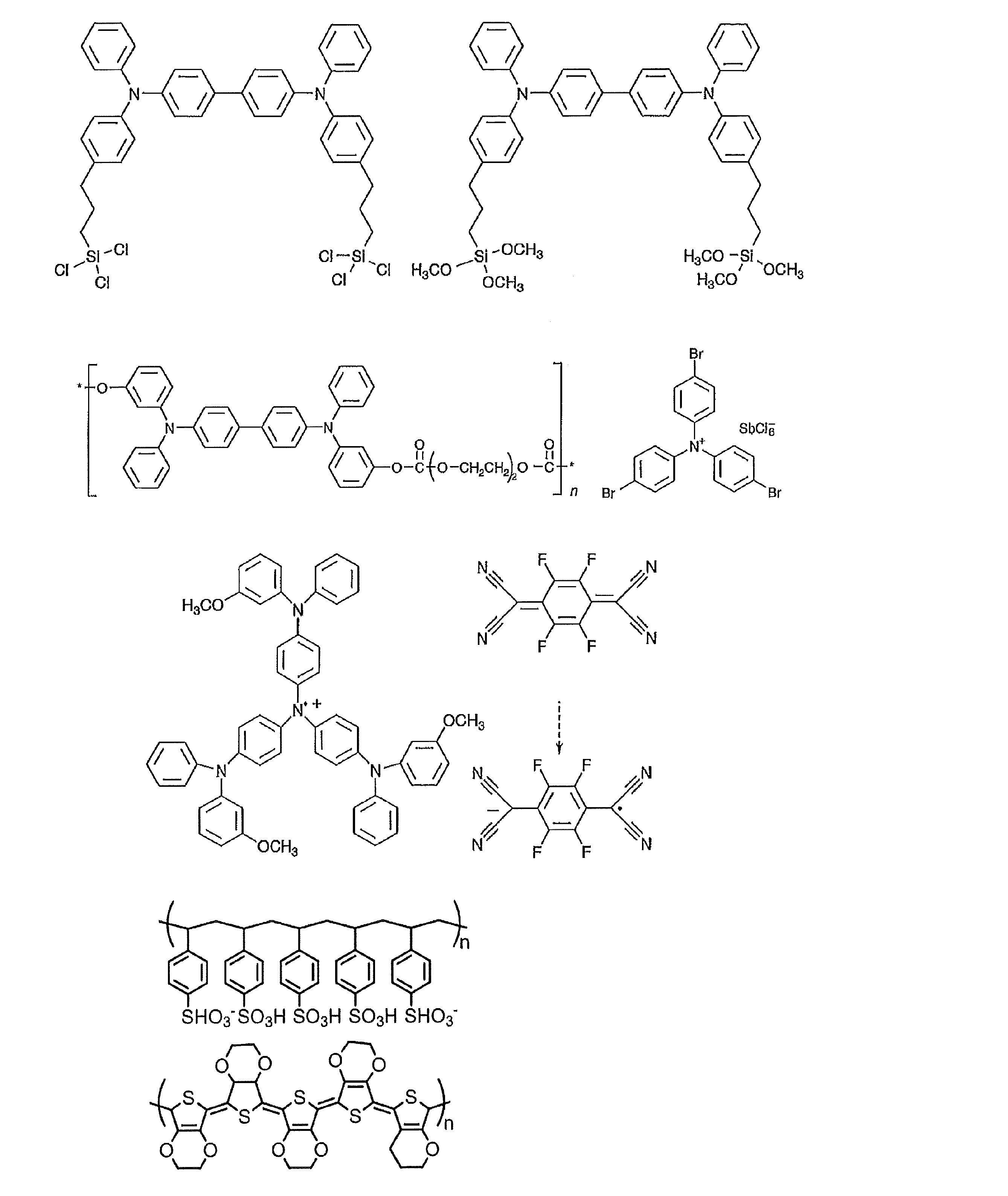
次に、正孔輸送材料として用いることができる好ましい化合物例を挙げる。

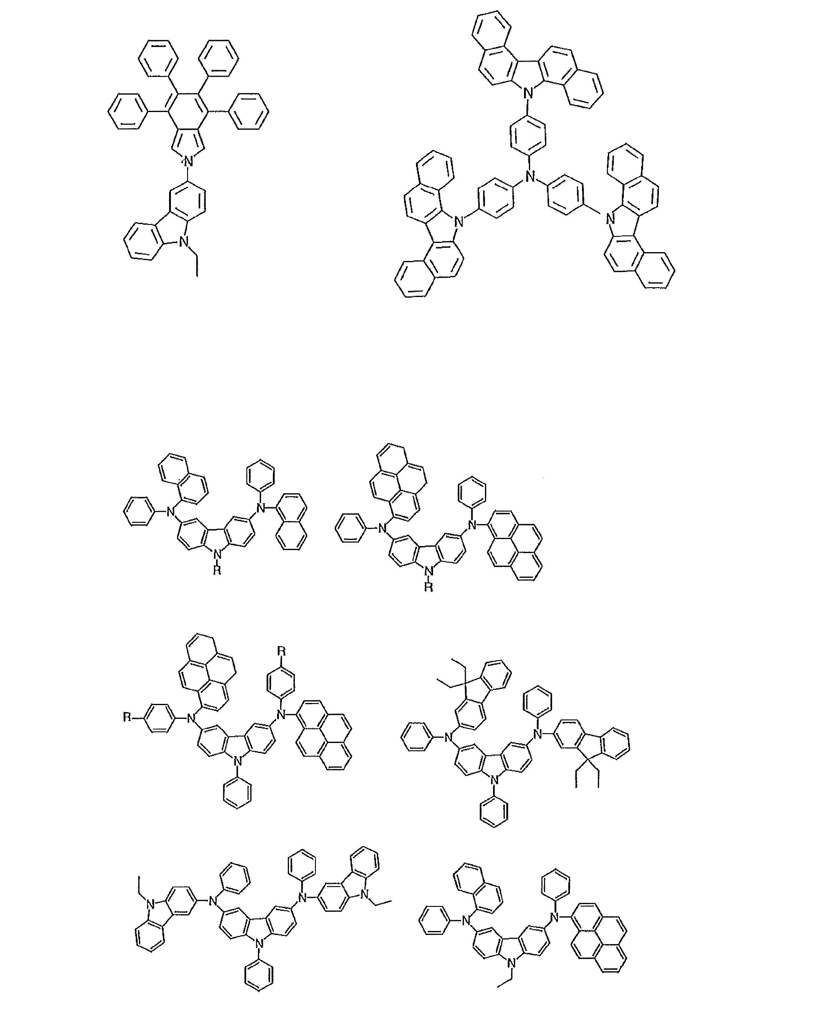
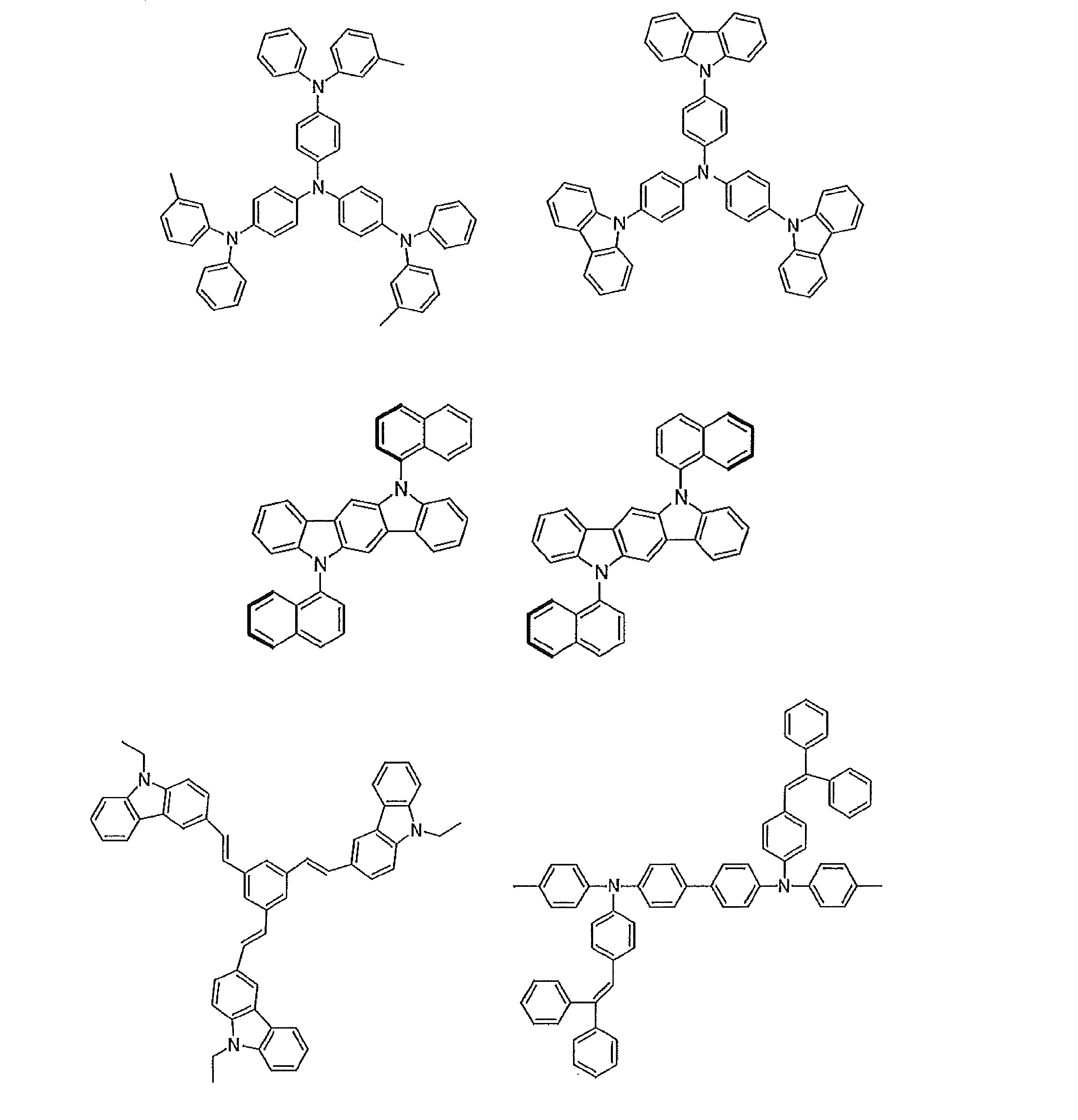

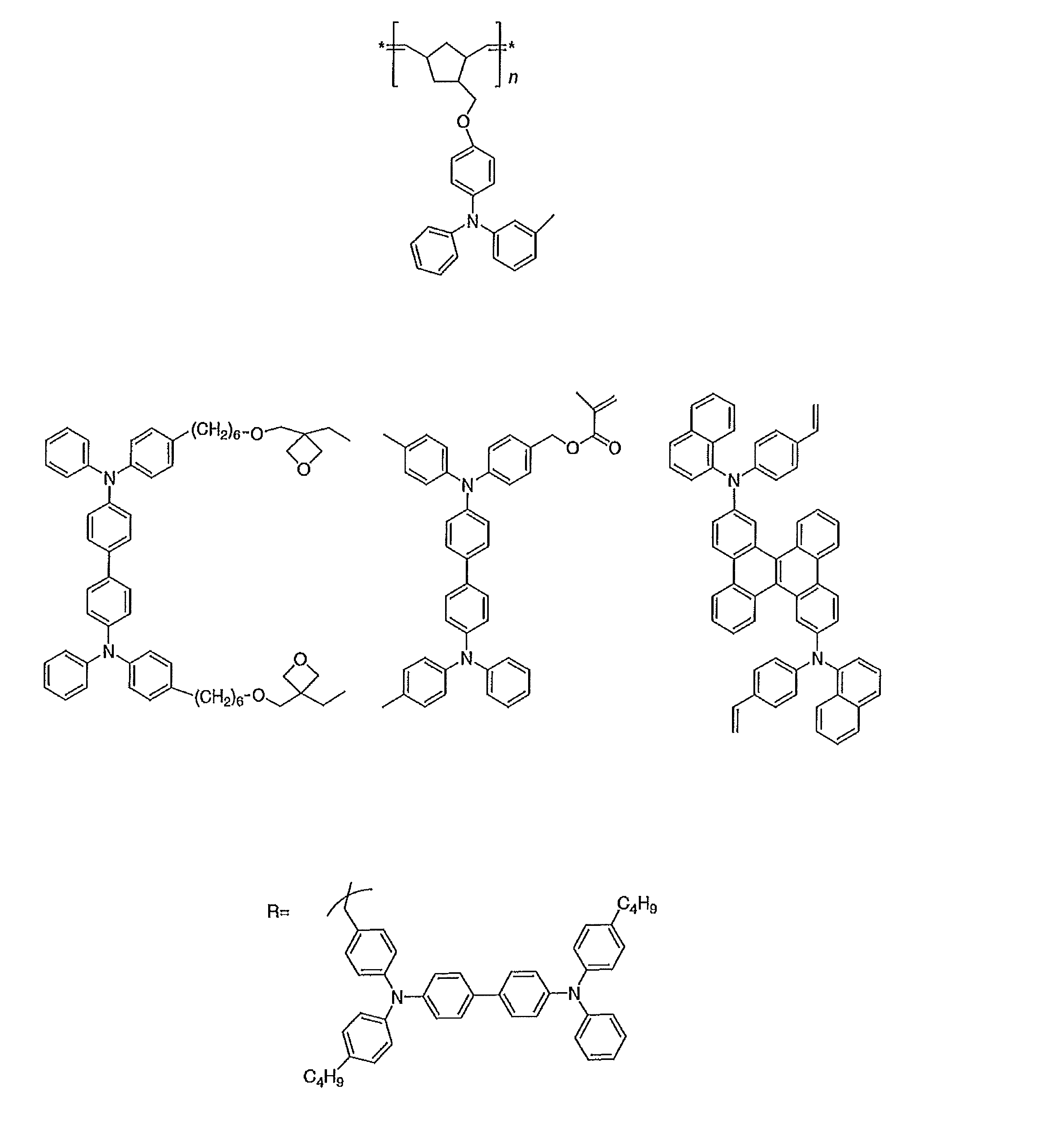
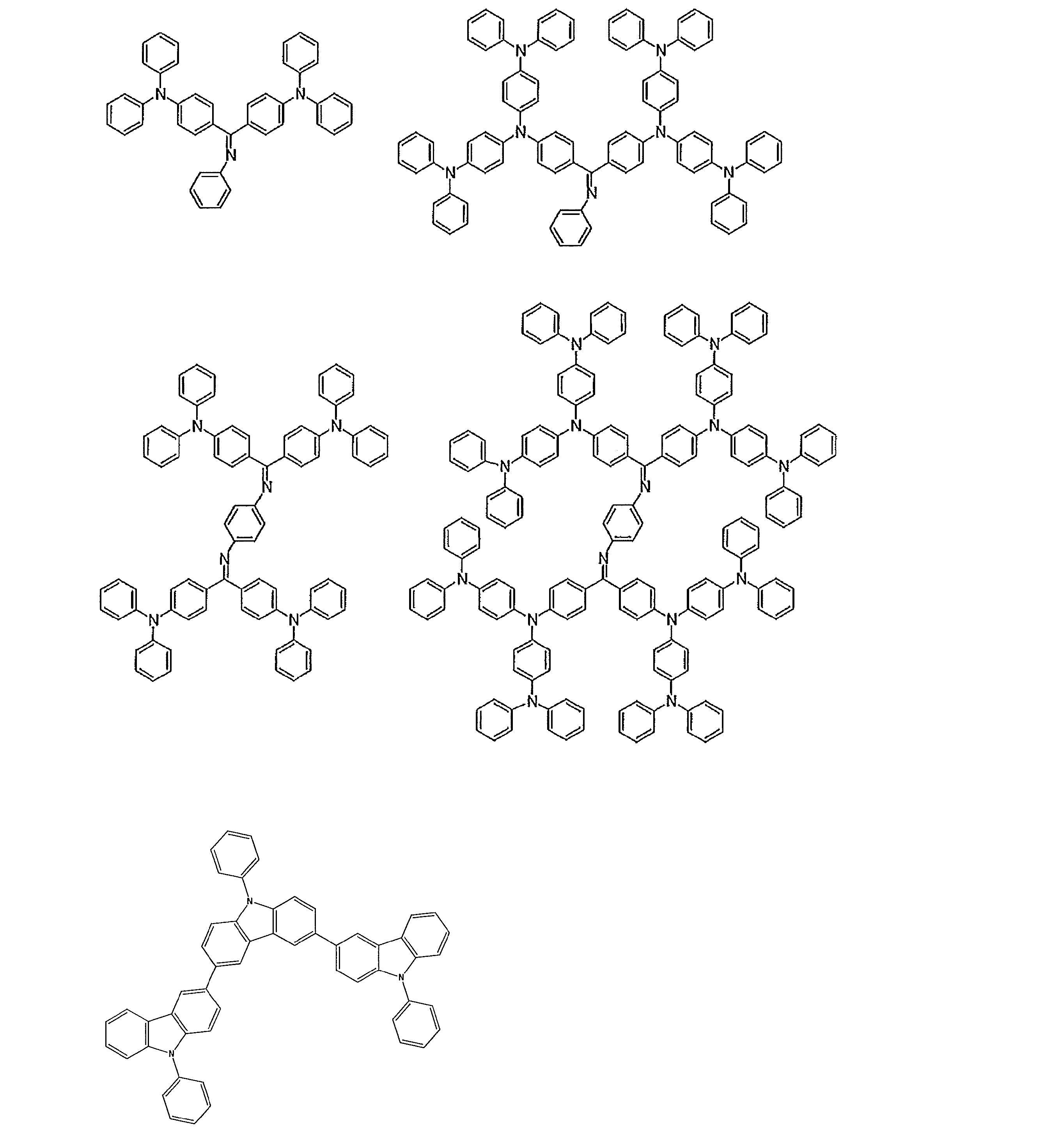
次に、電子阻止材料として用いることができる好ましい化合物例を挙げる。
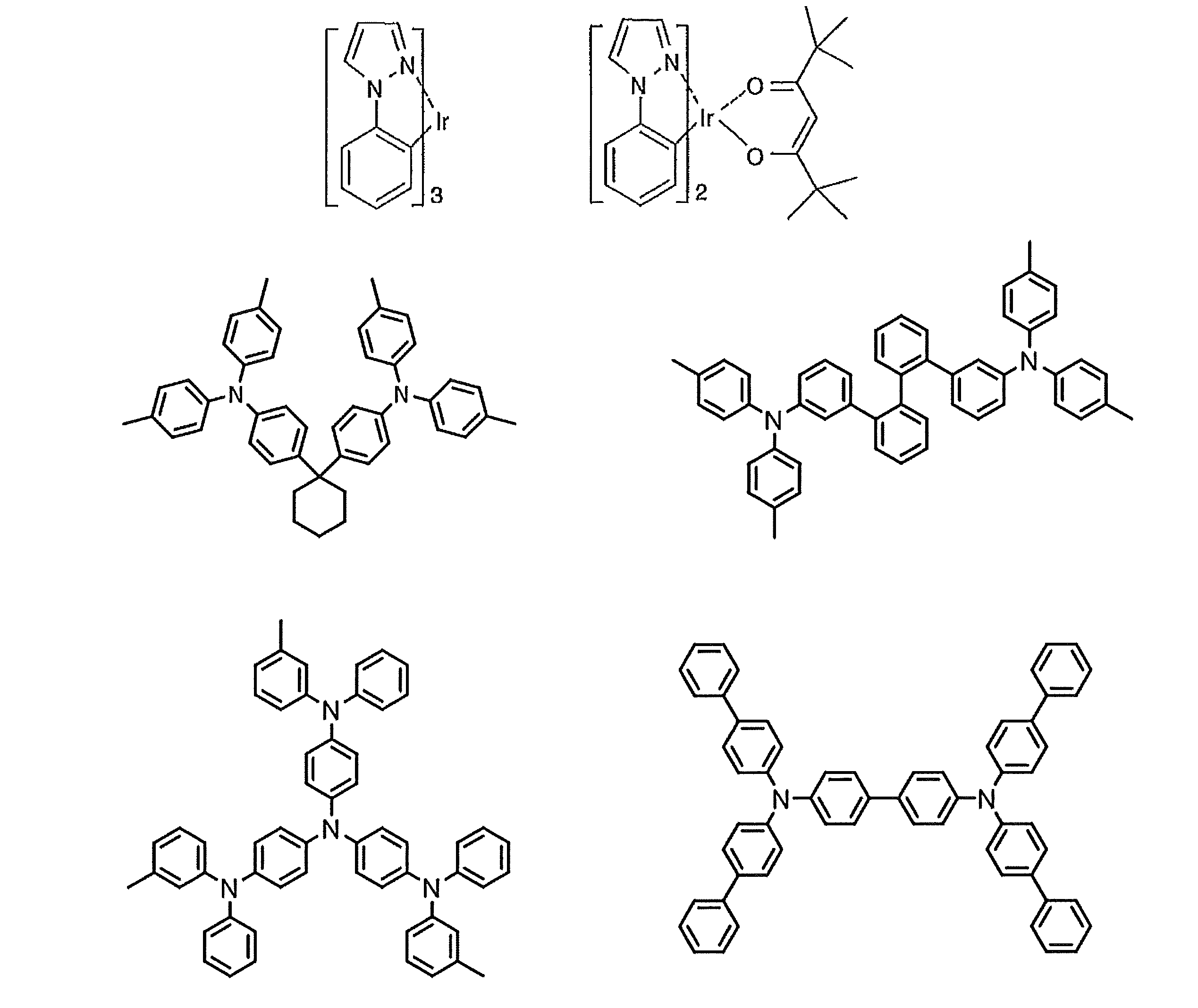
次に、正孔阻止材料として用いることができる好ましい化合物例を挙げる。
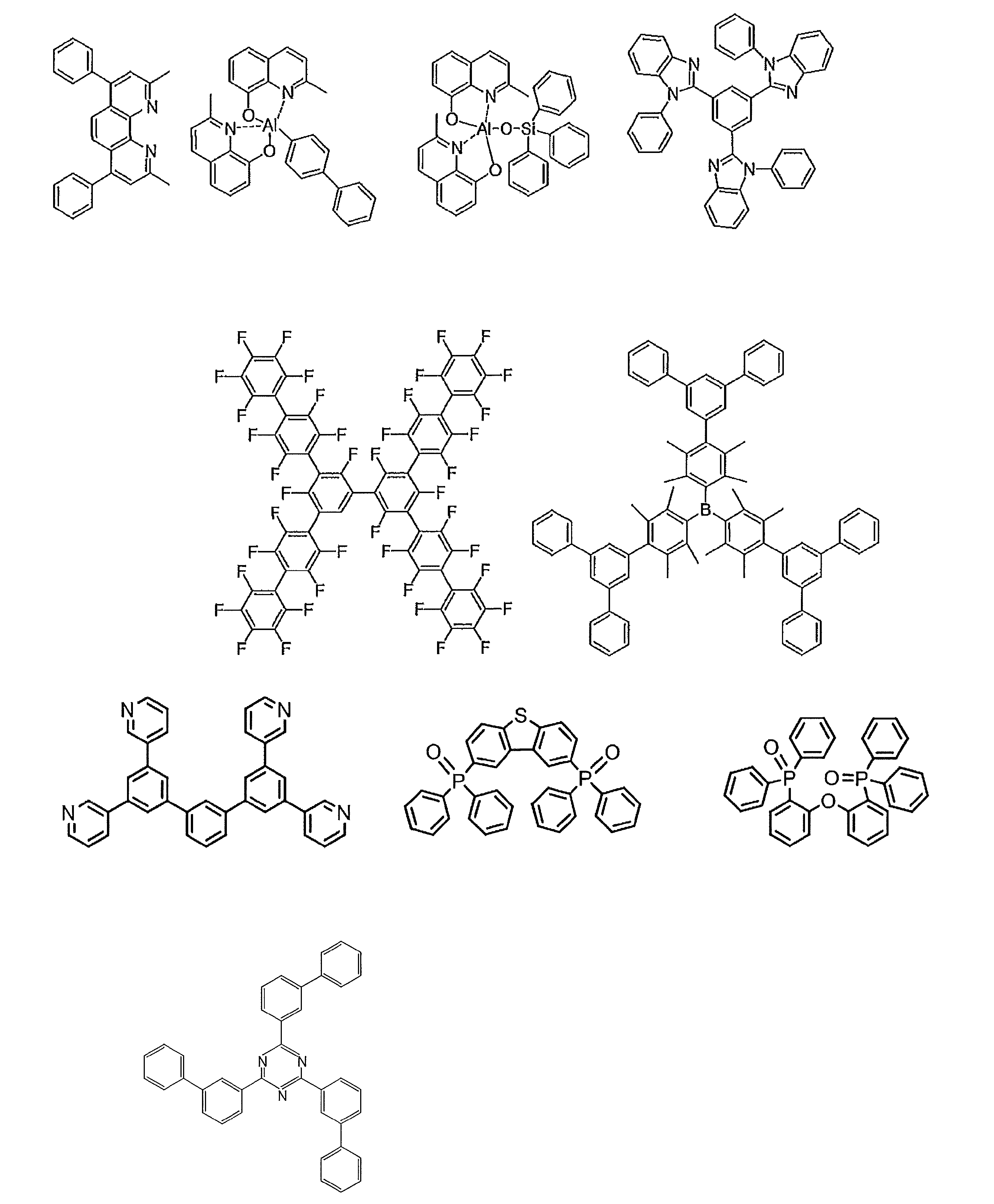
次に、電子輸送材料として用いることができる好ましい化合物例を挙げる。

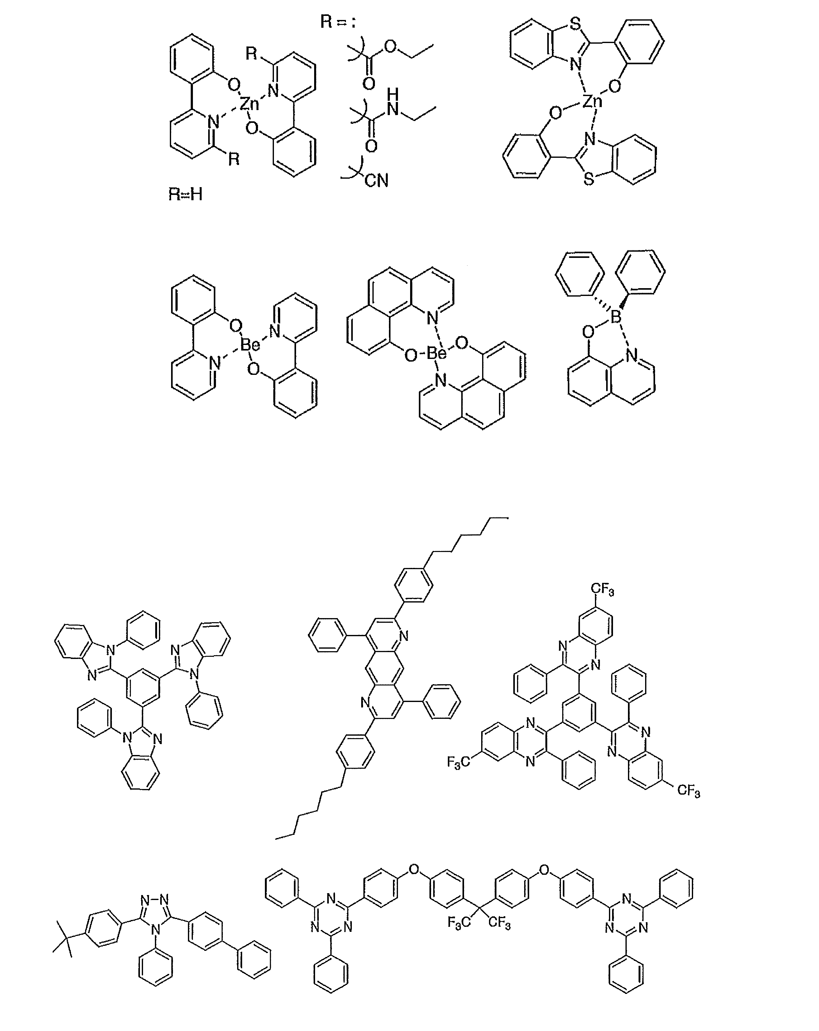

次に、電子注入材料として用いることができる好ましい化合物例を挙げる。
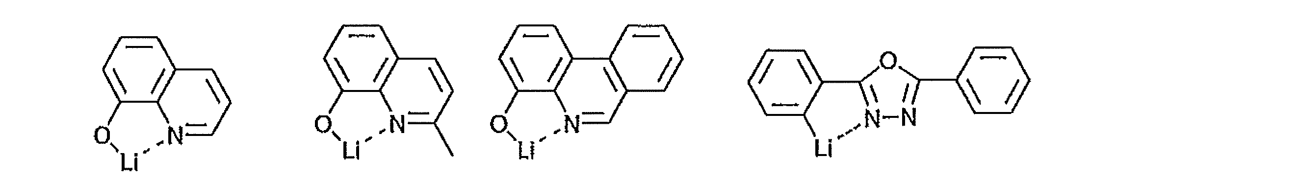
さらに添加可能な材料として好ましい化合物例を挙げる。例えば、安定化材料として添加すること等が考えられる。
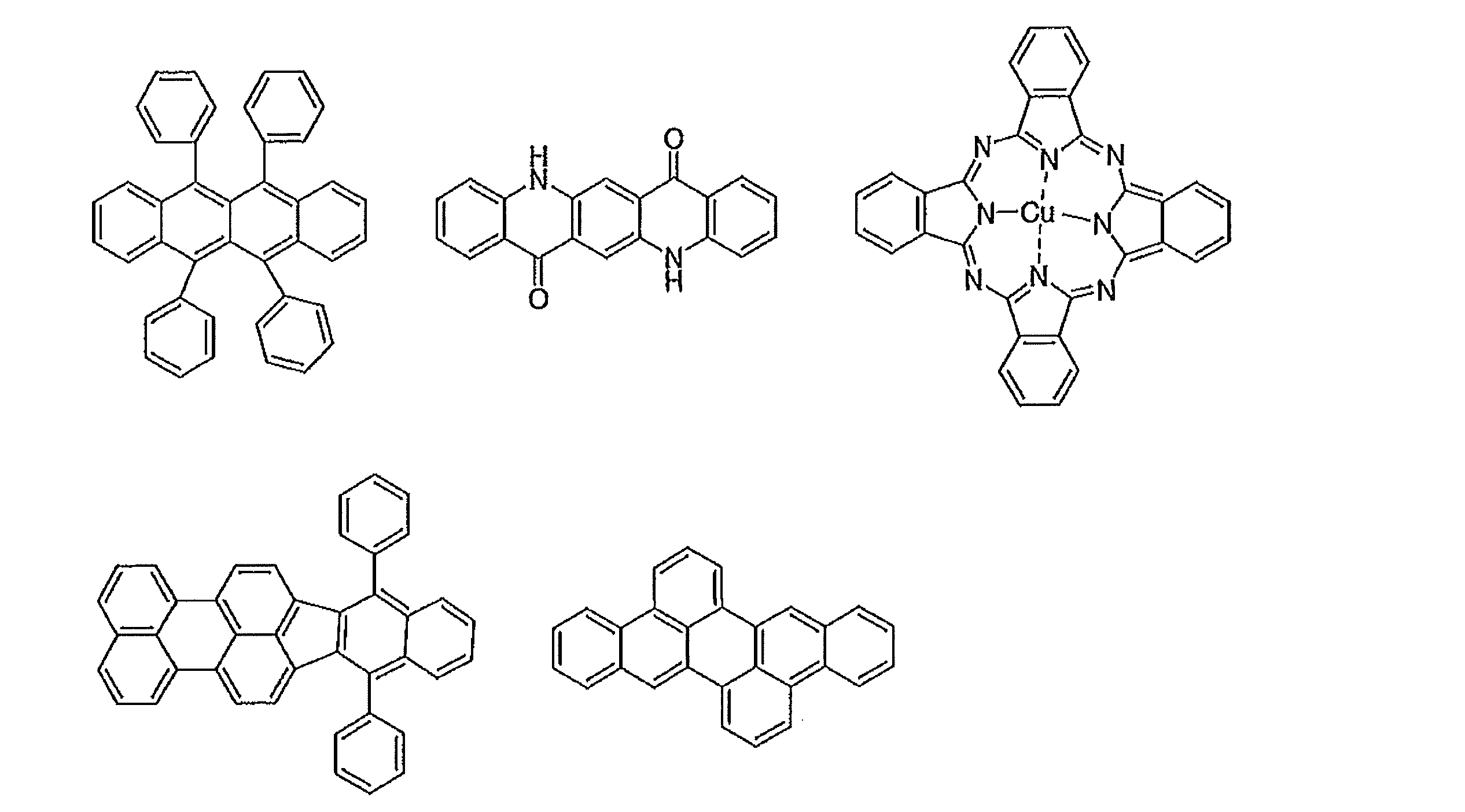
上述の方法により作製された有機エレクトロルミネッセンス素子は、得られた素子の陽極と陰極の間に電界を印加することにより発光する。このとき、励起一重項エネルギーによる発光であれば、そのエネルギーレベルに応じた波長の光が、蛍光発光および遅延蛍光発光として確認される。また、励起三重項エネルギーによる発光であれば、そのエネルギーレベルに応じた波長が、りん光として確認される。通常の蛍光は、遅延蛍光発光よりも蛍光寿命が短いため、発光寿命は蛍光と遅延蛍光で区別できる。
一方、りん光については、本発明の化合物のような通常の有機化合物では、励起三重項エネルギーは不安定で熱等に変換され、寿命が短く直ちに失活するため、室温では殆ど観測できない。通常の有機化合物の励起三重項エネルギーを測定するためには、極低温の条件での発光を観測することにより測定可能である。
一方、りん光については、本発明の化合物のような通常の有機化合物では、励起三重項エネルギーは不安定で熱等に変換され、寿命が短く直ちに失活するため、室温では殆ど観測できない。通常の有機化合物の励起三重項エネルギーを測定するためには、極低温の条件での発光を観測することにより測定可能である。
本発明の有機エレクトロルミネッセンス素子は、単一の素子、アレイ状に配置された構造からなる素子、陽極と陰極がX-Yマトリックス状に配置された構造のいずれにおいても適用することができる。本発明によれば、発光層に一般式(1)で表される化合物を含有させることにより、発光効率が大きく改善された有機発光素子が得られる。本発明の有機エレクトロルミネッセンス素子などの有機発光素子は、さらに様々な用途へ応用することが可能である。例えば、本発明の有機エレクトロルミネッセンス素子を用いて、有機エレクトロルミネッセンス表示装置を製造することが可能であり、詳細については、時任静士、安達千波矢、村田英幸共著「有機ELディスプレイ」(オーム社)を参照することができる。また、特に本発明の有機エレクトロルミネッセンス素子は、需要が大きい有機エレクトロルミネッセンス照明やバックライトに応用することもできる。
以下に合成例および実施例を挙げて本発明の特徴をさらに具体的に説明する。以下に示す材料、処理内容、処理手順等は、本発明の趣旨を逸脱しない限り適宜変更することができる。したがって、本発明の範囲は以下に示す具体例により限定的に解釈されるべきものではない。
(合成例1) 化合物1の合成
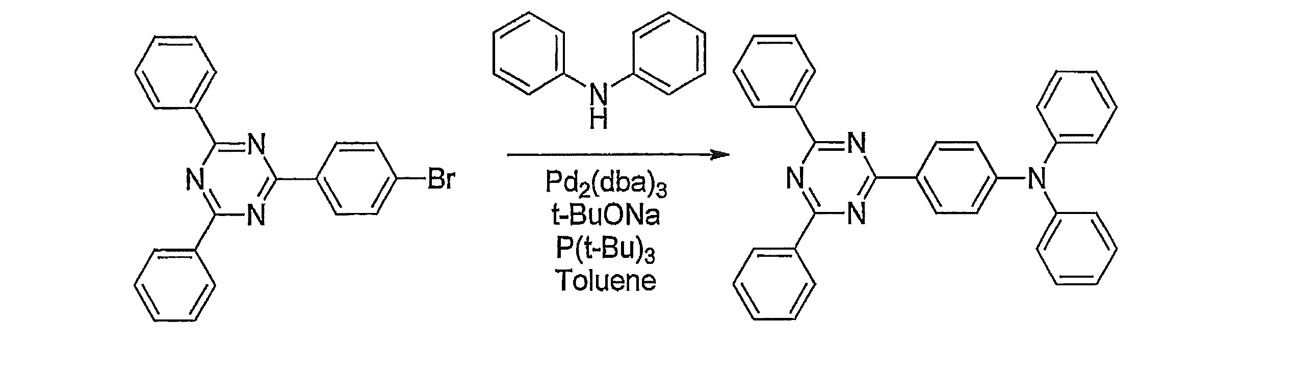
2-(4-ブロモフェニル)-4,6-ジフェニルトリアジン2.00g(5.15mmol)、ナトリウム tert-ブトキシド0.594g(6.18mmol)、ジフェニルアミン1.31g(7.73mmol)、トリス(ジベンジリデンアセトン)ジパラジウム(0)99.7mg(0.109mmol)を100mL三つ口フラスコに入れ、フラスコ内を窒素置換した。この混合物へトルエン30mL、0.75mol/L濃度のトリ(tert-ブチル)ホスフィンのトルエン溶液1.0mLを加えた。この混合物を30分間窒素バブリングした後、窒素雰囲気下、80℃で20時間攪拌した。攪拌後、この混合物をセライト、シリカゲルを通して吸引ろ過してろ液を得た。得られたろ液に水を加えて洗浄した。洗浄後、有機層と水層を分離し、有機層に硫酸マグネシウムを加えて乾燥した。乾燥後、この混合物を吸引ろ過してろ液を得た。得られたろ液を濃縮して得た固体をアセトンとメタノールの混合溶媒で洗浄したところ、化合物1を収量2.40g、収率97.8%で得た。図2に1H-NMRスペクトル(CDCl3,500MHz)を示す。

4-(4,6-ジフェニル-1,3,5-トリアジン-2-イル)トリフェニルアミン2.40g(5.03mmol)、テトラヒドロフラン20mL、酢酸エチル20mLを100mLエーレンマイヤーフラスコに入れて攪拌した。この溶液を0℃に冷却した後、N-ブロモこはく酸イミド2.08g(11.7mmol)を少量ずつ加えた。この溶液を室温で24時間攪拌したところ、固体が析出した。攪拌後、この混合物に水を加えて攪拌した。攪拌後、この混合物の有機層を濃縮し、水100mLを加えて攪拌した後、吸引ろ過して固体を得た。得られた固体をアセトンとメタノールの混合溶媒で洗浄したところ、目的物の粉末状淡黄色固体を収量2.97g、収率93.1%得た。

4,4’-ジブロモ-4’’-(4,6-ジフェニル-1,3,5-トリアジン-2-イル)トリフェニルアミン1.50g(2.36mmol)、ジフェニルアミン1.00g(5.91mmol)、トリス(ジベンジリデンアセトン)ジパラジウム(0)43.2mg(0.0472mmol)、ナトリウム tert-ブトキシド0.681g(7.09mmol)を100mL三つ口フラスコに入れ、フラスコ内を窒素置換した。この混合物へ、トルエン20mL、0.75mol/L濃度のトリ(tert-ブチル)ホスフィンのトルエン溶液1.0mLを加えた。この混合物を窒素雰囲気下、80℃で20時間攪拌した。攪拌後、この混合物を水100mL、トルエン100mLに加えて攪拌した。攪拌後、この混合物の水層を除去し、セライト、シリカゲルを通して吸引ろ過した。得られたろ液に水を加えて洗浄した。洗浄後、有機層と水層を分離し、有機層に硫酸マグネシウムを加えて乾燥した。乾燥後、この混合物を吸引ろ過してろ液を得た。得られたろ液を濃縮して得た固体をアセトンとメタノールの混合溶媒で洗浄したところ、粉末状黄色固体の化合物1を収量1.71g、収量89.3%で得た。
1H NMR(500MHz,CDCl3):δ8.75(d,J=8.5Hz,4H),8.62,(d,J=9.0Hz,2H),7.61-7.53(m,6H),7.29-7.26(m,8H),7.17-7.05(m,22H).
1H NMR(500MHz,CDCl3):δ8.75(d,J=8.5Hz,4H),8.62,(d,J=9.0Hz,2H),7.61-7.53(m,6H),7.29-7.26(m,8H),7.17-7.05(m,22H).
(実施例1) 有機フォトルミネッセンス素子の作製と評価(溶液)
合成例1で合成した化合物1のトルエン溶液(濃度10-5mol/L)を調製して、窒素をバブリングしながら300Kで紫外光を照射したところ、図3に示すようにピーク波長が565nmの蛍光が観測された。化合物1のトルエン溶液中でのフォトルミネッセンス量子効率を絶対PL量子収率測定装置(浜松ホトニクス(株)製Quantaurus-QY)により300Kで測定したところ、窒素バブル前が34.8%で窒素バブル後が44.5%となり、約10%の増加が見られた。図4に窒素バブル後の過渡減衰曲線を示す。この過渡減衰曲線は、化合物に励起光を当てて発光強度が失活してゆく過程を測定した発光寿命測定結果を示すものである。通常の一成分の発光(蛍光もしくはリン光)では発光強度は単一指数関数的に減衰する。これは、グラフの縦軸がセミlog である場合には、直線的に減衰することを意味している。化合物1の過渡減衰曲線では、観測初期にこのような直線的成分(蛍光)が観測されているが、それ以降は直線性から外れる成分が現れている。これは遅延成分の発光であり、初期の成分と加算される信号は、長時間側に裾をひくゆるい曲線になる。このように発光寿命を測定することによって、化合物1は蛍光成分のほかに遅延成分を含む発光体であることが確認された。
合成例1で合成した化合物1のトルエン溶液(濃度10-5mol/L)を調製して、窒素をバブリングしながら300Kで紫外光を照射したところ、図3に示すようにピーク波長が565nmの蛍光が観測された。化合物1のトルエン溶液中でのフォトルミネッセンス量子効率を絶対PL量子収率測定装置(浜松ホトニクス(株)製Quantaurus-QY)により300Kで測定したところ、窒素バブル前が34.8%で窒素バブル後が44.5%となり、約10%の増加が見られた。図4に窒素バブル後の過渡減衰曲線を示す。この過渡減衰曲線は、化合物に励起光を当てて発光強度が失活してゆく過程を測定した発光寿命測定結果を示すものである。通常の一成分の発光(蛍光もしくはリン光)では発光強度は単一指数関数的に減衰する。これは、グラフの縦軸がセミlog である場合には、直線的に減衰することを意味している。化合物1の過渡減衰曲線では、観測初期にこのような直線的成分(蛍光)が観測されているが、それ以降は直線性から外れる成分が現れている。これは遅延成分の発光であり、初期の成分と加算される信号は、長時間側に裾をひくゆるい曲線になる。このように発光寿命を測定することによって、化合物1は蛍光成分のほかに遅延成分を含む発光体であることが確認された。
(比較例1) 有機フォトルミネッセンス素子の作製と評価(溶液)
化合物1のかわりに、比較化合物として上記の化合物Aを用いて、実施例1と同様にトルエン溶液を調製した。図5に発光スペクトルを示し、図6に過渡減衰曲線を示す。窒素バブル前後で差が見られず、遅延蛍光は確認されなかった。
化合物1のかわりに、比較化合物として上記の化合物Aを用いて、実施例1と同様にトルエン溶液を調製した。図5に発光スペクトルを示し、図6に過渡減衰曲線を示す。窒素バブル前後で差が見られず、遅延蛍光は確認されなかった。
(実施例2) 有機フォトルミネッセンス素子の作製と評価(薄膜)
シリコン基板上に真空蒸着法にて、真空度5.0×10⁻⁴Paの条件にて化合物1とmCBPとを異なる蒸着源から蒸着し、化合物1の濃度が6.0重量%である薄膜を0.3nm/秒にて100nmの厚さで形成して有機フォトルミネッセンス素子とした。実施例1と同じ測定装置を用いて得た発光スペクトルを図7に示す(ピーク波長539nm)。また、300K、250K、200K、150Kにおいて小型蛍光寿命測定装置(浜松ホトニクス(株)製Quantaurus-tau)による測定を行って、図8に示す過渡減衰曲線を得た。図8より、温度低下に伴って遅延蛍光成分が減少する熱活性型の遅延蛍光であることが確認された。フォトルミネッセンス量子効率は窒素流通下で300Kにて100%であった。
シリコン基板上に真空蒸着法にて、真空度5.0×10⁻⁴Paの条件にて化合物1とmCBPとを異なる蒸着源から蒸着し、化合物1の濃度が6.0重量%である薄膜を0.3nm/秒にて100nmの厚さで形成して有機フォトルミネッセンス素子とした。実施例1と同じ測定装置を用いて得た発光スペクトルを図7に示す(ピーク波長539nm)。また、300K、250K、200K、150Kにおいて小型蛍光寿命測定装置(浜松ホトニクス(株)製Quantaurus-tau)による測定を行って、図8に示す過渡減衰曲線を得た。図8より、温度低下に伴って遅延蛍光成分が減少する熱活性型の遅延蛍光であることが確認された。フォトルミネッセンス量子効率は窒素流通下で300Kにて100%であった。
(実施例3) 有機エレクトロルミネッセンス素子の作製と評価
膜厚100nmのインジウム・スズ酸化物(ITO)からなる陽極が形成されたガラス基板上に、各薄膜を真空蒸着法にて、真空度5.0×10⁻⁴Paで積層した。まず、ITO上にα-NPDを35nmの厚さに形成した。次に、化合物1とmCBPを異なる蒸着源から共蒸着し、15nmの厚さの層を形成して発光層とした。この時、化合物1の濃度は6.0重量%とした。次に、TPBiを65nmの厚さに形成し、さらにフッ化リチウム(LiF)を0.8nm真空蒸着し、次いでアルミニウム(Al)を100nmの厚さに蒸着することにより陰極を形成し、有機エレクトロルミネッセンス素子とした。
製造した有機エレクトロルミネッセンス素子を、半導体パラメータ・アナライザ(アジレント・テクノロジー社製:E5273A)、光パワーメータ測定装置(ニューポート社製:1930C)、および光学分光器(オーシャンオプティクス社製:USB2000)を用いて測定したところ、図9に示すように548nmの発光が認められた。電圧-電流密度特性を図10に示し、電流密度-外部量子効率特性を図11に示す。化合物1を発光材料として用いた有機エレクトロルミネッセンス素子は15.44%の高い外部量子効率を達成した。仮に発光量子効率が100%の蛍光材料を用いてバランスの取れた理想的な有機エレクトロルミネッセンス素子を試作したとすると、光取り出し効率が20~30%であれば、蛍光発光の外部量子効率は5~7.5%となる。この値が一般に、蛍光材料を用いた有機エレクトロルミネッセンス素子の外部量子効率の理論限界値とされている。化合物1を用いた本発明の有機エレクトロルミネッセンス素子は、理論限界値を超える高い外部量子効率を実現している点で極めて優れている。
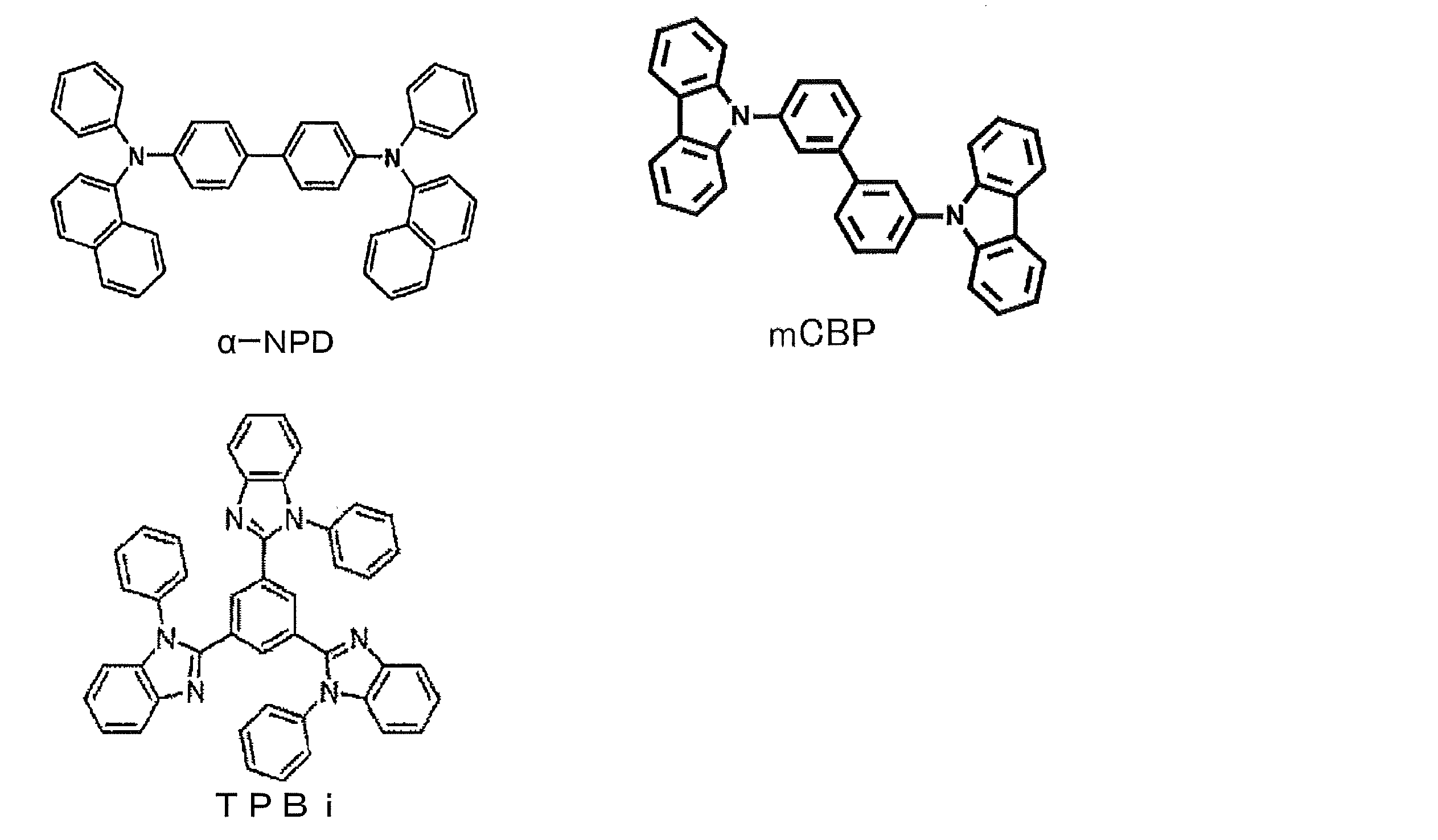
本発明の化合物は発光材料として有用である。このため本発明の化合物は、有機エレクトロルミネッセンス素子などの有機発光素子用の発光材料として効果的に用いられる。本発明の化合物の中には、遅延蛍光が放射するものも含まれているため、発光効率が高い有機発光素子を提供することも可能である。このため、本発明は産業上の利用可能性が高い。
1 基板
2 陽極
3 正孔注入層
4 正孔輸送層
5 発光層
6 電子輸送層
7 陰極
2 陽極
3 正孔注入層
4 正孔輸送層
5 発光層
6 電子輸送層
7 陰極
Claims (15)
- 下記一般式(1)で表される化合物。
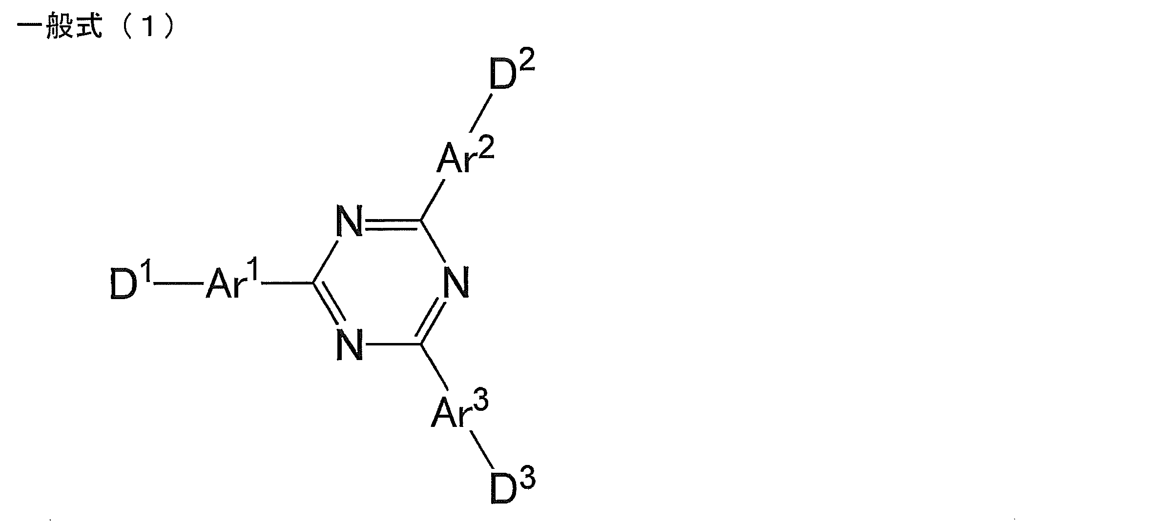

- 一般式(1)のD1、D2およびD3の少なくとも1つが、前記群1-1から選択される構造を有する基でメタ位またはパラ位が置換されたジフェニルアミノ基を表すことを特徴とする請求項1に記載の化合物。
- 一般式(1)のD1、D2およびD3の少なくとも1つが、下記の群1-2:


- 一般式(1)のD1、D2およびD3の少なくとも1つが、下記の群1-3:

- 一般式(1)のAr1、Ar2およびAr3が、各々独立に置換もしくは無置換のフェニレン基、置換もしくは無置換のピリジレン基、またはこれらのいずれか2つが連結した連結基であることを特徴とする請求項1~4のいずれか1項に記載の化合物。
- 一般式(1)のAr1、Ar2およびAr3が、各々独立に下記の群2-1:

- 一般式(1)のD1が前記の群1-1から選択される基で置換されたジアリールアミノ基であって、Ar1が置換もしくは無置換のパラフェニレン基であることを特徴とする請求項1~6のいずれか1項に記載の化合物。
- 下記一般式(2)で表される構造を有する請求項1に記載の化合物。
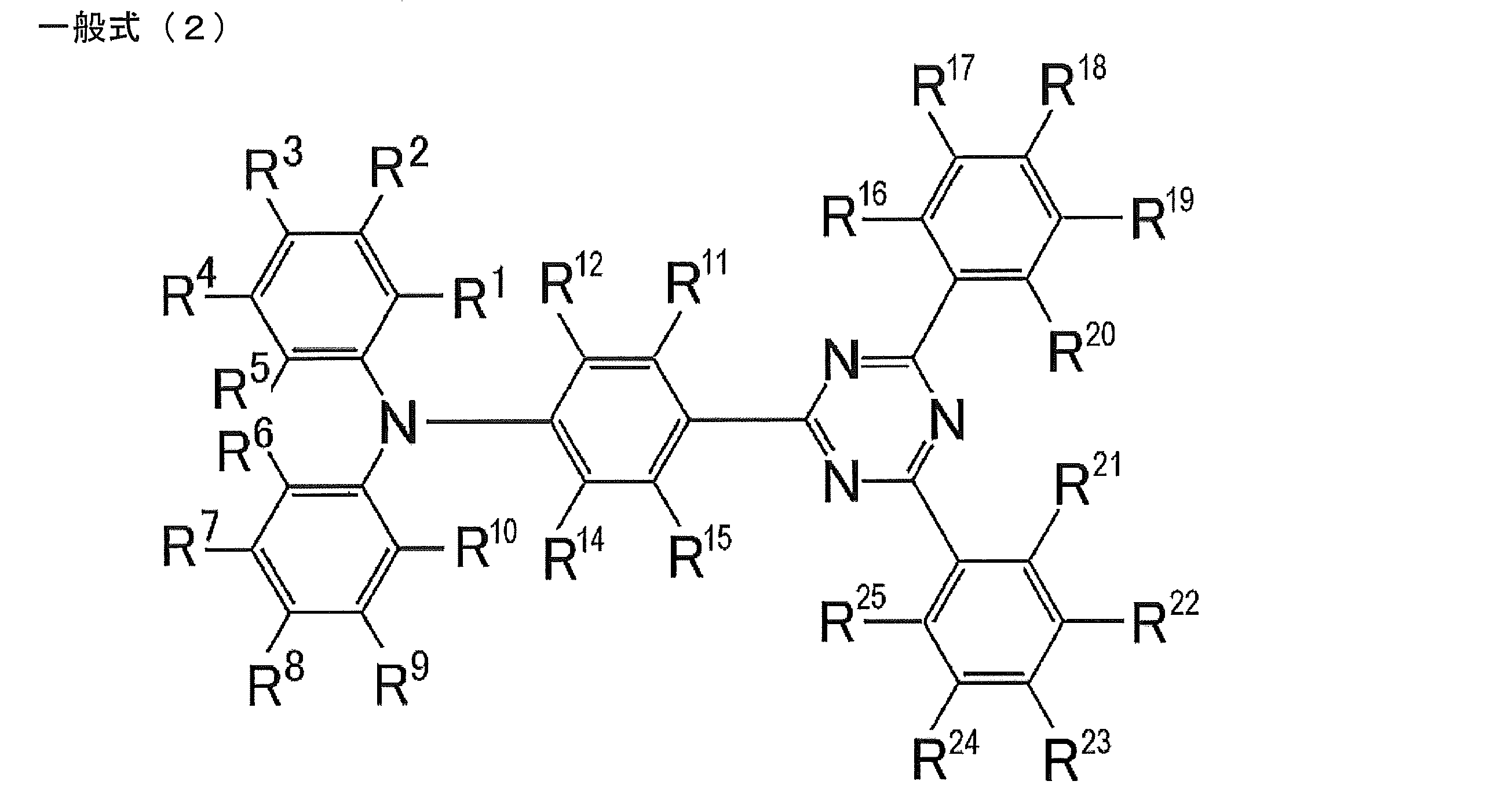

- R1~R12およびR14~R25のうちの少なくとも1つが前記群1-1から選択される基で置換されたジアリールアミノ基を表し、その他のR1~R12およびR14~R25が水素原子であることを特徴とする請求項8に記載の化合物。
- R2、R3、R7、R8のうちの少なくとも1つが、前記群1-1から選択される基で置換されたジアリールアミノ基を表すことを特徴とする請求項8または9に記載の化合物。
- 請求項1~10のいずれか1項に記載の化合物からなる発光材料。
- 請求項1~10のいずれか1項に記載の化合物からなる遅延蛍光体。
- 請求項11に記載の発光材料を含む発光層を基板上に有することを特徴とする有機発光素子。
- 遅延蛍光を放射することを特徴とする請求項13に記載の有機発光素子。
- 有機エレクトロルミネッセンス素子であることを特徴とする請求項13または14に記載の有機発光素子。
Applications Claiming Priority (2)
| Application Number | Priority Date | Filing Date | Title |
|---|---|---|---|
| JP2013-046229 | 2013-03-08 | ||
| JP2013046229A JP6293417B2 (ja) | 2013-03-08 | 2013-03-08 | 化合物、発光材料および有機発光素子 |
Publications (1)
| Publication Number | Publication Date |
|---|---|
| WO2014136860A1 true WO2014136860A1 (ja) | 2014-09-12 |
Family
ID=51491368
Family Applications (1)
| Application Number | Title | Priority Date | Filing Date |
|---|---|---|---|
| PCT/JP2014/055720 WO2014136860A1 (ja) | 2013-03-08 | 2014-03-06 | 化合物、発光材料および有機発光素子 |
Country Status (3)
| Country | Link |
|---|---|
| JP (1) | JP6293417B2 (ja) |
| TW (1) | TW201443028A (ja) |
| WO (1) | WO2014136860A1 (ja) |
Cited By (18)
| Publication number | Priority date | Publication date | Assignee | Title |
|---|---|---|---|---|
| WO2016052819A1 (ko) * | 2014-10-01 | 2016-04-07 | 가톨릭대학교 산학협력단 | 유기 광전자 소자용 화합물 및 이를 포함하는 유기 광전자 소자 |
| CN106279115A (zh) * | 2015-06-10 | 2017-01-04 | 上海和辉光电有限公司 | 一种用于发光材料的化合物 |
| WO2020076796A1 (en) | 2018-10-09 | 2020-04-16 | Kyulux, Inc. | Novel composition of matter for use in organic light-emitting diodes |
| WO2021157642A1 (ja) | 2020-02-04 | 2021-08-12 | 株式会社Kyulux | ホスト材料、組成物および有機発光素子 |
| US11101440B2 (en) | 2015-07-01 | 2021-08-24 | Kyushu University, National University Corporation | Organic electroluminescent device |
| WO2021235549A1 (ja) | 2020-05-22 | 2021-11-25 | 株式会社Kyulux | 化合物、発光材料および発光素子 |
| CN113793905A (zh) * | 2014-09-26 | 2021-12-14 | Udc 爱尔兰有限责任公司 | 具有高效率的荧光有机发光元件 |
| WO2022025248A1 (ja) | 2020-07-31 | 2022-02-03 | 株式会社Kyulux | 化合物、発光材料および発光素子 |
| US11335872B2 (en) | 2016-09-06 | 2022-05-17 | Kyulux, Inc. | Organic light-emitting device |
| WO2022168956A1 (ja) | 2021-02-04 | 2022-08-11 | 株式会社Kyulux | 化合物、発光材料および有機発光素子 |
| US11476435B2 (en) | 2017-08-24 | 2022-10-18 | Kyushu University, National University Corporation | Film and organic light-emitting device containing perovskite-type compound and organic light-emitting material |
| US11482679B2 (en) | 2017-05-23 | 2022-10-25 | Kyushu University, National University Corporation | Compound, light-emitting lifetime lengthening agent, use of n-type compound, film and light-emitting device |
| WO2022244503A1 (ja) | 2021-05-20 | 2022-11-24 | 株式会社Kyulux | 有機発光素子 |
| WO2022270602A1 (ja) | 2021-06-23 | 2022-12-29 | 株式会社Kyulux | 有機発光素子および膜 |
| WO2022270354A1 (ja) | 2021-06-23 | 2022-12-29 | 株式会社Kyulux | 化合物、発光材料および有機発光素子 |
| WO2023282224A1 (ja) | 2021-07-06 | 2023-01-12 | 株式会社Kyulux | 有機発光素子およびその設計方法 |
| WO2023053835A1 (ja) | 2021-09-28 | 2023-04-06 | 株式会社Kyulux | 化合物、組成物、ホスト材料、電子障壁材料および有機発光素子 |
| US11930654B2 (en) | 2017-07-06 | 2024-03-12 | Kyulux, Inc. | Organic light-emitting element |
Families Citing this family (3)
| Publication number | Priority date | Publication date | Assignee | Title |
|---|---|---|---|---|
| CN106892857B (zh) | 2015-12-18 | 2020-02-18 | 昆山国显光电有限公司 | 热活化延迟荧光材料及其在有机电致发光器件中的应用 |
| CN105399696B (zh) * | 2015-12-25 | 2019-12-24 | 上海天马有机发光显示技术有限公司 | 有机电致发光化合物及其有机光电装置 |
| JP6770900B2 (ja) * | 2017-01-12 | 2020-10-21 | 日本放送協会 | 有機エレクトロルミネッセンス素子 |
Citations (6)
| Publication number | Priority date | Publication date | Assignee | Title |
|---|---|---|---|---|
| JPH11292860A (ja) * | 1998-04-02 | 1999-10-26 | Mitsubishi Chemical Corp | トリアミン系化合物及びその製造方法 |
| JP2002193952A (ja) * | 2000-12-25 | 2002-07-10 | Fuji Photo Film Co Ltd | 新規含窒素へテロ環化合物、発光素子材料およびそれらを使用した発光素子 |
| JP2005183303A (ja) * | 2003-12-22 | 2005-07-07 | Fuji Photo Film Co Ltd | 有機電界発光素子 |
| JP2012500789A (ja) * | 2008-08-22 | 2012-01-12 | エルジー・ケム・リミテッド | 有機電子素子材料およびこれを用いた有機電子素子 |
| WO2012015274A2 (ko) * | 2010-07-30 | 2012-02-02 | 롬엔드하스전재재로코리아유한회사 | 유기발광화합물을 발광재료로서 채용하고 있는 유기 전계 발광 소자 |
| WO2013081088A1 (ja) * | 2011-12-02 | 2013-06-06 | 国立大学法人九州大学 | 有機発光素子ならびにそれに用いる遅延蛍光材料および化合物 |
-
2013
- 2013-03-08 JP JP2013046229A patent/JP6293417B2/ja active Active
-
2014
- 2014-03-06 WO PCT/JP2014/055720 patent/WO2014136860A1/ja active Application Filing
- 2014-03-06 TW TW103107726A patent/TW201443028A/zh unknown
Patent Citations (6)
| Publication number | Priority date | Publication date | Assignee | Title |
|---|---|---|---|---|
| JPH11292860A (ja) * | 1998-04-02 | 1999-10-26 | Mitsubishi Chemical Corp | トリアミン系化合物及びその製造方法 |
| JP2002193952A (ja) * | 2000-12-25 | 2002-07-10 | Fuji Photo Film Co Ltd | 新規含窒素へテロ環化合物、発光素子材料およびそれらを使用した発光素子 |
| JP2005183303A (ja) * | 2003-12-22 | 2005-07-07 | Fuji Photo Film Co Ltd | 有機電界発光素子 |
| JP2012500789A (ja) * | 2008-08-22 | 2012-01-12 | エルジー・ケム・リミテッド | 有機電子素子材料およびこれを用いた有機電子素子 |
| WO2012015274A2 (ko) * | 2010-07-30 | 2012-02-02 | 롬엔드하스전재재로코리아유한회사 | 유기발광화합물을 발광재료로서 채용하고 있는 유기 전계 발광 소자 |
| WO2013081088A1 (ja) * | 2011-12-02 | 2013-06-06 | 国立大学法人九州大学 | 有機発光素子ならびにそれに用いる遅延蛍光材料および化合物 |
Non-Patent Citations (2)
| Title |
|---|
| HIROYUKI TANAKA ET AL.: "Efficient green thermally activated delayed fluorescence (TADF) from a phenoxazine-triphenyltriazine (PXZ-TRZ) derivative", CHEM. COMMUN., vol. 48, 2012, pages 11392 - 11394 * |
| SAE YOUN LEE ET AL.: "High-efficiency organic light-emitting diodes utilizing thermally activated delayed fluorescence from triazine- based donor-acceptor hybrid molecules", APPL. PHYS. LETT., vol. 101, August 2012 (2012-08-01), pages 093306 - 093306-4 * |
Cited By (19)
| Publication number | Priority date | Publication date | Assignee | Title |
|---|---|---|---|---|
| CN113793905A (zh) * | 2014-09-26 | 2021-12-14 | Udc 爱尔兰有限责任公司 | 具有高效率的荧光有机发光元件 |
| WO2016052819A1 (ko) * | 2014-10-01 | 2016-04-07 | 가톨릭대학교 산학협력단 | 유기 광전자 소자용 화합물 및 이를 포함하는 유기 광전자 소자 |
| CN106279115A (zh) * | 2015-06-10 | 2017-01-04 | 上海和辉光电有限公司 | 一种用于发光材料的化合物 |
| US11101440B2 (en) | 2015-07-01 | 2021-08-24 | Kyushu University, National University Corporation | Organic electroluminescent device |
| US11335872B2 (en) | 2016-09-06 | 2022-05-17 | Kyulux, Inc. | Organic light-emitting device |
| US11482679B2 (en) | 2017-05-23 | 2022-10-25 | Kyushu University, National University Corporation | Compound, light-emitting lifetime lengthening agent, use of n-type compound, film and light-emitting device |
| US11930654B2 (en) | 2017-07-06 | 2024-03-12 | Kyulux, Inc. | Organic light-emitting element |
| US11476435B2 (en) | 2017-08-24 | 2022-10-18 | Kyushu University, National University Corporation | Film and organic light-emitting device containing perovskite-type compound and organic light-emitting material |
| WO2020076796A1 (en) | 2018-10-09 | 2020-04-16 | Kyulux, Inc. | Novel composition of matter for use in organic light-emitting diodes |
| WO2021157593A1 (ja) | 2020-02-04 | 2021-08-12 | 株式会社Kyulux | 組成物、膜、有機発光素子、発光組成物を提供する方法およびプログラム |
| WO2021157642A1 (ja) | 2020-02-04 | 2021-08-12 | 株式会社Kyulux | ホスト材料、組成物および有機発光素子 |
| WO2021235549A1 (ja) | 2020-05-22 | 2021-11-25 | 株式会社Kyulux | 化合物、発光材料および発光素子 |
| WO2022025248A1 (ja) | 2020-07-31 | 2022-02-03 | 株式会社Kyulux | 化合物、発光材料および発光素子 |
| WO2022168956A1 (ja) | 2021-02-04 | 2022-08-11 | 株式会社Kyulux | 化合物、発光材料および有機発光素子 |
| WO2022244503A1 (ja) | 2021-05-20 | 2022-11-24 | 株式会社Kyulux | 有機発光素子 |
| WO2022270602A1 (ja) | 2021-06-23 | 2022-12-29 | 株式会社Kyulux | 有機発光素子および膜 |
| WO2022270354A1 (ja) | 2021-06-23 | 2022-12-29 | 株式会社Kyulux | 化合物、発光材料および有機発光素子 |
| WO2023282224A1 (ja) | 2021-07-06 | 2023-01-12 | 株式会社Kyulux | 有機発光素子およびその設計方法 |
| WO2023053835A1 (ja) | 2021-09-28 | 2023-04-06 | 株式会社Kyulux | 化合物、組成物、ホスト材料、電子障壁材料および有機発光素子 |
Also Published As
| Publication number | Publication date |
|---|---|
| TW201443028A (zh) | 2014-11-16 |
| JP2014172852A (ja) | 2014-09-22 |
| JP6293417B2 (ja) | 2018-03-14 |
Similar Documents
| Publication | Publication Date | Title |
|---|---|---|
| JP6293417B2 (ja) | 化合物、発光材料および有機発光素子 | |
| JP6262711B2 (ja) | 化合物、発光材料および有機発光素子 | |
| JP6225111B2 (ja) | 発光材料、化合物、およびそれらを用いた有機発光素子 | |
| KR102076887B1 (ko) | 발광 재료, 유기 발광 소자 및 화합물 | |
| JP6263524B2 (ja) | 化合物、発光材料および有機発光素子 | |
| JP5594750B2 (ja) | 化合物、発光材料および有機発光素子 | |
| JP6472383B2 (ja) | 発光材料、並びに、これを用いた遅延蛍光体および有機発光素子 | |
| JP6277182B2 (ja) | 化合物、発光材料および有機発光素子 | |
| JP6367189B2 (ja) | 発光材料、有機発光素子および化合物 | |
| JP6383538B2 (ja) | 発光材料、有機発光素子および化合物 | |
| JP6326050B2 (ja) | 化合物、発光材料および有機発光素子 | |
| JP6466913B2 (ja) | 発光材料、有機発光素子および化合物 | |
| WO2015080183A1 (ja) | 発光材料、有機発光素子および化合物 | |
| WO2015133501A1 (ja) | 発光材料、有機発光素子および化合物 | |
| WO2015108049A1 (ja) | 発光材料、有機発光素子および化合物 | |
| WO2013154064A1 (ja) | 有機発光素子ならびにそれに用いる発光材料および化合物 | |
| WO2013161437A1 (ja) | 発光材料および有機発光素子 | |
| JP6647514B2 (ja) | 有機発光素子ならびにそれに用いる発光材料および化合物 | |
| WO2014126076A1 (ja) | 化合物、発光材料および有機発光素子 | |
| JP2018111751A (ja) | 発光材料、化合物および有機発光素子 | |
| JP2016084283A (ja) | 化合物、発光材料および有機発光素子 | |
| JP2016084284A (ja) | 化合物、発光材料および有機発光素子 |
Legal Events
| Date | Code | Title | Description |
|---|---|---|---|
| 121 | Ep: the epo has been informed by wipo that ep was designated in this application |
Ref document number: 14760424 Country of ref document: EP Kind code of ref document: A1 |
|
| NENP | Non-entry into the national phase |
Ref country code: DE |
|
| 122 | Ep: pct application non-entry in european phase |
Ref document number: 14760424 Country of ref document: EP Kind code of ref document: A1 |