WO2014129506A1 - 光デバイス - Google Patents
光デバイス Download PDFInfo
- Publication number
- WO2014129506A1 WO2014129506A1 PCT/JP2014/053940 JP2014053940W WO2014129506A1 WO 2014129506 A1 WO2014129506 A1 WO 2014129506A1 JP 2014053940 W JP2014053940 W JP 2014053940W WO 2014129506 A1 WO2014129506 A1 WO 2014129506A1
- Authority
- WO
- WIPO (PCT)
- Prior art keywords
- light
- waveguide
- condensing
- substrate
- optical
- Prior art date
- Legal status (The legal status is an assumption and is not a legal conclusion. Google has not performed a legal analysis and makes no representation as to the accuracy of the status listed.)
- Ceased
Links
Images





Classifications
-
- G—PHYSICS
- G02—OPTICS
- G02B—OPTICAL ELEMENTS, SYSTEMS OR APPARATUS
- G02B6/00—Light guides; Structural details of arrangements comprising light guides and other optical elements, e.g. couplings
- G02B6/24—Coupling light guides
- G02B6/26—Optical coupling means
- G02B6/30—Optical coupling means for use between fibre and thin-film device
-
- G—PHYSICS
- G02—OPTICS
- G02B—OPTICAL ELEMENTS, SYSTEMS OR APPARATUS
- G02B6/00—Light guides; Structural details of arrangements comprising light guides and other optical elements, e.g. couplings
- G02B6/24—Coupling light guides
- G02B6/26—Optical coupling means
- G02B6/32—Optical coupling means having lens focusing means positioned between opposed fibre ends
- G02B6/327—Optical coupling means having lens focusing means positioned between opposed fibre ends with angled interfaces to reduce reflections
-
- G—PHYSICS
- G02—OPTICS
- G02B—OPTICAL ELEMENTS, SYSTEMS OR APPARATUS
- G02B6/00—Light guides; Structural details of arrangements comprising light guides and other optical elements, e.g. couplings
- G02B6/10—Light guides; Structural details of arrangements comprising light guides and other optical elements, e.g. couplings of the optical waveguide type
- G02B6/12—Light guides; Structural details of arrangements comprising light guides and other optical elements, e.g. couplings of the optical waveguide type of the integrated circuit kind
- G02B2006/12133—Functions
- G02B2006/12147—Coupler
-
- G—PHYSICS
- G02—OPTICS
- G02B—OPTICAL ELEMENTS, SYSTEMS OR APPARATUS
- G02B6/00—Light guides; Structural details of arrangements comprising light guides and other optical elements, e.g. couplings
- G02B6/10—Light guides; Structural details of arrangements comprising light guides and other optical elements, e.g. couplings of the optical waveguide type
- G02B6/12—Light guides; Structural details of arrangements comprising light guides and other optical elements, e.g. couplings of the optical waveguide type of the integrated circuit kind
- G02B6/122—Basic optical elements, e.g. light-guiding paths
-
- G—PHYSICS
- G02—OPTICS
- G02B—OPTICAL ELEMENTS, SYSTEMS OR APPARATUS
- G02B6/00—Light guides; Structural details of arrangements comprising light guides and other optical elements, e.g. couplings
- G02B6/24—Coupling light guides
- G02B6/42—Coupling light guides with opto-electronic elements
- G02B6/4201—Packages, e.g. shape, construction, internal or external details
- G02B6/4204—Packages, e.g. shape, construction, internal or external details the coupling comprising intermediate optical elements, e.g. lenses, holograms
- G02B6/4207—Packages, e.g. shape, construction, internal or external details the coupling comprising intermediate optical elements, e.g. lenses, holograms with optical elements reducing the sensitivity to optical feedback
- G02B6/4208—Packages, e.g. shape, construction, internal or external details the coupling comprising intermediate optical elements, e.g. lenses, holograms with optical elements reducing the sensitivity to optical feedback using non-reciprocal elements or birefringent plates, i.e. quasi-isolators
- G02B6/4209—Optical features
-
- G—PHYSICS
- G02—OPTICS
- G02F—OPTICAL DEVICES OR ARRANGEMENTS FOR THE CONTROL OF LIGHT BY MODIFICATION OF THE OPTICAL PROPERTIES OF THE MEDIA OF THE ELEMENTS INVOLVED THEREIN; NON-LINEAR OPTICS; FREQUENCY-CHANGING OF LIGHT; OPTICAL LOGIC ELEMENTS; OPTICAL ANALOGUE/DIGITAL CONVERTERS
- G02F1/00—Devices or arrangements for the control of the intensity, colour, phase, polarisation or direction of light arriving from an independent light source, e.g. switching, gating or modulating; Non-linear optics
- G02F1/01—Devices or arrangements for the control of the intensity, colour, phase, polarisation or direction of light arriving from an independent light source, e.g. switching, gating or modulating; Non-linear optics for the control of the intensity, phase, polarisation or colour
- G02F1/21—Devices or arrangements for the control of the intensity, colour, phase, polarisation or direction of light arriving from an independent light source, e.g. switching, gating or modulating; Non-linear optics for the control of the intensity, phase, polarisation or colour by interference
- G02F1/212—Mach-Zehnder type
-
- G—PHYSICS
- G02—OPTICS
- G02F—OPTICAL DEVICES OR ARRANGEMENTS FOR THE CONTROL OF LIGHT BY MODIFICATION OF THE OPTICAL PROPERTIES OF THE MEDIA OF THE ELEMENTS INVOLVED THEREIN; NON-LINEAR OPTICS; FREQUENCY-CHANGING OF LIGHT; OPTICAL LOGIC ELEMENTS; OPTICAL ANALOGUE/DIGITAL CONVERTERS
- G02F2201/00—Constructional arrangements not provided for in groups G02F1/00 - G02F7/00
- G02F2201/06—Constructional arrangements not provided for in groups G02F1/00 - G02F7/00 integrated waveguide
-
- G—PHYSICS
- G02—OPTICS
- G02F—OPTICAL DEVICES OR ARRANGEMENTS FOR THE CONTROL OF LIGHT BY MODIFICATION OF THE OPTICAL PROPERTIES OF THE MEDIA OF THE ELEMENTS INVOLVED THEREIN; NON-LINEAR OPTICS; FREQUENCY-CHANGING OF LIGHT; OPTICAL LOGIC ELEMENTS; OPTICAL ANALOGUE/DIGITAL CONVERTERS
- G02F2202/00—Materials and properties
- G02F2202/20—LiNbO3, LiTaO3
Definitions
- the present invention relates to an optical device.
- a polarization quadrature phase modulator As an optical device that enables high-speed and large-capacity optical fiber communication of 100 Gb / s, a polarization quadrature phase modulator (DP-QPSK) is known.
- DP-QPSK of Patent Document 1 two sets of Mach-Zehnder type optical waveguides are provided on an LN substrate, and one or both polarization planes of light emitted from each Mach-Zehnder type optical waveguide are rotated. These light beams are combined in such a manner that their polarization planes are orthogonal to each other, and are combined for output.
- the distance between the waveguides of the waveguides used in the modulator and the distance between the lenses of the lens array may include a manufacturing error derived from a mold, a photomask, or the like. Specifically, if it is considered that an error of about 1 ⁇ m occurs in each member as a manufacturing error, there is a possibility that a deviation of about 2 ⁇ m at maximum occurs if both manufacturing errors are taken into account. In this case, the coupling efficiency with the optical output unit for output from the modulator to the outside is lowered due to reasons such as deviation from the designed optical path such that the light emitted from the two waveguides is not parallel to each other. It is conceivable that the amount of light emitted from the vessel decreases.
- the present invention has been made in view of the above, and an object thereof is to provide an optical device capable of suitably maintaining the amount of light output to the outside.
- two waveguides are formed along the waveguide surface, and the first output light is respectively output from the two waveguides at the output end surface different from the waveguide surface.
- the angle ⁇ formed between the emission end face of the optical waveguide substrate and the waveguide direction is set to 0 ° ⁇
- the distance between the two waveguides and the concentration can be adjusted by adjusting the mounting position of the light collecting member formed on the element installation surface by the first light collecting element and the second light collecting element. The distance between the two lenses of the optical member can be adjusted, and the amount of light output to the outside can be suitably maintained.
- the angle ⁇ formed between the exit end face of the waveguide substrate and the waveguide direction is determined between the first emitted light and the second emitted light.
- the aspect determined based on distance and the distance between a 1st condensing element and a 2nd condensing element is mentioned.
- ⁇ x, where x is an angle formed between the element installation surface and the waveguide direction.
- the waveguide is disposed on the optical path of the light emitted from the first condensing element and the optical path of the light emitted from the second condensing element between the condensing member and the exit end face of the waveguide substrate. It is also possible to further include a medium having a different refractive index.
- the element installation surface of the condensing member is provided on the opposite side to the end face on which the first outgoing light and the second outgoing light are incident, and the end face on which the first outgoing light and the second outgoing light are incident and the waveguide
- the angle formed by the direction can be different from x.
- the element installation surface of the light collecting member and the incident-side end surface are not parallel to each other, and may be at different angles.
- an optical device capable of suitably maintaining the amount of light output to the outside.
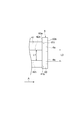
- FIG. 1 shows schematically the structure of the optical modulator which concerns on 1st Embodiment. It is a figure explaining arrangement
- FIG. 1 is a diagram schematically showing the configuration of an optical modulator that is a type of optical device according to the first embodiment of the present invention.
- the optical modulator 1 is a device that modulates input light introduced by the optical fiber F1 and outputs the modulated light to the optical fiber F2.
- the optical modulator 1 includes an optical input unit 2, a relay unit 3, an optical modulation element 4, a termination unit 5, a condensing member 6, a polarization beam combiner 7, an optical output unit 8, and a monitor unit 9. And the housing 10.
- the housing 10 is a box-shaped member extending in one direction (hereinafter referred to as “direction A”), and is made of, for example, stainless steel.
- the housing 10 has one end face 10a and the other end face 10b which are both end faces in the direction A.
- An opening for inserting the optical fiber F1 is provided in the one end face 10a.
- the housing 10 houses, for example, the light input unit 2, the relay unit 3, the light modulation element 4, the terminal unit 5, the light collecting member 6, the polarization beam combining unit 7, and the monitor unit 9.
- the light input unit 2 supplies input light introduced by the optical fiber F1 to the light modulation element 4.
- the light input unit 2 may include an auxiliary member for assisting the connection between the optical fiber F1 and the light modulation element 4.
- the relay unit 3 relays a modulation signal, which is an electric signal supplied from the outside, and outputs it to the light modulation element 4.
- the relay unit 3 inputs a modulation signal via a modulation signal input connector provided on the side surface 10 c of the housing 10, and outputs the modulation signal to the light modulation element 4.
- the light modulation element 4 is a device that converts input light supplied from the light input unit 2 into modulated light in accordance with a modulation signal output from the relay unit 3.
- the light modulation element 4 may include a substrate 41 (waveguide substrate), an optical waveguide 42, and a signal electrode 43.
- the substrate 41 is made of a dielectric material that exhibits an electro-optic effect, such as lithium niobate (LiNbO 3 , hereinafter referred to as “LN”).
- LNbO 3 lithium niobate
- a light modulation element using LN is called an LN light modulation element.
- the substrate 41 extends along the direction A and has one end 41a and the other end 41b that are both ends in the direction A.
- substrate a semiconductor or EO polymer etc. are mentioned besides a dielectric material.
- the optical waveguide 42 is provided on the substrate 41.
- the optical waveguide 42 is, for example, a Mach-Zehnder (MZ) type optical waveguide, and has a structure corresponding to the modulation method of the light modulation element 4.
- the modulation method of the light modulation element 4 is a DP-QPSK (Dual Polarization-Quadrature Phase Shift Keying) modulation method.
- the optical waveguide 42 includes an input waveguide 42a, a Mach-Zehnder portion 42d, a Mach-Zehnder portion 42e, an output waveguide 42b, and an output waveguide 42c.
- the input waveguide 42a extends from the one end portion 41a of the substrate 41 along the direction A, branches, and is connected to the input end of the Mach-Zehnder portion 42d and the input end of the Mach-Zehnder portion 42e, respectively.
- the output waveguide 42b extends along the direction A from the output end of the Mach-Zehnder portion 42d to the other end portion 41b.
- the output waveguide 42c extends in the direction A along a plane including the direction A (waveguide surface) from the output end of the Mach-Zehnder portion 42e to the other end 41b. That is, the direction A corresponds to the waveguide direction that is the extending direction of the waveguide.
- the signal electrode 43 is a member for applying an electric field according to the modulation signal to the optical waveguide 42, and is provided on the substrate 41.
- the arrangement and number of signal electrodes 43 are determined according to the orientation of the crystal axis of the substrate 41 and the modulation method of the light modulation element 4.
- a modulation signal output from the relay unit 3 is applied to each signal electrode 43.
- the input light input to the light modulation element 4 from the light input unit 2 is guided to the Mach-Zehnder unit 42d and the Mach-Zehnder unit 42e by the input waveguide 42a.
- the input light is modulated in the Mach-Zehnder part 42d and the Mach-Zehnder part 42e, respectively, and is output from the light modulation element 4 through the output waveguide 42b and the output waveguide 42c.
- the termination unit 5 is an electrical termination of the modulation signal.
- the termination unit 5 may include a resistor corresponding to each of the signal electrodes 43 of the light modulation element 4. One end of each resistor is electrically connected to the signal electrode 43 of the light modulation element 4, and the other end of each resistor is connected to the ground potential.
- the resistance value of each resistor is substantially equal to the characteristic impedance of the signal electrode 43, for example, about 50 ⁇ .
- the condensing member 6 condenses the modulated light output from the light modulation element 4.
- the condensing member 6 is provided on the other end 41 b (outgoing end surface) of the substrate 41.
- the condensing member 6 includes a base material 60 and, for example, condensing elements 6 a and 6 b on the other end surface 60 b facing the one end surface 60 a on the other end 41 b side of the substrate 41.
- the condensing elements 6a and 6b are, for example, condensing lenses.
- the base material 60 has a substantially rectangular parallelepiped shape, and has translucency similarly to the condensing elements 6a and 6b.
- the one end surface 60a and the other end surface 60b of the base member 60 are parallel to each other.
- the condensing element 6a is provided at the output end of the output waveguide 42b, receives light (first emitted light) emitted from the end on the other end 41b side of the output waveguide 42b, collimates and emits it. .
- the condensing element 6b is provided at the output end of the output waveguide 42c, and receives light (second emitted light) emitted from the end on the other end 41b side of the output waveguide 42c and collimates it.
- a diffractive lens such as a Fresnel lens or a holographic lens, a gradient index lens, or the like can be used.
- the condensing member 6 having the above-described configuration is the same as that of the base member 60 in a state where the condensing element 6a (first condensing element) and the condensing element 6b (second condensing element) are kept at a constant interval. It is preferable to realize as a lens array molded on the end surface 60b (element installation surface).
- the condensing member 6 can be manufactured by attaching the condensing elements 6a and 6b independently created on the surface of the base material 60, but the surface or the inside of the base material 60 can be manufactured by using a photo process or a molding technique. If it is formed as a lens array, the lens interval and performance are stable, which is more preferable.
- the condensing member 6 is a lens array in which the condensing element 6a and the condensing element 6b are attached to the substrate 60 will be described.
- the light condensed by the condensing member 6 is supplied to the polarization beam combiner 7.
- the polarization beam combiner 7 combines a plurality of modulated lights output from the light modulation element 4.
- the polarization beam combiner 7 can include a polarization rotation unit 71 and a polarization beam combiner 72.
- the polarization rotation unit 71 may include a polarization rotation element and a dummy element.
- the polarization rotation element is an element that rotates the polarization direction of incident light, and is, for example, a wave plate.
- the dummy element is an element that transmits the polarization direction of incident light without rotating.
- the polarization rotation unit 71 rotates, for example, 90 degrees in the polarization direction of either the modulated light output from the output waveguide 42b of the light modulation element 4 or the modulated light output from the output waveguide 42c, Do not rotate the polarization direction.
- one polarization direction may be rotated 45 degrees and the other may be rotated -45 degrees.
- the polarization beam combining element 72 is an element that changes the optical path according to the polarization direction of incident light, and is made of a birefringent crystal such as rutile or YVO 4 .
- the polarization beam combiner 72 combines the light whose polarization is rotated by the polarization rotation unit 71 and the light that is transmitted without being rotated by the polarization rotation unit 71.
- the polarization beam combining element 72 may be a polarization beam splitter (PBS). When a birefringent crystal is used, the two incident lights may be orthogonal to each other by rotating the polarization to ⁇ 45 ° and + 45 °.
- the light output unit 8 outputs the light combined by the polarization beam combiner 7 to the optical fiber F2.
- the light output unit 8 can include a window portion 81 and a condensing element 82.
- the window portion 81 is fitted into an opening provided on the other end surface 10 b of the housing 10.
- the window 81 is made of glass, for example, and transmits the light combined by the polarization beam combiner 7 to the outside of the housing 10.
- the condensing element 82 is provided outside the housing 10.
- the condensing element 82 is, for example, a condensing lens.
- the light transmitted through the window 81 is collected by the light collecting element 82 and output to the optical fiber F2.
- the monitor unit 9 monitors, for example, the complementary light intensity of the light outputs of the Mach-Zehnder units 42d and 42e.
- the monitor unit 9 can include a photoelectric conversion element.
- the photoelectric conversion element is an element for converting an optical signal into an electric signal, and is, for example, a photodiode.
- the photoelectric conversion element is placed on a waveguide branched from the output waveguide 42b of the Mach-Zehnder portion 42d on the substrate 41, receives an evanescent wave leaking from the waveguide, and outputs an electric signal corresponding to the light intensity. Output to a bias controller (not shown).
- the monitor unit 9 may monitor the light intensity of the radiated light output from the light modulation element 4.
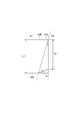
- FIG. 2 is a diagram for explaining the arrangement of the other end 41b of the substrate 41 and the light collecting member 6 in a general conventional modulator.
- the exit end face forming the other end portion 41b is provided such that the angle ⁇ 0 formed with the direction A is 90 °.
- light from the output waveguides 42b and 42c is emitted in the direction A from the other end 41b.
- the one end surface 60a of the base member 60 constituting the light collecting member 6 is attached so as to come into contact with the other end portion 41b, the light emitted from the output waveguides 42b and 42c is the base member 60 and the light collecting element, respectively.
- the light passes through 6a and 6b and is emitted from the light collecting elements 6a and 6b.
- the light emitted from 6a and 6b becomes parallel.
- L1 and L2 have a relationship of L1 ⁇ L2 or L1> L2
- at least one of the light emitted from the output waveguides 42b and 42c is different from the optical axis of the condensing elements 6a and 6b. It enters the condensing element at the position.
- the light emission direction is emitted in a direction different from the incident direction (direction A). For this reason, the optical paths of the two lights emitted from the condensing elements 6a and 6b are not parallel, and as a result, the light condensing efficiency in the light output unit 8 may be lowered.
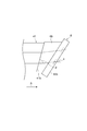
- the angle ⁇ formed by the other end portion 41 b (exit end face) of the substrate 41 and the direction A is 0 ° ⁇
- the other end surface 41b of the substrate 41 is arranged so that the other end surface 60b (element installation surface) where the condensing elements 6a and 6b of the condensing member 6 are provided and the other end portion 41b of the substrate 41 are parallel to each other.
- the condensing member 6 is attached.
- the refractive index of the light condensing element ⁇ the refractive index of the substrate
- the total reflection angle is excluded.
- ⁇ be an angle at which return light to the substrate can be cut sufficiently. For example, when LiNbO 3 is used for the substrate, the reflected return light can be sufficiently cut if it is 87 ° or less.
- the angle ⁇ parallel to the angle x is set based on the above relationship.
- the light converging elements 6a and 6b for the output waveguides 42b and 42c can be suitably arranged.
- the waveguide interval L1 is 499 ⁇ m due to manufacturing error or the like, and the interval L2 between the centers of the light collecting elements is 501 ⁇ m. there is a possibility.
- the difference between the light condensing element intervals L2 with respect to the optical waveguide interval L1 is made as small as possible, and the light is emitted from the condensing elements 6a and 6b due to the difference between L1 and L2.
- the optical paths of the two lights are not parallel to each other, and a reduction in light collection efficiency at the light output unit 8 can be suppressed.
- the angle ⁇ formed by the other end portion 41b (exit end face) of the waveguide substrate 41 and the direction A that is the traveling direction of the light emitted from the waveguide is 0.
- ⁇ 90 ° the positions of the emission ends of the two output waveguides 42b and 42c can be shifted from each other along the direction A.
- the condensing elements 6a and 6b adjust the mounting position of the condensing member 6 molded on the other end surface 60b, thereby the distance between the two output waveguides 42b and 42c, and the condensing member The distance between the six condensing elements 6a and 6b can be adjusted, and the amount of light output to the outside can be suitably maintained.
- the angle ⁇ formed by the other end 41b (exit end face) of the substrate 41 and the direction A is 0 ° ⁇
- FIG. 4 is an enlarged view of the other end portion 41b (exit end face) of the substrate 41 and the vicinity of the light collecting member 6 of the optical modulator 1A according to the second embodiment.
- the optical modulator 1A according to the present embodiment is different from the optical modulator according to the first embodiment in that the angle ⁇ formed between the other end portion 41b of the substrate 41 and the direction A, the one end surface 60a of the light collecting member 6, and the direction. The difference is that the angle x made with A is different.
- one end surface 60a of the light collecting member 6 is inclined with respect to the other end 41b of the substrate 41, and ⁇ ⁇ x.
- the medium inserted between the substrate 41 and the light collecting member 6 is not particularly limited as long as it is a medium that transmits light, such as air, an optical adhesive, and a glass wedge plate.
- the refractive index of the medium is preferably equal to that of the light collecting member.
- an antireflection film may be appropriately provided at the interface between the medium and the light collecting member.
- FIG. 1 A method of aligning the positions of the light converging elements 6a and 6b of the light condensing member 6 with respect to the two output waveguides 42b and 42c in a state where a medium is inserted between the substrate 41 and the light condensing member 6 is schematically shown in FIG. This will be described with reference to the drawings.
- the angle formed by the one end surface 60a of the member 6 is 90 ° ⁇ ( ⁇ / 2 ⁇ ).
- the distance between the two output waveguides 42b and 42c is L1
- the distance between the light converging elements 6a and 6b is L2
- the refractive index of the substrate 41 is n1
- the refractive index of the medium is n2.
- the angle ⁇ formed by the other end portion 41b (exit end face) of the substrate 41 and the direction A is 0 ° ⁇
- the distance L1 between the two output waveguides 42b and 42c is determined according to the refractive index of the medium.
- the distance L2 between the light condensing elements 6a and 6b can be changed, and the positions of the light converging elements 6a and 6b of the light condensing member 6 with respect to the two output waveguides 42b and 42c can be matched. Therefore, it is possible to more suitably maintain the amount of light output from the outside to the outside.
- FIGS. 3 and 4 A modification of the optical modulator 1A according to the second embodiment is shown in FIGS.
- the angle x formed by the main surface of the light collecting member 6 and the direction A may be 0 ° ⁇
- FIG. 6 schematically shows a case where the angle x formed between the main surface of the base material 60 and the direction A is larger than the angle ⁇ formed between the other end portion 41 b of the substrate 41 and the direction A ( ⁇ ⁇ x).
- FIG. 7 schematically shows the case where the angle x formed between the main surface of the substrate 60 and the direction A is smaller than the angle ⁇ formed between the other end portion 41b of the substrate 41 and the direction A ( ⁇ > x). ing.
- FIG.6 and FIG.7 the structure which inserted the glass wedge board 66 as a medium is shown.
- the glass wedge plate 66 is used as a medium between the substrate 41 and the light collecting member 6, it is easy to suitably fix the substrate 41 and the light collecting member 6 at a desired angle using a fixing jig or the like, for example.
- the angle x formed between the main surface of the base material 60 and the direction A can be made different from the angle ⁇ formed between the other end portion 41 b of the substrate 41 and the direction A, and , ⁇ and x can be changed as appropriate.
- the angles ⁇ and x are preferably determined based on the distance L1 between the two output waveguides 42b and 42c, the distance L2 between the light converging elements 6a and 6b, the difference between the refractive index of the substrate 41 and the refractive index of the medium, and the like. .
- FIG. 8 is an enlarged view of the other end portion 41b (exit end face) of the substrate 41 and the vicinity of the light collecting member 6 of the optical modulator 1B according to the third embodiment.
- an angle x0 formed by the one end surface 60a of the light collecting member 6 and the direction A and an angle x1 formed by the other end surface 60b provided with the light collecting elements 6a and 6b and the direction A are set.
- Different (x0 ⁇ x1) points That is, the base member 60 ′ of the light collecting member 6 is formed in a wedge shape, and the one end surface 60 a is connected to the substrate 41.
- condensing elements 6a and 6b are provided on the other end surface 60b.
- the function of the medium provided between the substrate 41 and the condensing member 6 is set to be similar to that of the optical modulator 1A of the second embodiment.
- the base material 60 is provided, and the positions of the condensing elements 6a and 6b of the condensing member 6 with respect to the two output waveguides 42b and 42c can be suitably set. Moreover, since it is not necessary to provide a medium between the board
- two output waveguides 42b are provided for an angle x0 formed by one end surface 60a of the light collecting member 6 and the direction A and an angle x1 formed by the other end surface 60b provided with the light collecting elements 6a and 6b and the direction A. , 42c, the distance L2 between the light condensing elements 6a and 6b, the difference between the refractive index of the substrate 41 and the refractive index of the base material 60 of the light condensing member 6, and the like.
- optical modulator according to the present embodiment has been described above, but the optical device according to the present invention is not limited to the above embodiment.
- the DP-QPSK modulation type optical modulator has been described in the above embodiment, two output waveguides are formed, and the first output light and the second output light that are parallel to each other are formed from these substrates. If it is an optical device provided with the board
- the concentrating elements 6 a and 6 b are installed on the surface of the base material 60, and the end surface 60 b is the element setting surface, but the positions of the condensing elements 6 a and 6 b are the surface of the base material 60. If they are not equidistant from each other, a plane that includes a straight line connecting the condensing elements 6a and 6b and that is perpendicular to the plane including the output waveguides 42b and 42c can be considered as the element installation surface.
- the straight line connecting the condensing elements 6a and 6b is, for example, the intersection of the main surface of the condensing element 6a and the principal ray of the first emitted light, the main surface of the condensing element 6b, and the second output. It is a straight line passing through the intersection with the chief ray of incident light. Therefore, the element installation surface is not limited to 60b described in the embodiment, but is a concept used in explaining the positional relationship (interval) between the two light collecting elements that are substantially fixed. If the collimating member 6 in which the positional relationship between the two condensing elements is fixed and the positional relationship (interval) between the first outgoing light and the second outgoing light can be efficiently collimated, the configuration of the present application can be achieved. It is included.
- the configuration of the optical modulator according to the first to third embodiments has been described above, the configurations described in the embodiments may be combined.
- a medium may be provided between the light collecting member 6 and the substrate 41.
- the waveguide interval and the lens interval of the lens array can be manufactured with almost no variation within the same lot.
Landscapes
- Physics & Mathematics (AREA)
- General Physics & Mathematics (AREA)
- Optics & Photonics (AREA)
- Optical Modulation, Optical Deflection, Nonlinear Optics, Optical Demodulation, Optical Logic Elements (AREA)
- Optical Couplings Of Light Guides (AREA)
- Optical Integrated Circuits (AREA)
- Engineering & Computer Science (AREA)
- Microelectronics & Electronic Packaging (AREA)
Abstract
導波路面に沿って2つの導波路42b、42cが形成され、出射端面41bにおいて該2つの導波路からそれぞれ第1、2の出射光が平行に出射される導波路基板41と、前記第1、2の出射光をそれぞれ入射してコリメートして出射する第1、2の集光素子が一定の間隔を保持した状態で素子設置面上に成型された集光部材6と、を有する光デバイスであって、導波路面内における前記出射端面と導波路方向Aとのなす角をθとしたときに、0°<|θ|<90°を満たす。前記θを適宜設定することにより、前記2つの導波路の間隔L1と前記第1、2の集光素子の間隔L2の製造誤差等に伴う、光路のズレが解消される。
Description
本発明は、光デバイスに関する。
100Gb/sの高速且つ大容量の光ファイバ通信を可能にする光デバイスとして、偏波直交4値位相変調器(DP-QPSK;Dual Polarization-Quadrature Phase Shift Keying)が知られている。例えば、特許文献1のDP-QPSKでは、LN基板上に2組のマッハツェンダ型の光導波路が設けられ、それぞれのマッハツェンダ型の光導波路から出射された光の一方または両方の偏波面を回転させ、これらの光の偏波面が互いに直交する関係で合波することにより偏波合成して出力している。偏波合成の光学系構成については、例えば特許文献2において、基板出射端面の近く配置されたレンズ(集光素子)でコリメート(集光)した後に1/2波長板で一方の偏波面を回転させ、ミラーと偏光ビームスプリッタ(PBS)によって合波して出射する構成が示されている。しかし、これらの構成では、一つ一つの光学系の取り付け、調整のためにスペースや工数を必要とするため、変調器のサイズや部材・組立コストの点で問題がある。この問題を解決するために、特許文献2の基板出射端の近くに取り付けられる集光素子として、例えば特許文献3に記載のように、2つの光路から出射された光がそれぞれ入射して平行に出射するレンズが配列形成されたレンズアレイ(集光部材)を用いることが考えられる。このようなレンズアレイや、ミラーやPBSが一体成型された偏波合成素子を用いることで、変調器のサイズ及び部材コストの低減や生産性の向上が期待される。
しかしながら、変調器に用いられる導波路の導波路間距離・レンズアレイのレンズ間距離には、それぞれ金型やフォトマスク等に由来する製造誤差が含まれる可能性がある。具体的には、製造誤差として1μm程度の誤差が各部材に発生すると考えると、両者の製造誤差を加味すると最大2μm程度のずれが生じる可能性がある。この場合、2つの導波路から出射された光が互いに平行とならないなど設計上の光路とずれる等の理由によって、変調器から外部へ出力するための光出力部との結合効率が低くなり、変調器から出射される光の光量が減少することが考えられる。
本発明は、上記を鑑みてなされたものであり、外部へ出力する光の光量を好適に維持することが可能な光デバイスを提供することを目的とする。
本発明の一側面に係る光デバイスは、導波路面に沿って2つの導波路が形成され、該導波路面とは異なる出射端面において該2つの導波路からそれぞれ出射される第1の出射光及び第2の出射光が平行に出射される導波路基板と、前記第1の出射光を入射してコリメートして出射する第1の集光素子と、前記第2の出射光を入射してコリメートして出射する第2の集光素子と、が一定の間隔を保持した状態で素子設置面上に成型された集光部材と、を有する光デバイスであって、前記導波路面内における前記導波路基板の出射端面と前記導波路の延在方向である導波路方向とのなす角をθとしたときに、0°<|θ|<90°を満たすことを特徴とする。
上記の光デバイスによれば、光導波路基板の出射端面と導波路方向とのなす角θを0°<|θ|<90°とすることにより、2つの導波路の導波路基板からの出射端の位置を導波路方向に沿って互いにずらすことができる。これに対して、第1の集光素子と第2の集光素子とが素子設置面上に成型された集光部材の取り付け位置を調整することで、2つの導波路間の距離と、集光部材の2つのレンズ間の距離と、の調整が可能となり、外部へ出力する光の光量を好適に維持することが可能となる。
ここで、上記作用を効果的に奏する構成として、具体的には、導波路基板の出射端面と導波路方向とのなす角θは、第1の出射光と第2の出射光との間の距離と、第1の集光素子と第2の集光素子との間の距離と、に基づいて決定される態様が挙げられる。
また、素子設置面と導波路方向とのなす角をxとしたときに、θ=xである態様とすることができる。
また、素子設置面と導波路方向とのなす角をxとしたときに、θ≠xである態様としてもよい。
ここで、集光部材と導波路基板の出射端面との間の第1の集光素子から出射される光の光路上及び第2の集光素子から出射される光の光路上に、導波路とは屈折率が異なる媒質をさらに備える態様とすることもできる。
集光部材の素子設置面は、第1の出射光及び第2の出射光が入射する端面とは逆側に設けられ、第1の出射光及び第2の出射光が入射する端面と導波路方向とのなす角はxとは異なる態様とすることができる。
このように、集光部材の素子設置面と入射側の端面とを互いに平行とはせず、異なる角度としてもよい。導波路の間隔又はレンズの間隔に応じて、集光部材の形状を適宜変更することで、外部へ出力する光の光量を好適に維持する環境をより好適に実現することができる。
本発明の一側面によれば、外部へ出力する光の光量を好適に維持することが可能な光デバイスが提供される。
以下、添付図面を参照して本発明の実施形態を詳細に説明する。
(第1実施形態)
図1は、本発明の第1実施形態に係る光デバイスの一種である光変調器の構成を概略的に示す図である。図1に示されるように、光変調器1は、光ファイバF1によって導入された入力光を変調して、光ファイバF2に変調光を出力する装置である。光変調器1は、光入力部2と、中継部3と、光変調素子4と、終端部5と、集光部材6と、偏波合成部7と、光出力部8と、モニタ部9と、筐体10と、を備え得る。
図1は、本発明の第1実施形態に係る光デバイスの一種である光変調器の構成を概略的に示す図である。図1に示されるように、光変調器1は、光ファイバF1によって導入された入力光を変調して、光ファイバF2に変調光を出力する装置である。光変調器1は、光入力部2と、中継部3と、光変調素子4と、終端部5と、集光部材6と、偏波合成部7と、光出力部8と、モニタ部9と、筐体10と、を備え得る。
筐体10は、一方向(以下、「方向A」という。)に延びる箱型の部材であって、例えばステンレス鋼から構成されている。筐体10は、方向Aにおける両端面である一端面10a及び他端面10bを有する。一端面10aには光ファイバF1を挿入するための開口が設けられている。筐体10は、例えば、光入力部2、中継部3、光変調素子4、終端部5、集光部材6、偏波合成部7及びモニタ部9を収容する。
光入力部2は、光ファイバF1によって導入される入力光を光変調素子4に供給する。光入力部2は、光ファイバF1と光変調素子4との接続を補助するための補助部材を備えてもよい。
中継部3は、外部から供給される電気信号である変調信号を中継して光変調素子4に出力する。中継部3は、例えば筐体10の側面10cに設けられた変調信号入力用のコネクタを介して変調信号を入力し、光変調素子4に変調信号を出力する。
光変調素子4は、中継部3から出力される変調信号に応じて、光入力部2から供給される入力光を変調光に変換する装置である。光変調素子4は、基板41(導波路基板)と、光導波路42と、信号電極43と、を備え得る。基板41は、例えばニオブ酸リチウム(LiNbO3、以下「LN」という。)などの電気光学効果を奏する誘電体材料から構成されている。LNを用いた光変調素子をLN光変調素子と呼ぶ。基板41は方向Aに沿って延びており、方向Aにおける両端部である一端部41a及び他端部41bを有する。また、基板を構成する材料としては、誘電体材料の他に、半導体又はEOポリマー等が挙げられる。
光導波路42は、基板41上に設けられている。光導波路42は、例えばマッハツェンダ(Mach-Zehnder:MZ)型の光導波路であって、光変調素子4の変調方式に応じた構造を有する。この例では、光変調素子4の変調方式は、DP-QPSK(Dual Polarization-Quadrature Phase Shift Keying:偏波直交4値位相変調)変調方式である。この場合、光導波路42は、入力導波路42aと、マッハツェンダ部42dと、マッハツェンダ部42eと、出力導波路42bと、出力導波路42cと、を備える。入力導波路42aは基板41の一端部41aから方向Aに沿って延び、分岐されてマッハツェンダ部42dの入力端及びマッハツェンダ部42eの入力端にそれぞれ接続されている。出力導波路42bは、マッハツェンダ部42dの出力端から他端部41bまで方向Aに沿って延びている。出力導波路42cは、マッハツェンダ部42eの出力端から他端部41bまで方向Aを含む面(導波路面)に沿って方向Aへ向かって延びている。すなわち、方向Aは、導波路の延在方向である導波路方向に相当する。
信号電極43は、変調信号に応じた電界を光導波路42に印加するための部材であって、基板41上に設けられている。信号電極43の配置及び数は、基板41の結晶軸の向き及び光変調素子4の変調方式に応じて決定される。各信号電極43には、中継部3から出力される変調信号がそれぞれ印加される。
光変調素子4では、光入力部2から光変調素子4に入力される入力光は、入力導波路42aによってマッハツェンダ部42d及びマッハツェンダ部42eに導かれる。入力光は、マッハツェンダ部42d及びマッハツェンダ部42eにおいてそれぞれ変調され、出力導波路42b及び出力導波路42cを通って光変調素子4から出力される。
終端部5は、変調信号の電気的終端である。終端部5は、光変調素子4の信号電極43の各々に対応した抵抗器を備え得る。各抵抗器の一端は光変調素子4の信号電極43に電気的に接続され、各抵抗器の他端は接地電位に接続されている。各抵抗器の抵抗値は、信号電極43の特性インピーダンスと略等しく、例えば50Ω程度である。
集光部材6は、光変調素子4から出力される変調光を集光する。集光部材6は、基板41の他端部41b(出射端面)に設けられている。集光部材6は、基材60と、基板41の他端部41b側の一端面60aと対向する他端面60b上に例えば集光素子6a,6bと、を含んで構成される。集光素子6a,6bは、例えば集光レンズである。基材60は、略直方体形状を有し、集光素子6a,6bと同様に透光性を有する。基材60の一端面60aと他端面60bとは互いに平行である。集光素子6aは出力導波路42bの出力端に設けられ、出力導波路42bの他端部41b側の端部から出射される光(第1の出射光)を入力し、コリメートして出射する。また、集光素子6bは出力導波路42cの出力端に設けられ、出力導波路42cの他端部41b側の端部から出射される光(第2の出射光)を入力し、コリメートして出射する。集光レンズとしては、一般的な球面レンズの他に、フレネルレンズ、ホログラフィックレンズなどの回折型レンズ、屈折率分布型レンズ、などを用いることが可能である。
上記の構成を有する集光部材6は、集光素子6a(第1の集光素子)及び集光素子6b(第2の集光素子)が一定の間隔を保持した状態で基材60の他端面60b(素子設置面)上に成型されたレンズアレイとして実現するのが好適である。集光部材6は、基材60の表面にそれぞれ独立に作成した集光素子6a、6bを貼り付けることでも製造可能だが、フォトプロセス又はモールド成型技術等を用いて、基材60の表面又は内部にレンズアレイとして成形すると、レンズ間隔及び性能が安定して、より好適である。以下の実施形態では、集光部材6が、集光素子6a及び集光素子6bが基材60に対して取り付けられたレンズアレイである場合について説明する。集光部材6によって集光された光は、偏波合成部7に供給される。
偏波合成部7は、光変調素子4から出力される複数の変調光を合成する。偏波合成部7は、偏波回転部71と、偏波合成素子72と、を備え得る。偏波回転部71は、偏波回転素子と、ダミー素子と、を有してもよい。偏波回転素子は、入射光の偏波方向を回転する素子であって、例えば波長板である。ダミー素子は、入射光の偏波方向を回転することなく透過する素子である。偏波回転部71は、光変調素子4の出力導波路42bから出力される変調光と出力導波路42cから出力される変調光とのいずれか一方の偏波方向を例えば90度回転し、他方の偏波方向を回転しない。なお、別の例として一方の偏波方向を45度回転し、他方を-45度回転しても良い。
偏波合成素子72は、入射光の偏波方向に応じて光路を変える素子であって、例えばルチル、YVO4などの複屈折結晶から構成されている。偏波合成素子72は、偏波回転部71によって偏波回転される光と、偏波回転部71によって偏波回転されずに透過する光と、を合成する。また、偏波合成素子72は、偏光ビームスプリッタ(Polarization Beam Splitter:PBS)であってもよい。なお、複屈折結晶を用いる場合は、偏波を-45°と+45°に回転することで2つの入射光を互いに直交させる構成としてもよい。
光出力部8は、偏波合成部7によって合成された光を光ファイバF2に出力する。光出力部8は、窓部81と、集光素子82と、を備え得る。窓部81は、筐体10の他端面10bに設けられた開口に嵌め込まれている。窓部81は、例えばガラスから構成されており、偏波合成部7によって合成された光を筐体10の外部に透過する。集光素子82は、筐体10の外部に設けられている。集光素子82は例えば集光レンズである。窓部81を透過した光は、集光素子82によって集光され、光ファイバF2に出力される。
モニタ部9は、例えば、各マッハツェンダ部42d,42eの光出力の相補的な光強度をモニタする。モニタ部9は光電変換素子を備え得る。光電変換素子は、光信号を電気信号に変換するための素子であって、例えばフォトダイオードである。光電変換素子は、例えば基板41上で、マッハツェンダ部42dの出力導波路42bと分岐した導波路上に置かれ、導波路から漏れだしたエバネッセント波を受光し、その光強度に応じた電気信号をバイアス制御部(不図示)に出力する。なお、モニタ部9は、光変調素子4から出力される放射光の光強度をモニタしてもよい。
ここで、本発明の特徴をなす部分である基板41の他端部41b(出射端面)及び集光部材6の形状について、図2及び図3を用いて説明する。図2は、一般的な従来の変調器における基板41の他端部41bと集光部材6との配置について説明する図である。
図2に示すように、従来の光変調器1’における基板41の他端部41bでは、他端部41bを形成する出射端面は方向Aとのなす角θ0が90°となるように設けられることで、出力導波路42b,42cからの光は他端部41bから方向Aに向けて出射される。集光部材6を構成する基材60の一端面60aは、他端部41bと当接するように取り付けられる場合、出力導波路42b,42cから出射された光は、それぞれ基材60及び集光素子6a,6bを通過して、集光素子6a,6bから出射される。ここで、2つの出力導波路42b,42c間の距離をL1とし、2つの集光素子6a,6b間の距離をL2としたときに、L1=L2の関係である場合には、集光素子6a,6bから出射される光は平行となる。しかしながら、L1とL2とがL1<L2又はL1>L2の関係となる場合には、出力導波路42b,42cから出射された光の少なくとも一方は、集光素子6a,6bの光軸とは異なる位置で集光素子に入射する。集光素子の光軸とは異なる位置で集光素子に入射した光が集光素子から出射されるとき、光の出射方向は入射方向(方向A)とは異なる方向に出射される。このため、集光素子6a,6bから出射される2つの光の光路は平行とはならず、その結果、光出力部8における光の集光効率が低下する可能性がある。
これに対して、図3に示すように、本実施形態に係る光変調器1では、基板41の他端部41b(出射端面)と方向Aとのなす角θが0°<|θ|<90°となるように方向Aに対して傾けられる。そして、集光部材6の集光素子6a,6bが設けられる他端面60b(素子設置面)と、基板41の他端部41bとが互いに平行となるように、基板41の他端部41bに対して集光部材6が取り付けられる。これにより集光素子6a,6bが設けられる他端面60bと方向Aとのなす角xは、θ=xを満たすと共に0°<|x|<90°とされる。ただし、集光素子の屈折率<基板の屈折率の場合、全反射角を除外する。例えば屈折率を1.5の集光素子と、屈折率2.2のLiNbO3基板を用いる場合、全反射角はθ=47°となるため、θは47°以上であることが好ましい。さらに、θは基板への戻り光が十分にカットできる角度であることが望ましい。例えば基板にLiNbO3を用いる場合は87°以下であれば反射戻り光を十分にカットできる。
このとき、基板41の出射端面と方向Aとのなす角θ(及び集光部材6の他端面60bと方向Aとのなす角x)は、L1<L2において、L2sinθ=L1(L2sinx=L1)の関係を満たすように設定する。
これにより、2つの出力導波路42b,42cの間隔L1と、集光素子6a,6bの間隔L2とが互いに異なる場合に、角xと平行な角θを上記の関係に基づいて設定することで、出力導波路42b,42cに対する集光素子6a,6bを好適に配置することが可能となる。具体的には、例えば、光変調器1における設計値をL1=L2=500μmとした場合に、製造誤差等により導波路間隔L1が499μmとなり、集光素子の中心間の間隔L2が501μmとなる可能性がある。この場合には、L2sinθ=L1となるように、θ=x=84.9°となるように他端部41b(出射端面)を傾けた状態で、集光部材6を基板41に対して固定して光変調器1を作成することにより、光導波路間隔L1に対する集光素子間隔L2の差分をできるだけ小さくし、L1とL2との差が原因となって集光素子6a,6bから出射される2つの光の光路が互いに平行とならず、光出力部8における光の集光効率の低下を抑制することができる。
このように、本実施形態に係る光変調器1では、導波路基板41の他端部41b(出射端面)と導波路から出射される光の進行方向である方向Aとのなす角θを0°<|θ|<90°とすることにより、2つの出力導波路42b,42cの出射端の位置を方向Aに沿って互いにずらすことができる。これに対して、集光素子6a,6bとが他端面60b上に成型された集光部材6の取り付け位置を調整することで、2つの出力導波路42b,42c間の距離と、集光部材6の集光素子6a,6b間の距離と、の調整が可能となり、外部へ出力する光の光量を好適に維持することが可能となる。
また、上記実施形態の光変調器1では、基板41の他端部41b(出射端面)と方向Aとのなす角θが0°<|θ|<90°となるように方向Aに対して傾けられると共に、集光部材6の集光素子6a,6bが設けられる他端面60bと方向Aとのなす角xはθ=xを満たす。これにより、2つの出力導波路42b,42c間の距離と、集光部材6の集光素子6a,6b間の距離との差異に基づいた角xの決定が容易になり、光変調器1の各部材についての簡単な調整で外部へ出力する光の光量を好適に維持することが可能となる。
(第2実施形態)
次に、第2実施形態に係る光変調器について説明する。第2実施形態以降の光変調器においては、基板41の他端部41b(出射端面)と方向Aとのなす角θと、集光部材6の集光素子6a,6bが設けられる他端面60bと方向Aとのなす角xとが互いに異なる場合について説明する。
次に、第2実施形態に係る光変調器について説明する。第2実施形態以降の光変調器においては、基板41の他端部41b(出射端面)と方向Aとのなす角θと、集光部材6の集光素子6a,6bが設けられる他端面60bと方向Aとのなす角xとが互いに異なる場合について説明する。
図4は、第2実施形態に係る光変調器1Aの基板41の他端部41b(出射端面)及び集光部材6近傍を拡大した図である。本実施形態に係る光変調器1Aが第1実施形態の光変調器と異なる点は、基板41の他端部41bと方向Aとのなす角θと、集光部材6の一端面60aと方向Aとのなす角xとが異なる点である。図4の光変調器1Aでは、基板41の他端部41bに対して集光部材6の一端面60aが傾いた状態であり、θ≠xとなっている。そして、基板41の他端部41bと集光部材6の一端面60aとの間の空隙には、基板41と異なる屈折率を有する媒質として、基板41と集光部材6とを固定する接着剤65が充填されている場合について説明する。なお、基板41と集光部材6との間に挿入される媒質としては、空気、光学接着剤、ガラスウェッジ板等、光を透過する媒質であれば特に制限されない。なお、媒質と集光部材との界面における光の反射を防ぐ目的から、媒質の屈折率は集光部材と同等であることが好ましい。あるいは、媒質と集光部材との界面に適宜反射防止膜を施してもよい。
基板41と集光部材6との間に媒質が挿入された状態で、2つの出力導波路42b,42cに対する集光部材6の集光素子6a,6bの位置を合わせる方法について、図5の模式図を用いて説明する。ここでは、簡単のために集光部材6の一端面60a(及び他端面60b)は方向Aに対して垂直であると仮定し(x=90°)、基板41の他端部41bと集光部材6の一端面60aのなす角を90°-θ(π/2-θ)とする。この条件で、2つの出力導波路42b,42cの間隔をL1とし、集光素子6a,6bの間隔をL2とし、基板41の屈折率をn1とし、媒質(接着剤65)の屈折率をn2としたとき、
L2=L1(1-1/tanθ・[tan{θ-cos-1(n1/n2×cosθ)}])
という関係が成り立つ。したがって、例えば、L1=500μm、n1=2.2、n2=1.5、θ=85°だとすると、L2=498μmとなる。また、媒質の屈折率n2を変えると、これに応じて、L2は変動する。したがって、屈折率の異なる媒質を選択することにより、基板41の他端部41bと集光部材6の一端面60aのなす角(90°-θ)を変更することなく、L1とL2との関係を変更して、2つの出力導波路42b,42cに対する集光部材6の集光素子6a,6bの位置を合わせることが可能となる。なお、第1実施形態は、L1<L2のケースに対応したが、本実施形態では、前述のようにL1>L2のケースにも対応が可能である。
L2=L1(1-1/tanθ・[tan{θ-cos-1(n1/n2×cosθ)}])
という関係が成り立つ。したがって、例えば、L1=500μm、n1=2.2、n2=1.5、θ=85°だとすると、L2=498μmとなる。また、媒質の屈折率n2を変えると、これに応じて、L2は変動する。したがって、屈折率の異なる媒質を選択することにより、基板41の他端部41bと集光部材6の一端面60aのなす角(90°-θ)を変更することなく、L1とL2との関係を変更して、2つの出力導波路42b,42cに対する集光部材6の集光素子6a,6bの位置を合わせることが可能となる。なお、第1実施形態は、L1<L2のケースに対応したが、本実施形態では、前述のようにL1>L2のケースにも対応が可能である。
第2実施形態に示す光変調器1Aのように、基板41の他端部41b(出射端面)と方向Aとのなす角θが0°<|θ|<90°となるように方向Aに対して傾けられると共に、集光部材6の集光素子6a,6bが設けられる他端面60bと方向Aとのなす角xはθ≠xを満たす関係である場合でも、光変調器1Aから外部へ出力する光の光量を好適に維持することが可能となる。
さらに、基板41と集光部材6との間に屈折率が基板41と異なる媒質を挿入する構成とした場合には、媒質の屈折率に応じて、2つの出力導波路42b,42cの間隔L1と集光素子6a,6bの間隔L2との関係を変更して、2つの出力導波路42b,42cに対する集光部材6の集光素子6a,6bの位置を合わせることができ、光変調器1Aから外部へ出力する光の光量の維持をより好適に行うことができる。
なお、第2実施形態に係る光変調器1Aの変形例を図6及び図7に示す。図3及び図4に示す光変調器1Aでは、集光部材6の一端面60a及び他端面60bが方向Aに対して垂直である場合について説明したが、基材60の一端面60a及び他端面60bが互いに平行であるとすると、集光部材6の主面と方向Aとのなす角xが0°<|x|<90°となる構成としてもよい。
図6は、基板41の他端部41bと方向Aとのなす角θよりも基材60の主面と方向Aとのなす角xが大きい場合(θ<x)について模式的に示している。また、図7では、基板41の他端部41bと方向Aとのなす角θよりも基材60の主面と方向Aとのなす角xが小さい場合(θ>x)について模式的に示している。また、図6及び図7では、媒質として、ガラスウェッジ板66を挿入した構成を示している。ガラスウェッジ板66を基板41と集光部材6との間の媒質として用いる場合、例えば固定治具等を用いて基板41及び集光部材6を所望の角度に好適に固定しやすくなる。
図5~図7に示すように、基板41の他端部41bと方向Aとのなす角θよりも基材60の主面と方向Aとのなす角xとは異ならせることができ、さらに、θとxとの角度は適宜変更することができる。θ及びxの角度は、2つの出力導波路42b,42cの間隔L1、集光素子6a,6bの間隔L2、基板41の屈折率と媒質の屈折率との差等に基づいて決めることが好ましい。
(第3実施形態)
次に、第3実施形態に係る光変調器について説明する。第3実施形態以降の光変調器においては、集光素子6a,6bの形状が第1実施形態及び第2実施形態と相違する。
次に、第3実施形態に係る光変調器について説明する。第3実施形態以降の光変調器においては、集光素子6a,6bの形状が第1実施形態及び第2実施形態と相違する。
図8は、第3実施形態に係る光変調器1Bの基板41の他端部41b(出射端面)及び集光部材6近傍を拡大した図である。本実施形態に係る光変調器1Bでは、集光部材6の一端面60aと方向Aとのなす角x0と、集光素子6a,6bが設けられる他端面60bと方向Aとのなす角x1が異なる(x0≠x1)点である。すなわち、集光部材6の基材60’がウェッジ状に成型されていて、一端面60aは基板41と接続する。一方で、他端面60bに集光素子6a,6bが設けられている。
このような構成を有する集光部材6を用いる場合には、第2実施形態の光変調器1Aのように、基板41と集光部材6との間に設けられる媒質の機能を集光部材6の基材60が備え、2つの出力導波路42b,42cに対する集光部材6の集光素子6a,6bの位置を好適に設定することができる。また、基板41と集光部材6との間に媒質を設けなくてもよいので、部品点数を減らすこともできる。
なお、集光部材6の一端面60aと方向Aとのなす角x0、及び、集光素子6a,6bが設けられる他端面60bと方向Aとのなす角x1については、2つの出力導波路42b,42cの間隔L1、集光素子6a,6bの間隔L2、基板41の屈折率と集光部材6の基材60の屈折率との差等に基づいて決めることが好ましい。
以上、本実施形態に係る光変調器について説明したが、本発明に係る光デバイスは上記実施形態に限定されない。例えば、上記実施形態ではDP-QPSK変調方式の光変調器について説明をしたが、2つの出力導波路が形成されて、これらの基板から互いに平行な第1の出射光及び第2の出射光を出射する基板と、第1の出射光及び第2の出射光のそれぞれを個別にコリメートして出射する2つの集光素子を備える集光部と、を備える光デバイスであれば、本発明の構成を適用することができる。なお、以上の説明では、基材60の表面に集光素子6a、6bを設置するものとして、端面60bを素子設置面としたが、集光素子6a、6bの位置が、基材60の表面から等距離にない場合は、集光素子6a、6bを結ぶ直線を含み、出力導波路42b、42cを含む面に垂直な面を素子設置面と考えることができる。ここで、集光素子6a、6bを結ぶ直線とは、例えば、集光素子6aの主面と第1の出射光の主光線との交点と、集光素子6bの主面と第2の出射光の主光線との交点とを通る直線である。したがって、素子設置面とは実施例で記載の60bに限定されるものではなく、実質的には固定された2つの集光素子の位置関係(間隔)を説明する上で使用した概念であり、当該2つの集光素子の位置関係が固定された集光部材6と、第1の出射光及び第2の出射光との位置関係(間隔)を調整することで効率よくコリメートできれば本願の構成に含まれるものである。
また、上記では第1~第3実施形態に係る光変調器の構成について説明をしているが、各実施形態に記載の構成を組み合わせてもよい。例えば、集光部材6の基材61の形状をウェッジ状としたうえで、集光部材6と基板41との間に媒質を設ける構成とすることもできる。
また、本発明に係る光デバイスを量産する場合には、導波路間隔及びレンズアレイのレンズ間隔は、同じロット内ではほぼばらつきなく製造することができるので、製造された部材における導波路間隔及びレンズ間隔を実測し、その結果に基づいて、基板41の他端部41bの角度θ、集光部材6の端面60bの角度x、その他集光部材6の形状等を一度決定すれば、そのロット内では同じ設定で製造することも可能であり、高精度で安定した製品を効率よく製造することが可能である。
1,1A,1B…光変調器、2…光入力部、3…中継部、4…光変調素子、5…終端部、6…集光部材、6a,6b…集光素子、7…偏波合成部、8…光出力部、9…モニタ部、10…筐体、41…基板、42b,42c…出力導波路、60…基材。
Claims (6)
- 導波路面に沿って2つの導波路が形成され、該導波路面とは異なる出射端面において該2つの導波路からそれぞれ出射される第1の出射光及び第2の出射光が平行に出射される導波路基板と、
前記第1の出射光を入射してコリメートして出射する第1の集光素子と、前記第2の出射光を入射してコリメートして出射する第2の集光素子と、が一定の間隔を保持した状態で素子設置面上に成型された集光部材と、
を有する光デバイスであって、
前記導波路面内における前記導波路基板の出射端面と前記導波路の延在方向である導波路方向とのなす角をθとしたときに、0°<|θ|<90°を満たすことを特徴とする光デバイス。 - 前記導波路基板の出射端面と前記導波路方向とのなす角θは、
前記第1の出射光と前記第2の出射光との間の距離と、前記第1の集光素子と前記第2の集光素子との間の距離と、に基づいて決定されることを特徴とする請求項1記載の光デバイス。 - 前記素子設置面と前記導波路方向とのなす角をxとしたときに、
θ=xであることを特徴とする請求項1又は2記載の光デバイス。 - 前記素子設置面と前記導波路方向とのなす角をxとしたときに、
θ≠xであることを特徴とする請求項1又は2記載の光デバイス。 - 前記集光部材と前記導波路基板の出射端面との間の前記第1の集光素子から出射される光の光路上及び第2の集光素子から出射される光の光路上に、前記導波路とは屈折率が異なる媒質をさらに備えることを特徴とする請求項4記載の光デバイス。
- 前記集光部材の素子設置面は、前記第1の出射光及び前記第2の出射光が入射する端面とは逆側に設けられ、
前記第1の出射光及び前記第2の出射光が入射する端面と前記導波路方向とのなす角は前記xとは異なることを特徴とする請求項4記載の光デバイス。
Priority Applications (2)
| Application Number | Priority Date | Filing Date | Title |
|---|---|---|---|
| CN201480009914.2A CN105008973A (zh) | 2013-02-21 | 2014-02-19 | 光设备 |
| US14/768,888 US20160011377A1 (en) | 2013-02-21 | 2014-02-19 | Optical device |
Applications Claiming Priority (2)
| Application Number | Priority Date | Filing Date | Title |
|---|---|---|---|
| JP2013-032404 | 2013-02-21 | ||
| JP2013032404A JP5621861B2 (ja) | 2013-02-21 | 2013-02-21 | 光デバイス |
Publications (1)
| Publication Number | Publication Date |
|---|---|
| WO2014129506A1 true WO2014129506A1 (ja) | 2014-08-28 |
Family
ID=51391292
Family Applications (1)
| Application Number | Title | Priority Date | Filing Date |
|---|---|---|---|
| PCT/JP2014/053940 Ceased WO2014129506A1 (ja) | 2013-02-21 | 2014-02-19 | 光デバイス |
Country Status (4)
| Country | Link |
|---|---|
| US (1) | US20160011377A1 (ja) |
| JP (1) | JP5621861B2 (ja) |
| CN (1) | CN105008973A (ja) |
| WO (1) | WO2014129506A1 (ja) |
Cited By (1)
| Publication number | Priority date | Publication date | Assignee | Title |
|---|---|---|---|---|
| CN111886536A (zh) * | 2018-03-27 | 2020-11-03 | 住友大阪水泥股份有限公司 | 光调制装置 |
Families Citing this family (9)
| Publication number | Priority date | Publication date | Assignee | Title |
|---|---|---|---|---|
| JP6540576B2 (ja) | 2016-03-31 | 2019-07-10 | 住友大阪セメント株式会社 | 光変調デバイス |
| JP6269710B2 (ja) * | 2016-03-31 | 2018-01-31 | 住友大阪セメント株式会社 | 光変調デバイス |
| WO2017170194A1 (ja) * | 2016-03-31 | 2017-10-05 | 住友大阪セメント株式会社 | 光変調デバイス |
| JP6769378B2 (ja) * | 2017-03-31 | 2020-10-14 | 住友大阪セメント株式会社 | 光変調器 |
| CN113631985A (zh) * | 2020-02-20 | 2021-11-09 | 国立大学法人福井大学 | 光扫描型影像投影装置 |
| JP7452190B2 (ja) | 2020-03-31 | 2024-03-19 | 住友大阪セメント株式会社 | 光導波路素子及びそれを用いた光変調デバイス並びに光送信装置 |
| JP7380389B2 (ja) | 2020-03-31 | 2023-11-15 | 住友大阪セメント株式会社 | 光導波路素子及びそれを用いた光変調デバイス並びに光送信装置 |
| US11112574B1 (en) * | 2020-04-30 | 2021-09-07 | Hewlett Packard Enterprise Development Lp | Optoelectronic system with a wedge-shaped adapter |
| JP7533856B2 (ja) * | 2020-05-26 | 2024-08-14 | 富士通オプティカルコンポーネンツ株式会社 | 光変調器 |
Citations (4)
| Publication number | Priority date | Publication date | Assignee | Title |
|---|---|---|---|---|
| WO2008099950A1 (ja) * | 2007-02-14 | 2008-08-21 | Ngk Insulators, Ltd. | 光変調器用部品および光変調器 |
| JP2010286770A (ja) * | 2009-06-15 | 2010-12-24 | Fujitsu Optical Components Ltd | 光デバイス |
| JP2011203377A (ja) * | 2010-03-24 | 2011-10-13 | Nippon Telegr & Teleph Corp <Ntt> | 光モジュール |
| JP2012047953A (ja) * | 2010-08-26 | 2012-03-08 | Sumitomo Osaka Cement Co Ltd | 偏波制御装置 |
Family Cites Families (4)
| Publication number | Priority date | Publication date | Assignee | Title |
|---|---|---|---|---|
| US4623225A (en) * | 1984-06-29 | 1986-11-18 | Melles Griot, Irvine Company | Anamorphic prism for beam shaping |
| US4759616A (en) * | 1985-08-26 | 1988-07-26 | Eastman Kodak Company | Method and apparatus for anamorphically shaping and deflecting electromagnetic beams |
| US20110268387A1 (en) * | 2010-04-28 | 2011-11-03 | Gregor Popp | Two Dimensional Fiber Collimator Array With High Return Loss |
| JP5180341B2 (ja) * | 2011-04-19 | 2013-04-10 | 日本電信電話株式会社 | 光部品 |
-
2013
- 2013-02-21 JP JP2013032404A patent/JP5621861B2/ja active Active
-
2014
- 2014-02-19 CN CN201480009914.2A patent/CN105008973A/zh active Pending
- 2014-02-19 WO PCT/JP2014/053940 patent/WO2014129506A1/ja not_active Ceased
- 2014-02-19 US US14/768,888 patent/US20160011377A1/en not_active Abandoned
Patent Citations (4)
| Publication number | Priority date | Publication date | Assignee | Title |
|---|---|---|---|---|
| WO2008099950A1 (ja) * | 2007-02-14 | 2008-08-21 | Ngk Insulators, Ltd. | 光変調器用部品および光変調器 |
| JP2010286770A (ja) * | 2009-06-15 | 2010-12-24 | Fujitsu Optical Components Ltd | 光デバイス |
| JP2011203377A (ja) * | 2010-03-24 | 2011-10-13 | Nippon Telegr & Teleph Corp <Ntt> | 光モジュール |
| JP2012047953A (ja) * | 2010-08-26 | 2012-03-08 | Sumitomo Osaka Cement Co Ltd | 偏波制御装置 |
Cited By (2)
| Publication number | Priority date | Publication date | Assignee | Title |
|---|---|---|---|---|
| CN111886536A (zh) * | 2018-03-27 | 2020-11-03 | 住友大阪水泥股份有限公司 | 光调制装置 |
| CN111886536B (zh) * | 2018-03-27 | 2024-01-16 | 住友大阪水泥股份有限公司 | 光调制装置 |
Also Published As
| Publication number | Publication date |
|---|---|
| JP5621861B2 (ja) | 2014-11-12 |
| US20160011377A1 (en) | 2016-01-14 |
| CN105008973A (zh) | 2015-10-28 |
| JP2014163993A (ja) | 2014-09-08 |
Similar Documents
| Publication | Publication Date | Title |
|---|---|---|
| JP5621861B2 (ja) | 光デバイス | |
| JP4740994B2 (ja) | 光変調器 | |
| US11075500B2 (en) | Optical device having a substrate and a laser unit that emits light into the substrate | |
| JP4937325B2 (ja) | 光導波路デバイス | |
| JP5573985B1 (ja) | 光変調器 | |
| JP6769378B2 (ja) | 光変調器 | |
| CN104321690A (zh) | 光调制器 | |
| CN103392146B (zh) | 光调制器 | |
| US10001602B2 (en) | Polarization-combining module | |
| JP7533856B2 (ja) | 光変調器 | |
| JP6413807B2 (ja) | 光変調器 | |
| JP2012211971A (ja) | 偏波合成装置 | |
| JP2011191646A (ja) | 光学装置の製造方法及び光学装置 | |
| US20190004249A1 (en) | Optical modulation device | |
| US11163118B2 (en) | Optical modulation device | |
| JP6269710B2 (ja) | 光変調デバイス |
Legal Events
| Date | Code | Title | Description |
|---|---|---|---|
| 121 | Ep: the epo has been informed by wipo that ep was designated in this application |
Ref document number: 14754226 Country of ref document: EP Kind code of ref document: A1 |
|
| WWE | Wipo information: entry into national phase |
Ref document number: 14768888 Country of ref document: US |
|
| NENP | Non-entry into the national phase |
Ref country code: DE |
|
| 122 | Ep: pct application non-entry in european phase |
Ref document number: 14754226 Country of ref document: EP Kind code of ref document: A1 |