WO2014129147A1 - アンテナ装置およびその設計方法 - Google Patents
アンテナ装置およびその設計方法 Download PDFInfo
- Publication number
- WO2014129147A1 WO2014129147A1 PCT/JP2014/000729 JP2014000729W WO2014129147A1 WO 2014129147 A1 WO2014129147 A1 WO 2014129147A1 JP 2014000729 W JP2014000729 W JP 2014000729W WO 2014129147 A1 WO2014129147 A1 WO 2014129147A1
- Authority
- WO
- WIPO (PCT)
- Prior art keywords
- split ring
- ghz band
- antenna
- split
- frequency
- Prior art date
- Legal status (The legal status is an assumption and is not a legal conclusion. Google has not performed a legal analysis and makes no representation as to the accuracy of the status listed.)
- Ceased
Links
Images







Classifications
-
- H—ELECTRICITY
- H01—ELECTRIC ELEMENTS
- H01Q—ANTENNAS, i.e. RADIO AERIALS
- H01Q1/00—Details of, or arrangements associated with, antennas
- H01Q1/36—Structural form of radiating elements, e.g. cone, spiral, umbrella; Particular materials used therewith
- H01Q1/38—Structural form of radiating elements, e.g. cone, spiral, umbrella; Particular materials used therewith formed by a conductive layer on an insulating support
-
- G—PHYSICS
- G06—COMPUTING OR CALCULATING; COUNTING
- G06F—ELECTRIC DIGITAL DATA PROCESSING
- G06F30/00—Computer-aided design [CAD]
-
- G—PHYSICS
- G06—COMPUTING OR CALCULATING; COUNTING
- G06F—ELECTRIC DIGITAL DATA PROCESSING
- G06F30/00—Computer-aided design [CAD]
- G06F30/30—Circuit design
- G06F30/36—Circuit design at the analogue level
-
- H—ELECTRICITY
- H01—ELECTRIC ELEMENTS
- H01Q—ANTENNAS, i.e. RADIO AERIALS
- H01Q5/00—Arrangements for simultaneous operation of antennas on two or more different wavebands, e.g. dual-band or multi-band arrangements
- H01Q5/10—Resonant antennas
-
- H—ELECTRICITY
- H01—ELECTRIC ELEMENTS
- H01Q—ANTENNAS, i.e. RADIO AERIALS
- H01Q7/00—Loop antennas with a substantially uniform current distribution around the loop and having a directional radiation pattern in a plane perpendicular to the plane of the loop
-
- H—ELECTRICITY
- H01—ELECTRIC ELEMENTS
- H01Q—ANTENNAS, i.e. RADIO AERIALS
- H01Q9/00—Electrically-short antennas having dimensions not more than twice the operating wavelength and consisting of conductive active radiating elements
- H01Q9/04—Resonant antennas
Definitions
- the present invention relates to an antenna device having a split ring resonator adapted to different frequency bands and a design method thereof.
- an antenna for transmitting and receiving radio waves is provided on a printed circuit board.
- Non-Patent Document 1 discloses a technique of using, as such an antenna, a split ring (Split_Ring) resonator (Resonator) having a substantially C shape by cutting a part of an annular conductor.
- a split ring (Split_Ring) resonator (Resonator) having a substantially C shape by cutting a part of an annular conductor.
- the split ring resonator that functions as an antenna (hereinafter also referred to as “SR resonator”) is small in size and can be manufactured by forming a pattern that functions as a resonator on a multilayer printed board. For this reason, the split ring resonator antenna is easy to manufacture and inexpensive to manufacture.
- Patent Document 1 discloses a technique for realizing a microstrip antenna that receives a plurality of adjacent frequencies with a small and simple structure.
- Non-Patent Document 1 does not disclose how to form a plurality of split ring resonators functioning as antennas using different frequency bands on a printed circuit board. .
- Non-Patent Document 1 how to apply the technique described in Non-Patent Document 1 to an antenna of an electronic device is a problem.
- Patent Document 1 does not aim to receive signals of a plurality of frequencies using a plurality of antennas.
- An object of the present invention is to provide an antenna device and an antenna device design method that solve the above-described problems.
- the antenna device of the present invention is In a structure in which dielectric layers and conductor layers are alternately stacked, A first split ring portion provided in a first conductor layer extending on one surface side of the dielectric layer, surrounding an opening and having a first split portion formed in a part of the circumferential direction along the opening When, The second conductor layer extending on the other surface side of the dielectric layer surrounds an opening provided so as to face the first split ring portion, and a second portion of the circumferential direction along the opening A second split ring part formed with two split parts; A plurality of conductor vias sandwiching the first split portion and the second split portion and spaced apart in the circumferential direction, and electrically connecting the first split ring portion and the second split ring portion; Among the plurality of conductor layers, provided on a specific conductor layer, one end is electrically connected to at least one of the conductor vias, and the other end is along the extending direction of the specific conductor layer, A feeder line insulated from the specific conductor layer by a clearance
- the antenna device design method of the present invention includes: Antenna device The output power when the input second frequency signal is reflected from the first split ring resonator antenna with respect to the input power of the second frequency signal input to the first split ring resonator antenna. To reduce the length of the side opposite to the side where the first and second split portions are provided in the first split ring resonator antenna so that the reflectance value representing the ratio is close to zero. In response, the first split ring resonator antenna is adjusted so as to increase the electrostatic capacity between the opposing electrodes.
- the present invention resonates in a lower frequency band from a split ring resonator antenna that resonates in a higher frequency band even when split ring resonator antennas adapted to different frequency bands are arranged close to each other. There is an effect that signal leakage to the split ring resonator antenna can be reduced.
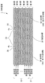
- FIG. 1 is a perspective view schematically showing an antenna device according to a first embodiment of the present invention.
- FIG. 2 is a cross-sectional view of the antenna device shown in FIG. 1 taken along the line AA. It is a dimension figure in the antenna device concerning a 1st embodiment. It is a perspective view in the other antenna device which concerns on 1st Embodiment. It is a figure showing the impedance characteristic in the 2.4 GHz band split ring resonator antenna which concerns on 2nd Embodiment. It is a figure showing the reflective characteristic in the 2.4 GHz band split ring resonator antenna which concerns on 2nd Embodiment.
- the strength at which a signal of a frequency of 5 GHz radiated from the 2.4 GHz band split ring resonator antenna according to the second embodiment leaks to the 5 GHz band split ring resonator antenna is determined with the 5 GHz band split ring resonator antenna. It is a figure showing the distance between antennas in the case of reducing by extending the space
- 2nd Embodiment it is a figure showing the impedance characteristic in a 2.4 GHz band split ring resonator antenna when the distance between antennas of a 2.4 GHz band and a 5 GHz band is shortened.
- the 2.4 GHz band signal leaked from the 2.4 GHz band split ring resonator antenna before the positions of the split portion and the feeder line are switched. It is a figure which represents typically the flow of the high frequency current which is.
- the signal is a 2.4 GHz band signal leaking from the 2.4 GHz band split ring resonator antenna after the positions of the split part and the feeder line of the 5 GHz band split ring resonator antenna are switched. It is a figure which represents typically the flow of a high frequency current.
- FIG. 1 is a perspective view schematically showing an antenna device according to the first embodiment of the present invention.
- the antenna device according to the present embodiment is roughly divided into a conductor substrate 1 in which a dielectric layer (not shown in FIG. 1) and a conductor layer (not shown in FIG. 1) are laminated.
- the 2.4 GHz band split ring resonator antenna 10 and the 5 GHz band split ring resonator antenna 20 formed on the conductor substrate 1 are provided.
- the 2.4 GHz band split ring resonator antenna 10 and the 5 GHz band split ring resonator antenna 20 are also abbreviated as “SR resonator antenna 10” and “SR resonator antenna 20”, respectively.
- the 2.4 GHz band SR resonator antenna 10 includes an opening 2a, a conductor via 3, a feeder line 4a, and a split portion 5a.
- the 5 GHz band SR resonator antenna 20 includes an opening 2b, a conductor via 3, a feeder line 4b, and a split portion 5b.
- a conductor layer having a substantially C shape (or C shape (hereinafter the same)) is formed around the openings 2a and 2b in order. That is, the substantially C-shaped conductor layer has a structure in which the portions indicated by the split portions 5a and 5b are cut out in order.
- Such a substantially C-shaped conductor layer is formed as a first split ring portion 31 and a second split ring portion 32, which will be described later, and is disposed so as to overlap each other.
- the openings 2a and 2b may be collectively referred to as “opening 2”.
- the SR resonator antennas 10 and 20 are formed on the conductor substrate 1 so that the sides where the split portions 5a and 5b are provided are exposed on the same end surface of the conductor substrate 1 in order.
- the split parts 5a and 5b may be collectively referred to as “split part 5”.
- the conductor via 3 is schematically shown as a gray grid in FIG. That is, the specific structure of the conductor via 3 is, for example, a cylindrical through hole as shown in FIG. Further, in the circumferential direction of the opening 2, adjacent to the conductor via 3, a portion schematically shown as a white grid shape represents the conductor substrate 1.
- FIG. 4 is a perspective view of another antenna device according to the first embodiment.
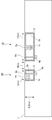
- FIG. 2 is a cross-sectional view of the antenna device shown in FIG. 1 taken along the line AA.
- the conductor substrate 1 includes a plurality of layers in which dielectric layers 35 and conductor layers 36 are alternately stacked as shown in FIG.
- the conductor substrate 1 includes a dielectric layer 35 and a conductor layer 36 in each layer from the first layer to the fifth layer as an example.
- the sixth layer extending along the fifth layer includes only the conductor layer 36.
- the conductor layer 36 that the first layer has as the outermost surface of the conductor substrate 1 is also referred to as a first conductor layer 36A for convenience of explanation.
- a first split ring portion 31a and a first split each having a substantially C-shape are formed on the first layer including the first conductor layer 36A and the dielectric layer 35, respectively.
- a ring portion 31b is formed.
- the first split ring portions 31a and 31b may be collectively referred to as “first split ring portion 31”.
- the second to fifth layers have a structure (structure) in which the second conductor layers 36B and the dielectric layers 35 are alternately stacked.
- the sixth layer is constituted by the first conductor layer.
- the second to fifth and sixth layers are formed with a second split ring part 32a and a second split ring part 32b, which are not shown in FIG. That is, in the schematic structural diagram shown in FIG. 1, the expression of the dielectric layers provided between the respective layers shown in FIG. 2 is omitted.
- the second split ring portions 32a and 32b may be collectively referred to as “second split ring portion 32”.
- the second split ring portion 32 will be described as an example having a total of five layers from the second layer to the sixth layer.
- the number of layers of the antenna device according to the present invention described using the present embodiment as an example is not limited to five layers.
- the sixth layer is a layer that constitutes a part of the second split ring portion 32 described above by the conductor layer 36 and wires (leads out) a feed line 4a and a feed line 4b described later.
- the feed lines 4a and 4b may be collectively referred to as “feed line 4” in the following description.
- the openings 2a and 2b shown in FIG. 1 represent a state schematically represented only by the conductor layer 36 by omitting the representation of the actually existing derivative layer 35 for convenience of explanation.
- the antenna device according to the present embodiment does not have a physically penetrating opening.
- each SR resonator antenna 10 and 20 will be further described.
- the 2.4 GHz band SR resonator antenna 10 includes a first split ring part 31a and a second split ring part 32a so as to overlap each other (FIG. 1).
- the split part 5a is a gap cut out in the opening 2a of the 2.4 GHz band SR resonator antenna 10.
- the split part 5a includes a first split part 51a corresponding to the first layer and a second split part 52a corresponding to the second to sixth layers.
- first split ring portion 31a and the second split ring portion 32a are formed so as to surround the opening 2a in a state of being cut out as shown in the first split portion 51a and the second split portion 52a in FIG. Yes.
- the first split ring portion 31a and the second split ring portion 32a have a structure in which the first layer and the second to sixth layers are stacked.
- the 5 GHz band SR resonator antenna 20 has the same configuration as the 2.4 GHz band SR resonator antenna 10 described above. That is, the 5 GHz band SR resonator antenna 20 is provided so that the first split ring part 31b and the second split ring part 32b are overlapped (FIG. 1).
- the split portion 5b is a gap cut out in the opening 2b of the 5 GHz band SR resonator antenna 20.
- the split part 5b includes a first split part 51b corresponding to the first layer and a second split part 52b corresponding to the second to sixth layers.
- first split ring part 31b and the second split ring part 32b are formed so as to surround the opening 2b in a state of being cut out as shown in the first split part 51b and the second split part 52b in FIG. Yes.
- the first split ring portion 31b and the second split ring portion 32b have a structure in which the first layer and the second to sixth layers are stacked.
- first split portions 51a and 51b in the SR resonator antennas 10 and 20 are collectively referred to as the first split portion 51, respectively.
- second split portions 52a and 52b in the SR resonator antennas 10 and 20 are sequentially referred to as the second split portion 52, respectively.
- the 2.4 GHz band SR resonator antenna 10 is referred to as a first split ring resonator antenna 10 that resonates in the 2.4 GHz band that is the first frequency.
- the 5 GHz band SR resonator antenna 20 is referred to as a second split ring resonator antenna 20 that resonates in the 5 GHz band that is the second frequency.
- the antenna device of this embodiment is a structure in which the dielectric layers 35 and the conductor layers are alternately stacked.
- This antenna device surrounds the opening 2 provided in the first conductor layer 36 ⁇ / b> A extending on the one surface side of the dielectric layer 35, and the first split portion 51 is formed on a part of the circumferential direction along the opening 2.
- the first split ring portion 31 is formed.
- the antenna device surrounds the opening 2 provided so as to face the first split ring portion 31 in the second conductor layer 36 ⁇ / b> B extending on the other surface side of the dielectric layer 35, and extends along the opening 2.
- a second split ring portion 32 having a second split portion 52 formed in a part in the circumferential direction is provided.
- a plurality of antenna devices are provided with a gap in the circumferential direction with the first split portion 51 and the second split portion 52 interposed therebetween, and a conductor that electrically connects the first split ring portion 31 and the second split ring portion 32. It has a via 3.
- the antenna device is provided in a specific conductor layer among the plurality of conductor layers, one end is electrically connected to at least one conductor via 3, and the other end is an extension of the specific conductor layer.
- the power supply line 4 is insulated from the specific conductor layer by a clearance 39 formed in the specific conductor layer.
- the antenna device of the present embodiment includes a plurality of the above-described structures, and constitutes the first split ring resonator antenna 10 that resonates at the first frequency by the first structure, and the second frequency by the second structure.
- a second split ring resonator antenna 20 that resonates at is configured.
- the antenna device includes the first split ring resonator antenna 10 that resonates at the first frequency and the second split ring resonator antenna 20 that resonates at the second frequency.
- the conductor via 3 is a conductor that electrically connects the conductor layer 36 in the first to sixth layers of the conductor substrate 1 and a feeding point 6 described later at a predetermined interval so as to surround the opening 2.
- the predetermined interval at which the conductor via 3 is provided is, for example, 1 mm (millimeter). However, the interval at which the conductor via 3 is provided is not limited to 1 mm.
- each of the power supply lines 4a and 4b is connected to a 2.4 GHz band and a 5 GHz band radio unit (high frequency circuit), not shown, respectively.
- feed point 6 The other ends of the feed lines 4a and 4b are connected to the feed point 6a and the feed point 6b (hereinafter also collectively referred to as “feed point 6”) in the SR resonator antennas 10 and 20, respectively.
- a high-frequency current is supplied / received to / from the radio unit in each frequency band.
- the feeding line 4 in the sixth layer and the other conductor layer 36 are electrically connected by at least one conductor via 3.
- the feeder line 4 is assumed to have a cross section perpendicular to the longitudinal direction of the feeder line 4 matched with the input / output impedance in the radio unit by having a rectangular conductor pattern, for example.
- a gap (clearance) is provided around the feeder lines 4a and 4b so as not to be short-circuited with the surrounding conductor layer 36 when connected to the above-described radio units.
- the clearance 39 is, for example, 0.5 mm.
- the clearance 39 provided around the feeder line 4 is not limited to 0.5 mm.
- the feeder 4 has been described as being drawn from the sixth layer in the second split ring portion 32 illustrated in FIG.
- the method of drawing out the feeder line 4 is not limited to the above-described method, and, for example, from the conductor layer 36 (that is, the first conductor layer 36A) on the outermost surface of the first split ring portion 31 (ie, the first conductor layer 36A) You may pull it out.
- the feeder line 4 forms a feeder line using the conductor layer 36 in at least one of the inner layers (that is, the second to fifth layers) in the second split ring portion 32. You may make it pull out.
- FIG. 4 is a perspective view of another antenna device according to the first embodiment.
- FIG. 4 shows the 2.4 GHz band SR resonator antenna 10 formed on the conductor substrate 1 for convenience of explanation only by the conductor layer provided with the split ring portion 12a and the feed line 4a. For this reason, in FIG. 4, the dielectric layer and the 5 GHz band SR resonator antenna 20 are not shown in FIG.
- the material of the conductor layer 36 forming a part of the conductor substrate 1 shown in FIG. 1 includes a conductive metal pattern such as a copper foil pattern, for example.
- the material of the dielectric layer 35 forming a part of the conductor substrate 1 shown in FIG. 1 is, for example, a glass epoxy substrate used for a printed board.
- the material of the dielectric layer 35 is not limited to this, and may be a ceramic substrate or the like.
- the SR resonator antennas 10 and 20 resonate in the respective frequency bands described above depending on the length of the conductor surrounding the outer periphery of each opening 2 and the electrostatic capacity between counter electrodes 7 (to be described later) sandwiching the split portion 5. .
- the SR resonator antennas 10 and 20 have opposed (paired) electrodes 7a and 7b provided at right angles from the opening ends of the split portions 5a and 5b toward the opening 2 in the split portions 5a and 5b, respectively.
- opposed (paired) electrodes 7a and 7b provided at right angles from the opening ends of the split portions 5a and 5b toward the opening 2 in the split portions 5a and 5b, respectively.
- counter electrode 7a and counter electrode 7b are also collectively referred to as “counter electrode 7”.
- the counter electrode 7 is provided to obtain the capacitance C in the split portions 5a and 5b.
- the capacitance C is the total area S of the surfaces where the conductor layers 36 constituting the counter electrode 7 sandwiching the split portion 5 face each other, the distance d between the counter electrodes 7, and the dielectric that the gap between the counter electrodes 7 has.
- the rate ⁇ (epsilon) is obtained based on the following known formula:
- the area S is a surface facing each other across the split portion 5 of the conductor layer 36 included in the counter electrode 7 of each antenna.
- the area S is the product of the total thickness (height) of each conductor layer 36 and the length of the counter electrode 7 provided at a right angle from the opening end of the split portion 5 toward the opening 2.
- the capacitance between the conductor layers 36 of different layers in the counter electrode 7 is negligible compared to the capacitance of the conductor layers 36 of the same layer facing each other across the split portion 5.
- the total height of the conductor layers in the counter electrode 7 is, for example, 0.8 mm in the case of a total of 6 layers. Further, the length of the counter electrode 7 is, for example, 3.5 mm and 2.5 mm in the SR resonator antennas 10 and 20, respectively. However, the dimension mentioned above is an example and is not limited to these dimensions.
- the number of conductor layers 36 constituting the counter electrode 7 sandwiching the split portion 5 of each antenna is not limited to six layers as long as a predetermined capacitance can be obtained between the counter electrodes 7. There may be.
- the 2.4 GHz band SR resonator antenna 10 has, as an example, conductor layers 36 that constitute counter electrodes in all six layers.
- the conductor layer 36 is provided only in the first layer and the sixth layer, and the counter electrode is not provided in the other conductor layers.
- providing a plurality of conductor layers 36 constituting the counter electrode 7 of each antenna can be regarded as a combined capacitance in which the capacitance between the counter electrodes of each conductor layer 36 is connected in parallel. And according to this embodiment, it becomes possible to adjust the electrostatic capacitance according to the number of layers of the conductor layer 36 constituting the counter electrode 7.
- the conductor via 3 that conducts between the conductor layers 36 is not provided other than the feeding point 6.
- the conductor via 3 may be appropriately provided in the counter electrode 7 sandwiching the split portion 5.
- the 2.4 GHz band SR resonator antenna 10 and the 5 GHz band SR resonator antenna 20 are based on the following equation that is known from the above-described capacitance C between the counter electrodes 7 and the inductive reactance L: Resonance occurs at frequencies f of 2.4 GHz band and 5 GHz band, respectively.
- the inductive reactance L is an impedance due to the line length which is the length of the conductor in the conductor layer 36 surrounding the outer periphery of the opening 2.
- the capacitance C is also referred to as “capacitive reactance” in the following description.
- the capacitive reactance C between the counter electrodes 7 can be increased by the following method using Equation 1. For example, a) By increasing the length of the counter electrode 7, the total area S of the surfaces where the conductor layers 36 constituting the counter electrode 7 face each other is increased.
- the capacitive reactance C in the SR resonator antennas 10 and 20 according to this embodiment can be increased by any one of these a) to c) or a combination of at least two of them.
- the capacitive reactance C can be adjusted by the thickness (height) of the conductor layer 36 as shown in Expression 1 in addition to the above-described elements.
- ⁇ (pi) in Equation 2 represents the circumference ratio.
- FIG. 3 is a dimensional diagram of the antenna device according to the first embodiment.
- the length of the side where the split portion 5 is provided is, for example, 13 mm for the 2.4 GHz band SR resonator antenna 10 and 5 mm for the 5 GHz band SR resonator antenna 20.
- the length in the depth direction from the end face where the split part 5 of the SR resonator antennas 10 and 20 is provided to the opening 2 is 4.5 mm, for example.
- the interval between the two SR resonator antennas is 4 mm, for example.
- the length (thickness) in the thickness direction (not shown) of the conductor substrate 1 depends on the number of layers of the conductor substrate 1.
- the thickness of the conductor substrate 1 is 1.6 mm as an example.
- the SR resonator antennas 10 and 20 described above are designed so as to resonate at the respective resonance frequencies when the respective SR resonator antennas 10 and 20 are independent.
- the positional relationship between the two SR resonator antennas 10 and 20 is interchanged, so that the 2.4 GHz band SR resonator antenna 10 and the 5 GHz band SR resonator antenna 20 are switched to the left and right shown in FIG. May be.
- an arrangement in which the positions of the feed line 4a and the split part 5a in the 2.4 GHz band SR resonator antenna 10 and the positions of the feed line 4b and the split part 5b in the 5 GHz band SR resonator antenna 20 are interchanged. It may be adopted.
- the present embodiment is not limited to the SR resonator antenna having the above-described shape, and may have other shapes as long as the SR resonator is formed.
- This embodiment has an effect that an antenna device using a split ring resonator can be realized using a multilayer printed board.
- FIG. 5A and FIG. 5B, and FIG. 6A and FIG. 6B are diagrams representing the antenna performance of the 2.4 GHz band SR resonator antenna 10 and the 5 GHz band SR resonator antenna 20 in order.
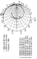
- FIG. 5A is a diagram illustrating impedance characteristics of the 2.4 GHz band SR resonator antenna 10 according to the second embodiment.
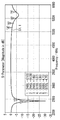
- FIG. 5B is a diagram illustrating the reflection characteristics in the 2.4 GHz band SR resonator antenna 10 according to the second embodiment.
- FIG. 6A is a diagram illustrating impedance characteristics in the 5 GHz band SR resonator antenna 20 according to the second embodiment.
- FIG. 6B is a diagram illustrating reflection characteristics in the 5 GHz band SR resonator antenna 20 according to the second embodiment.
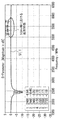
- the impedance characteristic represents what impedance (the real part and the imaginary part of the impedance characteristic) the SR resonator antennas 10 and 20 have. That is, the horizontal axis (horizontal line) of the circles shown in FIGS. 5A and 6A represents the pure resistance (the real part of the impedance characteristics) in the SR resonator antennas 10 and 20.
- the center point of the horizontal line represents 1 which is a numerical value normalized by 50 ⁇ . Then, with the numerical value 1 at the center point of the horizontal line as a reference, the left end represents 0 ⁇ (ohms) (that is, short circuit), and the right end represents ⁇ (infinite) ⁇ (that is, open).
- the line (circle) perpendicular to the horizontal line representing the real part represents the imaginary part (reactance component).
- the impedance characteristics of the SR resonator antenna are expressed in the semicircular part above the horizontal line in the following cases with reference to the numerical value 1 at the center point. That is, the next case is a case where an inductive reactance component such as a line pattern in the split ring portions 31 and 32 is added in series with the SR resonator antenna.
- the impedance characteristic of the SR resonator antenna is expressed in a semicircular portion below the horizontal line in the following case with the numerical value 1 at the center point as a reference. That is, the next case is a case where a capacitive reactance component such as the counter electrode 7 sandwiching the split portion 5 is added in series with the SR resonator antenna.
- the first numerical value represents the frequency value
- the following parentheses indicate the frequency value.
- the values of the real part and imaginary part of the impedance characteristic are expressed in order with a comma in between. That is, it represents that the real part of the impedance characteristic is 1.95 ohms and the value of the imaginary part is 51 ohms at a frequency of 2 GHz. That is, the description “Frequency / MHz” in FIG. 5A indicates that the unit of frequency is megahertz.
- each frequency shown in items 1 to 7 described in the lower left in FIG. 5A each frequency shown in items 1 to 3 represents a numerical value representing an impedance characteristic at a frequency in the 2.4 GHz band.
- Each frequency shown in items 4 to 7 indicates a numerical value representing impedance characteristics at a frequency of 5 GHz band.
- the way of viewing FIG. 5A is the same for FIGS. 6A and 10A.
- the impedance characteristics of the 2.4 GHz band SR resonator antenna 10 shown in FIG. 5A and the 5 GHz band SR resonator antenna 20 shown in FIG. 6A satisfy the impedance characteristics in the respective frequency bands. That is, FIG. 5A has a reactance component near the center frequency of the 2.4 GHz band in the vicinity of the numerical value 1 at the center point. Similarly, FIG. 6A has a reactance component near the center frequency of the 5 GHz band in the vicinity of the numerical value 1 at the center point.
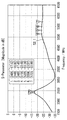
- the reflection characteristics shown in FIGS. 5B and 6B are such that when signals are input from the feed lines 4 of the SR resonator antennas 10 and 20, the input signals are reflected by the respective antennas and returned to the feed lines 4. Represents the incoming ratio
- the horizontal axis represents frequency
- the vertical axis represents the ratio of output (reflected) power to input power in dB (decibel).
- the horizontal axis representing the frequency shown in FIGS. 5B and 6B has a higher frequency in the right direction, and the vertical axis representing the reflectance has a lower reflection in the lower direction (that is, it is efficiently radiated). It represents.
- the reflection characteristics of the 2.4 GHz band SR resonator antenna 10 shown in FIG. 5B and the 5 GHz band SR resonator antenna 20 shown in FIG. 6B indicate that the reflection characteristics in the respective frequency bands are satisfied. That is, in FIG. 5B, reflection near the center frequency of the 2.4 GHz band is reduced. Further, in FIG. 6B, reflection near the center frequency of the 5 GHz band is reduced.
- the ratio of reflection (return loss value) at the frequency of the 5 GHz band other than the 2.4 GHz band of the center frequency of the 2.4 GHz band SR resonator antenna 10 shown in FIG. 5B is about ⁇ 7 dB.
- the 2.4 GHz band SR resonator antenna 10 has a characteristic of radiating (leaking) an input signal even in a frequency of 5 GHz band, which is a frequency other than the target frequency of 2.4 GHz band. .
- the 2.4 GHz band SR resonator antenna 10 has a characteristic of radiating even at a frequency of 5 GHz band. Conversely, the 2.4 GHz band SR resonator antenna 10 can easily receive a signal of a frequency of 5 GHz band. Means.
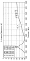
- FIG. 7 shows a signal output from the feed line 4b of the 5 GHz band SR resonator antenna 20 when a signal is input from the feed line 4a of the 2.4 GHz band SR resonator antenna 10 in the second embodiment. It is a figure showing the isolation characteristic which shows the ratio of the output electric power with respect to input electric power.
- Isolation characteristics are characteristics that represent the degree of signal separation between different inputs and outputs. That is, in FIG. 3, when a signal having a frequency of, for example, 2 GHz to 6 GHz is input to the power supply line 4a while changing the frequency, the signal at the frequency is output to the power supply line 4b. The ratio of the output power in the feed line 4b to the input power in the feed line 4a is expressed in dB.
- the horizontal axis represents frequency and the vertical axis represents isolation (degree of separation).
- the right direction represents that the frequency is high.
- the vertical axis representing the isolation indicates that the signal at that frequency is less leaked (ie, separated) to other SR resonator antennas.
- a signal input from the feed line 4a of the 2.4 GHz band SR resonator antenna 10 wraps around the 5 GHz band SR resonator antenna 20 and is output from the feed line 4b at an input power at a frequency of 5 GHz band.
- the ratio of the output power to the maximum value represents about -11 dB. That is, the signal of the frequency of 5 GHz band input to the feeder line 4a is output from the feeder line 4b with only about 11 dB attenuated.
- the SR resonator antennas 10 and 20 have reversibility in which the radiation characteristics when transmitting radio waves are the same as other antennas, that is, the reception characteristics when receiving radio waves. Thereby, the power of the signal of the frequency of the 5 GHz band input to the feeder line 4b is output from the feeder line 4a with only about 11 dB attenuated.
- the 2.4 GHz band SR resonator antenna 10 also receives a signal of a 5 GHz band frequency radiated from the 5 GHz band SR resonator antenna 20, thereby causing a high frequency of a 2.4 GHz band radio unit (not shown).
- the receiver circuit is saturated.
- the 2.4 GHz band radio unit (not shown) cannot receive a signal that should originally be received.
- the 2.4 GHz band SR resonator antenna 10 is As an antenna that receives a frequency of 5 GHz band, it does not operate.
- the high-frequency receiving circuit of the 2.4 GHz band radio unit is not saturated by the signal of the 5 GHz band frequency radiated from the 5 GHz band SR resonator antenna 20 (that is, the isolation characteristic is improved). Therefore, the 2.4 GHz band radio unit can receive signals that the 2.4 GHz band radio unit should originally receive.
- the isolation characteristic at a frequency of 5 GHz band depends on the design of a high-frequency circuit including a filter circuit and the like in each radio unit.
- the isolation characteristic value representing the degree of separation from the 2.4 GHz band SR resonator antenna 10 to the 5 GHz band SR resonator antenna 20 needs to ensure 20 dB, for example, There is a need to improve 9 dB from about 11 dB.
- 2.4 GHz band SR resonator antenna 10 and 5 GHz band SR resonator antenna 20 are used. It is necessary to widen the antenna interval.
- an antenna interval to be widened is required to be, for example, a 24 mm interval shown in FIG.
- Figure 8 shows the antenna shape and layout dimensions based on the simulation results.
- FIG. 8 shows the intensity of leakage of a signal of 5 GHz band frequency radiated from the 2.4 GHz band SR resonator antenna 10 according to the second embodiment to the 5 GHz band SR resonator antenna 20, in the 5 GHz band SR resonance. It is a figure showing the distance between antennas in the case of reducing by expanding the space
- FIG. 8 shows the intensity of leakage of a signal of 5 GHz band frequency radiated from the 2.4 GHz band SR resonator antenna 10 according to the second embodiment to the 5 GHz band SR resonator antenna 20, in the 5 GHz band SR resonance. It is a figure showing the distance between antennas in the case of reducing by expanding the space
- the ratio of the output power from the power supply line 4b to the input power of the 5 GHz band frequency signal input from the power supply line 4a satisfies the target 20 dB isolation characteristic value.
- the shape of the 5 GHz band SR resonator antenna 20 is not changed, and the 2.4 GHz band SR resonator is improved when the return loss value at the frequency of 5 GHz band in the 2.4 GHz band SR resonator antenna 10 is improved.
- the shape and arrangement on the antenna 10 side are changed.
- the 2.4 GHz band SR resonator antenna 10 and the 5 GHz band SR resonator antenna 20 are arranged close to each other, predetermined impedance characteristics in the respective SR resonator antennas 10 and 20, and The shape and arrangement of the SR resonator antenna 10 are adjusted so as to satisfy the reflection characteristics.
- FIG. 9 shows a dimensional diagram as a result of changing the shape and arrangement of the 2.4 GHz band SR resonator antenna 10.
- 10A and 10B show impedance characteristics and reflection characteristics of the 2.4 GHz band SR resonator antenna 10 in a state where the shape and arrangement of the 2.4 GHz band SR resonator antenna 10 are changed.
- FIG. 9 shows the size of the 2.4 GHz band SR resonator antenna 10 by adjusting the line length of the 2.4 GHz band SR resonator antenna 10 according to the second embodiment and the counter electrode 7 sandwiching the split part 5.
- FIG. 9 is a diagram for explaining a state in which the signal leakage at the frequency of 5 GHz band is reduced and the distance between the antennas in the 2.4 GHz band and the 5 GHz band is shortened.
- FIG. 10A illustrates the 2.4 GHz band SR resonator antenna 10 by adjusting the line length of the 2.4 GHz band SR resonator antenna 10 according to the second embodiment and the counter electrode 7 sandwiching the split portion 5. It is a figure showing the impedance characteristic figure at the time of reducing size. Further, FIG. 10A shows that in the 2.4 GHz band SR resonator antenna 10 when the signal leakage at the frequency of 5 GHz band is reduced and the distance between the antennas of the 2.4 GHz band and the 5 GHz band is shortened. It is also a figure showing an impedance characteristic diagram.
- FIG. 10B shows the 2.4 GHz band SR resonator antenna 10 by adjusting the line length of the 2.4 GHz band SR resonator antenna 10 according to the second embodiment and the counter electrode 7 sandwiching the split part 5. It is a figure showing the reflective characteristic at the time of reducing size.
- FIG. 10B also shows that the 2.4 GHz band SR resonator antenna 10 when the signal leakage at the frequency of the 5 GHz band is reduced and the distance between the antennas of the 2.4 GHz band and the 5 GHz band is shortened. It is a figure showing the reflective characteristic in.
- the 2.4 GHz band SR resonator antenna is set so that the ratio of the reflected power to the input power representing the reflection characteristics in the frequency of the 5 GHz band approaches zero. Adjustment to reduce the size of 10 is performed.
- the antenna device design method considers a case where the 2.4 GHz band SR resonator antenna 10 has reflected power with respect to input power at a frequency of 5 GHz band.
- the line length which is the length of the conductor surrounding the outer periphery of the opening 2a, which is a component of the inductive reactance L in the 2.4 GHz band SR resonator antenna 10, is shortened.
- the design method of the present antenna device is that the resonance frequency f remains at the center frequency of the 2.4 GHz band, and the capacitance between the counter electrodes 7 in the 2.4 GHz band SR resonator antenna 10 is calculated according to Equation 2. (In other words, the capacitive reactance C) can be increased.
- the method of increasing the capacitive reactance C can be increased by the following method using Equation 1. That is, a) Increasing the length of the counter electrode 7 in the 2.4 GHz band SR resonator antenna 10 increases the area S of the surface where the conductor layers 36 constituting the counter electrode 7 face each other.
- the capacitive reactance C can be increased by any one of these a) to c) or a combination of at least two of them.
- the capacitive reactance C can be adjusted by the thickness (height) of the conductor layer 36 in addition to the elements described above.
- FIGS. 5A and 5B showing the antenna characteristics of the 2.4 GHz band SR resonator antenna 10 before adjusting the size of the 2.4 GHz band SR resonator antenna 10, and the above-described 2.4 GHz band SR resonator antenna 10.
- FIG. 10A and FIG. 10B showing antenna characteristics after adjusting the size of 10 are compared.
- the return loss value of the frequency of 5 GHz band is improved from about ⁇ 7 dB to 0 dB.
- a signal with a frequency of 5 GHz band input from the feed line 4 b in the 5 GHz band SR resonator antenna 20 does not leak to the feed line 4 a in the 2.4 GHz band SR resonator antenna 10.
- the 2.4 GHz band SR resonator antenna 10 has a length of the side where the split portion 5a is provided and the length of the side facing the side shown in FIG. It is shortened to 9 mm.
- FIG. 11 shows the isolation characteristics of the SR resonator antennas 10 and 20 shown in FIG.
- FIG. 11 shows that the signal length at the frequency of 5 GHz band is reduced by adjusting the line length of the 2.4 GHz band SR resonator antenna 10 according to the second embodiment and the counter electrode 7 sandwiching the split part 5. It is a figure showing an isolation characteristic. Further, FIG. 11 shows the 5 GHz band SR resonance when a signal is input from the feeder line 4 a of the 2.4 GHz band SR resonator antenna 10 when the distance between the antennas of the 2.4 GHz band and the 5 GHz band is shortened. It is also a figure showing the isolation characteristic which shows the ratio of the output electric power with respect to input electric power of the signal output from the feeder line 4b of the antenna unit 20.
- the return loss in the 2.4 GHz band SR resonator antenna 10 was improved. As a result, it can be seen that isolation is ensured even when the antenna interval between the SR resonator antennas 10 and 20 is as narrow as 4 mm as shown in FIG. 3, as shown in FIG. That is, in FIG. 11, the signal of the frequency of 5 GHz band from the 2.4 GHz band SR resonator antenna 10 to the 5 GHz band SR resonator antenna 20 is reduced by 20 dB or more.
- This embodiment has an effect of reducing the signal leakage from the SR resonator antenna that resonates in the higher frequency band to the SR resonator antenna that resonates in the lower frequency band. This effect can be realized without adding components or the like even when split ring resonator antennas corresponding to different frequency bands are arranged close to each other.
- the reflection characteristic (return loss value) of the higher frequency in the antenna in the lower frequency band affected by the antenna in the higher frequency band Is adjusted to approach zero.
- This embodiment is different in that the positions of the feeder line 4b and the split part 5b in the 5 GHz band SR resonator antenna 20 of the first and second embodiments are interchanged.
- the isolation in the 2.4 GHz band is about ⁇ 17 dB.
- the isolation characteristic is about 3 dB short of the target of ⁇ 20 dB.
- the positions of the feed line 4b and the split part 5b of the 5 GHz band SR resonator antenna 20 are switched as shown in FIG. 12B from the configuration in FIG. 9 (or FIG. 12A).
- FIG. 12A shows the leakage from the 2.4 GHz band SR resonator antenna 10 before switching the positions of the split part 5b and the feeder line 4b in the 5 GHz band SR resonator antenna 20 according to the third embodiment of the present invention. It is a figure which represents typically the flow of the high frequency current which is a signal of .4 GHz band.
- FIG. 12B shows the leakage from the 2.4 GHz band SR resonator antenna 10 after the positions of the split part 5b and the feed line 4b of the 5 GHz band SR resonator antenna 20 according to the third embodiment are switched. It is a figure which represents typically the flow of the high frequency electric current which is a 4 GHz band signal. This is a configuration for improving the isolation characteristic of the 2.4 GHz band SR resonator antenna 10 to the 5 GHz band SR resonator antenna in the present embodiment.
- FIG. 12A shows a case where the feed line 4b of the 5 GHz band SR resonator antenna 20 is on the side close to the 2.4 GHz band SR resonator antenna 10.
- a 2.4 GHz-band frequency signal input from the feed line 4a of the 2.4 GHz band SR resonator antenna 10 slightly enters the feed line 4b of the 5 GHz band antenna through a path indicated by a dotted arrow.
- the 5 GHz band SR resonator antenna 20 receives the 2.4 GHz band frequency signal radiated from the 2.4 GHz band SR resonator antenna 10, so that the high frequency receiving circuit of the radio section of the 5 GHz band can be obtained. Saturates. Thus, the 5 GHz band SR resonator antenna 20 cannot receive a signal that the 5 GHz band radio unit should originally receive.
- FIG. 12B the case where the feeder line 4b and these positions are switched so that the slit portion 5b is disposed on the side close to the 2.4 GHz band SR resonator antenna 10 in the 5 GHz band SR resonator antenna 20.
- a 2.4 GHz band frequency signal input from the feeder line 4a of the 2.4 GHz band SR resonator antenna 10 enters the 5 GHz band SR resonator antenna 20, it bypasses the split portion 5b and is shown by a dotted arrow. Attenuated by the detour path indicated by, and enters the feeder line 4b.
- the slit portion 5b is adjusted so as to resonate at a frequency of 5 GHz band, and therefore the capacitance is small for a signal of a frequency of 2.4 GHz band. Therefore, when viewed from the 2.4 GHz band frequency signal output from the 2.4 GHz band SR resonator antenna 10, it is difficult to pass through the slit section 5b because the slit section 5b is open. On the other hand, a 2.4 GHz band frequency signal passes through the detour path schematically shown by the dotted arrow in FIG. 12B, which is easier to pass than the slit portion 5b.
- FIG. 13 shows the isolation characteristics of the SR resonator antenna having the configuration shown in FIG. 12B.
- FIG. 13 is a plan view of the split portion 5b of the 5 GHz band SR resonator antenna 20 in order to improve the isolation characteristics in the 2.4 GHz band frequency of the 2.4 GHz band SR resonator antenna 10 according to the third embodiment. It is a figure showing the characteristic at the time of exchanging a position with electric wire 4b. FIG. 13 shows an input of a signal output from the feed line 4b of the 5 GHz band SR resonator antenna 20 when a signal is input from the feed line 4a of the 2.4 GHz band SR resonator antenna 10 in that case. It is also a figure showing the isolation characteristic showing the ratio of output electric power to electric power.
- FIG. 11 showing the isolation characteristics in the SR resonator antenna shown in FIG. 9 described in the second embodiment before switching the positions of the feeder line 4b and the split part 5b in the 5 GHz band SR resonator antenna 20;
- the isolation characteristic at the frequency in the 2.4 GHz band is improved by about 5 dB from about ⁇ 17 dB before improvement to about ⁇ 22 dB after improvement, and satisfies the target of 20 dB.
Landscapes
- Engineering & Computer Science (AREA)
- Computer Hardware Design (AREA)
- Physics & Mathematics (AREA)
- Theoretical Computer Science (AREA)
- General Physics & Mathematics (AREA)
- General Engineering & Computer Science (AREA)
- Geometry (AREA)
- Evolutionary Computation (AREA)
- Details Of Aerials (AREA)
- Architecture (AREA)
- Software Systems (AREA)
- Waveguide Aerials (AREA)
- Variable-Direction Aerials And Aerial Arrays (AREA)
- Aerials With Secondary Devices (AREA)
Abstract
Description
誘電体層と、導体層とが交互に積層された構造体に、
該誘電体層の一面側に延設された第1の導体層に設けられた、開口を囲むとともに、その開口に沿う周方向の一部に第1スプリット部が形成された第1スプリットリング部と、
前記誘電体層の他面側に延設された第2の導体層に、前記第1スプリットリング部と対向するように設けられた開口を囲むとともに、その開口に沿う周方向の一部に第2スプリット部が形成された第2スプリットリング部と、
前記第1スプリット部及び前記第2スプリット部を挟み、周方向に間隔を隔てて複数設けられ、前記第1スプリットリング部と前記第2スプリットリング部とを電気的に接続する導体ビアと、
前記複数の導体層のうち、特定の導体層に設けられ、一端が、少なくとも一つの前記導体ビアに電気的に接続され、他端が、該特定の導体層の延設方向に沿って、該特定の導体層に形成されたクリアランスによって該特定の導体層と絶縁された給電線と、
を含む構造を複数備え、
第1の前記構造によって第1の周波数で共振する第1スプリットリング共振器アンテナを構成し、第2の前記構造によって第2の周波数で共振する第2スプリットリング共振器アンテナを構成する。
アンテナ装置を、
第1スプリットリング共振器アンテナへ入力される第2の周波数の信号の入力電力に対する、該入力された第2の周波数の信号が前記第1スプリットリング共振器アンテナから反射される際の出力電力の比率を表す反射率の値を零に近づけるように、前記第1スプリットリング共振器アンテナにおける第1及び第2スプリット部が設けられた辺及びその辺に対向する辺の長さを短縮するのに応じて、前記第1スプリットリング共振器アンテナにおける対向電極間が有する静電容量を増大させるように調整する。
図1は、本発明の第1の実施形態に係るアンテナ装置を模式的に示す斜視図である。
しかし、本実施形態を例に説明する本発明に係るアンテナ装置の層数は、5層に限定されない。
面積Sは、上記のとおり、各アンテナの対向電極7が有する導体層36のスプリット部5を挟んで対向し合う面である。係る面積Sは、各導体層36の厚み(高さ)の合計と、スプリット部5の開口端部から開口部2に向って直角に設けられた対向電極7の長さとの積である。尚、ここでは、対向電極7における異なる層の導体層36間の静電容量は、スプリット部5を挟んで向き合う同じ層の導体層36同士の静電容量に比べて無視しうるものとする。
ここで、例えばSR共振器アンテナのサイズを小さくしたい場合は、誘導性リアクタンスLである開口部2の外周を囲む導体の長さである線路長を短くする。しかし、共振周波数fは、目的とする上述した周波数帯で一定とする必要があるので、式2により、対向電極7間の容量性リアクタンスCは、増やす必要がある。
a)対向電極7の長さを長くすることで対向電極7を成す各導体層36同士が向き合う面の合計面積Sを増やす。
第1の実施形態を基本とする第2の実施形態について、図5乃至図11を参照して説明する。
a)2.4GHz帯SR共振器アンテナ10における対向電極7の長さを長くすることで対向電極7を成す各導体層36同士が向き合う面の面積Sを増やす。
第1及び第2の実施形態を基本とする第3の実施形態について、図12A、図12B、及び図13を用いて説明する。
2、2a、2b 開口
3 導体ビア
4、4a、4b 給電線
5、5a、5b スプリット部
6、6a、6b 給電点
7、7a、7b 対向電極
10 2.4GHz帯SR共振器アンテナ
12a スプリットリング部
20 5GHz帯SR共振器アンテナ
31、31a、31b 第1スプリットリング部
32、32a、32b 第2スプリットリング部
35 誘電体層
36 導体層
36A 第1の導体層
36B 第2の導体層
39 クリアランス
51、51a、51b 第1スプリット部
52、52a、52b 第2スプリット部
Claims (9)
- 誘電体層と、導体層とが交互に積層された構造体に、該誘電体層の一面側に延設された第1の導体層に設けられた、開口を囲むとともに、その開口に沿う周方向の一部に第1スプリット部が形成された第1スプリットリング部と、
前記誘電体層の他面側に延設された第2の導体層に、前記第1スプリットリング部と対向するように設けられた開口を囲むとともに、その開口に沿う周方向の一部に第2スプリット部が形成された第2スプリットリング部と、
前記第1スプリット部及び前記第2スプリット部を挟み、周方向に間隔を隔てて複数設けられ、前記第1スプリットリング部と前記第2スプリットリング部とを電気的に接続する導体ビアと、
前記複数の導体層のうち、特定の導体層に設けられ、一端が、少なくとも一つの前記導体ビアに電気的に接続され、他端が、該特定の導体層の延設方向に沿って、該特定の導体層に形成されたクリアランスによって該特定の導体層と絶縁された給電線と、
を含む構造を複数備え、
第1の前記構造によって第1の周波数で共振する第1スプリットリング共振器アンテナを構成し、第2の前記構造によって第2の周波数で共振する第2スプリットリング共振器アンテナを構成することを特徴とするアンテナ装置。 - 前記第1及び第2スプリットリング共振器アンテナがそれぞれ有する前記第2スプリットリング部が、複数の前記誘電体層を挟む複数の前記第2の導体層と、前記第2スプリットリング部と接する前記第1スプリットリング部とは反対側の前記第2スプリットリング部における、最外の前記第2の導体層に設けられた前記給電線とから成ることを特徴とする請求項1に記載のアンテナ装置。
- 前記第1及び第2スプリットリング共振器アンテナがそれぞれ有する前記第1及び第2スプリット部が設けられた辺が、前記構造体の一端面に露出するように形成されることを特徴とする請求項1または請求項2に記載のアンテナ装置。
- 前記第1及び第2スプリットリング共振器アンテナがそれぞれ有する前記第1及び第2スプリット部を挟むように、前記第1及び第2スプリットリング部の両端の前記各導体層から、それぞれ前記開口が設けられた内側方向へ直角に設けられた対向電極を設けたことを特徴とする請求項1乃至請求項3の何れか1項に記載のアンテナ装置。
- 前記第1の周波数は、2.4GHz帯の周波数であり、前記第2の周波数は、5GHz帯の周波数であることを特徴とする請求項1に記載のアンテナ装置。
- 請求項1乃至5の何れかに記載したアンテナ装置を、
第1スプリットリング共振器アンテナへ入力される第2の周波数の信号の入力電力に対する、該入力された第2の周波数の信号が前記第1スプリットリング共振器アンテナから反射される際の出力電力の比率を表す反射率の値を零に近づけるように、前記第1スプリットリング共振器アンテナにおける第1及び第2スプリット部が設けられた辺及びその辺に対向する辺の長さを短縮するのに応じて、前記第1スプリットリング共振器アンテナにおける対向電極間が有する静電容量を増大させるように調整する、
ことを特徴とするアンテナ装置設計方法。 - 前記第1スプリットリング共振器アンテナにおける前記第1及び第2スプリット部が設けられた辺およびその辺に対向する辺の長さを短縮するのに応じて、前記対向電極の長さを長くするか、前記対向電極同士の間隙距離を短くするか、または、前記対向電極を成す導体層の層数を増やすかの何れか、又は、これらのうちの少なくとも2つの手順の組み合わせにより、前記対向電極間の静電容量を増大させる、
ことを特徴とする請求項6に記載のアンテナ装置設計方法。 - 前記第1スプリットリング共振器アンテナから放射される信号が前記第2スプリットリング共振器アンテナに漏洩する際の、前記第1スプリットリング共振器アンテナの前記給電線へ入力された前記信号の入力電力に対する、第2スプリットリング共振器アンテナの前記給電線から出力された前記漏洩した信号の出力電力の比率を表すアイソレーション特性を表す値を、前記第2スプリットリング共振器アンテナにおける前記スプリット部と前記給電線との位置を入れ替えることにより低減する、
ことを特徴とする請求項6又は請求項7の何れかに記載のアンテナ装置設計方法。 - 前記第1の周波数は、2.4GHz帯の周波数であり、前記第2の周波数は、5GHz帯の周波数である、
ことを特徴とする請求項6に記載のアンテナ装置設計方法。
Priority Applications (3)
| Application Number | Priority Date | Filing Date | Title |
|---|---|---|---|
| JP2015501318A JP6010213B2 (ja) | 2013-02-20 | 2014-02-13 | アンテナ装置およびその設計方法 |
| CN201480009690.5A CN105009365B (zh) | 2013-02-20 | 2014-02-13 | 天线装置及其设计方法 |
| US14/767,657 US9748641B2 (en) | 2013-02-20 | 2014-02-13 | Antenna device and method for designing same |
Applications Claiming Priority (2)
| Application Number | Priority Date | Filing Date | Title |
|---|---|---|---|
| JP2013-031233 | 2013-02-20 | ||
| JP2013031233 | 2013-02-20 |
Publications (1)
| Publication Number | Publication Date |
|---|---|
| WO2014129147A1 true WO2014129147A1 (ja) | 2014-08-28 |
Family
ID=51390947
Family Applications (1)
| Application Number | Title | Priority Date | Filing Date |
|---|---|---|---|
| PCT/JP2014/000729 Ceased WO2014129147A1 (ja) | 2013-02-20 | 2014-02-13 | アンテナ装置およびその設計方法 |
Country Status (4)
| Country | Link |
|---|---|
| US (1) | US9748641B2 (ja) |
| JP (1) | JP6010213B2 (ja) |
| CN (1) | CN105009365B (ja) |
| WO (1) | WO2014129147A1 (ja) |
Cited By (2)
| Publication number | Priority date | Publication date | Assignee | Title |
|---|---|---|---|---|
| CN106663864A (zh) * | 2014-12-22 | 2017-05-10 | 华为技术有限公司 | 一种天线和终端 |
| JP2017139685A (ja) * | 2016-02-05 | 2017-08-10 | Necプラットフォームズ株式会社 | アンテナ装置及び無線通信装置 |
Families Citing this family (7)
| Publication number | Priority date | Publication date | Assignee | Title |
|---|---|---|---|---|
| JP5725573B2 (ja) * | 2013-02-26 | 2015-05-27 | Necプラットフォームズ株式会社 | アンテナ及び電子装置 |
| JP5947263B2 (ja) * | 2013-08-27 | 2016-07-06 | Necプラットフォームズ株式会社 | アンテナおよび無線通信装置 |
| JP6763372B2 (ja) * | 2015-04-02 | 2020-09-30 | 日本電気株式会社 | マルチバンドアンテナ及び無線通信装置 |
| JP6659519B2 (ja) * | 2016-11-02 | 2020-03-04 | 株式会社東芝 | アンテナ装置 |
| TWI765743B (zh) * | 2021-06-11 | 2022-05-21 | 啓碁科技股份有限公司 | 天線結構 |
| CN113871839A (zh) * | 2021-09-27 | 2021-12-31 | 东莞华贝电子科技有限公司 | 一种终端设备 |
| US20250219669A1 (en) * | 2023-12-29 | 2025-07-03 | Google Llc | Computing Device Having Sensor with Integrated Antenna |
Citations (3)
| Publication number | Priority date | Publication date | Assignee | Title |
|---|---|---|---|---|
| JP2006217026A (ja) * | 2005-02-01 | 2006-08-17 | Hitachi Metals Ltd | アンテナ装置及びこれを用いた通信機器 |
| JP2006526322A (ja) * | 2003-05-09 | 2006-11-16 | コーニンクレッカ フィリップス エレクトロニクス エヌ ヴィ | ハウジングに組み込まれるアンテナ |
| JP2012244608A (ja) * | 2011-05-24 | 2012-12-10 | Lenovo Singapore Pte Ltd | 無線端末装置用のアンテナ |
Family Cites Families (8)
| Publication number | Priority date | Publication date | Assignee | Title |
|---|---|---|---|---|
| US4792809A (en) * | 1986-04-28 | 1988-12-20 | Sanders Associates, Inc. | Microstrip tee-fed slot antenna |
| JPH05315828A (ja) | 1992-05-07 | 1993-11-26 | Toyota Motor Corp | マイクロストリップアンテナ |
| JP3633593B2 (ja) * | 2002-07-24 | 2005-03-30 | 日本電気株式会社 | 高周波回路及び該高周波回路を用いたシールディドループ型磁界検出器 |
| KR101023903B1 (ko) * | 2008-09-17 | 2011-03-22 | 경기대학교 산학협력단 | 음의 유전율을 갖는 전자파 차폐 구조체 및 그 제조방법 |
| WO2011108341A1 (ja) | 2010-03-03 | 2011-09-09 | 株式会社村田製作所 | 無線通信デバイス及び無線通信端末 |
| TWI455404B (zh) * | 2010-11-02 | 2014-10-01 | Ind Tech Res Inst | 調節電磁波穿透響應的結構與調節電磁波輻射特性的天線結構 |
| CN103748741B (zh) * | 2011-08-24 | 2016-05-11 | 日本电气株式会社 | 天线和电子装置 |
| CN102354790B (zh) * | 2011-10-25 | 2014-04-09 | 电子科技大学 | 高度小型化的基片集成波导谐振器 |
-
2014
- 2014-02-13 US US14/767,657 patent/US9748641B2/en active Active
- 2014-02-13 WO PCT/JP2014/000729 patent/WO2014129147A1/ja not_active Ceased
- 2014-02-13 JP JP2015501318A patent/JP6010213B2/ja active Active
- 2014-02-13 CN CN201480009690.5A patent/CN105009365B/zh active Active
Patent Citations (3)
| Publication number | Priority date | Publication date | Assignee | Title |
|---|---|---|---|---|
| JP2006526322A (ja) * | 2003-05-09 | 2006-11-16 | コーニンクレッカ フィリップス エレクトロニクス エヌ ヴィ | ハウジングに組み込まれるアンテナ |
| JP2006217026A (ja) * | 2005-02-01 | 2006-08-17 | Hitachi Metals Ltd | アンテナ装置及びこれを用いた通信機器 |
| JP2012244608A (ja) * | 2011-05-24 | 2012-12-10 | Lenovo Singapore Pte Ltd | 無線端末装置用のアンテナ |
Non-Patent Citations (1)
| Title |
|---|
| HIROSHI TOYAO ET AL.: "Electrically Small Split-Ring Resonator Antenna", 2011 NEN IEICE COMMUNICATIONS SOCIETY CONFERENCE, THE INSTITUTE OF ELECTRONICS, INFORMATION AND COMMUNICATION ENGINEERS, vol. 133, 30 August 2011 (2011-08-30), pages B-1 - 133 * |
Cited By (4)
| Publication number | Priority date | Publication date | Assignee | Title |
|---|---|---|---|---|
| CN106663864A (zh) * | 2014-12-22 | 2017-05-10 | 华为技术有限公司 | 一种天线和终端 |
| EP3226349A4 (en) * | 2014-12-22 | 2017-11-15 | Huawei Technologies Co. Ltd. | Antenna and terminal |
| US10320068B2 (en) | 2014-12-22 | 2019-06-11 | Huawei Technologies Co., Ltd. | Antenna and terminal |
| JP2017139685A (ja) * | 2016-02-05 | 2017-08-10 | Necプラットフォームズ株式会社 | アンテナ装置及び無線通信装置 |
Also Published As
| Publication number | Publication date |
|---|---|
| US9748641B2 (en) | 2017-08-29 |
| US20150380810A1 (en) | 2015-12-31 |
| CN105009365A (zh) | 2015-10-28 |
| JPWO2014129147A1 (ja) | 2017-02-02 |
| JP6010213B2 (ja) | 2016-10-19 |
| CN105009365B (zh) | 2017-12-12 |
Similar Documents
| Publication | Publication Date | Title |
|---|---|---|
| JP6010213B2 (ja) | アンテナ装置およびその設計方法 | |
| US11387568B2 (en) | Millimeter-wave antenna array element, array antenna, and communications product | |
| JP6129857B2 (ja) | 偏波共用アンテナ | |
| JP6222103B2 (ja) | アンテナ及び無線通信装置 | |
| US9357633B2 (en) | Structure, wiring board, and method of manufacturing wiring board | |
| US20150364823A1 (en) | Antenna device and wireless device | |
| JP6775016B2 (ja) | 偏波共用平面超広帯域アンテナ | |
| US10476172B2 (en) | Antenna, antenna array, and wireless communication device | |
| JP5381463B2 (ja) | アンテナとそれを有する通信装置 | |
| US11658372B2 (en) | Transmission line and antenna | |
| WO2016021372A1 (ja) | アンテナ装置、及び、このアンテナ装置に備えられる表面電流抑制フィルタ | |
| CN107681275A (zh) | 天线及电子装置 | |
| WO2015049816A1 (ja) | アンテナ装置 | |
| JP5863730B2 (ja) | アンテナ装置及び無線通信装置 | |
| JP2015185910A (ja) | 通信装置及びアンテナ装置 | |
| JP6146801B2 (ja) | 配線基板、及び電子装置 | |
| JP2012147119A (ja) | 電磁結合器及びそれを搭載した情報通信機器 | |
| WO2021009893A1 (ja) | 周波数選択板 | |
| JP7077137B2 (ja) | 伝送線路およびコネクタ | |
| JPWO2011115094A1 (ja) | ノイズ抑制構造 | |
| WO2011122502A1 (ja) | ノイズ抑制構造 | |
| CN107896420A (zh) | 电路板及其电磁带隙结构 | |
| US9525213B2 (en) | Antenna device | |
| US9583812B2 (en) | Thin, flexible transmission line for band-pass signals | |
| US20260122767A1 (en) | Substrate connection structure, antenna substrate, and display device |
Legal Events
| Date | Code | Title | Description |
|---|---|---|---|
| 121 | Ep: the epo has been informed by wipo that ep was designated in this application |
Ref document number: 14754875 Country of ref document: EP Kind code of ref document: A1 |
|
| ENP | Entry into the national phase |
Ref document number: 2015501318 Country of ref document: JP Kind code of ref document: A |
|
| WWE | Wipo information: entry into national phase |
Ref document number: 14767657 Country of ref document: US |
|
| NENP | Non-entry into the national phase |
Ref country code: DE |
|
| 122 | Ep: pct application non-entry in european phase |
Ref document number: 14754875 Country of ref document: EP Kind code of ref document: A1 |