WO2014115277A1 - ストレージ装置およびストレージ装置制御方法 - Google Patents
ストレージ装置およびストレージ装置制御方法 Download PDFInfo
- Publication number
- WO2014115277A1 WO2014115277A1 PCT/JP2013/051392 JP2013051392W WO2014115277A1 WO 2014115277 A1 WO2014115277 A1 WO 2014115277A1 JP 2013051392 W JP2013051392 W JP 2013051392W WO 2014115277 A1 WO2014115277 A1 WO 2014115277A1
- Authority
- WO
- WIPO (PCT)
- Prior art keywords
- data
- crc
- code
- processor
- partial
- Prior art date
- Legal status (The legal status is an assumption and is not a legal conclusion. Google has not performed a legal analysis and makes no representation as to the accuracy of the status listed.)
- Ceased
Links
Images




Classifications
-
- G—PHYSICS
- G06—COMPUTING OR CALCULATING; COUNTING
- G06F—ELECTRIC DIGITAL DATA PROCESSING
- G06F11/00—Error detection; Error correction; Monitoring
- G06F11/07—Responding to the occurrence of a fault, e.g. fault tolerance
- G06F11/08—Error detection or correction by redundancy in data representation, e.g. by using checking codes
- G06F11/10—Adding special bits or symbols to the coded information, e.g. parity check, casting out 9's or 11's
- G06F11/1004—Adding special bits or symbols to the coded information, e.g. parity check, casting out 9's or 11's to protect a block of data words, e.g. CRC or checksum
-
- G—PHYSICS
- G06—COMPUTING OR CALCULATING; COUNTING
- G06F—ELECTRIC DIGITAL DATA PROCESSING
- G06F11/00—Error detection; Error correction; Monitoring
-
- G—PHYSICS
- G06—COMPUTING OR CALCULATING; COUNTING
- G06F—ELECTRIC DIGITAL DATA PROCESSING
- G06F11/00—Error detection; Error correction; Monitoring
- G06F11/07—Responding to the occurrence of a fault, e.g. fault tolerance
- G06F11/08—Error detection or correction by redundancy in data representation, e.g. by using checking codes
-
- G—PHYSICS
- G06—COMPUTING OR CALCULATING; COUNTING
- G06F—ELECTRIC DIGITAL DATA PROCESSING
- G06F11/00—Error detection; Error correction; Monitoring
- G06F11/07—Responding to the occurrence of a fault, e.g. fault tolerance
- G06F11/08—Error detection or correction by redundancy in data representation, e.g. by using checking codes
- G06F11/10—Adding special bits or symbols to the coded information, e.g. parity check, casting out 9's or 11's
- G06F11/1076—Parity data used in redundant arrays of independent storages, e.g. in RAID systems
- G06F11/1096—Parity calculation or recalculation after configuration or reconfiguration of the system
-
- G—PHYSICS
- G06—COMPUTING OR CALCULATING; COUNTING
- G06F—ELECTRIC DIGITAL DATA PROCESSING
- G06F13/00—Interconnection of, or transfer of information or other signals between, memories, input/output devices or central processing units
-
- G—PHYSICS
- G06—COMPUTING OR CALCULATING; COUNTING
- G06F—ELECTRIC DIGITAL DATA PROCESSING
- G06F13/00—Interconnection of, or transfer of information or other signals between, memories, input/output devices or central processing units
- G06F13/14—Handling requests for interconnection or transfer
- G06F13/20—Handling requests for interconnection or transfer for access to input/output bus
- G06F13/28—Handling requests for interconnection or transfer for access to input/output bus using burst mode transfer, e.g. direct memory access DMA, cycle steal
Definitions
- the present invention relates to a data guarantee technique in a storage apparatus.
- Patent Document 1 A technique for generating and confirming a guarantee code for transferred data in a communication interface between a storage apparatus and a host computer is known (Patent Document 1).
- the DMA controller calculates a guarantee code for the concatenated data.
- a certain DMA controller performs a certain data guarantee code calculation, and another DMA controller takes over the result of the calculation and transfers the next data.
- the guarantee code is calculated. In this case, even if a plurality of DMA controllers are used, it is difficult to improve the data transfer performance because it is necessary to sequentially calculate a plurality of data.
- a storage apparatus includes a channel control unit connected to a host computer, a storage unit connected to the channel control unit, the channel control unit, and the storage unit Connected to the processor.
- the channel control unit has a plurality of calculation units.
- the processor receives a request to read a plurality of element data from the host computer, the processor designates the plurality of element data for the plurality of arithmetic units, respectively.
- the plurality of arithmetic units respectively read the plurality of element data from the storage unit, calculate a plurality of partial codes that are a plurality of guarantee codes based on the plurality of element data, and send the plurality of parts to the processor. Send each code.
- the processor calculates a sequence code, which is a guarantee code of sequence data including the plurality of concatenated element data, based on the plurality of partial codes.
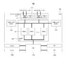
- FIG. 1 shows the configuration of a storage apparatus according to an embodiment of the present invention.
- FIG. 2 shows the configuration of the channel adapter 220.
- FIG. 3 shows an example of response data for a multitrack read request.
- FIG. 4 schematically shows the multitrack read process.
- FIG. 5 shows the DMA processing.
- FIG. 6 shows the final CRC process.
- FIG. 7 shows a specific example of CRC final processing.
- FIG. 8 shows the operation of the DMA controller and the MP 240 regarding CRC calculation.
- aaa table such as “aaa list”, “aaaDB”, “aaa queue”, etc.
- these information include tables, lists, DBs, queues, etc. It may be expressed by other than the data structure. Therefore, “aaa table”, “aaa list”, “aaaDB”, “aaa queue”, etc. may be referred to as “aaa information” to indicate that they are not dependent on the data structure.
- program is used as the subject.
- the program performs processing determined by being executed by the processor using the memory and the communication port (communication control device)
- the processor is used as the subject.
- the explanation may be as follows. Further, the processing disclosed with the program as the subject may be processing performed by a computer such as a management server or an information processing apparatus. Further, part or all of the program may be realized by dedicated hardware.
- various programs may be installed in the storage device by a program distribution server or a computer-readable storage medium.
- FIG. 1 shows a configuration of a storage apparatus according to an embodiment of the present invention.
- the storage apparatus 100 shown in this figure is connected to a plurality of host computers 400.
- the storage apparatus 100 includes a storage controller 200 and a plurality of HDD (Hard Disk Drive) 300.
- the storage controller 200 is connected to the host computer 400 via a SAN (Storage Area Network) or the like.
- the plurality of HDDs 300 are connected to the storage controller 200.
- the storage apparatus 100 may be connected to one host computer 400. Further, the storage apparatus 100 may have one HDD 300. Further, instead of the HDD 300, another drive such as SSD (Solid State Drive) may be used.
- SSD Solid State Drive
- the storage controller 200 includes a switch (SW) 210, a plurality of channel adapters (CHA) 220, a plurality of data caches (Cache) 230, a plurality of MPs (Microprocessor) 240, and a plurality of disk adapters (DKA) 250.
- SW switch
- CH channel adapters
- CH data caches
- MP Microprocessor
- DKA disk adapters
- the storage controller 200 may have one data cache 230, one MP 240, or one disk adapter 250.
- the switch 210 controls communication among the channel adapter 220, the data cache 230, the MP 240, and the disk adapter 250.
- the channel adapter 220 is connected to the host computer 400 and controls communication with the host computer 400.
- the data cache 230 stores data transmitted to the host computer 400 and data received from the host computer 400.
- the data cache 230 further has a shared memory.
- the shared memory stores programs and data used by the MP 240.
- the MP 240 controls each unit of the storage apparatus 100 based on the program and data stored in the shared memory.
- the disk adapter 250 is connected to the HDD 300 and controls communication with the HDD 300.
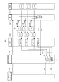
- FIG. 2 shows the configuration of the channel adapter 220.
- the channel adapter 220 includes a plurality of host channel control LSIs (large-scale integration) 510, a DMA LSI 520, and a plurality of intermediate buffers (DXBF) 530.
- the channel adapter 220 may have one host channel control LSI 510.
- the channel adapter 220 may have one intermediate buffer 530.
- the host channel control LSI 510 includes a communication control unit 511 and an internal buffer 512.
- the communication control unit 511 is connected to the host computer 400 and controls communication with the host computer 400 according to a predetermined protocol.
- the communication control unit 511 uses FICON (Fiber Connectivity) -HPF (High Performance), but other protocols may be used.
- the internal buffer 512 stores data to be transmitted to the host computer 400.
- the intermediate buffer 530 is a DRAM (Dynamic Random Access Memory), for example, and stores data transferred from the data cache 230 by the DMA LSI 520.
- DRAM Dynamic Random Access Memory
- the DMA LSI 520 includes a plurality of DMA controllers (DMAC) 521.
- DMAC DMA controllers
- Each of the plurality of DMA controllers 521 may be a different DMA circuit or a virtual DMA controller to which a DMA circuit is assigned.
- one DMA circuit in the DMA LSI 520 may be logically divided into a plurality of DMA controllers 521.
- the DMA circuit calculates a guarantee code.
- the guarantee code in this embodiment is a CRC, and the DMA circuit calculates a 4-byte CRC using an initial value of 4 bytes and an input having a length that is a multiple of 4 bytes.
- the CRC generator polynomial is represented by, for example, 0x04C11DB7.
- the guarantee code may be another error detection code or error correction code.
- the DMA controller 521 reads data from the data cache 230 in accordance with an instruction from the MP 240, performs CRC calculation based on the read data, and writes the read data to the intermediate buffer 530.
- FICON-HPF supports a multi-track read request for connecting and transferring a plurality of tracks by one read request.
- the track here is data of an arbitrary length specified in units of 1 byte.
- the storage apparatus 100 When the host computer 400 transmits a multitrack read request to the storage apparatus 100, the storage apparatus 100 performs multitrack read processing.
- the multi-track read request specifies a plurality of tracks.
- FIG. 3 shows an example of response data to the multitrack read request.
- the storage apparatus 100 Upon receipt of the multi-track read request, the storage apparatus 100 transmits to the host computer 400 response data in which a plurality of tracks are concatenated in the order requested, a final PAD, and a final CRC.
- Data obtained by concatenating the final PAD after the concatenated data is defined as the shaped data.
- the length of the shaped data is a multiple of 4 bytes.
- the final PAD is ALL zero data for adjusting the length.
- the final CRC is the CRC of the shaped data.
- the length of the final CRC is 4 bytes.
- the MP 240 calculates the smallest multiple of 4 bytes that is equal to or greater than the concatenated data length as the shaped data length, and calculates a value obtained by subtracting the concatenated data length from the shaped data length as the final PAD length. Further, when the final PAD length is not 0, the MP 240 generates a final PAD that is ALL zero data of the final PAD length.
- FIG. 4 schematically shows multitrack read processing.
- the multi-track read request here specifies three tracks T (0), T (1), and T (2) stored in the storage apparatus 100.
- the DMA LSI 520 includes three DMA controllers 521, X (0), X (1), and X (2).
- T (0), T (1), and T (2) indicate states stored in the data cache 230. If any of T (0), T (1), and T (2) is determined to be a cache miss, the disk adapter 250 reads the track determined to be a cache miss from the HDD 300 and writes it to the data cache 230.
- the host computer 400 issues a multitrack read request to the host channel control LSI 510 (S110).
- the host channel control LSI 510 sends the multitrack read request to the MP 240 (S120).
- the MP 240 Upon receiving the multitrack read request, the MP 240 assigns T (0) data transfer to X (0) and performs T (1) in order to perform data transfer of a plurality of tracks in parallel based on the multitrack read request. ) Is assigned to X (1), and T (2) is assigned to X (2). Thereafter, the MP 240 sends a transfer activation request designating T (0) to X (0) by CCW (channel command word) (S130), and sends a transfer activation request designating T (1) to X (1). Send (S140), a transfer activation request designating T (2) is sent to X (2) (S150).
- CCW channel command word
- X (0) activates DMA (0), which is T (0) DMA processing (S160).
- DMA (0) reads T (0) in the data cache 230, performs CRC calculation based on T (0), and transfers T (0) to the intermediate buffer 530.
- X (1) activates DMA (1), which is the DMA processing of T (1) (S170).
- DMA (1) reads T (1) in the data cache 230, performs CRC calculation based on T (1), and transfers T (1) to the intermediate buffer 530.
- X (2) activates DMA (2), which is the DMA processing of T (2) (S180). With DMA (2), X (2) reads T (2) in the data cache 230, performs CRC calculation based on T (2), and transfers T (2) to the intermediate buffer 530.
- X (0) When DMA (0) is completed, X (0) sends a transfer completion report indicating the result of DMA (0) to MP 240 (S190). When DMA (1) is completed, X (1) sends a transfer completion report indicating the result of DMA (1) to MP 240 (S200). When DMA (2) is completed, X (2) sends a transfer completion report indicating the result of DMA (2) to MP 240 (S210).
- the MP 240 Upon receiving the transfer completion report from X (0), X (1), and X (2), the MP 240 performs final CRC processing for calculating the final PAD and final CRC based on the transfer completion report (S220). Thereafter, the MP 240 writes the final PAD and the final CRC to the intermediate buffer 530 (S230), and sends a data transfer start instruction instructing transfer of response data to the host computer 400 to the host channel control LSI 510 (S240).
- the host channel control LSI 510 receives the data transfer start instruction, the host channel control LSI 510 reads T (0), T (1), T (2), final PAD, and final CRC from the intermediate buffer 530, and gives an address offset in units of 1 byte. , T (0), T (1), T (2), final PAD, and final CRC are concatenated and stored in the internal buffer 512 as response data (S250). Thereafter, the host channel control LSI 510 transmits response data to the host computer 400 (S260). When the transfer of the response data is completed, the host channel control LSI 510 transmits a status response to the multitrack read request to the host computer 400 (S270).
- the MP 240 assigns a plurality of tracks to be read to the plurality of DMA controllers 521, so that the plurality of DMA controllers 521 can perform a plurality of DMA processes in parallel.
- the MP 240 can perform calculation based on the processing results of the plurality of DMA controllers 521, thereby calculating the CRC of data in which a plurality of tracks are sequentially connected.
- any one of the intermediate buffer 530 and the internal buffer 512 may be used.
- the DMA controller 521 may transfer the data in the data cache 230 to the internal buffer 512.
- the communication control unit 511 may transfer the data in the intermediate buffer 530 to the host computer 400.
- FIG. 5 shows the DMA processing
- the transfer activation request includes a track length (transfer length), a transmission source address that is the address of the track in the data cache 230, a transmission destination address that is a transmission destination address in the intermediate buffer 530, and an initial CRC value. Including.
- the transfer activation request may include information indicating whether or not to generate the CRC of the track.
- the MP 240 designates 0xFFFFFF as the initial CRC value in the transfer activation request for the first track of the multi-track read request, and designates 0x00000000 as the initial CRC value in the transfer activation request for the track other than the first track.
- the initial CRC value in the transfer activation request to X (0) is 0xFFFFFF
- the initial CRC value in the transfer activation request to X (1) and X (2) is 0x00000000.
- the transfer activation request to each DMA controller 521 designates a predetermined value as the CRC initial value, it is not necessary to include the result of CRC calculation by another DMA controller 521.
- the DMA controller 521 obtains the track length from the transfer activation request, calculates a remainder obtained by dividing the track length by 4 bytes as a fraction data length, calculates a value obtained by subtracting the fraction data length from 4 bytes as a track PAD length, A value obtained by subtracting the fraction data length from the track length is calculated as a shortened data length, and a value obtained by adding the track PAD length to the track length is calculated as an extended data length.
- the DMA controller 521 extracts data from the beginning to the shortened data length of the track as shortened data, and extracts data of the fraction data length following the shortened data from the track as fraction data.
- the DMA controller 521 connects the track PAD, which is ALL zero data of the track PAD length, after the track to obtain extension data.
- the shortened data length is a multiple of the largest 4 bytes below the track length
- the extended data length is a multiple of the smallest 4 bytes above the track length.
- the DMA controller 521 reads the track from the transmission source address of the data cache 230, calculates the shortened data CRC which is the CRC of the shortened data, and writes the extended data to the destination address of the intermediate buffer 530.
- the DMA controller 521 sends a transfer completion report for the transfer activation request to the MP 240.
- the transfer completion report includes abbreviated data CRC and fraction data.
- X (0) divides T (0) into T (0) _t that is shortened data and T (0) _dat that is fractional data, and 0xFFFFFFFF T (0) _crc, which is the shortened data CRC, is calculated using the input T (0) _t as an initial value.
- X (1) divides T (1) into T (1) _t which is shortened data and T (1) _dat which is fractional data, and 0x00000000 is set as an initial value and T (1) _t is set as T (1) _t.
- T (1) _crc which is the shortened data CRC, is calculated as an input.
- T (2) _t which is shortened data
- T (2) _dat which is fractional data
- 0x00000000 is set as an initial value
- T (2) _t is set as T (2) _t.
- T (2) _crc which is the shortened data CRC, is calculated as an input.
- each DMA controller 521 uses the value specified by the MP 240 as the initial CRC value, so there is no need to take over the CRC calculated by another DMA controller 521. Thereby, the plurality of DMA controllers 521 can perform CRC calculation in parallel. Further, since the DMA controller 521 sends fractional data of less than 4 bytes to the MP 240 and does not perform CRC calculation of the fractional data, a DMA circuit that performs CRC calculation in units of 4 bytes can be used. Thereby, an increase in the circuit scale of the DMA controller 521 can be prevented.
- FIG. 6 shows the final CRC process.
- the track number is i
- the last track number is n
- the shortened data CRC of T (i) is T (i) _crc
- the fractional data of T (i) is T (i) _dat
- T The length (byte) of (i) is T (i) _len
- the temporary CRC is temp_crc
- the temporary data length is temp_len
- the length [byte] of the final PAD is pad_len.
- the MP 240 acquires T (i) _crc and T (i) _dat from the transfer completion report from the DMA controller 521.
- the MP 240 initializes variables (S310).
- the MP 240 substitutes 0 for i, and substitutes T (0) _crc for temp_crc.
- the MP 240 calculates a new temp_crc by performing CRC calculation with temp_crc as an initial value and T (i) _dat as an input (S320). If the CRC calculation function is Fd, this processing is expressed by the following equation.
- Temp_crc Fd (temp_crc, T (i) _dat)
- temp_crc becomes the CRC of the data up to T (i).
- the MP 240 calculates a new temp_crc by performing a CRC operation using temp_crc as an initial value and ALL zero data having a length of temp_len as an input (S360).
- a function for calculating CRC using a certain initial value and an input of ALL zero data having a certain length is Fz, this processing is expressed by the following equation.
- Temp_crc Fz (temp_crc, temp_len)
- the MP 240 calculates a new temp_crc by performing an XOR (exclusive OR) operation of temp_crc and T (i) _crc in bit units (S370), and shifts the processing to S320.
- XOR exclusive OR
- this processing is expressed by the following equation.
- Temp_crc becomes a CRC of data up to T (i) _t by the processing so far.
- the MP 240 sets the initial value as temp_crc, inputs ALL zero data of the length of pad_len, and performs a CRC operation to calculate a new temp_crc (S380). ).
- this process is expressed by the following equation.
- Temp_crc becomes the CRC of the shaped data by the processing so far.
- the MP 240 calculates the final CRC by performing bit inversion of temp_crc in accordance with the FICON-HPF specification (S390), and ends this flow. Using the aforementioned xor, this process is expressed by the following equation.
- Temp_crc temp_crc xor 0xFFFFFFFF
- the MP 240 can calculate the final CRC of the shaped data based on the shortened data CRC of each track calculated by the DMA controller 521.
- the MP 240 calculates the CRC of the fraction data, so that the track length can be specified in units of 1 byte, and the DMA controller 521 can perform CRC calculation in units of 4 bytes, and the circuit scale of the DMA controller 521 Can be prevented.
- the MP 240 sets the CRC of the data before the specific data among the concatenated data as an initial value, and sets the length of the specific data.
- the CRC of the data up to the specific data among the concatenated data can be calculated.
- the CRC of a plurality of data connected to the MP 240 can be calculated using the CRC calculation results of the plurality of data by the plurality of DMA controllers 521. Therefore, it is not necessary for another DMA controller 521 to take over the result of the CRC calculation by one DMA controller 521.
- the DMA controller 521 can perform CRC calculation in units of 4 bytes.
- the MP 240 may designate the initial CRC value in all DMA processes as 0x00000000, or may fix the initial CRC value in all DMA processes to 0x00000000. In this case, the MP 240 sets the initial CRC value in the final CRC process to 0xFFFFFF, inputs the zero data of the shortened data length of the first track, calculates the CRC, and performs the XOR operation between the CRC and the shortened data CRC. Thus, a result equal to the shortened data CRC calculated with the initial value of 0xFFFFFFFFFF can be obtained.
- the data length of T (0) is 67 bytes
- the data length of T (1) is 18 bytes
- the data length of T (2) is 33 bytes. Therefore, the concatenated data length is 118 bytes, the final PAD length is 2 bytes, and the shaped data length is 120 bytes that is a multiple of 4 bytes.
- X (0) divides 67 bytes of T (0) into 64 bytes of T (0) _t, which is a multiple of 4 bytes, and the remaining 3 bytes of T (0) _dat. Thereafter, X (0) calculates T (0) _crc by performing CRC calculation with 0xFFFFFF as an initial value and T (0) _t as an input.
- X (1) divides 18-byte T (1) into 16-byte T (1) _t, which is a multiple of 4 bytes, and the remaining 2-byte T (1) _dat. Thereafter, X (1) calculates T (1) _crc by performing CRC calculation with 0x00000000 as an initial value and T (1) _t as an input.
- X (2) divides 33-byte T (2) into 32-byte T (2) _t, which is a multiple of 4 bytes, and the remaining 1-byte T (2) _dat. Thereafter, X (2) calculates T (2) _crc by performing CRC calculation with 0x00000000 as an initial value and T (2) _t as an input.
- FIG. 7 shows a specific example of CRC final processing.
- the MP 240 calculates a new temp_crc by performing CRC calculation using T (0) _crc obtained from X (0) as an initial value and T (0) _dat obtained from X (0) as an input.
- This temp_crc is a CRC of data up to T (0).
- the MP 240 calculates a new temp_crc by performing a CRC operation using temp_crc as an initial value and 16-byte ALL zero data equal to the length of the shortened data of T (1) as an input. Thereafter, the MP 240 calculates a new temp_crc by performing an XOR operation between temp_crc and T (1) _crc obtained from X (1). After that, the MP 240 calculates a new temp_crc by performing CRC calculation using temp_crc as an initial value and T (1) _dat obtained from X (1) as an input. This temp_crc is a CRC of data up to T (1).
- the MP 240 calculates a new temp_crc by performing a CRC operation using temp_crc as an initial value and 32 bytes of ALL zero data equal to the length of the shortened data of T (2) as an input. After that, the MP 240 calculates a new temp_crc by performing an XOR operation between temp_crc and T (2) _crc obtained from X (2). After that, the MP 240 calculates a new temp_crc by performing CRC calculation using temp_crc as an initial value and T (2) _dat obtained from X (2) as an input. This temp_crc is a CRC of data up to T (2).
- the MP 240 calculates a new temp_crc by performing a CRC operation using the initial value as temp_crc and the 2-byte ALL zero data as the final PAD length as input.
- This temp_crc is a CRC of data up to the final PAD.
- the MP 240 calculates the final CRC by performing bit inversion of temp_crc.
- the shared memory stores a plurality of LUTs (Lookup Tables).
- the MP 240 calculates Fz by referring to the LUT according to the initial CRC value and the input ALL zero data length.
- the calculation method and the size and number of LUTs are determined by the performance required for the storage apparatus 100, the assumed ALL zero data length, the size of the shared memory, and the like.
- the initial value is 1 byte and the value is represented by Bi.
- Each of the plurality of LUTs stores CRCs for all Bi.
- the ALL zero data length of the prepared LUT is limited to a specific length.
- Lt is, for example, 1, 2, 3, 4, 16, 256, 4096. In order to speed up the calculation, more types of Lt may be prepared.
- Lt When Lt is less than 4, a LUT for each Lt is prepared.
- the CRC obtained from this LUT is represented by LUT [Lt] [Bi].
- Lt When Lt is 4 or more, the byte position of Bi in the initial value of 4 bytes is represented by Pb, and an LUT for each combination of Lt and Pb is prepared.
- the CRC obtained from this LUT is represented by LUT [Lt] [Pb] [Bi].
- MP240 calculates Fz by decomposing the ALL zero data length into combinations of Lt and performing CRC calculation corresponding to each decomposed Lt.
- LUT calculation processing which is CRC calculation of ALL zero data according to Lt will be described.
- each byte of temp_crc which is a 4-byte initial value, is represented by B0, B1, B2, and B3, and a left bit shift operator is represented by “ ⁇ ”.
- temp_crc LUT [1] [B0] XOR (B1 ⁇ 8) XOR (B2 ⁇ 16) XOR (B3 ⁇ 24)
- temp_crc LUT [2] [B0] XOR LUT [1] [B1] XOR (B2 ⁇ 16) XOR (B3 ⁇ 24)
- temp_crc LUT [3] [B0] XOR LUT [2] [B1] XOR LUT [1] [B2] XOR (B3 ⁇ 24)
- temp_crc LUT [Lt] [0] [B0] XOR LUT [Lt] [1] [B1] XOR LUT [Lt] [2] [B2] XOR LUT [Lt] [3] [B3]
- the MP 240 decomposes the ALL zero data length into L 4096 + 4096 + 256 + 4 + 4 + 2 and performs LUT operation processing corresponding to each Lt.
- the CRC calculation of the ALL zero data by the MP240 can be speeded up. Also, the number of LUTs can be reduced by decomposing the ALL zero data length into specific length combinations.
- the MP 240 may calculate the CRC of the fraction data using the LUT.
- the LUT has an initial value of 0x00000000 and stores a CRC calculation result for each input data of 1 byte.
- the MP 240 performs a bit shift on the CRC obtained from the LUT according to the length of the fraction data, and performs an XOR operation with the previous CRC.
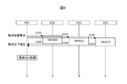
- FIG. 8 shows operations of the DMA controller 521 and the MP 240 regarding the CRC calculation.
- This sequence diagram shows the operation of the MP 240 and the DMA controller 521 X (0), X (1), and X (2).
- the MP 240 sends a transfer activation request to X (0), X (1), and X (2), respectively.
- X (0), X (1), and X (2) that have received the transfer activation request activate DMA (0), DMA (1), and DMA (2), respectively.
- X (0), X (1), and X (2) perform DMA processing in parallel.
- S190, S200, and S210 described above X (0), X (1), and X (2) that have completed the data transfer send a transfer completion report including the CRC calculation result to the MP240.
- the MP 240 calculates the final CRC by performing the final CRC processing using the CRC calculation results from X (0), X (1), and X (2) in order.
- a plurality of DMA controllers 521 can perform a CRC operation on a plurality of tracks in parallel, thereby transferring a plurality of tracks in parallel. Thereby, the performance of the multitrack read process can be improved.
- each track may be a multiple of 4 bytes.
- the MP 240 and the DMA controller 521 do not use fraction data, track PAD, final PAD, or the like.
- a channel controller connected to the host computer; A storage unit connected to the channel control unit; A processor connected to the channel control unit and the storage unit; With The channel control unit has a plurality of calculation units, When the processor receives a request to read a plurality of element data from the host computer, the processor specifies the plurality of element data for the plurality of arithmetic units, The plurality of arithmetic units respectively read the plurality of element data from the storage unit, calculate a plurality of partial codes that are a plurality of guarantee codes based on the plurality of element data, and send the plurality of parts to the processor.
- the processor calculates a sequence code that is a guarantee code of the sequence data including the plurality of concatenated element data based on the plurality of partial codes.
- Storage device (Expression 2) The plurality of calculation units calculate the plurality of partial codes in parallel, The storage device according to expression 1. (Expression 3) The guarantee code is a CRC having a predetermined length. The storage device according to expression 2. (Expression 4) Each of the plurality of arithmetic units extracts partial data that is data having a length that is a multiple of the predetermined length from the element data specified by the processor, and uses the predetermined code as an initial value of the partial code. The partial code is calculated by performing guarantee code calculation with data as input, The storage device according to expression 3.
- the processor temporarily performs a guarantee code calculation by using a guarantee code of data preceding the partial data in the series data as an initial value of the guarantee code, and inputting zero as a length equal to the partial data.
- a guarantee code is calculated, and a guarantee code of data up to the partial data in the series data is calculated by XOR operation of the temporary guarantee code and the partial code.
- the storage device according to expression 4. Each of the plurality of arithmetic units sends the fraction data to the processor when there is fraction data that is the remaining data of the partial data in the designated element data.
- the storage device according to expression 5.
- the processor performs a guarantee code calculation by using a guarantee code of data before the fraction data in the series data as an initial value of a guarantee code and the fraction data as an input, thereby performing the guarantee code calculation. Calculate the guarantee code for the data up to the fraction data,
- the storage device according to expression 6. The processor sends the predetermined code to each of the plurality of arithmetic units; The storage device according to expression 7.
- the predetermined code corresponding to the calculation unit in which element data other than the head of the plurality of element data is specified is zero of the predetermined length.
- the channel control unit further includes a buffer connected to the plurality of arithmetic units, and a communication control unit connected to the buffer, The plurality of arithmetic units respectively write the plurality of element data to the buffer, The processor writes the sequence code to the buffer; The communication control unit concatenates and transmits the sequence data and the sequence code in the buffer to the host computer.
- the storage device according to expression 9.
- a channel control unit connected to a host computer; a storage unit connected to the channel control unit; and a processor connected to the channel control unit and the storage unit, wherein the channel control unit includes a plurality of operations.
- a storage device control method for controlling a storage device having a storage unit When the processor receives a request to read a plurality of element data from the host computer, each of the plurality of element data is designated for the plurality of arithmetic units, The plurality of arithmetic units respectively read the plurality of element data from the storage unit, calculate a plurality of partial codes that are a plurality of guarantee codes based on the plurality of element data, and send the plurality of parts to the processor. Send each code, The processor calculates a sequence code that is a guarantee code of the sequence data including the plurality of element data connected based on the plurality of partial codes; A storage apparatus control method.
- the channel control unit corresponds to the channel adapter 220 and the like.
- the storage unit corresponds to the data cache 230, the HDD 300, or the like.
- the processor corresponds to the MP 240 and the like.
- the calculation unit corresponds to the DMA controller 521 and the like.
- the buffer corresponds to the intermediate buffer 530, the internal buffer 512, and the like.
- the communication control unit corresponds to the communication control unit 511 and the like.
- Element data corresponds to a track or the like.
- the partial data corresponds to shortened data or the like.
- the partial code corresponds to the shortened data CRC or the like.
- the series data corresponds to shaped data, concatenated data, and the like.
- the sequence code corresponds to the final CRC or the like.
- the predetermined code corresponds to 0xFFFFFFFF, 0x00000000, or the like.
- 100 storage device
- 200 storage controller
- 210 switch
- 220 channel adapter
- 230 data cache
- 250 disk adapter
- 400 host computer
- 510 host channel control LSI
- 511 communication control unit
- 512 internal Buffer
- 520 DMA LSI
- 521 DMA controller
- 530 intermediate buffer
Landscapes
- Engineering & Computer Science (AREA)
- Theoretical Computer Science (AREA)
- General Engineering & Computer Science (AREA)
- Physics & Mathematics (AREA)
- General Physics & Mathematics (AREA)
- Quality & Reliability (AREA)
- Computer Security & Cryptography (AREA)
- Bus Control (AREA)
Abstract
Description
LUT[1][B0] XOR (B1<<8)
XOR (B2<<16) XOR (B3<<24)
LUT[2][B0] XOR LUT[1][B1]
XOR (B2<<16) XOR (B3<<24)
LUT[3][B0] XOR LUT[2][B1]
XOR LUT[1][B2] XOR (B3<<24)
LUT[Lt][0][B0] XOR LUT[Lt][1][B1]
XOR LUT[Lt][2][B2] XOR LUT[Lt][3][B3]
(表現1)
ホストコンピュータに接続されるチャネル制御部と、
前記チャネル制御部に接続される記憶部と、
前記チャネル制御部及び前記記憶部に接続されるプロセッサと、
を備え、
前記チャネル制御部は、複数の演算部を有し、
前記プロセッサは、複数の要素データを読み出す要求を前記ホストコンピュータから受信した場合、前記複数の演算部に対して前記複数の要素データを夫々指定し、
前記複数の演算部は、前記記憶部から前記複数の要素データを夫々読み出し、前記複数の要素データに基づいて複数の保証コードである複数の部分コードを夫々算出し、前記プロセッサへ前記複数の部分コードを夫々送り、
前記プロセッサは、前記複数の部分コードに基づいて、連結された前記複数の要素データを含む系列データの保証コードである系列コードを算出する、
ストレージ装置。
(表現2)
前記複数の演算部は並列に、前記複数の部分コードを夫々算出する、
表現1に記載のストレージ装置。
(表現3)
前記保証コードは、所定長を有するCRCである、
表現2に記載のストレージ装置。
(表現4)
前記複数の演算部の夫々は、前記プロセッサにより指定された要素データから、前記所定長の倍数の長さを有するデータである部分データを抽出し、所定コードを部分コードの初期値として、前記部分データを入力として、保証コード演算を行うことにより前記部分コードを算出する、
表現3に記載のストレージ装置。
(表現5)
前記プロセッサは、前記系列データの内の前記部分データより前のデータの保証コードを保証コードの初期値として、前記部分データに等しい長さのゼロを入力として、保証コード演算を行うことにより、一時的な保証コードを算出し、前記一時的な保証コードと前記部分コードのXOR演算により、前記系列データの内の前記部分データまでのデータの保証コードを算出する、
表現4に記載のストレージ装置。
(表現6)
前記複数の演算部の夫々は、前記指定された要素データ内に前記部分データの残りのデータである端数データがある場合、前記端数データを前記プロセッサへ送る、
表現5に記載のストレージ装置。
(表現7)
前記プロセッサは、前記系列データの内の前記端数データより前のデータの保証コードを保証コードの初期値として、前記端数データを入力として、保証コード演算を行うことにより、前記系列データの内の前記端数データまでのデータの保証コードを算出する、
表現6に記載のストレージ装置。
(表現8)
前記プロセッサは、前記所定コードを前記複数の演算部の夫々へ送る、
表現7に記載のストレージ装置。
(表現9)
前記複数の要素データの中の先頭以外の要素データが指定された演算部に対応する所定コードは、前記所定長のゼロである、
表現8に記載のストレージ装置。
(表現10)
前記チャネル制御部は更に、前記複数の演算部に接続されたバッファと、前記バッファに接続された通信制御部とを有し、
前記複数の演算部は、前記複数の要素データを前記バッファへ夫々書き込み、
前記プロセッサは、前記系列コードを前記バッファへ書き込み、
前記通信制御部は、前記バッファ内の前記系列データ及び前記系列コードを連結して前記ホストコンピュータへ送信する、
表現9に記載のストレージ装置。
(表現11)
ホストコンピュータに接続されるチャネル制御部と、前記チャネル制御部に接続される記憶部と、前記チャネル制御部及び前記記憶部に接続されるプロセッサとを有し、前記チャネル制御部が、複数の演算部を有するストレージ装置を、制御するためのストレージ装置制御方法であって、
前記プロセッサが、複数の要素データを読み出す要求を前記ホストコンピュータから受信した場合、前記複数の演算部に対して前記複数の要素データを夫々指定し、
前記複数の演算部が、前記記憶部から前記複数の要素データを夫々読み出し、前記複数の要素データに基づいて複数の保証コードである複数の部分コードを夫々算出し、前記プロセッサへ前記複数の部分コードを夫々送り、
前記プロセッサが、前記複数の部分コードに基づいて、連結された前記複数の要素データを含む系列データの保証コードである系列コードを算出する、
ことを備えるストレージ装置制御方法。
Claims (11)
- ホストコンピュータに接続されるチャネル制御部と、
前記チャネル制御部に接続される記憶部と、
前記チャネル制御部及び前記記憶部に接続されるプロセッサと、
を備え、
前記チャネル制御部は、複数の演算部を有し、
前記プロセッサは、複数の要素データを読み出す要求を前記ホストコンピュータから受信した場合、前記複数の演算部に対して前記複数の要素データを夫々指定し、
前記複数の演算部は、前記記憶部から前記複数の要素データを夫々読み出し、前記複数の要素データに基づいて複数の保証コードである複数の部分コードを夫々算出し、前記プロセッサへ前記複数の部分コードを夫々送り、
前記プロセッサは、前記複数の部分コードに基づいて、連結された前記複数の要素データを含む系列データの保証コードである系列コードを算出する、
ストレージ装置。 - 前記複数の演算部は並列に、前記複数の部分コードを夫々算出する、
請求項1に記載のストレージ装置。 - 前記保証コードは、所定長を有するCRCである、
請求項2に記載のストレージ装置。 - 前記複数の演算部の夫々は、前記プロセッサにより指定された要素データから、前記所定長の倍数の長さを有するデータである部分データを抽出し、所定コードを部分コードの初期値として、前記部分データを入力として、保証コード演算を行うことにより前記部分コードを算出する、
請求項3に記載のストレージ装置。 - 前記プロセッサは、前記系列データの内の前記部分データより前のデータの保証コードを保証コードの初期値として、前記部分データに等しい長さのゼロを入力として、保証コード演算を行うことにより、一時的な保証コードを算出し、前記一時的な保証コードと前記部分コードのXOR演算により、前記系列データの内の前記部分データまでのデータの保証コードを算出する、
請求項4に記載のストレージ装置。 - 前記複数の演算部の夫々は、前記指定された要素データ内に前記部分データの残りのデータである端数データがある場合、前記端数データを前記プロセッサへ送る、
請求項5に記載のストレージ装置。 - 前記プロセッサは、前記系列データの内の前記端数データより前のデータの保証コードを保証コードの初期値として、前記端数データを入力として、保証コード演算を行うことにより、前記系列データの内の前記端数データまでのデータの保証コードを算出する、
請求項6に記載のストレージ装置。 - 前記プロセッサは、前記所定コードを前記複数の演算部の夫々へ送る、
請求項7に記載のストレージ装置。 - 前記複数の要素データの中の先頭以外の要素データが指定された演算部に対応する所定コードは、前記所定長のゼロである、
請求項8に記載のストレージ装置。 - 前記チャネル制御部は更に、前記複数の演算部に接続されたバッファと、前記バッファに接続された通信制御部とを有し、
前記複数の演算部は、前記複数の要素データを前記バッファへ夫々書き込み、
前記プロセッサは、前記系列コードを前記バッファへ書き込み、
前記通信制御部は、前記バッファ内の前記系列データ及び前記系列コードを連結して前記ホストコンピュータへ送信する、
請求項9に記載のストレージ装置。 - ホストコンピュータに接続されるチャネル制御部と、前記チャネル制御部に接続される記憶部と、前記チャネル制御部及び前記記憶部に接続されるプロセッサとを有し、前記チャネル制御部が、複数の演算部を有するストレージ装置を、制御するためのストレージ装置制御方法であって、
前記プロセッサが、複数の要素データを読み出す要求を前記ホストコンピュータから受信した場合、前記複数の演算部に対して前記複数の要素データを夫々指定し、
前記複数の演算部が、前記記憶部から前記複数の要素データを夫々読み出し、前記複数の要素データに基づいて複数の保証コードである複数の部分コードを夫々算出し、前記プロセッサへ前記複数の部分コードを夫々送り、
前記プロセッサが、前記複数の部分コードに基づいて、連結された前記複数の要素データを含む系列データの保証コードである系列コードを算出する、
ことを備えるストレージ装置制御方法。
Priority Applications (3)
| Application Number | Priority Date | Filing Date | Title |
|---|---|---|---|
| JP2014558362A JP6046750B2 (ja) | 2013-01-24 | 2013-01-24 | ストレージ装置およびストレージ装置制御方法 |
| PCT/JP2013/051392 WO2014115277A1 (ja) | 2013-01-24 | 2013-01-24 | ストレージ装置およびストレージ装置制御方法 |
| US14/758,929 US9720767B2 (en) | 2013-01-24 | 2013-01-24 | Storage apparatus and storage apparatus control method |
Applications Claiming Priority (1)
| Application Number | Priority Date | Filing Date | Title |
|---|---|---|---|
| PCT/JP2013/051392 WO2014115277A1 (ja) | 2013-01-24 | 2013-01-24 | ストレージ装置およびストレージ装置制御方法 |
Publications (1)
| Publication Number | Publication Date |
|---|---|
| WO2014115277A1 true WO2014115277A1 (ja) | 2014-07-31 |
Family
ID=51227093
Family Applications (1)
| Application Number | Title | Priority Date | Filing Date |
|---|---|---|---|
| PCT/JP2013/051392 Ceased WO2014115277A1 (ja) | 2013-01-24 | 2013-01-24 | ストレージ装置およびストレージ装置制御方法 |
Country Status (3)
| Country | Link |
|---|---|
| US (1) | US9720767B2 (ja) |
| JP (1) | JP6046750B2 (ja) |
| WO (1) | WO2014115277A1 (ja) |
Cited By (1)
| Publication number | Priority date | Publication date | Assignee | Title |
|---|---|---|---|---|
| US11474751B2 (en) | 2021-02-25 | 2022-10-18 | Hitachi, Ltd. | Storage apparatus and data processing method therefor |
Families Citing this family (3)
| Publication number | Priority date | Publication date | Assignee | Title |
|---|---|---|---|---|
| US10503582B2 (en) | 2017-03-06 | 2019-12-10 | Tttech Auto Ag | Method and computer system for fault tolerant data integrity verification of safety-related data |
| US10901654B2 (en) * | 2018-10-30 | 2021-01-26 | International Business Machines Corporation | Buffer credit management in a data storage system |
| US12088411B2 (en) * | 2022-08-25 | 2024-09-10 | Semiconductor Components Industries, Llc | Cyclic redundancy check (CRC) generation |
Citations (5)
| Publication number | Priority date | Publication date | Assignee | Title |
|---|---|---|---|---|
| JPH09116541A (ja) * | 1995-10-16 | 1997-05-02 | Toshiba Corp | 通信制御装置 |
| JP2002185438A (ja) * | 2000-12-11 | 2002-06-28 | Matsushita Electric Ind Co Ltd | Crc演算装置 |
| JP2004173178A (ja) * | 2002-11-22 | 2004-06-17 | Nec Corp | 伝送システムおよび伝送装置 |
| WO2010095173A1 (en) * | 2009-02-19 | 2010-08-26 | Hitachi, Ltd. | Storage apparatus and data integrity assurance method |
| JP2011176597A (ja) * | 2010-02-24 | 2011-09-08 | Panasonic Corp | 符号化装置及び符号化方法 |
Family Cites Families (5)
| Publication number | Priority date | Publication date | Assignee | Title |
|---|---|---|---|---|
| JP4260688B2 (ja) * | 2004-06-09 | 2009-04-30 | 富士通株式会社 | データ送信装置、データ送受信システム、データ送信装置の制御方法およびデータ送受信システムの制御方法 |
| JP2008117253A (ja) | 2006-11-07 | 2008-05-22 | Hitachi Ltd | 記憶装置システムと計算機システムおよびその処理方法 |
| JP4747077B2 (ja) * | 2006-11-16 | 2011-08-10 | ルネサスエレクトロニクス株式会社 | 演算回路 |
| JP4906562B2 (ja) | 2007-04-02 | 2012-03-28 | 株式会社日立製作所 | ストレージ装置及びボリューム復元方法 |
| JP4831018B2 (ja) * | 2007-08-28 | 2011-12-07 | 日本電気株式会社 | 並列巡回符号生成装置および並列巡回符号検査装置 |
-
2013
- 2013-01-24 JP JP2014558362A patent/JP6046750B2/ja active Active
- 2013-01-24 WO PCT/JP2013/051392 patent/WO2014115277A1/ja not_active Ceased
- 2013-01-24 US US14/758,929 patent/US9720767B2/en active Active
Patent Citations (5)
| Publication number | Priority date | Publication date | Assignee | Title |
|---|---|---|---|---|
| JPH09116541A (ja) * | 1995-10-16 | 1997-05-02 | Toshiba Corp | 通信制御装置 |
| JP2002185438A (ja) * | 2000-12-11 | 2002-06-28 | Matsushita Electric Ind Co Ltd | Crc演算装置 |
| JP2004173178A (ja) * | 2002-11-22 | 2004-06-17 | Nec Corp | 伝送システムおよび伝送装置 |
| WO2010095173A1 (en) * | 2009-02-19 | 2010-08-26 | Hitachi, Ltd. | Storage apparatus and data integrity assurance method |
| JP2011176597A (ja) * | 2010-02-24 | 2011-09-08 | Panasonic Corp | 符号化装置及び符号化方法 |
Cited By (1)
| Publication number | Priority date | Publication date | Assignee | Title |
|---|---|---|---|---|
| US11474751B2 (en) | 2021-02-25 | 2022-10-18 | Hitachi, Ltd. | Storage apparatus and data processing method therefor |
Also Published As
| Publication number | Publication date |
|---|---|
| JPWO2014115277A1 (ja) | 2017-01-19 |
| US20150339184A1 (en) | 2015-11-26 |
| US9720767B2 (en) | 2017-08-01 |
| JP6046750B2 (ja) | 2016-12-21 |
Similar Documents
| Publication | Publication Date | Title |
|---|---|---|
| CN111435292B (zh) | 利用自适应写缓冲区释放的存储介质编程 | |
| JP5437922B2 (ja) | 同時データ操作が可能なdmaエンジン | |
| JP5159902B2 (ja) | 入出力処理システム内のチャネル・サブシステムと通信するように構成された制御装置において可変長のデバイス・コマンド・ワード(dcw)を処理するための方法 | |
| US8762609B1 (en) | System and method for multiengine operation with super descriptor in SAS/SATA controller wherein portion of super-descriptor is executed without intervention of initiator | |
| JP5107880B2 (ja) | データ転送処理装置及び方法 | |
| TWI466126B (zh) | 多通道儲存裝置及在其中儲存資料之方法 | |
| EP4264407B1 (en) | Method and apparatus for controlling a computational storage processor | |
| US8924606B2 (en) | Storage system and data transfer control method | |
| CN111625181B (zh) | 数据处理方法、独立硬盘冗余阵列控制器和数据存储系统 | |
| TW201901426A (zh) | 非揮發性記憶體裝置及其讀取方法 | |
| CN114328316A (zh) | Dma控制器、soc系统及基于dma控制器的数据搬运方法 | |
| JP2011512591A5 (ja) | ||
| CN101206612B (zh) | 信息处理装置以及历史管理方法 | |
| JP6649989B2 (ja) | ストレージシステム及びその制御方法 | |
| JP6046750B2 (ja) | ストレージ装置およびストレージ装置制御方法 | |
| JP6426838B2 (ja) | ストレージシステム、及び、記憶制御方法 | |
| US9213486B2 (en) | Writing new data of a first block size to a second block size using a write-write mode | |
| TWI865071B (zh) | 用於使用卸載主機任務的非揮發性儲存裝置進行資料處理的方法、系統及非暫態性處理器可讀取媒體 | |
| JP4394533B2 (ja) | ディスクアレイシステム | |
| CN120523392A (zh) | 用于管理读和写操作的数据完整性的系统和方法 | |
| CN101241478B (zh) | 数据传送方法 | |
| CN109445686A (zh) | 一种存储磁盘以及存取数据的方法 | |
| JP2019095844A (ja) | データ転送装置およびデータ転送方法 | |
| US20250110819A1 (en) | Memory Access Validation for Input/Output Operations Using an Interposer | |
| JP2007079715A (ja) | データ転送方法、プログラムおよび装置 |
Legal Events
| Date | Code | Title | Description |
|---|---|---|---|
| 121 | Ep: the epo has been informed by wipo that ep was designated in this application |
Ref document number: 13872592 Country of ref document: EP Kind code of ref document: A1 |
|
| ENP | Entry into the national phase |
Ref document number: 2014558362 Country of ref document: JP Kind code of ref document: A |
|
| WWE | Wipo information: entry into national phase |
Ref document number: 14758929 Country of ref document: US |
|
| NENP | Non-entry into the national phase |
Ref country code: DE |
|
| 122 | Ep: pct application non-entry in european phase |
Ref document number: 13872592 Country of ref document: EP Kind code of ref document: A1 |