WO2014112150A1 - 受電装置、送電装置および電力伝送システム - Google Patents
受電装置、送電装置および電力伝送システム Download PDFInfo
- Publication number
- WO2014112150A1 WO2014112150A1 PCT/JP2013/073317 JP2013073317W WO2014112150A1 WO 2014112150 A1 WO2014112150 A1 WO 2014112150A1 JP 2013073317 W JP2013073317 W JP 2013073317W WO 2014112150 A1 WO2014112150 A1 WO 2014112150A1
- Authority
- WO
- WIPO (PCT)
- Prior art keywords
- power
- electrode
- power transmission
- wireless communication
- conductor
- Prior art date
- Legal status (The legal status is an assumption and is not a legal conclusion. Google has not performed a legal analysis and makes no representation as to the accuracy of the status listed.)
- Ceased
Links
Images









Classifications
-
- H—ELECTRICITY
- H04—ELECTRIC COMMUNICATION TECHNIQUE
- H04B—TRANSMISSION
- H04B5/00—Near-field transmission systems, e.g. inductive or capacitive transmission systems
- H04B5/70—Near-field transmission systems, e.g. inductive or capacitive transmission systems specially adapted for specific purposes
- H04B5/79—Near-field transmission systems, e.g. inductive or capacitive transmission systems specially adapted for specific purposes for data transfer in combination with power transfer
-
- H—ELECTRICITY
- H02—GENERATION; CONVERSION OR DISTRIBUTION OF ELECTRIC POWER
- H02J—ELECTRIC POWER NETWORKS; CIRCUIT ARRANGEMENTS OR SYSTEMS FOR SUPPLYING OR DISTRIBUTING ELECTRIC POWER; SYSTEMS FOR STORING ELECTRIC ENERGY
- H02J50/00—Circuit arrangements or systems for wireless supply or distribution of electric power
-
- H—ELECTRICITY
- H01—ELECTRIC ELEMENTS
- H01Q—ANTENNAS, i.e. RADIO AERIALS
- H01Q7/00—Loop antennas with a substantially uniform current distribution around the loop and having a directional radiation pattern in a plane perpendicular to the plane of the loop
-
- H—ELECTRICITY
- H02—GENERATION; CONVERSION OR DISTRIBUTION OF ELECTRIC POWER
- H02J—ELECTRIC POWER NETWORKS; CIRCUIT ARRANGEMENTS OR SYSTEMS FOR SUPPLYING OR DISTRIBUTING ELECTRIC POWER; SYSTEMS FOR STORING ELECTRIC ENERGY
- H02J50/00—Circuit arrangements or systems for wireless supply or distribution of electric power
- H02J50/05—Circuit arrangements or systems for wireless supply or distribution of electric power using capacitive coupling
-
- H—ELECTRICITY
- H02—GENERATION; CONVERSION OR DISTRIBUTION OF ELECTRIC POWER
- H02J—ELECTRIC POWER NETWORKS; CIRCUIT ARRANGEMENTS OR SYSTEMS FOR SUPPLYING OR DISTRIBUTING ELECTRIC POWER; SYSTEMS FOR STORING ELECTRIC ENERGY
- H02J50/00—Circuit arrangements or systems for wireless supply or distribution of electric power
- H02J50/20—Circuit arrangements or systems for wireless supply or distribution of electric power using microwaves or radio frequency waves
-
- H—ELECTRICITY
- H02—GENERATION; CONVERSION OR DISTRIBUTION OF ELECTRIC POWER
- H02J—ELECTRIC POWER NETWORKS; CIRCUIT ARRANGEMENTS OR SYSTEMS FOR SUPPLYING OR DISTRIBUTING ELECTRIC POWER; SYSTEMS FOR STORING ELECTRIC ENERGY
- H02J50/00—Circuit arrangements or systems for wireless supply or distribution of electric power
- H02J50/80—Circuit arrangements or systems for wireless supply or distribution of electric power involving the exchange of data, concerning supply or distribution of electric power, between transmitting devices and receiving devices
-
- H—ELECTRICITY
- H04—ELECTRIC COMMUNICATION TECHNIQUE
- H04B—TRANSMISSION
- H04B5/00—Near-field transmission systems, e.g. inductive or capacitive transmission systems
- H04B5/20—Near-field transmission systems, e.g. inductive or capacitive transmission systems characterised by the transmission technique; characterised by the transmission medium
- H04B5/24—Inductive coupling
-
- H—ELECTRICITY
- H02—GENERATION; CONVERSION OR DISTRIBUTION OF ELECTRIC POWER
- H02J—ELECTRIC POWER NETWORKS; CIRCUIT ARRANGEMENTS OR SYSTEMS FOR SUPPLYING OR DISTRIBUTING ELECTRIC POWER; SYSTEMS FOR STORING ELECTRIC ENERGY
- H02J50/00—Circuit arrangements or systems for wireless supply or distribution of electric power
- H02J50/005—Mechanical details of housing or structure aiming to accommodate the power transfer means, e.g. mechanical integration of coils, antennas or transducers into emitting or receiving devices
Definitions
- the present invention relates to a power reception device, a power transmission device, and a power transmission system, and particularly to a power reception device, a power transmission device, and a power transmission system corresponding to the electric field coupling method.
- Patent Document 1 An example of an apparatus that transmits electric power by an electric field coupling method is disclosed in Patent Document 1.
- This device is composed of an energy generating device and a consuming device located at a short distance from each other.
- the device is also modeled in the form of an interaction between asymmetric oscillating electric dipoles, which consists of a high-voltage high-frequency generator or a high-voltage high-frequency charge placed between two electrodes. These dipoles exert mutual influence on each other. Electrical energy and / or information is transported remotely using a Coulomb field surrounding any collection of charged conductors in a slowly changing variable state.
- Patent Document 2 discloses an example of an electronic device that performs wireless communication by a magnetic field coupling method.
- This electronic device includes a loop-shaped or spiral coil conductor having a winding center portion as a coil opening, and a conductor layer having a conductor opening and a slit portion leading to the conductor opening.
- the coil conductor When the coil conductor is viewed in plan, the coil opening overlaps with the conductor opening, the area of the conductor layer is larger than the area of the coil conductor formation region, and the magnetic sheet is provided so as to cover the coil opening and the conductor opening. .
- stable communication is possible even if the antenna is smaller than the communication partner antenna.
- Patent Document 1 and the wireless communication of Patent Document 2 are to be realized by a single device, it is necessary to mount both the transmitting / receiving antenna and the power transmitting / receiving electrode on the device.
- the size of the device is limited, desired performance cannot be secured for at least one of power transmission and wireless communication.
- the transmission / reception antenna and the power transmission / reception electrode are arranged close to each other, one interferes with the other, thereby degrading the power transmission performance or the wireless communication performance.
- a main object of the present invention is to provide a power receiving device, a power transmitting device, and a power transmission system capable of improving both power transmission performance and wireless communication performance.
- a power receiving device (30: reference numeral corresponding to the embodiment; the same applies hereinafter) includes a power supply coil (40) for wireless communication, a wireless IC chip (43), and a power supply circuit (42).
- Short-range wireless communication means (42-43) for transmitting and receiving high-frequency signals via the first electrode (E21) for electric field coupling with the power transmission device (10), and a booster antenna magnetically coupled with the feeding coil during wireless communication with the power transmission device Conductor (E22, E22_1, E22_2) that functions as a second electrode that functions as a second electrode that cooperates with the first electrode when receiving power from the power transmission device and is coupled with the power transmission device, and the first electrode and the conductor by electric field coupling Supply means (34 to 38) for supplying power based on the alternating voltage excited to the load (46).
- the supply means includes step-down means (34) for stepping down the AC voltage excited by the first electrode and the conductor, and rectification means (36) for rectifying the AC voltage stepped down by the step-down means.
- blocking means SW21 to SW22, S5 to S11 for blocking the connection between at least one of the first electrode and the conductor and the supply means during wireless communication.
- the area of the first electrode is smaller than the area of the second electrode.
- a power receiving surface facing the power transmission device is further provided, and the conductor is provided at the same distance as the first electrode or a distance farther than the first electrode with respect to the power receiving surface, and the power feeding coil is farther from the conductor. Provided at distance.
- the conductor is disposed so as to surround the first electrode.
- the power feeding coil is a planar coil, and the coil opening is disposed so as to face the power receiving surface, and a magnetic body (MG) provided on a surface far from the power receiving surface of the power feeding coil is further provided.
- MG magnetic body
- a power transmission device (10) includes a power supply coil (26) for wireless communication, a wireless IC chip (23), and a power supply circuit (24), and transmits and receives a high-frequency signal via the power supply coil. It functions as a booster antenna that magnetically couples to the power supply coil during wireless communication with the communication means (23 to 24), the power receiving device (30), and the first electrode (E11) that is electrically coupled to the power receiving device.
- a conductor (E12_1, E12_2) functioning as a second electrode that is electrically coupled to the power receiving device in cooperation with one electrode, and an AC voltage output from the AC voltage source (18) is supplied to the first electrode and the conductor.
- Supply means (20) is provided.
- a power transmission system (100) includes a power transmission device (10) that transmits an AC voltage by an electric field coupling method, and a power reception device (30) that receives an AC voltage transmitted from the power transmission device by an electric field coupling method.
- the power receiving device includes a power supply coil (40) for wireless communication, a wireless IC chip (43), and a power supply circuit (42), and transmits and receives high-frequency signals through the power supply coil.
- Conductor (E22, E22_1, E22_2) functioning as a second electrode that is electric field coupled to the power transmission device in cooperation with one electrode, and load based on AC voltage excited to the first electrode and the conductor by electric field coupling Supply means (34-38) to supply (46) 1952.
- a power transmission system (100) includes a power transmission device (10) that transmits an AC voltage by an electric field coupling method, and a power reception device (30) that receives an AC voltage transmitted from the power transmission device by an electric field coupling method.
- a transmission system, a power transmission device includes a power supply coil (26) for wireless communication, a wireless IC chip (23), and a power supply circuit (24), and transmits and receives high-frequency signals via the power supply coil. It functions as a booster antenna that magnetically couples to the power supply coil during wireless communication with the communication means (23 to 24), the power receiving device (30), and the first electrode (E11) that is electrically coupled to the power receiving device.
- Supply means (20) is provided.
- the conductor when receiving power, the conductor functions as the second electrode for electric field coupling.
- the electric field coupling with the power transmission device is realized by the first electrode and the conductor, and the electric power based on the AC voltage excited by the first electrode and the conductor is supplied to the load by the supply means.
- the conductor functions as a booster antenna.
- the high-frequency signal received from the power transmission device is input to the short-range wireless communication means via the booster antenna and the power supply coil, and the high-frequency signal output from the short-range wireless communication means is transmitted to the power transmission device via the power supply coil and the booster antenna. Is done.
- the conductor can be shared as an electrode for electric field coupling and an antenna for wireless communication, and both the power transmission performance and the wireless communication performance can be improved even if it is small.
- the conductor functions as the second electrode for electric field coupling.
- the electric field coupling with the power receiving device is realized by the first electrode and the conductor, and the AC voltage output from the AC voltage source is supplied to the first electrode and the conductor by the supply means.
- the conductor functions as a booster antenna.
- the high-frequency signal output from the short-range wireless communication means is transmitted to the power receiving device via the power feeding coil and the booster antenna, and the high-frequency signal received from the power receiving device is input to the short-range wireless communication means via the booster antenna and the power feeding coil. Is done.
- the conductor can be shared as an electrode for electric field coupling and an antenna for wireless communication, and both the power transmission performance and the wireless communication performance can be improved even if it is small.
- FIG. 4 is a cross-sectional view of the power receiving device shown in FIG. 3 taken along the line AA.
- A) is an illustrative view showing an example of a laminated structure of an active electrode, a passive electrode, an antenna coil, and a magnetic sheet provided in the power receiving device shown in FIG. 3, and
- B) is an illustration of the laminated structure shown in (A). It is BB sectional drawing.
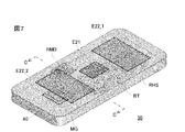
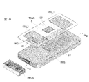
- FIG. 8 is a CC cross-sectional view of the power receiving device shown in FIG. 7. It is an illustration figure which shows the positional relationship of the active electrode, the passive electrode, and antenna coil which were provided in the power receiving apparatus shown in FIG. It is a disassembled perspective view which shows an example of the external appearance of the power receiving apparatus applied to the power transmission system of another Example.
- FIG. 11 is a DD cross-sectional view of the power receiving device shown in FIG. 10.
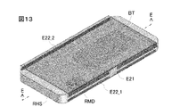
- FIG. 14A is a cross-sectional view taken along line EE of the power receiving device shown in FIG. 13, and FIG. 14B is a long side view of the power receiving device shown in FIG.
- FIG. 14A is a cross-sectional view taken along line EE of the power receiving device shown in FIG. 13, and FIG. 14B is a long side view of the power receiving device shown in FIG.
- FIG. 14A is a cross-sectional view taken along line EE of the power receiving device shown in FIG. 13, and FIG. 14B is a long side view of the power receiving device shown in FIG.
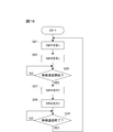
- It is a block diagram which shows the structure of the electric power transmission system of another Example. It is a flowchart which shows a part of operation
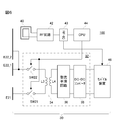
- a power transmission system 100 includes a power transmission device 10 that transmits a high-frequency voltage of 100 kHz to 10 MHz by an electric field coupling method, and receives a high-frequency voltage transmitted from the power transmission device 10 by an electric field coupling method.
- Power receiving device 30 The power transmission device 10 and the power reception device 30 have a wireless communication function for communicating a high frequency signal of 13.56 MHz.
- a high-frequency voltage to be transmitted is generated by the power transmission circuit 14, and a high-frequency signal is input / output by the RF-IC 23 and the RF circuit (power feeding circuit) 24 under the control of the CPU 22.
- the RF-IC 23 is driven by a DC power supply 12b.
- the received high frequency voltage is converted into a DC voltage by the power receiving circuit 32, and the high frequency signal is input / output by the RF-IC 43 and the RF circuit (power feeding circuit) 42 under the control of the CPU 44.
- the control circuit 16 provided in the power transmission circuit 14 gives a PWM signal having a frequency of 100 kHz to 10 MHz to the drive circuit 18.
- the drive circuit 18 converts the DC voltage supplied from the DC power supply 12a into a high frequency voltage in accordance with the PWM signal supplied from the control circuit 16.
- the frequency of the converted high-frequency voltage matches the frequency of the PWM signal, and the level of the converted high-frequency voltage depends on the duty ratio of the PWM signal.
- the converted high-frequency voltage is applied to the primary winding L1 that forms the step-up transformer 20.
- the secondary winding L2 forming the step-up transformer 20 is excited with a high-frequency voltage boosted to a different voltage depending on the transformation ratio.
- One end and the other end of the secondary winding L2 are connected to an active electrode (small electrode) E11 and a passive electrode (large electrode) E12 for electric field coupling. Therefore, the high-frequency voltage boosted by the step-up transformer 20 is applied to the active electrode E11 and the passive electrode E12.
- the power receiving device 30 is provided with an active electrode E21 and a passive electrode E22 for electric field coupling.
- the active electrode E21 is connected to one end of the primary winding L3 via a switch SW21 provided in the power receiving circuit 32
- the passive electrode E22 is connected to the other end of the primary winding L3 via a switch SW22 provided in the power receiving circuit 32. Connected.
- the primary winding L3 and the secondary winding L4 form a step-down transformer 34.
- the switches SW21 and SW22 are turned on by the CPU 44 at a time other than during wireless communication. Therefore, when a high-frequency voltage is excited in the active electrode E21 and the passive electrode E22 by electric field coupling with the active electrode E21 and the passive electrode E22 provided in the power transmission device 10, a high-frequency signal indicating a level corresponding to the step-down ratio of the step-down transformer 34. The voltage is also excited in the secondary coil L4.
- the rectifying / smoothing circuit 36 rectifies and smoothes the high-frequency voltage excited by the secondary coil L4.
- the DC-DC converter 38 adjusts the level of the DC voltage generated thereby, and supplies the DC voltage having the adjusted level to the mobile device 46.
- the RF-IC 23 provided in the power transmission apparatus 10 provides a baseband signal to the RF circuit 24 when performing wireless communication with the power reception apparatus 30.
- the RF circuit 24 modulates a given baseband signal into a high-frequency signal, and transmits the modulated high-frequency signal through a large antenna coil (feeding coil) 26.
- the CPU 44 provided in the power receiving device 30 turns off the switches SW21 and SW22 when performing wireless communication with the power transmitting device 10. Accordingly, the passive electrode E22 functions as a booster antenna that is magnetically coupled to the small antenna coil (feeding coil) 40.
- the high-frequency signal transmitted from the power transmission device 10 is input to the RF circuit 42 via the passive electrode E22 and the antenna coil 40.
- the RF circuit 42 demodulates the input high-frequency signal into a baseband signal, and gives the demodulated baseband signal to the RF-IC 43.
- the baseband signal output from the RF-IC 43 is modulated into a high frequency signal by the RF circuit 42, and the modulated high frequency signal is transmitted via the antenna coil 40 and the passive electrode E22.
- the transmitted high frequency signal is input to the RF circuit 24 via the antenna coil 26 of the power transmission circuit 10 and demodulated into a baseband signal.
- the demodulated burst band signal is supplied to the RF-IC 23.
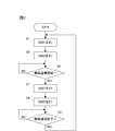
- step S1 In connection with the on / off control of the switches SW21 and SW22, the CPU 44 executes processing according to the flowchart shown in FIG. First, the switch SW21 is turned on in step S1, and the switch SW22 is turned on in step S3. In step S5, it is repeatedly determined whether or not wireless communication is started. When the determination result is updated from NO to YES, the switch SW21 is turned off in step S7, and the switch SW22 is turned off in step S9. In step S11, it is repeatedly determined whether or not the wireless communication is terminated, and when the determination result is updated from NO to YES, the process returns to step S1.
- step S1 and step S3 may be reversed or may be performed simultaneously.
- Steps S7 and S9 may also be reversed or performed simultaneously.
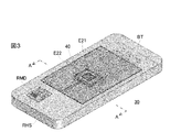
- power reception device 30 has a plate-shaped or rectangular parallelepiped housing RHS in which each of one main surface and the other main surface is a rectangle.
- the housing RHS houses the battery BT, and further houses the power receiving module RMD on which the power receiving circuit 32, the RF circuit 42, the RF-IC 43, and the CPU 44 are mounted. Note that one main surface of the housing RHS corresponds to the upper surface, and the other main surface of the housing RHS corresponds to the lower surface.
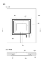
- both the active electrode E21 and the passive electrode E22 are formed in a plate shape. Further, the thickness of the active electrode E21 matches the thickness of the passive electrode E22. However, when the area of the main surface of the active electrode E21 is compared with the area of the main surface of the passive electrode E22, the area of the main surface of the passive electrode E22 is much larger than the area of the main surface of the active electrode E21.
- a rectangular opening OP wider than the main surface of the active electrode E21 is formed at the center of the main surface of the passive electrode E22.
- the passive electrode E22 is further formed with a strip-shaped cutout CT that reaches the outer edge of the passive electrode E22 from the opening OP.
- the direction of the one main surface of the active electrode E21 coincides with the direction of the one main surface of the passive electrode E22, and the direction of the other main surface of the active electrode E21 coincides with the direction of the other main surface of the passive electrode E22.
- one main surface of each of the active electrode E21 and the passive electrode E22 corresponds to the upper surface
- the other main surface of each of the active electrode E21 and the passive electrode E22 corresponds to the lower surface.
- the active electrode E21 is housed inside the opening OP such that the long side forming the main surface thereof extends in parallel with the long side forming the main surface of the opening OP.
- the antenna coil 40 is formed so as to draw a spiral with an axis extending in the vertical direction about the center of the opening OP.
- the spiral is drawn outside the opening OP, and the opening that appears when the spiral is viewed from above is wider than the opening OP.
- the active electrode E21 is formed on one main surface of the transparent sheet RS, and the passive electrode E22 and the antenna coil 40 are formed inside the transparent sheet RS.
- the antenna coil 40 is formed below the passive electrode E22. That is, the passive electrode E22 is provided at a position lower than the active electrode E21, and the antenna coil 40 is provided at a position lower than the passive electrode E22.
- the passive electrode E22 may be provided at the same height as the active electrode E21.
- the area of the main surface of the magnetic sheet MG is smaller than the area of the main surface of the passive electrode E22, it is larger than the area of the opening OP. Therefore, when viewed from below, the antenna coil 40 is covered with the magnetic sheet MG.
- the transparent sheet RS and the magnetic sheet MG are accommodated in the housing RHS such that one main surface of the transparent sheet RS is in contact with the back side of the one main surface of the housing RHS.
- the passive electrode E22 for electric field coupling is opened when the switch SW22 is turned off during wireless communication, and functions as a booster antenna that is magnetically coupled to the antenna coil 40. This ensures high wireless communication performance even with a small size.
- the switch SW21 is provided between the active electrode E21 and one end of the primary coil L3, and the switch SW22 is provided between the passive electrode E22 and the other end of the primary coil L3.
- the switch SW21 may be omitted, and the active electrode E21 and one end of the primary coil L3 may be directly connected.
- the switch SW22 may be omitted and the passive electrode E22 and the other end of the primary coil L3 may be directly connected. Further, both the switches SW21 and SW22 may be omitted.
- the power transmission system 100 of another embodiment is the same as that of the embodiment of FIGS. 1 to 5 except that a part of the configuration of the power receiving apparatus 30 is different from the power receiving apparatus 30 shown in FIG. Therefore, the duplicate description regarding the same configuration is omitted.
- passive electrodes E22_1 and E22_2 are provided instead of the passive electrode E22, and the switch SW22 is commonly connected to the passive electrodes E22_1 and E22_2.
- active electrode E21 is provided at the center of one main surface of housing RHS.
- the passive electrodes E22_1 and E22_2 are provided on the one main surface of the housing RHS so as to sandwich the active electrode E21 in a direction along the long side of the rectangle forming the one main surface of the housing RHS.
- the active electrode E21 and the passive electrodes E22_1 to E22_2 are housed in the housing RHS in a state in which one main surface thereof is adhered to the back side of the one main surface of the housing RHS.
- the direction of the one main surface of the magnetic sheet MG matches the direction of the one main surface of the housing RHS, and a part of the antenna coil 40 and the passive electrode E22_2 is viewed from above. It is stored in the housing RHS so as to overlap. Since one main surface of the passive electrode E22_2 is attached to the back side of the one main surface of the housing RHS, the antenna coil 40 is disposed at a position lower than the passive electrode E22_2.
- the electric field coupling passive electrodes E22_1 and E22_2 are opened by turning off the switch SW22 during wireless communication.
- the passive electrode E22_2 functions as a booster antenna that is magnetically coupled to the antenna coil 40 during wireless communication. This ensures high wireless communication performance even with a small size.
- the active electrode E21 and the passive electrodes E22_1 to E22_2 are attached to the back side of one main surface of the housing RHS, and the power receiving module on which the power receiving circuit 32, the RF circuit 42, and the CPU 44 are mounted.
- the RMD and the antenna coil 40 formed on the magnetic sheet MG are accommodated in the housing RHS.
- a resin electrode sheet RS on which the active electrode E21, the passive electrodes E22_1 to E22_2, the antenna coil 40, and the magnetic sheet MG are formed is manufactured, and the power receiving circuit 32, RF An external power receiving module unit RMDU mounted with the circuit 42 and the RF-IC 43 is manufactured, and the electrode sheet RS is attached to one main surface of the housing RHS, and the power receiving module unit RMDU is detachable from the housing RHS. You may make it wear.
- the antenna coil 40 is housed in the housing RHS so that a part of the antenna coil 40 overlaps with the passive electrode E22_2 when viewed from above the housing RHS.
- the antenna coil 40 may be housed in the housing RHS so that a part of the antenna coil 40 overlaps with both the passive electrodes E22_1 and E22_2 when viewed from above the housing RHS.
- a part of the antenna coil 40 may overlap with the active electrode E21.
- the antenna coil 40 is formed or arranged in the manner shown in FIG.
- the active electrode E21 and the passive electrodes E22_1 to E22_2 are provided on the back side of one main surface of the housing RHS.
- the active electrode E21 is provided at the center of the one long side surface of the housing RHS
- the passive electrode E22_1 is provided at a position extending from the other main surface of the housing RHS to the one long side surface and the other long side surface.
- the passive electrode E22_2 may be provided at a position extending from one main surface of the housing RHS to one long side surface and the other long side surface.
- the antenna coil 40 is mounted on the power receiving module RMD so as to be wound around the magnetic body MB and so that the winding axis is orthogonal to the long side surface of the housing RHS. Further, a part of the antenna coil 40 overlaps with both of the passive electrodes E22_1 and E22_2 when viewed from above the one long side surface of the housing RHS (see FIGS. 14A to 14B).
- the power transmission system 100 includes a configuration common to the power transmission system 100 illustrated in FIG. 1, and thus a common reference number is assigned to the common configuration.
- the antenna coil 40 is larger than the antenna coil 26.
- the power transmission device 10 includes a power transmission device 10 that transmits a high-frequency voltage of 100 kHz to 10 MHz by an electric field coupling method, and a power reception device 30 that receives a high-frequency voltage transmitted from the power transmission device 10 by an electric field coupling method.
- the power transmission device 10 and the power reception device 30 have a wireless communication function for communicating a high frequency signal of 13.56 MHz.
- a high frequency voltage to be transmitted is generated by the power transmission circuit 14, and a high frequency signal is input / output by the RF-IC 23 and the RF circuit 24 under the control of the CPU 22.
- the received high frequency voltage is converted into a DC voltage by the power receiving circuit 32, and the high frequency signal is input / output by the RF-IC 43 and the RF circuit 42 under the control of the CPU 44.
- the control circuit 16 provided in the power transmission circuit 14 gives a PWM signal having a frequency of 100 kHz to 10 MHz to the drive circuit 18.
- the drive circuit 18 converts the DC voltage supplied from the DC power supply 12 into a high frequency voltage according to the PWM signal supplied from the control circuit 16.
- the frequency of the converted high-frequency voltage matches the frequency of the PWM signal, and the level of the converted high-frequency voltage depends on the duty ratio of the PWM signal.
- the converted high-frequency voltage is applied to the primary winding L1 that forms the step-up transformer 20.
- the secondary winding L2 forming the step-up transformer 20 is excited with a high-frequency voltage boosted to a different voltage depending on the transformation ratio.
- One end of the secondary winding L2 is connected to an active electrode (small electrode) E11 for electric field coupling via a switch SW11, and the other end of the secondary winding L2 is a passive electrode (large electrode) E12_1 via a switch SW12. And E12_2.
- the switches SW11 and SW12 are turned on by the CPU 22 at times other than during wireless communication. Therefore, the high-frequency voltage boosted by the step-up transformer 20 for power transmission is applied to the active electrode E11 via the switch SW11 and to the passive electrodes E12_1 to E12_2 via the switch SW12.
- the power receiving device 30 is provided with an active electrode E21 and a passive electrode E22 for electric field coupling.
- the active electrode E21 and the passive electrode E22 are connected to one end and the other end of the primary winding L3 that form the step-down transformer 34 together with the secondary winding L4.
- the rectifying / smoothing circuit 36 rectifies and smoothes the high-frequency voltage excited by the secondary coil L4.
- the DC-DC converter 38 adjusts the level of the DC voltage generated thereby, and supplies the DC voltage having the adjusted level to the mobile device 46.
- the CPU 22 provided in the power transmission device 10 turns off the switches SW1 and SW2 when performing wireless communication with the power reception device 30.
- the passive electrode E12_2 functions as a booster antenna that is magnetically coupled to the antenna coil 26.
- the RF-IC 23 gives a baseband signal to the RF circuit 24 in order to perform wireless communication with the power receiving device 30.
- the RF circuit 24 modulates the supplied baseband signal into a high frequency signal, and transmits the modulated high frequency signal through the antenna coil 26 and the passive electrode E12_2.
- the transmitted high frequency signal is input to the RF circuit 42 via the antenna coil 40 provided in the power receiving device 30.
- the RF circuit 42 demodulates the input high-frequency signal into a baseband signal, and gives the demodulated baseband signal to the RF-IC 43.
- the baseband signal output from the RF-IC 43 is modulated into a high frequency signal by the RF circuit 42, and the modulated high frequency signal is transmitted through the antenna coil 40.
- the transmitted high frequency signal is input to the RF circuit 24 via the antenna coil 26 of the power transmission device 10 and demodulated into a baseband signal.
- the demodulated burst band signal is supplied to the RF-IC 23.
- the CPU 22 executes a process according to the flowchart shown in FIG. First, the switch SW11 is turned on in step S21, and the switch SW12 is turned on in step S23. In step S25, it is repeatedly determined whether or not wireless communication is started. When the determination result is updated from NO to YES, the switch SW11 is turned off in step S27, and the switch SW12 is turned off in step S29. In step S31, it is repeatedly determined whether or not the wireless communication is terminated, and when the determination result is updated from NO to YES, the process returns to step S21.
- step S21 and step S23 may be reversed or may be performed simultaneously.
- Steps S27 and S29 may also be reversed or performed simultaneously.
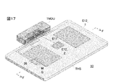
- power transmission device 10 includes a plate-shaped or rectangular parallelepiped housing THS in which one main surface and the other main surface each form a rectangle.
- a power transmission module unit TMDU on which the power transmission circuit 14, the CPU 22, the RF-IC 23, and the RF circuit 24 are mounted is detachably attached to the housing THS. Note that one main surface of the housing THS corresponds to the upper surface, and the other main surface of the housing RHS corresponds to the lower surface.
- the active electrode E11 and the passive electrodes E12_1 to E12_2 all have a common thickness and are formed in a plate shape. However, although the area of the main surface of the passive electrode E12_1 and the area of the main surface of the passive electrode E12_2 are common to each other, the area of the main surface of the active electrode E11 is much larger than the areas of the main surfaces of the passive electrodes E12_1 and E12_2. small.
- the active electrode E11 is provided at the center of one main surface of the housing THS.
- the passive electrodes E12_1 and E12_2 are provided on the one main surface of the housing THS so as to sandwich the active electrode E11 in a direction along the long side of the rectangle forming the one main surface of the housing RHS.
- the active electrode E11 and the passive electrodes E12_1 to E12_2 are arranged at the same height.
- the direction of the one main surface of the magnetic sheet MG matches the direction of the one main surface of the housing THS, and a part of the antenna coil 26 is connected to the passive electrode E12_2 when viewed from above. It is stored in the housing THS so as to overlap.
- the antenna coil 22 is disposed at a position lower than the passive electrode E12_2.
- the passive electrode E12_2 for electric field coupling is opened when the switch SW12 is turned off during wireless communication, and functions as a booster antenna that is magnetically coupled to the antenna coil 20.
- the passive electrode E12_2 for electric field coupling is opened when the switch SW12 is turned off during wireless communication, and functions as a booster antenna that is magnetically coupled to the antenna coil 20.
- the switch SW11 is provided between the active electrode E11 and one end of the secondary coil L2, and the switch SW12 is provided between each of the passive electrodes E12_1 and E12_2 and the other end of the secondary coil L2.
- the switch SW11 may be omitted and the active electrode E11 and one end of the secondary coil L2 may be directly connected.
- the switch SW12 may be omitted and the passive electrodes E12_1 and E12_2 may be directly connected to the other end of the secondary coil L2.
- both the switches SW21 and SW22 may be omitted.
Landscapes
- Engineering & Computer Science (AREA)
- Computer Networks & Wireless Communication (AREA)
- Power Engineering (AREA)
- Signal Processing (AREA)
- Near-Field Transmission Systems (AREA)
- Charge And Discharge Circuits For Batteries Or The Like (AREA)
Abstract
Description
16 …制御回路
20 …昇圧トランス
24,42 …RF回路
26,40 …アンテナコイル
30 …受電装置
36 …降圧トランス
44 …CPU
100 …電力伝送システム
Claims (10)
- 無線通信用の給電コイル、
無線ICチップと給電回路とを備え、前記給電コイルを介して高周波信号の送受信を行う近距離無線通信手段、
送電装置と電界結合する第1電極、
前記送電装置との無線通信時に前記給電コイルと磁界結合するブースターアンテナとして機能し、前記送電装置からの受電時に前記第1電極と協働して前記送電装置と電界結合する第2電極として機能する導電体、および
電界結合によって前記第1電極および前記導電体に励起された交流電圧に基づく電力を負荷に供給する供給手段を備える、受電装置。 - 前記供給手段は、前記第1電極および前記導電体に励起された交流電圧を降圧する降圧手段、および前記降圧手段によって降圧された交流電圧を整流する整流手段を含む、請求項1記載の受電装置。
- 無線通信時に前記第1電極および前記導電体の少なくとも一方と前記供給手段との接続を遮断する遮断手段をさらに備える、請求項1または2記載の受電装置。
- 前記第1電極の面積は前記第2電極の面積よりも小さい、請求項1ないし3のいずれかに記載の受電装置。
- 前記送電装置に面する受電面をさらに備え、
前記受電面に対して、前記導電体は前記第1電極と同じ距離または前記第1電極よりも遠い距離に設けられ、前記給電コイルは前記導電体よりも遠い距離に設けられる、請求項1ないし4のいずれかに記載の受電装置。 - 前記導電体は前記第1電極を囲むように配置される、請求項1ないし5のいずれかに記載の受電装置。
- 前記給電コイルは平面コイルであり、そのコイル開口が前記受電面に対して対向するように配置されるとともに、前記給電コイルの前記受電面から遠い側の面に設けられた磁性体をさらに備える、請求項1ないし6のいずれかに記載の受電装置。
- 無線通信用の給電コイル、
無線ICチップと給電回路とを備え、前記給電コイルを介して高周波信号の送受信を行う近距離無線通信手段、
受電装置と電界結合する第1電極、
前記受電装置との無線通信時に前記給電コイルと磁界結合するブースターアンテナとして機能し、前記受電装置への送電時に前記第1電極と協働して前記受電装置と電界結合する第2電極として機能する導電体、および
交流電圧源から出力された交流電圧を前記第1電極および前記導電体に供給する供給手段を備える、送電装置。 - 電界結合方式で交流電圧を送電する送電装置、および前記送電装置から送電された交流電圧を前記電界結合方式で受電する受電装置を備える電力伝送システムであって、
前記受電装置は、
無線通信用の給電コイル、
無線ICチップと給電回路とを備え、前記給電コイルを介して高周波信号の送受信を行う近距離無線通信手段、
前記送電装置と電界結合する第1電極、
前記送電装置との無線通信時に前記給電コイルと磁界結合するブースターアンテナとして機能し、前記送電装置からの受電時に前記第1電極と協働して前記送電装置と電界結合する第2電極として機能する導電体、および
電界結合によって前記第1電極および前記導電体に励起された交流電圧に基づく電力を負荷に供給する供給手段を備える、電力伝送システム。 - 電界結合方式で交流電圧を送電する送電装置、および前記送電装置から送電された交流電圧を前記電界結合方式で受電する受電装置を備える電力伝送システムであって、
前記送電装置は、
無線通信用の給電コイル、
無線ICチップと給電回路とを備え、前記給電コイルを介して高周波信号の送受信を行う近距離無線通信手段、
前記受電装置と電界結合する第1電極、
前記受電装置との無線通信時に前記給電コイルと磁界結合するブースターアンテナとして機能し、前記受電装置への送電時に前記第1電極と協働して前記受電装置と電界結合する第2電極として機能する導電体、および
交流電圧源から出力された交流電圧を前記第1電極および前記導電体に供給する供給手段を備える、電力伝送システム。
Priority Applications (4)
| Application Number | Priority Date | Filing Date | Title |
|---|---|---|---|
| JP2014557314A JP5737545B2 (ja) | 2013-01-21 | 2013-08-30 | 受電装置、送電装置および電力伝送システム |
| CN201390000805.5U CN204696809U (zh) | 2013-01-21 | 2013-08-30 | 受电装置、送电装置及电力输送系统 |
| GB1504383.9A GB2519924A (en) | 2013-01-21 | 2013-08-30 | Power receiving device, power transmitting device, and power transmission system |
| US14/719,417 US9780839B2 (en) | 2013-01-21 | 2015-05-22 | Power reception device, power transmission device, and power transmission system |
Applications Claiming Priority (2)
| Application Number | Priority Date | Filing Date | Title |
|---|---|---|---|
| JP2013-008082 | 2013-01-21 | ||
| JP2013008082 | 2013-01-21 |
Related Child Applications (1)
| Application Number | Title | Priority Date | Filing Date |
|---|---|---|---|
| US14/719,417 Continuation US9780839B2 (en) | 2013-01-21 | 2015-05-22 | Power reception device, power transmission device, and power transmission system |
Publications (1)
| Publication Number | Publication Date |
|---|---|
| WO2014112150A1 true WO2014112150A1 (ja) | 2014-07-24 |
Family
ID=51209264
Family Applications (1)
| Application Number | Title | Priority Date | Filing Date |
|---|---|---|---|
| PCT/JP2013/073317 Ceased WO2014112150A1 (ja) | 2013-01-21 | 2013-08-30 | 受電装置、送電装置および電力伝送システム |
Country Status (5)
| Country | Link |
|---|---|
| US (1) | US9780839B2 (ja) |
| JP (1) | JP5737545B2 (ja) |
| CN (1) | CN204696809U (ja) |
| GB (1) | GB2519924A (ja) |
| WO (1) | WO2014112150A1 (ja) |
Cited By (6)
| Publication number | Priority date | Publication date | Assignee | Title |
|---|---|---|---|---|
| CN104319740A (zh) * | 2014-10-14 | 2015-01-28 | 江苏嘉钰新能源技术有限公司 | 一种电场耦合无线充电系统的监测与保护装置及其方法 |
| WO2017014009A1 (ja) * | 2015-07-22 | 2017-01-26 | デクセリアルズ株式会社 | アンテナ装置 |
| WO2017014010A1 (ja) * | 2015-07-22 | 2017-01-26 | デクセリアルズ株式会社 | アンテナ装置、及び電子機器 |
| JP2017139724A (ja) * | 2015-08-21 | 2017-08-10 | 矢崎総業株式会社 | 電力伝送通信ユニット及び電力伝送通信装置 |
| JP2018108012A (ja) * | 2016-12-22 | 2018-07-05 | パナソニックIpマネジメント株式会社 | 移動体および無線電力伝送システム |
| US10396464B2 (en) | 2015-08-21 | 2019-08-27 | Yazaki Corporation | Power transmitting communication unit and power transmitting communication device |
Families Citing this family (9)
| Publication number | Priority date | Publication date | Assignee | Title |
|---|---|---|---|---|
| JP6127777B2 (ja) * | 2013-06-28 | 2017-05-17 | ソニー株式会社 | 給電装置および給電システム |
| KR20160104403A (ko) * | 2015-02-26 | 2016-09-05 | 삼성전자주식회사 | 무선 충전 방법 및 그 전자 장치 |
| US20170005395A1 (en) * | 2015-06-30 | 2017-01-05 | Tdk Corporation | Antenna device |
| JP6643152B2 (ja) * | 2016-03-09 | 2020-02-12 | 京セラ株式会社 | 電子機器 |
| US10097030B2 (en) * | 2016-04-29 | 2018-10-09 | Taiwan Semiconductor Manufacturing Co., Ltd | Packaged semiconductor devices with wireless charging means |
| US11139686B2 (en) | 2017-04-13 | 2021-10-05 | Richard Marion Mansell | System and method for wireless transmission of power |
| WO2019168416A1 (en) | 2018-03-02 | 2019-09-06 | Auckland Uniservices Limited | A wireless power transfer device |
| CN109245329B (zh) * | 2018-09-06 | 2021-10-26 | 华南理工大学 | 一种基于矢量功率叠加的无线能量传输系统及方法 |
| US20220224159A1 (en) * | 2019-04-26 | 2022-07-14 | Panasonic Intellectual Property Management Co., Ltd. | Wireless power and data transmission apparatus and transmission module |
Citations (2)
| Publication number | Priority date | Publication date | Assignee | Title |
|---|---|---|---|---|
| JPH07134894A (ja) * | 1993-11-10 | 1995-05-23 | Nec Corp | 半導体記憶装置 |
| JPH11513518A (ja) * | 1995-10-11 | 1999-11-16 | モトローラ・インコーポレイテッド | 遠隔給電される電子タッグの励起装置/読取装置およびその方法 |
Family Cites Families (7)
| Publication number | Priority date | Publication date | Assignee | Title |
|---|---|---|---|---|
| US6040773A (en) | 1995-10-11 | 2000-03-21 | Motorola, Inc. | Radio frequency identification tag arranged for magnetically storing tag state information |
| CN101416411B (zh) | 2006-03-21 | 2013-05-15 | 株式会社村田制作所 | 通过穿越电介质的局部感应传输能量的装置 |
| EP2424041B1 (en) | 2009-04-21 | 2018-11-21 | Murata Manufacturing Co., Ltd. | Antenna apparatus and resonant frequency setting method of same |
| JP5376060B2 (ja) * | 2010-07-08 | 2013-12-25 | 株式会社村田製作所 | アンテナ及びrfidデバイス |
| JP5609922B2 (ja) * | 2011-08-10 | 2014-10-22 | 株式会社村田製作所 | アンテナ装置および通信端末装置 |
| JP5737426B2 (ja) * | 2011-11-14 | 2015-06-17 | 株式会社村田製作所 | アンテナ装置及び無線通信装置 |
| DE102011056323A1 (de) * | 2011-12-13 | 2013-06-13 | Infineon Technologies Ag | Booster-Antennenstruktur für eine Chipkarte |
-
2013
- 2013-08-30 GB GB1504383.9A patent/GB2519924A/en not_active Withdrawn
- 2013-08-30 WO PCT/JP2013/073317 patent/WO2014112150A1/ja not_active Ceased
- 2013-08-30 JP JP2014557314A patent/JP5737545B2/ja not_active Expired - Fee Related
- 2013-08-30 CN CN201390000805.5U patent/CN204696809U/zh not_active Expired - Lifetime
-
2015
- 2015-05-22 US US14/719,417 patent/US9780839B2/en not_active Expired - Fee Related
Patent Citations (2)
| Publication number | Priority date | Publication date | Assignee | Title |
|---|---|---|---|---|
| JPH07134894A (ja) * | 1993-11-10 | 1995-05-23 | Nec Corp | 半導体記憶装置 |
| JPH11513518A (ja) * | 1995-10-11 | 1999-11-16 | モトローラ・インコーポレイテッド | 遠隔給電される電子タッグの励起装置/読取装置およびその方法 |
Cited By (12)
| Publication number | Priority date | Publication date | Assignee | Title |
|---|---|---|---|---|
| CN104319740A (zh) * | 2014-10-14 | 2015-01-28 | 江苏嘉钰新能源技术有限公司 | 一种电场耦合无线充电系统的监测与保护装置及其方法 |
| WO2017014009A1 (ja) * | 2015-07-22 | 2017-01-26 | デクセリアルズ株式会社 | アンテナ装置 |
| WO2017014010A1 (ja) * | 2015-07-22 | 2017-01-26 | デクセリアルズ株式会社 | アンテナ装置、及び電子機器 |
| JP2017028482A (ja) * | 2015-07-22 | 2017-02-02 | デクセリアルズ株式会社 | アンテナ装置 |
| JP2017028483A (ja) * | 2015-07-22 | 2017-02-02 | デクセリアルズ株式会社 | アンテナ装置、及び電子機器 |
| CN107851898A (zh) * | 2015-07-22 | 2018-03-27 | 迪睿合株式会社 | 天线装置 |
| CN107851899A (zh) * | 2015-07-22 | 2018-03-27 | 迪睿合株式会社 | 天线装置及电子设备 |
| US10936931B2 (en) | 2015-07-22 | 2021-03-02 | Dexerials Corporation | Antenna device |
| US10936934B2 (en) | 2015-07-22 | 2021-03-02 | Dexerials Corporation | Antenna device and electronic apparatus |
| JP2017139724A (ja) * | 2015-08-21 | 2017-08-10 | 矢崎総業株式会社 | 電力伝送通信ユニット及び電力伝送通信装置 |
| US10396464B2 (en) | 2015-08-21 | 2019-08-27 | Yazaki Corporation | Power transmitting communication unit and power transmitting communication device |
| JP2018108012A (ja) * | 2016-12-22 | 2018-07-05 | パナソニックIpマネジメント株式会社 | 移動体および無線電力伝送システム |
Also Published As
| Publication number | Publication date |
|---|---|
| CN204696809U (zh) | 2015-10-07 |
| US9780839B2 (en) | 2017-10-03 |
| JP5737545B2 (ja) | 2015-06-17 |
| GB201504383D0 (en) | 2015-04-29 |
| JPWO2014112150A1 (ja) | 2017-01-19 |
| GB2519924A (en) | 2015-05-06 |
| US20150256228A1 (en) | 2015-09-10 |
Similar Documents
| Publication | Publication Date | Title |
|---|---|---|
| JP5737545B2 (ja) | 受電装置、送電装置および電力伝送システム | |
| US9496082B2 (en) | Coil substrate for wireless charging and electric device using the same | |
| US8421574B2 (en) | Contactless power transmission apparatus and a method of manufacturing a secondary side thereof | |
| JP4911148B2 (ja) | 非接触給電装置 | |
| KR101890326B1 (ko) | 무선전력 전송모듈 및 이를 포함하는 휴대용 보조배터리 | |
| CN104756361B (zh) | 电力传输系统 | |
| US8970069B2 (en) | Wireless power receiver and wireless power transmission system | |
| CN109155526B (zh) | 无线可再充电蓄能器 | |
| CN105814772A (zh) | 混合式无线电力传输系统及其方法 | |
| WO2018021060A1 (ja) | 無線モジュール、rfidシステムおよびワイヤレス給電装置 | |
| JP2019530408A (ja) | 無線電力伝送装置、無線電力送信システム、及び無線電力送信システムを駆動する方法 | |
| WO2013150784A1 (ja) | コイルユニット及びコイルユニットを備える電力伝送装置 | |
| JP5804254B2 (ja) | アンテナ | |
| JP6252051B2 (ja) | 電力変換器 | |
| JPWO2020066081A1 (ja) | ワイヤレス給電システム | |
| JP2009224959A (ja) | 電子回路、無線端末および無線端末システム | |
| JP6040510B2 (ja) | 電力伝送システム | |
| JP5737546B2 (ja) | 受電装置、送電装置および電力伝送システム | |
| JP2012095505A (ja) | ワイヤレス電力伝送システムおよび送電装置 | |
| JP2014093797A (ja) | 電力伝送システム | |
| JP2013074683A (ja) | アンテナ | |
| KR102040726B1 (ko) | 무선 전력 전송을 위한 공진 장치 | |
| JP2014093320A (ja) | 電力伝送システム | |
| JP2014093321A (ja) | 電力伝送システム | |
| WO2019210503A1 (zh) | 可实现能量漏斗效应的无线充电系统及其无线充电方法 |
Legal Events
| Date | Code | Title | Description |
|---|---|---|---|
| WWE | Wipo information: entry into national phase |
Ref document number: 201390000805.5 Country of ref document: CN |
|
| 121 | Ep: the epo has been informed by wipo that ep was designated in this application |
Ref document number: 13872133 Country of ref document: EP Kind code of ref document: A1 |
|
| ENP | Entry into the national phase |
Ref document number: 2014557314 Country of ref document: JP Kind code of ref document: A |
|
| ENP | Entry into the national phase |
Ref document number: 1504383 Country of ref document: GB Kind code of ref document: A Free format text: PCT FILING DATE = 20130830 |
|
| WWE | Wipo information: entry into national phase |
Ref document number: 1504383.9 Country of ref document: GB |
|
| NENP | Non-entry into the national phase |
Ref country code: DE |
|
| 122 | Ep: pct application non-entry in european phase |
Ref document number: 13872133 Country of ref document: EP Kind code of ref document: A1 |