WO2014109211A1 - 電子・電気機器用銅合金、電子・電気機器用部品及び端子 - Google Patents
電子・電気機器用銅合金、電子・電気機器用部品及び端子 Download PDFInfo
- Publication number
- WO2014109211A1 WO2014109211A1 PCT/JP2013/084251 JP2013084251W WO2014109211A1 WO 2014109211 A1 WO2014109211 A1 WO 2014109211A1 JP 2013084251 W JP2013084251 W JP 2013084251W WO 2014109211 A1 WO2014109211 A1 WO 2014109211A1
- Authority
- WO
- WIPO (PCT)
- Prior art keywords
- mass
- electronic
- phase
- content
- less
- Prior art date
- Legal status (The legal status is an assumption and is not a legal conclusion. Google has not performed a legal analysis and makes no representation as to the accuracy of the status listed.)
- Ceased
Links
Images


Classifications
-
- H—ELECTRICITY
- H01—ELECTRIC ELEMENTS
- H01B—CABLES; CONDUCTORS; INSULATORS; SELECTION OF MATERIALS FOR THEIR CONDUCTIVE, INSULATING OR DIELECTRIC PROPERTIES
- H01B1/00—Conductors or conductive bodies characterised by the conductive materials; Selection of materials as conductors
- H01B1/02—Conductors or conductive bodies characterised by the conductive materials; Selection of materials as conductors mainly consisting of metals or alloys
- H01B1/026—Alloys based on copper
-
- C—CHEMISTRY; METALLURGY
- C22—METALLURGY; FERROUS OR NON-FERROUS ALLOYS; TREATMENT OF ALLOYS OR NON-FERROUS METALS
- C22C—ALLOYS
- C22C9/00—Alloys based on copper
-
- C—CHEMISTRY; METALLURGY
- C22—METALLURGY; FERROUS OR NON-FERROUS ALLOYS; TREATMENT OF ALLOYS OR NON-FERROUS METALS
- C22F—CHANGING THE PHYSICAL STRUCTURE OF NON-FERROUS METALS AND NON-FERROUS ALLOYS
- C22F1/00—Changing the physical structure of non-ferrous metals or alloys by heat treatment or by hot or cold working
-
- C—CHEMISTRY; METALLURGY
- C22—METALLURGY; FERROUS OR NON-FERROUS ALLOYS; TREATMENT OF ALLOYS OR NON-FERROUS METALS
- C22F—CHANGING THE PHYSICAL STRUCTURE OF NON-FERROUS METALS AND NON-FERROUS ALLOYS
- C22F1/00—Changing the physical structure of non-ferrous metals or alloys by heat treatment or by hot or cold working
- C22F1/08—Changing the physical structure of non-ferrous metals or alloys by heat treatment or by hot or cold working of copper or alloys based thereon
Definitions
- the present invention relates to a copper alloy for electronic / electric equipment used as a component for electronic / electric equipment such as a connector of a semiconductor device, other terminals, a movable conductive piece of an electromagnetic relay, and a lead frame, and electronic / electric using the same It relates to equipment parts and terminals.
- CDA alloy no. C15100 (Cu—Zr alloy) is used.
- This Cu—Zr alloy is a precipitation hardening type copper alloy, has improved strength while maintaining a high conductivity of about 90% IACS, and is also excellent in heat resistance.
- the Cu—Zr alloy has a composition close to that of pure copper in order to ensure high electrical conductivity, has high ductility, and has poor shear workability. More specifically, there has been a problem that when press punching is performed, burrs are generated and punching cannot be performed with high dimensional accuracy. Further, there are problems such as wear of molds and generation of punching scraps.
- Patent Document 1 the addition of elements such as Pb, Bi, Ca, Sr, Ba, and Te to the Cu—Zr-based alloy simultaneously shears while maintaining high conductivity. It was insufficient for improving the workability. Further, since elements such as Pb, Bi, and Te are low melting point metals, there is a possibility that hot workability is significantly deteriorated.
- the method disclosed in Patent Document 2 relates to a Cu—Cr—Si—Zn—Sn alloy, and improves shear workability even when applied to a Cu—Zr alloy having a different alloy system as it is. I could't. Furthermore, as disclosed in Patent Document 3, it is conceivable to improve the shear workability by dispersing the oxide particles.
- the present invention has been made against the background as described above, and has a particularly high electrical conductivity and excellent shear workability, and is suitable for electronic terminals such as connectors and electronic / electric parts such as relays. It is an object of the present invention to provide a copper alloy for electronic / electric equipment made of an alloy, and a component and terminal for electronic / electric equipment made of the copper alloy for electronic / electric equipment.
- the present inventors have conducted intensive research. As a result, by adding a small amount of Ca to the Cu—Zr alloy and optimizing the production conditions, the present inventors have made 2 of Cu, Zr, and Ca. The phase particles were dispersed in the matrix, and it was found that the shear workability can be greatly improved while maintaining high electrical conductivity.
- the copper alloy for electronic / electric equipment of the present invention has a Zr content of 0.05 mass% to 0.15 mass% and a Ca content of 0. 0.001 mass% or more and less than 0.08 mass%, Pb content is less than 0.05 mass%, Bi content is less than 0.01 mass%, and the balance is composed of Cu and inevitable impurities,
- the ratio Zr / Ca between the content (mass%) and the Ca content (mass%) is 1.2 or more, and a phase mainly composed of Cu and Zr and a phase mainly composed of Cu and Ca And two-phase particles composed of two phases, and single-phase particles composed of one phase mainly composed of Cu and Zr, and having a conductivity exceeding 88% IACS. .
- the copper alloy for electronic / electric equipment having the above-described configuration, it has two-phase particles composed of two phases of a phase mainly composed of Cu and Zr and a phase mainly composed of Cu and Ca.
- the shearing process represented by press punching or the like is performed, the two-phase particles serve as a starting point for fracture, and the shearing workability is greatly improved.
- single-phase particles composed of one phase mainly composed of Cu and Zr are precipitated, the strength can be improved by precipitation hardening, and the shear workability can be improved.
- the content of Zr is 0.05 mass% or more, the above-mentioned two-phase particles and single-phase particles can be sufficiently dispersed, and improvement of shear workability and strength can be achieved. it can.
- the content of Zr is 0.15 mass% or less, it is possible to suppress a decrease in conductivity and to uniformly disperse precipitates by surely forming a solution of Zr. Can be made.
- the Zr content is in the range of 0.06 mass% to 0.14 mass%.
- the Ca content is 0.001 mass% or more, the above-described two-phase particles can be reliably dispersed, and the shear workability can be improved.
- the Ca content is less than 0.08 mass%, workability can be ensured, and the occurrence of defects such as disconnection and cracking in hot processing and cold processing after casting can be suppressed.
- it is preferable that the Ca content is in the range of 0.002 mass% to 0.03 mass%.
- the ratio Zr / Ca of the Zr content (mass%) and the Ca content (mass%) is 1.2 or more, the phase mainly composed of Cu and Zr, Cu and Ca are contained. It is possible to reliably disperse not only two-phase particles composed of two phases as main components but also single-phase particles composed of one phase mainly composed of Cu and Zr.
- the Pb content is less than 0.05 mass% (500 ppm) and the Bi content is less than 0.01 mass% (100 ppm), the grain boundary strength due to segregation of the low melting point metals Pb and Bi is reduced. Reduction can be suppressed and hot workability can be improved.
- the content of Pb and Bi is 0.001 mass% (10 ppm) or less, and further 0.0005 mass% (5 ppm) or less.
- the electrical conductivity exceeds 88% IACS, the above-mentioned single-phase particles are sufficiently precipitated in the matrix phase, and the strength can be reliably improved. Further, it can be used as a material for electronic / electrical parts that require particularly high electrical conductivity. In order to ensure that the above-described effects are achieved, it is preferable to set the conductivity to 89% IACS or higher, more preferably 90% IACS or higher.
- the two-phase particles have a phase composed of an intermetallic compound having a crystal structure of Cu 5 Zr or Cu 51 Zr 14 and a crystal structure of Cu 5 Ca. And a phase composed of an intermetallic compound.
- the two-phase particles crystallize in the parent phase of Cu, and the two-phase particles remain in the Cu even after the subsequent processing step, so that the shear workability can be improved reliably. It becomes possible.
- the S content is 0.0005 mass% or less and the O content is 0.0003 mass% or less. Since S reacts with Zr and Ca to form sulfides, and O reacts with Zr and Ca to form oxides, Zr and Ca are consumed. Therefore, by specifying the contents of S and O as described above, Zr and Ca necessary for forming the two-phase particles and the single-phase particles can be secured, and the improvement of the shear workability and the improvement of the strength are ensured. Can be achieved.
- the component for electronic / electrical equipment and the terminal of the present invention are characterized by comprising the above-mentioned copper alloy for electronic / electrical equipment.
- Components for electronic and electrical equipment with this configuration for example, terminals such as connectors, relays, lead frames), especially terminals such as connectors, are excellent in electrical conductivity, strength, and shear workability, so they have excellent dimensional accuracy and small size. Even if the thickness and thickness are reduced, excellent characteristics can be exhibited.
- a copper alloy for electronic and electrical equipment made of a Cu-Zr-based alloy having a particularly high conductivity and excellent shear workability, and suitable for electronic and electrical parts such as terminals such as connectors and relays, and It is possible to provide an electronic / electric equipment part and a terminal made of the copper alloy for electronic / electric equipment.
- the copper alloy for electronic and electric apparatuses which is one Embodiment of this invention is demonstrated.
- the copper alloy for electronic and electrical equipment has a Zr content of 0.05 mass% to 0.15 mass%, a Ca content of 0.001 mass% to less than 0.08 mass%, and a Pb content. Is less than 0.05 mass%, the Bi content is less than 0.01 mass%, the balance is composed of Cu and inevitable impurities, the Zr content (mass%) and the Ca content (mass%) Zr / Ca is 1.2 or more.
- the S content is regulated to 0.0005 mass% or less, and the O content is regulated to 0.0003 mass% or less.
- the copper alloy for electronic and electric devices which is this embodiment, it is comprised so that electrical conductivity may exceed 88% IACS.
- grains comprised by 1 phase which has Cu and Zr as a main component, the phase which has Cu and Zr as a main component, and Cu and Ca are included.
- the “main component” in the single-phase particles and the two-phase particles refers to the component having the largest content and the component having the second largest content.
- Cu and Zr are the largest or second largest component.
- the above-mentioned two-phase particles are composed of a phase composed of an intermetallic compound having a crystal structure of Cu 5 Zr or Cu 51 Zr 14 and an intermetallic compound having a crystal structure of Cu 5 Ca. Phase.
- an intermetallic compound having a crystal structure of Cu 5 Zr or Cu 51 Zr 14 and an intermetallic compound having a crystal structure of Cu 5 Ca. Phase.
- Zr 0.05 mass% or more and 0.15 mass% or less
- Zr is an element that has the effect of improving the strength by binding to Cu to form the above-mentioned single-phase particles and precipitating in the Cu matrix. Moreover, it is an element which has the effect of forming the above-mentioned two-phase particles and improving the shear workability by being added to Cu together with Ca.
- the content of Zr is less than 0.05 mass%, the effect cannot be sufficiently achieved.
- the content of Zr exceeds 0.15 mass%, the conductivity may be significantly lowered. For these reasons, the Zr content is set to 0.05 mass% or more and 0.15 mass% or less.
- Zr is an active element, it becomes an oxide, sulfide, or the like and is involved as inclusions, and there is a risk that defects such as disconnection or cracking may occur during subsequent processing. From the viewpoint of preventing such defects, it is preferable that the Zr content is in the range of 0.06 mass% to 0.14 mass%.
- Ca is an element having an effect of forming the above-mentioned two-phase particles and improving the shear workability by being added to Cu together with Zr.
- the content of Ca is less than 0.001 mass%, the effect cannot be sufficiently achieved.
- the Ca content is 0.08 mass% or more, disconnection or cracking may occur in hot and cold working after casting. For this reason, the Ca content is set to 0.001 mass% or more and less than 0.08 mass%.
- the Ca content is preferably within the range of 0.002 mass% to 0.03 mass%.
- Pb and Bi are elements that segregate at grain boundaries or the like as low melting point metals, and greatly deteriorate hot workability. Therefore, in this embodiment, hot workability is ensured by regulating the Pb content to less than 0.05 mass% and the Bi content to less than 0.01 mass%. In order to surely prevent the deterioration of hot workability, the content of Pb and Bi is preferably 0.001 mass% or less, more preferably 0.0005 mass% or less.
- S is an element that reacts with Zr and Ca to form a sulfide.
- O is an element that reacts with Zr and Ca to form an oxide. Therefore, when a large amount of S and O is present, Zr and Ca are consumed as sulfides and oxides, so that the above-mentioned two-phase particles and single-phase particles are insufficient, improving shear workability and improving strength. There is a risk that it will not be possible. Therefore, in this embodiment, the S content is regulated to less than 0.0005 mass%, and the O content is regulated to less than 0.0003 mass%.
- Inevitable impurities include, for example, Mg, Sn, Fe, Co, Al, Ag, Mn, B, P, Sr, Ba, Sc, Y, rare earth elements, Hf, V, Nb, Ta, Cr, Mo, W , Re, Ru, Os, Se, Te, Rh, Ir, Pd, Pt, Au, Zn, Cd, Ga, In, Li, Si, Ge, As, Sb, Ti, Tl, C, Ni, Be, N , H, Hg and the like. These inevitable impurities are desirably 0.3 mass% or less in total.
- the two-phase particles are particles crystallized in the parent phase of Cu in the casting step S02 described later.
- the two-phase particles are composed of two phases of a phase mainly composed of Cu and Zr and a phase mainly composed of Cu and Ca.
- Single phase particles are composed of an intermetallic compound containing Cu and Zr as main components. Single-phase particles are formed by precipitating Zr dissolved in a Cu matrix, and have the effect of improving strength while maintaining high electrical conductivity by precipitation hardening.
- (Dissolution step S01) First, Zr and Ca are added to the molten copper obtained by melting the copper raw material, and the components are adjusted to produce a molten copper alloy.
- Zr and Ca Zr alone, Ca alone, Cu—Zr master alloy, Cu—Ca master alloy, or the like can be used. Moreover, you may melt
- the molten copper is preferably so-called 4NCu having a purity of 99.99% by mass or more. Further, in the melting step, it is preferable to use a vacuum furnace or an atmosphere furnace having an inert gas atmosphere or a reducing atmosphere in order to suppress oxidation of active elements Zr and Ca.
- the copper alloy molten metal whose components are adjusted is poured into a mold to produce an ingot.
- the cooling rate at the time of solidification is set to less than 5 ° C./sec, preferably in the range of 0.1 ° C./sec to less than 5 ° C./sec.
- Heat treatment step S03 Next, heat treatment is performed for homogenization and solution of the obtained ingot.
- a heat treatment for heating the ingot to 800 ° C. or higher and 1080 ° C. or lower, Zr is uniformly diffused in the ingot or Zr is dissolved in the matrix.
- This heat treatment step S03 is preferably performed in a non-oxidizing or reducing atmosphere.
- the cooling method after a heating is not specifically limited, It is preferable to employ
- the two-phase particles crystallized in the casting step S02 are maintained as they are without being dissolved or diffused.
- Hot rolling process S04 hot rolling is performed in order to increase the efficiency of rough machining and make the structure uniform.
- the processing method is not particularly limited, but when the final shape is a plate or strip, it is preferable to employ rolling. It is preferable to employ extrusion or groove rolling in the case of a wire or bar, and forging or pressing in the case of a bulk shape.
- the temperature during hot working is also not particularly limited, but is preferably in the range of 500 ° C. or higher and 1050 ° C. or lower.
- the cooling method after hot rolling is not specifically limited, It is preferable to employ
- intermediate processing and intermediate heat treatment may be added for the purpose of thorough solution, recrystallization structure, or softening for improving workability.
- the temperature condition in the intermediate processing step is not particularly limited, but it is preferable to be within a range of ⁇ 200 ° C. to 200 ° C. which is cold or warm processing.
- the processing rate is appropriately selected so as to approximate the final shape, but is preferably set to 20% or more in order to reduce the number of intermediate heat treatment steps until the final shape is obtained. Moreover, it is more preferable that the processing rate is 30% or more.
- the plastic working method is not particularly limited, and for example, rolling, wire drawing, extrusion, groove rolling, forging, pressing, and the like can be employed.
- the method for the intermediate heat treatment is not particularly limited, but it is preferable to perform the heat treatment in a non-oxidizing atmosphere or a reducing atmosphere under conditions of 500 ° C. or higher and 1050 ° C. or lower. This intermediate processing and intermediate heat treatment step may be repeated.
- the temperature condition in the finishing step S05 is not particularly limited, but is preferably in the range of ⁇ 200 ° C. to 200 ° C.
- the processing rate is appropriately selected so as to approximate the final shape, but in order to improve the strength by work hardening, the processing rate is preferably set to 30% or more, and further improvement in strength is achieved. When aiming, it is more preferable that the processing rate is 50% or more.
- the processing method is not particularly limited, but when the final shape is a plate or strip, it is preferable to employ rolling. It is preferable to employ extrusion or groove rolling in the case of a wire or bar, and forging or pressing in the case of a bulk shape.
- the finish processing step S05 and the aging heat treatment step S06 described above may be repeatedly performed. In order to improve the strength, cold rolling may be applied at a processing rate of 10% to 70%. Furthermore, heat treatment may be performed for tempering, stress relaxation resistance, and removal of residual strain.
- the cooling method after the heat treatment is not particularly limited, but it is preferable to employ a method in which the cooling rate is 200 ° C./min or more, such as water quenching.
- a copper alloy for electrical and electronic equipment having a single-phase particle is produced.
- the copper alloy for electric / electronic devices according to the present embodiment as a raw material, punching or bending, etc., for example, terminals for connectors or the like, components for electronic / electric devices such as relays and lead frames are formed. .
- the copper alloy for electrical / electronic equipment configured as described above, it is composed of two phases of a phase mainly composed of Cu and Zr and a phase mainly composed of Cu and Ca. Since the two-phase particles are crystallized in the parent phase of Cu, when the shearing process such as press punching is performed, the two-phase particles become a starting point of fracture, and the shear workability is greatly improved. Therefore, it is possible to mold a small electronic / electric equipment part with high dimensional accuracy by stamping or the like.
- single-phase particles composed of one phase mainly composed of Cu and Zr are precipitated in the parent phase of Cu, it is possible to improve conductivity and strength. In addition, shear workability can be improved. In this embodiment, since the conductivity is configured to exceed 88% IACS, the above-described single-phase particles are sufficiently precipitated in the parent phase of Cu, and the strength is reliably improved. Is possible.
- the Zr content is set in the range of 0.05 mass% or more and 0.15 mass% or less, the above-described two-phase particles and single-phase particles are sufficiently dispersed to obtain shear workability. As well as improving the strength and strength, it is possible to suppress a decrease in conductivity. Therefore, it is possible to obtain a copper alloy for electrical and electronic equipment that is excellent in high electric power, strength, and shear workability.
- the Ca content is set within a range of 0.001 mass% or more and less than 0.08 mass%, the above-described two-phase particles can be reliably dispersed, and the shear workability can be improved. In addition, it is possible to ensure hot workability and cold workability. Furthermore, since the ratio Zr / Ca of the Zr content (mass%) and the Ca content (mass%) is 1.2 or more, not only two-phase particles but also Cu and Zr as main components. The single phase particles to be deposited can be surely precipitated, and the strength can be improved.
- the Pb content is less than 0.05 mass% and the Bi content is less than 0.01 mass%, hot workability can be ensured. Furthermore, since the S content is 0.0005 mass% or less and the O content is 0.0003 mass% or less, Zr and Ca can be suppressed from being consumed as sulfides and oxides. These two-phase particles and single-phase particles can be sufficiently dispersed.
- the cooling rate during solidification is set to less than 5 ° C./sec, preferably within the range of 0.1 ° C./sec to less than 5 ° C./sec.
- the above-mentioned two-phase particles can be surely crystallized in the parent phase of Cu, and the shear workability can be improved.
- the aging heat treatment is performed at 250 ° C. or more and 600 ° C. or less in the aging heat treatment step S06, fine single-phase particles can be uniformly dispersed and precipitated, and the strength can be improved. .
- the copper alloy for electric / electronic devices which is embodiment of this invention was demonstrated, this invention is not limited to this, In the range which does not deviate from the technical idea of the invention, it can change suitably.
- the manufacturing method is not limited to this embodiment, and an existing manufacturing method is appropriately selected and manufactured. May be.
- a copper raw material made of oxygen-free copper (ASTM B152 C10100) having a purity of 99.99% by mass or more was prepared, charged in a high-purity graphite crucible, and melted at high frequency in an atmosphere furnace having an Ar gas atmosphere. .
- Various additive elements were added to the obtained copper melt to prepare the composition shown in Table 1, and poured into a heat insulating material (isowool) mold to produce an ingot.
- the cooling rate during solidification was 1 ° C./sec.
- the size of the ingot was about 20 mm thick x about 20 mm wide x about 100 to 120 mm long.
- the obtained ingot was heated in an Ar gas atmosphere for 4 hours under the temperature conditions shown in Table 2 for homogenization and solution treatment, and then water quenching was performed. did.
- the ingot after the heat treatment was cut and surface grinding was performed to remove the oxide film.
- test piece having a width of 10 mm and a length of 60 mm was taken from the strip for characteristic evaluation, and the electrical resistance was determined by a four-terminal method. Moreover, the dimension of the test piece was measured using the micrometer, and the volume of the test piece was calculated. And electrical conductivity was computed from the measured electrical resistance value and volume. In addition, the test piece was extract
- the major axis (the length of the straight line that can be drawn the longest in the grain without contact with the grain boundary in the middle) and the minor axis (the direction that intersects the major axis at a right angle and the longest with no contact with the grain boundary in the middle The average value of the length of the drawable straight line). Then, the density (particles / ⁇ m 2 ) of two-phase particles having a particle size of 0.1 ⁇ m or more was determined. The evaluation results are shown in Table 3.
- Example 4 of the present invention is shown in FIG.
- the two-phase particles are composed of an intermetallic compound phase whose main component is Cu 5 Zr (space group F-43m (216)) or Cu 51 Zr 14 (space group P6 / m (175)). And an intermetallic compound phase whose main component is Cu 5 Ca (space group P6 / mmm (191)).
- grain observation was implemented using TEM and an EDX analyzer (The product made by Kevex, EDX analyzer Sigma). Observation of single-phase particles having a particle size of 1 nm or more and 50 nm or less at 750,000 times (observation visual field area of about 2 ⁇ 10 4 nm 2 ) was performed. Furthermore, the composition of the single phase particles was analyzed by EDX (energy dispersive X-ray spectroscopy) analysis. The observation results of Example 4 of the present invention are shown in FIGS. 4A and 4B.
- the single-phase particles dispersed and precipitated in the parent phase of Cu were particles of Cu and Zr.
- the analysis point 1 in FIG. 4A and FIG. 4B is a single phase particle comprised by 1 phase which has Cu and Zr as a main component.
- the analysis point 2 analyzes the parent phase of the electronic / electric equipment copper alloy of Example 4 of the present invention.
- Comparative Example 1 in which the content of Zr is lower than the range of the present invention, there are almost no two-phase particles having a particle size of 0.1 ⁇ m or more, the fracture surface ratio is low, and the burr height is also high. It was confirmed that the shear processability was inferior. Further, the strength was insufficient.
- Comparative Example 3 in which the Ca content is lower than the range of the present invention, there are almost no two-phase particles having a particle size of 0.1 ⁇ m or more, the fracture surface ratio is low, and the burr height is also high. It was confirmed that the shear processability was inferior. Further, in Comparative Examples 2 and 4 in which the contents of Zr and Ca are higher than the range of the present invention, since large ear cracks occurred during cold rolling, the production was stopped because the processing became difficult. It was confirmed that the cold workability was inferior.
- Comparative Examples 5 and 6 in which the contents of Pb and Bi were higher than the range of the present invention, the production was stopped because cracks occurred during hot working and the processing became difficult.
- Comparative Example 7 whose conductivity is lower than the range of the present invention, the strength was insufficient.
- Examples 1 to 10 of the present invention large ear cracks of 3 mm or more were not generated in both hot working and cold working, and hot workability and cold workability were ensured. Has been. Further, in both cases, two-phase particles having a particle size of 0.1 ⁇ m or more were present, the fracture surface ratio was high, and the burr height was also low, and it was confirmed that the shear workability was improved.
- the copper alloy for electronic and electrical equipment of the present invention has excellent electrical conductivity, strength, and shear processability, so that it has excellent dimensional accuracy and exhibits excellent characteristics even if it is downsized and thinned. Parts and terminals can be provided. Moreover, according to the component for electronic / electrical equipment and the terminal of the present invention, the electronic / electrical equipment can be reduced in size and weight.
Landscapes
- Chemical & Material Sciences (AREA)
- Engineering & Computer Science (AREA)
- Materials Engineering (AREA)
- Mechanical Engineering (AREA)
- Metallurgy (AREA)
- Organic Chemistry (AREA)
- Physics & Mathematics (AREA)
- Thermal Sciences (AREA)
- Crystallography & Structural Chemistry (AREA)
- Conductive Materials (AREA)
- Non-Insulated Conductors (AREA)
Abstract
本発明は電子・電気機器用銅合金、電子・電気機器用部品及び端子に関し、本発明に係る電子電気機器用銅合金は、Zrの含有量が0.05mass%以上0.15mass%以下、Caの含有量が0.001mass%以上0.08mass%未満、Pbの含有量が0.05mass%未満、Biの含有量が0.01mass%未満とされ、残部がCuおよび不可避的不純物からなる組成を有し、Zrの含有量(mass%)とCaの含有量(mass%)との比Zr/Caが1.2以上とされており、CuとZrを主成分とする相とCuとCaを主成分とする相の2相により構成される2相粒子と、CuとZrが主成分である1相により構成される単相粒子と、を有するとともに、導電率が88%IACSを超えていることを特徴とする。
Description
本発明は、半導体装置のコネクタや、その他の端子、電磁リレーの可動導電片、リードフレームなどの電子・電気機器用部品として使用される電子・電気機器用銅合金、それを用いた電子・電気機器用部品及び端子に関するものである。
本願は、2013年1月9日に、日本に出願された特願2013-001941号に基づき優先権を主張し、その内容をここに援用する。
本願は、2013年1月9日に、日本に出願された特願2013-001941号に基づき優先権を主張し、その内容をここに援用する。
従来、上述の電子・電気機器用部品においては、使用環境によって要求される特性が異なることから、それぞれの用途に応じて各種銅合金が使用されている。
ここで、コネクタ等の端子、リレー、リードフレーム等の電子・電気機器用部品は、例えば銅合金の板材に対してプレス打ち抜きを行い、さらに必要に応じて曲げ加工等が施されて製造されている。このため、上述の銅合金には、プレス打ち抜き等において、プレス金型の摩耗やバリの発生を抑制できるように、良好なせん断加工性も求められている。そこで、従来から、例えば特許文献1~3に示すように、せん断加工性を向上させた銅合金が提案されている。
ここで、コネクタ等の端子、リレー、リードフレーム等の電子・電気機器用部品は、例えば銅合金の板材に対してプレス打ち抜きを行い、さらに必要に応じて曲げ加工等が施されて製造されている。このため、上述の銅合金には、プレス打ち抜き等において、プレス金型の摩耗やバリの発生を抑制できるように、良好なせん断加工性も求められている。そこで、従来から、例えば特許文献1~3に示すように、せん断加工性を向上させた銅合金が提案されている。
例えば、特許文献1には、各種銅合金に、Pb,Bi,Ca,Sr,Ba,Teといった元素を添加することによりせん断加工性を向上させることが開示されている。
また、特許文献2には、Cu-Cr-Si-Zn-Sn系合金において、所定サイズの析出物を分散させることによりせん断加工性を向上させることが開示されている。
さらに、特許文献3には、Cu-Fe-P系合金において、Mg,Si,Cr,Ti,Zr,Al等の元素を添加し、これらの酸化物粒子を分散させることによりせん断加工性を向上させることが開示されている。
また、特許文献2には、Cu-Cr-Si-Zn-Sn系合金において、所定サイズの析出物を分散させることによりせん断加工性を向上させることが開示されている。
さらに、特許文献3には、Cu-Fe-P系合金において、Mg,Si,Cr,Ti,Zr,Al等の元素を添加し、これらの酸化物粒子を分散させることによりせん断加工性を向上させることが開示されている。
ところで、上述の電子・電気機器用部品において、特に高い導電率が要求される用途の場合には、CDA合金No.C15100(Cu-Zr系合金)が用いられている。このCu-Zr系合金は、析出硬化型の銅合金であり、90%IACS程度の高い導電率を維持したまま強度が向上されており、さらに耐熱性にも優れている。
しかしながら、Cu-Zr系合金は、高い導電率を確保するために純銅に近い組成を有しており、延性が高く、せん断加工性が良好ではなかった。詳述すると、プレス打ち抜きを行った際に、バリが発生し、寸法精度良く打ち抜きを行うことができないといった問題があった。さらに、金型の摩耗や打ち抜き屑の発生といった問題もあった。
しかしながら、Cu-Zr系合金は、高い導電率を確保するために純銅に近い組成を有しており、延性が高く、せん断加工性が良好ではなかった。詳述すると、プレス打ち抜きを行った際に、バリが発生し、寸法精度良く打ち抜きを行うことができないといった問題があった。さらに、金型の摩耗や打ち抜き屑の発生といった問題もあった。
最近では、電子機器や電気機器等の小型化にともない、これら電子機器や電気機器等に使用されるコネクタ等の端子、リレー、リードフレーム等の電子・電気機器用部品の小型化及び薄肉化が図られている。このため、電子・電気部品を寸法精度良く成形する観点から、これら電子・電気部品を構成する材料として、さらにせん断加工性を向上させた銅合金が求められている。
ここで、特許文献1に開示されたように、Cu-Zr系合金に対して、Pb,Bi,Ca,Sr,Ba,Teといった元素を添加したのみでは、高い導電率を維持しながら同時にせん断加工性を向上させるためには不十分であった。また、Pb,Bi,Teといった元素は、低融点金属であることから熱間加工性が大幅に劣化するおそれがあった。
また、特許文献2に開示された方法は、Cu-Cr-Si-Zn-Sn系合金に関するものであり、そのまま合金系が異なるCu-Zr系合金に適用しても、せん断加工性を向上させることはできなかった。
さらに、特許文献3に開示されたように、酸化物粒子を分散させることによりせん断加工性を向上させることが考えられるが、粗大な酸化物粒子が巻き込まれた場合には、その後の加工で断線や割れ等の不良となるおそれがあった。
このように、従来は、上述のCu-Zr系合金において、熱間加工性や冷間加工性、導電率を維持したまま、せん断加工性を向上させることができなかった。
また、特許文献2に開示された方法は、Cu-Cr-Si-Zn-Sn系合金に関するものであり、そのまま合金系が異なるCu-Zr系合金に適用しても、せん断加工性を向上させることはできなかった。
さらに、特許文献3に開示されたように、酸化物粒子を分散させることによりせん断加工性を向上させることが考えられるが、粗大な酸化物粒子が巻き込まれた場合には、その後の加工で断線や割れ等の不良となるおそれがあった。
このように、従来は、上述のCu-Zr系合金において、熱間加工性や冷間加工性、導電率を維持したまま、せん断加工性を向上させることができなかった。
本発明は、以上のような事情を背景としてなされたものであって、特に高い導電率を有するとともにせん断加工性に優れ、コネクタ等の端子やリレー等の電子電気部品に適したCu-Zr系合金からなる電子・電気機器用銅合金、及び、この電子・電気機器用銅合金からなる電子・電気機器用部品及び端子を提供することを目的としている。
この課題を解決するために、本発明者らは鋭意研究を行った結果、Cu-Zr系合金に少量のCaを添加するとともに製造条件を適正化することにより、Cu、Zr、Caからなる2相粒子を母相中に分散させ、これによって、高い導電率を維持したまま、せん断加工性を大幅に向上させることが可能であるとの知見を得た。
本発明は、かかる知見に基づいてなされたものであって、本発明の電子・電気機器用銅合金は、Zrの含有量が0.05mass%以上0.15mass%以下、Caの含有量が0.001mass%以上0.08mass%未満、Pbの含有量が0.05mass%未満、Biの含有量が0.01mass%未満とされ、残部がCuおよび不可避的不純物からなる組成を有し、Zrの含有量(mass%)とCaの含有量(mass%)との比Zr/Caが1.2以上とされており、CuとZrを主成分とする相とCuとCaを主成分とする相の2相により構成される2相粒子と、CuとZrが主成分である1相により構成される単相粒子と、を有するとともに、導電率が88%IACSを超えていることを特徴としている。
上述の構成の電子・電気機器用銅合金によれば、CuとZrを主成分とする相とCuとCaを主成分とする相の2相により構成される2相粒子を有しているので、プレス打ち抜き等に代表されるせん断加工を実施した際に、この2相粒子が破壊の起点となり、せん断加工性が大幅に向上することになる。
また、CuとZrが主成分である1相により構成される単相粒子が析出しているので、析出硬化によって強度の向上を図ることができ、せん断加工性も向上させることが可能となる。
また、CuとZrが主成分である1相により構成される単相粒子が析出しているので、析出硬化によって強度の向上を図ることができ、せん断加工性も向上させることが可能となる。
ここで、Zrの含有量が0.05mass%以上とされているので、上述の2相粒子及び単相粒子を十分に分散させることができ、せん断加工性の向上及び強度の向上を図ることができる。一方、Zrの含有量が0.15mass%以下とされているので、導電率が低下してしまうことを抑制することができるとともに、Zrの溶体化を確実に行うことで析出物を均一に分散させることができる。なお、上述の作用効果を確実に奏功せしめるためには、Zrの含有量を0.06mass%以上0.14mass%以下の範囲内とすることが好ましい。
また、Caの含有量が0.001mass%以上とされているので、上述の2相粒子を確実に分散させることができ、せん断加工性の向上を図ることができる。一方、Caの含有量が0.08mass%未満とされているので、加工性を確保することができ、鋳造後の熱間加工および冷間加工における断線や割れ等の欠陥の発生を抑制できる。なお、上述の作用効果を確実に奏功せしめるためには、Caの含有量を0.002mass%以上0.03mass%以下の範囲内とすることが好ましい。
さらに、Zrの含有量(mass%)とCaの含有量(mass%)との比Zr/Caが1.2以上とされているので、CuとZrを主成分とする相とCuとCaを主成分とする相の2相により構成される2相粒子のみでなく、CuとZrが主成分である1相により構成される単相粒子を確実に分散させることができる。
また、Pbの含有量が0.05mass%(500ppm)未満およびBiの含有量が0.01mass%(100ppm)未満とされているので、低融点金属であるPbおよびBiの偏析による粒界強度の低下を抑制でき、熱間加工性を向上させることができる。
なお、上述の作用効果を確実に奏功せしめるためには、Pb、Biの含有量を0.001mass%(10ppm)以下、さらには0.0005mass%(5ppm)以下とすることが好ましい。
なお、上述の作用効果を確実に奏功せしめるためには、Pb、Biの含有量を0.001mass%(10ppm)以下、さらには0.0005mass%(5ppm)以下とすることが好ましい。
さらに、導電率が88%IACSを超えているので、上述の単相粒子が母相中に十分に析出していることになり、強度を確実に向上させることが可能となる。また、特に高い導電率が要求される電子・電気用部品の素材として使用することができる。なお、上述の作用効果を確実に奏功せしめるためには、導電率を89%IACS以上、さらには90%IACS以上とすることが好ましい。
ここで、本発明の電子・電気機器用銅合金においては、前記2相粒子は、Cu5ZrまたはCu51Zr14の結晶構造を有する金属間化合物からなる相と、Cu5Caの結晶構造を有する金属間化合物からなる相と、で構成されていることが好ましい。
この場合、鋳造工程において、Cuの母相中に前記2相粒子が晶出し、この2相粒子がその後の加工工程を経てもCu中に残存するので、せん断加工性を確実に向上させることが可能となる。
この場合、鋳造工程において、Cuの母相中に前記2相粒子が晶出し、この2相粒子がその後の加工工程を経てもCu中に残存するので、せん断加工性を確実に向上させることが可能となる。
また、本発明の電子・電気機器用銅合金においては、Sの含有量が0.0005mass%以下、Oの含有量が0.0003mass%以下とされていることが好ましい。
Sは、Zr、Caと反応して硫化物を形成し、Oは、Zr、Caと反応して酸化物を形成するため、Zr、Caが消費されてしまう。よって、S、Oの含有量を上述のように規定することにより、2相粒子および単相粒子を形成するために必要なZr、Caを確保でき、確実にせん断加工性の向上および強度の向上を図ることができる。
Sは、Zr、Caと反応して硫化物を形成し、Oは、Zr、Caと反応して酸化物を形成するため、Zr、Caが消費されてしまう。よって、S、Oの含有量を上述のように規定することにより、2相粒子および単相粒子を形成するために必要なZr、Caを確保でき、確実にせん断加工性の向上および強度の向上を図ることができる。
本発明の電子・電気機器用部品及び端子は、上述の電子・電気機器用銅合金からなることを特徴としている。
この構成の電子・電気機器用部品(例えば、コネクタ等の端子、リレー、リードフレーム)、特にコネクタ等の端子は、導電率、強度、せん断加工性に優れているので、寸法精度に優れ、小型化及び薄肉化しても優れた特性を発揮することができる。
この構成の電子・電気機器用部品(例えば、コネクタ等の端子、リレー、リードフレーム)、特にコネクタ等の端子は、導電率、強度、せん断加工性に優れているので、寸法精度に優れ、小型化及び薄肉化しても優れた特性を発揮することができる。
本発明によれば、特に高い導電率を有するとともにせん断加工性に優れ、コネクタ等の端子やリレー等の電子電気部品に適したCu-Zr系合金からなる電子・電気機器用銅合金、及び、この電子・電気機器用銅合金からなる電子・電気機器用部品及び端子を提供することができる。
以下に、本発明の一実施形態である電子・電気機器用銅合金について説明する。
本実施形態である電子・電気機器用銅合金は、Zrの含有量が0.05mass%以上0.15mass%以下、Caの含有量が0.001mass%以上0.08mass%未満、Pbの含有量が0.05mass%未満、Biの含有量が0.01mass%未満とされ、残部がCuおよび不可避的不純物からなる組成を有し、Zrの含有量(mass%)とCaの含有量(mass%)との比Zr/Caが1.2以上とされている。さらに、本実施形態では、Sの含有量が0.0005mass%以下、Oの含有量が0.0003mass%以下に規制されている。また、本実施形態である電子・電気機器用銅合金においては、導電率が88%IACSを超えるように構成されている。
本実施形態である電子・電気機器用銅合金は、Zrの含有量が0.05mass%以上0.15mass%以下、Caの含有量が0.001mass%以上0.08mass%未満、Pbの含有量が0.05mass%未満、Biの含有量が0.01mass%未満とされ、残部がCuおよび不可避的不純物からなる組成を有し、Zrの含有量(mass%)とCaの含有量(mass%)との比Zr/Caが1.2以上とされている。さらに、本実施形態では、Sの含有量が0.0005mass%以下、Oの含有量が0.0003mass%以下に規制されている。また、本実施形態である電子・電気機器用銅合金においては、導電率が88%IACSを超えるように構成されている。
そして、本実施形態である電子・電気機器用銅合金においては、CuとZrが主成分である1相により構成される単相粒子と、CuとZrを主成分とする相とCuとCaを主成分とする相の2相により構成される2相粒子と、を有している。なお、この単相粒子及び2相粒子における「主成分」とは、含有量が最大の成分及び二番目に多い成分を指す。例えば、単相粒子を構成する1相においては、CuとZrとが最大または二番目に多い成分となっている。
ここで、本実施形態においては、上述の2相粒子は、Cu5ZrまたはCu51Zr14の結晶構造を有する金属間化合物からなる相と、Cu5Caの結晶構造を有する金属間化合物からなる相と、で構成されている。
以下に、これらの元素の含有量、導電率および組織を、前述のように規定した理由について説明する。
ここで、本実施形態においては、上述の2相粒子は、Cu5ZrまたはCu51Zr14の結晶構造を有する金属間化合物からなる相と、Cu5Caの結晶構造を有する金属間化合物からなる相と、で構成されている。
以下に、これらの元素の含有量、導電率および組織を、前述のように規定した理由について説明する。
(Zr:0.05mass%以上0.15mass%以下)
Zrは、Cuと結合して上述の単相粒子を形成してCu母相中に析出し、強度を向上させる作用効果を有する元素である。また、CaとともにCu中に添加されることにより、上述の2相粒子を形成し、せん断加工性を向上させる作用効果を有する元素である。
ここで、Zrの含有量が0.05mass%未満では、その作用効果を十分に奏功せしめることができない。一方、Zrの含有量が0.15mass%を超えると、導電率が大幅に低下してしまうおそれがある。
このような理由から、Zrの含有量を0.05mass%以上0.15mass%以下に設定している。なお、Zrは活性元素であることから、酸化物や硫化物等となって介在物として巻き込まれ、その後の加工時に断線や割れ等の欠陥が発生するおそれがある。このような欠陥を防止する観点から、Zrの含有量を0.06mass%以上0.14mass%以下の範囲内とすることが好ましい。
Zrは、Cuと結合して上述の単相粒子を形成してCu母相中に析出し、強度を向上させる作用効果を有する元素である。また、CaとともにCu中に添加されることにより、上述の2相粒子を形成し、せん断加工性を向上させる作用効果を有する元素である。
ここで、Zrの含有量が0.05mass%未満では、その作用効果を十分に奏功せしめることができない。一方、Zrの含有量が0.15mass%を超えると、導電率が大幅に低下してしまうおそれがある。
このような理由から、Zrの含有量を0.05mass%以上0.15mass%以下に設定している。なお、Zrは活性元素であることから、酸化物や硫化物等となって介在物として巻き込まれ、その後の加工時に断線や割れ等の欠陥が発生するおそれがある。このような欠陥を防止する観点から、Zrの含有量を0.06mass%以上0.14mass%以下の範囲内とすることが好ましい。
(Ca:0.001mass%以上0.08mass%未満)
Caは、ZrとともにCu中に添加されることにより、上述の2相粒子を形成し、せん断加工性を向上させる作用効果を有する元素である。
ここで、Caの含有量が0.001mass%未満では、その作用効果を十分に奏功せしめることができない。一方、Caの含有量が0.08mass%以上では、鋳造後の熱間および冷間加工において、断線や割れが生じるおそれがある。
このような理由から、Caの含有量を0.001mass%以上0.08mass%未満に設定している。なお、2相粒子を確実に分散させるとともに、鋳造後の加工性を確保するためには、Caの含有量を0.002mass%以上0.03mass%以下の範囲内とすることが好ましい。
Caは、ZrとともにCu中に添加されることにより、上述の2相粒子を形成し、せん断加工性を向上させる作用効果を有する元素である。
ここで、Caの含有量が0.001mass%未満では、その作用効果を十分に奏功せしめることができない。一方、Caの含有量が0.08mass%以上では、鋳造後の熱間および冷間加工において、断線や割れが生じるおそれがある。
このような理由から、Caの含有量を0.001mass%以上0.08mass%未満に設定している。なお、2相粒子を確実に分散させるとともに、鋳造後の加工性を確保するためには、Caの含有量を0.002mass%以上0.03mass%以下の範囲内とすることが好ましい。
(Zr/Ca:1.2以上)
上述のように、ZrとCaをCu中に添加することにより2相粒子が形成されることになるため、Caと比較してZrの含有量が少ないと、CuとZrを主成分とする単相粒子が形成されなくなり、析出硬化による強度向上を図れなくなるおそれがある。
このような理由から、本実施形態では、Zrの含有量(mass%)とCaの含有量(mass%)との比Zr/Caを1.2以上に設定している。
上述のように、ZrとCaをCu中に添加することにより2相粒子が形成されることになるため、Caと比較してZrの含有量が少ないと、CuとZrを主成分とする単相粒子が形成されなくなり、析出硬化による強度向上を図れなくなるおそれがある。
このような理由から、本実施形態では、Zrの含有量(mass%)とCaの含有量(mass%)との比Zr/Caを1.2以上に設定している。
(Pb:0.05mass%未満/Bi:0.01mass%未満)
PbおよびBiは、低融点金属として粒界等に偏析し、熱間加工性を大幅に劣化させる元素である。
そこで、本実施形態では、Pbの含有量を0.05mass%未満、Biの含有量を0.01mass%未満に規制することにより、熱間加工性を確保している。なお、熱間加工性の劣化を確実に防止するためには、Pb、Biの含有量を0.001mass%以下、さらには0.0005mass%以下とすることが好ましい。
PbおよびBiは、低融点金属として粒界等に偏析し、熱間加工性を大幅に劣化させる元素である。
そこで、本実施形態では、Pbの含有量を0.05mass%未満、Biの含有量を0.01mass%未満に規制することにより、熱間加工性を確保している。なお、熱間加工性の劣化を確実に防止するためには、Pb、Biの含有量を0.001mass%以下、さらには0.0005mass%以下とすることが好ましい。
(S:0.0005mass%未満/O:0.0003mass%未満)
Sは、ZrおよびCaと反応して硫化物を形成する元素である。また、Oは、ZrおよびCaと反応して酸化物を形成する元素である。よって、S、Oが多く存在すると、ZrおよびCaが、硫化物および酸化物として消費されてしまうことから、上述の2相粒子、単相粒子が不足し、せん断加工性の向上および強度の向上を図ることができなくなるおそれがある。
そこで、本実施形態では、Sの含有量を0.0005mass%未満、Oの含有量を0.0003mass%未満に規制している。
Sは、ZrおよびCaと反応して硫化物を形成する元素である。また、Oは、ZrおよびCaと反応して酸化物を形成する元素である。よって、S、Oが多く存在すると、ZrおよびCaが、硫化物および酸化物として消費されてしまうことから、上述の2相粒子、単相粒子が不足し、せん断加工性の向上および強度の向上を図ることができなくなるおそれがある。
そこで、本実施形態では、Sの含有量を0.0005mass%未満、Oの含有量を0.0003mass%未満に規制している。
また、不可避不純物としては、例えばMg,Sn,Fe,Co,Al,Ag,Mn,B,P,Sr,Ba,Sc,Y,希土類元素,Hf,V,Nb,Ta,Cr,Mo,W,Re,Ru,Os,Se,Te,Rh,Ir,Pd,Pt,Au,Zn,Cd,Ga,In,Li,Si,Ge,As,Sb,Ti,Tl,C,Ni,Be,N,H,Hg等が挙げられる。これらの不可避不純物は、総量で0.3mass%以下であることが望ましい。
(2相粒子)
2相粒子は、後述する鋳造工程S02において、Cuの母相中に晶出した粒子である。
この2相粒子は、CuとZrを主成分とする相とCuとCaを主成分とする相の2相により構成されており、本実施形態では、Cu5ZrまたはCu51Zr14の結晶構造を有する金属間化合物からなる相と、Cu5Caの結晶構造を有する金属間化合物からなる相とで構成されている。
この2相粒子は、せん断加工時に破壊の起点となることから、せん断加工性を向上させる作用を有する。
2相粒子は、後述する鋳造工程S02において、Cuの母相中に晶出した粒子である。
この2相粒子は、CuとZrを主成分とする相とCuとCaを主成分とする相の2相により構成されており、本実施形態では、Cu5ZrまたはCu51Zr14の結晶構造を有する金属間化合物からなる相と、Cu5Caの結晶構造を有する金属間化合物からなる相とで構成されている。
この2相粒子は、せん断加工時に破壊の起点となることから、せん断加工性を向上させる作用を有する。
(単相粒子)
単相粒子は、CuとZrを主成分とする金属間化合物で構成されている。単相粒子は、Cuの母相中に固溶したZrが析出したものであり、析出硬化により、高い導電率を維持しつつ、強度を向上させる作用を有する。
単相粒子は、CuとZrを主成分とする金属間化合物で構成されている。単相粒子は、Cuの母相中に固溶したZrが析出したものであり、析出硬化により、高い導電率を維持しつつ、強度を向上させる作用を有する。
(導電率:88%IACS以上)
ZrがCuの母相中に固溶している場合には、導電率が大幅に低下することになる。そこで、本実施形態では、導電率が88%IACSを超えるように構成しているので、上述の単相粒子が十分に析出していることになり、確実に強度の向上を図ることができる。
なお、上述の作用効果を確実に奏功せしめるためには、導電率を89%IACS以上、さらには90%IACS以上とすることが好ましい。
ZrがCuの母相中に固溶している場合には、導電率が大幅に低下することになる。そこで、本実施形態では、導電率が88%IACSを超えるように構成しているので、上述の単相粒子が十分に析出していることになり、確実に強度の向上を図ることができる。
なお、上述の作用効果を確実に奏功せしめるためには、導電率を89%IACS以上、さらには90%IACS以上とすることが好ましい。
次に、このような構成とされた本実施形態である電子機器用銅合金の製造方法について、図1に示すフロー図を参照して説明する。
(溶解工程S01)
まず、銅原料を溶解して得られた銅溶湯に、Zr、Caを添加して成分調整を行い、銅合金溶湯を製出する。なお、Zr、Caの添加には、Zr単体およびCa単体やCu-Zr母合金およびCu-Ca母合金等を用いることができる。また、ZrおよびCaを含む原料を銅原料とともに溶解してもよい。また、本合金のリサイクル材およびスクラップ材を用いてもよい。
銅溶湯は、純度が99.99質量%以上とされたいわゆる4NCuとすることが好ましい。また、溶解工程では、活性元素であるZrおよびCaの酸化等を抑制するために、真空炉、あるいは、不活性ガス雰囲気または還元性雰囲気とされた雰囲気炉を用いることが好ましい。
まず、銅原料を溶解して得られた銅溶湯に、Zr、Caを添加して成分調整を行い、銅合金溶湯を製出する。なお、Zr、Caの添加には、Zr単体およびCa単体やCu-Zr母合金およびCu-Ca母合金等を用いることができる。また、ZrおよびCaを含む原料を銅原料とともに溶解してもよい。また、本合金のリサイクル材およびスクラップ材を用いてもよい。
銅溶湯は、純度が99.99質量%以上とされたいわゆる4NCuとすることが好ましい。また、溶解工程では、活性元素であるZrおよびCaの酸化等を抑制するために、真空炉、あるいは、不活性ガス雰囲気または還元性雰囲気とされた雰囲気炉を用いることが好ましい。
(鋳造工程S02)
そして、成分調整された銅合金溶湯を鋳型に注入して鋳塊を製出する。なお、量産を考慮した場合には、連続鋳造法または半連続鋳造法を用いることが好ましい。
ここで、本実施形態では、凝固時の冷却速度を5℃/sec未満に、好ましくは0.1℃/sec以上5℃/sec未満の範囲内に設定している。
この鋳造工程S02により、CuとZrを主成分とする相とCuとCaを主成分とする相の2相により構成される2相粒子が、Cuの母相中に晶出することになる。
そして、成分調整された銅合金溶湯を鋳型に注入して鋳塊を製出する。なお、量産を考慮した場合には、連続鋳造法または半連続鋳造法を用いることが好ましい。
ここで、本実施形態では、凝固時の冷却速度を5℃/sec未満に、好ましくは0.1℃/sec以上5℃/sec未満の範囲内に設定している。
この鋳造工程S02により、CuとZrを主成分とする相とCuとCaを主成分とする相の2相により構成される2相粒子が、Cuの母相中に晶出することになる。
(熱処理工程S03)
次に、得られた鋳塊の均質化および溶体化のために熱処理を行う。鋳塊を800℃以上1080℃以下にまで加熱する熱処理を行うことで、鋳塊内において、Zrを均質に拡散させたり、Zrを母相中に固溶させたりするのである。この熱処理工程S03は、非酸化性または還元性雰囲気中で実施することが好ましい。
加熱後の冷却方法は、特に限定しないが、水焼入など冷却速度が200℃/min以上となる方法を採用することが好ましい。
なお、この熱処理工程S03においては、鋳造工程S02で晶出した2相粒子は、固溶したり拡散したりせずに、そのまま維持される。
次に、得られた鋳塊の均質化および溶体化のために熱処理を行う。鋳塊を800℃以上1080℃以下にまで加熱する熱処理を行うことで、鋳塊内において、Zrを均質に拡散させたり、Zrを母相中に固溶させたりするのである。この熱処理工程S03は、非酸化性または還元性雰囲気中で実施することが好ましい。
加熱後の冷却方法は、特に限定しないが、水焼入など冷却速度が200℃/min以上となる方法を採用することが好ましい。
なお、この熱処理工程S03においては、鋳造工程S02で晶出した2相粒子は、固溶したり拡散したりせずに、そのまま維持される。
(熱間圧延工程S04)
次に、粗加工の効率化と組織の均一化のために熱間圧延を実施する。加工方法は特に限定されないが、最終形状が板、条の場合は圧延を採用することが好ましい。線や棒の場合には押出や溝圧延、バルク形状の場合には鍛造やプレスを採用することが好ましい。熱間加工時の温度も特に限定されないが、500℃以上1050℃以下の範囲内とすることが好ましい。
なお、熱間圧延後の冷却方法は、特に限定しないが、水焼入など冷却速度が200℃/min以上となる方法を採用することが好ましい。
次に、粗加工の効率化と組織の均一化のために熱間圧延を実施する。加工方法は特に限定されないが、最終形状が板、条の場合は圧延を採用することが好ましい。線や棒の場合には押出や溝圧延、バルク形状の場合には鍛造やプレスを採用することが好ましい。熱間加工時の温度も特に限定されないが、500℃以上1050℃以下の範囲内とすることが好ましい。
なお、熱間圧延後の冷却方法は、特に限定しないが、水焼入など冷却速度が200℃/min以上となる方法を採用することが好ましい。
また、熱間圧延の後、溶体化の徹底、再結晶組織化または加工性向上のための軟化を目的として中間加工、中間熱処理を加えてもよい。この中間加工工程における温度条件は特に限定はないが、冷間または温間加工となる-200℃から200℃の範囲内とすることが好ましい。また、加工率は、最終形状に近似するように適宜選択されることになるが、最終形状を得るまでの中間熱処理工程の回数を減らすためには、20%以上とすることが好ましい。また、加工率を30%以上とすることがより好ましい。塑性加工方法は特に限定されないが、例えば圧延、線引き、押出、溝圧延、鍛造、プレス等を採用することができる。
中間熱処理の方法は特に限定はないが、好ましくは500℃以上1050℃以下の条件で、非酸化雰囲気または還元性雰囲気中で熱処理を行うことが好ましい。この中間加工、中間熱処理工程は繰り返し行ってもよい。
中間熱処理の方法は特に限定はないが、好ましくは500℃以上1050℃以下の条件で、非酸化雰囲気または還元性雰囲気中で熱処理を行うことが好ましい。この中間加工、中間熱処理工程は繰り返し行ってもよい。
(仕上加工工程S05)
次に、上記の工程を施した材料を必要に応じて切断するとともに、表面に形成された酸化膜等を除去するために必要に応じて表面研削を行う。そして、所定の加工率で冷間加工を実施する。なお、この仕上加工工程S05における温度条件は特に限定はないが、-200℃から200℃の範囲内とすることが好ましい。また、加工率は、最終形状に近似するように適宜選択されることになるが、加工硬化によって強度を向上させるためには、加工率を30%以上とすることが好ましく、さらなる強度の向上を図る場合には、加工率を50%以上とすることがより好ましい。加工方法は特に限定されないが、最終形状が板、条の場合は圧延を採用することが好ましい。線や棒の場合には押出や溝圧延、バルク形状の場合には鍛造やプレスを採用することが好ましい。
次に、上記の工程を施した材料を必要に応じて切断するとともに、表面に形成された酸化膜等を除去するために必要に応じて表面研削を行う。そして、所定の加工率で冷間加工を実施する。なお、この仕上加工工程S05における温度条件は特に限定はないが、-200℃から200℃の範囲内とすることが好ましい。また、加工率は、最終形状に近似するように適宜選択されることになるが、加工硬化によって強度を向上させるためには、加工率を30%以上とすることが好ましく、さらなる強度の向上を図る場合には、加工率を50%以上とすることがより好ましい。加工方法は特に限定されないが、最終形状が板、条の場合は圧延を採用することが好ましい。線や棒の場合には押出や溝圧延、バルク形状の場合には鍛造やプレスを採用することが好ましい。
(時効熱処理工程S06)
次に、仕上加工工程S05によって得られた仕上加工材に対して、強度、導電率の上昇のために、時効熱処理を実施する。この時効熱処理工程S06により、CuとZrが主成分である1相により構成される単相粒子が析出することになる。
ここで熱処理温度は特に限定しないが、最適なサイズの単相粒子を均一に分散析出させるために、250℃以上600℃以下の範囲内とすることが好ましい。
上述の仕上加工工程S05と時効熱処理工程S06とを、繰り返し実施してもよい。また強度向上のため、10%から70%の加工率で冷間圧延を加えてもよい。さらに、調質や耐応力緩和特性、残留ひずみの除去のために熱処理を行ってもよい。なお、熱処理後の冷却方法は、特に限定しないが、水焼入など冷却速度が200℃/min以上となる方法を採用することが好ましい。
次に、仕上加工工程S05によって得られた仕上加工材に対して、強度、導電率の上昇のために、時効熱処理を実施する。この時効熱処理工程S06により、CuとZrが主成分である1相により構成される単相粒子が析出することになる。
ここで熱処理温度は特に限定しないが、最適なサイズの単相粒子を均一に分散析出させるために、250℃以上600℃以下の範囲内とすることが好ましい。
上述の仕上加工工程S05と時効熱処理工程S06とを、繰り返し実施してもよい。また強度向上のため、10%から70%の加工率で冷間圧延を加えてもよい。さらに、調質や耐応力緩和特性、残留ひずみの除去のために熱処理を行ってもよい。なお、熱処理後の冷却方法は、特に限定しないが、水焼入など冷却速度が200℃/min以上となる方法を採用することが好ましい。
以上のようにして、CuとZrを主成分とする相とCuとCaを主成分とする相の2相により構成される2相粒子と、CuとZrが主成分である1相により構成される単相粒子と、を有する電気・電子機器用銅合金が製出されることになる。
そして、本実施形態である電気・電子機器用銅合金を素材として、打ち抜き加工や曲げ加工等を施すことにより、例えばコネクタ等の端子、リレー、リードフレームといった電子・電気機器用部品が成形される。
そして、本実施形態である電気・電子機器用銅合金を素材として、打ち抜き加工や曲げ加工等を施すことにより、例えばコネクタ等の端子、リレー、リードフレームといった電子・電気機器用部品が成形される。
以上のような構成とされた本実施形態である電気・電子機器用銅合金によれば、CuとZrを主成分とする相とCuとCaを主成分とする相の2相により構成される2相粒子がCuの母相中に晶出しているので、プレス打ち抜き等のせん断加工を実施した際に、この2相粒子が破壊の起点となり、せん断加工性が大幅に向上することになる。よって、プレス打ち抜き等によって小型の電子・電気機器用部品を寸法精度良く成型することが可能となる。
また、CuとZrが主成分である1相により構成される単相粒子がCuの母相中に析出しているので、導電率および強度の向上を図ることができる。また、せん断加工性も併せて向上させることができる。
本実施形態では、導電率が88%IACSを超えるように構成されているので、上述の単相粒子がCuの母相中に十分に析出していることになり、強度を確実に向上させることが可能となる。
本実施形態では、導電率が88%IACSを超えるように構成されているので、上述の単相粒子がCuの母相中に十分に析出していることになり、強度を確実に向上させることが可能となる。
さらに、本実施形態では、Zrの含有量が0.05mass%以上0.15mass%以下の範囲内に設定されているので、上述の2相粒子及び単相粒子を十分に分散させてせん断加工性の向上及び強度の向上を図ることができるとともに、導電率の低下を抑えることができる。よって、高電率、強度、せん断加工性に優れた電気・電子機器用銅合金を得ることができる。
また、Caの含有量が0.001mass%以上0.08mass%未満の範囲内に設定されているので、上述の2相粒子を確実に分散させることができ、せん断加工性の向上を図ることができるとともに、熱間加工性および冷間加工性を確保することができる。
さらに、Zrの含有量(mass%)とCaの含有量(mass%)との比Zr/Caが1.2以上とされているので、2相粒子のみでなく、CuとZrを主成分とする単相粒子を確実に析出させることができ、強度の向上を図ることができる。
さらに、Zrの含有量(mass%)とCaの含有量(mass%)との比Zr/Caが1.2以上とされているので、2相粒子のみでなく、CuとZrを主成分とする単相粒子を確実に析出させることができ、強度の向上を図ることができる。
また、Pbの含有量が0.05mass%未満およびBiの含有量が0.01mass%未満とされているので、熱間加工性を確保することができる。
さらに、Sの含有量が0.0005mass%以下、Oの含有量が0.0003mass%以下とされているので、ZrおよびCaが、硫化物および酸化物として消費されてしまうことを抑制でき、上述の2相粒子及び単相粒子を十分に分散させることができる。
さらに、Sの含有量が0.0005mass%以下、Oの含有量が0.0003mass%以下とされているので、ZrおよびCaが、硫化物および酸化物として消費されてしまうことを抑制でき、上述の2相粒子及び単相粒子を十分に分散させることができる。
また、本実施形態においては、鋳造工程S02において、凝固時の冷却速度を5℃/sec未満に、好ましくは0.1℃/sec以上5℃/sec未満の範囲内に設定しているので、上述の2相粒子をCuの母相中に確実に晶出させることができ、せん断加工性を向上させることができる。
さらに、本実施形態においては、時効熱処理工程S06において、250℃以上600℃以下で時効熱処理を行うので、微細な単相粒子を均一に分散析出させることができ、強度の向上を図ることができる。
さらに、本実施形態においては、時効熱処理工程S06において、250℃以上600℃以下で時効熱処理を行うので、微細な単相粒子を均一に分散析出させることができ、強度の向上を図ることができる。
以上、本発明の実施形態である電気・電子機器用銅合金について説明したが、本発明はこれに限定されることはなく、その発明の技術的思想を逸脱しない範囲で適宜変更可能である。
例えば、上述の実施形態では、電気・電子機器用銅合金の製造方法の一例について説明したが、製造方法は本実施形態に限定されることはなく、既存の製造方法を適宜選択して製造してもよい。
例えば、上述の実施形態では、電気・電子機器用銅合金の製造方法の一例について説明したが、製造方法は本実施形態に限定されることはなく、既存の製造方法を適宜選択して製造してもよい。
以下に、本発明の効果を確認すべく行った確認実験の結果について説明する。
純度99.99質量%以上の無酸素銅(ASTM B152 C10100)からなる銅原料を準備し、これを高純度グラファイト坩堝内に装入して、Arガス雰囲気とされた雰囲気炉内において高周波溶解した。得られた銅溶湯内に、各種添加元素を添加して表1に示す成分組成に調製し、断熱材(イソウール)鋳型に注湯して鋳塊を製出した。なお、凝固時の冷却速度を1℃/secとした。また、鋳塊の大きさは、厚さ約20mm×幅約20mm×長さ約100~120mmとした。
純度99.99質量%以上の無酸素銅(ASTM B152 C10100)からなる銅原料を準備し、これを高純度グラファイト坩堝内に装入して、Arガス雰囲気とされた雰囲気炉内において高周波溶解した。得られた銅溶湯内に、各種添加元素を添加して表1に示す成分組成に調製し、断熱材(イソウール)鋳型に注湯して鋳塊を製出した。なお、凝固時の冷却速度を1℃/secとした。また、鋳塊の大きさは、厚さ約20mm×幅約20mm×長さ約100~120mmとした。
得られた鋳塊に対して、Arガス雰囲気中において、均質化と溶体化のために表2に記載の温度条件で4時間の加熱を行う加熱工程を実施し、その後、水焼き入れを実施した。
熱処理後の鋳塊を切断するとともに、酸化被膜を除去するために表面研削を実施した。
熱処理後の鋳塊を切断するとともに、酸化被膜を除去するために表面研削を実施した。
その後、表2に記載された温度、加工率にて熱間圧延を行い、水焼き入れを実施した後、表2に記載された条件にて冷間圧延を実施し、厚さ約0.5mm×幅約20mmの条材を製出した。
そして、得られた条材に対して、表2に記載された温度にて、所定の導電率となる時間まで時効熱処理を実施し、特性評価用条材を作成した。
そして、得られた条材に対して、表2に記載された温度にて、所定の導電率となる時間まで時効熱処理を実施し、特性評価用条材を作成した。
(加工性評価)
加工性の評価として、前述の熱間圧延、冷間圧延時における耳割れの有無を観察した。
目視で耳割れが全くあるいはほとんど認められなかったものを「A」、長さ1mm未満の小さな耳割れが発生したものを「B」、長さ1mm以上3mm未満の耳割れが発生したものを「C」、長さ3mm以上の大きな耳割れが発生したものを「D」とした。耳割れの長さが1mm以上3mm未満である「C」は実用上問題がないと判断した。
なお、耳割れの長さとは、圧延材の幅方向端部から幅方向中央部に向かう耳割れの長さのことである。評価結果を表3に示す。
加工性の評価として、前述の熱間圧延、冷間圧延時における耳割れの有無を観察した。
目視で耳割れが全くあるいはほとんど認められなかったものを「A」、長さ1mm未満の小さな耳割れが発生したものを「B」、長さ1mm以上3mm未満の耳割れが発生したものを「C」、長さ3mm以上の大きな耳割れが発生したものを「D」とした。耳割れの長さが1mm以上3mm未満である「C」は実用上問題がないと判断した。
なお、耳割れの長さとは、圧延材の幅方向端部から幅方向中央部に向かう耳割れの長さのことである。評価結果を表3に示す。
(機械的特性)
特性評価用条材からJIS Z 2201:1998(現在のJIS Z 2241:2011に対応し、JIS Z 2241:2011はISO 6892-1:2009に基づく)に規定される13B号試験片を採取し、JIS Z 2241:2011により引張強さを測定した。
なお、試験片は、引張試験の引張方向が特性評価用条材の圧延方向に対して平行になるように採取した。評価結果を表3に示す。
特性評価用条材からJIS Z 2201:1998(現在のJIS Z 2241:2011に対応し、JIS Z 2241:2011はISO 6892-1:2009に基づく)に規定される13B号試験片を採取し、JIS Z 2241:2011により引張強さを測定した。
なお、試験片は、引張試験の引張方向が特性評価用条材の圧延方向に対して平行になるように採取した。評価結果を表3に示す。
(導電率)
特性評価用条材から幅10mm×長さ60mmの試験片を採取し、4端子法によって電気抵抗を求めた。また、マイクロメータを用いて試験片の寸法測定を行い、試験片の体積を算出した。そして、測定した電気抵抗値と体積とから、導電率を算出した。なお、試験片は、その長手方向が特性評価用条材の圧延方向に対して平行になるように採取した。評価結果を表3に示す。
特性評価用条材から幅10mm×長さ60mmの試験片を採取し、4端子法によって電気抵抗を求めた。また、マイクロメータを用いて試験片の寸法測定を行い、試験片の体積を算出した。そして、測定した電気抵抗値と体積とから、導電率を算出した。なお、試験片は、その長手方向が特性評価用条材の圧延方向に対して平行になるように採取した。評価結果を表3に示す。
(せん断加工性)
特性評価用条材から金型で角孔(8mm×8mm)を多数打抜いて、図2に示される破断面割合(打ち抜きされた部分の板厚に対する破断面の割合)及びかえり高さの測定により評価を行った。打ち抜きの切口面においては、破断面とせん断面とが存在しており、せん断面の割合が少なく破断面の割合が多いほど、せん断加工性に優れることになる。
金型のクリアランスは0.02mmとし、50spm(stroke per minute)の打ち抜き速度により打ち抜きを行った。破断面割合、かえり高さの測定は穴抜き側の切口面を観察し、各測定箇所10点の平均を評価した。評価結果を表3に示す。
特性評価用条材から金型で角孔(8mm×8mm)を多数打抜いて、図2に示される破断面割合(打ち抜きされた部分の板厚に対する破断面の割合)及びかえり高さの測定により評価を行った。打ち抜きの切口面においては、破断面とせん断面とが存在しており、せん断面の割合が少なく破断面の割合が多いほど、せん断加工性に優れることになる。
金型のクリアランスは0.02mmとし、50spm(stroke per minute)の打ち抜き速度により打ち抜きを行った。破断面割合、かえり高さの測定は穴抜き側の切口面を観察し、各測定箇所10点の平均を評価した。評価結果を表3に示す。
(粒子観察)
2相粒子の生成状態を確認するため、電界放出型走査電子顕微鏡(FE-SEM)を用い、1000倍の視野(約20000μm2/視野)で観察を行った。
次に、2相粒子の密度(個/μm2)を調査するために、粒子の生成状態が特異ではない1000倍の視野の視野(約20000μm2/視野)を選び、その領域で、2000倍で連続した10視野(約5000μm2/視野)の撮影を行った。粒径については、長径(途中で粒界に接しない条件で粒内に最も長く引ける直線の長さ)と短径(長径と直角に交わる方向で、途中で粒界に接しない条件で最も長く引ける直線の長さ)の平均値とした。そして、粒径0.1μm以上の2相粒子の密度(個/μm2)を求めた。評価結果を表3に示す。
2相粒子の生成状態を確認するため、電界放出型走査電子顕微鏡(FE-SEM)を用い、1000倍の視野(約20000μm2/視野)で観察を行った。
次に、2相粒子の密度(個/μm2)を調査するために、粒子の生成状態が特異ではない1000倍の視野の視野(約20000μm2/視野)を選び、その領域で、2000倍で連続した10視野(約5000μm2/視野)の撮影を行った。粒径については、長径(途中で粒界に接しない条件で粒内に最も長く引ける直線の長さ)と短径(長径と直角に交わる方向で、途中で粒界に接しない条件で最も長く引ける直線の長さ)の平均値とした。そして、粒径0.1μm以上の2相粒子の密度(個/μm2)を求めた。評価結果を表3に示す。
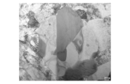
また、2相粒子の各相の結晶構造を確認するため、透過型電子顕微鏡(TEM:日立製作所製、HF-2000)を用いて粒子観察を実施し、EDX(エネルギー分散型X線分光法)分析及び電子線回折分析を実施した。本発明例4の観察結果を図3に示す。
電子線回折の結果、2相粒子が、主成分をCu5Zr(空間群F-43m(216))またはCu51Zr14(空間群P6/m(175))とする金属間化合物の相と、主成分をCu5Ca(空間群P6/mmm(191))とする金属間化合物の相と、で構成されていることを確認した。
電子線回折の結果、2相粒子が、主成分をCu5Zr(空間群F-43m(216))またはCu51Zr14(空間群P6/m(175))とする金属間化合物の相と、主成分をCu5Ca(空間群P6/mmm(191))とする金属間化合物の相と、で構成されていることを確認した。
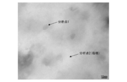
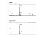
さらに、単相粒子の生成状態を確認するため、TEMおよびEDX分析装置(Kevex製、EDX分析装置Sigma)を用いて粒子観察を実施した。750,000倍(観察視野面積は約2×10⁴nm2)で1nm以上50nm以下の粒径の単相粒子の観察を実施した。さらに、EDX(エネルギー分散型X線分光法)分析により、単相粒子の組成を分析した。本発明例4の観察結果を図4A及び図4Bに示す。
EDX分析の結果から、Cuの母相中に分散析出された単相粒子は、CuとZrによる粒子であることを確認した。
なお、図4A及び図4Bでの分析点1がCuとZrが主成分である1相により構成される単相粒子である。一方、分析点2は、本発明例4の電子・電気機器銅合金の母相を分析している。
EDX分析の結果から、Cuの母相中に分散析出された単相粒子は、CuとZrによる粒子であることを確認した。
なお、図4A及び図4Bでの分析点1がCuとZrが主成分である1相により構成される単相粒子である。一方、分析点2は、本発明例4の電子・電気機器銅合金の母相を分析している。
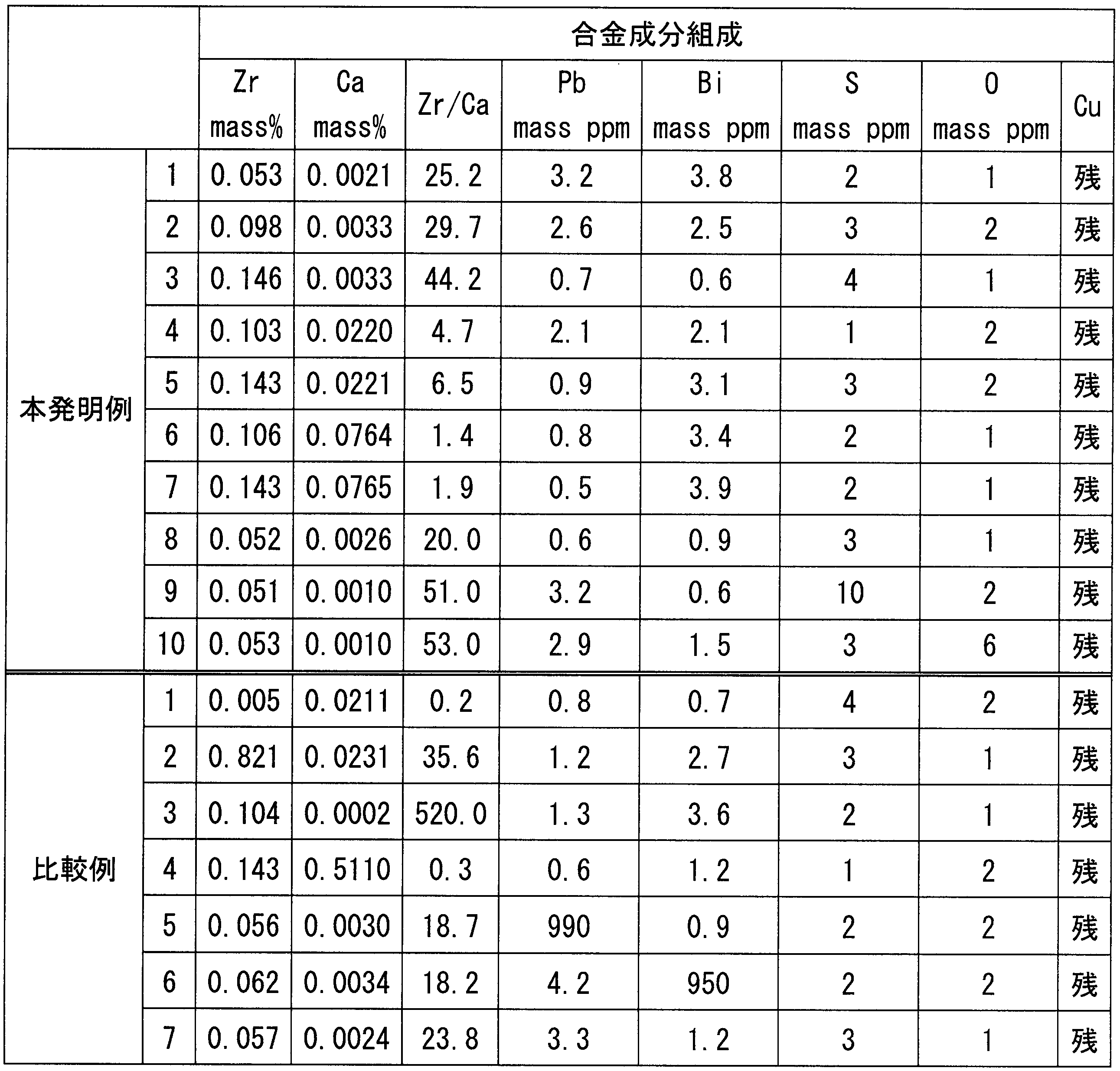
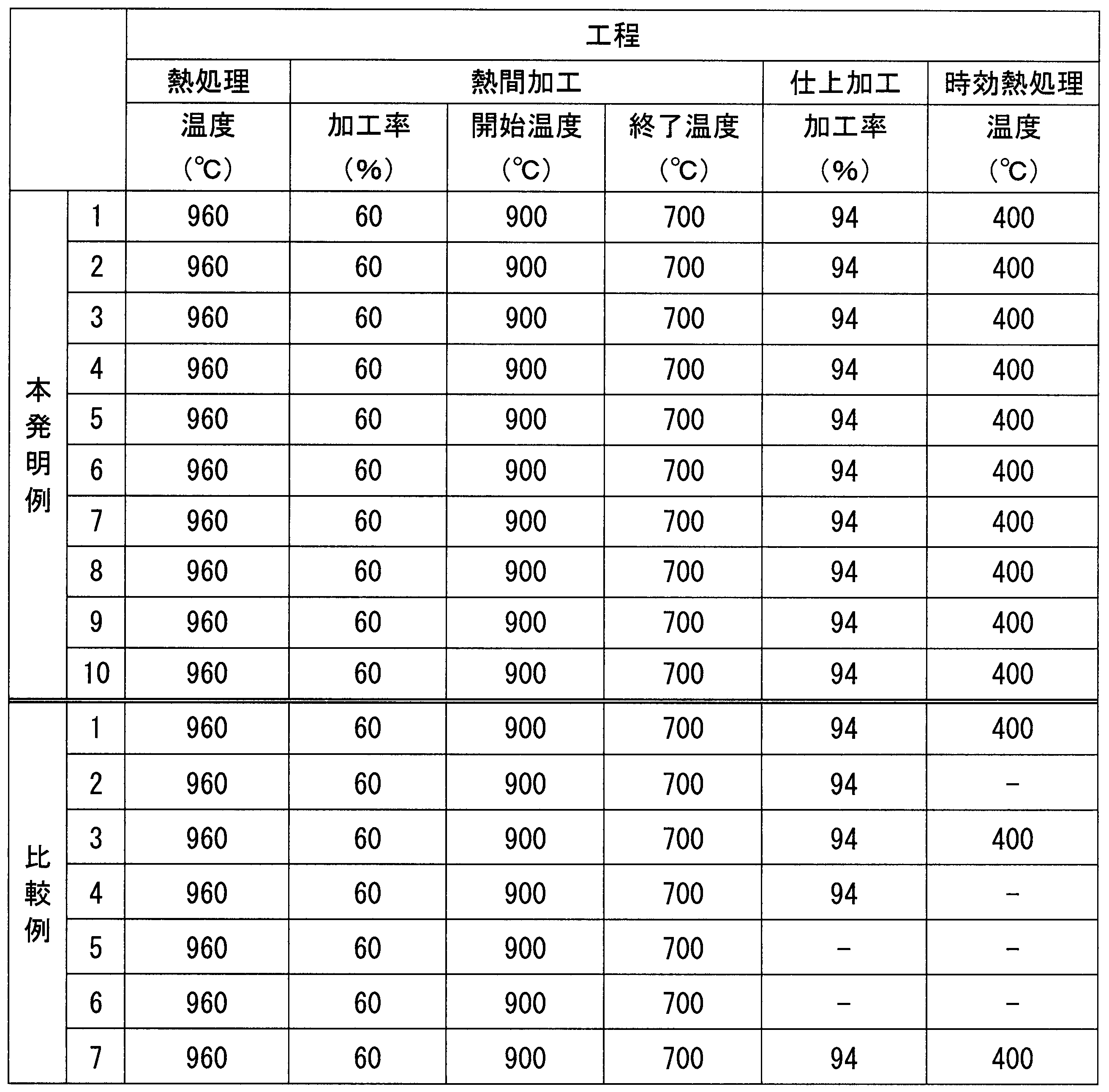

Zrの含有量が本発明の範囲よりも低い比較例1においては、粒径0.1μm以上の2相粒子がほとんど存在しておらず、破断面割合が低く、かつ、かえり高さも高くなっており、せん断加工性に劣ることが確認された。また、強度も不十分であった。
Caの含有量が本発明の範囲よりも低い比較例3においては、粒径0.1μm以上の2相粒子がほとんど存在しておらず、破断面割合が低く、かつ、かえり高さも高くなっており、せん断加工性に劣ることが確認された。
また、Zr、Caの含有量が本発明の範囲よりも高い比較例2、4においては、冷間圧延時に大きな耳割れが発生したため、加工が困難となったため作製を中止した。冷間加工性に劣ることが確認された。
Caの含有量が本発明の範囲よりも低い比較例3においては、粒径0.1μm以上の2相粒子がほとんど存在しておらず、破断面割合が低く、かつ、かえり高さも高くなっており、せん断加工性に劣ることが確認された。
また、Zr、Caの含有量が本発明の範囲よりも高い比較例2、4においては、冷間圧延時に大きな耳割れが発生したため、加工が困難となったため作製を中止した。冷間加工性に劣ることが確認された。
Pb、Biの含有量が本発明の範囲よりも高い比較例5,6においては、熱間加工中に割れが発生し、加工が困難となったため作製を中止した。
導電率が本発明の範囲よりも低い比較例7においては、強度が不十分であった。
導電率が本発明の範囲よりも低い比較例7においては、強度が不十分であった。
これに対して、本発明例1~10においては、熱間加工、冷間加工の際、いずれも3mm以上の大きな耳割れは発生しておらず、熱間加工性、冷間加工性が確保されている。また、いずれも粒径0.1μm以上の2相粒子が存在しており、破断面割合が高く、かつ、かえり高さも低くなっており、せん断加工性が向上していることが確認された。
以上のことから、CuとZrを主成分とする相とCuとCaを主成分とする相の2相により構成される2相粒子と、CuとZrが主成分である1相により構成される単相粒子と、を有する本発明例によれば、高強度、高導電性、優れたせん断加工性を有し、電子電気部品に適した電子機器用銅合金を提供することができることが確認された。
本発明の電子・電気機器用銅合金は、優れた導電率、強度、せん断加工性を有するので、寸法精度に優れ、且つ小型化及び薄肉化しても優れた特性を発揮する電子・電気機器用部品及び端子を提供できる。また、本発明の電子・電気機器用部品及び端子によれば、電子・電気機器を小型化、軽量化できる。
Claims (5)
- Zrの含有量が0.05mass%以上0.15mass%以下、Caの含有量が0.001mass%以上0.08mass%未満、Pbの含有量が0.05mass%未満、Biの含有量が0.01mass%未満とされ、残部がCuおよび不可避的不純物からなる組成を有し、
Zrの含有量(mass%)とCaの含有量(mass%)との比Zr/Caが1.2以上とされており、
CuとZrを主成分とする相とCuとCaを主成分とする相の2相により構成される2相粒子と、CuとZrが主成分である1相により構成される単相粒子と、を有するとともに、
導電率が88%IACSを超えていることを特徴とする電子・電気機器用銅合金。 - 請求項1に記載の電子・電気機器用銅合金において、
前記2相粒子は、Cu5ZrまたはCu51Zr14の結晶構造を有する金属間化合物からなる相と、Cu5Caの結晶構造を有する金属間化合物からなる相と、で構成されていることを特徴とする電子・電気機器用銅合金。 - 請求項1または請求項2に記載の電子・電気機器用銅合金において、
Sの含有量が0.0005mass%以下、Oの含有量が0.0003mass%以下とされていることを特徴とする電子・電気機器用銅合金。 - 請求項1から請求項3のいずれか一項に記載の電子機器用銅合金からなること特徴とする電子・電気機器用部品。
- 請求項1から請求項3のいずれか一項に記載の電子機器用銅合金からなること特徴とする端子。
Priority Applications (2)
| Application Number | Priority Date | Filing Date | Title |
|---|---|---|---|
| US14/653,568 US20150348664A1 (en) | 2013-01-09 | 2013-12-20 | Copper alloy for electronic and electric devices, component for electronic and electric devices, and terminal |
| CN201380062952.XA CN104822853A (zh) | 2013-01-09 | 2013-12-20 | 电子电气设备用铜合金、电子电气设备用零件及端子 |
Applications Claiming Priority (2)
| Application Number | Priority Date | Filing Date | Title |
|---|---|---|---|
| JP2013-001941 | 2013-01-09 | ||
| JP2013001941A JP5560475B2 (ja) | 2013-01-09 | 2013-01-09 | 電子・電気機器用銅合金、電子・電気機器用部品及び端子 |
Publications (1)
| Publication Number | Publication Date |
|---|---|
| WO2014109211A1 true WO2014109211A1 (ja) | 2014-07-17 |
Family
ID=51166869
Family Applications (1)
| Application Number | Title | Priority Date | Filing Date |
|---|---|---|---|
| PCT/JP2013/084251 Ceased WO2014109211A1 (ja) | 2013-01-09 | 2013-12-20 | 電子・電気機器用銅合金、電子・電気機器用部品及び端子 |
Country Status (5)
| Country | Link |
|---|---|
| US (1) | US20150348664A1 (ja) |
| JP (1) | JP5560475B2 (ja) |
| CN (1) | CN104822853A (ja) |
| TW (1) | TWI502084B (ja) |
| WO (1) | WO2014109211A1 (ja) |
Cited By (1)
| Publication number | Priority date | Publication date | Assignee | Title |
|---|---|---|---|---|
| CN108728686A (zh) * | 2017-04-13 | 2018-11-02 | 株式会社Sh铜业 | 铜合金材料、铜合金材料的制造方法和笼型转子 |
Families Citing this family (5)
| Publication number | Priority date | Publication date | Assignee | Title |
|---|---|---|---|---|
| JP6388437B2 (ja) * | 2014-09-19 | 2018-09-12 | 三菱マテリアル株式会社 | 電子・電気機器用銅合金、電子・電気機器用銅合金薄板、電子・電気機器用部品、端子及びバスバー |
| WO2017170699A1 (ja) | 2016-03-30 | 2017-10-05 | 三菱マテリアル株式会社 | 電子・電気機器用銅合金、電子・電気機器用銅合金板条材、電子・電気機器用部品、端子、バスバー、及び、リレー用可動片 |
| FI3438299T3 (fi) | 2016-03-30 | 2023-05-23 | Mitsubishi Materials Corp | Kupariseoksesta valmistettu nauha elektronisia laitteita ja sähkölaitteita varten, komponentti, liitosnapa, virtakisko sekä liikuteltava kappale releitä varten |
| JP6780187B2 (ja) | 2018-03-30 | 2020-11-04 | 三菱マテリアル株式会社 | 電子・電気機器用銅合金、電子・電気機器用銅合金板条材、電子・電気機器用部品、端子、及び、バスバー |
| CN111788320B (zh) * | 2018-03-30 | 2022-01-14 | 三菱综合材料株式会社 | 电子电气设备用铜合金﹑电子电气设备用铜合金板条材、电子电气设备用组件、端子及汇流排 |
Citations (3)
| Publication number | Priority date | Publication date | Assignee | Title |
|---|---|---|---|---|
| JPH10195562A (ja) * | 1997-01-09 | 1998-07-28 | Furukawa Electric Co Ltd:The | 打抜加工性に優れた電気電子機器用銅合金およびその製造方法 |
| JP2007126687A (ja) * | 2005-11-01 | 2007-05-24 | Nikko Kinzoku Kk | 銅合金箔 |
| JP2011058029A (ja) * | 2009-09-08 | 2011-03-24 | Mitsubishi Shindoh Co Ltd | 銅合金箔 |
Family Cites Families (4)
| Publication number | Priority date | Publication date | Assignee | Title |
|---|---|---|---|---|
| CN1177946C (zh) * | 2001-09-07 | 2004-12-01 | 同和矿业株式会社 | 连接器用铜合金及其制造方法 |
| JP3999676B2 (ja) * | 2003-01-22 | 2007-10-31 | Dowaホールディングス株式会社 | 銅基合金およびその製造方法 |
| JP4118832B2 (ja) * | 2004-04-14 | 2008-07-16 | 三菱伸銅株式会社 | 銅合金及びその製造方法 |
| KR101136265B1 (ko) * | 2006-07-21 | 2012-04-23 | 가부시키가이샤 고베 세이코쇼 | 전기 전자 부품용 구리 합금판 |
-
2013
- 2013-01-09 JP JP2013001941A patent/JP5560475B2/ja not_active Expired - Fee Related
- 2013-12-20 CN CN201380062952.XA patent/CN104822853A/zh active Pending
- 2013-12-20 US US14/653,568 patent/US20150348664A1/en not_active Abandoned
- 2013-12-20 WO PCT/JP2013/084251 patent/WO2014109211A1/ja not_active Ceased
- 2013-12-25 TW TW102148188A patent/TWI502084B/zh not_active IP Right Cessation
Patent Citations (3)
| Publication number | Priority date | Publication date | Assignee | Title |
|---|---|---|---|---|
| JPH10195562A (ja) * | 1997-01-09 | 1998-07-28 | Furukawa Electric Co Ltd:The | 打抜加工性に優れた電気電子機器用銅合金およびその製造方法 |
| JP2007126687A (ja) * | 2005-11-01 | 2007-05-24 | Nikko Kinzoku Kk | 銅合金箔 |
| JP2011058029A (ja) * | 2009-09-08 | 2011-03-24 | Mitsubishi Shindoh Co Ltd | 銅合金箔 |
Cited By (2)
| Publication number | Priority date | Publication date | Assignee | Title |
|---|---|---|---|---|
| CN108728686A (zh) * | 2017-04-13 | 2018-11-02 | 株式会社Sh铜业 | 铜合金材料、铜合金材料的制造方法和笼型转子 |
| CN108728686B (zh) * | 2017-04-13 | 2021-05-04 | 株式会社日立金属新材料 | 铜合金材料、铜合金材料的制造方法和笼型转子 |
Also Published As
| Publication number | Publication date |
|---|---|
| TW201439341A (zh) | 2014-10-16 |
| US20150348664A1 (en) | 2015-12-03 |
| JP5560475B2 (ja) | 2014-07-30 |
| JP2014133913A (ja) | 2014-07-24 |
| CN104822853A (zh) | 2015-08-05 |
| TWI502084B (zh) | 2015-10-01 |
Similar Documents
| Publication | Publication Date | Title |
|---|---|---|
| JP5668814B1 (ja) | 電子・電気機器用銅合金、電子・電気機器用銅合金薄板、電子・電気機器用部品、端子およびバスバー | |
| JP5045784B2 (ja) | 電子機器用銅合金、電子機器用銅合金の製造方法及び電子機器用銅合金圧延材 | |
| JP5712585B2 (ja) | 電子機器用銅合金、電子機器用銅合金の製造方法及び電子機器用銅合金圧延材 | |
| US10453582B2 (en) | Copper alloy for electronic/electrical device, copper alloy plastically-worked material for electronic/electrical device, component for electronic/electrical device, terminal, and busbar | |
| JP6464742B2 (ja) | 電子・電気機器用銅合金、電子・電気機器用銅合金薄板、電子・電気機器用部品、端子及びバスバー | |
| TW201738394A (zh) | 電子‧電氣機器用銅合金、電子‧電氣機器用銅合金板條材、電子‧電氣機器用零件、端子、匯流條、及中繼用可動片 | |
| WO2020122230A1 (ja) | 純銅板、電子・電気機器用部材、放熱用部材 | |
| JP5560475B2 (ja) | 電子・電気機器用銅合金、電子・電気機器用部品及び端子 | |
| WO2017170699A1 (ja) | 電子・電気機器用銅合金、電子・電気機器用銅合金板条材、電子・電気機器用部品、端子、バスバー、及び、リレー用可動片 | |
| WO2015087624A1 (ja) | 電子・電気機器用銅合金、電子・電気機器用銅合金塑性加工材、電子・電気機器用部品及び端子 | |
| JP6311299B2 (ja) | 電子・電気機器用銅合金、電子・電気機器用銅合金塑性加工材、電子・電気機器用銅合金塑性加工材の製造方法、電子・電気機器用部品及び端子 | |
| JP6388437B2 (ja) | 電子・電気機器用銅合金、電子・電気機器用銅合金薄板、電子・電気機器用部品、端子及びバスバー | |
| JP6248389B2 (ja) | 電子・電気機器用銅合金、電子・電気機器用部品及び端子 | |
| JP2015034332A (ja) | 電子・電気機器用銅合金、電子・電気機器用銅合金薄板、電子・電気機器用導電部品及び端子 | |
| JP5748945B2 (ja) | 銅合金材の製造方法とそれにより得られる銅合金材 | |
| JP6464740B2 (ja) | 電子・電気機器用銅合金、電子・電気機器用銅合金薄板、電子・電気機器用部品、端子及びバスバー | |
| JP2016216794A (ja) | 銅合金板および銅合金板の製造方法 | |
| JP6248386B2 (ja) | 電子・電気機器用銅合金、電子・電気機器用部品及び端子 | |
| JP2013104096A (ja) | 電子機器用銅合金、電子機器用銅合金の製造方法、電子機器用銅合金塑性加工材および電子機器用部品 | |
| JP6464741B2 (ja) | 電子・電気機器用銅合金、電子・電気機器用銅合金薄板、電子・電気機器用部品、端子及びバスバー | |
| JP2015014040A (ja) | Ti含有銅合金の製造方法 |
Legal Events
| Date | Code | Title | Description |
|---|---|---|---|
| 121 | Ep: the epo has been informed by wipo that ep was designated in this application |
Ref document number: 13871279 Country of ref document: EP Kind code of ref document: A1 |
|
| WWE | Wipo information: entry into national phase |
Ref document number: 14653568 Country of ref document: US |
|
| NENP | Non-entry into the national phase |
Ref country code: DE |
|
| 122 | Ep: pct application non-entry in european phase |
Ref document number: 13871279 Country of ref document: EP Kind code of ref document: A1 |