WO2014109196A1 - プローブ装置及びウエハ搬送システム - Google Patents
プローブ装置及びウエハ搬送システム Download PDFInfo
- Publication number
- WO2014109196A1 WO2014109196A1 PCT/JP2013/084000 JP2013084000W WO2014109196A1 WO 2014109196 A1 WO2014109196 A1 WO 2014109196A1 JP 2013084000 W JP2013084000 W JP 2013084000W WO 2014109196 A1 WO2014109196 A1 WO 2014109196A1
- Authority
- WO
- WIPO (PCT)
- Prior art keywords
- semiconductor wafer
- wafer
- gas ejection
- nozzle
- gas
- Prior art date
- Legal status (The legal status is an assumption and is not a legal conclusion. Google has not performed a legal analysis and makes no representation as to the accuracy of the status listed.)
- Ceased
Links
Images


Classifications
-
- G—PHYSICS
- G01—MEASURING; TESTING
- G01R—MEASURING ELECTRIC VARIABLES; MEASURING MAGNETIC VARIABLES
- G01R31/00—Arrangements for testing electric properties; Arrangements for locating electric faults; Arrangements for electrical testing characterised by what is being tested not provided for elsewhere
- G01R31/26—Testing of individual semiconductor devices
- G01R31/2601—Apparatus or methods therefor
-
- H—ELECTRICITY
- H10—SEMICONDUCTOR DEVICES; ELECTRIC SOLID-STATE DEVICES NOT OTHERWISE PROVIDED FOR
- H10P—GENERIC PROCESSES OR APPARATUS FOR THE MANUFACTURE OR TREATMENT OF DEVICES COVERED BY CLASS H10
- H10P72/00—Handling or holding of wafers, substrates or devices during manufacture or treatment thereof
- H10P72/70—Handling or holding of wafers, substrates or devices during manufacture or treatment thereof for supporting or gripping
- H10P72/78—Handling or holding of wafers, substrates or devices during manufacture or treatment thereof for supporting or gripping using vacuum or suction, e.g. Bernoulli chucks
-
- G—PHYSICS
- G01—MEASURING; TESTING
- G01R—MEASURING ELECTRIC VARIABLES; MEASURING MAGNETIC VARIABLES
- G01R1/00—Details of instruments or arrangements of the types included in groups G01R5/00 - G01R13/00 and G01R31/00
- G01R1/02—General constructional details
- G01R1/06—Measuring leads; Measuring probes
- G01R1/067—Measuring probes
-
- G—PHYSICS
- G01—MEASURING; TESTING
- G01R—MEASURING ELECTRIC VARIABLES; MEASURING MAGNETIC VARIABLES
- G01R31/00—Arrangements for testing electric properties; Arrangements for locating electric faults; Arrangements for electrical testing characterised by what is being tested not provided for elsewhere
- G01R31/28—Testing of electronic circuits, e.g. by signal tracer
- G01R31/282—Testing of electronic circuits specially adapted for particular applications not provided for elsewhere
- G01R31/2831—Testing of materials or semi-finished products, e.g. semiconductor wafers or substrates
-
- G—PHYSICS
- G01—MEASURING; TESTING
- G01R—MEASURING ELECTRIC VARIABLES; MEASURING MAGNETIC VARIABLES
- G01R31/00—Arrangements for testing electric properties; Arrangements for locating electric faults; Arrangements for electrical testing characterised by what is being tested not provided for elsewhere
- G01R31/28—Testing of electronic circuits, e.g. by signal tracer
- G01R31/2851—Testing of integrated circuits [IC]
- G01R31/2855—Environmental, reliability or burn-in testing
- G01R31/286—External aspects, e.g. related to chambers, contacting devices or handlers
- G01R31/2865—Holding devices, e.g. chucks; Handlers or transport devices
- G01R31/2867—Handlers or transport devices, e.g. loaders, carriers, trays
-
- G—PHYSICS
- G03—PHOTOGRAPHY; CINEMATOGRAPHY; ANALOGOUS TECHNIQUES USING WAVES OTHER THAN OPTICAL WAVES; ELECTROGRAPHY; HOLOGRAPHY
- G03F—PHOTOMECHANICAL PRODUCTION OF TEXTURED OR PATTERNED SURFACES, e.g. FOR PRINTING, FOR PROCESSING OF SEMICONDUCTOR DEVICES; MATERIALS THEREFOR; ORIGINALS THEREFOR; APPARATUS SPECIALLY ADAPTED THEREFOR
- G03F7/00—Photomechanical, e.g. photolithographic, production of textured or patterned surfaces, e.g. printing surfaces; Materials therefor, e.g. comprising photoresists; Apparatus specially adapted therefor
- G03F7/70—Microphotolithographic exposure; Apparatus therefor
- G03F7/708—Construction of apparatus, e.g. environment aspects, hygiene aspects or materials
- G03F7/70858—Environment aspects, e.g. pressure of beam-path gas, temperature
- G03F7/70866—Environment aspects, e.g. pressure of beam-path gas, temperature of mask or workpiece
-
- H—ELECTRICITY
- H10—SEMICONDUCTOR DEVICES; ELECTRIC SOLID-STATE DEVICES NOT OTHERWISE PROVIDED FOR
- H10P—GENERIC PROCESSES OR APPARATUS FOR THE MANUFACTURE OR TREATMENT OF DEVICES COVERED BY CLASS H10
- H10P72/00—Handling or holding of wafers, substrates or devices during manufacture or treatment thereof
- H10P72/70—Handling or holding of wafers, substrates or devices during manufacture or treatment thereof for supporting or gripping
- H10P72/76—Handling or holding of wafers, substrates or devices during manufacture or treatment thereof for supporting or gripping using mechanical means, e.g. clamps or pinches
- H10P72/7602—Handling or holding of wafers, substrates or devices during manufacture or treatment thereof for supporting or gripping using mechanical means, e.g. clamps or pinches the wafers being placed on a robot blade or gripped by a gripper for conveyance
Definitions
- the present invention relates to a probe apparatus and a wafer transfer system.
- a probe device is used for performing an electrical inspection of a semiconductor device formed on a semiconductor wafer.
- a measurement unit that performs electrical measurement by bringing a probe into contact with an electrode of a semiconductor device formed on a semiconductor wafer on a mounting table, and a wafer carrier (wafer cassette or FOUP) are mounted.
- a load port and a transfer unit including a transfer mechanism for transferring a semiconductor wafer between a wafer carrier and a mounting table are included in the configuration, and a transfer mechanism including a wafer transfer arm is known (for example, Patent Documents). 1).
- a semiconductor wafer is conveyed by vacuum suction onto a wafer transfer arm.
- An object of the present invention is to provide a probe device and a wafer transfer system that can suppress the occurrence of a transfer error and the like by sucking and holding the semiconductor wafer even when the semiconductor wafer is warped.
- a probe apparatus that performs electrical measurement of a semiconductor device formed on a semiconductor wafer on a mounting table, and is mounted on the mounting table.
- a measurement unit that performs electrical measurement by bringing a probe into contact with the semiconductor device of the semiconductor wafer; a load port on which a wafer carrier that accommodates the semiconductor wafer is placed; and a suction unit that vacuum-sucks the semiconductor wafer
- a wafer transfer mechanism for transferring the semiconductor wafer between the wafer carrier and the mounting table, and an upper surface of the semiconductor wafer when the semiconductor wafer accommodated in the wafer carrier is vacuum-sucked to the suction portion
- a probe device having a gas jetting mechanism for blowing a gas onto the probe.
- the gas ejection mechanism is configured to blow a gas to a central portion of the semiconductor wafer.
- the gas ejection mechanism includes a nozzle that ejects the gas, and a base end portion of the nozzle includes a standby position where the entire nozzle does not exist above the semiconductor wafer and a tip end portion of the nozzle. It is preferable to be fixed to a rotation drive mechanism for rotating the nozzle between a gas ejection position located above the semiconductor wafer.
- the wafer carrier and the mounting table described above include a load port on which a wafer carrier that accommodates a semiconductor wafer is placed, and a suction portion that vacuum-sucks the semiconductor wafer.
- a wafer transfer system is provided.
- the gas ejection mechanism is configured to blow a gas to a central portion of the semiconductor wafer.
- the gas ejection mechanism includes a nozzle that ejects the gas, and a base end portion of the nozzle includes a standby position where the entire nozzle does not exist above the semiconductor wafer and a tip end portion of the nozzle. It is preferable to be fixed to a rotation drive mechanism for rotating the nozzle between a gas ejection position located above the semiconductor wafer.
- the semiconductor wafer can be sucked and held, and the occurrence of a transport error or the like can be suppressed.
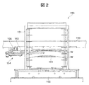
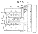
- FIG. 3 is a diagram used to explain a standby position where the entire gas ejection nozzle in FIG. 2 does not exist above the semiconductor wafer. It is a figure used for demonstrating the gas ejection position in which the front-end
- FIG. 1 is a plan view schematically showing a configuration of a probe apparatus according to an embodiment of the present invention.
- the measurement unit 110 includes a mounting table 111 on which the semiconductor wafer W can be moved, and can be moved back and forth, left and right, or up and down.
- a plurality of probes and semiconductor wafers W are provided on a probe card (not shown) by driving the mounting table 111.
- the electrical characteristics of the semiconductor device are measured by contact with the electrodes of the formed semiconductor device.
- the loader unit 150 includes a load port 152 on which a wafer cassette 151 serving as a wafer carrier for accommodating the semiconductor wafer W is placed on the front side (lower side in FIG. 1), and the wafer is transferred so as to be adjacent to the load port 152.
- a mechanism 160 is provided.
- the loader unit 150 includes an alignment mechanism 170 on the rear side (upper side in FIG. 1). The alignment mechanism 170 rotates the semiconductor wafer W to detect the position of the notch of the semiconductor wafer W and the eccentricity state of the semiconductor wafer W.
- the wafer transfer mechanism 160 includes a wafer transfer arm 161 for transferring the semiconductor wafer W by vacuum suction, and the wafer transfer arm 161 includes a plurality of suction portions (suction pads) 162 for vacuum suction of the semiconductor wafer W (this embodiment). 2) in the form of.
- a vacuum line (not shown in FIG. 1) connected to a suction source such as a vacuum pump is connected to the suction unit 162. Note that a plurality of wafer transfer arms 161 may be provided one above the other as needed.
- the wafer transfer mechanism 160 is arranged between the wafer cassette 151 placed on the load port 152, the alignment mechanism 170, and the placement table 111 of the measurement unit 110 by moving and turning the wafer transfer arm 161 back and forth, left and right, or up and down. Then, the semiconductor wafer W is transferred.
- the load port 152 freely moves up and down by a not-shown up-and-down moving mechanism, and the support frame 153 is provided between the load port 152 and the wafer transfer mechanism 160 and includes an optical detector (not shown).
- the optical detector detects the presence / absence of the semiconductor wafer W while moving the wafer cassette 151 mounted on the load port 152 up and down by moving the load port 152 up and down, and the wafer on which the semiconductor wafer W is disposed. A slot in the cassette 151 is detected.
- the support frame 153 includes a gas ejection mechanism 154.
- the gas ejection mechanism 154 includes a gas ejection nozzle 155 formed from a pipe-shaped member (FIGS. 2, 3A, and 3B).
- the base end portion of the gas ejection nozzle 155 is fixed to the following rotation drive mechanism 156 provided in the support frame 153.
- the rotation drive mechanism 156 is configured so that the gas ejection nozzle 155 does not exist entirely above the semiconductor wafer W, and the gas ejection nozzle 155 has a gas ejection nozzle in which the tip of the gas ejection nozzle 155 is located above the center of the semiconductor wafer W
- the gas ejection nozzle 155 can be swung around the base end of the gas ejection nozzle 155 fixed to the rotational drive mechanism 156 between the position (FIG. 3B).
- the wafer cassette 151 is configured to accommodate a warped semiconductor wafer W, and has a wider slot interval than a normal wafer cassette. It is set to about 6 times (slot pitch is about 23 mm to 29 mm, for example). The number of slots is smaller than that of a normal wafer cassette, and is, for example, about 6 to 8.
- the wafer transfer arm 161 of the transfer mechanism 160 When the semiconductor wafer W having warpage in the wafer cassette 151 is attracted and held by the wafer transfer arm 161 of the transfer mechanism 160, as shown in FIGS.
- the warp of the semiconductor wafer W is reduced by ejecting gas (air in the present embodiment) downward by the gas ejection nozzle 155 and pressing the central portion of the semiconductor wafer W downward with the gas pressure.
- the wafer transfer arm 161 adsorbs the semiconductor wafer W.
- the wafer transfer arm 161 when the semiconductor wafer W warped so that the central portion is convex upward is attracted and held by the wafer transfer arm 161 from the lower side of the semiconductor wafer W, the wafer is An interval is generated between the suction portion 162 of the transfer arm 161 and the back surface of the semiconductor wafer W, making it difficult to vacuum-suck the semiconductor wafer W. Therefore, in the present embodiment, the gas ejection nozzle 155 ejects a gas from the substantially central portion on the upper side of the semiconductor wafer W to the lower side, and the wafer transfer arm 161 causes the central portion of the semiconductor wafer W to flow at the gas pressure. The pressed semiconductor wafer W is vacuum-sucked. Thereby, the wafer transfer arm 161 can vacuum-suck the semiconductor wafer W in a state where the warp of the semiconductor wafer W is substantially reduced, and can hold the semiconductor wafer W having warp with higher probability.
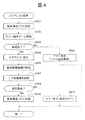
- FIG. 4 is a flowchart showing a procedure of air assist processing for ejecting gas from the gas ejection nozzle 155 in FIG. 3B toward the semiconductor wafer W.
- the rotation drive mechanism 156 turns the gas ejection nozzle 155 located at the standby position (FIG. 3A) to position the tip of the gas ejection nozzle 155 at the gas ejection position above the center of the semiconductor wafer W.
- the wafer transfer mechanism 160 drives the wafer transfer arm 161 to insert it under the semiconductor wafer W (Step S402).
- the gas ejection mechanism 154 determines whether or not the rotation of the gas ejection nozzle 155 is completed (step S403), and when the rotation of the gas ejection nozzle 155 is completed as a result of the determination in step S403 (in step S403). Yes) ejects gas from the gas ejection nozzle 155 toward the semiconductor wafer W (hereinafter referred to as “air assist”) (step S404).
- Step S403 when the turning of the gas ejection nozzle 155 is not completed (No in step S403), an error display of “nozzle turning abnormality” is displayed, for example, a display device (not shown) connected to the outside of the probe device 100. (Step S405), and the process is terminated.
- step S406 a vacuum suction mechanism including a suction source such as a vacuum pump connected to a suction unit 162 provided in the wafer transfer arm 161 via a vacuum line (not shown) is driven. Subsequently, the vertical movement mechanism of the load port 152 is driven to lower the wafer cassette 151 (step S407), and the wafer transfer arm 161 vacuum-sucks the semiconductor wafer W.
- a vacuum suction mechanism including a suction source such as a vacuum pump connected to a suction unit 162 provided in the wafer transfer arm 161 via a vacuum line (not shown) is driven.
- the vertical movement mechanism of the load port 152 is driven to lower the wafer cassette 151 (step S407), and the wafer transfer arm 161 vacuum-sucks the semiconductor wafer W.
- the rotation drive mechanism 156 determines whether or not the semiconductor wafer W is vacuum-sucked to the wafer transfer arm 161 (step S408). If the result of determination in step S408 is vacuum-suck (Yes in step S408). ) Swivels the gas ejection nozzle 155 to return it to the standby position (step S409), and ends this process.
- the moving mechanism is driven to move the wafer cassette 151 up and down, and the optical detector detects a slot in the wafer cassette 151 in which the semiconductor wafer W is accommodated.
- the wafer transfer arm 161 vacuum-sucks the semiconductor wafer W whose warpage has been reduced by performing air assist using the gas ejection nozzle 155 of the gas ejection mechanism 154 and transports it to the alignment mechanism 170.
- the alignment mechanism 170 detects the position of the semiconductor wafer W by detecting the notch of the semiconductor wafer W.
- the wafer transfer arm 161 takes out the semiconductor wafer W whose position is detected by the alignment mechanism 170 from the alignment mechanism 170 and places it on the mounting table 111 of the measurement unit 110.
- the electrical characteristics of the semiconductor wafer W on the mounting table 111 are inspected by bringing the probe of the probe card into contact with the semiconductor device of the semiconductor wafer W. Specifically, the inspection of the electrical characteristics of the semiconductor device is performed by supplying a test signal from a tester (not shown) to the semiconductor device and measuring an output signal output from the semiconductor device to the tester.
- the wafer transfer arm 161 accommodates the semiconductor wafer W on the mounting table 111 in the wafer cassette 151.
- step S404 since air assist is performed to eject gas toward the warped semiconductor wafer W (step S404), the wafer transfer arm 161 sucks and holds the semiconductor wafer W with reduced warpage. Therefore, the occurrence of a transport error can be suppressed.
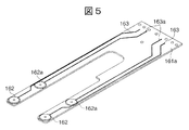
- the wafer transfer arm 161a having a configuration shown in FIG. That is, the wafer transfer arm 161a shown in FIG. 5 includes two suction portions 162a on the rear end side in the longitudinal direction in addition to the two suction portions 162 of the transfer arm 161 shown in FIG. 1, FIG. 3A, FIG. And has a total of four suction portions 162, 162a. Further, a vacuum line 163 is connected to the suction part 162 and a vacuum line 163a is connected to the suction part 162a, and the vacuum suction of the suction part 162 and the suction part 162a can be performed independently.
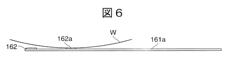
- the wafer transfer arm 161a having the above-described configuration is used, for example, as shown in FIG. 6, when the semiconductor wafer W whose center part is warped concavely toward the lower side is vacuum-sucked, only the tip-side suction part 162 is used. Even when vacuum suction cannot be performed, the wafer transfer arm 161a may be able to suck and hold the semiconductor wafer W by vacuum suction of the suction portion 162a on the rear end side. In addition, as the semiconductor wafer W is vacuum-sucked by the suction part 162a on the rear end side, the semiconductor wafer W may be vacuum-sucked by the suction part 162 on the front end side.
- the semiconductor wafer W is vacuum-sucked using both the part 162a and the tip-side suction part 162.
- the vacuum suction mechanism including the suction part that is vacuum-sucked can be driven. it can.
- the measurement unit of the probe device 100 described above may be configured by connecting an external device, and the present invention is configured by the external device and a device that implements the functions of the above-described embodiments. It may be a wafer transfer system.
- Probe apparatus 110 Measuring part 111 Mounting stand 150 Loader part 151 Wafer cassette 152 Load port 153 Support frame 154 Gas ejection mechanism 155 Gas ejection nozzle 156 Rotation drive mechanism 160 Wafer conveyance mechanism 161 Wafer conveyance arm 162 Adsorption part 170 Positioning mechanism
Landscapes
- Engineering & Computer Science (AREA)
- Physics & Mathematics (AREA)
- General Physics & Mathematics (AREA)
- General Engineering & Computer Science (AREA)
- Environmental & Geological Engineering (AREA)
- Health & Medical Sciences (AREA)
- Microelectronics & Electronic Packaging (AREA)
- Computer Hardware Design (AREA)
- Life Sciences & Earth Sciences (AREA)
- Atmospheric Sciences (AREA)
- Toxicology (AREA)
- Epidemiology (AREA)
- Public Health (AREA)
- Container, Conveyance, Adherence, Positioning, Of Wafer (AREA)
- Testing Or Measuring Of Semiconductors Or The Like (AREA)
- Robotics (AREA)
Abstract
半導体ウエハが反っている場合でも半導体ウエハを吸着保持することにより、搬送エラー等の発生を抑制することのできるプローブ装置を提供する。プローブ装置100は、測定部110と、搬送ユニットであるローダー部150とを備える。ローダー部150は、ロードポート152に載置されるウエハカセット151、ウエハ搬送アーム161を有するウエハ搬送機構160、気体噴出ノズル155を有する気体噴出機構154を備える。ウエハ搬送アーム161がウエハカセット151内の反りのある半導体ウエハWを吸着保持するとき、気体噴出ノズル155が、半導体ウエハWの上側の略中央部から下側に向けて気体を噴出することによって半導体ウエハWの反りを減少させる。
Description
本発明はプローブ装置及びウエハ搬送システムに関する。
半導体デバイスの製造工程では、プローブ装置が半導体ウエハに形成された半導体デバイスの電気的な検査を行うために用いられている。このようなプローブ装置としては、載置台上の半導体ウエハに形成された半導体デバイスの電極にプローブを接触させて電気的な測定を行う測定部と、ウエハキャリア(ウエハカセット又はFOUP)を載置するロードポートと、ウエハキャリア及び載置台の間で半導体ウエハを搬送する搬送機構を備える搬送ユニットとを構成に有し、搬送機構としてはウエハ搬送アームを備えるものが知られている(例えば、特許文献1参照)。また、従来のプローブ装置において、半導体ウエハをウエハ搬送アームに真空吸着して搬送している。
しかしながら、半導体ウエハが反っている場合、半導体ウエハを真空吸着できずに搬送エラーとなってプローブ装置が停止してしまうという問題があった。このような半導体ウエハが反ることによってプローブ装置が停止する問題は、例えば、パワー半導体の需要が増加するにつれて進む半導体ウエハの薄化によって深刻化することが予想される。
本発明の目的は、半導体ウエハが反っている場合でも半導体ウエハを吸着保持することにより、搬送エラー等の発生を抑制することのできるプローブ装置及びウエハ搬送システムを提供することにある。
上記課題を解決するために、本発明によれば、半導体ウエハに形成された半導体デバイスの電気的な測定を載置台の上で行うプローブ装置であって、前記載置台の上に載置された前記半導体ウエハの前記半導体デバイスにプローブを接触させて電気的な測定を行う測定部と、前記半導体ウエハを収容するウエハキャリアが載置されるロードポートと、前記半導体ウエハを真空吸着する吸着部を有し、前記ウエハキャリアと前記載置台との間で前記半導体ウエハを搬送するウエハ搬送機構と、前記ウエハキャリアが収容する前記半導体ウエハを前記吸着部に真空吸着するときに、前記半導体ウエハの上面に気体を吹き付ける気体噴出機構とを有するプローブ装置が提供される。
本発明において、前記気体噴出機構は、前記半導体ウエハの中央部に気体を吹き付けるよう構成されていることが好ましい。
本発明において、前記気体噴出機構は、前記気体を噴出するノズルを備え、前記ノズルの基端部は、前記ノズルの全体が前記半導体ウエハの上方に存在しない待機位置と前記ノズルの先端部が前記半導体ウエハの上方に位置する気体噴出位置との間で前記ノズルを旋回させる回転駆動機構に固定されていることが好ましい。
上記課題を解決するために、本発明によれば、半導体ウエハを収容するウエハキャリアが載置されるロードポートと、前記半導体ウエハを真空吸着する吸着部を有し、前記ウエハキャリアと前記載置台との間で前記半導体ウエハを搬送するウエハ搬送機構と、前記ウエハキャリアが収容する前記半導体ウエハを前記吸着部に真空吸着するときに、前記半導体ウエハの上面に気体を吹き付ける気体噴出機構とを有するウエハ搬送システムが提供される。
本発明において、前記気体噴出機構は、前記半導体ウエハの中央部に気体を吹き付けるよう構成されていることが好ましい。
本発明において、前記気体噴出機構は、前記気体を噴出するノズルを備え、前記ノズルの基端部は、前記ノズルの全体が前記半導体ウエハの上方に存在しない待機位置と前記ノズルの先端部が前記半導体ウエハの上方に位置する気体噴出位置との間で前記ノズルを旋回させる回転駆動機構に固定されていることが好ましい。
本発明によれば、半導体ウエハが反っている場合でも半導体ウエハを吸着保持することができ、もって、搬送エラー等の発生を抑制することができる。
以下、本発明の実施の形態について図面を参照しながら説明する。
図1は、本発明の実施の形態に係るプローブ装置の構成を概略的に示す平面図である。
図1のプローブ装置100は、測定部110と、搬送ユニットであるローダー部150とを備える。測定部110は、前後、左右、又は上下に移動できると共に半導体ウエハWが載置される載置台111を備え、載置台111の駆動によって図示しないプローブカードに備えられたプローブと半導体ウエハWに複数形成された半導体デバイスの電極とが接触して半導体デバイスの電気的特性を測定する。
ローダー部150は、その前方側(図1において下側)に半導体ウエハWを収容するウエハキャリアとしてのウエハカセット151を載置するロードポート152を備え、且つロードポート152に隣接するようにウエハ搬送機構160を備える。また、ローダー部150は、その後方側(図1において上側)に位置合わせ機構170を備える。位置合わせ機構170は、半導体ウエハWを回転させて半導体ウエハWのノッチの位置と半導体ウエハWの偏芯の状態を検出する。
ウエハ搬送機構160は半導体ウエハWを真空吸着して搬送するためのウエハ搬送アーム161を備え、ウエハ搬送アーム161は半導体ウエハWを真空吸着するための吸着部(吸着パッド)162を複数(本実施の形態では2つ)備える。吸着部162には、真空ポンプ等の吸引源に接続された真空ライン(図1には図示せず。)が接続されている。なお、ウエハ搬送アーム161は必要に応じて上下に重ねて複数備えてもよい。
ウエハ搬送機構160は、ウエハ搬送アーム161の前後、左右、又は上下への移動及び旋回によってロードポート152に載置されたウエハカセット151、位置合わせ機構170、及び測定部110の載置台111の間で半導体ウエハWを搬送する。
ロードポート152は、不図示の上下動機構によって自在に上下動し、支持フレーム153は、ロードポート152とウエハ搬送機構160との間に備えられると共に図示しない光学検出器を備える。そして、光学検出器は、ロードポート152に載置されたウエハカセット151をロードポート152を上下動することによって上下動させながら半導体ウエハWの有無を検出すると共に、半導体ウエハWが配置されたウエハカセット151内のスロットを検出する。
また、上記支持フレーム153は、気体噴出機構154を備えている。気体噴出機構154は、パイプ状の部材から形成された気体噴出ノズル155を備えている(図2、図3A、及び図3B)。気体噴出ノズル155の基端部は、支持フレーム153に備えられた下記の回転駆動機構156に固定されている。そして、回転駆動機構156は、気体噴出ノズル155の全体が半導体ウエハWの上方に存在しない待機位置(図3A)と気体噴出ノズル155の先端部が半導体ウエハWの中央部上方に位置する気体噴出位置(図3B)との間で、回転駆動機構156に固定されている気体噴出ノズル155の基端部を軸に気体噴出ノズル155を旋回することができる。
本実施の形態において、ウエハカセット151は、図2に示すように、反りのある半導体ウエハWを収容可能な構成となっており、通常のウエハカセットに比べてスロットの間隔が広く、例えば、5~6倍程度(スロットピッチが例えば23mm~29mm程度)に設定されている。また、スロット数は通常のウエハカセットに比べて少なくなっており、例えば、6~8程度とされている。
ウエハカセット151内の反りのある半導体ウエハWを搬送機構160のウエハ搬送アーム161で吸着保持する際は、図2及び図3Bに示すように、半導体ウエハWの上側(上面)の略中央部から気体噴出ノズル155によって下側に向けて気体(本実施の形態では空気)を噴出して半導体ウエハWの中央部を気体の圧力で下方に向けて押圧することによって半導体ウエハWの反りを減少させてウエハ搬送アーム161で半導体ウエハWを吸着する。
具体的には、図2に示すように、中央部が上側に向けて凸状となるように反った半導体ウエハWを半導体ウエハWの下側からウエハ搬送アーム161によって吸着保持しようとすると、ウエハ搬送アーム161の吸着部162と半導体ウエハWの裏面との間に間隔が生じてしまい半導体ウエハWを真空吸着することが困難になる。したがって、本実施の形態では、気体噴出ノズル155が半導体ウエハWの上側の略中央部から下側に向けて気体を噴出して、ウエハ搬送アーム161が半導体ウエハWの中央部を気体の圧力で押圧されている状態の半導体ウエハWを真空吸着する。これにより、ウエハ搬送アーム161は、実質的に半導体ウエハWの反りが減少した状態で半導体ウエハWを真空吸着し、より高い確率で反りのある半導体ウエハWを吸着保持することができる。
図4は、図3Bにおける気体噴出ノズル155から半導体ウエハWに向けて気体を噴出するエアアシスト処理の手順を示すフローチャートである。
図4において、まず、回転駆動機構156は、待機位置(図3A)に位置する気体噴出ノズル155を旋回させて気体噴出ノズル155の先端部を半導体ウエハWの中央部上方の気体噴出位置に位置させる(ステップS401)と共に、ウエハ搬送機構160は、ウエハ搬送アーム161を駆動して半導体ウエハWの下側に挿入させる(ステップS402)。
次に、気体噴出機構154は、気体噴出ノズル155の旋回が完了したか否かを判別し(ステップS403)、ステップS403の判別の結果、気体噴出ノズル155の旋回が完了したとき(ステップS403でYes)は、気体噴出ノズル155から半導体ウエハWに向けて気体を噴出する(以下、「エアアシスト」という)(ステップS404)。
一方、気体噴出ノズル155の旋回が完了していないとき(ステップS403でNo)は、「ノズル旋回異常」のエラー表示を、例えば、プローブ装置100の外部に接続されている表示装置(不図示)に表示して(ステップS405)、本処理を終了する。
続くステップS406では、ウエハ搬送アーム161が備える吸着部162へ真空ライン(図示しない)を介して接続されている真空ポンプ等の吸引源からなる真空吸着機構が駆動する。続いてロードポート152の上下動機構が駆動してウエハカセット151を下降させ(ステップS407)、ウエハ搬送アーム161は半導体ウエハWを真空吸着する。
次いで、回転駆動機構156は、ウエハ搬送アーム161に半導体ウエハWが真空吸着されているか否かを判別し(ステップS408)、ステップS408の判別の結果、真空吸着されているとき(ステップS408でYes)は、気体噴出ノズル155を旋回して待機位置に戻し(ステップS409)、本処理を終了する。
一方、半導体ウエハWを真空吸着されていないときは、「吸着エラー」のエラー表示を、例えば、プローブ装置100の外部に接続されている表示装置(不図示)に表示して(ステップS410)、本処理を終了する。
上記構成のプローブ装置100では、中央部が上側に向けて凸状に反っている半導体ウエハWを収容したウエハカセット151がローダー部150のロードポート152に載置されると、ロードポート152の上下動機構が駆動してウエハカセット151は上下動し、光学検出器は半導体ウエハWが収容されているウエハカセット151内のスロットを検出する。
次に、ウエハ搬送アーム161は、気体噴出機構154が有する気体噴出ノズル155を用いてエアアシストを行うことによって反りの軽減された半導体ウエハWを真空吸着して、位置合わせ機構170に搬送する。そして、位置合わせ機構170は半導体ウエハWのノッチを検出することによって半導体ウエハWの位置を検知する。
次いで、ウエハ搬送アーム161は、位置合わせ機構170によって位置を検知された半導体ウエハWを位置合わせ機構170から取り出して測定部110の載置台111上に載置する。
そして、載置台111上の半導体ウエハWは、当該半導体ウエハWの半導体デバイスにプローブカードのプローブを当接させることによって電気的特性について検査される。具体的には、半導体デバイスの電気的特性の検査は、図示しないテスタからテスト信号を半導体デバイスに供給すると共に、半導体デバイスからテスタに出力された出力信号を測定することによって行われる。
半導体ウエハWの半導体デバイスの電気的特性の検査が終了すると、ウエハ搬送アーム161は、載置台111上の半導体ウエハWをウエハカセット151に収容する。
すなわち、図4の処理によれば、反りのある半導体ウエハWに向けて気体を噴出するエアアシストを行う(ステップS404)ので、ウエハ搬送アーム161は、反りが軽減された半導体ウエハWを吸着保持することができ、もって搬送エラーの発生を抑制することができる。
上記実施の形態では、中央部が上側に向けて凸状に反っている半導体ウエハWを真空吸着する場合について説明したが、逆に中央部が下側に向けて凹状に反っている半導体ウエハWを真空吸着する場合は、例えば、図5に示す構成の搬送アーム161aを使用することが好ましい。すなわち、図5に示すウエハ搬送アーム161aは、図1、図3A及び図3B等に示した搬送アーム161の2つの吸着部162に加えて長手方向後端側にさらに2つの吸着部162aを備えており、合計4つの吸着部162,162aを有している。また、吸着部162には真空ライン163が接続されると共に吸着部162aには真空ライン163aが接続されており、吸着部162と吸着部162aの真空吸着は夫々独立して行うことができる。
上記構成のウエハ搬送アーム161aを用いると、例えば、図6に示すように、中央部が下側に向けて凹状に反っている半導体ウエハWを真空吸着するときに先端側の吸着部162のみでは真空吸着できない場合であっても、後端側の吸着部162aが真空吸着することによってウエハ搬送アーム161aが半導体ウエハWを吸着保持できる場合がある。また、後端側の吸着部162aで半導体ウエハWが真空吸着されることに伴い、先端側の吸着部162でも半導体ウエハWが真空吸着される場合があり、この場合は、後端側の吸着部162aと先端側の吸着部162の双方を使用して半導体ウエハWを真空吸着する。なお、後端側の吸着部162a及び先端側の吸着部162のいずれか一方のみが半導体ウエハWを真空吸着する場合は、真空吸着している吸着部を含む真空吸着機構のみを駆動することができる。
以上本発明を実施形態について説明したが、本発明は上述した実施形態に限定されるものではなく、各種の変形が可能である。例えば、上述したプローブ装置100の測定部は、外部機器を接続されることによって構成されていてもよく、本発明は、当該外部機器と上述した実施形態の機能を実現する機器とで構成されるウエハ搬送システムであってもよい。
本出願は、2013年1月9日に出願された日本出願第2013−001998号に基づく優先権を主張するものであり、当該日本出願に記載された全内容を本出願に援用する。
100 プローブ装置
110 測定部
111 載置台
150 ローダー部
151 ウエハカセット
152 ロードポート
153 支持フレーム
154 気体噴出機構
155 気体噴出ノズル
156 回転駆動機構
160 ウエハ搬送機構
161 ウエハ搬送アーム
162 吸着部
170 位置合わせ機構
110 測定部
111 載置台
150 ローダー部
151 ウエハカセット
152 ロードポート
153 支持フレーム
154 気体噴出機構
155 気体噴出ノズル
156 回転駆動機構
160 ウエハ搬送機構
161 ウエハ搬送アーム
162 吸着部
170 位置合わせ機構
Claims (6)
- 半導体ウエハに形成された半導体デバイスの電気的な測定を載置台の上で行うプローブ装置であって、
前記載置台の上に載置された前記半導体ウエハの前記半導体デバイスにプローブを接触させて電気的な測定を行う測定部と、
前記半導体ウエハを収容するウエハキャリアが載置されるロードポートと、
前記半導体ウエハを真空吸着する吸着部を有し、前記ウエハキャリア及び前記載置台の間で前記半導体ウエハを搬送するウエハ搬送機構と、
前記ウエハキャリアが収容する前記半導体ウエハを前記吸着部に真空吸着するときに、前記半導体ウエハの上面に気体を吹き付ける気体噴出機構とを有することを特徴とするプローブ装置。 - 前記気体噴出機構は、前記半導体ウエハの中央部に気体を吹き付けるよう構成されていることを特徴とする請求項1記載のプローブ装置。
- 前記気体噴出機構は、
前記気体を噴出するノズルを備え、
前記ノズルの基端部は、前記ノズルの全体が前記半導体ウエハの上方に存在しない待機位置と前記ノズルの先端部が前記半導体ウエハの上方に位置する気体噴出位置との間で前記ノズルを旋回させる回転駆動機構に固定されていることを特徴とする請求項1又は2記載のプローブ装置。 - 半導体ウエハを収容するウエハキャリアが載置されるロードポートと、
前記半導体ウエハを真空吸着する吸着部を有し、前記ウエハキャリアと前記載置台との間で前記半導体ウエハを搬送するウエハ搬送機構と、
前記ウエハキャリアが収容する前記半導体ウエハを前記吸着部に真空吸着するときに、前記半導体ウエハの上面に気体を吹き付ける気体噴出機構とを有することを特徴とするウエハ搬送システム。 - 前記気体噴出機構は、前記半導体ウエハの中央部に気体を吹き付けるよう構成されていることを特徴とする請求項4記載のウエハ搬送システム。
- 前記気体噴出機構は、
前記気体を噴出するノズルを備え、
前記ノズルの基端部は、前記ノズルの全体が前記半導体ウエハの上方に存在しない待機位置と前記ノズルの先端部が前記半導体ウエハの上方に位置する気体噴出位置との間で前記ノズルを旋回させる回転駆動機構に固定されていることを特徴とする請求項4又は5記載のウエハ搬送システム。
Priority Applications (3)
| Application Number | Priority Date | Filing Date | Title |
|---|---|---|---|
| KR1020157018505A KR20150103684A (ko) | 2013-01-09 | 2013-12-12 | 프로브 장치 및 웨이퍼 반송 시스템 |
| CN201380069961.1A CN104919582A (zh) | 2013-01-09 | 2013-12-12 | 探针装置和晶片输送系统 |
| US14/758,378 US20150362546A1 (en) | 2013-01-09 | 2013-12-12 | Probe apparatus and wafer transfer system |
Applications Claiming Priority (2)
| Application Number | Priority Date | Filing Date | Title |
|---|---|---|---|
| JP2013001998A JP2014135363A (ja) | 2013-01-09 | 2013-01-09 | プローブ装置及びウエハ搬送ユニット |
| JP2013-001998 | 2013-01-09 |
Publications (1)
| Publication Number | Publication Date |
|---|---|
| WO2014109196A1 true WO2014109196A1 (ja) | 2014-07-17 |
Family
ID=51166855
Family Applications (1)
| Application Number | Title | Priority Date | Filing Date |
|---|---|---|---|
| PCT/JP2013/084000 Ceased WO2014109196A1 (ja) | 2013-01-09 | 2013-12-12 | プローブ装置及びウエハ搬送システム |
Country Status (6)
| Country | Link |
|---|---|
| US (1) | US20150362546A1 (ja) |
| JP (1) | JP2014135363A (ja) |
| KR (1) | KR20150103684A (ja) |
| CN (1) | CN104919582A (ja) |
| TW (1) | TW201438131A (ja) |
| WO (1) | WO2014109196A1 (ja) |
Families Citing this family (6)
| Publication number | Priority date | Publication date | Assignee | Title |
|---|---|---|---|---|
| JP2016127086A (ja) | 2014-12-26 | 2016-07-11 | 東京エレクトロン株式会社 | 基板吸着補助部材及び基板搬送装置 |
| CN106873195B (zh) * | 2015-12-11 | 2020-10-30 | De&T株式会社 | 探针单元更换装置 |
| CN107546142B (zh) * | 2016-06-28 | 2024-03-29 | 南京卓胜自动化设备有限公司 | 一种连续型硅片或电池片检测分类装置 |
| CN114420623B (zh) * | 2022-03-31 | 2022-06-07 | 三河建华高科有限责任公司 | 一种适用于翘曲晶圆取放的机械手结构 |
| CN118136574B (zh) * | 2024-03-20 | 2024-10-08 | 迈睿捷(南京)半导体科技有限公司 | 一种具有清洁功能的晶圆传输机械手 |
| CN118311304B (zh) * | 2024-06-07 | 2024-09-17 | 深圳市森美协尔科技有限公司 | 翘曲晶圆的承载机构及探针台 |
Citations (6)
| Publication number | Priority date | Publication date | Assignee | Title |
|---|---|---|---|---|
| JPH01121930U (ja) * | 1988-02-12 | 1989-08-18 | ||
| JP2000243814A (ja) * | 1999-02-22 | 2000-09-08 | Ulvac Japan Ltd | ウエハ保持方法及び装置 |
| JP2003104547A (ja) * | 2001-09-27 | 2003-04-09 | Hitachi Ltd | 半導体装置の製造方法 |
| JP2008004601A (ja) * | 2006-06-20 | 2008-01-10 | Nec Electronics Corp | 基板搬送装置およびそれを用いた基板搬送方法 |
| JP2009099937A (ja) * | 2007-09-28 | 2009-05-07 | Tokyo Electron Ltd | プローブ装置及びプロービング方法 |
| JP2010264550A (ja) * | 2009-05-15 | 2010-11-25 | Lintec Corp | 板状部材の搬送装置及び搬送方法 |
Family Cites Families (3)
| Publication number | Priority date | Publication date | Assignee | Title |
|---|---|---|---|---|
| US5404111A (en) * | 1991-08-03 | 1995-04-04 | Tokyo Electron Limited | Probe apparatus with a swinging holder for an object of examination |
| JPH0669295A (ja) * | 1992-08-17 | 1994-03-11 | Tokyo Electron Ltd | プローブシステム |
| DE102004057215B4 (de) * | 2004-11-26 | 2008-12-18 | Erich Reitinger | Verfahren und Vorrichtung zum Testen von Halbleiterwafern mittels einer Sondenkarte unter Verwendung eines temperierten Fluidstrahls |
-
2013
- 2013-01-09 JP JP2013001998A patent/JP2014135363A/ja active Pending
- 2013-12-12 US US14/758,378 patent/US20150362546A1/en not_active Abandoned
- 2013-12-12 WO PCT/JP2013/084000 patent/WO2014109196A1/ja not_active Ceased
- 2013-12-12 KR KR1020157018505A patent/KR20150103684A/ko not_active Withdrawn
- 2013-12-12 CN CN201380069961.1A patent/CN104919582A/zh active Pending
-
2014
- 2014-01-08 TW TW103100578A patent/TW201438131A/zh unknown
Patent Citations (6)
| Publication number | Priority date | Publication date | Assignee | Title |
|---|---|---|---|---|
| JPH01121930U (ja) * | 1988-02-12 | 1989-08-18 | ||
| JP2000243814A (ja) * | 1999-02-22 | 2000-09-08 | Ulvac Japan Ltd | ウエハ保持方法及び装置 |
| JP2003104547A (ja) * | 2001-09-27 | 2003-04-09 | Hitachi Ltd | 半導体装置の製造方法 |
| JP2008004601A (ja) * | 2006-06-20 | 2008-01-10 | Nec Electronics Corp | 基板搬送装置およびそれを用いた基板搬送方法 |
| JP2009099937A (ja) * | 2007-09-28 | 2009-05-07 | Tokyo Electron Ltd | プローブ装置及びプロービング方法 |
| JP2010264550A (ja) * | 2009-05-15 | 2010-11-25 | Lintec Corp | 板状部材の搬送装置及び搬送方法 |
Also Published As
| Publication number | Publication date |
|---|---|
| KR20150103684A (ko) | 2015-09-11 |
| CN104919582A (zh) | 2015-09-16 |
| US20150362546A1 (en) | 2015-12-17 |
| TW201438131A (zh) | 2014-10-01 |
| JP2014135363A (ja) | 2014-07-24 |
Similar Documents
| Publication | Publication Date | Title |
|---|---|---|
| KR101830074B1 (ko) | 프로브핀 본딩 장치용 픽업유닛 | |
| WO2014109196A1 (ja) | プローブ装置及びウエハ搬送システム | |
| CN101783305B (zh) | 探测器装置 | |
| KR102512399B1 (ko) | 기판 보유 지지 장치 | |
| CN102655103B (zh) | 基板搬送装置的位置调整方法以及基板处理装置 | |
| JP2013219328A (ja) | 剥離装置、剥離システム、剥離方法、プログラム及びコンピュータ記憶媒体 | |
| CN105742222A (zh) | 基板吸附辅助构件和基板输送装置 | |
| KR101476061B1 (ko) | 반도체 웨이퍼 ocr 소터 | |
| JP2013191741A (ja) | プローブ装置及びプローブ装置のプローブカード装着方法 | |
| US11796566B2 (en) | Wafer probe device | |
| KR102401361B1 (ko) | 다이 본딩 장치 | |
| KR102000079B1 (ko) | 다이 본딩 장치 | |
| JP2012116528A (ja) | テーピングユニット及び電子部品検査装置 | |
| KR101766594B1 (ko) | 어댑터 유닛 내장 로더실 | |
| JP2009111344A (ja) | スピン処理装置 | |
| TWI395648B (zh) | Manipulator | |
| CN105914164B (zh) | 加工装置 | |
| KR20180113771A (ko) | 쏠라셀 웨이퍼 검사장치 | |
| JP7285435B2 (ja) | プローバおよびプリアライメント方法 | |
| KR102104051B1 (ko) | 소자핸들러 | |
| JPH11333775A (ja) | 部品吸着装置、部品ハンドリング装置および部品試験装置 | |
| US20240100712A1 (en) | Substrate processing device and substrate processing method | |
| JP2017142091A (ja) | 基板検査装置及び基板検査方法 |
Legal Events
| Date | Code | Title | Description |
|---|---|---|---|
| 121 | Ep: the epo has been informed by wipo that ep was designated in this application |
Ref document number: 13870647 Country of ref document: EP Kind code of ref document: A1 |
|
| DPE1 | Request for preliminary examination filed after expiration of 19th month from priority date (pct application filed from 20040101) | ||
| ENP | Entry into the national phase |
Ref document number: 20157018505 Country of ref document: KR Kind code of ref document: A |
|
| NENP | Non-entry into the national phase |
Ref country code: DE |
|
| 122 | Ep: pct application non-entry in european phase |
Ref document number: 13870647 Country of ref document: EP Kind code of ref document: A1 |