WO2014103626A1 - Hot rolled copper alloy sheet for sputtering target, and sputtering target - Google Patents
Hot rolled copper alloy sheet for sputtering target, and sputtering target Download PDFInfo
- Publication number
- WO2014103626A1 WO2014103626A1 PCT/JP2013/082439 JP2013082439W WO2014103626A1 WO 2014103626 A1 WO2014103626 A1 WO 2014103626A1 JP 2013082439 W JP2013082439 W JP 2013082439W WO 2014103626 A1 WO2014103626 A1 WO 2014103626A1
- Authority
- WO
- WIPO (PCT)
- Prior art keywords
- sputtering target
- hot
- copper alloy
- atomic
- rolled sheet
- Prior art date
Links
- 229910000881 Cu alloy Inorganic materials 0.000 title claims abstract description 53
- 238000005477 sputtering target Methods 0.000 title claims description 63
- 239000010949 copper Substances 0.000 claims abstract description 54
- 239000013078 crystal Substances 0.000 claims abstract description 47
- 238000000034 method Methods 0.000 claims abstract description 40
- 238000009749 continuous casting Methods 0.000 claims abstract description 37
- 238000005098 hot rolling Methods 0.000 claims abstract description 22
- 229910052802 copper Inorganic materials 0.000 claims abstract description 16
- 239000012535 impurity Substances 0.000 claims abstract description 8
- 239000000758 substrate Substances 0.000 claims description 42
- 239000000956 alloy Substances 0.000 claims description 23
- 229910045601 alloy Inorganic materials 0.000 claims description 21
- 229910052782 aluminium Inorganic materials 0.000 claims description 8
- 229910052748 manganese Inorganic materials 0.000 claims description 7
- 229910052698 phosphorus Inorganic materials 0.000 claims description 7
- 239000011159 matrix material Substances 0.000 abstract description 3
- 238000005266 casting Methods 0.000 description 38
- 239000010408 film Substances 0.000 description 37
- 238000004544 sputter deposition Methods 0.000 description 37
- 229910000882 Ca alloy Inorganic materials 0.000 description 28
- 230000002159 abnormal effect Effects 0.000 description 26
- 238000007711 solidification Methods 0.000 description 26
- 230000008023 solidification Effects 0.000 description 26
- 239000000463 material Substances 0.000 description 15
- 239000002245 particle Substances 0.000 description 15
- 238000005096 rolling process Methods 0.000 description 15
- RYGMFSIKBFXOCR-UHFFFAOYSA-N Copper Chemical compound [Cu] RYGMFSIKBFXOCR-UHFFFAOYSA-N 0.000 description 13
- 238000004519 manufacturing process Methods 0.000 description 13
- 239000007789 gas Substances 0.000 description 11
- 238000001953 recrystallisation Methods 0.000 description 11
- 230000008018 melting Effects 0.000 description 10
- 238000002844 melting Methods 0.000 description 10
- 230000000694 effects Effects 0.000 description 8
- 239000000203 mixture Substances 0.000 description 8
- 238000001816 cooling Methods 0.000 description 7
- OKTJSMMVPCPJKN-UHFFFAOYSA-N Carbon Chemical compound [C] OKTJSMMVPCPJKN-UHFFFAOYSA-N 0.000 description 6
- 229910052799 carbon Inorganic materials 0.000 description 6
- VYPSYNLAJGMNEJ-UHFFFAOYSA-N Silicium dioxide Chemical compound O=[Si]=O VYPSYNLAJGMNEJ-UHFFFAOYSA-N 0.000 description 5
- 229910052751 metal Inorganic materials 0.000 description 5
- 239000002184 metal Substances 0.000 description 5
- 230000001105 regulatory effect Effects 0.000 description 5
- 230000000052 comparative effect Effects 0.000 description 4
- 239000011521 glass Substances 0.000 description 4
- 238000010438 heat treatment Methods 0.000 description 4
- 238000000265 homogenisation Methods 0.000 description 4
- 238000000926 separation method Methods 0.000 description 4
- 238000011282 treatment Methods 0.000 description 4
- 238000000137 annealing Methods 0.000 description 3
- 229910052749 magnesium Inorganic materials 0.000 description 3
- 229910052760 oxygen Inorganic materials 0.000 description 3
- 239000002994 raw material Substances 0.000 description 3
- 238000007670 refining Methods 0.000 description 3
- 239000000126 substance Substances 0.000 description 3
- 239000013077 target material Substances 0.000 description 3
- 230000000007 visual effect Effects 0.000 description 3
- QVGXLLKOCUKJST-UHFFFAOYSA-N atomic oxygen Chemical compound [O] QVGXLLKOCUKJST-UHFFFAOYSA-N 0.000 description 2
- 239000000498 cooling water Substances 0.000 description 2
- 238000002425 crystallisation Methods 0.000 description 2
- 230000008025 crystallization Effects 0.000 description 2
- 238000005520 cutting process Methods 0.000 description 2
- 238000010586 diagram Methods 0.000 description 2
- 239000006185 dispersion Substances 0.000 description 2
- 238000002474 experimental method Methods 0.000 description 2
- 239000011261 inert gas Substances 0.000 description 2
- 238000003754 machining Methods 0.000 description 2
- 239000001301 oxygen Substances 0.000 description 2
- 230000002265 prevention Effects 0.000 description 2
- 239000000377 silicon dioxide Substances 0.000 description 2
- 238000010998 test method Methods 0.000 description 2
- 239000010409 thin film Substances 0.000 description 2
- 239000000654 additive Substances 0.000 description 1
- 230000000996 additive effect Effects 0.000 description 1
- XAGFODPZIPBFFR-UHFFFAOYSA-N aluminium Chemical compound [Al] XAGFODPZIPBFFR-UHFFFAOYSA-N 0.000 description 1
- 229910021417 amorphous silicon Inorganic materials 0.000 description 1
- 230000004888 barrier function Effects 0.000 description 1
- 229910052790 beryllium Inorganic materials 0.000 description 1
- 229910052804 chromium Inorganic materials 0.000 description 1
- 230000001276 controlling effect Effects 0.000 description 1
- 238000007796 conventional method Methods 0.000 description 1
- 239000003984 copper intrauterine device Substances 0.000 description 1
- 229910002804 graphite Inorganic materials 0.000 description 1
- 239000010439 graphite Substances 0.000 description 1
- 229910052739 hydrogen Inorganic materials 0.000 description 1
- 239000004615 ingredient Substances 0.000 description 1
- 150000002500 ions Chemical class 0.000 description 1
- 229910052742 iron Inorganic materials 0.000 description 1
- 239000004973 liquid crystal related substance Substances 0.000 description 1
- 238000005259 measurement Methods 0.000 description 1
- 229910052750 molybdenum Inorganic materials 0.000 description 1
- 230000006911 nucleation Effects 0.000 description 1
- 238000010899 nucleation Methods 0.000 description 1
- 238000012545 processing Methods 0.000 description 1
- 238000005070 sampling Methods 0.000 description 1
- 229910052710 silicon Inorganic materials 0.000 description 1
- 238000005476 soldering Methods 0.000 description 1
- 238000005482 strain hardening Methods 0.000 description 1
- 229910052726 zirconium Inorganic materials 0.000 description 1
Images

Classifications
-
- H—ELECTRICITY
- H01—ELECTRIC ELEMENTS
- H01J—ELECTRIC DISCHARGE TUBES OR DISCHARGE LAMPS
- H01J37/00—Discharge tubes with provision for introducing objects or material to be exposed to the discharge, e.g. for the purpose of examination or processing thereof
- H01J37/32—Gas-filled discharge tubes
- H01J37/34—Gas-filled discharge tubes operating with cathodic sputtering
- H01J37/3411—Constructional aspects of the reactor
- H01J37/3414—Targets
- H01J37/3426—Material
- H01J37/3429—Plural materials
-
- B—PERFORMING OPERATIONS; TRANSPORTING
- B21—MECHANICAL METAL-WORKING WITHOUT ESSENTIALLY REMOVING MATERIAL; PUNCHING METAL
- B21B—ROLLING OF METAL
- B21B3/00—Rolling materials of special alloys so far as the composition of the alloy requires or permits special rolling methods or sequences ; Rolling of aluminium, copper, zinc or other non-ferrous metals
-
- C—CHEMISTRY; METALLURGY
- C22—METALLURGY; FERROUS OR NON-FERROUS ALLOYS; TREATMENT OF ALLOYS OR NON-FERROUS METALS
- C22C—ALLOYS
- C22C9/00—Alloys based on copper
-
- C—CHEMISTRY; METALLURGY
- C22—METALLURGY; FERROUS OR NON-FERROUS ALLOYS; TREATMENT OF ALLOYS OR NON-FERROUS METALS
- C22C—ALLOYS
- C22C9/00—Alloys based on copper
- C22C9/01—Alloys based on copper with aluminium as the next major constituent
-
- C—CHEMISTRY; METALLURGY
- C22—METALLURGY; FERROUS OR NON-FERROUS ALLOYS; TREATMENT OF ALLOYS OR NON-FERROUS METALS
- C22C—ALLOYS
- C22C9/00—Alloys based on copper
- C22C9/05—Alloys based on copper with manganese as the next major constituent
-
- C—CHEMISTRY; METALLURGY
- C22—METALLURGY; FERROUS OR NON-FERROUS ALLOYS; TREATMENT OF ALLOYS OR NON-FERROUS METALS
- C22F—CHANGING THE PHYSICAL STRUCTURE OF NON-FERROUS METALS AND NON-FERROUS ALLOYS
- C22F1/00—Changing the physical structure of non-ferrous metals or alloys by heat treatment or by hot or cold working
- C22F1/08—Changing the physical structure of non-ferrous metals or alloys by heat treatment or by hot or cold working of copper or alloys based thereon
-
- C—CHEMISTRY; METALLURGY
- C23—COATING METALLIC MATERIAL; COATING MATERIAL WITH METALLIC MATERIAL; CHEMICAL SURFACE TREATMENT; DIFFUSION TREATMENT OF METALLIC MATERIAL; COATING BY VACUUM EVAPORATION, BY SPUTTERING, BY ION IMPLANTATION OR BY CHEMICAL VAPOUR DEPOSITION, IN GENERAL; INHIBITING CORROSION OF METALLIC MATERIAL OR INCRUSTATION IN GENERAL
- C23C—COATING METALLIC MATERIAL; COATING MATERIAL WITH METALLIC MATERIAL; SURFACE TREATMENT OF METALLIC MATERIAL BY DIFFUSION INTO THE SURFACE, BY CHEMICAL CONVERSION OR SUBSTITUTION; COATING BY VACUUM EVAPORATION, BY SPUTTERING, BY ION IMPLANTATION OR BY CHEMICAL VAPOUR DEPOSITION, IN GENERAL
- C23C14/00—Coating by vacuum evaporation, by sputtering or by ion implantation of the coating forming material
- C23C14/22—Coating by vacuum evaporation, by sputtering or by ion implantation of the coating forming material characterised by the process of coating
- C23C14/34—Sputtering
- C23C14/3407—Cathode assembly for sputtering apparatus, e.g. Target
- C23C14/3414—Metallurgical or chemical aspects of target preparation, e.g. casting, powder metallurgy
-
- B—PERFORMING OPERATIONS; TRANSPORTING
- B22—CASTING; POWDER METALLURGY
- B22D—CASTING OF METALS; CASTING OF OTHER SUBSTANCES BY THE SAME PROCESSES OR DEVICES
- B22D11/00—Continuous casting of metals, i.e. casting in indefinite lengths
Definitions
- the present invention provides a sputtering target when a copper alloy film as a wiring film such as a gate electrode, a source electrode, and a drain electrode of a thin film transistor is formed on a substrate made of glass, amorphous Si, or silica by sputtering.
- the present invention relates to a sputtering target made of a copper alloy and a hot-rolled plate used for the sputtering target, and more particularly, to a sputtering target and a hot-rolled plate made of a Cu—Ca alloy (Ca-containing copper alloy).
- a flat panel display such as a liquid crystal display or an organic EL display has a structure in which a thin film transistor (hereinafter referred to as “TFT”) is formed on a substrate such as glass.
- TFT thin film transistor
- a wiring film made of an aluminum (Al) -based material has been often used as a wiring film for a gate electrode, a source electrode, a drain electrode, etc. of a large-sized, high-definition TFT panel.
- Al aluminum
- Cu copper
- various copper alloys have been proposed as a copper-based material for use in the wiring film of the TFT panel.
- a Cu—Ca alloy has attracted attention. Have been bathed.
- a wiring film made of a Cu—Ca alloy has not only lower specific resistance than an Al-based material, but also has excellent adhesion to glass as a substrate.
- sputtering is usually applied. In that case, a sputtering target made of Cu—Ca alloy is used.
- Patent Document 1 or Patent Document 2 When sputtering is performed using a target made of a Cu—Ca alloy as shown in Patent Document 1 or Patent Document 2, abnormal discharge (arcing) may occur, and thus a uniform wiring film cannot be formed.
- abnormal discharge is a phenomenon in which an extremely high current suddenly and suddenly flows compared to that during normal sputtering, and an abnormally large discharge occurs suddenly. This may cause generation of particles and may cause the film thickness of the deposited film to be non-uniform. Accordingly, it is desirable to avoid abnormal discharge during sputtering as much as possible.
- Patent Documents 1 and 2 do not specifically disclose the prevention of abnormal discharge as described above.
- Patent Documents 1 and 2 when manufacturing a sputtering target made of a Cu—Ca alloy added with Ca, a molten alloy is cast into a carbon mold, hot-rolled, and finally subjected to strain relief annealing.
- a molten alloy is cast into a carbon mold, hot-rolled, and finally subjected to strain relief annealing.
- Patent Documents 1 and 2 the crystal grain size of the Cu- ⁇ phase in the Cu substrate is not considered, and the sputtering target according to Patent Documents 1 and 2 uses carbon as a casting method. Since the casting method is applied to the mold, the crystal grain size of the Cu- ⁇ phase tends to increase, which is considered to be one of the causes of abnormal discharge during sputtering.
- the present invention has been made in the background as described above.
- a Cu—Ca based alloy mainly containing Ca as an alloy element for Cu such as a Cu—Ca alloy
- the inventors have investigated and studied the cause of abnormal discharge that may occur when sputtering using a target made of a Cu—Ca alloy. It has been found that the grain size of the Cu- ⁇ phase grains in the Cu substrate has a great influence on the occurrence of abnormal discharge. That is, if the grain size of the Cu- ⁇ phase crystal grains in the Cu substrate is coarse, abnormal discharge is likely to occur. Therefore, in order to prevent the occurrence of abnormal discharge, it is desired to refine the Cu- ⁇ phase crystal grains in the Cu substrate of the sputtering target. In order to refine the crystal grain size of the Cu- ⁇ phase, it is conceivable to add an appropriate heat treatment such as cold working or strain relief annealing after hot rolling. However, Cu-Ca alloys are poor in cold workability because Cu-Ca crystals are relatively brittle, and are therefore difficult to apply to the production of sputtering targets on an actual mass production scale. is there.
- the present inventors have found that the size of the Cu- ⁇ phase crystal grains in the Cu substrate of the sputtering target depends on the solidification rate at the time of casting of the Cu—Ca alloy and the crystallized product crystallized in the ingot. I found out that it was related.
- the grain size of the Cu- ⁇ phase crystal grains in the Cu substrate in the obtained hot rolled sheet becomes large.
- the solidification rate at the time of casting of the Cu—Ca-based alloy also affects the size of the crystallized product crystallized at the time of casting, and if the solidification rate is low, the crystallized product tends to increase.
- the grain size of the Cu- ⁇ phase crystal grains in the Cu substrate of the hot rolled sheet is increased through the recrystallization behavior during hot rolling.
- the Ca in the Cu—Ca based alloy, Ca can hardly be dissolved in the Cu substrate. Therefore, at the time of melt casting, the Ca is mostly crystallized by Cu 5 Ca typified by Cu 5 Ca. Crystallized in the ingot as a product. The size of the crystallized product is affected by the solidification rate at the time of casting, and the crystallized product is usually larger as the solidification rate is slower. Therefore, unless the solidification rate at the time of casting is appropriately controlled, an ingot structure in which a large number of coarse crystals are crystallized is obtained. Thus, when the crystallization thing crystallized in the ingot is coarse, the dispersion density of the crystallization substance will become small.
- the crystallized material is resistant to the growth of recrystallized grains during recrystallization in the hot rolling process after casting.
- the dispersion density of the crystallized material is small, the above-mentioned effect by the crystallized product is sufficient.
- the recrystallized grains are likely to be coarsened.
- sputtering proceeds when atoms are sputtered from the surface of the target by ions of sputtering gas such as Ar, and the atoms are deposited on the target substrate. In the process, the surface of the target gradually recedes. To go.
- sputtering is performed using a target made of a Cu—Ca alloy, the Cu- ⁇ phase crystal grains of the Cu base exposed on the target surface have different crystal orientations for each adjacent crystal grain. In general, the speed at which atoms are sputtered is different for each adjacent crystal grain, and therefore, the sputtering speed on the target surface is usually different for each adjacent crystal grain.
- the present inventors can apply the continuous casting method to increase the solidification rate at the time of casting, thereby refining the cast structure of the Cu—Ca based alloy, and at the same time, the Cu—Ca in the ingot. It has been found that the grain size of the system crystallized product can be reduced, and as a result, the grain size of the Cu- ⁇ phase crystal grains in the Cu substrate in the hot-rolled sheet can be reduced. Further, in that case, when sputtering is performed using a target made of a Cu—Ca alloy, the Cu— ⁇ phase crystal grains in the Cu substrate of the Cu—Ca alloy of the target material have an abnormal discharge occurrence frequency. As a result of investigating and studying the influence in detail, by regulating the average grain size of Cu- ⁇ phase grains within the range of 5-60 ⁇ m, it is possible to reliably and stably suppress the occurrence of abnormal discharge It discovered and came to make this invention.
- the copper alloy hot rolled sheet for sputtering target according to the basic aspect (first aspect) of the present invention is a hot rolled sheet obtained by hot rolling an ingot cast by a continuous casting method, Containing 0.5 to 10.0 atomic% of Ca, the balance being made of a copper alloy consisting of Cu and inevitable impurities, and the average grain size of Cu- ⁇ phase crystal grains in the Cu substrate being in the range of 5 to 60 ⁇ m It is characterized by being inside.
- the continuous casting method is described as including a semi-continuous casting method and a complete continuous casting method.
- the average grain size of the Cu- ⁇ phase crystal grains in the Cu substrate in the copper alloy hot rolled sheet for sputtering target is regulated within the range of 5 to 60 ⁇ m.
- this target material is cast by applying a continuous casting method, it is possible to increase the solidification rate during casting. As a result, the ingot structure is refined and Cu—Ca in the ingot is reduced.
- the crystallized material can be refined, and together, they refine the recrystallized grains in the hot rolling process, and the Cu- ⁇ phase crystals in the Cu substrate in the hot rolled sheet as described above.
- the grains can be as fine as an average grain size of 5 to 60 ⁇ m. Furthermore, since casting is performed by applying the continuous casting method, it can be manufactured with high productivity.
- the copper alloy hot rolled sheet for sputtering target according to the second aspect of the present invention is the copper alloy hot rolled sheet for sputtering target according to the first aspect, wherein the Ca content in the copper alloy is 0.00. It is characterized by being in the range of 5 to 6.0 atomic%.
- the hot rolled sheet made of a copper alloy for a sputtering target having a Ca content in the range of 0.5 to 6.0 atomic% is obtained by applying a continuous casting method as a casting method for the production thereof. It can be manufactured with higher productivity.
- the copper alloy hot rolled sheet for a sputtering target according to the third aspect of the present invention is the copper alloy hot rolled sheet for a sputtering target according to any one of the first and second aspects.
- the copper alloy was further selected from among Mg 0.1 to 5.0 atomic%, Mn 0.1 to 5.0 atomic%, Al 0.1 to 5.0 atomic%, and P 0.001 to 0.1 atomic%. 1 type or more is contained in total and 10.0 atomic% or less, It is characterized by the above-mentioned.
- the sputtering target of the present invention is characterized by comprising a copper alloy hot-rolled sheet for a sputtering target according to any one of the first to third aspects.
- a copper alloy hot-rolled plate for a sputtering target or a sputtering target using the hot-rolled plate is used to perform sputtering on a substrate to form a wiring film made of a Cu—Ca-based alloy.
- a copper alloy hot-rolled plate for a sputtering target or a sputtering target using the hot-rolled plate is used to perform sputtering on a substrate to form a wiring film made of a Cu—Ca-based alloy.
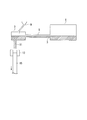
- FIG. 1 is a schematic diagram showing an outline of continuous casting when a continuous casting method is applied to casting of a Cu—Ca based alloy material in the process of manufacturing a hot rolled sheet made of a copper alloy for a sputtering target of the present invention.
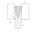
- FIG. 4 is a schematic view showing a preferred mold for applying a continuous casting method to casting of a Cu—Ca based alloy material in a vertical cross-sectional position in the process of manufacturing a hot rolled sheet made of a copper alloy for a sputtering target of the present invention.
- FIG. 3 is a schematic diagram of a Cu—Ca alloy hot-rolled sheet showing a sampling position for measuring the particle size of Cu— ⁇ phase crystal grains in a Cu substrate in an example of the present invention.
- the hot rolled sheet made of a copper alloy for a sputtering target according to the present invention is basically a copper alloy containing 0.5 to 10.0 atomic% of Ca as the component composition, with the balance being Cu and inevitable impurities.
- the hot rolled sheet made of a copper alloy for a sputtering target according to the present invention is basically a copper alloy containing 0.5 to 10.0 atomic% of Ca as the component composition, with the balance being Cu and inevitable impurities.
- a copper alloy containing 10.0 atomic% or less in total of one or more selected from the above will be described.
- Ca is a basic alloy element in the Cu—Ca based copper alloy that is the subject of the present invention, and is a Cu—Ca based copper alloy obtained by using a Cu—Ca based copper alloy as a sputtering target for TFT wiring.
- the copper alloy film not only exhibits low resistivity as a wiring layer, but also has excellent adhesion to a substrate made of glass, Si, silica, etc. Furthermore, depending on sputtering conditions, expensive Mo, Ti, etc. It is possible to reduce the cost by eliminating the need for the underlying layer, and it is possible to prevent the adhesion of the wiring film from being lowered by various heat treatments generally applied in the TFT manufacturing process.
- a hot-rolled sheet made of a Cu—Ca alloy containing Ca is used as a material for a sputtering target when such a Cu—Ca copper alloy film is formed on a substrate by sputtering. It is said.
- the Ca content of the Cu—Ca-based alloy in the hot rolled sheet made of copper alloy for a sputtering target of the present invention is set in the range of 0.5 to 10.0 atomic%.
- a melting raw material is melted in a batch type melting furnace, and only a casting is continuously performed for a certain length, and a melting raw material is continuously melted.
- the Ca content is up to about 10.0 atomic%. If it is a copper alloy, it can be cast without any problem.
- the latter continuous casting method if Ca exceeds 6.0 atomic%, casting is performed by continuous addition of a large amount of Ca-adding material at the time of melting casting. The molten metal temperature may decrease and casting may be difficult.
- Ca is preferably 6.0 atomic% or less, and further 4.0 atomic% or less. It is more preferable to do.
- the grain size of the Cu-Ca crystallized product that crystallizes during casting tends to increase.
- the particle size of the Cu—Ca-based crystallized product crystallized during casting can be reduced by appropriately controlling the solidification rate during casting.
- the average grain size of the Cu- ⁇ phase crystal grains in the Cu substrate in the hot-rolled sheet can be adjusted to be equal to or smaller than the predetermined size defined in the present invention.
- the hot-rolled sheet made of copper alloy for sputtering target of the present invention should basically be composed of a Cu—Ca alloy containing 0.5 to 10.0 atomic% of Ca as described above.
- the present invention can be applied to any Cu—Ca alloy hot rolled sheet that can be used as a sputtering target. That is, you may add the alloy element which can be added as a sputtering target material with Ca as needed.
- Typical elements include Mg, Mn, Al, and P. For these, Mg 0.1 to 5.0 atomic%, Mn 0.1 to 5.0 atomic%, Al 0.1 to 5.0 atomic% %, P 0.001 to 0.1 atomic%, and a total of 10.0 atomic% or less is permitted. Then, the selective addition element added as needed is demonstrated.
- Mg When a TFT wiring film is formed by sputtering using a target using a hot rolled plate made of an alloy obtained by adding Mg to a Cu—Ca alloy, Mg improves the barrier property of the wiring film with respect to the substrate and the substrate. This contributes to improving the adhesion to the material. If the added amount of Mg is less than 0.1 atomic%, the effect cannot be obtained sufficiently. If the added amount exceeds 5.0 atomic%, the specific resistance of the wiring film increases and becomes unsuitable as a TFT wiring film. Therefore, when Mg is added, the amount of Mg added is in the range of 0.1 to 5.0 atomic%.
- Mn When a TFT wiring film is formed by sputtering using a target using a hot rolled sheet made of an alloy obtained by adding Mn to a Cu—Ca alloy, Mn adheres to the substrate of the wiring film due to coexistence with Ca. , Improve chemical stability. If the amount of Mn added is less than 0.1 atomic%, these effects cannot be obtained sufficiently, and if it exceeds 5.0 atomic%, the specific resistance of the wiring film increases and becomes unsuitable as a TFT wiring film. Therefore, when Mn is added, the amount of Mn added is within the range of 0.1 to 5.0 atomic%.
- Al When a TFT wiring film is formed by sputtering using a target using a hot rolled plate made of an alloy obtained by adding Al to a Cu—Ca alloy, Al adheres to the substrate of the wiring film due to the coexistence with Ca. , Improve chemical stability. If the added amount of Al is less than 0.1 atomic%, these effects cannot be obtained sufficiently, and if it exceeds 5.0 atomic%, the specific resistance of the wiring film increases and becomes unsuitable as a TFT wiring film. Therefore, when Al is added, the amount of Al added is in the range of 0.1 to 5.0 atomic%.
- P is an additive element that can improve the castability without impairing the specific resistance or adhesion of the TFT wiring film. If the amount of P added is less than 0.001 atomic%, the effect is not sufficiently obtained. On the other hand, even if P is added in excess of 0.1 atomic%, no further improvement in castability is observed. The specific resistance value increases. Therefore, when P is added, the amount of P added is within the range of 0.001 to 0.1 atomic%.
- the lower limit of the addition amount of these Mg, Mn, Al, and P means the lower limit in the case of adding these elements positively, and contains the trace amount below each lower limit as an impurity. Of course, it is acceptable.
- the total content of one or more of the above Mg, Mn, Al, and P is in the range of 10.0 atomic% or less. If the total content exceeds 10.0 atomic%, the specific resistance of the wiring film becomes excessive, making it inappropriate as a TFT wiring film.
- the balance of the above elements may basically be Cu and inevitable impurities.
- Inevitable impurities include, for example, Fe, Si, Ag, S, O, C, and H. These inevitable impurities are desirably 0.3 atomic% or less in total. Further, even if Co, Cr, Be, Hg, B, Zr, etc. are contained in a total amount of up to 0.3 atomic%, they do not affect the characteristics of the present invention. It is allowed to be contained.
- the grain size condition for the Cu- ⁇ phase crystal grains in the Cu substrate is important as a hot rolled sheet made of a copper alloy for a sputtering target made of an alloy having the above component composition. That is, as described above, by appropriately regulating the average grain size of the Cu- ⁇ phase crystal grains in the Cu substrate, abnormal discharge when sputtering is performed using a target using the hot-rolled sheet Generation
- production of can be suppressed reliably and stably.
- the average grain size of the Cu- ⁇ phase crystal grains in the Cu substrate exceeds 60 ⁇ m, the proportion of coarse crystal grains as a whole increases, and abnormal discharge is likely to occur during sputtering.
- the average grain size of the Cu- ⁇ phase crystal grains is 60 ⁇ m or less, the effect of suppressing abnormal discharge during sputtering can be obtained.
- the average particle size is regulated to 40 ⁇ m or less, the occurrence of abnormal discharge can be further reliably suppressed.
- the average grain size of the Cu- ⁇ phase crystal grains in the Cu substrate is defined to be in the range of 5 ⁇ m to 60 ⁇ m.
- the particle size of the Cu- ⁇ phase crystal grains in the Cu substrate was measured by a cutting method in accordance with JIS H0501: 1986 (corresponding to a copper grain size test method, ISO 2624-1973).
- the average particle size in the range of 5 ⁇ m to 60 ⁇ m means that the hot rolled sheet has a cross section parallel to the rolling surface, a cross section perpendicular to the rolling surface and parallel to the rolling direction, and a cross section perpendicular to the rolling surface and in the rolling direction.
- the average particle size in the visual field when measured in a visual field of 500 ⁇ m ⁇ 700 ⁇ m, and the average particle size in the three cross sections is within the above range. It means that there is.
- the hot rolled plate for sputtering target in measuring the grain size of the Cu- ⁇ phase crystal grains in the Cu substrate, as shown in the examples described later, in the center in the rolling width direction and in the plate thickness direction. A sample for measurement is taken from a portion corresponding to the center, the particle diameter is measured from three directions corresponding to the three cross sections, and the average particle diameter in the visual field in the three directions is within the range defined by the present invention. If so, it can be considered that the entire hot-rolled sheet satisfies the average particle size defined in the present invention.
- a method for producing a hot rolled sheet made of a copper alloy for a sputtering target of the present invention will be described.
- a hot rolled sheet made of a copper alloy for a sputtering target of the present invention basically, a Cu—Ca based alloy having a predetermined component composition is melted and cast into a ingot by a continuous casting method. A homogenization treatment is performed as necessary, and then hot rolling is performed to obtain a copper alloy hot rolled plate for a sputtering target having a predetermined thickness.
- a sputtering target can be finally obtained by subjecting the obtained hot-rolled sheet to appropriate machining and processing into a predetermined shape and a predetermined dimension.
- the ingot structure becomes finer as the solidification rate increases.
- the ingot structure also affects the recrystallization behavior in the subsequent hot rolling process.
- the finer the ingot structure the more easily the recrystallized structure can be refined.
- increasing the solidification rate at the time of casting is advantageous for the refining of recrystallized grains at the time of hot rolling through the refining of crystallized matter in the ingot. That is, the Cu-Ca-based crystallized crystallized during casting serves as a starting point for recrystallization nucleation during recrystallization in the hot rolling process after casting, and resistance to the growth of recrystallized grains. The finer the crystallized material, the finer the recrystallized structure.
- the temperature at the time of hot rolling is also important. From these viewpoints, it is desirable to increase the solidification rate (cooling rate during casting) as much as possible when producing the copper alloy hot-rolled sheet for sputtering target of the present invention.
- a continuous casting method as a casting method capable of obtaining a high solidification rate. Therefore, in the present invention, the continuous casting method is applied.
- the continuous casting methods it is preferable to apply the complete continuous casting method from the viewpoint of productivity.
- a high-purity copper raw material such as electrolytic copper is melted in a melting furnace 1.
- the surface of the molten metal (molten copper) in the melting furnace 1 is sealed with carbon, and the atmosphere in the melting furnace 1 is an inert gas or a reducing gas.
- the molten copper 3 melted in the melting furnace 1 is continuously guided to the tundish 7 through the basket 5 sealed with an inert gas or a reducing gas.
- the tundish 7 is provided with an adding means 9 for adding an alloy element such as Ca, and an alloy element such as Ca is continuously added so as to achieve a target component composition.
- a molten copper alloy (Cu—Ca alloy) whose components are adjusted in the tundish 7 is continuously poured from the pouring nozzle 11 into the continuous casting mold 13.
- the ingot 15 solidified by the continuous casting mold 13 is continuously drawn by a drawing means such as a pinch roll (not shown).
- the size (the size of the gap between the mold inner surface and the ingot surface) is increased, heat removal from the ingot surface at that portion may be insufficient and the solidification rate may be reduced. . And depending on the shape of the mold (cross-sectional shape of the ingot to be cast) and the cooling method, such mold separation may be remarkably increased.
- the mold taper (inclination angle of the mold inner surface with respect to the vertical surface) also affects the mold separation.
- the outer dimension of the ingot becomes smaller as it goes downward in the mold due to the solidification shrinkage of the ingot regardless of the short side or the long side. Therefore, if the mold is not tapered, a large mold separation occurs in the lower part of the mold, which also causes a decrease in the solidification rate. Therefore, as shown in FIG. 2, such a problem can be avoided by giving a taper to the inner surface 13A of the mold 13 at a predetermined angle ⁇ . However, if the taper angle ⁇ is too large, the friction between the ingot surface and the mold inner surface will increase, which may make it difficult to pull out the ingot, so set the taper angle appropriately. Is desired.
- the ingot thus obtained is subjected to a homogenization treatment as necessary, and then hot-rolled to obtain a copper alloy hot-rolled plate for a sputtering target having a predetermined thickness.
- the conditions for the homogenization treatment and hot rolling are not particularly limited, and may be the same as those of a conventional copper alloy hot-rolled sheet for a sputtering target.
- the homogenization treatment is performed at a temperature of 650 to 900 ° C., for example. Heating for 4 hours is sufficient.
- the hot rolling may be performed at a recrystallization temperature or higher according to a conventional method. Specifically, for example, the rolling start temperature is 650 to 900 ° C., the rolling end temperature is 500 to 600 ° C., and the rolling rate is 70 to 95%. And it is sufficient.
- the recrystallized structure can be easily refined as the ingot structure before recrystallization is finer.
- the Cu—Ca-based crystallized product in the ingot does not dissolve in the Cu matrix, and almost the entire amount remains in the hot-rolled sheet, but the crystallized product is not recrystallized in the hot rolling process. In the above, it functions as a recrystallization nucleus, and further resists the growth of the recrystallized grains, thereby preventing the recrystallized grains from becoming coarse. Therefore, the finer the crystallized material in the ingot, the finer the recrystallized structure.
- the hot-rolled sheet made of the Cu—Ca-based alloy obtained as described above is processed into a predetermined shape and a predetermined dimension by appropriate machining or the like, a sputtering target can be finally obtained.
- the cast continuous casting ingot was divided into lengths of 950 mm, heated to the hot rolling start temperature shown in Table 1 for 2 hours by a batch-type heating furnace, and then started hot rolling until the plate thickness reached 22 mm. It rolled and water-cooled and it was set as the hot rolled sheet made from a copper alloy for sputtering targets.
- the hot rolling finish temperature was 550 ° C.
- the surface of the plate material cut out from each obtained hot-rolled plate was turned to produce a sputtering target having a dimension of an outer diameter of 200 mm ⁇ thickness of 10 mm.
- oxygen-free copper having a purity of 99.99 mass% is prepared, and the oxygen-free copper is obtained by high-frequency melting in a high-purity graphite mold in an Ar gas atmosphere.
- No. 1 in Table 1 was dissolved by adding Ca to the molten metal obtained.
- Ingredient adjustment was made so that the molten metal having the component composition shown in FIG. 11 was obtained, the obtained molten metal was cast into a cooled carbon mold, further hot-rolled to form a hot-rolled sheet, and then subjected to strain relief annealing. Then, the surface was turned to produce a sputtering target having an outer diameter of 200 mm and a thickness of 10 mm.
- samples are taken from a portion corresponding to the center in the rolling width direction and the center in the thickness direction at three points of the front end, the middle, and the rear end of the hot rolled plate 20, and parallel to the rolling surface.
- a target with a backing plate was obtained by superposing and soldering a sputtering target made of a hot rolled plate of each of 11 alloys on an oxygen-free copper backing plate.
- Each target was attached to a sputtering apparatus, and continuous sputtering was performed under the following conditions. Sputtering was performed in two types of atmospheres (Ar gas atmosphere and Ar—O 2 mixed gas atmosphere) assuming sputtering in different atmospheres.
- no. 1-No. 9 is an example of the present invention in which the average grain size of the Cu- ⁇ phase crystal grains is in the range of 5 to 60 ⁇ m.
- no. No. 10 is a comparative example in which the average grain size of the Cu- ⁇ phase crystal grains exceeded 60 ⁇ m.
- no. 11 is a conventional example manufactured by applying a batch-type casting method. In this case, the average grain size of Cu- ⁇ phase crystal grains greatly exceeds 60 ⁇ m.
- the average particle size of the Cu- ⁇ phase crystal grains is in the range of 5 to 60 ⁇ m. 1-No. It was confirmed that the number of abnormal discharges in all of the 9 inventive examples was as small as 6 or less.
- the present invention it is possible to form a wiring film having a low specific resistance and a stable adhesion to the substrate, which makes it possible to manufacture a large-sized and high-definition TFT panel.
Landscapes
- Chemical & Material Sciences (AREA)
- Engineering & Computer Science (AREA)
- Mechanical Engineering (AREA)
- Materials Engineering (AREA)
- Metallurgy (AREA)
- Organic Chemistry (AREA)
- Physics & Mathematics (AREA)
- Chemical Kinetics & Catalysis (AREA)
- Thermal Sciences (AREA)
- Crystallography & Structural Chemistry (AREA)
- Analytical Chemistry (AREA)
- Plasma & Fusion (AREA)
- Physical Vapour Deposition (AREA)
Abstract
Description
本願は、2012年12月28日に、日本に出願された特願2012-288705号に基づき優先権を主張し、その内容をここに援用する。 The present invention provides a sputtering target when a copper alloy film as a wiring film such as a gate electrode, a source electrode, and a drain electrode of a thin film transistor is formed on a substrate made of glass, amorphous Si, or silica by sputtering. In particular, the present invention relates to a sputtering target made of a copper alloy and a hot-rolled plate used for the sputtering target, and more particularly, to a sputtering target and a hot-rolled plate made of a Cu—Ca alloy (Ca-containing copper alloy). Is.
This application claims priority based on Japanese Patent Application No. 2012-288705 filed in Japan on December 28, 2012, the contents of which are incorporated herein by reference.
従来、大型、高精細のTFTパネルのゲート電極、ソース電極、ドレイン電極などの配線膜としては、アルミニウム(Al)系材料からなる配線膜を使用することが多かったが、最近では、配線膜の低抵抗化のため、Alよりも導電率が高い銅(Cu)系材料を使用することが進められている。 As is well known, a flat panel display such as a liquid crystal display or an organic EL display has a structure in which a thin film transistor (hereinafter referred to as “TFT”) is formed on a substrate such as glass. On the other hand, due to the recent demand for larger and finer flat-screen televisions, large and high-definition display panels (TFT panels) using this type of TFT have been demanded.
Conventionally, a wiring film made of an aluminum (Al) -based material has been often used as a wiring film for a gate electrode, a source electrode, a drain electrode, etc. of a large-sized, high-definition TFT panel. In order to reduce the resistance, the use of a copper (Cu) -based material having higher conductivity than Al is being promoted.
すなわち、本発明者等の実験によれば、スパッタリングターゲットを構成しているCu-Ca系合金におけるCu素地中のCu―α相の結晶粒径が大きい場合に、異常放電が発生しやすくなることが判明しているが、特許文献1、2においては、Cu素地中のCu―α相の結晶粒径については考慮されておらず、しかも特許文献1、2によるスパッタリングターゲットでは、鋳造方法としてカーボン鋳型に鋳造する方法を適用しているため、Cu―α相の結晶粒径が大きくなりやすく、このことがスパッタリング時の異常放電が発生する原因の一つとなっていると考えられる。 In Patent Documents 1 and 2, when manufacturing a sputtering target made of a Cu—Ca alloy added with Ca, a molten alloy is cast into a carbon mold, hot-rolled, and finally subjected to strain relief annealing. However, it is necessary to reliably and stably prevent the occurrence of abnormal discharge during sputtering in the sputtering target thus obtained.
That is, according to the experiments by the present inventors, abnormal discharge is likely to occur when the crystal grain size of the Cu-α phase in the Cu substrate in the Cu—Ca alloy constituting the sputtering target is large. However, in Patent Documents 1 and 2, the crystal grain size of the Cu-α phase in the Cu substrate is not considered, and the sputtering target according to Patent Documents 1 and 2 uses carbon as a casting method. Since the casting method is applied to the mold, the crystal grain size of the Cu-α phase tends to increase, which is considered to be one of the causes of abnormal discharge during sputtering.
なお、Cu―α相の結晶粒径を微細化するためには、熱間圧延後に、冷間加工や歪取り焼鈍などの適切な加工熱処理を付加することも考えられる。しかしながら、Cu-Ca系合金は、Cu-Ca系晶出物が比較的脆いため、冷間加工性が悪く、そのため実際の量産的規模でのスパッタリングターゲットの製造には適用し難いのが実状である。 The inventors have investigated and studied the cause of abnormal discharge that may occur when sputtering using a target made of a Cu—Ca alloy. It has been found that the grain size of the Cu-α phase grains in the Cu substrate has a great influence on the occurrence of abnormal discharge. That is, if the grain size of the Cu-α phase crystal grains in the Cu substrate is coarse, abnormal discharge is likely to occur. Therefore, in order to prevent the occurrence of abnormal discharge, it is desired to refine the Cu-α phase crystal grains in the Cu substrate of the sputtering target.
In order to refine the crystal grain size of the Cu-α phase, it is conceivable to add an appropriate heat treatment such as cold working or strain relief annealing after hot rolling. However, Cu-Ca alloys are poor in cold workability because Cu-Ca crystals are relatively brittle, and are therefore difficult to apply to the production of sputtering targets on an actual mass production scale. is there.
本発明のスパッタリングターゲット用銅合金製熱間圧延板は、その成分組成として、基本的には、Caを0.5~10.0原子%含有し、残部がCuおよび不可避的不純物よりなる銅合金からなるものであり、さらに必要に応じて、Mg0.1~5.0原子%、Mn0.1~5.0原子%、Al0.1~5.0原子%、P0.001~0.1原子%のうちから選ばれた1種以上を、合計で10.0原子%以下含有する銅合金からなるものである。
そこで先ずこのような銅合金の成分組成の限定理由について説明する。 Hereinafter, the copper alloy hot-rolled sheet for sputtering target of the present invention and the sputtering target using the same will be described in more detail.
The hot rolled sheet made of a copper alloy for a sputtering target according to the present invention is basically a copper alloy containing 0.5 to 10.0 atomic% of Ca as the component composition, with the balance being Cu and inevitable impurities. As needed, Mg 0.1 to 5.0 atomic%, Mn 0.1 to 5.0 atomic%, Al 0.1 to 5.0 atomic%, P 0.001 to 0.1 atomic %, A copper alloy containing 10.0 atomic% or less in total of one or more selected from the above.
First, the reasons for limiting the component composition of such a copper alloy will be described.
Caは、本発明で対象としているCu-Ca系の銅合金において基本的な合金元素であり、TFT配線のためにスパッタリングターゲットとしてCu-Ca系の銅合金を用いて得られるCu-Ca系の銅合金膜は、配線層として比抵抗が低いという特性を示すばかりでなく、ガラスやSi、シリカなどからなる基板に対する密着性が優れており、さらにはスパッタリング条件などによっては高価なMoやTiなどからなる下地層を不要として低コスト化を図ることが可能であり、またTFT作成過程で一般に適用されている各種熱処理によって配線膜の密着性が低下してしまうことを防止できる。そこで本発明では、このようなCu-Ca系の銅合金膜を基板上にスパッタリングによって形成する際のスパッタリングターゲットの素材として、Caを含有するCu-Ca系合金からなる熱間圧延板を用いることとしている。 Ca 0.5-10.0 atomic%:
Ca is a basic alloy element in the Cu—Ca based copper alloy that is the subject of the present invention, and is a Cu—Ca based copper alloy obtained by using a Cu—Ca based copper alloy as a sputtering target for TFT wiring. The copper alloy film not only exhibits low resistivity as a wiring layer, but also has excellent adhesion to a substrate made of glass, Si, silica, etc. Furthermore, depending on sputtering conditions, expensive Mo, Ti, etc. It is possible to reduce the cost by eliminating the need for the underlying layer, and it is possible to prevent the adhesion of the wiring film from being lowered by various heat treatments generally applied in the TFT manufacturing process. Accordingly, in the present invention, a hot-rolled sheet made of a Cu—Ca alloy containing Ca is used as a material for a sputtering target when such a Cu—Ca copper alloy film is formed on a substrate by sputtering. It is said.
Cu-Ca合金にMgを添加した合金からなる熱間圧延板を使用したターゲットを用いてスパッタリングし、TFT配線膜を形成した場合、Mgは、配線膜の基板に対するバリヤ性を向上させるとともに、基板に対する密着性を向上させるために寄与する。Mg添加量が0.1原子%未満では、その効果が充分に得られず、5.0原子%を越えれば、配線膜の比抵抗が大きくなってTFT配線膜として不適当となる。したがってMgを添加する場合のMg添加量は、0.1~5.0原子%の範囲内とした。 Mg:
When a TFT wiring film is formed by sputtering using a target using a hot rolled plate made of an alloy obtained by adding Mg to a Cu—Ca alloy, Mg improves the barrier property of the wiring film with respect to the substrate and the substrate. This contributes to improving the adhesion to the material. If the added amount of Mg is less than 0.1 atomic%, the effect cannot be obtained sufficiently. If the added amount exceeds 5.0 atomic%, the specific resistance of the wiring film increases and becomes unsuitable as a TFT wiring film. Therefore, when Mg is added, the amount of Mg added is in the range of 0.1 to 5.0 atomic%.
Cu-Ca合金にMnを添加した合金からなる熱間圧延板を使用したターゲットを用いてスパッタリングし、TFT配線膜を形成した場合、Mnは、Caとの共存により、配線膜の基板に対する密着性、化学的安定性を向上させる。Mn添加量が0.1原子%未満では、これらの効果が充分に得られず、5.0原子%を越えれば、配線膜の比抵抗が大きくなってTFT配線膜として不適当となる。したがってMnを添加する場合のMn添加量は、0.1~5.0原子%の範囲内とした。 Mn:
When a TFT wiring film is formed by sputtering using a target using a hot rolled sheet made of an alloy obtained by adding Mn to a Cu—Ca alloy, Mn adheres to the substrate of the wiring film due to coexistence with Ca. , Improve chemical stability. If the amount of Mn added is less than 0.1 atomic%, these effects cannot be obtained sufficiently, and if it exceeds 5.0 atomic%, the specific resistance of the wiring film increases and becomes unsuitable as a TFT wiring film. Therefore, when Mn is added, the amount of Mn added is within the range of 0.1 to 5.0 atomic%.
Cu-Ca合金にAlを添加した合金からなる熱間圧延板を使用したターゲットを用いてスパッタリングし、TFT配線膜を形成した場合、Alは、Caとの共存により、配線膜の基板に対する密着性、化学的安定性を向上させる。Al添加量が0.1原子%未満では、これらの効果が充分に得られず、5.0原子%を越えれば、配線膜の比抵抗が大きくなってTFT配線膜として不適当となる。したがってAlを添加する場合のAl添加量は、0.1~5.0原子%の範囲内とした。 Al:
When a TFT wiring film is formed by sputtering using a target using a hot rolled plate made of an alloy obtained by adding Al to a Cu—Ca alloy, Al adheres to the substrate of the wiring film due to the coexistence with Ca. , Improve chemical stability. If the added amount of Al is less than 0.1 atomic%, these effects cannot be obtained sufficiently, and if it exceeds 5.0 atomic%, the specific resistance of the wiring film increases and becomes unsuitable as a TFT wiring film. Therefore, when Al is added, the amount of Al added is in the range of 0.1 to 5.0 atomic%.
Pは、TFT配線膜の比抵抗や密着性などを損なうことなく鋳造性を向上させることが可能な添加元素である。P添加量が0.001原子%未満では、その効果が充分に得られず、一方0.1原子%を越えてPを添加しても、それ以上の鋳造性の向上効果は認められず、比抵抗値が上昇してしまう。そこでPを添加する場合のP添加量は、0.001~0.1原子%の範囲内とした。 P:
P is an additive element that can improve the castability without impairing the specific resistance or adhesion of the TFT wiring film. If the amount of P added is less than 0.001 atomic%, the effect is not sufficiently obtained. On the other hand, even if P is added in excess of 0.1 atomic%, no further improvement in castability is observed. The specific resistance value increases. Therefore, when P is added, the amount of P added is within the range of 0.001 to 0.1 atomic%.
なおまた、上記のMg、Mn、Al、Pの1種以上の合計含有量は、10.0原子%以下の範囲内とする。これらの合計含有量が10.0原子%を越えれば、配線膜の比抵抗が過大となって、TFT配線膜として不適切となる。 In addition, the lower limit of the addition amount of these Mg, Mn, Al, and P means the lower limit in the case of adding these elements positively, and contains the trace amount below each lower limit as an impurity. Of course, it is acceptable.
In addition, the total content of one or more of the above Mg, Mn, Al, and P is in the range of 10.0 atomic% or less. If the total content exceeds 10.0 atomic%, the specific resistance of the wiring film becomes excessive, making it inappropriate as a TFT wiring film.
すなわち、既に述べたように、Cu素地中のCu―α相結晶粒の平均粒径を適切に規制することによって、その熱間圧延板を使用したターゲットを用いてスパッタリングを行なった場合の異常放電の発生を、確実かつ安定して抑制することができる。 In the present invention, the grain size condition for the Cu-α phase crystal grains in the Cu substrate is important as a hot rolled sheet made of a copper alloy for a sputtering target made of an alloy having the above component composition.
That is, as described above, by appropriately regulating the average grain size of the Cu-α phase crystal grains in the Cu substrate, abnormal discharge when sputtering is performed using a target using the hot-rolled sheet Generation | occurrence | production of can be suppressed reliably and stably.
一方Cu―α相結晶粒の平均粒径が60μm以下であれば、スパッタリング時の異常放電を抑える効果が得られる。なお平均粒径を40μm以下に規制すれば、より一層異常放電の発生を確実に抑制することが可能となる。一方Cu―α相結晶粒の平均粒径を5μm未満に調整することは、鋳造時の冷却速度との関係から、量産的規模での通常の完全連続鋳造もしくは半連続鋳造では困難であり、したがって平均粒径を5μm未満に規制しようとすれば、特殊な鋳造方案、冷却方案が必要となって、著しいコスト上昇を招いてしまう。
そこでこの発明では、Cu素地中のCu―α相結晶粒の平均粒径を5μm~60μmの範囲内と規定した。 Here, if the average grain size of the Cu-α phase crystal grains in the Cu substrate exceeds 60 μm, the proportion of coarse crystal grains as a whole increases, and abnormal discharge is likely to occur during sputtering.
On the other hand, if the average grain size of the Cu-α phase crystal grains is 60 μm or less, the effect of suppressing abnormal discharge during sputtering can be obtained. If the average particle size is regulated to 40 μm or less, the occurrence of abnormal discharge can be further reliably suppressed. On the other hand, it is difficult to adjust the average grain size of the Cu-α phase crystal grains to less than 5 μm in the normal full continuous casting or semi-continuous casting on a mass production scale because of the relationship with the cooling rate during casting. If the average particle size is to be regulated to less than 5 μm, a special casting method and cooling method are required, which causes a significant increase in cost.
Therefore, in the present invention, the average grain size of the Cu-α phase crystal grains in the Cu substrate is defined to be in the range of 5 μm to 60 μm.
本発明のスパッタリングターゲット用銅合金製熱間圧延板を製造するに当たっては、基本的には、所定の成分組成のCu-Ca系合金を溶製し、連続鋳造法により鋳造して鋳塊とし、必要に応じて均質化処理を行ってから、熱間圧延を施して、所定の板厚のスパッタリングターゲット用銅合金製熱間圧延板とする。得られた熱間圧延板に対し、適宜機械加工などを施して所定の形状、所定の寸法に加工することによって、最終的にスパッタリングターゲットを得ることができる。 Next, a method for producing a hot rolled sheet made of a copper alloy for a sputtering target of the present invention will be described.
In producing a hot rolled sheet made of a copper alloy for a sputtering target of the present invention, basically, a Cu—Ca based alloy having a predetermined component composition is melted and cast into a ingot by a continuous casting method. A homogenization treatment is performed as necessary, and then hot rolling is performed to obtain a copper alloy hot rolled plate for a sputtering target having a predetermined thickness. A sputtering target can be finally obtained by subjecting the obtained hot-rolled sheet to appropriate machining and processing into a predetermined shape and a predetermined dimension.
また鋳造時の凝固速度を高めることは、鋳塊中の晶出物の微細化を通じての、熱間圧延時の再結晶粒の微細化にも有利となる。すなわち、鋳造時に晶出したCu-Ca系晶出物は、鋳造後の熱間圧延工程における再結晶時に、再結晶核生成の起点となるとともに、再結晶粒の成長に対する抵抗となることから、晶出物が微細であるほど、再結晶組織が微細化される。なお、熱間圧延時の温度が高すぎると再結晶が粗大化してしまうことから、熱間圧延時の温度も重要となる。
これらの観点から、本発明のスパッタリングターゲット用銅合金製熱間圧延板を製造する場合も、凝固速度(鋳造時の冷却速度)をできるだけ高くすることが望まれる。スパッタリングターゲット用銅合金製熱間圧延板を量産的規模で製造する場合において、大きい凝固速度が得られる鋳造方法としては、連続鋳造法がある。そこで本発明においても、連続鋳造法を適用することとした。なお連続鋳造法のうちでも、生産性の面からは、完全連続鋳造法を適用することが好ましい。 During casting, the ingot structure becomes finer as the solidification rate increases. The ingot structure also affects the recrystallization behavior in the subsequent hot rolling process. In general, the finer the ingot structure, the more easily the recrystallized structure can be refined.
Further, increasing the solidification rate at the time of casting is advantageous for the refining of recrystallized grains at the time of hot rolling through the refining of crystallized matter in the ingot. That is, the Cu-Ca-based crystallized crystallized during casting serves as a starting point for recrystallization nucleation during recrystallization in the hot rolling process after casting, and resistance to the growth of recrystallized grains. The finer the crystallized material, the finer the recrystallized structure. In addition, since the recrystallization will coarsen when the temperature at the time of hot rolling is too high, the temperature at the time of hot rolling is also important.
From these viewpoints, it is desirable to increase the solidification rate (cooling rate during casting) as much as possible when producing the copper alloy hot-rolled sheet for sputtering target of the present invention. In the case of producing a copper alloy hot rolled plate for sputtering target on a mass production scale, there is a continuous casting method as a casting method capable of obtaining a high solidification rate. Therefore, in the present invention, the continuous casting method is applied. Of the continuous casting methods, it is preferable to apply the complete continuous casting method from the viewpoint of productivity.
また鋳塊中のCu-Ca系晶出物はCuマトリックス中に固溶せず、ほぼ全量が、熱間圧延板中に残るが、その晶出物は、熱間圧延工程での再結晶時において、再結晶核として機能し、さらに再結晶粒の成長に対する抵抗となることによって、再結晶粒の粗大化を防止する。したがって鋳塊中の晶出物が微細であるほど、再結晶組織が微細化される。
このように、鋳造方法として連続鋳造法を適用し、鋳造時の凝固速度を大きくして鋳塊組織の微細化と晶出物の微細化を図っておくことによって、熱間圧延工程における再結晶粒の微細化、再結晶粒の粗大化防止を容易に達成し、熱間圧延板におけるCu素地中のCu―α相結晶粒を微細化して、そのCu―α相結晶粒の平均粒径を前述の範囲内に収めることが可能となる。 Although recrystallization occurs in the hot rolling process, the recrystallized structure can be easily refined as the ingot structure before recrystallization is finer.
In addition, the Cu—Ca-based crystallized product in the ingot does not dissolve in the Cu matrix, and almost the entire amount remains in the hot-rolled sheet, but the crystallized product is not recrystallized in the hot rolling process. In the above, it functions as a recrystallization nucleus, and further resists the growth of the recrystallized grains, thereby preventing the recrystallized grains from becoming coarse. Therefore, the finer the crystallized material in the ingot, the finer the recrystallized structure.
In this way, by applying the continuous casting method as the casting method and increasing the solidification rate at the time of casting to refine the ingot structure and the crystallized material, recrystallization in the hot rolling process Easily achieve grain refinement and prevention of coarsening of recrystallized grains, refine the Cu-α phase grains in the Cu substrate in the hot rolled sheet, and increase the average grain size of the Cu-α phase grains It becomes possible to be within the above-mentioned range.
鋳造された連続鋳造鋳塊は、長さ950mmに分断して、バッチ式加熱炉により表1に記載の熱間圧延開始温度に2時間加熱してから熱間圧延を開始し、板厚22mmまで圧延して水冷し、スパッタリングターゲット用銅合金製熱間圧延板とした。熱間圧延終了温度は550℃とした。
得られた各熱間圧延板から切り出した板材の表面を旋盤加工して、外径200mm×厚さ10mmの寸法を有するスパッタリングターゲットを作製した。 Using the continuous casting apparatus shown in FIG. 1, electrolytic copper having a purity of 99.99% by mass was dissolved, and Ca was added to the molten copper by the adding means 9, so that No. 1 of the present invention in Table 1 was obtained. 1-No. 9 and Comparative Example No. A Cu—Ca alloy having the composition shown in FIG. 10 was cast. The ingot was a cake-like ingot having a rectangular cross section, and the cross-sectional dimension was 260 mm × 640 mm. In casting, a mold made of carbon was used, and the amount of cooling water was 2,500 liters / minute. The taper of the mold was 0.4 ° on the long side and 0.4 ° on the short side. The drawing speed was about 9 cm / min.
The cast continuous casting ingot was divided into lengths of 950 mm, heated to the hot rolling start temperature shown in Table 1 for 2 hours by a batch-type heating furnace, and then started hot rolling until the plate thickness reached 22 mm. It rolled and water-cooled and it was set as the hot rolled sheet made from a copper alloy for sputtering targets. The hot rolling finish temperature was 550 ° C.
The surface of the plate material cut out from each obtained hot-rolled plate was turned to produce a sputtering target having a dimension of an outer diameter of 200 mm × thickness of 10 mm.
No.1~No.11の各熱間圧延板のサンプルについての、Cu素地中のCu―α相結晶粒の平均粒径を、表1中に示す。 In the above process, a sample for observing the crystal grain size was taken from each hot rolled plate. As shown in FIG. 3, samples are taken from a portion corresponding to the center in the rolling width direction and the center in the thickness direction at three points of the front end, the middle, and the rear end of the hot rolled
No. 1-No. Table 1 shows the average grain size of the Cu-α phase crystal grains in the Cu substrate for each of the 11 hot-rolled plate samples.
各ターゲットをスパッタ装置に取り付けて、次のような条件で連続スパッタを行なった。なおスパッタは、異なる雰囲気でのスパッタを想定して、2種類の雰囲気(Arガス雰囲気と、Ar-O2混合ガス雰囲気)で実施した。
電源:直流方式
スパッタ出力:600W
到達真空度:4×10⁻⁵ Pa
雰囲気ガス組成:Arガス、Ar:90容量%と酸素:10容量%の混合ガスの2種類
(Arガス:配線膜としてのスパッタ。混合ガス:酸素含有膜としてのスパッタ)
スパッタ圧:0.2Pa
スパッタ時間:8時間
この連続スパッタの間には、電源に付属するアーキングカウンターを用いて、総異常放電回数をカウントした。その結果を表1に示す。 On the other hand, No. obtained as described above. 1-No. A target with a backing plate was obtained by superposing and soldering a sputtering target made of a hot rolled plate of each of 11 alloys on an oxygen-free copper backing plate.
Each target was attached to a sputtering apparatus, and continuous sputtering was performed under the following conditions. Sputtering was performed in two types of atmospheres (Ar gas atmosphere and Ar—O 2 mixed gas atmosphere) assuming sputtering in different atmospheres.
Power supply: DC method Sputter output: 600W
Ultimate vacuum: 4 × 10 −5 Pa
Atmospheric gas composition: Ar gas, Ar: 90% by volume and oxygen: 10% by volume of mixed gas (Ar gas: sputtering as a wiring film; mixed gas: sputtering as an oxygen-containing film)
Sputtering pressure: 0.2Pa
Sputtering time: 8 hours During this continuous sputtering, the total number of abnormal discharges was counted using an arcing counter attached to the power source. The results are shown in Table 1.

一方No.10は、Cu―α相結晶粒の平均粒径が60μmを越えた比較例である。
さらにNo.11は、バッチ式の鋳造方法を適用して製造された従来例であり、この場合は、Cu―α相結晶粒の平均粒径が60μmを大幅に越えている。 In Table 1, no. 1-No. 9 is an example of the present invention in which the average grain size of the Cu-α phase crystal grains is in the range of 5 to 60 μm.
On the other hand, no. No. 10 is a comparative example in which the average grain size of the Cu-α phase crystal grains exceeded 60 μm.
Furthermore, no. 11 is a conventional example manufactured by applying a batch-type casting method. In this case, the average grain size of Cu-α phase crystal grains greatly exceeds 60 μm.
3 溶銅
7 タンディッシュ
13 鋳型
15 鋳塊 1 Melting furnace 3
Claims (4)
- 連続鋳造法により鋳造した鋳塊を熱間圧延してなる熱間圧延板であって、
Caを0.5~10.0原子%含有し、残部がCuおよび不可避的不純物よりなる銅合金からなり、かつCu素地中のCu―α相結晶粒の平均粒径が、5~60μmの範囲内にあることを特徴とするスパッタリングターゲット用銅合金製熱間圧延板。 A hot-rolled sheet obtained by hot rolling an ingot cast by a continuous casting method,
Containing 0.5 to 10.0 atomic% of Ca, the balance being made of a copper alloy consisting of Cu and inevitable impurities, and the average grain size of Cu-α phase crystal grains in the Cu substrate being in the range of 5 to 60 μm A hot-rolled sheet made of copper alloy for a sputtering target, wherein the hot-rolled sheet is for a sputtering target. - 請求項1に記載のスパッタリングターゲット用銅合金製熱間圧延板において、前記銅合金におけるCa含有量が、0.5~6.0原子%の範囲内にあることを特徴とするスパッタリングターゲット用銅合金製熱間圧延板。 2. The hot rolled sheet for a copper alloy for a sputtering target according to claim 1, wherein the Ca content in the copper alloy is in the range of 0.5 to 6.0 atomic%. Alloy hot rolled sheet.
- 請求項1、請求項2のうちのいずれかの請求項に記載のスパッタリングターゲット用銅合金製熱間圧延板において、前記銅合金が、さらにMg0.1~5.0原子%、Mn0.1~5.0原子%、Al0.1~5.0原子%、P0.001~0.1原子%のうちから選ばれた1種以上を、合計で10.0原子%以下含有することを特徴とするスパッタリングターゲット用銅合金製熱間圧延板。 The hot rolled sheet made of a copper alloy for a sputtering target according to any one of claims 1 and 2, wherein the copper alloy further comprises Mg 0.1 to 5.0 atomic%, Mn 0.1 to It is characterized by containing one or more selected from 5.0 atomic%, Al 0.1 to 5.0 atomic%, and P 0.001 to 0.1 atomic% in total of 10.0 atomic% or less. A hot rolled sheet made of copper alloy for a sputtering target.
- 請求項1~請求項3のうちのいずれかの請求項に記載のスパッタリングターゲット用銅合金製熱間圧延板からなることを特徴とするスパッタリングターゲット。 A sputtering target comprising the copper alloy hot-rolled plate for a sputtering target according to any one of claims 1 to 3.
Priority Applications (4)
| Application Number | Priority Date | Filing Date | Title |
|---|---|---|---|
| KR1020157015387A KR101644283B1 (en) | 2012-12-28 | 2013-12-03 | Hot rolled copper alloy sheet for sputtering target, and sputtering target |
| CN201380061284.9A CN104812920B (en) | 2012-12-28 | 2013-12-03 | Sputtering target copper alloy hot rolled plate and sputtering target |
| HK15110441.7A HK1209802A1 (en) | 2012-12-28 | 2013-12-03 | Hot rolled copper alloy sheet for sputtering target, and sputtering target |
| US14/654,210 US9437405B2 (en) | 2012-12-28 | 2013-12-03 | Hot rolled plate made of copper alloy used for a sputtering target and sputtering target |
Applications Claiming Priority (2)
| Application Number | Priority Date | Filing Date | Title |
|---|---|---|---|
| JP2012288705A JP5842806B2 (en) | 2012-12-28 | 2012-12-28 | Copper alloy hot rolled plate for sputtering target and sputtering target |
| JP2012-288705 | 2012-12-28 |
Publications (1)
| Publication Number | Publication Date |
|---|---|
| WO2014103626A1 true WO2014103626A1 (en) | 2014-07-03 |
Family
ID=51020720
Family Applications (1)
| Application Number | Title | Priority Date | Filing Date |
|---|---|---|---|
| PCT/JP2013/082439 WO2014103626A1 (en) | 2012-12-28 | 2013-12-03 | Hot rolled copper alloy sheet for sputtering target, and sputtering target |
Country Status (7)
| Country | Link |
|---|---|
| US (1) | US9437405B2 (en) |
| JP (1) | JP5842806B2 (en) |
| KR (1) | KR101644283B1 (en) |
| CN (1) | CN104812920B (en) |
| HK (1) | HK1209802A1 (en) |
| TW (1) | TWI545210B (en) |
| WO (1) | WO2014103626A1 (en) |
Families Citing this family (1)
| Publication number | Priority date | Publication date | Assignee | Title |
|---|---|---|---|---|
| JP6274026B2 (en) * | 2013-07-31 | 2018-02-07 | 三菱マテリアル株式会社 | Copper alloy sputtering target and method for producing copper alloy sputtering target |
Citations (9)
| Publication number | Priority date | Publication date | Assignee | Title |
|---|---|---|---|---|
| JPH05311424A (en) * | 1992-05-12 | 1993-11-22 | Dowa Mining Co Ltd | Sputtering target for forming thin metal film and its production |
| JPH11158614A (en) * | 1997-11-28 | 1999-06-15 | Hitachi Metals Ltd | Copper target for sputtering and its production |
| JP2008506040A (en) * | 2004-07-15 | 2008-02-28 | プランゼー エスエー | Materials for conductive wires made from copper alloys |
| JP2009215613A (en) * | 2008-03-11 | 2009-09-24 | Mitsubishi Materials Corp | METHOD FOR DEPOSITING COPPER ALLOY COMPOUND FILM HAVING EXCELLENT ADHESIVENESS, AND Ca-CONTAINING COPPER ALLOY TARGET TO BE USED IN THE METHOD |
| WO2010047105A1 (en) * | 2008-10-24 | 2010-04-29 | 三菱マテリアル株式会社 | Sputtering target for forming thin film transistor wiring film |
| JP2011127160A (en) * | 2009-12-16 | 2011-06-30 | Hitachi Cable Ltd | Sputtering target material |
| WO2011078188A1 (en) * | 2009-12-22 | 2011-06-30 | 三菱伸銅株式会社 | Manufacturing method of pure copper plates, and pure copper plate |
| JP2013014808A (en) * | 2011-07-05 | 2013-01-24 | Mitsubishi Materials Corp | Copper alloy-made sputtering target |
| JP2013253309A (en) * | 2012-06-08 | 2013-12-19 | Sh Copper Products Co Ltd | Cu-Mn ALLOY SPUTTERING TARGET, LAMINATED WIRING OF SEMICONDUCTOR ELEMENT USING THE SAME, AND METHOD FOR MANUFACTURING LAMINATED WIRING |
Family Cites Families (4)
| Publication number | Priority date | Publication date | Assignee | Title |
|---|---|---|---|---|
| JPS62158841A (en) * | 1986-01-07 | 1987-07-14 | Mitsui Eng & Shipbuild Co Ltd | Alloy for superconducting material and its refining method |
| TW505705B (en) | 1996-09-09 | 2002-10-11 | Toto Ltd | Copper alloy and method of manufacturing same |
| JP5354781B2 (en) | 2009-03-11 | 2013-11-27 | 三菱マテリアル株式会社 | Thin film transistor having barrier layer as constituent layer and Cu alloy sputtering target used for sputtering film formation of said barrier layer |
| JP5201109B2 (en) * | 2009-09-16 | 2013-06-05 | 住友金属鉱山株式会社 | Method for producing porous electrode for electrolytic capacitor |
-
2012
- 2012-12-28 JP JP2012288705A patent/JP5842806B2/en active Active
-
2013
- 2013-12-03 WO PCT/JP2013/082439 patent/WO2014103626A1/en active Application Filing
- 2013-12-03 US US14/654,210 patent/US9437405B2/en active Active
- 2013-12-03 KR KR1020157015387A patent/KR101644283B1/en active Active
- 2013-12-03 HK HK15110441.7A patent/HK1209802A1/en unknown
- 2013-12-03 CN CN201380061284.9A patent/CN104812920B/en active Active
- 2013-12-17 TW TW102146641A patent/TWI545210B/en active
Patent Citations (9)
| Publication number | Priority date | Publication date | Assignee | Title |
|---|---|---|---|---|
| JPH05311424A (en) * | 1992-05-12 | 1993-11-22 | Dowa Mining Co Ltd | Sputtering target for forming thin metal film and its production |
| JPH11158614A (en) * | 1997-11-28 | 1999-06-15 | Hitachi Metals Ltd | Copper target for sputtering and its production |
| JP2008506040A (en) * | 2004-07-15 | 2008-02-28 | プランゼー エスエー | Materials for conductive wires made from copper alloys |
| JP2009215613A (en) * | 2008-03-11 | 2009-09-24 | Mitsubishi Materials Corp | METHOD FOR DEPOSITING COPPER ALLOY COMPOUND FILM HAVING EXCELLENT ADHESIVENESS, AND Ca-CONTAINING COPPER ALLOY TARGET TO BE USED IN THE METHOD |
| WO2010047105A1 (en) * | 2008-10-24 | 2010-04-29 | 三菱マテリアル株式会社 | Sputtering target for forming thin film transistor wiring film |
| JP2011127160A (en) * | 2009-12-16 | 2011-06-30 | Hitachi Cable Ltd | Sputtering target material |
| WO2011078188A1 (en) * | 2009-12-22 | 2011-06-30 | 三菱伸銅株式会社 | Manufacturing method of pure copper plates, and pure copper plate |
| JP2013014808A (en) * | 2011-07-05 | 2013-01-24 | Mitsubishi Materials Corp | Copper alloy-made sputtering target |
| JP2013253309A (en) * | 2012-06-08 | 2013-12-19 | Sh Copper Products Co Ltd | Cu-Mn ALLOY SPUTTERING TARGET, LAMINATED WIRING OF SEMICONDUCTOR ELEMENT USING THE SAME, AND METHOD FOR MANUFACTURING LAMINATED WIRING |
Also Published As
| Publication number | Publication date |
|---|---|
| KR101644283B1 (en) | 2016-07-29 |
| US9437405B2 (en) | 2016-09-06 |
| KR20150099737A (en) | 2015-09-01 |
| JP2014129580A (en) | 2014-07-10 |
| CN104812920B (en) | 2016-11-02 |
| JP5842806B2 (en) | 2016-01-13 |
| HK1209802A1 (en) | 2016-04-08 |
| US20150318153A1 (en) | 2015-11-05 |
| CN104812920A (en) | 2015-07-29 |
| TWI545210B (en) | 2016-08-11 |
| TW201439343A (en) | 2014-10-16 |
Similar Documents
| Publication | Publication Date | Title |
|---|---|---|
| JP7033664B2 (en) | Manufacturing method of 1XXX cathode foil for aluminum electrolytic capacitors | |
| JP5708315B2 (en) | Copper alloy sputtering target | |
| EP2772327B1 (en) | High-purity titanium ingots, manufacturing method therefor, and titanium sputtering target | |
| KR20210029744A (en) | Copper alloy sputtering target and manufacturing method of copper alloy sputtering target | |
| JP2016216752A (en) | Aluminum foil and manufacturing method therefor | |
| JP5842806B2 (en) | Copper alloy hot rolled plate for sputtering target and sputtering target | |
| WO2018163861A1 (en) | Cu-Ni ALLOY SPUTTERING TARGET AND PRODUCTION METHOD THEREFOR | |
| JP2007063621A (en) | Sputtering target material, method for producing aluminum material for sputtering target material, and aluminum material for sputtering target material | |
| JP6678528B2 (en) | Indium target member and method of manufacturing the same | |
| JP6331824B2 (en) | Copper alloy sputtering target | |
| JP2011102435A (en) | Sputtering target material, method for producing aluminum material for sputtering target material, and aluminum material for sputtering target material | |
| CN114959595B (en) | High-purity aluminum neodymium alloy target material for sputtering and manufacturing method thereof | |
| JP2017048446A (en) | Target material and wiring film | |
| JP5510812B2 (en) | Cu alloy film for wiring film and sputtering target material for forming wiring film |
Legal Events
| Date | Code | Title | Description |
|---|---|---|---|
| 121 | Ep: the epo has been informed by wipo that ep was designated in this application |
Ref document number: 13869397 Country of ref document: EP Kind code of ref document: A1 |
|
| ENP | Entry into the national phase |
Ref document number: 20157015387 Country of ref document: KR Kind code of ref document: A |
|
| WWE | Wipo information: entry into national phase |
Ref document number: 14654210 Country of ref document: US |
|
| NENP | Non-entry into the national phase |
Ref country code: DE |
|
| 122 | Ep: pct application non-entry in european phase |
Ref document number: 13869397 Country of ref document: EP Kind code of ref document: A1 |