WO2014103175A1 - Distortion-compensation device and distortion-compensation method - Google Patents
Distortion-compensation device and distortion-compensation method Download PDFInfo
- Publication number
- WO2014103175A1 WO2014103175A1 PCT/JP2013/007043 JP2013007043W WO2014103175A1 WO 2014103175 A1 WO2014103175 A1 WO 2014103175A1 JP 2013007043 W JP2013007043 W JP 2013007043W WO 2014103175 A1 WO2014103175 A1 WO 2014103175A1
- Authority
- WO
- WIPO (PCT)
- Prior art keywords
- coefficient
- distortion
- input signal
- signal
- compensation
- Prior art date
Links
Images

Classifications
-
- H—ELECTRICITY
- H03—ELECTRONIC CIRCUITRY
- H03F—AMPLIFIERS
- H03F1/00—Details of amplifiers with only discharge tubes, only semiconductor devices or only unspecified devices as amplifying elements
- H03F1/32—Modifications of amplifiers to reduce non-linear distortion
- H03F1/3241—Modifications of amplifiers to reduce non-linear distortion using predistortion circuits
- H03F1/3247—Modifications of amplifiers to reduce non-linear distortion using predistortion circuits using feedback acting on predistortion circuits
-
- H—ELECTRICITY
- H03—ELECTRONIC CIRCUITRY
- H03F—AMPLIFIERS
- H03F1/00—Details of amplifiers with only discharge tubes, only semiconductor devices or only unspecified devices as amplifying elements
- H03F1/32—Modifications of amplifiers to reduce non-linear distortion
- H03F1/3241—Modifications of amplifiers to reduce non-linear distortion using predistortion circuits
-
- H—ELECTRICITY
- H03—ELECTRONIC CIRCUITRY
- H03F—AMPLIFIERS
- H03F3/00—Amplifiers with only discharge tubes or only semiconductor devices as amplifying elements
- H03F3/189—High frequency amplifiers, e.g. radio frequency amplifiers
-
- H—ELECTRICITY
- H03—ELECTRONIC CIRCUITRY
- H03F—AMPLIFIERS
- H03F3/00—Amplifiers with only discharge tubes or only semiconductor devices as amplifying elements
- H03F3/189—High frequency amplifiers, e.g. radio frequency amplifiers
- H03F3/19—High frequency amplifiers, e.g. radio frequency amplifiers with semiconductor devices only
-
- H—ELECTRICITY
- H03—ELECTRONIC CIRCUITRY
- H03F—AMPLIFIERS
- H03F3/00—Amplifiers with only discharge tubes or only semiconductor devices as amplifying elements
- H03F3/20—Power amplifiers, e.g. Class B amplifiers, Class C amplifiers
- H03F3/24—Power amplifiers, e.g. Class B amplifiers, Class C amplifiers of transmitter output stages
-
- H—ELECTRICITY
- H04—ELECTRIC COMMUNICATION TECHNIQUE
- H04B—TRANSMISSION
- H04B1/00—Details of transmission systems, not covered by a single one of groups H04B3/00 - H04B13/00; Details of transmission systems not characterised by the medium used for transmission
- H04B1/02—Transmitters
- H04B1/04—Circuits
- H04B1/0475—Circuits with means for limiting noise, interference or distortion
-
- H—ELECTRICITY
- H03—ELECTRONIC CIRCUITRY
- H03F—AMPLIFIERS
- H03F2200/00—Indexing scheme relating to amplifiers
- H03F2200/451—Indexing scheme relating to amplifiers the amplifier being a radio frequency amplifier
-
- H—ELECTRICITY
- H03—ELECTRONIC CIRCUITRY
- H03F—AMPLIFIERS
- H03F2201/00—Indexing scheme relating to details of amplifiers with only discharge tubes, only semiconductor devices or only unspecified devices as amplifying elements covered by H03F1/00
- H03F2201/32—Indexing scheme relating to modifications of amplifiers to reduce non-linear distortion
- H03F2201/3224—Predistortion being done for compensating memory effects
-
- H—ELECTRICITY
- H04—ELECTRIC COMMUNICATION TECHNIQUE
- H04B—TRANSMISSION
- H04B1/00—Details of transmission systems, not covered by a single one of groups H04B3/00 - H04B13/00; Details of transmission systems not characterised by the medium used for transmission
- H04B1/02—Transmitters
- H04B1/04—Circuits
- H04B2001/0408—Circuits with power amplifiers
- H04B2001/0425—Circuits with power amplifiers with linearisation using predistortion
Definitions
- the present invention relates to a distortion compensation apparatus and a distortion compensation method for compensating for distortion of an output signal output from a predetermined circuit.
- the inverse characteristics of analog circuits and RF circuits are stored in a LUT (Look Up Table) as compensation coefficients according to the amplitude and power of the input signal.
- distortion compensation is implement
- the input signal to which the compensation coefficient is applied is compared with the transmission signal, and the compensation coefficient is adaptively updated so that the difference is reduced.
- Patent Document 1 discloses a technique for generating a compensation coefficient for compensating for signal distortion by an adaptive algorithm based on a difference between an input signal and an output signal of the amplifier in order to compensate for signal distortion caused by the amplifier. It is disclosed.
- signal distortion is known to have a memory effect.
- the memory effect is a phenomenon in which the signal distortion depends not only on the current input signal but also on the past input signal.
- the technique of Patent Document 1 does not consider the memory effect at all, so that there is a problem that a signal distortion suppression effect cannot be obtained sufficiently.
- Patent Document 2 discloses L states that can be taken by the power (or amplitude) of the current input signal and M that can be taken by the power (or amplitude) of the past input signal.
- L ⁇ M compensation coefficient candidates corresponding to each state are stored in advance in the memory, and one compensation coefficient corresponding to the power (or amplitude) of the current and past input signals is read out from the candidates, A technique for applying a compensation coefficient to an input signal is disclosed.
- Patent Document 2 has a problem in that the required storage capacity increases because it is necessary to store L ⁇ M compensation coefficient candidates in the memory.
- the number of compensation coefficient candidates is L ⁇ M ⁇ N.
- the required storage capacity increases significantly.
- An object of the present invention is to provide a distortion compensation device and a distortion compensation method capable of reducing a storage capacity for storing a coefficient necessary for calculation for performing distortion compensation and accurately executing distortion compensation. .
- the distortion compensation apparatus of the present invention is a distortion compensation apparatus that compensates for distortion of an output signal output from a predetermined circuit by predistortion of multiplying an input signal by a coefficient in advance, and among the first coefficient candidates, A first multiplier for multiplying the input signal by the first coefficient selected according to the input signal; and a second multiplier for multiplying the second coefficient by the delayed signal of the input signal. And an adding unit that outputs an input signal multiplied by the first coefficient and a signal obtained by adding the delayed signal multiplied by the second coefficient to the predetermined circuit.
- a distortion compensation method of the present invention is a distortion compensation method for compensating for distortion of an output signal output from a predetermined circuit by predistortion of multiplying an input signal by a coefficient in advance, and among the first coefficient candidates, A step of multiplying the input signal by the first coefficient selected according to the input signal; a step of multiplying the second coefficient by the delayed signal of the input signal; and the first coefficient Outputting a signal obtained by adding the multiplied input signal and the delayed signal multiplied by the second coefficient to the predetermined circuit.
- the present invention it is possible to reduce the storage capacity for storing the coefficients necessary for the calculation for performing the distortion compensation and execute the distortion compensation with high accuracy.
- FIG. 1 is a block diagram showing a configuration of transmitting apparatus 100 according to the embodiment of the present invention.
- the transmission apparatus 100 includes a distortion compensation unit 101, an RF (Radio Frequency) modulation unit 102, an antenna 103, and a feedback demodulation unit 104.
- RF Radio Frequency
- the distortion compensation unit 101 compensates for signal distortion generated in the RF modulation unit 102. Specifically, the distortion compensator 101 compensates for the distortion using an adaptive digital predistortion technique. Details of the distortion compensation unit 101 will be described later.
- the RF modulation unit 102 modulates and amplifies the baseband signal whose distortion is compensated by the distortion compensation unit 101, and radiates radio waves from the antenna 103.
- the antenna 103 radiates the signal output from the RF modulation unit 102 as a radio wave.
- the feedback demodulator 104 demodulates the output signal output from the RF modulator 102 and outputs the demodulated signal to the distortion compensator 101.
- the distortion compensation unit 101 includes a memoryless compensation unit 200, a memory effect compensation unit 201, an adder 202, an error calculation unit 203, and an update processing unit 204.
- the memoryless compensation unit 200 performs distortion compensation on the input baseband signal.
- the memoryless compensation unit 200 includes an address generation unit 200a, a first storage unit 200b, and a multiplier 200c.
- the address generation unit 200a calculates the amplitude of the baseband signal, generates an address corresponding to the calculated amplitude, and outputs the generated address to the first storage unit 200b. Note that the address generation unit 200a may generate an address according to the power of the baseband signal, a function of amplitude, a function of power, or the like instead of the amplitude of the baseband signal.
- the first storage unit 200b is a storage device such as a memory.
- the first storage unit 200b outputs the compensation coefficient corresponding to the address generated by the address generation unit 200a among the stored compensation coefficient candidates to the multiplier 200c and the update processing unit 204.
- Multiplier 200c multiplies the compensation coefficient output from first storage unit 200b by the baseband signal, and outputs the resulting signal to adder 202.
- the memory effect compensation unit 201 performs signal processing for compensating for the memory effect on the delayed signal of the baseband signal.
- Memory effect compensation unit 201 includes delay units 201a 1 ⁇ 201a m, the second storage section 201b, a multiplier 201c 1 ⁇ 201c m.
- the delay devices 201a 1 to 201a m hold the past (first order, second order,..., Mth order delay) baseband signals.
- the second storage unit 201b is a storage device such as a memory.
- the second storage unit 201b outputs the stored tap coefficient multipliers 201c 1 ⁇ 201c m, and the update processing unit 204.
- Multipliers 201c 1 ⁇ 201c m performs multiplication of delayed signal to the second tap coefficients and the baseband signal output by the storage unit 201b, and outputs the resulting signal to the adder 202.
- Adder 202 a signal output by the multiplier 200c of the memoryless compensator 200 calculates the sum of the multipliers 201c 1 ⁇ 201c the signal output by the m memory effect compensation unit 201, the resulting The signal is output to the RF modulation unit 102.
- the update processing unit 204 performs convergence calculation by an iterative method such as LMS (Least Mean Square) and RLS (Recursive Least Square Algorithm), which are widely used, and the input baseband signal x t and the feedback demodulation unit 104.
- LMS Least Mean Square
- RLS Recursive Least Square Algorithm
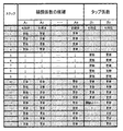
- FIG. 2 is a diagram for explaining an update process for reducing the convergence time.
- the update processing unit 204 first converges by an iterative method only for the compensation coefficient A i (a compensation coefficient selected according to the amplitude of the baseband signal x t among A 1 to A 8 ). The calculation is executed for a predetermined time, and the compensation coefficient A i is sequentially updated (steps 0 to 4 in FIG. 2). During this time, the values of tap coefficients B 1 and B 2 are set to constant values (initial values).
- the update processing unit 204 executes convergence calculation by the iterative method only for the tap coefficients B 1 and B 2 for a predetermined time, and sequentially updates the tap coefficients B 1 and B 2 (Steps 5 to 5 in FIG. 2). 9).
- the value of the compensation coefficient A i is set to a constant value (the value last updated in step 4 in FIG. 2).
- the update processing unit 204 the compensation coefficient A i, and applies the iterative method for both the tap coefficients B 1, B 2, compensation coefficients A i, and, both of the tap coefficients B 1, B 2 Update sequentially (steps 10 to 18 in FIG. 2).
- the update processing unit 204 considers that the coefficient is 0, and the absolute value of the convergence value becomes smaller than the predetermined threshold.
- the compensation coefficient or tap coefficient is excluded from the target of the convergence calculation.
- B k 0 is set.
- the absolute value of the converged value of the tap coefficient B 1 at step 14 is shown an example of when it becomes smaller than a predetermined threshold value.
- the distortion compensation device and the distortion compensation method according to the present invention are suitable for use in a distortion compensation device and a distortion compensation method for compensating for distortion of an output signal output from a predetermined circuit.
Abstract
Disclosed is a distortion-compensation device that can both perform distortion compensation with high precision and reduce the amount of storage space taken up by coefficients required for distortion-compensation calculations. Said distortion-compensation device (100) uses predistortion, in which an input signal is premultiplied by coefficients, to compensate for distortion in an output signal outputted from a given circuit. A first multiplication unit (200c) in this distortion-compensation device (100) multiplies an input signal by compensation coefficients selected from among candidate compensation coefficients in accordance with the input signal. Second multiplication units (201c1 through 201cm) multiply a delayed version of the input signal by tap coefficients, and an addition unit (202) outputs, to a given circuit, a signal obtained by adding together the compensation-coefficient-multiplied input signal and the tap-coefficient-multiplied delayed input signal.
Description
本発明は、所定の回路から出力される出力信号の歪みを補償する歪み補償装置及び歪み補償方法に関する。
The present invention relates to a distortion compensation apparatus and a distortion compensation method for compensating for distortion of an output signal output from a predetermined circuit.
従来、無線通信機等の送信システムを構成するアナログ回路やRF(Radio Frequency)回路などでは非線形の信号歪みが生じることが知られている。そして、このような信号歪みを補償するため、適応的デジタルプリディストーションと呼ばれる技術が開発されている。
Conventionally, it is known that nonlinear signal distortion occurs in an analog circuit or an RF (Radio Frequency) circuit that constitutes a transmission system such as a wireless communication device. In order to compensate for such signal distortion, a technique called adaptive digital predistortion has been developed.
この技術では、アナログ回路やRF回路の逆特性が、入力信号の振幅やパワーに応じて補償係数としてLUT(Look Up Table)に格納される。そして、入力信号の振幅やパワーに応じた補償係数を入力信号に予め適用することにより歪み補償が実現される。
In this technology, the inverse characteristics of analog circuits and RF circuits are stored in a LUT (Look Up Table) as compensation coefficients according to the amplitude and power of the input signal. And distortion compensation is implement | achieved by previously applying the compensation coefficient according to the amplitude and power of an input signal to an input signal.
また、この技術では、補償係数が適用された入力信号と送信信号とが比較され、その差が小さくなるように適応的に補償係数が更新される。これにより、温度変化や電圧変化の影響で歪み特性が変化した場合でも、信号歪みの補償が効果的になされ得る。
In this technique, the input signal to which the compensation coefficient is applied is compared with the transmission signal, and the compensation coefficient is adaptively updated so that the difference is reduced. Thereby, even when the distortion characteristic changes due to the influence of temperature change or voltage change, the signal distortion can be effectively compensated.
例えば、特許文献1には、増幅器により生じる信号歪みを補償するため、増幅器の入力信号と出力信号との差に基づいて、信号歪みを補償するための補償係数を適応型アルゴリズムにより生成する技術が開示されている。
For example, Patent Document 1 discloses a technique for generating a compensation coefficient for compensating for signal distortion by an adaptive algorithm based on a difference between an input signal and an output signal of the amplifier in order to compensate for signal distortion caused by the amplifier. It is disclosed.
なお、信号歪みにはメモリ効果があることが知られている。メモリ効果とは、信号歪みが現在の入力信号だけでなく、過去の入力信号にも依存するという現象である。しかし、特許文献1の技術では、メモリ効果について何ら考慮されていないので、信号歪みの抑制効果が十分に得られないという問題がある。
Note that signal distortion is known to have a memory effect. The memory effect is a phenomenon in which the signal distortion depends not only on the current input signal but also on the past input signal. However, the technique of Patent Document 1 does not consider the memory effect at all, so that there is a problem that a signal distortion suppression effect cannot be obtained sufficiently.
このような問題を解決するものとして、特許文献2には、現在の入力信号の電力(または振幅)が取り得るL個の状態、および、過去の入力信号の電力(または振幅)が取り得るM個の状態に対応するL×M個の補償係数の候補を予めメモリに記憶しておき、その中から現在および過去の入力信号の電力(または振幅)に応じた補償係数を1つ読み出し、その補償係数を入力信号に適用する技術が開示されている。
In order to solve such a problem, Patent Document 2 discloses L states that can be taken by the power (or amplitude) of the current input signal and M that can be taken by the power (or amplitude) of the past input signal. L × M compensation coefficient candidates corresponding to each state are stored in advance in the memory, and one compensation coefficient corresponding to the power (or amplitude) of the current and past input signals is read out from the candidates, A technique for applying a compensation coefficient to an input signal is disclosed.
しかしながら、上述した特許文献2の技術では、L×M個の補償係数の候補をメモリに記憶しておく必要があるので、必要な記憶容量が大きくなるという問題がある。メモリ効果の影響をより精度よく評価するため、さらに過去の入力信号(状態数N)を考慮することとすれば、補償係数の候補の数はL×M×N個となり、補償係数の記憶に必要な記憶容量が著しく増大する。
However, the technique of Patent Document 2 described above has a problem in that the required storage capacity increases because it is necessary to store L × M compensation coefficient candidates in the memory. In order to evaluate the influence of the memory effect more accurately, if the past input signal (number of states N) is further taken into consideration, the number of compensation coefficient candidates is L × M × N. The required storage capacity increases significantly.
また、特許文献2の技術では、現在の入力信号に対し、1つの補償係数を乗算するだけで歪み補償を行っているが、このような方法では、歪み補償を精度よく行うことが難しいという問題もある。
In the technique of Patent Document 2, distortion compensation is performed by multiplying the current input signal by one compensation coefficient. However, with such a method, it is difficult to perform distortion compensation with high accuracy. There is also.
本発明の目的は、歪み補償を行うための計算に必要な係数を記憶する記憶容量を低減するとともに、歪み補償を精度よく実行することができる歪み補償装置および歪み補償方法を提供することである。
An object of the present invention is to provide a distortion compensation device and a distortion compensation method capable of reducing a storage capacity for storing a coefficient necessary for calculation for performing distortion compensation and accurately executing distortion compensation. .
本発明の歪み補償装置は、入力信号に係数を予め乗算するプリディストーションにより、所定の回路から出力される出力信号の歪みを補償する歪み補償装置であって、第1の係数の候補のうち、前記入力信号に応じて選択された第1の係数と前記入力信号との乗算を行う第1の乗算部と、第2の係数と前記入力信号の遅延信号との乗算を行う第2の乗算部と、前記第1の係数が乗算された入力信号と、前記第2の係数が乗算された遅延信号を加算した信号を前記所定の回路に出力する加算部と、を具備する構成を採る。
The distortion compensation apparatus of the present invention is a distortion compensation apparatus that compensates for distortion of an output signal output from a predetermined circuit by predistortion of multiplying an input signal by a coefficient in advance, and among the first coefficient candidates, A first multiplier for multiplying the input signal by the first coefficient selected according to the input signal; and a second multiplier for multiplying the second coefficient by the delayed signal of the input signal. And an adding unit that outputs an input signal multiplied by the first coefficient and a signal obtained by adding the delayed signal multiplied by the second coefficient to the predetermined circuit.
本発明の歪み補償方法は、入力信号に係数を予め乗算するプリディストーションにより、所定の回路から出力される出力信号の歪みを補償する歪み補償方法であって、第1の係数の候補のうち、前記入力信号に応じて選択された第1の係数と前記入力信号との乗算を行うステップと、第2の係数と前記入力信号の遅延信号との乗算を行うステップと、前記第1の係数が乗算された入力信号と、前記第2の係数が乗算された遅延信号を加算した信号を前記所定の回路に出力するステップと、を具備する。
A distortion compensation method of the present invention is a distortion compensation method for compensating for distortion of an output signal output from a predetermined circuit by predistortion of multiplying an input signal by a coefficient in advance, and among the first coefficient candidates, A step of multiplying the input signal by the first coefficient selected according to the input signal; a step of multiplying the second coefficient by the delayed signal of the input signal; and the first coefficient Outputting a signal obtained by adding the multiplied input signal and the delayed signal multiplied by the second coefficient to the predetermined circuit.
本発明によれば、歪み補償を行うための計算に必要な係数を記憶する記憶容量を低減するとともに、歪み補償を精度よく実行することができる。
According to the present invention, it is possible to reduce the storage capacity for storing the coefficients necessary for the calculation for performing the distortion compensation and execute the distortion compensation with high accuracy.
以下、本発明の実施の形態について、図面を参照して詳細に説明する。
Hereinafter, embodiments of the present invention will be described in detail with reference to the drawings.
図1は、本発明の実施の形態に係る送信装置100の構成を示すブロック図である。この送信装置100は、歪み補償部101、RF(Radio Frequency)変調部102、アンテナ103、フィードバック復調部104を備える。
FIG. 1 is a block diagram showing a configuration of transmitting apparatus 100 according to the embodiment of the present invention. The transmission apparatus 100 includes a distortion compensation unit 101, an RF (Radio Frequency) modulation unit 102, an antenna 103, and a feedback demodulation unit 104.
歪み補償部101は、RF変調部102において生じる信号歪みを補償する。具体的には、歪み補償部101は、適応的デジタルプリディストーションの技術を用いて上記歪みを補償する。歪み補償部101の詳細については後に詳しく説明する。
The distortion compensation unit 101 compensates for signal distortion generated in the RF modulation unit 102. Specifically, the distortion compensator 101 compensates for the distortion using an adaptive digital predistortion technique. Details of the distortion compensation unit 101 will be described later.
RF変調部102は、歪み補償部101により歪みが補償されたベースバンド信号の変調および増幅を行い、アンテナ103から電波を放射させる。アンテナ103は、RF変調部102から出力された信号を電波として放射する。フィードバック復調部104は、RF変調部102から出力された出力信号を復調し、歪み補償部101に出力する。
The RF modulation unit 102 modulates and amplifies the baseband signal whose distortion is compensated by the distortion compensation unit 101, and radiates radio waves from the antenna 103. The antenna 103 radiates the signal output from the RF modulation unit 102 as a radio wave. The feedback demodulator 104 demodulates the output signal output from the RF modulator 102 and outputs the demodulated signal to the distortion compensator 101.
次に、歪み補償部101の構成について詳しく説明する。歪み補償部101は、メモリレス補償部200、メモリ効果補償部201、加算器202、誤差算出部203、更新処理部204を備える。
Next, the configuration of the distortion compensation unit 101 will be described in detail. The distortion compensation unit 101 includes a memoryless compensation unit 200, a memory effect compensation unit 201, an adder 202, an error calculation unit 203, and an update processing unit 204.
メモリレス補償部200は、入力されたベースバンド信号に対して歪み補償を行う。メモリレス補償部200は、アドレス生成部200a、第1の記憶部200b、乗算器200cを備える。
The memoryless compensation unit 200 performs distortion compensation on the input baseband signal. The memoryless compensation unit 200 includes an address generation unit 200a, a first storage unit 200b, and a multiplier 200c.
アドレス生成部200aは、ベースバンド信号の振幅を算出し、算出した振幅に対応するアドレスを生成し、生成したアドレスを第1の記憶部200bに出力する。なお、アドレス生成部200aは、ベースバンド信号の振幅の代わりに、ベースバンド信号のパワーや、振幅の関数、パワーの関数などに応じてアドレスを生成することとしてもよい。
The address generation unit 200a calculates the amplitude of the baseband signal, generates an address corresponding to the calculated amplitude, and outputs the generated address to the first storage unit 200b. Note that the address generation unit 200a may generate an address according to the power of the baseband signal, a function of amplitude, a function of power, or the like instead of the amplitude of the baseband signal.
第1の記憶部200bは、メモリなどの記憶デバイスである。第1の記憶部200bは、ベースバンド信号に対して乗算される補償係数の候補Ai(i=1~n)を記憶するLUT(Look Up Table)として構成される。
The first storage unit 200b is a storage device such as a memory. The first storage unit 200b is configured as an LUT (Look Up Table) that stores compensation coefficient candidates A i (i = 1 to n) to be multiplied with the baseband signal.
そして、第1の記憶部200bは、記憶した補償係数の候補のうち、アドレス生成部200aにより生成されたアドレスに対応する補償係数を乗算器200c、および、更新処理部204に出力する。
Then, the first storage unit 200b outputs the compensation coefficient corresponding to the address generated by the address generation unit 200a among the stored compensation coefficient candidates to the multiplier 200c and the update processing unit 204.
乗算器200cは、第1の記憶部200bにより出力された補償係数とベースバンド信号との乗算を行い、その結果得られた信号を加算器202に出力する。
Multiplier 200c multiplies the compensation coefficient output from first storage unit 200b by the baseband signal, and outputs the resulting signal to adder 202.
メモリ効果補償部201は、ベースバンド信号の遅延信号に対して、メモリ効果を補償するための信号処理を行う。メモリ効果補償部201は、遅延器201a1~201am、第2の記憶部201b、乗算器201c1~201cmを備える。
The memory effect compensation unit 201 performs signal processing for compensating for the memory effect on the delayed signal of the baseband signal. Memory effect compensation unit 201 includes delay units 201a 1 ~ 201a m, the second storage section 201b, a multiplier 201c 1 ~ 201c m.
遅延器201a1~201amは、過去(1次、2次、・・・、m次遅れ)のベースバンド信号を保持する。本実施の形態では、遅延器201a1~201amがm個あることとしたが、遅延器201a1~201amの数は少なくとも1つ以上あればよい。
The delay devices 201a 1 to 201a m hold the past (first order, second order,..., Mth order delay) baseband signals. In the present embodiment, there are m delay units 201a 1 to 201a m, but the number of delay units 201a 1 to 201a m may be at least one.
第2の記憶部201bは、メモリなどの記憶デバイスである。第2の記憶部201bは、ベースバンド信号の遅延信号に対して乗算されるタップ係数Bj(j=1~m)を記憶するLUT(Look Up Table)として構成される。第2の記憶部201bは、記憶したタップ係数を乗算器201c1~201cm、および、更新処理部204に出力する。
The second storage unit 201b is a storage device such as a memory. The second storage unit 201b is configured as an LUT (Look Up Table) that stores tap coefficients B j (j = 1 to m) to be multiplied with the delayed signal of the baseband signal. The second storage unit 201b outputs the stored tap coefficient multipliers 201c 1 ~ 201c m, and the update processing unit 204.
乗算器201c1~201cmは、第2の記憶部201bにより出力されたタップ係数とベースバンド信号の遅延信号との乗算を行い、その結果得られた信号を加算器202に出力する。
Multipliers 201c 1 ~ 201c m performs multiplication of delayed signal to the second tap coefficients and the baseband signal output by the storage unit 201b, and outputs the resulting signal to the adder 202.
加算器202は、メモリレス補償部200の乗算器200cにより出力された信号と、メモリ効果補償部201の乗算器201c1~201cmにより出力された信号の和を算出し、その結果得られた信号をRF変調部102に出力する。
Adder 202, a signal output by the multiplier 200c of the memoryless compensator 200 calculates the sum of the multipliers 201c 1 ~ 201c the signal output by the m memory effect compensation unit 201, the resulting The signal is output to the RF modulation unit 102.
誤差算出部203は、時刻tにおいて入力されたベースバンド信号xtと、フィードバック復調部104において出力信号が復調された結果得られた信号ytとの差et(=xt-yt)を算出し、その差の情報を更新処理部204に出力する。この差の絶対値が小さいほど、歪み補償が有効になされているといえる。
The error calculation unit 203 determines the difference e t (= x t −y t ) between the baseband signal x t input at time t and the signal y t obtained as a result of demodulating the output signal in the feedback demodulation unit 104. And the difference information is output to the update processing unit 204. It can be said that the smaller the absolute value of this difference, the more effective the distortion compensation.
更新処理部204は、誤差算出部203により出力された差etの情報を用いて、第1の記憶部200bに記憶された補償係数Ai(i=1~n)、および、第2の記憶部201bに記憶されたタップ係数Bj(j=1~m)を更新する。
Update processing unit 204 uses the output information of the difference e t by the error calculating unit 203, the first storage unit 200b in the stored compensation coefficient A i (i = 1 ~ n ), and, in the second The tap coefficient B j (j = 1 to m) stored in the storage unit 201b is updated.
具体的には、時刻t-jにおけるベースバンド信号をxt-jとすると、フィードバック復調部104において出力信号が復調された結果得られる信号ytは、
yt=(Aixt+ΣAiBjxt-j)f
と表される。ここで、Aiは、第1の記憶部200bに記憶されている補償係数の候補の中から、ベースバンド信号xtの振幅に応じて選択された補償係数、fは、RF変調部102において生じる歪みの影響を表す関数である。 Specifically, assuming that the baseband signal at time t−j is x t−j , the signal y t obtained as a result of demodulating the output signal in thefeedback demodulator 104 is
y t = (A i x t + ΣA i B j x t−j ) f
It is expressed. Here, A i from among the candidates of the compensation coefficients stored in thefirst storage unit 200b, the compensation coefficient selected in accordance with the amplitude of the baseband signal x t, f, in the RF modulation unit 102 It is a function that represents the effect of distortion that occurs.
yt=(Aixt+ΣAiBjxt-j)f
と表される。ここで、Aiは、第1の記憶部200bに記憶されている補償係数の候補の中から、ベースバンド信号xtの振幅に応じて選択された補償係数、fは、RF変調部102において生じる歪みの影響を表す関数である。 Specifically, assuming that the baseband signal at time t−j is x t−j , the signal y t obtained as a result of demodulating the output signal in the
y t = (A i x t + ΣA i B j x t−j ) f
It is expressed. Here, A i from among the candidates of the compensation coefficients stored in the
更新処理部204は、広く普及しているLMS(Least Mean Square)やRLS(Recursive Least Square Algorithm)などの反復法による収束計算を行って、入力されたベースバンド信号xtと、フィードバック復調部104による復調の結果得られた信号ytとの差et、すなわち、
et=xt-yt=xt-(Aixt+ΣAiBjxt-j)f
の絶対値が小さくなるよう、補償係数Ai、および、各タップ係数Bj(j=1~m)の値を決定する。 Theupdate processing unit 204 performs convergence calculation by an iterative method such as LMS (Least Mean Square) and RLS (Recursive Least Square Algorithm), which are widely used, and the input baseband signal x t and the feedback demodulation unit 104. The difference e t from the signal y t obtained as a result of demodulation by
e t = x t −y t = x t − (A i x t + ΣA i B j x t−j ) f
The values of the compensation coefficient A i and each tap coefficient B j (j = 1 to m) are determined so that the absolute value of becomes small.
et=xt-yt=xt-(Aixt+ΣAiBjxt-j)f
の絶対値が小さくなるよう、補償係数Ai、および、各タップ係数Bj(j=1~m)の値を決定する。 The
e t = x t −y t = x t − (A i x t + ΣA i B j x t−j ) f
The values of the compensation coefficient A i and each tap coefficient B j (j = 1 to m) are determined so that the absolute value of becomes small.
そして、更新処理部204は、決定したそれぞれの値で第1の記憶部200bに記憶されている補償係数Ai、および、第2の記憶部201bに記憶されている各タップ係数Bj(j=1~m)の値を更新する。
Then, the update processing unit 204 uses the determined values to store the compensation coefficient A i stored in the first storage unit 200b and the tap coefficients B j (j stored in the second storage unit 201b. = 1 to m) is updated.
このように、本実施の形態では、過去の各ベースバンド信号に対してタップ係数を1つずつ記憶しておけばよいため、歪み補償に必要な記憶容量を低減することができる。また、現在のベースバンド信号に補償係数を乗算して信号を生成するだけでなく、過去のベースバンド信号にタップ係数を乗算して信号を生成し、それらの信号を合成して歪み補正を行うため、精度よい歪み補償が可能となる。
As described above, in this embodiment, since it is only necessary to store one tap coefficient for each past baseband signal, the storage capacity necessary for distortion compensation can be reduced. In addition to generating a signal by multiplying the current baseband signal by a compensation coefficient, a signal is generated by multiplying a past baseband signal by a tap coefficient, and these signals are combined to perform distortion correction. Therefore, accurate distortion compensation is possible.
さらに、次のような更新処理を行うことにより、補償係数Ai、および、各タップ係数Bj(j=1~m)の収束に要する時間を低減させることもできる。図2は、収束時間を低減させる更新処理について説明する図である。なお、図2には、補償係数の候補の数が8(n=8)で、タップ係数の数が2(m=2)である場合について示してある。
Furthermore, the time required for convergence of the compensation coefficient A i and each tap coefficient B j (j = 1 to m) can be reduced by performing the following update process. FIG. 2 is a diagram for explaining an update process for reducing the convergence time. FIG. 2 shows a case where the number of compensation coefficient candidates is 8 (n = 8) and the number of tap coefficients is 2 (m = 2).
この更新処理では、更新処理部204は、まず、補償係数Ai(A1~A8のうち、ベースバンド信号xtの振幅に応じて選択された補償係数)に対してのみ反復法による収束計算を所定の時間実行し、補償係数Aiを順次更新する(図2のステップ0~4)。この間、タップ係数B1、B2の値については、一定の値(初期値)に設定される。
In this update process, the update processing unit 204 first converges by an iterative method only for the compensation coefficient A i (a compensation coefficient selected according to the amplitude of the baseband signal x t among A 1 to A 8 ). The calculation is executed for a predetermined time, and the compensation coefficient A i is sequentially updated (steps 0 to 4 in FIG. 2). During this time, the values of tap coefficients B 1 and B 2 are set to constant values (initial values).
続いて、更新処理部204は、タップ係数B1、B2に対してのみ反復法による収束計算を所定の時間実行し、タップ係数B1、B2を順次更新する(図2のステップ5~9)。この間、補償係数Aiの値については、一定の値(図2のステップ4で最後に更新された値)に設定される。
Subsequently, the update processing unit 204 executes convergence calculation by the iterative method only for the tap coefficients B 1 and B 2 for a predetermined time, and sequentially updates the tap coefficients B 1 and B 2 (Steps 5 to 5 in FIG. 2). 9). During this time, the value of the compensation coefficient A i is set to a constant value (the value last updated in step 4 in FIG. 2).
その後、更新処理部204は、補償係数Ai、および、タップ係数B1、B2の両方に対して反復法を適用し、補償係数Ai、および、タップ係数B1、B2の両方を順次更新する(図2のステップ10~18)。
Thereafter, the update processing unit 204, the compensation coefficient A i, and applies the iterative method for both the tap coefficients B 1, B 2, compensation coefficients A i, and, both of the tap coefficients B 1, B 2 Update sequentially (steps 10 to 18 in FIG. 2).
このような処理により、初めから補償係数Ai、および、タップ係数B1、B2の両方を同時に収束させる場合と比較して、より短時間で補償係数Ai、および、タップ係数B1、B2を収束させることができる。
By such processing, the compensation from the beginning coefficients A i, and, as compared with the case to converge both tap coefficients B 1, B 2 simultaneously, shorter time compensation coefficients A i, and the tap coefficients B 1, B 2 can be converged.
また、更新処理部204は、タップ係数の収束値の絶対値が所定の閾値よりも小さくなった場合、その係数が0であるとみなし、収束値の絶対値が所定の閾値よりも小さくなった補償係数、または、タップ係数を収束計算の対象から除外する。
In addition, when the absolute value of the convergence value of the tap coefficient becomes smaller than a predetermined threshold, the update processing unit 204 considers that the coefficient is 0, and the absolute value of the convergence value becomes smaller than the predetermined threshold. The compensation coefficient or tap coefficient is excluded from the target of the convergence calculation.
また、タップ係数Bkの収束値の絶対値が所定の閾値よりも小さくなった場合は、Bk=0として、
et=xt-yt=xt-(Aixt+Σj≠kAiBjxt-j)f
の絶対値が小さくなるよう、補償係数Ai、および、タップ係数Bj(j=1~m、j≠k)の値を決定する。 Further, when the absolute value of the convergence value of the tap coefficient B k is smaller than a predetermined threshold, B k = 0 is set.
e t = x t −y t = x t − (A i x t + Σ j ≠ k A i B j x t−j ) f
The values of the compensation coefficient A i and the tap coefficient B j (j = 1 to m, j ≠ k) are determined so that the absolute value of becomes small.
図2には、ステップ14でタップ係数B1の収束値の絶対値が所定の閾値よりも小さくなった場合の例が示されている。このような処理により、各係数をより速く収束させることができ、またこの場合B1の更新処理に関する回路は停止させることができるため、省電力化を図ることも可能となる。
2, the absolute value of the converged value of the tap coefficient B 1 at step 14 is shown an example of when it becomes smaller than a predetermined threshold value. By such processing, each coefficient can be converged faster, also circuits related to the updating process in this case B 1 represents because it can be stopped, it is also possible to achieve power saving.
なお、上記実施の形態では、更新処理部204が、誤差算出部203により出力された差etの情報を用いて、補償係数Ai、および、タップ係数Bj(j=1~m)を更新することとしたが、各係数の一部(例えば、補償係数の候補もしくはタップ係数)または全部を予め実験等で求めた値に設定し、更新処理部204による更新を行わないようにしてもよい。
In the above embodiment, the update processing unit 204, using the output information of the difference e t by the error calculating section 203, compensation coefficient A i, and the tap coefficient B j (j = 1 ~ m ) Although it is decided to update, some or all of the coefficients (for example, compensation coefficient candidates or tap coefficients) or all of them are set to values obtained in advance through experiments or the like so that the update processing unit 204 does not perform the update. Good.
2012年12月26日出願の特願2012-282752の日本出願に基づく優先権を主張する。本日本出願に含まれる明細書、図面および要約書の開示内容は、すべて本願に援用される。
Claims priority based on Japanese application of Japanese Patent Application No. 2012-282275 filed on Dec. 26, 2012. The disclosures of the specification, drawings and abstract contained in this Japanese application are all incorporated herein.
本発明にかかる歪み補償装置および歪み補償方法は、所定の回路から出力される出力信号の歪みを補償する歪み補償装置および歪み補償方法に用いるのに好適である。
The distortion compensation device and the distortion compensation method according to the present invention are suitable for use in a distortion compensation device and a distortion compensation method for compensating for distortion of an output signal output from a predetermined circuit.
100 送信装置
101 歪み補償部
102 RF変調部
103 アンテナ
104 フィードバック復調部
200 メモリレス補償部
200a アドレス生成部
200b 第1の記憶部
200c 乗算器
201 メモリ効果補償部
201a1~201am 遅延器
201b 第2の記憶部
201c1~201cm 乗算器
202 加算器
203 誤差算出部
204 更新処理部
100transmitter 101 distortion compensator 102 RF modulator 103 antenna 104 feedback demodulator 200 memoryless compensator 200a address generating unit 200b first storage unit 200c multiplier 201 memory effect compensator 201a 1 ~ 201a m delay unit 201b second Storage unit 201c 1 to 201c m multiplier 202 adder 203 error calculation unit 204 update processing unit
101 歪み補償部
102 RF変調部
103 アンテナ
104 フィードバック復調部
200 メモリレス補償部
200a アドレス生成部
200b 第1の記憶部
200c 乗算器
201 メモリ効果補償部
201a1~201am 遅延器
201b 第2の記憶部
201c1~201cm 乗算器
202 加算器
203 誤差算出部
204 更新処理部
100
Claims (12)
- 入力信号に係数を予め乗算するプリディストーションにより、所定の回路から出力される出力信号の歪みを補償する歪み補償装置であって、
第1の係数の候補のうち、前記入力信号に応じて選択された第1の係数と前記入力信号との乗算を行う第1の乗算部と、
第2の係数と前記入力信号の遅延信号との乗算を行う第2の乗算部と、
前記第1の係数が乗算された入力信号と、前記第2の係数が乗算された遅延信号を加算した信号を前記所定の回路に出力する加算部と、
を具備する歪み補償装置。 A distortion compensation device that compensates for distortion of an output signal output from a predetermined circuit by predistortion of multiplying an input signal by a coefficient,
A first multiplier for multiplying the input signal by the first coefficient selected according to the input signal among the candidates for the first coefficient;
A second multiplier that multiplies the second coefficient by the delayed signal of the input signal;
An adder that outputs a signal obtained by adding the input signal multiplied by the first coefficient and the delayed signal multiplied by the second coefficient to the predetermined circuit;
A distortion compensation apparatus comprising: - 前記出力信号と前記入力信号とに基づいて、前記第2の係数の更新処理を実行する更新処理部をさらに具備する
請求項1記載の歪み補償装置。 The distortion compensation apparatus according to claim 1, further comprising an update processing unit that executes an update process of the second coefficient based on the output signal and the input signal. - 前記更新処理部は、前記出力信号と前記入力信号とに基づいて、前記第1の係数の更新処理を実行する
請求項2記載の歪み補償装置。 The distortion compensation apparatus according to claim 2, wherein the update processing unit executes update processing of the first coefficient based on the output signal and the input signal. - 前記更新処理部は、反復法を用いた収束計算により前記更新処理を実行する
請求項2記載の歪み補償装置。 The distortion compensation apparatus according to claim 2, wherein the update processing unit executes the update process by convergence calculation using an iterative method. - 前記更新処理部は、反復法を用いた収束計算により前記更新処理を実行する
請求項3記載の歪み補償装置。 The distortion compensation apparatus according to claim 3, wherein the update processing unit executes the update processing by convergence calculation using an iterative method. - 前記出力信号と前記入力信号とに基づいて、前記第1の係数と前記第2の係数の更新処理を、反復法を用いた収束計算により実行する更新処理部をさらに具備し、該更新処理は、まず前記第1の係数に対してのみ前記収束計算を実行し、続いて前記第2の係数に対してのみ前記収束計算を実行し、次に前記第1の係数、および、前記第2の係数の両方に対して前記収束計算を実行することによりなされる
請求項1記載の歪み補償装置。 The update processing unit further executes update processing of the first coefficient and the second coefficient by convergence calculation using an iterative method based on the output signal and the input signal, , First performing the convergence calculation only for the first coefficient, then performing the convergence calculation only for the second coefficient, then the first coefficient, and the second coefficient The distortion compensation apparatus according to claim 1, which is performed by executing the convergence calculation for both coefficients. - 前記更新処理部は、前記第2の係数の更新処理における更新値の絶対値が所定の閾値よりも小さい場合に、該更新値を示す更新対象を前記収束計算の対象から除外する
請求項4記載の歪み補償装置。 The update processing unit excludes an update target indicating the update value from the target of the convergence calculation when the absolute value of the update value in the update processing of the second coefficient is smaller than a predetermined threshold. Distortion compensation device. - 前記更新処理部は、前記第2の係数の更新処理における更新値の絶対値が所定の閾値よりも小さい場合に、該更新値を示す更新対象を前記収束計算の対象から除外する
請求項6記載の歪み補償装置。 The update processing unit excludes an update target indicating the update value from the target of the convergence calculation when the absolute value of the update value in the update processing of the second coefficient is smaller than a predetermined threshold value. Distortion compensation device. - 前記反復法は、Least Mean Square法である
請求項4記載の歪み補償装置。 The distortion compensation apparatus according to claim 4, wherein the iterative method is a Least Mean Square method. - 前記反復法は、Least Mean Square法である
請求項5記載の歪み補償装置。 The distortion compensation apparatus according to claim 5, wherein the iterative method is a Least Mean Square method. - 前記反復法は、Least Mean Square法である
請求項6記載の歪み補償装置。 The distortion compensation apparatus according to claim 6, wherein the iterative method is a Least Mean Square method. - 入力信号に係数を予め乗算するプリディストーションにより、所定の回路から出力される出力信号の歪みを補償する歪み補償方法であって、
第1の係数の候補のうち、前記入力信号に応じて選択された第1の係数と前記入力信号との乗算を行うステップと、
第2の係数と前記入力信号の遅延信号との乗算を行うステップと、
前記第1の係数が乗算された入力信号と、前記第2の係数が乗算された遅延信号を加算した信号を前記所定の回路に出力するステップと、
を具備する歪み補償方法。 A distortion compensation method for compensating for distortion of an output signal output from a predetermined circuit by predistortion of multiplying an input signal by a coefficient,
Multiplying the input signal by the first coefficient selected according to the input signal among the candidates for the first coefficient;
Multiplying a second coefficient by the delayed signal of the input signal;
Outputting a signal obtained by adding the input signal multiplied by the first coefficient and the delayed signal multiplied by the second coefficient to the predetermined circuit;
A distortion compensation method comprising:
Priority Applications (1)
| Application Number | Priority Date | Filing Date | Title |
|---|---|---|---|
| US14/655,217 US9531332B2 (en) | 2012-12-26 | 2013-11-29 | Distortion-compensation device and distortion-compensation method |
Applications Claiming Priority (2)
| Application Number | Priority Date | Filing Date | Title |
|---|---|---|---|
| JP2012-282752 | 2012-12-26 | ||
| JP2012282752A JP6054739B2 (en) | 2012-12-26 | 2012-12-26 | Distortion compensation apparatus and distortion compensation method |
Publications (1)
| Publication Number | Publication Date |
|---|---|
| WO2014103175A1 true WO2014103175A1 (en) | 2014-07-03 |
Family
ID=51020303
Family Applications (1)
| Application Number | Title | Priority Date | Filing Date |
|---|---|---|---|
| PCT/JP2013/007043 WO2014103175A1 (en) | 2012-12-26 | 2013-11-29 | Distortion-compensation device and distortion-compensation method |
Country Status (3)
| Country | Link |
|---|---|
| US (1) | US9531332B2 (en) |
| JP (1) | JP6054739B2 (en) |
| WO (1) | WO2014103175A1 (en) |
Families Citing this family (7)
| Publication number | Priority date | Publication date | Assignee | Title |
|---|---|---|---|---|
| US20180054170A1 (en) * | 2016-08-19 | 2018-02-22 | Fujitsu Limited | Distortion compensation device and coefficient update method |
| US9942074B1 (en) | 2016-11-30 | 2018-04-10 | Micron Technology, Inc. | Wireless devices and systems including examples of mixing coefficient data specific to a processing mode selection |
| US10027523B2 (en) | 2016-11-30 | 2018-07-17 | Micron Technology, Inc. | Wireless devices and systems including examples of mixing input data with coefficient data |
| US11005430B2 (en) | 2017-03-02 | 2021-05-11 | Sumitomo Electric Industries, Ltd. | Distortion compensation device and distortion compensation method |
| EP3804129A1 (en) * | 2018-06-05 | 2021-04-14 | Telefonaktiebolaget LM Ericsson (publ) | Digital predistortion low power implementation |
| US10886998B2 (en) | 2019-02-22 | 2021-01-05 | Micron Technology, Inc. | Mixing coefficient data specific to a processing mode selection using layers of multiplication/accumulation units for wireless communication |
| US10924152B1 (en) | 2019-11-13 | 2021-02-16 | Micron Technology, Inc. | Mixing coefficient data for processing mode selection |
Citations (5)
| Publication number | Priority date | Publication date | Assignee | Title |
|---|---|---|---|---|
| WO2009090825A1 (en) * | 2008-01-15 | 2009-07-23 | Mitsubishi Electric Corporation | Predistorter |
| JP2010518660A (en) * | 2006-12-26 | 2010-05-27 | ダリ システムズ カンパニー リミテッド | Method and system for linearizing baseband predistortion in multi-channel wideband communication system |
| JP2010183525A (en) * | 2009-02-09 | 2010-08-19 | Hitachi Kokusai Electric Inc | Predistorter |
| JP2011135143A (en) * | 2009-12-22 | 2011-07-07 | Hitachi Kokusai Electric Inc | Distortion compensating apparatus of predistortion system |
| JP2011176686A (en) * | 2010-02-25 | 2011-09-08 | Nec Corp | Predistortion compensation circuit and memory effect distortion compensation method for power amplifier |
Family Cites Families (3)
| Publication number | Priority date | Publication date | Assignee | Title |
|---|---|---|---|---|
| JP3560398B2 (en) | 1995-08-31 | 2004-09-02 | 富士通株式会社 | Amplifier with distortion compensation |
| WO2001008320A1 (en) | 1999-07-28 | 2001-02-01 | Fujitsu Limited | Method and apparatus for distortion compensation of radio device |
| EP1914885B1 (en) * | 2005-06-30 | 2012-03-07 | Fujitsu Ltd. | Power amplifier having distortion compensating circuit |
-
2012
- 2012-12-26 JP JP2012282752A patent/JP6054739B2/en not_active Expired - Fee Related
-
2013
- 2013-11-29 WO PCT/JP2013/007043 patent/WO2014103175A1/en active Application Filing
- 2013-11-29 US US14/655,217 patent/US9531332B2/en not_active Expired - Fee Related
Patent Citations (5)
| Publication number | Priority date | Publication date | Assignee | Title |
|---|---|---|---|---|
| JP2010518660A (en) * | 2006-12-26 | 2010-05-27 | ダリ システムズ カンパニー リミテッド | Method and system for linearizing baseband predistortion in multi-channel wideband communication system |
| WO2009090825A1 (en) * | 2008-01-15 | 2009-07-23 | Mitsubishi Electric Corporation | Predistorter |
| JP2010183525A (en) * | 2009-02-09 | 2010-08-19 | Hitachi Kokusai Electric Inc | Predistorter |
| JP2011135143A (en) * | 2009-12-22 | 2011-07-07 | Hitachi Kokusai Electric Inc | Distortion compensating apparatus of predistortion system |
| JP2011176686A (en) * | 2010-02-25 | 2011-09-08 | Nec Corp | Predistortion compensation circuit and memory effect distortion compensation method for power amplifier |
Also Published As
| Publication number | Publication date |
|---|---|
| US20150349725A1 (en) | 2015-12-03 |
| JP2014127829A (en) | 2014-07-07 |
| JP6054739B2 (en) | 2016-12-27 |
| US9531332B2 (en) | 2016-12-27 |
Similar Documents
| Publication | Publication Date | Title |
|---|---|---|
| WO2014103175A1 (en) | Distortion-compensation device and distortion-compensation method | |
| US8737937B2 (en) | Distortion compensation apparatus, transmitter, and distortion compensation method | |
| US8933752B2 (en) | Power amplifier apparatus, distortion compensation coefficient updating method, and transmission apparatus | |
| US20070296495A1 (en) | Distortion compensating apparatus | |
| JP2006279780A (en) | Distortion compensation apparatus and distortion correction method | |
| US10797737B2 (en) | Distortion compensation device and distortion compensation method | |
| US20150214904A1 (en) | Distortion compensation apparatus and distortion compensation method | |
| US9450544B2 (en) | Pre-distortion method, associated apparatus and non-transitory machine readable medium | |
| US20090227216A1 (en) | Apparatus for updating coefficient for distortion compensation and amplifier for compensating distortion | |
| US9853664B2 (en) | Radio frequency power amplification system, radio frequency power amplification method, transmitter, and base station | |
| JP5124655B2 (en) | Distortion compensation amplifier | |
| JP5707999B2 (en) | Distortion compensation apparatus, transmitter, and distortion compensation method | |
| US20180013456A1 (en) | Distortion compensation device and distortion compensation method | |
| US9438177B2 (en) | Pre-distortion method and associated apparatus and non-transitory machine readable medium | |
| US9548703B2 (en) | Distortion compensation apparatus, transmission apparatus, and distortion compensation method | |
| JP5299958B2 (en) | Predistorter | |
| JP5387445B2 (en) | Predistortion compensation circuit and memory effect distortion compensation method for power amplifier | |
| US9680511B1 (en) | Distortion compensator, distortion compensation method and radio equipment | |
| JP2006295440A (en) | Distortion compensation device and delay amount control method | |
| KR100939882B1 (en) | Strain compensation device | |
| JP2015023507A (en) | Distortion compensation device | |
| US9768891B2 (en) | Distortion compensation device and distortion compensation method | |
| JP2008236592A (en) | Receiver and radio apparatus | |
| JP2005079935A (en) | Adaptive predistortion type distortion compensation power amplifier | |
| JP2014168114A (en) | Distortion compensation device and distortion compensation method |
Legal Events
| Date | Code | Title | Description |
|---|---|---|---|
| 121 | Ep: the epo has been informed by wipo that ep was designated in this application |
Ref document number: 13868573 Country of ref document: EP Kind code of ref document: A1 |
|
| WWE | Wipo information: entry into national phase |
Ref document number: 14655217 Country of ref document: US |
|
| NENP | Non-entry into the national phase |
Ref country code: DE |
|
| 122 | Ep: pct application non-entry in european phase |
Ref document number: 13868573 Country of ref document: EP Kind code of ref document: A1 |