WO2014091934A1 - 通信装置、通信方法、集積回路、及び、電子機器 - Google Patents
通信装置、通信方法、集積回路、及び、電子機器 Download PDFInfo
- Publication number
- WO2014091934A1 WO2014091934A1 PCT/JP2013/082014 JP2013082014W WO2014091934A1 WO 2014091934 A1 WO2014091934 A1 WO 2014091934A1 JP 2013082014 W JP2013082014 W JP 2013082014W WO 2014091934 A1 WO2014091934 A1 WO 2014091934A1
- Authority
- WO
- WIPO (PCT)
- Prior art keywords
- circuit
- communication
- antenna
- transmission data
- writer
- Prior art date
Links
- 238000004891 communication Methods 0.000 title claims abstract description 289
- 238000000034 method Methods 0.000 title claims abstract description 47
- 230000005540 biological transmission Effects 0.000 claims abstract description 201
- 230000005674 electromagnetic induction Effects 0.000 claims description 6
- 238000005516 engineering process Methods 0.000 abstract description 25
- 230000006870 function Effects 0.000 abstract description 22
- 238000004519 manufacturing process Methods 0.000 abstract description 7
- 230000010355 oscillation Effects 0.000 description 36
- 239000003990 capacitor Substances 0.000 description 20
- 239000013078 crystal Substances 0.000 description 10
- 238000010586 diagram Methods 0.000 description 8
- 230000008859 change Effects 0.000 description 6
- 238000000605 extraction Methods 0.000 description 5
- 239000000969 carrier Substances 0.000 description 4
- 230000000694 effects Effects 0.000 description 2
- 230000008569 process Effects 0.000 description 2
- 230000004044 response Effects 0.000 description 2
- 230000007704 transition Effects 0.000 description 2
- 238000010168 coupling process Methods 0.000 description 1
- 239000000284 extract Substances 0.000 description 1
- 239000004973 liquid crystal related substance Substances 0.000 description 1
- 239000000203 mixture Substances 0.000 description 1
- 238000010295 mobile communication Methods 0.000 description 1
- 238000012986 modification Methods 0.000 description 1
- 230000004048 modification Effects 0.000 description 1
- 238000004088 simulation Methods 0.000 description 1
- 239000000758 substrate Substances 0.000 description 1
Images


Classifications
-
- H04B5/77—
-
- G—PHYSICS
- G06—COMPUTING; CALCULATING OR COUNTING
- G06K—GRAPHICAL DATA READING; PRESENTATION OF DATA; RECORD CARRIERS; HANDLING RECORD CARRIERS
- G06K7/00—Methods or arrangements for sensing record carriers, e.g. for reading patterns
- G06K7/10—Methods or arrangements for sensing record carriers, e.g. for reading patterns by electromagnetic radiation, e.g. optical sensing; by corpuscular radiation
- G06K7/10009—Methods or arrangements for sensing record carriers, e.g. for reading patterns by electromagnetic radiation, e.g. optical sensing; by corpuscular radiation sensing by radiation using wavelengths larger than 0.1 mm, e.g. radio-waves or microwaves
- G06K7/10297—Methods or arrangements for sensing record carriers, e.g. for reading patterns by electromagnetic radiation, e.g. optical sensing; by corpuscular radiation sensing by radiation using wavelengths larger than 0.1 mm, e.g. radio-waves or microwaves arrangements for handling protocols designed for non-contact record carriers such as RFIDs NFCs, e.g. ISO/IEC 14443 and 18092
-
- G—PHYSICS
- G06—COMPUTING; CALCULATING OR COUNTING
- G06K—GRAPHICAL DATA READING; PRESENTATION OF DATA; RECORD CARRIERS; HANDLING RECORD CARRIERS
- G06K7/00—Methods or arrangements for sensing record carriers, e.g. for reading patterns
- G06K7/10—Methods or arrangements for sensing record carriers, e.g. for reading patterns by electromagnetic radiation, e.g. optical sensing; by corpuscular radiation
- G06K7/10009—Methods or arrangements for sensing record carriers, e.g. for reading patterns by electromagnetic radiation, e.g. optical sensing; by corpuscular radiation sensing by radiation using wavelengths larger than 0.1 mm, e.g. radio-waves or microwaves
- G06K7/10366—Methods or arrangements for sensing record carriers, e.g. for reading patterns by electromagnetic radiation, e.g. optical sensing; by corpuscular radiation sensing by radiation using wavelengths larger than 0.1 mm, e.g. radio-waves or microwaves the interrogation device being adapted for miscellaneous applications
-
- H04B5/26—
Definitions
- the present technology relates to a communication device, a communication method, an integrated circuit, and an electronic device, and more particularly, to a communication device, a communication method, an integrated circuit, and an electronic device that can reduce manufacturing costs.
- RFID Radio Frequency IDentification
- some RF tags have a function as a reader / writer that communicates with other RF tags in addition to a function as an RF tag that communicates with a dedicated reader / writer.
- Such an RF tag operates as an RF tag or a reader / writer depending on the usage state.
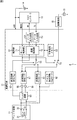
- FIG. 1 shows a configuration of a communication device 1 in which both functions of an RF tag and a reader / writer are mounted.
- the communication device 1 includes an antenna circuit 11, an integrated circuit 12, a host controller 13, a power source 14, an oscillation circuit 15, and a crystal oscillator 16.
- the antenna circuit 11 includes a coil 31 and a capacitor 32, and forms a parallel resonance circuit.
- the power supply 14 supplies power to the integrated circuit 12 and the host controller 13.
- the oscillation circuit 15 generates a carrier having a frequency (13.56 MHz) corresponding to the vibration frequency of the crystal oscillator 16.
- the integrated circuit 12 modulates transmission data in accordance with control from the host controller 13 and transmits a modulation signal obtained thereby to the communication destination via the antenna circuit 11. Further, the integrated circuit 12 receives a demodulated signal from the communication destination via the antenna circuit 11 and demodulates it according to the control from the host controller 13.
- the integrated circuit 12 includes a control unit 51 that controls each unit, a nonvolatile memory 52 that appropriately stores various data, a data input circuit 53 that inputs transmission data, and a data output circuit 54 that outputs reception data.
- the control unit 51 includes a mode control unit 71 and a communication control unit 72.
- the mode control unit 71 controls the switching operation of the switch 55 and the switch 56 in accordance with the control from the host controller 13.
- the communication control unit 72 controls input / output of transmission data and reception data, and performs various processes on the data.
- the operation mode of the communication device 1 includes a reader / writer mode that operates as a reader / writer and a tag mode that operates as an RF tag. Therefore, the integrated circuit 12 is provided with a transmission circuit 57 as a circuit for a reader / writer function, a transmission circuit 61 as a circuit for an RF tag function, and a reception circuit 63 as a circuit for both of these functions. Is provided.
- the transmission data from the communication control unit 72 is amplitude-shift keyed (ASK: Amplitude Shift Keying, hereinafter referred to as “ASK modulation”) according to the carrier generated by the oscillation circuit 15. ).
- ASK modulation amplitude-shift keyed
- transmission buffer circuits 58 and 59 are provided so that the carrier can be driven with low impedance. Accordingly, the ASK-modulated modulation signal is transmitted to the communication destination RF tag via the filter circuit 60 and the antenna circuit 11.
- the transmission circuit 61 When the transmission circuit 61 operates in the tag mode, the transmission data for reply from the communication control unit 72 is load-modulated according to the clock signal extracted by the clock extraction circuit 62 and applied to the coil 31 of the antenna circuit 11. . Thereby, the return transmission data is transmitted to the reader / writer of the communication destination.
- the receiving circuit 63 is a circuit that is used in both the reader / writer mode and the tag mode. When operating in the tag mode or the reader / writer mode, the receiving circuit 63 receives and demodulates the modulated signal from the communication destination via the antenna circuit 11 and the filter circuit 60, and performs communication control on the received data obtained thereby. To the unit 72.
- the communication device 1 is configured to have both functions of an RF tag and a reader / writer.
- ASK modulation is used when operating as a reader / writer
- load modulation is used when operating as an RF tag. Therefore, the transmitter circuit 57 for the reader / writer function and the RF tag are used. It is necessary to provide the function transmission circuit 61 separately. For this reason, there has been a demand to reduce the manufacturing cost by sharing the transmission circuit provided exclusively for them.
- the present technology has been made in view of such a situation, and can reduce the manufacturing cost of a communication device having both functions of an RF tag and a reader / writer or an electronic device equipped with the communication device. It is.
- a communication apparatus includes an antenna unit, a transmission unit that modulates transmission data and transmits the transmission data to a communication destination via the antenna unit, and the reception data modulated from the communication destination.
- a receiving unit that receives and demodulates the signal via a communication unit, wherein the transmitting unit and the receiving unit operate as a RFID (Radio Frequency Identification) reader / writer and a communication target of the RFID reader / writer
- the transmission unit uses the first carrier generated in the antenna unit and operates in the transmission mode.
- the transmission data is transmitted to the RFID reader / writer by performing load modulation for changing the impedance of the antenna unit according to the transmission data using the second carrier received by the antenna unit.
- a carrier generation unit for generating the first carrier is further provided.
- the carrier generation unit causes the impedance of the antenna unit to have a predetermined value.
- the communication device may be an independent device or an internal block constituting one device.
- the communication method and electronic device according to one aspect of the present technology are a communication method and electronic device corresponding to the communication device according to one aspect of the present technology.
- the integrated circuit modulates transmission data and transmits the transmission data to a communication destination via an external antenna circuit, and modulates reception data from the communication destination via the antenna circuit.
- a receiving circuit for receiving and demodulating wherein the transmitting circuit and the receiving circuit are of a first operation mode that operates as an RFID reader / writer and a second operation mode that operates as a communication target of the RFID reader / writer.
- the antenna circuit uses the first carrier generated in the antenna circuit according to the transmission data.
- load modulation that changes the impedance of the transmission data
- the transmission data is transmitted to the communication target, and is received by the antenna circuit when operating in the second operation mode.
- Using the second carrier was, in response to said transmitted data, by performing load modulation for changing the impedance of the antenna circuit, and transmits the transmission data to the RFID reader-writer.
- the first carrier is generated by an external carrier generation circuit.
- the carrier generation circuit makes the impedance of the antenna circuit have a predetermined value.
- the transmission data and the reception data are encoded by the same encoding method.
- a voltage setting circuit for limiting a power supply voltage generated by electromagnetic induction of the antenna circuit according to the operation mode is further provided.
- the communication method according to one aspect of the present technology is a communication method corresponding to the integrated circuit according to one aspect of the present technology described above.
- the communication device when operating in the first operation mode, the first carrier generated in the antenna unit is used according to transmission data.
- the transmission data is transmitted to the communication target, and operates in the second operation mode, the second carrier received by the antenna unit is used according to the transmission data.
- load modulation for changing the impedance of the antenna unit is performed, and transmission data is transmitted to the RFID reader / writer.
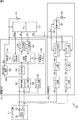
- FIG. 2 is a diagram illustrating a configuration of an embodiment of a communication device to which the present technology is applied.
- the communication device 101 includes an antenna circuit 111, an integrated circuit 112, a host controller 113, a power source 114, and an external circuit 115.
- the antenna circuit 111 has a coil 131 and a capacitor 132, which form a parallel resonant circuit.
- L11 indicates the inductance of the coil 131
- C11 indicates the capacitance of the capacitor 132.
- the antenna circuit 111 is adjusted to an inductor value that can efficiently receive a magnetic field of 13.56 MHz, and the effect can be increased by a variable capacitor.
- the integrated circuit 112 is a circuit having both functions of an RF tag and a reader / writer, and is configured as a so-called IC chip.
- the integrated circuit 112 modulates the input transmission data in accordance with the control from the host controller 113, and transmits the modulated signal obtained thereby to the communication destination via the antenna circuit 111. Further, the integrated circuit 112 receives and demodulates the modulated signal from the communication destination via the antenna circuit 111 according to the control from the host controller 113, and outputs the received data obtained thereby.
- the host controller 113 controls the operation of each unit of the communication device 101. Specifically, the host controller 113 supplies a control signal (MODE) or transmission data (TX) to the integrated circuit 112 and supplies a control signal (EN) to the external circuit 115 according to the operating state of the communication apparatus 101. To do. The host controller 113 acquires the reception data (RX) supplied from the integrated circuit 112 and performs various processes.
- MODE control signal
- TX transmission data
- EN control signal
- the power supply 114 supplies a DC voltage necessary for each circuit to operate as power supply power (VDD) to the integrated circuit 112, the host controller 113, and the external circuit 115.
- VDD power supply power
- the external circuit 115 generates a carrier with a predetermined frequency (13.56 MHz) and applies it to the antenna circuit 111 when the communication apparatus 101 operates in a reader / writer mode, which will be described later, in accordance with control from the host controller 113. To do.
- the antenna circuit 111 always radiates a carrier when operating in the reader / writer mode.
- the integrated circuit 112 includes a control unit 151, a nonvolatile memory 152, a data input circuit 153, a data output circuit 154, a transmission circuit 155, a clock extraction circuit 156, a rectification circuit 157, a reception circuit 158, and a power selection circuit 159.
- the control unit 151 controls the operation of each unit of the integrated circuit 112.
- the nonvolatile memory 152 holds various data according to the control from the control unit 151.
- the data input circuit 153 and the data output circuit 154 are provided for interface with the host controller 113.
- the data input circuit 153 supplies transmission data (TX) from the host controller 113 to the control unit 151. Further, the data output circuit 154 supplies the reception data (RX) from the control unit 151 to the host controller 113.
- control unit 151 is configured to include a mode control unit 171 and a communication control unit 172.
- the mode control unit 171 controls the operation mode of the integrated circuit 112 in accordance with a control signal (MODE) from the host controller 113.
- the operation mode includes a reader / writer mode (first operation mode) in which the communication apparatus 101 operates as a reader / writer, and a tag mode (second operation mode) in which the communication apparatus 101 operates as an RF tag.
- the communication control unit 172 performs transmission control for transmitting transmission data. At this time, the communication control unit 172 encodes the transmission data from the data input circuit 153 by an encoding method called a Manchester method, and then supplies the data to the transmission circuit 155. Further, the communication control unit 172 performs reception control for receiving received data. At this time, the communication control unit 172 decodes the Manchester encoded reception data from the reception circuit 158 and supplies the decoded data to the data output circuit 154. That is, in the near field communication between the communication apparatus 101 and its communication destination, the same encoding method is used when transmitting and receiving data according to a predetermined standard.
- the transmission circuit 155 is a circuit that performs transmission modulation of data used in both the reader / writer mode and the tag mode.
- the transmission circuit 155 uses the carrier generated in the antenna circuit 111 by the external circuit 115 and uses the carrier from the communication control unit 172.
- Load modulation is performed to change the impedance of the parallel resonant circuit of the antenna circuit 111 according to the transmission data.
- the modulated signal from the communication apparatus 101 is transmitted to the communication destination RF tag.
- the antenna circuit 111 When the transmission circuit 155 operates in the tag mode, the antenna circuit 111 receives a carrier from the reader / writer of the communication destination. The transmission circuit 155 uses the received carrier and performs load modulation that changes the impedance of the parallel resonance circuit of the antenna circuit 111 according to the transmission data for return from the communication control unit 172. As a result, the modulation signal from the communication apparatus 101 is transmitted to the reader / writer of the communication destination.
- the clock extraction circuit 156 When operating in the tag mode, the clock extraction circuit 156 extracts a clock signal based on the carrier received from the reader / writer of the communication destination, and supplies it to each part of the integrated circuit 112 such as the transmission circuit 155. Each unit of the integrated circuit 112 performs various operations in accordance with the clock signal extracted by the clock extraction circuit 156.
- the rectifier circuit 157 converts the AC reception voltage generated in the antenna circuit 111 by the reader / writer of the communication destination into a DC voltage, and supplies the DC voltage to the reception circuit 158 and the power selection circuit 159.
- the receiving circuit 158 is a circuit for receiving and demodulating data used in both the reader / writer mode and the tag mode.
- the antenna circuit 111 is induced with a modulation signal generated by load modulation by the communication destination RF tag.
- the receiving circuit 158 demodulates the modulation signal generated in the antenna circuit 111 based on the output from the rectifier circuit 157 and supplies the received data obtained thereby to the communication control unit 172.
- the antenna circuit 111 receives a modulated signal modulated by the reader / writer of the communication destination.
- the receiving circuit 158 demodulates the modulated signal received by the antenna circuit 111 based on the output from the rectifier circuit 157 and supplies the received data obtained thereby to the communication control unit 172.
- the power selection circuit 159 is supplied with power supply power (VDD) from the power supply 114 and DC voltage (power supply power: VDDA) from the rectifier circuit 157.
- the power selection circuit 159 selects the power supply power having a higher voltage from among the power supply powers so as to be supplied to each part of the integrated circuit 112.
- the external circuit 115 includes an oscillation circuit 191, a crystal oscillator 192, a switch 193, a tristate inverter circuit 194, a filter circuit 195, an impedance circuit 196, a tristate buffer circuit 197, a filter circuit 198, and an impedance circuit 199. Is done.
- the oscillation circuit 191 generates an oscillation signal corresponding to the oscillation frequency of the crystal oscillator 192 and supplies the oscillation signal to the tristate inverter circuit 194 and the tristate buffer circuit 197.
- the switch 193 has one terminal connected to the oscillation circuit 191 and the other terminal connected to the power source 114.
- the switch 193 controls the power supply power (VDD) supplied to the oscillation circuit 191 by performing a switching operation in accordance with a control signal (EN) from the host controller 113.
- the tristate inverter circuit 194 changes its output state in accordance with a control signal (EN) from the host controller 113. In the normal output state, the tri-state inverter circuit 194 inverts the oscillation signal from the oscillation circuit 191 and supplies the inverted signal to the filter circuit 195. Further, the tri-state inverter circuit 194 does not function as an inverter in the high impedance output state, and its output is in the high impedance state. Note that the tri-state inverter circuit 194 operates based on power supply power (VDD) from the power supply 114.
- VDD power supply power
- the filter circuit 195 generates a 13.56 MHz carrier (sine wave) based on the normal output from the tri-state inverter circuit 194 and supplies it to the impedance circuit 196.
- the tristate buffer circuit 197 changes its output state in accordance with a control signal (EN) from the host controller 113.
- the tristate buffer circuit 197 supplies the oscillation signal from the oscillation circuit 191 to the filter circuit 198 in the normal output state. Further, the tri-state buffer circuit 197 does not function as a buffer in the high impedance output state, and its output is in the high impedance state. Note that the tristate buffer circuit 197 operates based on power supply power (VDD) from the power supply 114.
- VDD power supply power
- the filter circuit 198 generates a 13.56 MHz carrier (sine wave) based on the normal output from the tristate buffer circuit 197 and supplies it to the impedance circuit 199.
- the impedance circuit 196 has an output terminal connected to one terminal (the upper terminal in the figure) of the antenna circuit 111, and the impedance circuit 199 has an output terminal that is the other terminal (the lower side in the figure). Terminal).
- the impedance circuit 196 and the impedance circuit 199 allow the impedance of the parallel resonant circuit of the antenna circuit 111 to have a predetermined value. It has been found by detailed simulation conducted by the inventor of the present technology that it is preferable that this impedance has a magnitude of about several hundred to 1 K ⁇ .
- the configuration of the communication device 101 has been described above.
- FIG. 3 is a diagram illustrating a configuration of the transmission circuit 155A including a resistor and a MOS switch. As shown in FIG. 3, the transmission circuit 155A is configured by connecting a resistor 175 and a MOS transistor 177 in series, and connecting a resistor 176 and a MOS transistor 178 in series.
- R11 represents the resistance value of the resistor 175, and R12 represents the resistance value of the resistor 176.
- one terminal is connected to one terminal (the upper terminal in the drawing) of the coil 131 of the antenna circuit 111, and the other terminal is connected to the drain terminal of the MOS transistor 177. Further, in the MOS transistor 177, its drain terminal is connected to the other terminal of the resistor 175, and its source terminal is grounded. Further, a signal indicating “1” or “0” corresponding to the transmission data from the communication control unit 172, that is, a modulation signal is supplied to the gate terminal of the MOS transistor 177. The MOS transistor 177 performs an on / off switching operation according to a modulation signal of “1” or “0”.
- one terminal is connected to the other terminal (the lower terminal in the figure) of the coil 131 of the antenna circuit 111, and the other terminal is connected to the drain terminal of the MOS transistor 178. Further, in the MOS transistor 178, its drain terminal is connected to the other terminal of the resistor 176, and its source terminal is grounded. Further, a modulation signal from the communication control unit 172 is supplied to the gate terminal of the MOS transistor 178. The MOS transistor 178 performs an on / off switching operation according to a modulation signal of “1” or “0”.
- the impedance of the parallel resonant circuit of the antenna circuit 111 changes.
- the carrier generated in the antenna circuit 111 is changed, and load modulation is performed.
- FIG. 4 is a diagram illustrating a configuration of the transmission circuit 155B including a capacitor and a MOS switch. As shown in FIG. 4, the transmission circuit 155B includes a capacitor 179 and a MOS transistor 177 connected in series, and a capacitor 180 and a MOS transistor 178 connected in series. In FIG. 4, C12 indicates the capacity of the capacitor 179, and C13 indicates the capacity of the capacitor 180.
- the MOS transistor 177 basically has the same connection relationship as in FIG. 3, but one terminal of a capacitor 179 is connected to the drain terminal. The other terminal of the capacitor 179 is connected to one terminal (the upper terminal in the drawing) of the coil 131 of the antenna circuit 111.
- the MOS transistor 178 basically has the same connection relationship as that of FIG. 3, but one terminal of the capacitor 180 is connected to the drain terminal thereof. The other terminal of the capacitor 180 is connected to the other terminal (the lower terminal in the figure) of the coil 131 of the antenna circuit 111.
- the MOS transistors 177 and 178 perform a switching operation according to the modulation signal, thereby performing load modulation that changes the impedance of the parallel resonance circuit of the antenna circuit 111.
- FIG. 5 is a diagram illustrating a configuration of a transmission circuit 155C including a diode and a MOS switch. As shown in FIG. 5, the transmission circuit 155C is configured by connecting a diode 181 and a MOS transistor 177 in series, and connecting a diode 182 and a MOS transistor 178 in series.
- the MOS transistor 177 basically has a connection relationship similar to that shown in FIG. 3, but the cathode side of the diode 181 is connected to the drain terminal thereof. The anode side of the diode 181 is connected to one terminal (the upper terminal in the figure) of the coil 131 of the antenna circuit 111. Similarly, the MOS transistor 178 basically has the same connection relationship as in FIG. 3, but the cathode side of the diode 182 is connected to the drain terminal. The anode side of the diode 182 is connected to the other terminal (the lower terminal in the figure) of the coil 131 of the antenna circuit 111.
- the MOS transistors 177 and 178 perform a switching operation according to the modulation signal, thereby performing load modulation that changes the impedance of the parallel resonance circuit of the antenna circuit 111.
- FIG. 6 is a diagram illustrating a configuration of a transmission circuit 155D including a combination of a diode and a resistor and a MOS switch.
- the transmission circuit 155D includes a diode 181, a resistor 175, and a MOS transistor 177 connected in series, and a diode 182, a resistor 176, and a MOS transistor 178 connected in series.
- the resistor 175 and the MOS transistor 177 basically have the same connection relationship as in FIG. 3, but the cathode side of the diode 181 is connected to one terminal of the resistor 175.
- the anode side of the diode 181 is connected to one terminal (the upper terminal in the figure) of the coil 131 of the antenna circuit 111.
- the resistor 176 and the MOS transistor 178 basically have the same connection relationship as in FIG. 3, but the cathode side of the diode 182 is connected to one terminal of the resistor 176.
- the anode side of the diode 182 is connected to the other terminal (the lower terminal in the figure) of the coil 131 of the antenna circuit 111.
- the MOS transistors 177 and 178 perform a switching operation according to the modulation signal, thereby performing load modulation that changes the impedance of the parallel resonance circuit of the antenna circuit 111.
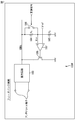
- FIG. 7 is a diagram illustrating a configuration of a transmission circuit 155E that controls load modulation using feedback control.
- the transmission circuit 155E includes a rectifier circuit 183, a resistor 184, a resistor 185, a switch 186, an operational amplifier 187, and a MOS transistor 188.
- R 1 indicates the resistance value of the resistor 184
- R 2 indicates the resistance value of the resistor 185.
- one terminal is connected to the output terminal of the rectifier circuit 183, and the other terminal is connected to one terminal of the resistor 185.
- a switch 186 is connected to both ends of the resistor 184. The other terminal of the resistor 185 is grounded.
- one input terminal (+ terminal) is connected between the resistors 184 and 185, and the other input terminal ( ⁇ terminal) is connected to a reference voltage circuit (not shown).
- the output terminal of the operational amplifier 187 is connected to the gate terminal of the voltage control MOS transistor 188.
- MOS transistor 188 its drain terminal is connected to the output terminal of the rectifier circuit 183, and its source terminal is grounded.
- the gate terminal of the MOS transistor 188 is connected to the output terminal of the operational amplifier 187.
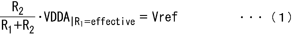
- the operational amplifier 187 receives the signal (Vin) rectified by the rectifier circuit 183 and divided by the resistor 184 and the resistor 185 at one input terminal (+ terminal).
- a constant reference voltage (Vref) from the reference voltage circuit is input to the other input terminal ( ⁇ terminal).
- the modulation signal is used as a control signal for controlling on / off of the switch 186.
- the resistor 184 becomes an effective state or a shorted state in accordance with the switching operation of the switch 186.
- the amplitude difference of R 1 / R 2 * Vref can be obtained on the VDDA signal by turning on / off the switch 186 by the modulation signal. Then, this amplitude difference appears as an impedance fluctuation at the antenna coil terminal via the rectifier circuit 183.
- FIG. 7 shows a feedback system on the VDDA signal, the same applies to the case where a configuration in which the voltage control MOS transistor 188 is arranged between both ends of the antenna coil terminal is employed. The effect of can be obtained.
- the resistor 184 is short-circuited is shown for the sake of simplification.
- the resistance value R 1 of the resistor 184 is divided into several parts, and some of the resistors are effective.
- the impedance can be changed by switching between the state and the shorted state.
- the rectifier circuit 183 may be shared with the rectifier circuit 157 of FIG.
- circuit configurations in FIGS. 3 to 7 are merely examples, and other circuit configurations capable of applying load modulation may be employed.
- the transmission circuit 155 is configured as described above.
- the communication device 101-1 and the communication device 101-2 are arranged at a position where close communication is possible, the communication device 101-1 operates in the reader / writer mode, and the communication device 101-2 is in the tag mode. It shall work.
- the detailed internal configurations of the integrated circuit 112-1 and the external circuit 115-1, and the integrated circuit 112-2 and the external circuit 115-2 are omitted, the configuration shown in FIG. In the following description, “ ⁇ 1” is added to the code of the internal circuit, and “ ⁇ 2” is added to the code of the latter internal circuit.
- a control signal (MODE) is supplied from the host controller 113-1 to the mode control unit 171-1 of the integrated circuit 112-1.
- the mode control unit 171-1 causes each unit of the integrated circuit 112-1 such as the transmission circuit 155-1 and the reception circuit 158-1 to operate in the reader / writer mode according to the control signal (MODE) from the host controller 113-1.
- the host controller 113-1 checks whether another reader / writer is generating a magnetic field around the communication device 101-1, and if the other reader / writer is not generating a magnetic field, the reader / writer mode A control signal (MODE) indicating a transition to is supplied to the mode control unit 171-1.
- a control signal (EN) is supplied from the host controller 113-1 to the external circuit 115-1.
- the switch 193-1 is turned on in accordance with a control signal (EN) from the host controller 113-1.
- power from the power supply 114-1 is supplied to the oscillation circuit 191-1, and the oscillation circuit 191-1 starts generating an oscillation signal.
- the tri-state inverter circuit 194-1 and the tri-state buffer circuit 197-1 transition the output state from the high impedance output state to the normal output state in accordance with the control signal (EN) from the host controller 113-1.
- the tristate inverter circuit 194-1 inverts the oscillation signal from the oscillation circuit 191-1 and supplies it to the filter circuit 195-1.
- the filter circuit 195-1 generates a 13.56 MHz carrier based on the oscillation signal from the tristate inverter circuit 194-1.
- the tristate buffer circuit 197-1 supplies the oscillation signal from the oscillation circuit 191-1 to the filter circuit 198-1.
- the filter circuit 198-1 generates a 13.56 MHz carrier based on the oscillation signal from the tristate buffer circuit 197-1.
- the impedance circuit 196-1 and the impedance circuit 199-1 allow the impedance of the parallel resonant circuit of the antenna circuit 111 to have a predetermined value.
- the external circuit 115-1 when the communication device 101-1 operates in the reader / writer mode, the external circuit 115-1 generates a carrier of 13.56 MHz in the antenna circuit 111-1.
- the host controller 113-1 supplies the data input circuit 153-1 with transmission data to be sent to the communication device 101-2 as the communication destination.
- the communication control unit 172-1 encodes transmission data input from the host controller 113-1 by the Manchester method.
- the transmission circuit 155-1 changes the impedance of the parallel resonance circuit of the antenna circuit 111-1 in accordance with the Manchester encoded transmission data from the communication control unit 172-1, so that the external circuit 115-1 can change the antenna.
- the carrier generated in the circuit 111-1 is load-modulated.
- the modulated signal from the communication device 101-1 is transmitted to the communication device 101-2 of the communication destination by the carrier.
- Communication apparatus 101-2 starts operation by converting an AC voltage obtained from the carrier generated in antenna circuit 111-1 of communication apparatus 101-1 into a DC voltage, and receives a modulated signal from communication apparatus 101-1.
- the response data is transmitted by performing load modulation while receiving.
- a modulation signal generated by load modulation by the communication apparatus 101-2 as the communication destination is induced in the antenna circuit 111-1 of the communication apparatus 101-1.
- the reception circuit 158-1 demodulates the modulation signal based on the output from the rectification circuit 157-1.
- the communication control unit 172-1 decodes the Manchester encoded reception data from the reception circuit 158-1, and supplies it to the host controller 113-1 via the data output circuit 154-1.
- the communication device 101-1 operating in the reader / writer mode has been described above.
- the antenna circuit 111-2 receives the carrier radiated from the antenna circuit 111-1 of the communication device 101-1.
- the power source power may be supplied from the power source 114-2, and the selection of the power source power is performed by the power selection circuit 159-2.
- a control signal (MODE) is supplied from the host controller 113-2 to the mode control unit 171-2.
- the mode control unit 171-2 causes each unit of the integrated circuit 112-2 such as the transmission circuit 155-2 and the reception circuit 158-2 to operate in the tag mode according to the control signal (MODE) from the host controller 113-2. Control.
- the external circuit 115-2 is supplied with a control signal (EN) from the host controller 113-2.
- the switch 193-2 is turned off in accordance with the control signal (EN) from the host controller 113-2. As a result, power from the power supply 114-2 is not supplied to the oscillation circuit 191-2, and generation of the oscillation signal is stopped.
- the tri-state inverter circuit 194-2 and the tri-state buffer circuit 197-2 set the output state to the high impedance output state in accordance with the control signal (EN) from the host controller 113-2. As a result, the outputs of the tristate inverter circuit 194-2 and the tristate buffer circuit 197-2 are in a high impedance state.
- the carrier generated by the communication device 101-1 that is the communication destination is used, and thus the external circuit 115-2 does not generate a carrier.
- the reception circuit 158-2 demodulates the modulation signal based on the output from the rectifier circuit 157-2. .
- the communication control unit 172-2 decodes the Manchester encoded reception data from the reception circuit 158-2 and supplies it to the host controller 113-2 via the data output circuit 154-2.
- the host controller 113-2 supplies the data input circuit 153-2 with transmission data to be returned to the communication apparatus 101-1, which is the communication destination, in accordance with the received data from the data output circuit 154-2.
- the communication control unit 172-2 encodes transmission data input from the host controller 113-2 by the Manchester method.
- the transmission circuit 155-2 performs load modulation on the Manchester-encoded transmission data from the communication control unit 172-2 by changing the impedance of the parallel resonance circuit of the antenna circuit 111-2, and performs communication on the communication device of the communication destination Send to 101-1.
- the modulation signal from the communication device 101-2 is transmitted to the communication device 101-1 of the communication destination by load modulation.
- the communication device 101-2 operating in the tag mode has been described above.
- the integrated circuit 112 when the integrated circuit 112 operates in the reader / writer mode, the carrier generated in the antenna circuit 111 by the external circuit 115 is used, and the parallel resonance circuit of the antenna circuit 111 is determined according to transmission data. By performing load modulation that changes impedance, transmission data is transmitted to a communication destination. Further, when the integrated circuit 112 operates in the tag mode, the integrated circuit 112 receives data transmitted from the communication destination, and transmits transmission data for reply to the received data to the communication destination using load modulation.
- the transmission data is modulated using the same load modulation method as in the tag mode transmission without using the ASK modulation method in the reader / writer mode transmission. It is not necessary to provide a plurality of transmitters, and the transmission circuit can be shared.
- a transmission circuit 155 is provided as a dedicated transmission circuit for the load modulation method. This can be realized by utilizing the fact that a predetermined standard (for example, FeliCa (registered trademark)) uses the same encoding method (for example, Manchester method) when transmitting and receiving data.
- a predetermined standard for example, FeliCa (registered trademark)
- the same encoding method for example, Manchester method
- the same encoding method for example, Manchester method
- the same encoding method is used at the time of data transmission / reception according to a predetermined standard, so that the encoding circuit (not shown) of the communication control unit 172 is also shared. Has been.
- the transmission circuit 155 is shared between the reader / writer mode and the tag mode, and the manufacturing cost is reduced. As a result, the communication apparatus 101 can be provided at low cost.
- the transmission circuit 155 is shared, and the external circuit 115 can be mounted as a separate circuit to generate carriers, so that the integrated circuit 112 is provided at low cost. Also, it is possible to reduce the size of the circuit.
- the communication device 101-1 operates in the reader / writer mode and the communication device 101-2 operates in the tag mode. Conversely, the communication device 101-1 operates in the tag mode. It is also possible for the communication device 101-2 to operate in the reader / writer mode.
- the communication destination is the communication device 101.
- an external device having only one function of the RF tag or the reader / writer may be the communication destination.
- the RF tag and the non-contact IC card may be configured such that the voltage does not rise above a predetermined set voltage due to the relationship with the withstand voltage of the integrated circuit (chip), communication performance, and the like.
- the carrier waveform may be distorted.
- the harmonic component may become a problem due to distortion of the carrier waveform (for example, a sine wave becomes close to a rectangular wave). is there.
- the carrier since the carrier is transmitted in the reader / writer mode, it is necessary to maintain the waveform of the sine wave.
- the tag mode there is no need for the carrier distortion.
- a voltage setting circuit 160 is newly provided in the integrated circuit 112 so that a voltage value corresponding to the operation mode can be set.
- the voltage setting circuit 160 includes, for example, a step-down element (for example, a resistance element or a diode element), a switch for turning on / off these elements depending on an operation state, and a shunt regulator circuit, and a rectifier circuit. 157 is provided in the subsequent stage.
- the voltage setting circuit 160 controls the voltage value of the DC voltage converted by the rectifier circuit 157 so as not to exceed the set voltage in accordance with the control from the mode control unit 171.
- the voltage setting circuit 160 enables the step-down element by the control signal (MODE), and further increases the setting voltage of the shunt regulator circuit, thereby setting the voltage between the antenna coil terminals to 8V. Set to the set voltage.
- the voltage setting circuit 160 disables the step-down element by the control signal (MODE), and further lowers the setting voltage of the shunt regulator circuit so that the voltage between the antenna coil terminals is 4V. Set to a certain set voltage.
- the integrated circuit 112 when operating in the reader / writer mode, the carrier sine wave waveform is maintained even when the voltage is set to be higher in order to obtain higher output. Further, in the integrated circuit 112, when operating in the tag mode, a lower set voltage is set, so that damage to the integrated circuit (chip) can be reliably prevented.
- the voltage setting circuit 160 can set the voltage as the setting voltage regardless of the operation mode.
- the tag mode setting voltage may be fixedly set.
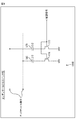
- FIG. 10 is a diagram illustrating a configuration of an embodiment of a communication system to which the present technology is applied.
- the communication system 201 includes a communication device 102, a carrier generation device 211, and an RF tag 212.
- the communication device 102 operates in the reader / writer mode, and performs near field communication with the communication destination RF tag 212.
- the communication device 102 includes an antenna circuit 111, an integrated circuit 112, a host controller 113, and a power source 114.
- the antenna circuit 111 to the power source 114 are configured similarly to the antenna circuit 111 to the power source 114 in FIG.
- the communication device 102 has a configuration in which the external circuit 115 for generating a carrier is removed as compared with the communication device 101 of FIG. Therefore, in the communication system 201, a carrier generating device 211 for generating a carrier is provided instead of the external circuit 115.
- the carrier generating device 211 includes an oscillation circuit 251, a crystal oscillator 252, a power supply 253, a switch 254, a coil 255, and a capacitor 256.
- the oscillation circuit 251 generates an oscillation signal corresponding to the vibration frequency of the crystal oscillator 252.
- the power source 253 supplies power to the oscillation circuit 251 when the switch 254 is turned on. However, the switch 254 performs an on / off switching operation in accordance with control from a host controller (not shown).
- the coil 255 and the capacitor 256 form a parallel resonance circuit.
- L12 represents the inductance of the coil 255
- C14 represents the capacitance of the capacitor.
- the operation of the carrier generating device 211 will be described.
- the switch 254 when the switch 254 is turned on from the off state, the power source power from the power source 253 is supplied to the oscillation circuit 251.
- the oscillation circuit 251 starts operation with power supply power from the power supply 253 and generates an oscillation signal corresponding to the vibration frequency of the crystal oscillator 252.
- This oscillation signal is applied to a parallel resonance circuit composed of a coil 255 and a capacitor 256, and a magnetic field is generated. As a result, a carrier having a predetermined frequency (13.56 MHz) is generated in the antenna circuit 111 of the communication apparatus 102.
- the antenna circuit 111 is connected in parallel according to the transmission data from the communication control unit 172.
- the carrier generated in the antenna circuit 111 by the carrier generating device 211 is load-modulated.
- the modulated signal from the communication apparatus 102 is transmitted to the RF tag 212 of the communication destination.
- a modulation signal generated by load modulation by the communication target RF tag 212 is induced.
- the receiving circuit 158 demodulates the modulation signal generated in the antenna circuit 111 based on the output from the rectifier circuit 157 and supplies the received data obtained thereby to the communication control unit 172.
- the communication apparatus 102 does not have the external circuit 115, and load modulation is performed on the carrier generated in the antenna circuit 111 by the carrier generation device 211, so that the transmission data is communicated. It is transmitted to the previous RF tag 212.
- the communication device 102 since the communication device 102 modulates transmission data using the same load modulation method when transmitting in the reader / writer mode and the tag mode, data transmission / reception is performed using the carrier generated by the carrier generation device 211. Can be done.
- This configuration eliminates the need for mounting the external circuit 115 in the communication device 102, thereby enabling the communication device 102 to be downsized and provided at a low cost.
- the communication system 201 is configured as described above.
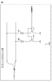
- FIG. 11 is a diagram illustrating a configuration of an embodiment of an electronic device to which the present technology is applied.
- the electronic device 301 is, for example, a portable information device such as a mobile phone, a smartphone, or a tablet PC, or a mobile communication terminal. As illustrated in FIG. 11, the electronic device 301 includes a communication device 101, a control unit 311, a memory unit 312, an operation unit 313, a display unit 314, a wireless communication unit 315, and an audio processing unit 316.
- the control unit 311 controls the operation of each unit of the electronic device 301.
- the memory unit 312 holds various data according to control from the control unit 311.
- control unit 311 has a function as the above-described host controller 113 (FIG. 2 and the like), and controls the operation mode of the communication apparatus 101.
- the communication device 101 operates in a reader / writer mode or a tag mode in accordance with control from the control unit 311.
- the communication device 101 When operating in the reader / writer mode, the communication device 101 transmits transmission data to a communication destination RF tag (not shown) using a load modulation method in accordance with control from the control unit 311. In addition, the communication apparatus 101 receives return data sent from the communication destination RF tag in accordance with control from the control unit 311.
- the communication apparatus 101 when the communication apparatus 101 operates in the tag mode, the communication apparatus 101 receives data transmitted from a reader / writer (not shown) as a communication destination in accordance with control from the control unit 311. In addition, the communication apparatus 101 transmits the return transmission data to the communication destination reader / writer using the load modulation method in accordance with the control from the control unit 311.
- the operation unit 313 supplies an operation signal corresponding to a user operation to the control unit 311.
- the control unit 311 controls the operation of each unit of the electronic device 301 in accordance with an operation signal from the operation unit 313.
- the operation unit 313 may be a GUI (Graphical User Interface) image displayed on the screen of the display unit 314 having a touch panel, for example, in addition to a physical button.
- GUI Graphic User Interface
- the display unit 314 includes a display device such as a liquid crystal display (LCD).
- the display unit 314 displays various types of information such as text and images according to control from the control unit 311.
- the wireless communication unit 315 performs wireless communication with a predetermined server via a network such as the Internet in accordance with control from the control unit 311.
- the voice processing unit 316 includes a device for performing a voice call such as a microphone or a speaker.
- the voice processing unit 316 performs voice input processing or voice output processing in accordance with control from the control unit 311.
- the electronic device 301 is configured as described above.
- the communication device 101 since the communication device 101 is mounted on the electronic device 301, for example, when another electronic device having an RF tag function is held over the electronic device 301, the communication device 101 operates in the reader / writer mode. Thus, data transmission / reception is performed with other electronic devices. Further, for example, when the electronic device 301 is placed over a reader / writer provided in a ticket gate of a station or a cash register of a store, the communication device 101 operates in a tag mode and transmits data to and from the reader / writer. Send and receive.
- the transmission circuit 155 is shared by the reader / writer mode and the tag mode, and the manufacturing cost is reduced.
- the communication device 101 FIG. 2
- the communication device 102 FIG. 10
- the electronic device 301 FIG. 11
- the present technology can meet the demand.
- the integrated circuit 112 (FIG. 2 and the like), there has conventionally been a need for a circuit for generating carriers such as the oscillation circuit 15 and the crystal oscillator 16 as shown in FIG.
- the external circuit 115 can be mounted as a separate circuit, the integrated circuit 112 can be provided at a low cost and the circuit can be downsized.
- the communication device 102 does not include the external circuit 115 that is a separate circuit from the integrated circuit 112, and instead of using the external circuit 115, a carrier generated by the carrier generating device 211 is used to transmit data. Can be sent and received. As a result, the proximity communication via the carrier generating device 211 is possible, so that the communication device 102 can be reduced in size and cost. Furthermore, since the external circuit 115 is not mounted on the communication device 102, power consumption can be reduced accordingly.
- the integrated circuit 112 and the external circuit 115 are mounted on the same substrate, it is possible to construct a communication system without using the carrier generating device 211, and the integrated circuit 112 and the external circuit 115 are mounted. Proximity communication between all electronic devices equipped with modules can be performed.
- the ASK modulation method when operating in the reader / writer mode, the ASK modulation method is used in which the carrier is driven with a low impedance and the amplitude is forcibly modulated. It is necessary to change the level forcibly while driving. For this reason, transmission buffer circuits 58 and 59 are provided after the transmission circuit 57.
- the load modulation method is also used when operating in the reader / writer mode. In the load modulation method, an impedance of a certain level (for example, about several hundred to 1 K ⁇ ) Since modulation is applied according to the amount of change, the transmission buffer circuits 58 and 59 are not required in the integrated circuit 112 (FIG. 2 and the like). For this reason, the transmission buffer circuits 58 and 59 need not be provided, so that the size and cost can be reduced.
- the RF tag has been described as the communication target when the communication device 101, the communication device 102, or the electronic device 301 operates in the reader / writer mode.
- the present technology is not limited to this, for example, Communication devices in general that perform proximity communication with an RFID reader / writer using an electromagnetic coupling method such as a non-contact type IC card can be targeted for communication.
- the present technology can take the following configurations.
- An antenna section A transmission unit that modulates transmission data and transmits the data to a communication destination via the antenna unit; A receiving unit for receiving and demodulating modulated reception data from the communication destination via the antenna unit;
- the transmission unit and the reception unit are in either one of a first operation mode that operates as an RFID (Radio Frequency IDentification) reader / writer and a second operation mode that operates as a communication target of the RFID reader / writer.
- RFID Radio Frequency IDentification
- the transmitter is When operating in the first operation mode, using the first carrier generated in the antenna unit and performing load modulation that changes the impedance of the antenna unit according to the transmission data, the transmission data To the communication target, When operating in the second operation mode, using the second carrier received by the antenna unit, and performing load modulation that changes the impedance of the antenna unit according to the transmission data, the transmission data A communication device that transmits to the RFID reader / writer.
- the communication device according to (1) further including a carrier generation unit that generates the first carrier.
- the carrier generation unit causes the impedance of the antenna unit to have a predetermined value.
- the first carrier is generated by an external carrier generation device.
- the communication apparatus according to any one of (1) to (4), wherein the transmission data and the reception data are encoded by the same encoding method.
- An antenna section A transmission unit that modulates transmission data and transmits the data to a communication destination via the antenna unit;
- a communication method of a communication device comprising: a receiving unit that receives and demodulates modulated reception data from the communication destination via the antenna unit;
- the transmission unit and the reception unit operate in one of the first operation mode that operates as an RFID reader / writer and the second operation mode that operates as a communication target of the RFID reader / writer,
- the transmitter is When operating in the first operation mode, using the first carrier generated in the antenna unit and performing load modulation that changes the impedance of the antenna unit according to the transmission data, the transmission data To the communication target, When operating in the second operation mode, using the second carrier received by the antenna unit, and performing load modulation that changes the impedance of the antenna unit according to the transmission data, the transmission data
- a communication method including a step of transmitting a message to an RFID reader / writer.
- a transmission circuit that modulates transmission data and transmits it to a communication destination via an external antenna circuit; A receiving circuit for receiving and demodulating the modulated received data from the communication destination via the antenna circuit;
- the transmission circuit and the reception circuit operate in one of the first operation mode that operates as an RFID reader / writer and the second operation mode that operates as a communication target of the RFID reader / writer,
- the transmission circuit includes: When operating in the first operation mode, using the first carrier generated in the antenna circuit, and performing load modulation that changes the impedance of the antenna circuit according to the transmission data, the transmission data To the communication target, When operating in the second operation mode, using the second carrier received by the antenna circuit, and performing load modulation that changes the impedance of the antenna circuit according to the transmission data, the transmission data An integrated circuit that transmits to the RFID reader / writer.
- a transmission circuit that modulates transmission data and transmits it to a communication destination via an external antenna circuit In a communication method of an integrated circuit comprising: a reception circuit that receives and demodulates received data modulated from the communication destination via the antenna circuit; The transmission circuit and the reception circuit operate in one of the first operation mode in which the RFID reader / writer operates and the second operation mode in which the RFID reader / writer operates as a communication target; The transmission circuit is When operating in the first operation mode, using the first carrier generated in the antenna circuit, and performing load modulation that changes the impedance of the antenna circuit according to the transmission data, the transmission data To the communication target, When operating in the second operation mode, using the second carrier received by the antenna circuit, and performing load modulation that changes the impedance of the antenna circuit according to the transmission data, the transmission data A communication method including a step of transmitting a message to an RFID reader / writer.
- An antenna section A transmission unit that modulates transmission data and transmits the data to a communication destination via the antenna unit; A receiving unit for receiving and demodulating modulated reception data from the communication destination via the antenna unit;
- the transmission unit and the reception unit operate in one operation mode of a first operation mode that operates as an RFID reader / writer and a second operation mode that operates as a communication target of the RFID reader / writer,
- the transmitter is When operating in the first operation mode, using the first carrier generated in the antenna unit and performing load modulation that changes the impedance of the antenna unit according to the transmission data, the transmission data To the communication target, When operating in the second operation mode, using the second carrier received by the antenna unit, and performing load modulation that changes the impedance of the antenna unit according to the transmission data, the transmission data
- 101, 102 communication device 111 antenna circuit, 112 integrated circuit, 113 host controller, 114 power supply, 115 external circuit, 131 coil, 132 capacitor, 151 control unit, 152 nonvolatile memory, 153 data input circuit, 154 data output circuit, 155, 155A, 155B, 155C, 155D, 155E transmission circuit, 156 clock extraction circuit, 157 rectification circuit, 158 reception circuit, 159 power selection circuit, 160 voltage setting circuit, 171 mode control unit, 172 communication control unit, 191 oscillation circuit , 192 crystal oscillator, 193 switch, 194 tri-state inverter circuit, 195, 198 filter circuit, 196, 199 Imp Nsu circuit, 197 tri-state buffer circuit, 201 communication system, 211 carrier generation equipment, 212 RF tag, 251 oscillator, 252 a crystal oscillator, 253 a power supply, 254 switch, 255 a coil, 256 a capacitor, 301 the electronic device, 311 control unit
Abstract
Description
<通信装置の構成>
図3は、抵抗とMOSスイッチから構成される送信回路155Aの構成を示す図である。図3に示すように、送信回路155Aは、抵抗175とMOSトランジスタ177とが直列に接続され、抵抗176とMOSトランジスタ178とが直列に接続されて構成される。ただし、図3において、R11は抵抗175の抵抗値を、R12は抵抗176の抵抗値をそれぞれ示している。
図4は、コンデンサとMOSスイッチから構成される送信回路155Bの構成を示す図である。図4に示すように、送信回路155Bは、コンデンサ179とMOSトランジスタ177とが直列に接続され、コンデンサ180とMOSトランジスタ178とが直列に接続されて構成される。ただし、図4において、C12はコンデンサ179の容量、C13はコンデンサ180の容量をそれぞれ示している。
図5は、ダイオードとMOSスイッチから構成される送信回路155Cの構成を示す図である。図5に示すように、送信回路155Cは、ダイオード181とMOSトランジスタ177とが直列に接続され、ダイオード182とMOSトランジスタ178とが直列に接続されて構成される。
図6は、ダイオードと抵抗の組み合わせとMOSスイッチから構成される送信回路155Dの構成を示す図である。図6に示すように、送信回路155Dは、ダイオード181と、抵抗175と、MOSトランジスタ177とが直列に接続され、ダイオード182と、抵抗176と、MOSトランジスタ178とが直列に接続されて構成される。
図7は、フィードバック制御を用いて負荷変調を制御する送信回路155Eの構成を示す図である。図7に示すように、送信回路155Eは、整流回路183、抵抗184、抵抗185、スイッチ186、オペアンプ187、及び、MOSトランジスタ188から構成される。ただし、図7において、R1は抵抗184の抵抗値を、R2は抵抗185の抵抗値をそれぞれ示している。

まず、リーダライタモードで動作する通信装置101-1について説明する。
次に、タグモードで動作する通信装置101-2の動作について説明する。
<通信システムの構成>
<電子機器の構成>
アンテナ部と、
送信データを変調して、前記アンテナ部を介して通信先に送信する送信部と、
前記通信先からの変調された受信データを、前記アンテナ部を介して受信して復調する受信部と
を備え、
前記送信部及び前記受信部は、RFID(Radio Frequency IDentification)リーダライタとして動作する第1の動作モードと、RFIDリーダライタの通信対象として動作する第2の動作モードのうちいずれか一方の動作モードで動作し、
前記送信部は、
前記第1の動作モードで動作する場合、前記アンテナ部にて発生した第1のキャリアを用い、前記送信データに応じて、前記アンテナ部のインピーダンスを変化させる負荷変調を行うことで、前記送信データを通信対象に送信し、
前記第2の動作モードで動作する場合、前記アンテナ部にて受信した第2のキャリアを用い、前記送信データに応じて、前記アンテナ部のインピーダンスを変化させる負荷変調を行うことで、前記送信データをRFIDリーダライタに送信する
通信装置。
(2)
前記第1のキャリアを生成するキャリア生成部をさらに備える
(1)に記載の通信装置。
(3)
前記キャリア生成部は、前記アンテナ部のインピーダンスが所定の大きさの値を持つようにする
(2)に記載の通信装置。
(4)
前記第1のキャリアは、外部のキャリア発生装置により発生される
(1)に記載の通信装置。
(5)
前記送信データと前記受信データとは、同一の符号化方式により符号化される
(1)乃至(4)のいずれか一項に記載の通信装置。
(6)
前記アンテナ部の電磁誘導により発生する電源電圧を、前記動作モードに応じて制限する電圧設定部をさらに備える
(1)乃至(5)のいずれか一項に記載の通信装置。
(7)
アンテナ部と、
送信データを変調して、前記アンテナ部を介して通信先に送信する送信部と、
前記通信先からの変調された受信データを、前記アンテナ部を介して受信して復調する受信部と
を備える通信装置の通信方法において、
前記送信部及び前記受信部が、RFIDリーダライタとして動作する第1の動作モードと、RFIDリーダライタの通信対象として動作する第2の動作モードのうちいずれか一方の動作モードで動作し、
前記送信部が、
前記第1の動作モードで動作する場合、前記アンテナ部にて発生した第1のキャリアを用い、前記送信データに応じて、前記アンテナ部のインピーダンスを変化させる負荷変調を行うことで、前記送信データを通信対象に送信し、
前記第2の動作モードで動作する場合、前記アンテナ部にて受信した第2のキャリアを用い、前記送信データに応じて、前記アンテナ部のインピーダンスを変化させる負荷変調を行うことで、前記送信データをRFIDリーダライタに送信する
ステップを含む通信方法。
(8)
送信データを変調して、外部のアンテナ回路を介して通信先に送信する送信回路と、
前記通信先からの変調された受信データを、前記アンテナ回路を介して受信して復調する受信回路と
を備え、
前記送信回路及び前記受信回路は、RFIDリーダライタとして動作する第1の動作モードと、RFIDリーダライタの通信対象として動作する第2の動作モードのうちいずれか一方の動作モードで動作し、
前記送信回路は、
前記第1の動作モードで動作する場合、前記アンテナ回路にて発生した第1のキャリアを用い、前記送信データに応じて、前記アンテナ回路のインピーダンスを変化させる負荷変調を行うことで、前記送信データを通信対象に送信し、
前記第2の動作モードで動作する場合、前記アンテナ回路にて受信した第2のキャリアを用い、前記送信データに応じて、前記アンテナ回路のインピーダンスを変化させる負荷変調を行うことで、前記送信データをRFIDリーダライタに送信する
集積回路。
(9)
前記第1のキャリアは、外部のキャリア生成回路により発生される
(8)に記載の集積回路。
(10)
前記キャリア生成回路は、前記アンテナ回路のインピーダンスが所定の大きさの値を持つようにする
(9)に記載の集積回路。
(11)
前記送信データと前記受信データとは、同一の符号化方式により符号化される
(8)乃至(10)のいずれか一項に記載の集積回路。
(12)
前記アンテナ回路の電磁誘導により発生する電源電圧を、前記動作モードに応じて制限する電圧設定回路をさらに備える
(8)乃至(11)のいずれか一項に記載の集積回路。
(13)
送信データを変調して、外部のアンテナ回路を介して通信先に送信する送信回路と、
前記通信先からの変調された受信データを、前記アンテナ回路を介して受信して復調する受信回路と
を備える集積回路の通信方法において、
前記送信回路及び前記受信回路が、RFIDリーダライタとして動作する第1の動作モードと、RFIDリーダライタの通信対象として動作する第2の動作モードのうちいずれか一方の動作モードで動作し、
前記送信回路が、
前記第1の動作モードで動作する場合、前記アンテナ回路にて発生した第1のキャリアを用い、前記送信データに応じて、前記アンテナ回路のインピーダンスを変化させる負荷変調を行うことで、前記送信データを通信対象に送信し、
前記第2の動作モードで動作する場合、前記アンテナ回路にて受信した第2のキャリアを用い、前記送信データに応じて、前記アンテナ回路のインピーダンスを変化させる負荷変調を行うことで、前記送信データをRFIDリーダライタに送信する
ステップを含む通信方法。
(14)
アンテナ部と、
送信データを変調して、前記アンテナ部を介して通信先に送信する送信部と、
前記通信先からの変調された受信データを、前記アンテナ部を介して受信して復調する受信部と
を有し、
前記送信部及び前記受信部は、RFIDリーダライタとして動作する第1の動作モードと、RFIDリーダライタの通信対象として動作する第2の動作モードのうちいずれか一方の動作モードで動作し、
前記送信部は、
前記第1の動作モードで動作する場合、前記アンテナ部にて発生した第1のキャリアを用い、前記送信データに応じて、前記アンテナ部のインピーダンスを変化させる負荷変調を行うことで、前記送信データを通信対象に送信し、
前記第2の動作モードで動作する場合、前記アンテナ部にて受信した第2のキャリアを用い、前記送信データに応じて、前記アンテナ部のインピーダンスを変化させる負荷変調を行うことで、前記送信データをRFIDリーダライタに送信する
通信装置を搭載した電子機器。
Claims (14)
- アンテナ部と、
送信データを変調して、前記アンテナ部を介して通信先に送信する送信部と、
前記通信先からの変調された受信データを、前記アンテナ部を介して受信して復調する受信部と
を備え、
前記送信部及び前記受信部は、RFID(Radio Frequency IDentification)リーダライタとして動作する第1の動作モードと、RFIDリーダライタの通信対象として動作する第2の動作モードのうちいずれか一方の動作モードで動作し、
前記送信部は、
前記第1の動作モードで動作する場合、前記アンテナ部にて発生した第1のキャリアを用い、前記送信データに応じて、前記アンテナ部のインピーダンスを変化させる負荷変調を行うことで、前記送信データを通信対象に送信し、
前記第2の動作モードで動作する場合、前記アンテナ部にて受信した第2のキャリアを用い、前記送信データに応じて、前記アンテナ部のインピーダンスを変化させる負荷変調を行うことで、前記送信データをRFIDリーダライタに送信する
通信装置。 - 前記第1のキャリアを生成するキャリア生成部をさらに備える
請求項1に記載の通信装置。 - 前記キャリア生成部は、前記アンテナ部のインピーダンスが所定の大きさの値を持つようにする
請求項2に記載の通信装置。 - 前記第1のキャリアは、外部のキャリア発生装置により発生される
請求項1に記載の通信装置。 - 前記送信データと前記受信データとは、同一の符号化方式により符号化される
請求項1に記載の通信装置。 - 前記アンテナ部の電磁誘導により発生する電源電圧を、前記動作モードに応じて制限する電圧設定部をさらに備える
請求項1に記載の通信装置。 - アンテナ部と、
送信データを変調して、前記アンテナ部を介して通信先に送信する送信部と、
前記通信先からの変調された受信データを、前記アンテナ部を介して受信して復調する受信部と
を備える通信装置の通信方法において、
前記送信部及び前記受信部が、RFIDリーダライタとして動作する第1の動作モードと、RFIDリーダライタの通信対象として動作する第2の動作モードのうちいずれか一方の動作モードで動作し、
前記送信部が、
前記第1の動作モードで動作する場合、前記アンテナ部にて発生した第1のキャリアを用い、前記送信データに応じて、前記アンテナ部のインピーダンスを変化させる負荷変調を行うことで、前記送信データを通信対象に送信し、
前記第2の動作モードで動作する場合、前記アンテナ部にて受信した第2のキャリアを用い、前記送信データに応じて、前記アンテナ部のインピーダンスを変化させる負荷変調を行うことで、前記送信データをRFIDリーダライタに送信する
ステップを含む通信方法。 - 送信データを変調して、外部のアンテナ回路を介して通信先に送信する送信回路と、
前記通信先からの変調された受信データを、前記アンテナ回路を介して受信して復調する受信回路と
を備え、
前記送信回路及び前記受信回路は、RFIDリーダライタとして動作する第1の動作モードと、RFIDリーダライタの通信対象として動作する第2の動作モードのうちいずれか一方の動作モードで動作し、
前記送信回路は、
前記第1の動作モードで動作する場合、前記アンテナ回路にて発生した第1のキャリアを用い、前記送信データに応じて、前記アンテナ回路のインピーダンスを変化させる負荷変調を行うことで、前記送信データを通信対象に送信し、
前記第2の動作モードで動作する場合、前記アンテナ回路にて受信した第2のキャリアを用い、前記送信データに応じて、前記アンテナ回路のインピーダンスを変化させる負荷変調を行うことで、前記送信データをRFIDリーダライタに送信する
集積回路。 - 前記第1のキャリアは、外部のキャリア生成回路により発生される
請求項8に記載の集積回路。 - 前記キャリア生成回路は、前記アンテナ回路のインピーダンスが所定の大きさの値を持つようにする
請求項9に記載の集積回路。 - 前記送信データと前記受信データとは、同一の符号化方式により符号化される
請求項8に記載の集積回路。 - 前記アンテナ回路の電磁誘導により発生する電源電圧を、前記動作モードに応じて制限する電圧設定回路をさらに備える
請求項8に記載の集積回路。 - 送信データを変調して、外部のアンテナ回路を介して通信先に送信する送信回路と、
前記通信先からの変調された受信データを、前記アンテナ回路を介して受信して復調する受信回路と
を備える集積回路の通信方法において、
前記送信回路及び前記受信回路が、RFIDリーダライタとして動作する第1の動作モードと、RFIDリーダライタの通信対象として動作する第2の動作モードのうちいずれか一方の動作モードで動作し、
前記送信回路が、
前記第1の動作モードで動作する場合、前記アンテナ回路にて発生した第1のキャリアを用い、前記送信データに応じて、前記アンテナ回路のインピーダンスを変化させる負荷変調を行うことで、前記送信データを通信対象に送信し、
前記第2の動作モードで動作する場合、前記アンテナ回路にて受信した第2のキャリアを用い、前記送信データに応じて、前記アンテナ回路のインピーダンスを変化させる負荷変調を行うことで、前記送信データをRFIDリーダライタに送信する
ステップを含む通信方法。 - アンテナ部と、
送信データを変調して、前記アンテナ部を介して通信先に送信する送信部と、
前記通信先からの変調された受信データを、前記アンテナ部を介して受信して復調する受信部と
を有し、
前記送信部及び前記受信部は、RFIDリーダライタとして動作する第1の動作モードと、RFIDリーダライタの通信対象として動作する第2の動作モードのうちいずれか一方の動作モードで動作し、
前記送信部は、
前記第1の動作モードで動作する場合、前記アンテナ部にて発生した第1のキャリアを用い、前記送信データに応じて、前記アンテナ部のインピーダンスを変化させる負荷変調を行うことで、前記送信データを通信対象に送信し、
前記第2の動作モードで動作する場合、前記アンテナ部にて受信した第2のキャリアを用い、前記送信データに応じて、前記アンテナ部のインピーダンスを変化させる負荷変調を行うことで、前記送信データをRFIDリーダライタに送信する
通信装置を搭載した電子機器。
Priority Applications (6)
| Application Number | Priority Date | Filing Date | Title |
|---|---|---|---|
| EP13863384.7A EP2933757B1 (en) | 2012-12-12 | 2013-11-28 | Communication device, communication method, integrated circuit, and electronic instrument |
| KR1020157014538A KR102096681B1 (ko) | 2012-12-12 | 2013-11-28 | 통신 장치, 통신 방법, 집적 회로, 및 전자 기기 |
| CN201380063335.1A CN104823204B (zh) | 2012-12-12 | 2013-11-28 | 通信设备,通信方法,集成电路和电子仪器 |
| US14/441,321 US9904820B2 (en) | 2012-12-12 | 2013-11-28 | Communication device, communication method, integrated circuit, and electronic instrument |
| JP2014551967A JP6249238B2 (ja) | 2012-12-12 | 2013-11-28 | 通信装置、通信方法、及び、電子機器 |
| HK15111698.5A HK1211118A1 (en) | 2012-12-12 | 2015-11-27 | Communication device, communication method, integrated circuit, and electronic instrument |
Applications Claiming Priority (2)
| Application Number | Priority Date | Filing Date | Title |
|---|---|---|---|
| JP2012271030 | 2012-12-12 | ||
| JP2012-271030 | 2012-12-12 |
Publications (1)
| Publication Number | Publication Date |
|---|---|
| WO2014091934A1 true WO2014091934A1 (ja) | 2014-06-19 |
Family
ID=50934227
Family Applications (1)
| Application Number | Title | Priority Date | Filing Date |
|---|---|---|---|
| PCT/JP2013/082014 WO2014091934A1 (ja) | 2012-12-12 | 2013-11-28 | 通信装置、通信方法、集積回路、及び、電子機器 |
Country Status (7)
| Country | Link |
|---|---|
| US (1) | US9904820B2 (ja) |
| EP (1) | EP2933757B1 (ja) |
| JP (1) | JP6249238B2 (ja) |
| KR (1) | KR102096681B1 (ja) |
| CN (1) | CN104823204B (ja) |
| HK (1) | HK1211118A1 (ja) |
| WO (1) | WO2014091934A1 (ja) |
Cited By (2)
| Publication number | Priority date | Publication date | Assignee | Title |
|---|---|---|---|---|
| JP2019121673A (ja) * | 2018-01-04 | 2019-07-22 | ラピスセミコンダクタ株式会社 | 半導体装置および半導体モジュール |
| WO2020241670A1 (ja) * | 2019-05-28 | 2020-12-03 | ラピスセミコンダクタ株式会社 | 通知応答回路 |
Families Citing this family (10)
| Publication number | Priority date | Publication date | Assignee | Title |
|---|---|---|---|---|
| US20120203620A1 (en) | 2010-11-08 | 2012-08-09 | Douglas Howard Dobyns | Techniques For Wireless Communication Of Proximity Based Marketing |
| US8929809B2 (en) | 2011-03-22 | 2015-01-06 | Radeum, Inc. | Techniques for wireless communication of proximity based content |
| US8880100B2 (en) | 2011-03-23 | 2014-11-04 | Radium, Inc. | Proximity based social networking |
| JP6128986B2 (ja) * | 2013-06-24 | 2017-05-17 | 任天堂株式会社 | 通信システム、通信端末装置、通信プログラム、および通信方法 |
| US9621228B2 (en) | 2014-08-29 | 2017-04-11 | Freelinc Technologies | Spatially aware communications using radio frequency (RF) communications standards |
| US10164685B2 (en) | 2014-12-31 | 2018-12-25 | Freelinc Technologies Inc. | Spatially aware wireless network |
| CN107094037B (zh) * | 2017-03-24 | 2019-10-25 | 深圳市文鼎创数据科技有限公司 | 动态令牌的前端硬件电路及其授种子或生产配置的方法 |
| CN106909865B (zh) * | 2017-03-24 | 2019-10-25 | 深圳市文鼎创数据科技有限公司 | 近场通信前端硬件电路、终端、读写器、系统以及方法 |
| CN109426164B (zh) * | 2017-08-25 | 2021-06-08 | 上海芯龙半导体技术股份有限公司 | 一种用于中央空调系统中信号传输的载波集成电路 |
| US20220092280A1 (en) * | 2019-12-31 | 2022-03-24 | Queclink Wireless Solutions Co., Ltd. | Rfid tag information reading apparatus and method |
Citations (3)
| Publication number | Priority date | Publication date | Assignee | Title |
|---|---|---|---|---|
| JP2008010011A (ja) * | 2007-08-20 | 2008-01-17 | Sony Corp | 通信装置 |
| JP2010050515A (ja) * | 2008-08-19 | 2010-03-04 | Sony Corp | 無線通信装置と受電装置 |
| JP4797991B2 (ja) | 2005-04-15 | 2011-10-19 | ソニー株式会社 | 通信装置、それを搭載した非接触型icカード、および情報機器 |
Family Cites Families (10)
| Publication number | Priority date | Publication date | Assignee | Title |
|---|---|---|---|---|
| JP4501241B2 (ja) * | 2000-07-10 | 2010-07-14 | ソニー株式会社 | Icカード及びicカードのデータ通信方法 |
| EP1644872B1 (en) | 2003-07-22 | 2009-12-09 | Nokia Corporation | Reader device for radio frequency identification transponder with transponder functionality |
| JP2006067448A (ja) * | 2004-08-30 | 2006-03-09 | Ricoh Co Ltd | 通信装置およびこの通信装置を備えた携帯電子機器 |
| US7729660B2 (en) * | 2005-04-15 | 2010-06-01 | Sony Corporation | Communication device, non-contact type IC card mounting same, and information apparatus |
| US8269630B2 (en) * | 2005-12-09 | 2012-09-18 | Tego Inc. | Methods and systems of a multiple radio frequency network node RFID tag |
| JP2007219585A (ja) * | 2006-02-14 | 2007-08-30 | Seiko Epson Corp | 非接触通信方式および非接触通信システム |
| JP4748211B2 (ja) * | 2008-12-02 | 2011-08-17 | ソニー株式会社 | 通信装置、並びに適応等化装置 |
| JP2011060086A (ja) * | 2009-09-11 | 2011-03-24 | Ricoh Co Ltd | Rfidタグ、リーダ・ライタ及びrfidシステム |
| JP2011215865A (ja) * | 2010-03-31 | 2011-10-27 | Sony Corp | 信号処理装置及び信号処理方法 |
| US9397726B2 (en) * | 2010-08-23 | 2016-07-19 | Radeum, Inc. | System and method for communicating between near field communication devices within a target region using near field communication |
-
2013
- 2013-11-28 US US14/441,321 patent/US9904820B2/en active Active
- 2013-11-28 CN CN201380063335.1A patent/CN104823204B/zh not_active Expired - Fee Related
- 2013-11-28 JP JP2014551967A patent/JP6249238B2/ja active Active
- 2013-11-28 KR KR1020157014538A patent/KR102096681B1/ko active IP Right Grant
- 2013-11-28 EP EP13863384.7A patent/EP2933757B1/en active Active
- 2013-11-28 WO PCT/JP2013/082014 patent/WO2014091934A1/ja active Application Filing
-
2015
- 2015-11-27 HK HK15111698.5A patent/HK1211118A1/xx unknown
Patent Citations (3)
| Publication number | Priority date | Publication date | Assignee | Title |
|---|---|---|---|---|
| JP4797991B2 (ja) | 2005-04-15 | 2011-10-19 | ソニー株式会社 | 通信装置、それを搭載した非接触型icカード、および情報機器 |
| JP2008010011A (ja) * | 2007-08-20 | 2008-01-17 | Sony Corp | 通信装置 |
| JP2010050515A (ja) * | 2008-08-19 | 2010-03-04 | Sony Corp | 無線通信装置と受電装置 |
Non-Patent Citations (1)
| Title |
|---|
| See also references of EP2933757A4 |
Cited By (5)
| Publication number | Priority date | Publication date | Assignee | Title |
|---|---|---|---|---|
| JP2019121673A (ja) * | 2018-01-04 | 2019-07-22 | ラピスセミコンダクタ株式会社 | 半導体装置および半導体モジュール |
| US11264838B2 (en) | 2018-01-04 | 2022-03-01 | Lapis Semiconductor Co., Ltd. | Semiconductor device and semiconductor module |
| JP7115723B2 (ja) | 2018-01-04 | 2022-08-09 | ラピスセミコンダクタ株式会社 | 半導体装置および半導体モジュール |
| WO2020241670A1 (ja) * | 2019-05-28 | 2020-12-03 | ラピスセミコンダクタ株式会社 | 通知応答回路 |
| JP7382401B2 (ja) | 2019-05-28 | 2023-11-16 | ラピスセミコンダクタ株式会社 | 通知応答回路 |
Also Published As
| Publication number | Publication date |
|---|---|
| US9904820B2 (en) | 2018-02-27 |
| KR20150094614A (ko) | 2015-08-19 |
| EP2933757A1 (en) | 2015-10-21 |
| EP2933757B1 (en) | 2019-05-01 |
| EP2933757A4 (en) | 2016-07-13 |
| HK1211118A1 (en) | 2016-05-13 |
| US20150254481A1 (en) | 2015-09-10 |
| CN104823204B (zh) | 2018-08-21 |
| JPWO2014091934A1 (ja) | 2017-01-05 |
| KR102096681B1 (ko) | 2020-04-02 |
| CN104823204A (zh) | 2015-08-05 |
| JP6249238B2 (ja) | 2017-12-20 |
Similar Documents
| Publication | Publication Date | Title |
|---|---|---|
| JP6249238B2 (ja) | 通信装置、通信方法、及び、電子機器 | |
| KR101226213B1 (ko) | 전원공급장치의 전압 추출 수단을 포함하는 유도성 결합리더 | |
| US9367713B2 (en) | Contactless communication device | |
| US8897699B2 (en) | Reducing emissions in a near field communications (NFC) capable device | |
| US8099045B2 (en) | Near field communication system and associated apparatus | |
| US10148321B2 (en) | Antenna for near field communication, accessory and electronic device including the same | |
| JP5780894B2 (ja) | 非接触給電システム | |
| JP5177270B2 (ja) | 通信装置、通信システム、および通信方法 | |
| CN108737999B (zh) | 近场通信装置 | |
| JP2007288718A (ja) | 情報処理端末,icカード,携帯型通信装置,無線通信方法,およびプログラム | |
| WO2007003978A1 (en) | Device, module and method for shared antenna operation in a rfid technology based communication environment | |
| JP4618672B2 (ja) | 半導体集積回路および無線通信装置 | |
| US9041515B2 (en) | Apparatus comprising display driving integrated circuit and radio-frequency identification reader | |
| KR20080088476A (ko) | 비접촉 집적회로를 nfc 소자에 연결시키는 방법 | |
| EP1526388A1 (en) | Interrogator of moving body identification device | |
| CN109787658B (zh) | 一种nfc线圈驱动装置、方法及电子设备 | |
| CN210721478U (zh) | 应答器 | |
| KR102096203B1 (ko) | 무선 전력 전송 방식을 이용한 방사형 전력 공급 시스템 | |
| CN104022768A (zh) | 一种无源磁感按键装置 | |
| CN105450267A (zh) | 无线电力接收器 | |
| CN110784271A (zh) | 用于nfc(近场通信)装置的发射器校准 | |
| CN113839693B (zh) | Nfc装置及电子设备、信号处理方法 | |
| US10171132B1 (en) | Current-mode receivers for induction-based communication and related methods | |
| Huang et al. | Design of antennas and circuit for integrating RFID and wireless charging systems | |
| CN105490709B (zh) | 一种小型无源射频放大装置及其实现方法 |
Legal Events
| Date | Code | Title | Description |
|---|---|---|---|
| 121 | Ep: the epo has been informed by wipo that ep was designated in this application |
Ref document number: 13863384 Country of ref document: EP Kind code of ref document: A1 |
|
| ENP | Entry into the national phase |
Ref document number: 2014551967 Country of ref document: JP Kind code of ref document: A |
|
| WWE | Wipo information: entry into national phase |
Ref document number: 14441321 Country of ref document: US |
|
| ENP | Entry into the national phase |
Ref document number: 20157014538 Country of ref document: KR Kind code of ref document: A |
|
| WWE | Wipo information: entry into national phase |
Ref document number: IDP00201503388 Country of ref document: ID Ref document number: 2013863384 Country of ref document: EP |
|
| NENP | Non-entry into the national phase |
Ref country code: DE |