WO2014073044A1 - 太陽電池セル - Google Patents
太陽電池セル Download PDFInfo
- Publication number
- WO2014073044A1 WO2014073044A1 PCT/JP2012/078779 JP2012078779W WO2014073044A1 WO 2014073044 A1 WO2014073044 A1 WO 2014073044A1 JP 2012078779 W JP2012078779 W JP 2012078779W WO 2014073044 A1 WO2014073044 A1 WO 2014073044A1
- Authority
- WO
- WIPO (PCT)
- Prior art keywords
- nanopillar
- solar cell
- taper
- emitter layer
- substrate
- Prior art date
- Legal status (The legal status is an assumption and is not a legal conclusion. Google has not performed a legal analysis and makes no representation as to the accuracy of the status listed.)
- Ceased
Links
Images










Classifications
-
- H—ELECTRICITY
- H10—SEMICONDUCTOR DEVICES; ELECTRIC SOLID-STATE DEVICES NOT OTHERWISE PROVIDED FOR
- H10F—INORGANIC SEMICONDUCTOR DEVICES SENSITIVE TO INFRARED RADIATION, LIGHT, ELECTROMAGNETIC RADIATION OF SHORTER WAVELENGTH OR CORPUSCULAR RADIATION
- H10F10/00—Individual photovoltaic cells, e.g. solar cells
- H10F10/10—Individual photovoltaic cells, e.g. solar cells having potential barriers
- H10F10/14—Photovoltaic cells having only PN homojunction potential barriers
-
- H—ELECTRICITY
- H10—SEMICONDUCTOR DEVICES; ELECTRIC SOLID-STATE DEVICES NOT OTHERWISE PROVIDED FOR
- H10F—INORGANIC SEMICONDUCTOR DEVICES SENSITIVE TO INFRARED RADIATION, LIGHT, ELECTROMAGNETIC RADIATION OF SHORTER WAVELENGTH OR CORPUSCULAR RADIATION
- H10F77/00—Constructional details of devices covered by this subclass
- H10F77/10—Semiconductor bodies
- H10F77/14—Shape of semiconductor bodies; Shapes, relative sizes or dispositions of semiconductor regions within semiconductor bodies
- H10F77/143—Shape of semiconductor bodies; Shapes, relative sizes or dispositions of semiconductor regions within semiconductor bodies comprising quantum structures
- H10F77/1437—Quantum wires or nanorods
-
- H—ELECTRICITY
- H10—SEMICONDUCTOR DEVICES; ELECTRIC SOLID-STATE DEVICES NOT OTHERWISE PROVIDED FOR
- H10F—INORGANIC SEMICONDUCTOR DEVICES SENSITIVE TO INFRARED RADIATION, LIGHT, ELECTROMAGNETIC RADIATION OF SHORTER WAVELENGTH OR CORPUSCULAR RADIATION
- H10F77/00—Constructional details of devices covered by this subclass
- H10F77/10—Semiconductor bodies
- H10F77/14—Shape of semiconductor bodies; Shapes, relative sizes or dispositions of semiconductor regions within semiconductor bodies
- H10F77/147—Shapes of bodies
-
- Y—GENERAL TAGGING OF NEW TECHNOLOGICAL DEVELOPMENTS; GENERAL TAGGING OF CROSS-SECTIONAL TECHNOLOGIES SPANNING OVER SEVERAL SECTIONS OF THE IPC; TECHNICAL SUBJECTS COVERED BY FORMER USPC CROSS-REFERENCE ART COLLECTIONS [XRACs] AND DIGESTS
- Y02—TECHNOLOGIES OR APPLICATIONS FOR MITIGATION OR ADAPTATION AGAINST CLIMATE CHANGE
- Y02E—REDUCTION OF GREENHOUSE GAS [GHG] EMISSIONS, RELATED TO ENERGY GENERATION, TRANSMISSION OR DISTRIBUTION
- Y02E10/00—Energy generation through renewable energy sources
- Y02E10/50—Photovoltaic [PV] energy
- Y02E10/547—Monocrystalline silicon PV cells
Definitions
- the present invention relates to a solar battery cell.
- a texture structure formed by wet etching with an alkaline solution or an acid solution is most commonly used as a surface antireflection structure for solar cells.
- a lower reflectance is realized by using a structure (so-called sub-wavelength structure) in which irregularities having a size equivalent to or smaller than the wavelength of sunlight are periodically formed in the surface antireflection structure. It is known. Therefore, it is expected that the reflectance can be reduced and the output current can be increased by using the sub-wavelength structure as the surface antireflection structure of the solar battery cell.
- Non-Patent Document 1 among the sub-wavelength structures, by using a nanopillar array structure, which will be described later, as a surface antireflection structure, an output current can be increased by an antireflection effect as compared with a solar cell having a conventional structure. This is shown by simulation.
- Non-Patent Document 2 shows the results of examining the incident angle dependence of the reflectivity by simulation for a nanopillar array structure and a nanocone array structure, which will be described later.
- the incident angle is defined as an angle formed between the normal vector of the solar battery cell surface and the light traveling direction. Therefore, for example, when light is perpendicularly incident on the surface of the solar battery cell, the incident angle is set to 0 °.
- Nanowire Solar Cell subsurface-junction
- Nanoire Solar Cell planar-junction
- Nanoire Solar Cell radial-junction
- Table 2 of Non-Patent Document 1 Nanowire here is synonymous with the nanopillar in this specification.
- Nanowire Solar Cell subsurface-junction
- Nanowire Solar Cell planar deep-junction nanopillar solar cell
- Nanowire Solar Cell planar-junction
- NanowireSell planar shallow-junction nanopillar solar cell
- NanowireSell NanowireSell.
- ⁇ junction is referred to as a radial junction type nanopillar solar cell, respectively.
- a pn junction is formed by forming an n + layer doped with impurities at a high concentration on the surface of the p-type substrate (p and n are reversed). But it ’s okay.)
- a layer doped with an impurity at a high concentration is referred to as an “emitter layer”.
- the role of the emitter layer is mainly to form a potential difference of the pn junction to separate electrons and holes, to serve as a conduction path until carriers collected in the emitter layer reach the electrode, and to the electrode It is the three points of the role which reduces the contact resistance.
- the pn junction surface is formed in a planar shape parallel to the substrate surface.
- the pn junction surface is formed in parallel with the nanopillar surface.
- the difference between the above three types of solar cells is in the position of the emitter layer in the nanopillar.
- the emitter layer In the planar deep junction nanopillar solar cell, the emitter layer is present in the entire area of the nanopillar.
- the emitter layer exists on the top of the nanopillar.
- the emitter layer In the radial junction nanopillar solar cell, the emitter layer is present on the side wall of the nanopillar.
- the position of the emitter layer in the nanopillar is different, in any conventional nanopillar solar cell structure, the emitter layer is present in at least a part of the nanopillar region.
- Non-Patent Document 3 describes the result of examining the carrier generation rate distribution in the nanopillar solar cell by simulation, and the carrier generation rate inside the nanopillar is compared with the carrier generation rate in the substrate immediately below it. It is shown that it is 2 to 3 digits higher.
- the nanocone array structure has an advantage that the reflectance increase accompanying the increase in the incident angle of light is suppressed as compared with the nanopillar array structure.
- the nano cone array structure has a problem that the optical confinement property is inferior to that of the nano pillar array structure. This problem will be described below.
- FIG. 8A shows a nanopillar array structure in which nanopillars 2 having a diameter of 40 nm and a height of 200 nm are arranged on a substrate 1 with a period of 80 nm.
- FIG. 8B shows a nanocone array structure in which nanocones 3 having a base of 80 nm and a height of 200 nm are arranged on the substrate 1 with a period of 80 nm.
- FIG. 8A shows that in the nanopillar array structure, the light intensity is high in the region between adjacent nanopillars 2. This means that the nanopillar array structure has excellent optical confinement properties.
- the nano cone array structure shown in FIG. 8B the light intensity in the region between adjacent nano cones 3 is lower than that in the nano pillar array structure. From this result, it can be seen that the nanocone array structure is inferior to the nanopillar array structure in terms of optical confinement characteristics.
- the light intensity is high in a region between adjacent nanopillars 2.
- the carrier generation rate inside the nanopillar 2 is higher than the carrier generation rate in the substrate.
- FIG. 8A also shows that the carrier generation rate at the side wall portion is particularly high in the nanopillar 2.
- a highly doped semiconductor has a high probability of Auger recombination among various recombination processes. Also, the Auger recombination lifetime decreases with increasing impurity concentration. For this reason, even if light absorption occurs in a highly doped semiconductor and electron-hole pairs are generated, there is a high probability that these carriers will disappear due to Auger recombination within a short time. Therefore, the loss due to Auger recombination becomes a problem in solar cells in which the emitter layer is present in the nanopillar.
- the planar deep junction type nanopillar solar cell has the largest recombination loss because the volume occupied by the emitter layer is larger than the other two types of structures.
- the recombination loss is relatively small because the emitter layer is thinned.
- the carrier generation rate at the side wall portion of the nanopillar 2 is particularly high. Therefore, in the radial junction type nanopillar solar cell, although the emitter layer is thinned, there is a concern that the recombination loss is increased by doping all the side wall portions with high concentration. Is done.
- the emitter layer is composed of a continuous layer. Therefore, even if the surface electrode is provided in any region of the emitter layer, carriers from the entire emitter layer can reach the surface electrode. . Therefore, the surface electrode can be provided in a region different from the nano pillar. Therefore, the surface electrode may be a finger / bus bar pattern electrode made of a non-transparent metal such as Ag or Al, which is generally used in crystalline Si solar cells, or ITO used in thin film solar cells. An electrode in which a transparent conductive oxide such as (In—Sn—O) is formed on the entire surface may also be used.
- the electrode of the finger / bus bar pattern cannot be used as the surface electrode, and it is necessary to use the electrode formed on the entire surface, As a result, the material of the electrode is limited to a transparent conductive oxide such as ITO.
- ITO transparent conductive oxide
- the emitter layer is thinned as described above, so that the sheet resistance of the emitter layer is high. As a result, when a pattern electrode is used, the series resistance loss is reduced. Since it becomes large, it is necessary to use an electrode formed on the entire surface as the surface electrode.
- the upper part of the nanopillar is also covered with the electrode, so that a metal such as Ag or Al that reflects sunlight. Cannot be used as a surface electrode. Therefore, the material of the surface electrode is limited to the transparent conductive oxide.
- a contact resistance between the emitter layer and the transparent conductive oxide and a loss due to light absorption of the transparent conductive oxide are generated.
- contact resistance will be described.
- transparent conductive oxides such as ITO have a higher contact resistance with semiconductor materials such as Si.
- the contact resistance can be reduced by increasing the surface impurity concentration of the semiconductor.
- increasing the surface impurity concentration in the solar cell increases the recombination loss. Therefore, the surface impurity concentration cannot be arbitrarily increased to reduce the contact resistance. Therefore, when a transparent conductive oxide is used as a surface electrode, it is difficult to avoid both loss due to high contact resistance and recombination loss at the same time.
- transparent conductive oxides are generally known to absorb ultraviolet light and infrared light, and when used as surface electrodes, the amount of light reaching the light absorption layer of the solar battery cell is reduced. Loss occurs. From the above, when a transparent conductive oxide such as ITO is used as the surface electrode, it becomes a factor that causes a decrease in the characteristics of the solar battery cell.
- the problems of the conventional solar cell using the sub-wavelength structure, particularly the nanopillar array structure as the surface antireflection structure are as follows.
- the present invention has been made in view of such circumstances, and firstly, to realize a solar battery cell capable of realizing both suppression of an increase in reflectivity accompanying light incident angle increase and light confinement. Objective.
- the second object is to realize a solar cell that can achieve both recombination loss reduction in the subwavelength structure and use of a pattern electrode as a surface electrode.
- 1stly it is a photovoltaic cell, Comprising: It has a board
- the taper angle of the upper taper is larger than the taper angle of the columnar part.
- the solar cell is provided on the surface of the substrate of the first conductivity type, the plurality of pillars of the first conductivity type, and between the plurality of pillars of the surface of the substrate, And an emitter layer of a second conductivity type different from the first conductivity type, and at least a part of the emitter layer has a region having a taper angle larger than that of the pillar.
- the present invention first, it is possible to realize a solar battery cell capable of realizing both suppression of an increase in reflectance associated with an increase in the incident angle of light and light confinement. Second, it is possible to achieve both reduction of recombination loss and use of a pattern electrode as a surface electrode.
- the nanopillar array structure is a structure in which columnar structures (hereinafter referred to as “nano pillars” or simply “pillars”) having a width equal to or finer than the wavelength of sunlight are periodically arranged on the substrate surface. .
- the column axis direction of the columnar structure is perpendicular to the substrate surface.
- a cylinder is cited as an example of a nanopillar, but a different cross-sectional shape such as a prism may be used.
- the nano-cone array structure is a structure in which cone-shaped structures having a base equal to or finer than the wavelength of sunlight are periodically arranged on the substrate surface. The cone axis direction of the cone-shaped structure is perpendicular to the substrate surface.
- a cone is cited as an example of a nanocone, but a different cross-sectional shape such as a pyramid may be used.
- the nanohole array structure is a structure in which voids forming a columnar structure having a width equal to or finer than the wavelength of sunlight are periodically opened on the substrate surface.
- the column axis direction of the columnar structure is perpendicular to the substrate surface.
- the shape of the columnar structure may be a different cross-sectional shape such as a prism instead of a cylinder.
- convex portions having a width equal to or finer than the wavelength of sunlight are periodically arranged on the substrate surface, and as a result, periodic grooves (grooves) are formed between the convex portions. It has a structure.
- a quadrangle, a triangle, or a fan shape is generally used as the cross-sectional shape of the convex portion.
- the nanopillar array structure and the nanohole array structure When observed from the top surface of the substrate, the nanopillar array structure and the nanohole array structure have a two-dimensional periodicity, whereas the nanogroove array structure has a one-dimensional periodicity.
- the “width” of the columnar structure and the convex portion is a length in a direction parallel to the substrate surface.
- the tapered nanopillar array structure is a structure in which a conical inclined shape (taper) is present on the top, bottom, or both of the nanopillar in the nanopillar array structure.
- a conical inclined shape is given as an example of the taper, but different cross-sectional shapes such as a pyramid shape may be used.
- the tapered nanohole array structure is a structure in which a conical inclined shape (taper) exists at the top, bottom, or both of the nanohole in the nanohole array structure.
- a conical inclined shape is given as an example of the taper, but different cross-sectional shapes such as a pyramid shape may be used.
- the tapered nano-groove array structure is a structure in which a conical inclined shape (taper) exists at the top, bottom, or both of the convex portion in the nano-groove array structure.
- the cross-sectional shape of the taper may be any shape such as a pyramid shape.
- the antireflection effect of these seven types of sub-wavelength structures is described.
- the reflectivity of the nanopillar array structure, nanocone array structure, nanohole array structure, tapered nanopillar array structure, and tapered nanohole array structure is generally In general, there is a difference that the nanogroove array structure and the tapered nanogroove array structure are generally higher in reflectance than the three types of structures, but as described below, Both are objects of the present invention.
- a nanopillar array structure, a nanocone array structure, a nanohole array structure, a nanogroove array structure, a tapered nanopillar array structure, a tapered nanohole array structure, and a tapered nanogroove array structure are included as surface antireflection structures.
- the substrate and the like are described as p-type and the emitter layer is n-type.
- the same discussion can be made for those in which these conductivity types are reversed. It belongs to the range.
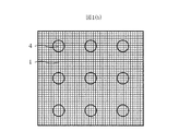
- FIGS. 1A and 1B are a first top view and a cross-sectional view of a tapered nanopillar solar cell according to Example 1 of the present invention.
- the tapered nanopillar photovoltaic cell of Example 1 is a tapered nanopillar photovoltaic cell in which a tapered nanopillar 4 is formed on a substrate 1.
- FIG. 1 shows a structure in which the columnar portion 6 of the tapered nanopillar 4 is a cylinder, as described above, the columnar portion 6 may be a columnar structure having a different cross-sectional shape such as a rectangular column. Good.
- the tapered nanopillar 4 includes an upper taper 5, a columnar portion 6, and a lower taper 7.
- the lower taper 7 is not an essential component, and the nanopillar 4 may be composed of only the upper taper 5 and the columnar portion 6. However, it is difficult for the manufacturing process to make the lower part of the nanopillar completely columnar, and the lower taper 7 may be formed.
- the nanopillar 4 in Example 1 includes those in which the lower taper 7 is formed and those in which the lower taper 7 is not formed in the technical scope thereof.
- FIG. 1B does not show the cross-sectional shapes of the upper taper 5 and the lower taper 7, but these can take various cross-sectional shapes such as a cylinder and a prism as well as the columnar portion 6.
- the dimensions characterizing the tapered nanopillar solar cell of the present invention are the diameter DT of the top of the upper taper 5, the diameter D of the columnar portion 6, the height HT of the upper taper 5, There are four types of height H of the tapered nanopillar 4. The influence of these four types of dimensions on the optical properties of the tapered nanopillar 4 will be described later.
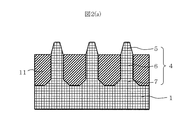
- 2 (a) and 2 (b) are a second top view and a cross-sectional view of a tapered nanopillar solar cell according to Example 1 of the present invention.
- the difference from the first top view and the cross-sectional view described above is that the insulating film 11 is formed on the side portions of the columnar portion 6 and the lower taper 7.
- the reason why it is desirable to form the insulating film 11 is as follows.
- a sealing material is provided around the cell. If there are fine irregularities such as a nanopillar array structure on the cell surface, it is difficult for the encapsulant to fill the area between the nanopillars. There is a possibility of becoming. In this case, the expansion and compression of the air are repeated due to the temperature change when the solar cell is operated, which may cause defects such as peeling of the sealing material. Therefore, prior to modularization, it is desirable from the viewpoint of preventing defects to fill the region between the nanopillars with some material.
- the region between the nanopillars is filled with the insulating film 11.
- the insulating film 11 is used as a protective film when the upper taper 5 is formed. Therefore, as described above, the insulating film 11 has both the role of a filler for preventing defects and the role of a protective film when manufacturing solar cells. Thereby, the man-hours and cost required for forming the insulating film 11 can be reduced.
- the material which comprises the nano pillar solar cell with a taper of Example 1 is described.
- the material of the substrate 1 and the tapered nanopillar 4 that are light absorption layers are semiconductors such as Si, CdTe, CuInGaSe, InP, GaAs, and Ge, and these are various such as single crystal, polycrystal, microcrystal, and amorphous. It can take the structure of Hereinafter, in Example 1, although the case where the material of the upper taper 5, the columnar part 6, and the lower taper 7 which comprise the taper nanopillar 4 is all the same is described, these may differ from each other.
- the material of the insulating film 11 is an insulator such as SiO 2 , SiN (silicon nitride), amorphous Si, SiC (silicon carbide), CdS, or a laminated structure of these insulators.
- the tapered nanopillar solar cell of Example 1 it is possible to achieve both suppression of an increase in reflectance when light is incident on the solar cell obliquely and light confinement between the nanopillars. .
- this effect will be described with reference to FIGS. 3 and 4 show the light absorption rate as an index of the above effect.
- the definition of optical absorptance is "[(light absorption inside tapered nanopillar 4) / (volume of tapered nanopillar 4)] / [(light absorption inside tapered nanopillar) / (taperless nanopillar Volume)] ”.
- the light absorption amount is “incident light amount ⁇ reflected light amount ⁇ transmitted light amount”.
- the suppression of the increase in reflectance increases the amount of light absorption by reducing the amount of reflected light.
- light confinement increases the amount of light absorption by reducing the amount of transmitted light. Therefore, the larger the light absorption amount, the higher the effect.
- the refractive index of the region from the light source to the nanopillar and the region between the nanopillars is 1.45. This numerical value is defined on the assumption that the region from the light source to the nanopillar and the region between the nanopillars are filled with SiO 2 as a sealing material or an insulating film, and the wavelength of the above material in the visible light region. This is because the refractive index of each is about 1.45.
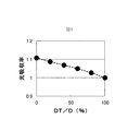
- FIG. 3 shows the calculation result of the light absorption rate when the DT / D of the tapered nanopillar 4 is changed.
- D 40 nm
- H 200 nm
- HT 60 nm
- the arrangement period of the nanopillars is 80 nm.
- the light absorption rate increases monotonously from 1. This means that as long as the upper taper 5 having a larger taper angle than the columnar portion 6 is provided, at least the effect of the present invention is achieved.
- the effect of the present invention can be further enhanced by changing the shape of the upper taper 5 from a columnar shape to a cone shape, that is, by increasing the taper angle of the upper taper 5.
- the solar cell according to Example 1 includes at least the substrate 1 and the plurality of pillars 4 provided on the surface of the substrate, and each of the plurality of pillars 4 includes the columnar portion 6 and the columnar portion 6. And an upper taper 5 provided at the tip of the upper taper 5.
- the taper angle of the upper taper 5 is larger than the taper angle of the columnar section 6.
- the taper angle is compared between the upper taper 5 and the columnar part 6 only. That is, as described above, when the nanopillar 4 is manufactured, the lower taper 7 may be formed, and this region may have a taper angle larger than that of the upper taper 5.
- the lower taper 7 which is an exceptionally large taper angle is omitted, and the taper angle is compared only between the upper taper 5 and the columnar portion 6. Assumed to be performed. This is based on the fact that DT is a parameter defined by the shape of the upper taper 5, and D is a parameter defined by the shape of the columnar portion 6 (not the lower taper 7).
- FIG. 4 is a calculation result of the light absorption rate when the HT / H of the tapered nanopillar 4 is changed.
- D 40 nm
- DT 16 nm
- H 200 nm
- the arrangement period of the nanopillars is 80 nm.
- the shape of the upper taper 5 satisfies the condition of 0% ⁇ HT / H ⁇ 60%, that is, the height of the upper taper 5 is the height of the pillar 4. It can be seen that it is desirable to be larger than 0% and smaller than 60%.
- the definition of the nanopillar array structure is a columnar structure having a width equal to or finer than the wavelength of sunlight, and thus it is desirable that D ⁇ 1 ⁇ m.
- the uneven shape of the nanopillar array structure brings about wave optical effects such as interference and diffraction, and as a result, an excellent antireflection effect is realized.
- the pillar diameter is larger than the above range, the incident light behaves geometrically and the antireflection effect is reduced.
- Example 1 the same effect can be expected when a tapered nanohole solar cell or a tapered nanogroove solar cell is used instead of the tapered nanopillar solar cell.
- tapered nanopillar solar cells are taken up in the present specification, but similarly, tapered nanohole solar cells or tapered nanogroove solar cells may be used.
- FIG. 5 is a diagram illustrating a method of manufacturing the tapered nanopillar solar cell of Example 1. Hereinafter, based on FIG. 5, the manufacturing method of the photovoltaic cell of this invention is demonstrated.
- an etching mask 21 is formed on the surface of the substrate 1.
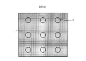
- a cross-sectional view of the structure after formation is shown in FIG. 5A, and a top view is shown in FIG. 5B.
- the etching mask 21 serves as a mask for the etching process in the next process, and as its material, metal nanoparticles, SiO 2 , resist, or the like is generally used.
- the etching mask 21 can be formed by self-organization by dispersing the nanoparticles.
- the etching mask 21 may be formed by processing a metal by a method such as lift-off or etching.
- SiO 2 or a resist is used, the etching mask 21 can be formed by patterning using lithography.
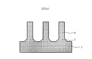
- the columnar portion 6 and the lower taper 7 of the tapered nanopillar 4 are formed by processing the surface of the substrate 1.
- a cross-sectional view of the structure after formation is shown in FIG. 5C, and a top view is shown in FIG. 5D.
- the columnar portion 6 and the lower taper 7 are formed by a method such as dry etching, wet etching, or laser ablation. From the viewpoint of the antireflection effect, it is desirable that the aspect ratio of the tapered nanopillar 4, that is, the value of “height / diameter” is large.
- the columnar portion is formed by using dry etching with high processing anisotropy. 6 and a lower taper 7 are preferably formed. In order to increase the aspect ratio, it is also an effective method to make the etching mask 21 have a laminated structure of two or more layers.
- the etching mask 21 is removed.
- a sectional view of the structure after removal is shown in FIG. 5 (e), and a top view is shown in FIG. 5 (f).
- the etching mask 21 is removed by a method such as wet etching or ashing.
- the insulating film 11 is formed.
- a sectional view of the structure after the formation is shown in FIG. 5G, and a top view is shown in FIG.
- the insulating film 11 is formed by a film forming method such as a CVD method, a sputtering method, an epitaxy method, or a vapor deposition method.
- the insulating film 11 is not formed on the side portion of the columnar portion 6 that will later become the upper taper 5.
- the insulating film 11 is formed to a position higher than the top of the columnar portion 6, and then CMP (Chemical Mechanical Polishing), It is effective to reduce the film thickness of the insulating film 11 by dry etching, wet etching, or a combination thereof.
- CMP Chemical Mechanical Polishing
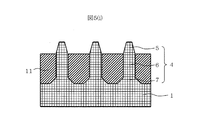
- the upper taper 5 is formed.
- a sectional view of the structure after the formation is shown in FIG. 5 (i), and a top view is shown in FIG. 5 (j).
- the upper taper 5 is formed by processing the top of the columnar portion 6 by wet etching or dry etching.
- wet etching using a highly anisotropic etching solution is effective.
- the insulating film 11 serves as a protective film, so that the columnar portion 6 and the lower taper 7 are prevented from being etched. In that respect, it is desirable for the etching solution that the etching rate for the upper taper 5 is faster than the etching rate for the insulating film 11.
- the above is the manufacturing method of the solar battery cell in the first embodiment.
- heat treatment, plasma treatment, etc. may be added as appropriate to improve the crystallinity and film quality of each film or to improve the quality of the interface with the adjacent film.
- FIG. 6B two of the insulating film 11 and the transparent conductive oxide 13 are not shown.
- the structure of the first embodiment defines only the shape of the tapered nanopillar 4 whereas the substrate 1 and the columnar portion 6 are p-type semiconductors in the structure of the second embodiment.
- an emitter layer 12 that is an n-type semiconductor layer and has an impurity concentration higher than that of the columnar portion 6 is provided, and a pn junction is formed at the interface between the columnar portion 6 and the emitter layer 12 (implementation).
- the lower taper 7 is not essential, but if provided, it is a p-type semiconductor).
- a transparent conductive oxide 13 is provided on the emitter layer 12 as a surface electrode.
- FIG. 6 shows a structure in which the boundary surface between the columnar portion 6 and the emitter layer 12 is on the same plane as the boundary surface between the insulating film 11 and the transparent conductive oxide 13. 6 and the transparent conductive oxide 13 are in contact with each other, the leakage current increases and the characteristics of the solar battery cell are degraded. Therefore, the boundary surface between the columnar portion 6 and the emitter layer 12 is formed between the insulating film 11 and the transparent conductive oxide.
- the transparent conductive oxide 13 is an oxide containing an element such as In, Zn, Sn, or Ga and a composite oxide thereof, and an additive such as fluorine may be added thereto.
- the conventional nanopillar solar cell structure has recombination loss due to the emitter layer being provided in the nanopillar region where optical confinement occurs, and series resistance due to the use of a transparent conductive oxide as the surface electrode.
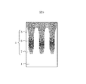
- FIG. 9 shows the result of calculating the light intensity distribution when light enters the tapered nanopillar array structure by the FDTD method.
- the darker black region has higher light intensity, and conversely, the white region has lower light intensity.
- the light intensity distribution inside the substrate 1 and the tapered nanopillar 4 is not shown, and these regions are displayed in white. From FIG. 9, it can be seen that in the tapered nanopillar array structure, similarly to the nanopillar array structure, the light intensity is high in the region between the adjacent tapered nanopillars 4.
- the light intensity at the side portion of the columnar portion 6 is higher than the side portions of the upper taper 5 and the lower taper 7. Therefore, in the tapered nanopillar array structure, light confinement mainly occurs in the region between the columnar portions 6, and the light confinement in the region between the upper taper 5 and the region between the lower taper 7 is relatively small. It can be said that it is weak.
- the emitter layer in order to reduce recombination loss in the emitter layer, is not the columnar portion 6 but the upper taper 5 or the lower taper 7 in the tapered nanopillar 4. It can be seen that it is desirable to provide it.
- the substrate 1 and the columnar part 6 are of the first conductivity type (p-type), and the upper taper 5 is of the first conductivity type.
- the second conductivity types n-type
- Example 2 There are two methods for manufacturing the structure of Example 2, depending on whether the emitter layer 12 is formed before or after the tapered nanopillar 4 is formed.
- As the former method there is a method in which the emitter layer 12 is formed on the entire surface of the substrate 1 before the steps shown in FIGS.
- the emitter layer 12 is formed by an impurity implantation method such as a vapor phase diffusion method, a solid phase diffusion method, or an ion implantation method, or a film formation method.
- the structure of Example 2 can be manufactured by the same manufacturing method as that of Example 1.
- the upper taper 5 is formed after the steps shown in FIGS. There is a method of implanting impurities.
- the transparent conductive oxide 13 is formed by sputtering, CVD, coating, printing, or the like.
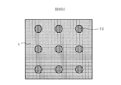
- FIG. 7A and 7B are a cross-sectional view and a top view of the solar battery cell according to Example 3 of the present invention.
- the insulating film 11 is not shown.
- this is a kind of structure in which the emitter layer 12 is provided on the tapered nanopillar 4.
- the emitter layer 12 is provided on the upper taper 5 in the structure of the second embodiment, whereas the emitter layer 12 is formed on the lower taper 7 and a part of the substrate 1 in the structure of the third embodiment.
- a pattern electrode can be used instead of the transparent conductive oxide 13 as a surface electrode.
- the sheet resistance of the emitter layer 12 can be reduced by increasing the thickness of the region of the emitter layer 12 provided on the substrate 1. Specifically, it is desirable that the thickness of the entire emitter layer 12, that is, the thickness of the combined region of the lower taper 7 and part of the substrate 1 is 500 nm or more.
- the emitter layer 12 is continuous over the entire surface of the substrate 1 without being isolated from each other.
- the emitter layer 12 is not necessary to use an electrode formed on the entire surface in order to collect carriers from the emitter layer 12, Ag, It becomes possible to use pattern electrodes made of Al, Ti, Pd, Ni, Cu, or a laminated structure thereof.
- the pattern electrode is provided at a position in contact with the emitter layer 12. It is desirable not to form the tapered nanopillar 4 in the region where the pattern electrode is formed.
- the solar cell according to Example 3 includes a first conductivity type (p-type) substrate 1, a plurality of first conductivity type (p-type) pillars 4 provided on the surface of the substrate 1, An emitter layer 12 of a second conductivity type (n-type) different from the first conductivity type provided between the plurality of pillars 4 on the surface of the substrate 1, and at least a part (lower part) of the emitter layer A region having a larger taper angle than the pillar 4 is present in the region corresponding to the taper 7.
- the emitter layer 12 may be formed after the steps shown in FIGS. 5C and 5D in the manufacturing method of the structure of Example 1.
- the emitter layer 12 is formed by an anisotropic impurity implantation method such as an ion implantation method.
- an anisotropic impurity implantation method such as an ion implantation method.
- the etching mask 21 as a mask for impurity implantation, man-hours and costs can be reduced.
- the reason why the anisotropic impurity implantation method is used is that when the impurity implantation is performed by the isotropic implantation method, the emitter layer 12 is also formed on the side wall portion of the columnar portion 6.
- the emitter layer 12 is also formed below the tapered nanopillar 4. It is desirable to suppress diffusion by lowering or shortening the activation heat treatment so that the substrate 1 and the tapered nanopillar 4 are not separated by the emitter layer 12.
Landscapes
- Photovoltaic Devices (AREA)
Abstract
太陽電池セルにおいて、基板(1)と、基板の表面に設けられる複数のピラー(4)と、を設け、複数のピラーのそれぞれにおいて、柱状部(6)と、柱状部の先端に設けられる上部テーパー(5)と、を設け、上部テーパーのテーパー角を、柱状部のテーパー角よりも大きい構造とする。係る構成によって、第一に、光の入射角増大に伴う反射率増大抑制と光閉じ込めとの両立を実現することのできる太陽電池セルを実現することができる。第二に、再結合損失低減と、表面電極としてパターン電極を用いることとを両立することができる。
Description
本発明は太陽電池セルに関する。
現在、太陽電池セルの表面反射防止構造としては、アルカリ溶液または酸溶液によるウェットエッチングで形成されたテクスチャ構造が、最も一般的に用いられている。これに対して、太陽光の波長と同等またはより微細なサイズの凹凸が周期的に形成された構造(いわゆるサブ波長構造)を表面反射防止構造に用いることで、より低い反射率が実現されることが知られている。そのため、サブ波長構造を太陽電池セルの表面反射防止構造として用いることで、従来よりも反射率を低減し、出力電流を増大することが可能であると期待されている。例えば、非特許文献1では、サブ波長構造の中でも、後述するナノピラーアレイ構造を表面反射防止構造として用いることで、従来構造の太陽電池セルと比較して、反射防止効果による出力電流増大が可能であることが、シミュレーションにより示されている。
上述のシミュレーションは、太陽電池セルの表面に対して、光が垂直入射した場合の反射防止に関するものであるが、一般的に、屋外に設置された太陽光パネルが発電する状況においては、太陽電池セルの表面に対して、光が垂直入射することは稀であり、ある入射角をもって、光が斜めに入射するのが通常である。従って、太陽光パネルの発電特性向上のためには、太陽電池セルの表面に対して、光が斜めに入射した場合の反射率増大を抑制することが必要である。例えば、非特許文献2では、後述するナノピラーアレイ構造とナノコーンアレイ構造とに対して、反射率の入射角依存性を、シミュレーションでそれぞれ調べた結果が示されている。それによると、ナノピラーアレイ構造よりもナノコーンアレイ構造の方が、入射角の増大に伴う反射率の増大が抑制される。以下、入射角は、太陽電池セル表面の法線ベクトルと、光の進行方向とのなす角度で定義する。従って、例えば、光が太陽電池セル表面に垂直入射する場合、入射角は0°とする。
次に、サブ波長構造を用いた太陽電池セルの構造について、後述するナノピラー太陽電池セルを例にとって述べる。現在までに提案および研究されている、ナノピラー太陽電池セルの構造は3種類に分類される。それら3種類とは、非特許文献1の表2に示されている、Nanowire Solar Cell(subsurface-junction)、Nanowire Solar Cell(planar-junction)、および、Nanowire Solar Cell(radial-junction)である。ここでのNanowireは、本明細書におけるナノピラーと同義である。以下、本明細書では、Nanowire Solar Cell(subsurface-junction)を、planar深接合型ナノピラー太陽電池セル、Nanowire Solar Cell(planar-junction)を、planar浅接合型ナノピラー太陽電池セル、Nanowire Solar Cell(radial-junction)を、radial接合型ナノピラー太陽電池セルとそれぞれ記す。
ここで、上述した3種類の太陽電池セルには、p型基板の表面に不純物が高濃度にドーピングされたn+層が形成されることにより、pn接合が形成されている(pとnは逆でも良い)。以下、「不純物が高濃度にドーピングされた層」のことを「エミッタ層」と記す。エミッタ層の役割は主に、pn接合のポテンシャル差を形成して電子と正孔とを分離させる役割、エミッタ層に収集されたキャリアが電極に到達するまでの伝導経路としての役割、および、電極との接触抵抗を低減する役割、の3点である。planar深接合型ナノピラー太陽電池セルと、planar浅接合型ナノピラー太陽電池セルにおいては、pn接合面は、基板表面に平行な平面状に形成される。一方、radial接合型ナノピラー太陽電池セルにおいては、pn接合面は、ナノピラー表面と平行に形成される。
ここで、上述の3種類の太陽電池セルの違いは、ナノピラー内におけるエミッタ層の位置にある。planar深接合型ナノピラー太陽電池セルにおいては、エミッタ層は、ナノピラーの全領域に存在している。これに対し、planar浅接合型ナノピラー太陽電池セルにおいては、エミッタ層は、ナノピラーの頂部に存在している。また、radial接合型ナノピラー太陽電池セルにおいては、エミッタ層は、ナノピラーの側壁部分に存在している。以上のように、ナノピラー内におけるエミッタ層の位置は異なるものの、従来のナノピラー太陽電池セル構造のいずれにおいても、ナノピラーの少なくとも一部の領域にエミッタ層が存在する点は共通である。
また、非特許文献3には、ナノピラー太陽電池セルにおけるキャリア発生率分布をシミュレーションにより調べた結果が記載されており、ナノピラー内部でのキャリア発生率が、その直下の基板でのキャリア発生率に比べて2桁から3桁程度高いということが示されている。
IEEE IEDM Technical Digest, pp. 856 - 859 (2011).
Journal of Applied Physics, vol. 100, 124504 (2006).
IEEE IEDM Technical Digest, pp. 704 - 707 (2010).
<光閉じ込めについて>
上述した通り、ナノコーンアレイ構造は、ナノピラーアレイ構造と比べて、光の入射角増大に伴う反射率増大が抑制されるという利点がある。一方で、ナノコーンアレイ構造には、ナノピラーアレイ構造と比べて、光閉じ込め特性が劣るという課題がある。以下、この課題について述べる。
上述した通り、ナノコーンアレイ構造は、ナノピラーアレイ構造と比べて、光の入射角増大に伴う反射率増大が抑制されるという利点がある。一方で、ナノコーンアレイ構造には、ナノピラーアレイ構造と比べて、光閉じ込め特性が劣るという課題がある。以下、この課題について述べる。
図8(a)および(b)は、本発明に先立って、発明者によりなされた検討の結果であり、ナノピラーアレイ構造とナノコーンアレイ構造に光が入射したときの光強度分布を、FDTD法(Finite Differential Time Domain method)により、それぞれ計算した結果である。図8(a)には、基板1上に、直径40nm、高さ200nmのナノピラー2が、周期80nmで配列されたナノピラーアレイ構造が示されている。一方、図8(b)には、基板1上に、底辺80nm、高さ200nmのナノコーン3が、周期80nmで配列されたナノコーンアレイ構造が示されている。図8(a)および(b)において、濃い黒色の領域ほど、光強度が高く、逆に白色の領域は、光強度が低い。なお、基板1、ナノピラー2、およびナノコーン3内部の光強度分布は図示されておらず、これらの領域は白色で表示されている。図8(a)から、ナノピラーアレイ構造においては、隣接するナノピラー2の間の領域で、光強度が高いことがわかる。これは、ナノピラーアレイ構造が、優れた光閉じ込め特性を有することを意味する。一方で、図8(b)に示したナノコーンアレイ構造では、隣接するナノコーン3の間の領域での光強度は、ナノピラーアレイ構造の場合と比べて低い。この結果から、光閉じ込め特性の点では、ナノコーンアレイ構造はナノピラーアレイ構造に劣るということがわかる。
<再結合損失について>
上述した通り、エミッタ層には太陽電池セルにとって有用な役割があるため、エミッタ層を設けること自体は必要である。しかしながら、従来の3種類の太陽電池セルにおいては、ナノピラー内にエミッタ層が存在するため、再結合損失が大きいという課題が存在する。以下、ナノピラー太陽電池セルを例にとり、この課題について述べる。
上述した通り、エミッタ層には太陽電池セルにとって有用な役割があるため、エミッタ層を設けること自体は必要である。しかしながら、従来の3種類の太陽電池セルにおいては、ナノピラー内にエミッタ層が存在するため、再結合損失が大きいという課題が存在する。以下、ナノピラー太陽電池セルを例にとり、この課題について述べる。
図8(a)に示したように、ナノピラーアレイ構造においては、隣接するナノピラー2の間の領域で、光強度が高い。この結果、ナノピラー2の内部でのキャリア発生率は、基板でのキャリア発生率に比べて高くなる。それだけでなく、図8(a)から、ナノピラー2の内部の中でも、側壁部でのキャリア発生率が特に高いということもわかる。
ここで、高濃度にドーピングされた半導体では、種々の再結合過程のうち、オージェ再結合の確率が高くなることが知られている。また、オージェ再結合の寿命も、不純物濃度の増大に伴って短くなる。このため、高濃度にドーピングされた半導体で光吸収が起こり、電子正孔対が発生しても、それらのキャリアは、短時間のうちにオージェ再結合によって消滅する確率が高い。従って、ナノピラー内にエミッタ層が存在する太陽電池セルにおいてはオージェ再結合に起因する損失が課題となる。
従来の3種類のナノピラー太陽電池セル構造のうち、planar深接合型ナノピラー太陽電池セルでは、他の2種類の構造よりもエミッタ層の占める体積が大きいことから、再結合損失が最も大きい。それに比べれば、planar浅接合型ナノピラー太陽電池セルと、radial接合型ナノピラー太陽電池セルでは、エミッタ層を薄膜化しているために、再結合損失は比較的小さいが、それでも、ナノピラーの少なくとも一部の領域に、高濃度にドーピングされたエミッタ層が存在することによる再結合損失は避けられない。また、上述のように、図8(a)によれば、ナノピラー2の側壁部でのキャリア発生率が特に高い。このことから、radial接合型ナノピラー太陽電池セルにおいては、エミッタ層を薄膜化しているとはいえ、全ての側壁部が高濃度にドーピングされることによって、再結合損失が大きくなっていることが懸念される。
<表面電極について>
従来の太陽電池セルの別の課題として、表面電極に関する課題について述べる。planar深接合型ナノピラー太陽電池セルにおいては、エミッタ層が連続した層からなるため、表面電極をエミッタ層のいずれの領域に設けても、エミッタ層全体からのキャリアを表面電極に到達させることができる。そのため、表面電極を、ナノピラーとは別の領域に設けることが可能である。従って、表面電極は、結晶Si太陽電池セルで一般的に用いられている、AgやAlといった透明でない金属からなるフィンガー・バスバーパターンの電極でもよいし、薄膜太陽電池セルで用いられている、ITO(In-Sn-O)などの透明導電性酸化物を全面に形成した電極でもよい。
従来の太陽電池セルの別の課題として、表面電極に関する課題について述べる。planar深接合型ナノピラー太陽電池セルにおいては、エミッタ層が連続した層からなるため、表面電極をエミッタ層のいずれの領域に設けても、エミッタ層全体からのキャリアを表面電極に到達させることができる。そのため、表面電極を、ナノピラーとは別の領域に設けることが可能である。従って、表面電極は、結晶Si太陽電池セルで一般的に用いられている、AgやAlといった透明でない金属からなるフィンガー・バスバーパターンの電極でもよいし、薄膜太陽電池セルで用いられている、ITO(In-Sn-O)などの透明導電性酸化物を全面に形成した電極でもよい。
一方、planar浅接合型ナノピラー太陽電池セルとradial接合型ナノピラー太陽電池セルにおいては、表面電極として、フィンガー・バスバーパターンの電極を用いることができず、全面に形成された電極を用いる必要があり、その結果、電極の材料がITOなどの透明導電性酸化物に限定される。その理由は以下の通りである。まず、planar浅接合型ナノピラー太陽電池セルの場合には、ナノピラーの頂部にのみエミッタ層が形成されているため、異なるナノピラー内のエミッタ層は互いに孤立して存在する。従って、これらエミッタ層からキャリアを収集するためには、孤立した複数のエミッタ層のそれぞれと電気的に接続された電極が必要となるため、パターン電極ではなく全面に形成された電極を用いる必要がある。また、radial接合型ナノピラー太陽電池セルの場合には、上述のように、エミッタ層を薄膜化しているために、エミッタ層のシート抵抗が高く、その結果、パターン電極を用いると、直列抵抗損失が大きくなるため、表面電極としては、全面に形成された電極を用いる必要がある。
以上2つのセルのように、全面に電極を形成せざるを得ないセル構造の場合には、ナノピラー上部も電極で覆われることになるため、太陽光を反射してしまうAg、Al等の金属を表面電極として用いることはできない。よって、表面電極の材料は透明導電性酸化物に限定される。
表面電極としてITOなどの透明導電性酸化物を用いると、エミッタ層と透明導電性酸化物との接触抵抗、および、透明導電性酸化物の光吸収に起因する損失が発生する。
まず接触抵抗について述べる。パターン電極の材料として一般的に用いられるAgやAlといった金属と比べると、ITOなどの透明導電性酸化物は、Siをはじめとする半導体材料との接触抵抗が高い。一般的に、接触抵抗は、半導体の表面不純物濃度を高くすることで低減することが可能だが、上述のように、太陽電池セルにおいて、表面不純物濃度を高くすることは、再結合損失の増大をもたらすため、接触抵抗低減のために表面不純物濃度を任意に高くすることはできない。従って、透明導電性酸化物を表面電極として用いると、高い接触抵抗による損失と、再結合損失の両方を同時に回避することが困難である。
また、透明導電性酸化物は、一般的に、紫外光や赤外光を吸収することが知られており、それを表面電極として用いると、太陽電池セルの光吸収層に到達する光量が低減するという損失が発生する。以上のことから、表面電極としてITOなどの透明導電性酸化物を用いると、太陽電池セルの特性低下をもたらす要因となる。
以上をまとめると、サブ波長構造、特にナノピラーアレイ構造を、表面反射防止構造として用いる、従来の太陽電池セルの課題は以下の通りである。第一に、光の入射角増大に伴う反射率増大抑制と、光閉じ込めとの両立が困難であるという課題が存在する。第二に、ナノピラー内部に高濃度にドーピングされたエミッタ層が存在する太陽電池セルにおいては、再結合損失が大きいという課題が存在する。第三に、エミッタ層が互いに孤立した太陽電池セルや、エミッタ層を薄膜化した太陽電池セルにおいては、表面電極として、パターン電極を用いることができず、ITOなどの透明導電性酸化物を全面に形成した電極を用いる必要があり、この結果、エミッタ層と透明導電性酸化物との接触抵抗、および、透明導電性酸化物の光吸収に起因する損失が発生する。サブ波長構造を有する太陽電池セルにおいて、上記3つの課題を解決する手法は、従来はなかった。
本発明は、かかる事情を鑑みてなされたものであり、第一に、光の入射角増大に伴う反射率増大抑制と光閉じ込めとの両立を実現することのできる太陽電池セルを実現することを目的とする。第二に、サブ波長構造内部での再結合損失低減と、表面電極としてパターン電極を用いることとを両立することのできる太陽電池セルを実現することを目的とする。本発明の前記ならびにその他の目的と新規な特徴は、本明細書の記述および添付図面から明らかになるであろう。
本願において開示される発明のうち代表的なものを簡単に説明すれば、次のとおりである。
第1に、太陽電池セルであって、基板と、基板の表面に設けられる複数のピラーと、を有し、複数のピラーのそれぞれは、柱状部と、柱状部の先端に設けられる上部テーパーと、を具備し、上部テーパーのテーパー角は、柱状部のテーパー角よりも大きいことを特徴とする。
第2に、太陽電池セルであって、第1導電型の基板と、基板の表面に設けられ、第1導電型の複数のピラーと、基板の表面のうち複数のピラーの間に設けられ、第1導電型とは異なる第2導電型のエミッタ層と、を有し、エミッタ層の少なくとも一部に、ピラーよりもテーパー角の大きい領域があることを特徴とする。
本発明によると、第一に、光の入射角増大に伴う反射率増大抑制と光閉じ込めとの両立を実現することのできる太陽電池セルを実現することができる。第二に、再結合損失低減と、表面電極としてパターン電極を用いることとを両立することができる。
<用語の定義>
本明細書では、サブ波長構造の中でも、ナノピラーアレイ構造、ナノコーンアレイ構造、ナノホールアレイ構造、ナノグルーブアレイ構造、テーパー付きナノピラーアレイ構造、テーパー付きナノホールアレイ構造、およびテーパー付きナノグルーブアレイ構造、の7種類の構造を取り上げる。以下、これら7種類の構造の定義を述べる。ナノピラーアレイ構造とは、太陽光の波長と同等、またはより微細な幅を有する柱状構造(以下、「ナノピラー」または単に「ピラー」と記す)が、基板表面に周期的に配列された構造である。当該柱状構造の柱軸方向は基板面と垂直である。以下の実施例ではナノピラーの例として円柱を挙げているが、角柱など、異なる断面形状であってもよい。ナノコーンアレイ構造とは、太陽光の波長と同等、またはより微細な底辺を有する錐状構造が、基板表面に周期的に配列された構造である。当該錐状構造の錐軸方向は基板面と垂直である。以下の実施例ではナノコーンの例として円錐を挙げているが、角錐など、異なる断面形状であってもよい。ナノホールアレイ構造とは、太陽光の波長と同等、またはより微細な幅の柱状構造を為す空隙が、基板表面に周期的にあけられた構造である。当該柱状構造の柱軸方向は基板面と垂直である。同様に、柱状構造の形状は、円柱でなく、角柱など、異なる断面形状であってもよい。ナノグルーブアレイ構造とは、太陽光の波長と同等、またはより微細な幅を有する凸部が基板表面上に周期的に配列され、その結果、凸部の間に周期的な溝(グルーブ)を持つ構造である。凸部の断面形状としては、四角形、三角形、あるいは扇型などが一般的である。基板の上面から観察した場合、ナノピラーアレイ構造とナノホールアレイ構造が、2次元的な周期性を有する構造であるのに対して、ナノグルーブアレイ構造は、1次元的な周期性を有する構造である。なお、柱状構造、および凸部の「幅」を、基板面に平行な方向における長さとする。テーパー付きナノピラーアレイ構造とは、ナノピラーアレイ構造において、ナノピラーの頂部、底部、あるいはその両方に、錐状の傾斜形状(テーパー)が存在する構造である。以下の実施例では、テーパーの例として円錐状の傾斜形状を挙げているが、角錐状など、異なる断面形状であってもよい。テーパー付きナノホールアレイ構造とは、ナノホールアレイ構造において、ナノホールの頂部、底部、あるいはその両方に、錐状の傾斜形状(テーパー)が存在する構造である。以下の実施例では、テーパーの例として円錐状の傾斜形状を挙げているが、角錐状など、異なる断面形状であってもよい。テーパー付きナノグルーブアレイ構造とは、ナノグルーブアレイ構造において、凸部の頂部、底部、あるいはその両方に、錐状の傾斜形状(テーパー)が存在する構造である。テーパーの断面形状は、角錐状など、任意の形状でよい。
本明細書では、サブ波長構造の中でも、ナノピラーアレイ構造、ナノコーンアレイ構造、ナノホールアレイ構造、ナノグルーブアレイ構造、テーパー付きナノピラーアレイ構造、テーパー付きナノホールアレイ構造、およびテーパー付きナノグルーブアレイ構造、の7種類の構造を取り上げる。以下、これら7種類の構造の定義を述べる。ナノピラーアレイ構造とは、太陽光の波長と同等、またはより微細な幅を有する柱状構造(以下、「ナノピラー」または単に「ピラー」と記す)が、基板表面に周期的に配列された構造である。当該柱状構造の柱軸方向は基板面と垂直である。以下の実施例ではナノピラーの例として円柱を挙げているが、角柱など、異なる断面形状であってもよい。ナノコーンアレイ構造とは、太陽光の波長と同等、またはより微細な底辺を有する錐状構造が、基板表面に周期的に配列された構造である。当該錐状構造の錐軸方向は基板面と垂直である。以下の実施例ではナノコーンの例として円錐を挙げているが、角錐など、異なる断面形状であってもよい。ナノホールアレイ構造とは、太陽光の波長と同等、またはより微細な幅の柱状構造を為す空隙が、基板表面に周期的にあけられた構造である。当該柱状構造の柱軸方向は基板面と垂直である。同様に、柱状構造の形状は、円柱でなく、角柱など、異なる断面形状であってもよい。ナノグルーブアレイ構造とは、太陽光の波長と同等、またはより微細な幅を有する凸部が基板表面上に周期的に配列され、その結果、凸部の間に周期的な溝(グルーブ)を持つ構造である。凸部の断面形状としては、四角形、三角形、あるいは扇型などが一般的である。基板の上面から観察した場合、ナノピラーアレイ構造とナノホールアレイ構造が、2次元的な周期性を有する構造であるのに対して、ナノグルーブアレイ構造は、1次元的な周期性を有する構造である。なお、柱状構造、および凸部の「幅」を、基板面に平行な方向における長さとする。テーパー付きナノピラーアレイ構造とは、ナノピラーアレイ構造において、ナノピラーの頂部、底部、あるいはその両方に、錐状の傾斜形状(テーパー)が存在する構造である。以下の実施例では、テーパーの例として円錐状の傾斜形状を挙げているが、角錐状など、異なる断面形状であってもよい。テーパー付きナノホールアレイ構造とは、ナノホールアレイ構造において、ナノホールの頂部、底部、あるいはその両方に、錐状の傾斜形状(テーパー)が存在する構造である。以下の実施例では、テーパーの例として円錐状の傾斜形状を挙げているが、角錐状など、異なる断面形状であってもよい。テーパー付きナノグルーブアレイ構造とは、ナノグルーブアレイ構造において、凸部の頂部、底部、あるいはその両方に、錐状の傾斜形状(テーパー)が存在する構造である。テーパーの断面形状は、角錐状など、任意の形状でよい。
これら7種類のサブ波長構造の反射防止効果について述べると、ナノピラーアレイ構造、ナノコーンアレイ構造、ナノホールアレイ構造、テーパー付きナノピラーアレイ構造、および、テーパー付きナノホールアレイ構造、の反射率は、一般的に、ほぼ同程度であり、ナノグルーブアレイ構造およびテーパー付きナノグルーブアレイ構造、は、前記3種類の構造と比較すると、一般的に、反射率は高いという違いがあるものの、以下で述べるように、いずれも本発明の対象となる。本明細書では、ナノピラーアレイ構造、ナノコーンアレイ構造、ナノホールアレイ構造、ナノグルーブアレイ構造、テーパー付きナノピラーアレイ構造、テーパー付きナノホールアレイ構造、テーパー付きナノグルーブアレイ構造、を、表面反射防止構造として有する太陽電池セルを、それぞれ、ナノピラー太陽電池セル、ナノコーン太陽電池セル、ナノホール太陽電池セル、ナノグルーブ太陽電池セル、テーパー付きナノピラー太陽電池セル、テーパー付きナノホール太陽電池セル、テーパー付きナノグルーブ太陽電池セル、と記す。
なお、以下の実施例では、基板等をp型、エミッタ層をn型として説明しているが、これらの導電型を逆にしたものについても同様の議論が可能であり、本願発明の技術的範囲に属するものである。
<セル構造>
図1(a)および(b)は、本発明の実施例1に係るテーパー付きナノピラー太陽電池セルの第1の上面図および断面図である。実施例1のテーパー付きナノピラー太陽電池セルは、基板1上に、テーパー付きナノピラー4が形成されたテーパー付きナノピラー太陽電池セルである。図1には、テーパー付きナノピラー4の柱状部6が円柱である場合の構造が示されているが、上述の通り、柱状部6は、角柱など、異なる断面形状を有する柱状構造であってもよい。テーパー付きナノピラー4は、上部テーパー5と、柱状部6と、下部テーパー7とからなる。ここで、本実施例において、下部テーパー7は必須の構成要素ではなく、ナノピラー4を、上部テーパー5と、柱状部6のみから構成しても良い。但し、ナノピラーの下部を完全に柱状とすることは製造プロセス上困難であり、下部テーパー7が形成されてしまう場合もある。実施例1におけるナノピラー4は、係る下部テーパー7が形成されるものも形成されないものも、その技術的範囲に含むものである。
図1(a)および(b)は、本発明の実施例1に係るテーパー付きナノピラー太陽電池セルの第1の上面図および断面図である。実施例1のテーパー付きナノピラー太陽電池セルは、基板1上に、テーパー付きナノピラー4が形成されたテーパー付きナノピラー太陽電池セルである。図1には、テーパー付きナノピラー4の柱状部6が円柱である場合の構造が示されているが、上述の通り、柱状部6は、角柱など、異なる断面形状を有する柱状構造であってもよい。テーパー付きナノピラー4は、上部テーパー5と、柱状部6と、下部テーパー7とからなる。ここで、本実施例において、下部テーパー7は必須の構成要素ではなく、ナノピラー4を、上部テーパー5と、柱状部6のみから構成しても良い。但し、ナノピラーの下部を完全に柱状とすることは製造プロセス上困難であり、下部テーパー7が形成されてしまう場合もある。実施例1におけるナノピラー4は、係る下部テーパー7が形成されるものも形成されないものも、その技術的範囲に含むものである。
図1(b)には、上部テーパー5および下部テーパー7の断面形状を示していないが、これらはいずれも、柱状部6と同様に、円柱、角柱など、種々の断面形状をとり得る。本発明のテーパー付きナノピラー太陽電池セルを特徴づける寸法は、図1(a)に示したように、上部テーパー5の頂部の直径DT、柱状部6の直径D、上部テーパー5の高さHT、および、テーパー付きナノピラー4の高さHの4種類である。これら4種類の寸法が、テーパー付きナノピラー4の光学特性に与える影響については後述する。
図2(a)および(b)は、本発明の実施例1に係るテーパー付きナノピラー太陽電池セルの第2の上面図および断面図である。上述の、第1の上面図および断面図との違いは、柱状部6および下部テーパー7の側部に、絶縁膜11が形成されているということである。
絶縁膜11が形成されるのが望ましい理由は以下の通りである。一般的に、太陽電池セルをモジュール化する際には、セル周囲に封止材が設けられる。セル表面に、ナノピラーアレイ構造のような微細な凹凸が存在する場合には、封止材がナノピラー間の領域を充填することが困難であり、その結果、ナノピラー間の領域が空気のままでモジュール化される可能性がある。この場合、太陽電池を動作させる際の温度変化によって、空気の膨張および圧縮が繰り返され、そのことが、封止材の剥がれ等の不良を誘発する原因となり得る。従って、モジュール化に先立ち、ナノピラー間の領域を何らかの材料で充填することが、不良防止の観点から望ましい。ナノピラー間の領域を充填する材料には、自身は光を吸収せず、ナノピラーに光を吸収させるという性質が望まれるため、バンドギャップの大きい絶縁体を用いるのが良い。このため、本発明の太陽電池セルにおいては、絶縁膜11により、ナノピラー間の領域が充填される。
また、後述のように、実施例1のテーパー付きナノピラー太陽電池セルの製造方法において、上部テーパー5を形成する際の保護膜として絶縁膜11を用いる。従って、絶縁膜11は、上述のように、不良防止のための充填剤という役割と、太陽電池セル製造時の保護膜という役割とを兼ね備える。これにより、絶縁膜11の形成に要する工数やコストを低減することができる。
実施例1のテーパー付きナノピラー太陽電池セルを構成する材料について述べる。光吸収層である、基板1、および、テーパー付きナノピラー4の材料は、Si、CdTe、CuInGaSe、InP、GaAs、Geなどの半導体であり、これらは単結晶、多結晶、微結晶、アモルファスなど種々の構造をとりうる。以下、実施例1では、テーパー付きナノピラー4を構成する上部テーパー5、柱状部6、および下部テーパー7の材料が、いずれも同一である場合について述べるが、これらは互いに異なっていてもよい。絶縁膜11の材料は、SiO2、SiN(窒化シリコン)、アモルファスSi、SiC(炭化シリコン)、CdSなどの絶縁体、あるいは、これら絶縁体の積層構造である。
実施例1のテーパー付きナノピラー太陽電池セルによれば、太陽電池セルに光が斜めに入射した場合の反射率増大を抑制することと、ナノピラー間に光閉じ込めを行うこととを両立することができる。以下、図3および図4を用いて、この効果について述べる。図3と図4とでは、上記効果の指標として、光吸収率を示している。光吸収率の定義は、「[(テーパー付きナノピラー4内部での光吸収量)/(テーパー付きナノピラー4の体積)]/[(テーパー無しナノピラー内部での光吸収量)/(テーパー無しナノピラーの体積)]」である。ここで、光吸収量は、「入射光量-反射光量-透過光量」である。上記効果のうち、反射率増大の抑制は、反射光量を減少させることで、光吸収量を増大させる。同様に、光閉じ込めは、透過光量を減少させることで、光吸収量を増大させる。従って、光吸収量が大きいほど、上記効果が高いということを意味する。また、光吸収率の定義における、「テーパー無しナノピラー」は、テーパー付きのナノピラー4において、DT=D、または、HT=0であるナノピラーである。これは、上部テーパー5が柱状構造である、または存在しないということを意味する。上記の光吸収率の定義から、テーパー無しナノピラーの光吸収率は1であるから、テーパー付きナノピラー4の光吸収率が1を上回る場合に、特に上記効果が高いということが言える。なお、図3および図4の計算においては、光源からナノピラーまでの領域、およびナノピラー間の領域の屈折率を1.45としている。この数値は、光源からナノピラーまでの領域およびナノピラー間の領域に、封止材、または絶縁膜としてSiO2を充填することを想定して規定したものであり、上記材料の、可視光領域の波長での屈折率がいずれも約1.45であることに由来する。
図3は、テーパー付きのナノピラー4のDT/Dを変化させたときの光吸収率の計算結果である。上述の通り、「DT/D=100%」は、テーパー無しナノピラーの条件である。なお、図3の計算結果においては、D=40nm、H=200nm、HT=60nm、ナノピラーの配列周期は80nmである。この条件を基準として、DT/Dを100%から減少させると、光吸収率は1から単調に増加する。これは、柱状部6よりもテーパー角の大きい上部テーパー5を設けさえすれば、少なくとも本発明の効果を奏することを意味する。また、上部テーパー5の形状を、柱状から錐状に変化させる、すなわち、上部テーパー5のテーパー角をより大きくしていくことによって、本発明の効果をより高められることを意味する。
従って、実施例1に係る太陽電池セルは、少なくとも、基板1と、基板の表面に設けられる複数のピラー4と、を有し、複数のピラー4のそれぞれは、柱状部6と、柱状部6の先端に設けられる上部テーパー5と、を具備し、上部テーパー5のテーパー角は、柱状部6のテーパー角よりも大きいことを特徴とする。係る構成によって、太陽電池セルに光が斜めに入射した場合の反射率増大を抑制することと、ナノピラー間に光閉じ込めを行うこととを両立することが可能となる。
ここで、テーパー角の比較は、あくまでも上部テーパー5と柱状部6との間で行うことに留意されたい。すなわち、上述の通り、ナノピラー4の製造の際には、下部テーパー7が形成される場合もあり、この領域が上部テーパー5よりさらにテーパー角が大きいこともあり得る。しかし、本実施例に係る発明のテーパー角の比較においては、例外的にテーパー角が大きい領域である下部テーパー7を捨象し、上部テーパー5と柱状部6との間でのみテーパー角の比較を行うものとする。これは、DTが上部テーパー5の形状で定義されるパラメータであり、Dが(下部テーパー7ではなく)柱状部6の形状で定義されるパラメータであることに基づくものである。
一方、図4は、テーパー付きのナノピラー4のHT/Hを変化させたときの光吸収率の計算結果である。上述の通り、「HT/H=0%」は、テーパー無しナノピラーの条件である。なお、図4の計算結果においては、D=40nm、DT=16nm、H=200nm、ナノピラーの配列周期は80nmである。この条件を基準として、HT/Hを増加させると、0%<HT/H<60%の範囲では、光吸収率は1以上であり、本発明の効果が高いが、60%≦HT/H≦100%の範囲では、光吸収率は1未満であり、本発明の効果は低いという結果となった。この結果から、本発明においてより高い効果を得るためには、上部テーパー5の形状が0%<HT/H<60%という条件を満たす、すなわち、上部テーパー5の高さが、ピラー4の高さの0%より大きく60%より小さいことが望ましいということがわかる。
なお、上述の通り、ナノピラーアレイ構造の定義は、太陽光の波長と同等、またはより微細な幅を有する柱状構造であるから、D≦1μmであることが望ましい。この条件を満たすことで、ナノピラーアレイ構造の凹凸形状が、干渉や回折といった波動光学的効果をもたらし、その結果、優れた反射防止効果が実現される。ピラー直径が上記範囲よりも大きくなると、入射光が幾何光学的に振舞うため、反射防止効果が低減される。また、実施例1において、テーパー付きナノピラー太陽電池セルのかわりに、テーパー付きナノホール太陽電池セル、あるいはテーパー付きナノグルーブ太陽電池セルを用いても、同様の効果が期待できる。以下、本明細書では、テーパー付きナノピラー太陽電池セルのみを取り上げるが、同様に、テーパー付きナノホール太陽電池セル、あるいはテーパー付きナノグルーブ太陽電池セルを用いてもよい。
<製造方法>
図5は、実施例1のテーパー付きナノピラー太陽電池セルの製造方法を示す図である。以下、図5に基づいて、本発明の太陽電池セルの製造方法を説明する。
図5は、実施例1のテーパー付きナノピラー太陽電池セルの製造方法を示す図である。以下、図5に基づいて、本発明の太陽電池セルの製造方法を説明する。
まず、基板1の表面に、エッチングマスク21を形成する。形成後の構造の断面図を図5(a)に、上面図を図5(b)に、それぞれ示す。エッチングマスク21は、次工程のエッチング加工のマスクとなるものであり、その材料としては、金属ナノ粒子やSiO2、レジストなどが一般的に用いられる。金属ナノ粒子を用いる場合は、ナノ粒子を分散させることで、自己組織化により、エッチングマスク21を形成することができる。また、リフトオフやエッチングといった方法で金属を加工することにより、エッチングマスク21を形成してもよい。SiO2やレジストを用いる場合には、リソグラフィーを用いたパターニングにより、エッチングマスク21を形成することができる。
次に、基板1の表面を加工することで、テーパー付きナノピラー4のうち、柱状部6と下部テーパー7とを形成する。形成後の構造の断面図を図5(c)に、上面図を図5(d)に、それぞれ示す。柱状部6と下部テーパー7との形成は、ドライエッチング、ウェットエッチング、レーザーアブレーションなどの方法により行う。反射防止効果の観点からは、テーパー付きナノピラー4のアスペクト比、つまり「高さ/直径」の値が大きいのが望ましく、そのためには、加工の異方性の高いドライエッチングを用いて、柱状部6と下部テーパー7とを形成するのがよい。また、アスペクト比を高くするためには、エッチングマスク21を二層以上の積層構造とすることも、有効な方法である。
その後、エッチングマスク21を除去する。除去後の構造の断面図を図5(e)に、上面図を図5(f)に、それぞれ示す。エッチングマスク21の除去は、ウェットエッチングやアッシングといった方法により行う。
次に、絶縁膜11を形成する。形成後の構造の断面図を図5(g)に、上面図を図5(h)に、それぞれ示す。絶縁膜11の形成は、CVD法、スパッタ法、エピタキシー法、蒸着法などの成膜法により行う。図5(g)に示すように、柱状部6のうち、後に上部テーパー5となる部分の側部には、絶縁膜11が形成されないようにする。これを実現するために、絶縁膜11の形成の際に、まず、柱状部6の頂部よりも高い位置まで絶縁膜11を成膜し、その後に、CMP(Chemical Mechanical Polishing;化学機械研磨)、ドライエッチング、ウェットエッチング、あるいはそれらを組み合わせた方法により、絶縁膜11の膜厚を低減することが有効である。
最後に、上部テーパー5を形成する。形成後の構造の断面図を図5(i)に、上面図を図5(j)に、それぞれ示す。上部テーパー5の形成は、柱状部6の頂部をウェットエッチングまたはドライエッチングで加工することにより行う。テーパー付きナノピラー4の高さの低減を抑制しつつ、テーパー形状を形成するためには、異方性の高いエッチング溶液を用いたウェットエッチングが有効である。また、エッチングの際に、絶縁膜11が保護膜の役割を果たすことで、柱状部6および下部テーパー7に対するエッチングが防止される。その点では、エッチング溶液としては、上部テーパー5に対するエッチングレートが、絶縁膜11に対するエッチングレートと比べて速いことが望ましい。
以上が、本実施例1における太陽電池セルの製造方法である。上記工程に加えて、各々の膜の結晶性や膜質の改善のため、あるいは隣接膜との界面の質を向上させるための熱処理、プラズマ処理などを適宜追加してもよい。
図6(a)および(b)は、本発明の実施例2に係る太陽電池セルの断面図および上面図である。但し、図6(b)において、絶縁膜11と透明導電性酸化物13の2つは示されていない。実施例1との違いは、実施例1の構造がテーパー付きナノピラー4の形状のみを規定していたのに対して、実施例2の構造では、基板1や柱状部6がp型半導体であるのに対し、n型半導体の層であり柱状部6よりも不純物濃度が高いエミッタ層12が設けられ、柱状部6とエミッタ層12の界面にpn接合が形成されているという点である(実施例2でも下部テーパー7は必須ではないが、設けられる場合はp型半導体である)。エミッタ層12の上部には、表面電極として、透明導電性酸化物13が設けられる。図6には、柱状部6とエミッタ層12との境界面が、絶縁膜11と透明導電性酸化物13との境界面と同一平面上にある場合の構造が描かれているが、柱状部6と透明導電性酸化物13とが互いに接すると、リーク電流が増大し、太陽電池セルの特性が低下するため、柱状部6とエミッタ層12との境界面を、絶縁膜11と透明導電性酸化物13との境界面よりも下部に設け、柱状部6と透明導電性酸化物13とが互いに接する可能性を低減することが望ましい。透明導電性酸化物13は、In、Zn、Sn、Gaなどの元素を含む酸化物およびそれらの複合酸化物であり、これにフッ素などの添加物を加えてもよい。
上述した通り、従来のナノピラー太陽電池セル構造には、光閉じ込めが発生するナノピラー領域にエミッタ層が設けられることによる再結合損失、および、表面電極として透明導電性酸化物を用いることによる直列抵抗と光吸収の損失という、2つの課題が存在する。実施例2の太陽電池セルにより、これら2つの課題のうち、前者の再結合損失を低減することが可能となる。以下、その理由について述べる。
図9は、テーパー付きナノピラーアレイ構造に光が入射したときの光強度分布を、FDTD法により計算した結果である。テーパー付きナノピラー4の寸法は、D=40nm、DT=20nm、H=200nm、HT=40nmであり、配列の周期は80nm、光の波長は460nmである。図8と同様に、濃い黒色の領域ほど、光強度が高く、逆に白色の領域は、光強度が低い。また、基板1、およびテーパー付きナノピラー4内部の光強度分布は図示されておらず、これらの領域は白色で表示されている。図9から、テーパー付きナノピラーアレイ構造においては、ナノピラーアレイ構造と同様に、隣接するテーパー付きナノピラー4の間の領域で、光強度が高いことがわかる。特に、上部テーパー5および下部テーパー7の側部と比べて、柱状部6の側部での光強度が高い。従って、テーパー付きナノピラーアレイ構造においては、主に柱状部6の間の領域で光閉じ込めが起こり、上部テーパー5の間の領域、および、下部テーパー7の間の領域での光閉じ込めは、比較的弱いということが言える。
このことから、テーパー付きナノピラー太陽電池セルにおいて、エミッタ層での再結合損失を低減するためには、エミッタ層を、テーパー付きナノピラー4の中でも、柱状部6ではなく、上部テーパー5あるいは下部テーパー7に設けるのが望ましいということがわかる。これを踏まえ、実施例2に係る太陽電池セルは、実施例1の構造に加えて、基板1および柱状部6が第1導電型(p型)であり、上部テーパー5が第1導電型とは異なる第2導電型(n型)であり、かつ、柱状部6よりも不純物濃度が高いことを特徴とする。このように、エミッタ層12を、上部テーパー5の領域に設けることで、従来のナノピラー太陽電池セルと比較して、エミッタ層での再結合損失を低減することが可能となる。
実施例2の構造の製造方法としては、エミッタ層12の形成を、テーパー付きナノピラー4の形成よりも前に行うか、あるいは後に行うかによって、2通りの方法がある。前者の方法としては、実施例1の構造の製造方法において、図5(a)(b)に示す工程の前に、基板1の表面全面にエミッタ層12を形成するという方法がある。エミッタ層12の形成は、気相拡散法、固相拡散法、イオン注入法などの不純物注入法、あるいは成膜法により行う。エミッタ層12の形成後は、実施例1の構造と同様の製造方法によって、実施例2の構造を製造することができる。一方、エミッタ層12の形成を、テーパー付きナノピラー4の形成後に行う方法としては、実施例1の構造の製造方法において、図5(i)(j)に示す工程の後で、上部テーパー5に不純物注入を行う方法がある。また、透明導電性酸化物13の形成は、スパッタ法、CVD法、塗布法、印刷法などにより行う。
図7(a)および(b)は、本発明の実施例3に係る太陽電池セルの断面図および上面図である。但し、図7(b)において、絶縁膜11は示されていない。実施例2と同様に、テーパー付きナノピラー4にエミッタ層12が設けられた構造の一種である。実施例2との違いは、実施例2の構造では、エミッタ層12が上部テーパー5に設けられるのに対して、実施例3の構造では、エミッタ層12が下部テーパー7と基板1の一部に設けられるという点、および、その結果として、表面電極として、透明導電性酸化物13のかわりに、パターン電極を用いることが可能になるという点の2つである。以下、これら2つの特徴の効果について述べる。
エミッタ層12が下部テーパー7と基板1の一部に設けられる結果として、実施例2と同様、テーパー付きナノピラー4の中でも、光閉じ込めの強い柱状部6以外の領域にエミッタ層12を設けることにより、再結合損失を低減することができる。なお、実施例3の構造では、上部テーパー5にエミッタ層12が形成されないため、上部テーパー5の側部で光閉じ込めが発生しても構わない。従って、テーパー付きナノピラー4として、上述のテーパー無しナノピラーを用いてもよい。
また、太陽電池セルの直列抵抗低減のためには、エミッタ層12のシート抵抗を低減することが望ましい。実施例3の構造においては、エミッタ層12のうち、基板1に設けられる領域の膜厚を厚くすることによって、エミッタ層12のシート抵抗を低減することができる。具体的には、エミッタ層12全体の膜厚、すなわち、下部テーパー7と基板1の一部とを合わせた領域の厚さを500nm以上とするのが望ましい。
表面電極として、透明導電性酸化物13のかわりに、パターン電極を用いることが可能になるという点について述べる。図7(b)に示すように、エミッタ層12は、互いに孤立することなく、基板1上の全面にわたって連続している。その結果、上述のplanar浅接合型ナノピラー太陽電池セルおよびradial接合型ナノピラー太陽電池セルとは異なり、エミッタ層12からキャリアを収集するために、全面に形成された電極を用いる必要はなく、Ag、Al、Ti、Pd、Ni、Cu、または、これらの積層構造からなるパターン電極を用いることが可能となる。なお、図7には示されていないが、上記パターン電極は、エミッタ層12と互いに接する位置に設けられる。パターン電極が形成される領域には、テーパー付きナノピラー4を形成しないのが望ましい。
以上を踏まえ、実施例3に係る太陽電池セルは、第1導電型(p型)の基板1と、基板1の表面に設けられ、第1導電型(p型)の複数のピラー4と、基板1の表面のうち複数のピラー4の間に設けられ、第1導電型とは異なる第2導電型(n型)のエミッタ層12と、を有し、エミッタ層のうち少なくとも一部(下部テーパー7に対応する領域)に、ピラー4よりもテーパー角の大きい領域があることを特徴とする。これによって、再結合損失を低減しつつエミッタ層を設け、その上でパターン電極を設けることが可能となる。
実施例3の構造の製造方法としては、実施例1の構造の製造方法において、図5(c)(d)に示す工程の後で、エミッタ層12を形成すればよい。エミッタ層12の形成は、イオン注入法などの異方的な不純物注入法により行う。その際、エッチングマスク21を、不純物注入のマスクとしても用いることで、工数とコストを低減することができる。なお、異方的な不純物注入法を用いる理由は、等方的注入法により不純物注入を行うと、柱状部6の側壁部にもエミッタ層12が形成されてしまうためである。なお、不純物注入後の活性化熱処理によって不純物が拡散するため、エミッタ層12は、テーパー付きナノピラー4の下部にも形成されることが予想される。基板1とテーパー付きナノピラー4とが、エミッタ層12で隔てられることのないように、活性化熱処理の低温化あるいは短時間化により、拡散を抑制するのが望ましい。
以上、本発明者によってなされた発明を実施の形態に基づき具体的に説明したが、本発明は前記実施例に限定されるものではなく、その要旨を逸脱しない範囲で種々変更可能である。
1…基板、2…ナノピラー、3…ナノコーン、4…テーパー付きナノピラー、5…上部テーパー、6…柱状部、7…下部テーパー、11…絶縁膜、12…エミッタ層、13…透明導電性酸化物、21…エッチングマスク。
Claims (14)
- 基板と、
前記基板の表面に設けられる複数のピラーと、を有し、
前記複数のピラーのそれぞれは、柱状部と、前記柱状部の先端に設けられる上部テーパーと、を具備し、
前記上部テーパーのテーパー角は、前記柱状部のテーパー角よりも大きいことを特徴とする太陽電池セル。 - 請求項1において、
前記ピラーの側部に、SiO2、SiN、アモルファスSi、SiC、CdS、またはこれらの絶縁構造を含む絶縁膜がさらに設けられることを特徴とする太陽電池セル。 - 請求項1において、
前記複数のピラーの直径が1μm以下であることを特徴とする太陽電池セル。 - 請求項1において、
前記上部テーパーの高さが、前記ピラーの高さの0%より大きく60%より小さいことを特徴とする太陽電池セル。 - 請求項1において、
前記基板および前記柱状部は、第1導電型の半導体であり、
前記上部テーパーは、前記第1導電型とは異なる第2導電型の半導体であることを特徴とする太陽電池セル。 - 請求項5において、
前記上部テーパーの不純物濃度は、前記柱状部の不純物濃度より高いことを特徴とする太陽電池セル。 - 請求項5において、
前記上部テーパーと電気的に接続される透明導電性酸化物をさらに有することを特徴とする太陽電池セル。 - 請求項7において、
前記透明導電性酸化物は前記柱状部と電気的に接続されないことを特徴とする太陽電池セル。 - 第1導電型の基板と、
前記基板の表面に設けられ、前記第1導電型の複数のピラーと、
前記基板の表面のうち前記複数のピラーの間に設けられ、前記第1導電型とは異なる第2導電型のエミッタ層と、を有し、
前記エミッタ層の少なくとも一部に、前記ピラーよりもテーパー角の大きい領域があることを特徴とする太陽電池セル。 - 請求項9において、
前記エミッタ層は、前記複数のピラーの内部には設けられないことを特徴とする太陽電池セル。 - 請求項9において、
前記エミッタ層における不純物濃度は、前記複数のピラーにおける不純物濃度よりも高いことを特徴とする太陽電池セル。 - 請求項9において、
前記エミッタ層と電気的に接続される電極をさらに有し、
前記電極は、Ag、Al、Ti、Pd、Ni、Cu、またはこれらの積層構造からなることを特徴とする太陽電池セル。 - 請求項9において、
前記複数のピラーの直径は、1μm以下であることを特徴とする太陽電池セル。 - 請求項9において、
前記エミッタ層の膜厚は、500nm以上であることを特徴とする太陽電池セル。
Priority Applications (1)
| Application Number | Priority Date | Filing Date | Title |
|---|---|---|---|
| PCT/JP2012/078779 WO2014073044A1 (ja) | 2012-11-07 | 2012-11-07 | 太陽電池セル |
Applications Claiming Priority (1)
| Application Number | Priority Date | Filing Date | Title |
|---|---|---|---|
| PCT/JP2012/078779 WO2014073044A1 (ja) | 2012-11-07 | 2012-11-07 | 太陽電池セル |
Publications (1)
| Publication Number | Publication Date |
|---|---|
| WO2014073044A1 true WO2014073044A1 (ja) | 2014-05-15 |
Family
ID=50684182
Family Applications (1)
| Application Number | Title | Priority Date | Filing Date |
|---|---|---|---|
| PCT/JP2012/078779 Ceased WO2014073044A1 (ja) | 2012-11-07 | 2012-11-07 | 太陽電池セル |
Country Status (1)
| Country | Link |
|---|---|
| WO (1) | WO2014073044A1 (ja) |
Citations (2)
| Publication number | Priority date | Publication date | Assignee | Title |
|---|---|---|---|---|
| JP2011211086A (ja) * | 2010-03-30 | 2011-10-20 | Lintec Corp | 有機薄膜太陽電池素子 |
| JP2012089705A (ja) * | 2010-10-20 | 2012-05-10 | Rohm Co Ltd | 有機薄膜太陽電池およびその製造方法 |
-
2012
- 2012-11-07 WO PCT/JP2012/078779 patent/WO2014073044A1/ja not_active Ceased
Patent Citations (2)
| Publication number | Priority date | Publication date | Assignee | Title |
|---|---|---|---|---|
| JP2011211086A (ja) * | 2010-03-30 | 2011-10-20 | Lintec Corp | 有機薄膜太陽電池素子 |
| JP2012089705A (ja) * | 2010-10-20 | 2012-05-10 | Rohm Co Ltd | 有機薄膜太陽電池およびその製造方法 |
Similar Documents
| Publication | Publication Date | Title |
|---|---|---|
| JP5808400B2 (ja) | 太陽電池 | |
| JP5868503B2 (ja) | 太陽電池およびその製造方法 | |
| US12317641B2 (en) | Perovskite/silicon tandem photovoltaic device | |
| WO2013128901A1 (en) | A vertical junction solar cell structure and method | |
| US20150007879A1 (en) | Solar cell and method for manufacturing the same | |
| US20120000506A1 (en) | Photovoltaic module and method of manufacturing the same | |
| CN102047434A (zh) | 具有产生表面等离子体共振的纳米结构的光伏电池 | |
| JP2010041032A (ja) | 光電素子の製造方法 | |
| KR102244840B1 (ko) | 태양 전지 및 이의 제조 방법 | |
| JP7498368B2 (ja) | タンデム型太陽光発電デバイス | |
| US20150380592A1 (en) | Semiconductor structures including bonding layers, multi-junction photovoltaic cells and related methods | |
| JP5948148B2 (ja) | 光電変換装置 | |
| Jia et al. | Silicon nanowire solar cells with radial pn heterojunction on crystalline silicon thin films: Light trapping properties | |
| JPWO2013030935A1 (ja) | 太陽電池 | |
| JP2014511038A (ja) | 太陽電池の製造方法 | |
| KR101190197B1 (ko) | 무반사 나노구조가 집적된 기판을 이용한 고효율 태양전지 및 그 제조방법 | |
| KR102550458B1 (ko) | 태양 전지 및 이의 제조 방법 | |
| KR20120060185A (ko) | 무반사 나노구조가 집적된 기판을 이용한 고효율 태양전지 및 그 제조방법 | |
| JP2019009402A (ja) | 太陽電池およびその製造方法 | |
| US20110308585A1 (en) | Dual transparent conductive material layer for improved performance of photovoltaic devices | |
| JP5802833B2 (ja) | 太陽電池セルおよびその製造方法 | |
| US20150179843A1 (en) | Photovoltaic device | |
| WO2014073044A1 (ja) | 太陽電池セル | |
| JP6143520B2 (ja) | 結晶シリコン系太陽電池およびその製造方法 | |
| JP5036663B2 (ja) | 薄膜太陽電池およびその製造方法 |
Legal Events
| Date | Code | Title | Description |
|---|---|---|---|
| 121 | Ep: the epo has been informed by wipo that ep was designated in this application |
Ref document number: 12887974 Country of ref document: EP Kind code of ref document: A1 |
|
| NENP | Non-entry into the national phase |
Ref country code: DE |
|
| 122 | Ep: pct application non-entry in european phase |
Ref document number: 12887974 Country of ref document: EP Kind code of ref document: A1 |
|
| NENP | Non-entry into the national phase |
Ref country code: JP |