WO2014065192A1 - 核酸抽出用デバイス及び該デバイスの製造方法、並びに核酸抽出方法及び核酸配列解析方法 - Google Patents
核酸抽出用デバイス及び該デバイスの製造方法、並びに核酸抽出方法及び核酸配列解析方法 Download PDFInfo
- Publication number
- WO2014065192A1 WO2014065192A1 PCT/JP2013/078203 JP2013078203W WO2014065192A1 WO 2014065192 A1 WO2014065192 A1 WO 2014065192A1 JP 2013078203 W JP2013078203 W JP 2013078203W WO 2014065192 A1 WO2014065192 A1 WO 2014065192A1
- Authority
- WO
- WIPO (PCT)
- Prior art keywords
- nucleic acid
- microchannel
- nanowire
- acid extraction
- sample
- Prior art date
- Legal status (The legal status is an assumption and is not a legal conclusion. Google has not performed a legal analysis and makes no representation as to the accuracy of the status listed.)
- Ceased
Links
Images



Classifications
-
- C—CHEMISTRY; METALLURGY
- C12—BIOCHEMISTRY; BEER; SPIRITS; WINE; VINEGAR; MICROBIOLOGY; ENZYMOLOGY; MUTATION OR GENETIC ENGINEERING
- C12N—MICROORGANISMS OR ENZYMES; COMPOSITIONS THEREOF; PROPAGATING, PRESERVING, OR MAINTAINING MICROORGANISMS; MUTATION OR GENETIC ENGINEERING; CULTURE MEDIA
- C12N15/00—Mutation or genetic engineering; DNA or RNA concerning genetic engineering, vectors, e.g. plasmids, or their isolation, preparation or purification; Use of hosts therefor
- C12N15/09—Recombinant DNA-technology
- C12N15/10—Processes for the isolation, preparation or purification of DNA or RNA
- C12N15/1003—Extracting or separating nucleic acids from biological samples, e.g. pure separation or isolation methods; Conditions, buffers or apparatuses therefor
-
- B—PERFORMING OPERATIONS; TRANSPORTING
- B82—NANOTECHNOLOGY
- B82Y—SPECIFIC USES OR APPLICATIONS OF NANOSTRUCTURES; MEASUREMENT OR ANALYSIS OF NANOSTRUCTURES; MANUFACTURE OR TREATMENT OF NANOSTRUCTURES
- B82Y5/00—Nanobiotechnology or nanomedicine, e.g. protein engineering or drug delivery
Definitions
- the present invention relates to a nucleic acid extraction device, a method for producing the device, a nucleic acid extraction method, and a nucleic acid sequence analysis method.
- DNA and RNA hereinafter referred to as “nucleic acid”
- cells cells
- a nucleic acid extraction device that can quickly and easily extract nucleic acid from cells and the like without pretreatment such as lysis of cells and the like, and production of the device
- the present invention relates to a method, a nucleic acid extraction method, and a nucleic acid sequence analysis method.
- Examples of the method for separating and extracting nucleic acid from cells containing nucleic acid include, for example, phenol / chloroform extraction method, a method of separating nucleic acid by precipitating nucleic acid-containing solution with ethanol solution, and lysing cells using enzyme.
- Various methods such as a method for separating nucleic acids, a method for extracting nucleic acids using magnetic beads, and a method for extracting nucleic acids using a filter are known.
- phenol / chloroform is used to remove proteins and lipids that are hardly soluble in water such as cells, but for nucleic acid extraction, the centrifugation step is repeated.
- both the method of precipitation with an ethanol solution and the method of using an enzyme have a problem that it takes time to extract a nucleic acid.
- the method using magnetic beads also has problems such as magnetic beads mixed into the purified product, and problems such as a small surface area of beads adsorbing nucleic acids and a low nucleic acid yield.
- the analysis of the extracted nucleic acid is known to include an enzymatic method, a chemical decomposition method, and the like.
- an automatic sequencing kit using these principles is also sold.
- Non-Patent Document 2 “Yasui et al.,“ DNA using Nanostructures ”). Analysis ", NEW GLASS, 2009, Vol. 24, No. 1, p22-27”).
- the elongation technique is a combination of electron beam lithography and photolithography in a nano-channel on quartz glass, and has a shape like a bamboo grove made of SiO 2 having a diameter of about 500 nm and a height of about 4000 nm, called a nanopillar. It is formed by a fine processing technique (top-down method). And it is the technique of obtaining the extended DNA which can be used for said single molecule analysis by allowing long-chain DNA extracted from a cell etc. to pass through between nano pillars.
- the DNA used in the above-described extension technique is DNA extracted by a conventional method such as the conventional phenol / chloroform extraction method, and it is still necessary to analyze the DNA sequence from cells and the like with ultra-high sensitivity and ultra-high speed. There is a problem that it takes time.
- Non-patent Document 3 “Jung Kim et. al., “Nanoire-integrated microfluidic devices for facility and reagent-free mechanical cell lysis”, Lab on Chip, 2012, 12, 2914-2921).
- Non-Patent Document 3 it has not been confirmed that the nucleic acid is selectively extracted from the cells and the like simply by crushing the cells and the like.
- the present invention has been made in order to solve the above-described conventional problems, and as a result of extensive research, the nanowires described in Non-Patent Document 3 are arranged in a substantially vertical direction from the substrate, such as cells. I found that it was not suitable for the flow direction. Then, in the microchannel provided on the substrate, a nucleic acid extraction part is formed by randomly or radially growing nanowires having a small diameter in a bottom-up manner using a catalyst, and cells or the like are pierced into the nanowire, or the nanowire Pretreatment such as lysis of cells etc. by leaking nucleic acid from the hole formed by damage of cells etc. at the tip, and the leaked nucleic acid is attracted and recovered by applying an external electric field
- the inventors have newly found that nucleic acids can be directly extracted from cells and the like themselves without going through a process, and the present invention has been completed.
- an object of the present invention is to provide a nucleic acid extraction device for extracting nucleic acid from cells and the like, a method for producing the device, a nucleic acid extraction method, and a nucleic acid sequence analysis method.
- the present invention relates to a nucleic acid extraction device, a method for producing the device, a nucleic acid extraction method, and a nucleic acid sequence analysis method described below.
- a nucleic acid extraction device provided with nanowires that are bent or grown radially from the surface of a microchannel on a microchannel provided on a substrate.
- the nanowire is a nanowire in which a coating layer is formed on the surface of a core nanowire grown bottom-up using a catalyst.
- the nanowire opens a hole in a sample selected from a cell, a virus, or a fungus.
- a sample input part is formed at one end of the microchannel, a nucleic acid recovery part is formed at the other end, and a nucleic acid extraction part in which the nanowire is grown is formed between the sample input part and the nucleic acid recovery part.
- the manufacturing method of the device for nucleic acid extraction including the process and the process of providing a coating layer in the said core nanowire.
- the method for producing a nucleic acid extraction device further including a step of forming electrodes in the sample input unit, the nucleic acid recovery unit, and the residue recovery unit.
- a step of injecting a sample into one end of the microchannel, a step of applying an electric field so that the sample injection side of the microchannel is negative, and the side opposite to the sample injection side is positive across the nanowire, the microchannel A method for analyzing a nucleic acid sequence, comprising: recovering nucleic acid extended from the side to which plus is applied; and analyzing a nucleic acid sequence from the extended nucleic acid using a nanopore sequencer.
- the device for nucleic acid extraction of the present invention is applied to a film or wall of a cell or the like because a cell or the like pierces a nanowire formed in a microchannel on a substrate or a cell or the like is damaged at the tip of the nanowire. Since pores are generated and the leaked nucleic acid can be extracted from the microchannel by attracting it with an external electric field, there is no need for pretreatment such as cell lysis, which has been necessary in the past. In addition, the nucleic acid can be extracted directly from a very small amount of cells easily and quickly.
- a core nanowire is formed bottom-up using a catalyst, and then a coating layer is formed around the nanowire. Therefore, the diameter of the nanowire can be controlled to a desired thickness.
- the thickness of the nanowire can be changed according to the size of the sample from which the nucleic acid is extracted. Moreover, since the core part and coating
- the catalyst is applied to the nanowires grown radially from the catalyst deposited at predetermined intervals on the microchannel on the substrate, or to the entire microchannel. It is possible to obtain a dense nanowire which is bent and grown. Therefore, in some cases, a part of the obtained nanowire always faces the flow direction of the cells and the like, so that it is possible to surely make holes in the cells and the like.
- nucleic acid extracted from the cells and the like is elongated while passing between the nanowires, the nucleic acid can be extracted and elongated at the same time. Therefore, by performing single molecule analysis using a nanopore sequencer subsequent to nucleic acid extraction, a nucleic acid sequence such as a cell can be determined easily and rapidly.
- FIG. 2B is a partially enlarged view of FIG. 2A. It is a partially expanded view of FIG. 2B. It is a figure which shows an example of the preparation procedures of the device for nucleic acid extraction of this invention.
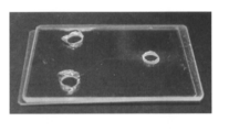
- 1 is an external view showing a nucleic acid extraction device produced in Example 1.
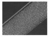
- FIG. 2 is a FESEM photograph of a nucleic acid extraction part of the nucleic acid extraction device produced in Example 1.
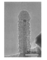
- FIG. FIG. 5B is a partially enlarged view of FIG. 5A. 2 is a TEM photograph of nanowires produced in Example 1.
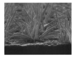
- FIG. 4 is a FESEM photograph of nanowires grown in a nucleic acid extraction part of a nucleic acid extraction device produced in Example 2.
- FIG. 7B is a partially enlarged view of FIG. 7A. It is a figure which shows that the nucleic acid is extended
- nucleic acid extraction device of the present invention the method for producing the device, the nucleic acid extraction method, and the nucleic acid sequence analysis method will be described in detail.
- FIG. 1 is a conceptual diagram showing a nucleic acid extraction method using the nucleic acid extraction device of the present invention (hereinafter sometimes simply referred to as “device”).
- Device a nucleic acid extraction method using the nucleic acid extraction device of the present invention
- Cells or the like injected from one end of the device are pierced by the nanowire in the nucleic acid extraction part where the nanowires are grown in a dense state, whereby the nucleic acid in the cells etc. leaks to the outside and is collected by the external electric field.
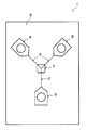
- FIG. 2A shows an example of the device of the present invention.
- a Y-shaped microchannel 3 is formed on a substrate 2.
- a sample input unit 4 At each end of the microchannel 3, a sample input unit 4, a nucleic acid recovery unit 5, and a residue recovery Part 6 is provided. In addition, it is not essential to provide the residue collection unit 6. If the residue collection unit 6 is not provided, the sample input unit 4 may be provided at one end of the linear microchannel 3 and the nucleic acid collection unit 5 may be provided at the other end. Good.
- a nucleic acid extraction unit 7 in which nanowires are grown in a dense state is provided in the center of the microchannel 3.
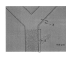
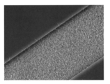
- FIG. 2B is an enlarged photograph of the nucleic acid extraction unit 7 and shows that nanowires 8 are formed in the microchannel 3.
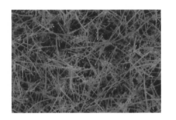
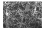
- FIG. 2C is a FESEM photograph of the nucleic acid extraction unit 7.
- the nanowire 8 is formed in a dense state in the nucleic acid extraction unit 7, and cells and the like are perforated by the nanowire 8 when passing through the nucleic acid extraction unit 7.
- the material of the substrate 2 can form a microchannel such as PDMS (poly (dimethylsiloxane)), PMMA (Poly (methyl methacrylate)), PC (polycarbonate), plastic made of hard polyethylene, silicon, glass, etc. There is no particular limitation as long as it can grow.
- the microchannel 3 can be manufactured by using a photolithography technique described later.
- the width and depth of the microchannel 3 are not particularly limited as long as the microchannel 3 is larger than the size of a cell or the like to be extracted and the nanowire 8 can grow sufficiently.
- the sample input unit 4, the nucleic acid recovery unit 5, and the residue recovery unit 6 are provided in particular if the sample can be input directly into the microchannel 3 and the nucleic acid and residue can be recovered directly from the microchannel 3. There is no need.
- the sample input unit 4, the nucleic acid recovery unit 5 and the residue recovery unit 6 are provided, the size, shape, etc. are particularly limited as long as the sample input unit 4, the nucleic acid recovery unit 5 and the microchannel 3 provided on the substrate 2 are connected. There is no restriction
- the catalyst deposition pattern and deposition for growing the nanowires 8 can be produced using electron beam lithography and photolithography techniques.
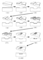
- (1) to (10) in FIG. 3 are an example showing a manufacturing procedure of the device of the present invention.
- a Cr layer is deposited on the substrate 2 by sputtering.
- a positive photoresist is applied by a spin coater, and then a pattern of the microchannel 3 is produced by photolithography. After developing the resist, the Cr layer of the microchannel 3 is etched with a Cr etchant solution.
- the microchannel 3 is produced by a method of selectively etching only the substrate 2. Thereafter, if necessary, through holes for the sample introduction unit 4, the nucleic acid collection unit 5, and the residue collection unit 6 are formed by an ultrasonic drill or the like.
- a Cr layer is deposited again on the substrate 2.
- a positive electron beam resist is applied by a spin coater.
- a pattern of spots for growing nanowires 8 is drawn by electron beam lithography, and after developing the resist, the Cr layer deposited in (4) above is removed at least by the Cr etchant solution.
- the Cr layer on the substrate 2 other than the microchannel 3 deposited in 1) is etched for a time that is not completely removed.
- a nanowire growth catalyst is deposited on the spots formed in (6) above by sputtering, and the resist is removed using a resist removing solution.
- the Cr layer is peeled off with a Cr etchant solution, and a nanowire growth catalyst spot is produced in the microchannel 3. (9)
- the nanowire 8 is grown from the spot produced in the above (8).
- electrodes are formed in the through-hole portions for the sample input part 4, the nucleic acid recovery part 5 and the residue recovery part 6 formed in (3) above, and the micro flow path 3 is covered with a cover glass.
- the device of the present invention is manufactured by covering the formed surface.
- the positive photoresist is not particularly limited as long as it is generally used in the semiconductor manufacturing field, such as TSMR V50, PMER. Further, a negative type photoresist may be used instead of the positive type, and there is no particular limitation as long as it is generally used in the semiconductor manufacturing field, such as SU-8 and KMPR.
- the etchant solution is not particularly limited as long as it can etch Cr, such as H 2 O: Ce (NH 4 ) 2 (NO 3 ) 6 : HClO 4 . Further, the present invention is not limited to Cr, and a material other than Cr may be deposited and used in combination with an etchant that can etch the material.
- the substrate 2 As a method for selectively etching the substrate 2, for example, when quartz glass is used for the substrate, it may be etched with CF 4 gas, SF 6 gas, or the like using a reactive ion etching apparatus. When a material other than quartz glass is used as the substrate 2, the material may be etched by a method that can selectively etch the material.
- the positive electron beam resist is not particularly limited as long as it is generally used in the semiconductor field, such as ZEP520 and PMMA.
- the resist removing solution is not particularly limited as long as it is a common removing solution in the semiconductor field, such as dimethylformamide and acetone.
- the catalyst for growing the nanowire is not particularly limited as long as it is a liquid metal, and examples thereof include gold, platinum, aluminum, copper, iron, cobalt, silver, tin, indium, zinc, and gallium. Further, as will be described later, the nanowire of the present invention has a coating layer formed around the core nanowire grown by the bottom-up method, but the diameter of the core nanowire is almost the same size as the catalyst atom. The catalyst may be appropriately selected in consideration of the diameter of the nanowire.
- the pattern for depositing the catalyst may be arranged so that the spots of the catalyst are in a plover shape or at equal intervals, for example.
- the above procedure is a case where the nanowire growth catalyst is regularly deposited in the microchannel 3 to grow the nanowire 8 radially from the catalyst spot.
- the nanowires 8 are randomly grown in the microchannel 3, after forming the microchannel 3 in the above procedure (3), all Cr is removed, and then a catalyst is deposited on the entire surface of the microchannel 3. Then, a device may be manufactured by the procedures (9) and (10). When a catalyst is deposited on the entire surface of the microchannel 3, the grown nanowires 8 collide with each other, and the nanowires 8 are bent.
- the nanowire 8 of the nucleic acid extraction unit 7 is formed by growing from the catalyst on the microchannel 3 in a bottom-up manner as described above. First, the core nanowire at the center of the nanowire 8 is formed, and then the core nanowire is surrounded. Is provided with a coating layer.
- the method used for forming the core nanowire is not particularly limited as long as it is a general physical vapor deposition method such as pulse laser deposition or VLS (Vapor-Liquid-Solid) method.
- nanowires 8 having substantially the same diameter as one molecule of catalyst grow from the microchannel 3 with the catalyst facing upward.
- the temperature is preferably 400 to 900 ° C. and the pressure is preferably 0.1 to 10 Pa.
- the length of the nanowire 8 is not particularly limited as long as cells or the like are pierced into the nanowire 8 or damaged at the tip to form a hole, but is preferably 2 to 10 ⁇ m. The length of the nanowire 8 may be adjusted appropriately for the deposition time.
- the nanowire of the present invention is formed by forming a coating layer around the core nanowire.
- the method used for forming the coating layer is not particularly limited as long as it is a general vapor deposition method such as sputtering, EB vapor deposition, PVD, or ALD.
- As coating conditions it is necessary to carry out under temperature conditions where the core nanowire does not melt. What is necessary is just to adjust the thickness of a coating layer suitably by changing vapor deposition time.
- the nanowire 8 formed in the nucleic acid extraction unit 7 is inclined with respect to the microchannel 3 rather than in the vertical direction. That is, it is sufficient that a part of the nanowire 8 grows in a direction opposite to the flow of cells or the like, and the nanowire 8 may be formed in a radial manner or bent in an irregular direction.
- the diameter of the nanowire 8 is the size of the target cell, virus, fungus or the like (for example, 1-10 ⁇ m for prokaryotic cells, 5-10 ⁇ m for eukaryotic cells, several tens to several hundred nm for viruses, and 7 for blood cells. The range varies depending on the strength of the cell membrane or the wall, etc., but if the size of the cell punctures the cell when the tip of the nanowire 8 comes into contact with the cell or the like, or the cell or the like is damaged and a hole is formed. There is no particular limitation.
- the diameter of the nanowire 8 may be 10 nm or more, 15 nm or more, 20 nm or more, or 25 nm or more.
- the diameter of the nanowire 8 needs to be at least smaller than that of a cell or the like, and may be, for example, 200 nm or less, 150 nm or less, 100 nm or less, 90 nm or less, 80 nm or less, 70 nm, 60 nm or less, or 50 nm or less.
- Materials for forming the core portion of the nanowire 8 are SiO 2 , Li 2 O, MgO, Al 2 O 3 , CaO, TiO 2 , Mn 2 O 3 , Fe 2 O 3 , CoO, NiO, CuO, ZnO, and Ga 2.
- O 3 , SrO, In 2 O 3 , SnO 2 , Sm 2 O 3 , EuO and the like can be mentioned.
- the coating layer of the nanowire 8 is preferably formed from a material having an isoelectric point lower than that of nucleic acid, and among these materials, SiO 2 and TiO 2 are preferable.
- the catalyst can be arranged in the microchannel 3 at an arbitrary size and interval.
- the shape of the array include a plover shape and an equal interval.
- the diameter of the catalyst spot and the distance between the spots may be arranged so that the nanowires radially grown from the catalyst spot do not interfere with the nanowires grown from the adjacent spot.
- the electrode is not particularly limited as long as it is a commonly used electrode material such as platinum or gold.
- the cultured cells and the like are concentrated by centrifugation or the like as necessary, and injected into the sample input unit 4.
- the cells and the like are attracted to the nucleic acid recovery unit 5.
- the cells etc. come into contact with the nanowire 8 of the nucleic acid extraction section 7 provided in the middle of the micro flow path 3 and pierce, or the nucleic acid in the cells etc. leaks out of the cell from the holes generated by the damage. .
- the nucleic acid Since the nucleic acid is negatively charged, the nucleic acid can be recovered from the cell or the like without being pretreated such as lysis by being attracted to the electrode of the nucleic acid recovery unit 5. Furthermore, since the recovered nucleic acid is elongated in the process of passing between the nanowires 8, it is possible to analyze one molecule using a nanopore sequencer following extraction of the nucleic acid, or to amplify by PCR or the like. In addition, residues such as cells after extraction of nucleic acid, including the case where the residue is caught on the nanowire of the nucleic acid extraction unit 7, are added to the residue collection unit 6, and the nucleic acid collection unit 5 is set to minus, thereby collecting the residue collection unit 6. Can be recovered.
- the applied electric field is not particularly limited as long as it is an electric field in which nucleic acid can migrate, and may be, for example, 1 V or more.
- the nanowire 8 may be formed of a positively charged material such as nickel oxide.
- a biomolecule such as a positively charged protein can be extracted in the same procedure by applying an electric field so that the nucleic acid recovery unit 5 is negative.
- the device of the present invention was produced by the following procedure. First, a Cr layer with a thickness of 250 nm was deposited on quartz glass (Crystal Base Co.) using an RF sputtering apparatus (SVC-700LRF, Sanyu Denshi). Next, a positive type photoresist (TSMR V50, Tokyo Ohka Kogyo Co.) was applied by a spin coater. Thereafter, a microchannel pattern having a width of 25 ⁇ m was produced by photolithography.
- SVC-700LRF RF sputtering apparatus
- a reactive ion etching apparatus RIE-10NR, Samco Co.
- a micro flow channel having a depth of 2 ⁇ m was produced with CF 4 gas.
- a through hole for a sample introduction part, a nucleic acid recovery part, and a residue recovery part having a diameter of 1.5 mm was produced by an ultrasonic drill (SOM-121, Shinoda Co.).
- a Cr layer having a thickness of 10 nm was deposited again on quartz glass, and a positive electron beam resist (ZEP520 A7, Zeon Corp.) was applied by a spin coater.
- a spot pattern for growing nanowires was drawn by electron beam lithography (SPG-724, Sanyu Electron Co.).
- SPG-724 electron beam lithography
- the Cr layer was etched with a Cr etchant solution.
- a gold catalyst having a thickness of 3 nm was deposited inside the microchannel by sputtering, the resist was stripped using dimethylformamide and acetone, and then the Cr layer was stripped with a Cr etchant solution.
- the diameter of the spot (where the nanowire grows) where the gold catalyst was formed was about 300 nm, and the distance from the adjacent spot was about 500 nm.
- a core nanowire was manufactured by performing pulse laser deposition for 10 minutes at room temperature with SnO 2 as a material.
- a coating layer was formed around the core nanowire by sputtering with SiO 2 as a material at room temperature for 15 minutes.
- the device of the present invention was manufactured by covering the surface on which the microchannel was formed with a quartz cover glass having a thickness of 130 ⁇ m.
- FIG. 4 shows the overall appearance of the device fabricated in Example 1.
- FIG. 5A is a FESEM photograph of the nanowire grown in the nucleic acid extraction part
- FIG. 5B is a further enlarged FESEM photograph of FIG. 5A).
- the length of the obtained nanowire was about 2 ⁇ m
- the length of the nucleic acid extraction part was about 500 ⁇ m.
- FIG. 6 is a TEM photograph of one nanowire produced in Example 1.
- the nanowire of the present invention was a nanowire with a diameter of about 30 nm in which SiO 2 was coated around a SnO 2 core nanowire with a diameter of about 10 nm grown by an Au catalyst (about 10 nm).
- Example 2 After the through holes for the sample input part, the nucleic acid recovery part, and the residue recovery part were made with an ultrasonic drill (SOM-121, Shinoda Co.), all the Cr layers were removed with an etchant, and then the microchannel A device was fabricated in the same procedure as in Example 1, except that the gold catalyst was deposited on the entire surface by sputtering to grow nanowires.
- SOM-121 Shinoda Co.
- FIG. 7A is a FESEM photograph of nanowire grown in the nucleic acid extraction part of the device produced in Example 2, and FIG. 7B is a further enlarged FESEM photograph of FIG. 7A. As is clear from the FESEM photographs in FIGS. 7A and 7B, it was confirmed that the nanowires grown from the randomly arranged gold catalyst were bent from the device surface.
- E. coli (ccdB Survival (tm) 2 T1R E. coli, http://products.invitrogen.com/ivgn/product/A10460) was inoculated into 2 ml of LB medium placed in a test tube, and cultured at 37 ° C. for 24 hours with shaking. Went. After completion of the culture, a culture solution containing 100 ⁇ l of E. coli was suspended in 900 ⁇ l of 10 mM Tris buffer and centrifuged at 500 G for 10 minutes.
- nucleic acid-removed solution 1 ⁇ l was taken and mixed with 1 ⁇ l of 10 mM YOYO-1 DMSO solution and left for 30 minutes. Then, 8 ⁇ l of TE buffer was added and diluted to prepare a sample solution stained with nucleic acid.
- FIG. 8 is an image obtained by taking a fluorescent image after nucleic acid extraction into an EB-CCD camera, taking a picture with DVCAM, and editing a movie with Adobe Premiere.
- the bright part at the center of the image is the nucleic acid that has not been extracted from E. coli, and the part surrounded by the white ellipse indicates the nucleic acid that has been extracted from E. coli while extending in the direction of the nucleic acid recovery part.
- FIG. 9 is a FESEM photograph of the nucleic acid extraction part after applying a voltage in the above [Nucleic acid extraction experiment], and it can be seen that the tip of the nanowire is stuck in E. coli. Since the nucleic acid is negatively charged, it is thought that the nucleic acid was extracted from Escherichia coli by attracting the nucleic acid leaked from the pierced portion to the outside of the bacterium to the positively applied electrode. In addition, since a part of the nanowire of the present invention is opposed to the flow direction of the sample, the cells stuck in the nanowire are directly captured by the nanowire and hardly flow in the direction of the nucleic acid recovery unit. Therefore, it is considered that only nucleic acids could be efficiently recovered from cells or the like.
- nanowires having a diameter much smaller than the size of E. coli are formed in a dense state. Therefore, E. coli that has a hole at the tip of the nanowire but did not pierce the nanowire is captured by the densely packed nanowire while flowing through the nucleic acid extraction part, so that only nucleic acid can be efficiently extracted from cells, etc. It is thought that it was able to be recovered.
- nucleic acids are extracted from cells, viruses, fungi, etc. by using a device in which nanowires that are bent or grown radially are formed on a microchannel provided on a substrate of the present invention
- the nucleic acid can be extracted very easily without the need for a pretreatment such as the above.
- the extracted nucleic acid is stretched while passing between a large number of nanowires, it is possible to continue single molecule analysis and the like using a nanopore sequencer, and at medical institutions, universities, companies, research institutions, etc. It is useful for simple and rapid nucleic acid sequence analysis.
Landscapes
- Chemical & Material Sciences (AREA)
- Engineering & Computer Science (AREA)
- Health & Medical Sciences (AREA)
- Biomedical Technology (AREA)
- Life Sciences & Earth Sciences (AREA)
- Genetics & Genomics (AREA)
- Bioinformatics & Cheminformatics (AREA)
- Organic Chemistry (AREA)
- Zoology (AREA)
- Wood Science & Technology (AREA)
- Biotechnology (AREA)
- General Engineering & Computer Science (AREA)
- Crystallography & Structural Chemistry (AREA)
- Plant Pathology (AREA)
- Molecular Biology (AREA)
- Microbiology (AREA)
- Biophysics (AREA)
- Physics & Mathematics (AREA)
- Biochemistry (AREA)
- General Health & Medical Sciences (AREA)
- Analytical Chemistry (AREA)
- Apparatus Associated With Microorganisms And Enzymes (AREA)
- Measuring Or Testing Involving Enzymes Or Micro-Organisms (AREA)
Abstract
細胞等を前処理することなく、細胞等から簡単且つ迅速に核酸を抽出することができるデバイスを提供する。基板上に設けたマイクロ流路上に、マイクロ流路表面から折れ曲がって成長、又は放射状に成長したナノワイヤを設けた核酸抽出用デバイス。
Description
本発明は、核酸抽出用デバイス及び該デバイスの製造方法、並びに核酸抽出方法及び核酸配列解析方法に関する。特に、ナノワイヤを用いて細胞、ウィルス、菌等(以下「細胞等」と記載することもある。)に孔をあけ、電場を印加して前記孔から漏出したDNA及びRNA(以下「核酸」と記載することもある。)を回収することで、細胞等の溶解等の前処理をすることなく、細胞等そのものから迅速且つ簡便に核酸を抽出することができる核酸抽出用デバイス及び該デバイスの製造方法、並びに核酸抽出方法及び核酸配列解析方法に関する。
近年、分子生物学の進歩により、病院等の医療機関の現場では、遺伝子欠失や薬剤感受性SNP(Single Nucleotide Polymorphism)などの遺伝子診断、病原菌等による感染症の診断やアレルゲンの診断等、遺伝子解析に基づく診断等が広がりつつあり、細胞等から遺伝子である核酸を効率的且つ簡便な操作で抽出する方法が求められている。
核酸を含有する細胞等から核酸を分離、抽出する方法としては、例えば、フェノール・クロロホルム抽出法、核酸含有溶液をエタノール溶液で沈殿して核酸を分離する方法、酵素を用いて細胞等を溶解して核酸を分離する方法、磁気ビーズを用いた核酸抽出方法、フィルターを用いた核酸抽出方法等、様々な方法が知られている。
しかしながら、フェノール・クロロホルム抽出法では、フェノール・クロロホルムを用いてタンパク質や脂質など細胞等の水に難溶性の成分を変性させることで除去しているが、核酸の抽出には遠心分離工程を繰り返す等、操作に時間がかかるとともに手技を習得する必要がある上、核酸の抽出には危険な試薬を必要とする問題がある。また、エタノール溶液で沈降する方法も、酵素を用いる方法も、何れも核酸を抽出するには操作に時間がかかるという問題がある。更に、磁気ビーズを用いた方法においても、磁気ビーズが精製物に混入するといった問題や、核酸が吸着するビーズの表面積が小さく核酸収量が低い等の問題がある。
一方、抽出された核酸の解析は、酵素法、化学分解法等が知られており、現在はこれらの原理を使用した自動シークエンスキット等も販売されている。
ところで、DNA塩基配列の超高速解析、ウィルスの超微量かつ超高速検出、花粉などのアレルゲンの超高感度かつ超高速検出などは、安心、安全、健康な社会実現のためには必要不可欠な技術である。しかしながら、従来の技術では解析すべきDNAのPCR等を用いた増幅工程が必要であり、迅速にDNA解析をすることができなかった。その問題点を解決するため、ナノポアシーケンサにより1本のDNAから塩基識別できる1分子解析技術(非特許文献1「M. Tsutsui et al.,“Identifying single nucleotides by tunnelling current”, Nat. Nanotech., 2010,5,286-290.」参照)が知られている。また、前記1分子解析のサンプルとして使用するために、長鎖DNAを一本のDNAに伸長させるDNA伸長技術も知られている(非特許文献2「安井等、「ナノ構造体を用いたDNA解析」、NEW GLASS、2009、Vol.24、No.1、p22-27」参照)。
前記伸長技術は、石英ガラス上のナノ流路に電子線リソグラフィとフォトリソグラフィとを組み合わせて、ナノピラーと呼ばれる直径が約500nm、高さが約4000nmのSiO2からなる竹林のような形状のものを微細加工技術(トップダウン方式)で形成する。そして、細胞等から抽出した長鎖DNAをナノピラーの間を通過させることで、上記1分子解析に使用することが可能となる伸長したDNAを得る技術である。
しかしながら、上記伸長技術に用いられるDNAは、従来のフェノール・クロロホルム抽出法等の従来法により抽出されたDNAであり、細胞等から超高感度かつ超高速でDNA配列を解析するためには、依然として時間がかかるという問題がある。
なお、基板上に設けたナノワイヤに細胞等を擦り付けるように移動させることで、薬品や酵素等を使用しなくても、細胞等を破砕できることは知られている(非特許文献3「Jung Kim et al., “Nanowire-integrated microfluidic devices for facile and reagent-free mechanical cell lysis”, Lab on Chip,2012, 12, 2914-2921」参照)。しかしながら、非特許文献3に記載されている技術では、単に細胞等を破砕するにとどまり、細胞等から選択的に核酸を抽出することは確認されていない。
本発明は、上記従来の問題を解決するためになされた発明であり、鋭意研究を行ったところ、非特許文献3に記載されているナノワイヤは基板からほぼ鉛直方向に配列したものであり細胞等の流れ方向に向いていないことを見出した。そして、基板上に設けたマイクロ流路内に、触媒を用いてボトムアップで直径の細いナノワイヤをランダム又は放射状に成長させた核酸抽出部を形成し、細胞等がナノワイヤに突き刺さる、又は、ナノワイヤの先端で細胞等が損傷を受けることで形成された孔から核酸が漏出し、該漏出した核酸が外部電場を印加することで電極に引き寄せられ回収されることで、細胞等の溶解等の前処理工程を経ずに、細胞等自体から直接核酸を抽出できることを新たに見出し、本発明を完成した。
すなわち、本発明の目的は、細胞等から核酸を抽出するための核酸抽出用デバイス及び該デバイスの製造方法、並びに核酸抽出方法及び核酸配列解析方法を提供することである。
本発明は、以下に示す、核酸抽出用デバイス及び該デバイスの製造方法、並びに核酸抽出方法及び核酸配列解析方法に関する。
(1)基板上に設けたマイクロ流路上に、マイクロ流路表面から折れ曲がって成長、又は放射状に成長したナノワイヤを設けた核酸抽出用デバイス。
(2)前記ナノワイヤが、触媒を用いてボトムアップで成長したコアナノワイヤの表面に、被覆層が形成されたナノワイヤである上記(1)に記載の核酸抽出用デバイス。
(3)前記ナノワイヤが、細胞、ウィルス、または菌から選ばれるサンプルに孔をあける上記(1)又は(2)に記載の核酸抽出用デバイス。
(4)前記マイクロ流路の一端にサンプル投入部、他端に核酸回収部が形成され、前記サンプル投入部及び前記核酸回収部の間に前記ナノワイヤが成長した核酸抽出部が形成されている上記(1)~(3)の何れか一項に記載の核酸抽出用デバイス。
(5)前記サンプル投入部と前記核酸抽出部の間のマイクロ流路に、他端に残渣回収部を有するマイクロ流路の一端が接続している上記(4)に記載の核酸抽出用デバイス。
(6)前記サンプル投入部、前記核酸回収部、及び前記残渣回収部に電極が形成されている上記(4)または(5)に記載の核酸抽出用デバイス。
(7)基板上にマイクロ流路を形成する工程、前記マイクロ流路にチドリ状又は等間隔、又は前記マイクロ流路全体に触媒を堆積する工程、前記触媒からコアナノワイヤを放射状又は折れ曲がって成長させる工程、及び前記コアナノワイヤに被覆層を設ける工程、を含む核酸抽出用デバイスの製造方法。
(8)基板上に、サンプル投入部、核酸回収部、及び残渣回収部を形成する工程を更に含む上記(7)に記載の核酸抽出用デバイスの製造方法。
(9)前記サンプル投入部、前記核酸回収部、及び前記残渣回収部に電極を形成する工程を更に含む上記(8)に記載の核酸抽出用デバイスの製造方法。
(10)細胞、ウィルス、または菌から選ばれるサンプルからの核酸抽出方法であって、基板上に形成されたマイクロ流路表面から折れ曲がって成長、又は放射状に成長したナノワイヤを含む核酸抽出用デバイスのマイクロ流路の一端にサンプルを注入する工程、前記マイクロ流路のサンプル注入側をマイナス、前記ナノワイヤを挟んでサンプル注入側と反対側をプラスになるように電場を印加する工程、マイクロ流路をプラスに印加した側から伸長した核酸を回収する工程、を含む核酸抽出方法。
(11)細胞、ウィルス、または菌から選ばれるサンプルからの核酸配列解析方法であって、基板上に形成されたマイクロ流路表面から折れ曲がって成長、又は放射状に成長したナノワイヤを含む核酸抽出用デバイスのマイクロ流路の一端にサンプルを注入する工程、前記マイクロ流路のサンプル注入側をマイナス、前記ナノワイヤを挟んでサンプル注入側と反対側をプラスになるように電場を印加する工程、マイクロ流路をプラスに印加した側から伸長した核酸を回収する工程、前記伸長した核酸からナノポアシーケンサを用いて核酸配列を解析する工程、を含む核酸配列解析方法。
(2)前記ナノワイヤが、触媒を用いてボトムアップで成長したコアナノワイヤの表面に、被覆層が形成されたナノワイヤである上記(1)に記載の核酸抽出用デバイス。
(3)前記ナノワイヤが、細胞、ウィルス、または菌から選ばれるサンプルに孔をあける上記(1)又は(2)に記載の核酸抽出用デバイス。
(4)前記マイクロ流路の一端にサンプル投入部、他端に核酸回収部が形成され、前記サンプル投入部及び前記核酸回収部の間に前記ナノワイヤが成長した核酸抽出部が形成されている上記(1)~(3)の何れか一項に記載の核酸抽出用デバイス。
(5)前記サンプル投入部と前記核酸抽出部の間のマイクロ流路に、他端に残渣回収部を有するマイクロ流路の一端が接続している上記(4)に記載の核酸抽出用デバイス。
(6)前記サンプル投入部、前記核酸回収部、及び前記残渣回収部に電極が形成されている上記(4)または(5)に記載の核酸抽出用デバイス。
(7)基板上にマイクロ流路を形成する工程、前記マイクロ流路にチドリ状又は等間隔、又は前記マイクロ流路全体に触媒を堆積する工程、前記触媒からコアナノワイヤを放射状又は折れ曲がって成長させる工程、及び前記コアナノワイヤに被覆層を設ける工程、を含む核酸抽出用デバイスの製造方法。
(8)基板上に、サンプル投入部、核酸回収部、及び残渣回収部を形成する工程を更に含む上記(7)に記載の核酸抽出用デバイスの製造方法。
(9)前記サンプル投入部、前記核酸回収部、及び前記残渣回収部に電極を形成する工程を更に含む上記(8)に記載の核酸抽出用デバイスの製造方法。
(10)細胞、ウィルス、または菌から選ばれるサンプルからの核酸抽出方法であって、基板上に形成されたマイクロ流路表面から折れ曲がって成長、又は放射状に成長したナノワイヤを含む核酸抽出用デバイスのマイクロ流路の一端にサンプルを注入する工程、前記マイクロ流路のサンプル注入側をマイナス、前記ナノワイヤを挟んでサンプル注入側と反対側をプラスになるように電場を印加する工程、マイクロ流路をプラスに印加した側から伸長した核酸を回収する工程、を含む核酸抽出方法。
(11)細胞、ウィルス、または菌から選ばれるサンプルからの核酸配列解析方法であって、基板上に形成されたマイクロ流路表面から折れ曲がって成長、又は放射状に成長したナノワイヤを含む核酸抽出用デバイスのマイクロ流路の一端にサンプルを注入する工程、前記マイクロ流路のサンプル注入側をマイナス、前記ナノワイヤを挟んでサンプル注入側と反対側をプラスになるように電場を印加する工程、マイクロ流路をプラスに印加した側から伸長した核酸を回収する工程、前記伸長した核酸からナノポアシーケンサを用いて核酸配列を解析する工程、を含む核酸配列解析方法。
本発明の核酸抽出用デバイスは、基板上のマイクロ流路に形成されたナノワイヤに細胞等が突き刺さる、又は、ナノワイヤの先端で細胞等が損傷を受ける等の理由により、細胞等の膜又は壁に孔が生じ、漏出した核酸を外部電場により引き寄せることでマイクロ流路から抽出することができるので、従来必要であった細胞等の溶解等の前処理が不要であることから有機廃液等の問題がなく、また、簡単且つ迅速に超微量の細胞等から直接核酸を抽出することができる。
本発明のナノワイヤは、触媒を用いてボトムアップでコアとなるナノワイヤが形成され、次いで、該ナノワイヤの周囲に被覆層が形成されることから、ナノワイヤの直径を所望の太さにコントロールすることができ、核酸を抽出するサンプルの大きさに応じて、ナノワイヤの太さを変えることができる。また、ナノワイヤのコア部分と被覆部分が別々に形成されることから、被覆部分のみを核酸等と静電的相互作用しない材料から形成することができる。
更に、電子線リソグラフィ及びフォトリソグラフィの技術を駆使することで、基板上のマイクロ流路に所定の間隔で堆積した触媒から放射状に成長したナノワイヤ、又は、マイクロ流路全体に触媒を塗布することで折れ曲がって成長した密集状態のナノワイヤを得ることができる。したがって、何れの場合も得られたナノワイヤの一部は細胞等の流れ方向に必ず対向するので、確実に細胞等に孔をあけることができる。
また、細胞等から抽出された核酸は、ナノワイヤの間を通過する間に伸長されることから核酸の抽出と伸長とを同時に行うことができる。したがって、核酸の抽出に引き続きナノポアシーケンサを用いて1分子解析をすることで、細胞等の核酸配列を簡便且つ迅速に決定することができる。
以下に、本発明の核酸抽出用デバイス及び該デバイスの製造方法、並びに核酸抽出方法及び核酸配列解析方法について詳しく説明する。
図1は、本発明の核酸抽出用デバイス(以下、単に「デバイス」と記載することもある。)を用いた核酸の抽出方法を示す概念図である。デバイスの一端から注入された細胞等は、ナノワイヤが密集状態で成長した核酸抽出部において、ナノワイヤにより孔をあけられることで細胞等内の核酸が外部に漏出し、外部電場により回収される。
図2Aは、本発明のデバイスの一例を示している。本発明のデバイス1は、基板2上にY字状のマイクロ流路3が形成されており、マイクロ流路3のそれぞれの端部には、サンプル投入部4、核酸回収部5、及び残渣回収部6が設けられている。なお、残渣回収部6を設けることは必須ではなく、残渣回収部6を設けない場合は、直線状のマイクロ流路3の一端にサンプル投入部4、他端に核酸回収部5を設ければよい。マイクロ流路3の中央には、ナノワイヤが密集状態で成長した核酸抽出部7が設けられている。本発明のデバイス1を用いて核酸を抽出する時は、サンプル投入部4、核酸回収部5、及び残渣回収部6へ電場を印加する図示しない電源が用いられる。なお、サンプル投入部4、核酸回収部5、及び残渣回収部6への電場の印加は、デバイス1の製造時にサンプル投入部4、核酸回収部5、及び残渣回収部6に形成した図示しない電極を用いてもよいし、サンプル投入部4、核酸回収部5、残渣回収部6の穴に外部から電極を差し込んでもよい。図2Bは、核酸抽出部7の拡大写真で、マイクロ流路3内にナノワイヤ8が形成されていることを示す。図2Cは、核酸抽出部7のFESEM写真である。図2Cから明らかなように、核酸抽出部7ではナノワイヤ8が密集状態で形成されており、細胞等は核酸抽出部7を通過する際にナノワイヤ8により孔があけられる。
基板2の材料は、PDMS(poly(dimethylsiloxane))、PMMA(Poly(methyl methacrylate))、PC(polycarbonate)、硬質ポリエチレン製等のプラスチック、シリコン、ガラス等、マイクロ流路が形成でき、ナノワイヤ8が成長できるものであれば特に制限はない。
マイクロ流路3は後述するフォトリソグラフィ技術を用いて作製することができる。マイクロ流路3の幅及び深さは、抽出したい細胞等の大きさ以上であって、ナノワイヤ8が十分成長できるサイズであれば特に制限はない。
サンプル投入部4、核酸回収部5、及び残渣回収部6は、マイクロ流路3に直接サンプルを投入することができ、また、核酸や残渣をマイクロ流路3から直接回収することができれば特に設ける必要はない。サンプル投入部4、核酸回収部5、及び残渣回収部6を設ける場合には、核酸や基板2上に設けたマイクロ流路3と接続するように設けられていれば、サイズ、形状等は特に制限はなく、超音波ドリル、サンドブラスター等で形成されればよい。
マイクロ流路3及び核酸抽出部7において、ナノワイヤ8を成長させるための触媒の堆積パターン及び堆積は、電子線リソグラフィ及びフォトリソグラフィ技術を用いて作製することができる。図3の(1)~(10)は、本発明のデバイスの作製手順を示した一例である。
(1)基板2上にCr層をスパッタで堆積する。
(2)ポジ型フォトレジストをスピンコータで塗布し、次いで、フォトリソグラフィによりマイクロ流路3のパターンを作製する。レジストを現像した後、Crエッチャント液にてマイクロ流路3のCr層をエッチングする。
(3)基板2のみを選択的にエッチングする手法により、マイクロ流路3を作製する。その後、必要に応じてサンプル投入部4、核酸回収部5、及び残渣回収部6用の貫通穴を超音波ドリル等により形成する。
(4)Cr層を再度基板2上に堆積させる。
(5)ポジ型電子線レジストをスピンコータにより塗布する。
(6)電子線リソグラフィにより、ナノワイヤ8を成長させるスポットのパターンを描画し、レジストの現像後、Crエッチャント液により、上記(4)で堆積した厚さのCr層は少なくとも除去されるが、(1)で堆積したマイクロ流路3以外の基板2上のCr層は完全に除去されない時間エッチングされる。
(7)ナノワイヤ成長用の触媒を、上記(6)で形成したスポットにスパッタリングにより堆積させ、レジスト除去液を用いてレジストを剥離する。
(8)Cr層をCrエッチャント液により剥離して、マイクロ流路3内にナノワイヤ成長用触媒のスポットを作製する。
(9)上記(8)で作製したスポットから、ナノワイヤ8を成長させる。
(10)必要に応じて、上記(3)で形成されたサンプル投入部4、核酸回収部5、及び残渣回収部6用の貫通穴部分に電極を形成し、カバーガラスでマイクロ流路3を形成した面に蓋をすることで、本発明のデバイスを作製する。
(2)ポジ型フォトレジストをスピンコータで塗布し、次いで、フォトリソグラフィによりマイクロ流路3のパターンを作製する。レジストを現像した後、Crエッチャント液にてマイクロ流路3のCr層をエッチングする。
(3)基板2のみを選択的にエッチングする手法により、マイクロ流路3を作製する。その後、必要に応じてサンプル投入部4、核酸回収部5、及び残渣回収部6用の貫通穴を超音波ドリル等により形成する。
(4)Cr層を再度基板2上に堆積させる。
(5)ポジ型電子線レジストをスピンコータにより塗布する。
(6)電子線リソグラフィにより、ナノワイヤ8を成長させるスポットのパターンを描画し、レジストの現像後、Crエッチャント液により、上記(4)で堆積した厚さのCr層は少なくとも除去されるが、(1)で堆積したマイクロ流路3以外の基板2上のCr層は完全に除去されない時間エッチングされる。
(7)ナノワイヤ成長用の触媒を、上記(6)で形成したスポットにスパッタリングにより堆積させ、レジスト除去液を用いてレジストを剥離する。
(8)Cr層をCrエッチャント液により剥離して、マイクロ流路3内にナノワイヤ成長用触媒のスポットを作製する。
(9)上記(8)で作製したスポットから、ナノワイヤ8を成長させる。
(10)必要に応じて、上記(3)で形成されたサンプル投入部4、核酸回収部5、及び残渣回収部6用の貫通穴部分に電極を形成し、カバーガラスでマイクロ流路3を形成した面に蓋をすることで、本発明のデバイスを作製する。
上記手順において、ポジ型フォトレジストとしてはTSMR V50、PMER等、半導体製造分野で一般的に使用されているものであれば特に制限はない。また、ポジ型に代え、ネガティブ型のフォトレジストを用いてもよく、SU-8、KMPR等、半導体製造分野で一般的に使用されているものであれば特に制限はない。
エッチャント液は、H2O:Ce(NH4)2(NO3)6:HClO4等、Crをエッチングできるものであれば特に制限はない。また、本発明はCrに限定されるのではなく、Cr以外の材料を堆積し、該材料をエッチングできるエッチャント液と組み合わせて用いてもよい。
基板2を選択的にエッチングする手法としては、例えば、基板に石英ガラスを用いた場合は、反応性イオンエッチング装置を用いて、CF4ガス、SF6ガス等でエッチングすればよい。基板2として石英ガラス以外の材料を用いた場合は、当該材料を選択的にエッチングできる方法でエッチングすればよい。
ポジ型電子線レジストとしては、ZEP520、PMMA等、半導体分野で一般的に用いられているものであれば特に制限はない。また、レジストの除去液としては、ジメチルホルムアミドとアセトン等、半導体分野で一般的な除去液であれば特に制限はない。
ナノワイヤを成長させるための触媒としては、液体になる金属であれば特に制限はなく、金、プラチナ、アルミ、銅、鉄、コバルト、銀、錫、インジウム、亜鉛、ガリウム等が挙げられる。また、後述するように、本発明のナノワイヤはボトムアップ方式で成長したコアナノワイヤの周囲に被覆層が形成されるが、コアナノワイヤの直径は触媒原子とほぼ同じ大きさになることから、所望のナノワイヤの直径を考慮し、触媒を適宜選択すればよい。
また、触媒を堆積するパターンは、例えば、触媒のスポットがチドリ状又は等間隔になるように配列すればよい。
なお、上記の手順は、マイクロ流路3内に、ナノワイヤ成長用の触媒を規則正しく堆積してナノワイヤ8を触媒のスポットから放射状に成長させる場合である。マイクロ流路3内にナノワイヤ8をランダムに成長させる場合は、上記手順(3)でマイクロ流路3を形成した後、全てのCrを除去し、次いでマイクロ流路3の全面に触媒を堆積し、次いで上記(9)及び(10)の手順によりデバイスを作製すればよい。マイクロ流路3の全面に触媒を堆積した場合は、成長したナノワイヤ8同士がぶつかり合い、ナノワイヤ8は折れ曲がって形成される。
核酸抽出部7のナノワイヤ8は、上記のとおりマイクロ流路3上の触媒からボトムアップ方式で成長させることで形成され、先ずナノワイヤ8の中心部分のコアナノワイヤが形成され、次いで、コアナノワイヤの周りに被覆層が設けられる。コアナノワイヤの形成に用いる手法は、パルスレーザーデポジション、VLS(Vapor-Liquid-Solid)法等、一般的な物理蒸着法であれば特に制限はない。
コアナノワイヤは、触媒1分子とほぼ同じ直径のナノワイヤ8がマイクロ流路3から触媒を上にして成長する。直径をコントロールするには、所望の大きさとなる触媒分子を選択するとともに、触媒が無くならない温度及び圧力でコアナノワイヤを成長させる必要がある。触媒により異なるものの、温度は400~900℃、圧力は0.1~10Paにすることが好ましい。また、ナノワイヤ8の長さは、細胞等がナノワイヤ8に突き刺さる、又は先端で損傷を受け孔が生じれば特に制限はないが、2~10μmが好ましい。ナノワイヤ8の長さは、蒸着時間を適宜調整すればよい。
コアナノワイヤが成長した後、コアナノワイヤの周りに被覆層を形成することで本発明のナノワイヤが形成される。被覆層の形成に用いる手法は、スパッタリング、EB蒸着、PVD、ALD等の一般的な蒸着法であれば特に制限はない。被覆条件としては、コアナノワイヤが溶けない温度条件で行う必要があり、コアナノワイヤの材料によるものの、800℃以下で行うことが望ましい。被覆層の厚さは、蒸着時間を変えることで適宜調整すればよい。
本発明では、細胞等がマイクロ流路3内を移動する際にナノワイヤ8に突き刺さる、又は、ナノワイヤ8の先端で細胞等が損傷を受ける等の理由により、細胞等の膜又は壁に孔が生じ、その孔から細胞等内の核酸が外部に漏出すると考えられる。そのため、核酸抽出部7に形成されるナノワイヤ8は、マイクロ流路3に対して鉛直方向ではなく傾斜している。つまり、細胞等の流れに対向する方向にナノワイヤ8の一部が成長していればよく、放射状に形成されていても、不規則な方向に折れ曲がって形成されていてもよい。また、ナノワイヤ8の直径は、目的とする細胞、ウィルス、菌等の大きさ(例えば、原核細胞は1~10μm、真核細胞は5~10μm、ウィルスは数10~数100nm、血球細胞は7~15μm等)及び細胞膜又は壁の強度等により範囲は異なるが、細胞等にナノワイヤ8の先端が当接した時に細胞等を突き刺す、又は、細胞等が損傷して孔が生じる大きさであれば特に制限はない。例えば、ナノワイヤ8の直径は、10nm以上、15nm以上、20nm以上、又は25nm以上であればよい。また、ナノワイヤ8の直径は、少なくとも細胞等よりは小さい必要があり、例えば、200nm以下、150nm以下、100nm以下、90nm以下、80nm以下、70nm、60nm以下、又は50nm以下であればよい。
ナノワイヤ8のコア部分を形成する材料は、SiO2、Li2O、MgO、Al2O3、CaO、TiO2、Mn2O3、Fe2O3、CoO、NiO、CuO、ZnO、Ga2O3、SrO、In2O3、SnO2、Sm2O3、EuO等が挙げられる。また、ナノワイヤ8の表面は、細胞等の孔から漏出した核酸が静電的相互作用によりナノワイヤに吸着しない方が好ましい。従って、ナノワイヤ8の被覆層は、核酸の等電点より低い等電点の材料から形成されることが好ましく、それら材料の中でも、SiO2、TiO2が好ましい。
上記のとおり、電子線リソグラフィ及びフォトリソグラフィの技術を駆使することで、マイクロ流路3内に、触媒を任意の大きさ及び間隔で配列することができる。配列の形状としては、チドリ状、等間隔等が挙げられる。触媒スポットの直径、及びスポットとスポットとの間隔は、触媒スポットから放射状に成長したナノワイヤが、隣のスポットから成長したナノワイヤと干渉しない程度の大きさ及び間隔に配列すればよい。
電極としては、白金、金等、一般的に用いられている電極の材料であれば特に制限はない。
次に、本発明のデバイスを用いた核酸の抽出方法について図2A~図2Cを用いて説明する。培養した細胞等は、必要に応じて遠心分離等で濃縮され、サンプル投入部4に注入される。次いで、細胞等から核酸を抽出する場合、サンプル投入部4がマイナス、核酸回収部5がプラスとなるように電圧を印加すると、細胞等は核酸回収部5に引き寄せられる。そして、マイクロ流路3の途中に設けられている核酸抽出部7のナノワイヤ8に細胞等が当接して突き刺り、又は損傷して生じた孔から細胞等内の核酸が細胞外に漏出する。そして、核酸はマイナスに帯電していることから、核酸回収部5の電極に引き寄せられることで、溶解等の前処理をしなくても、細胞等から核酸を回収することができる。更に、回収された核酸は、ナノワイヤ8の間を通る過程で伸長されることから、核酸の抽出に引き続きナノポアシーケンサを用いて1分子解析することもできるし、PCR等で増幅することもできる。また、核酸を抽出した後の細胞等の残渣は、核酸抽出部7のナノワイヤに引っかかっている場合も含め、残渣回収部6をプラス、核酸回収部5をマイナスにすることで、残渣回収部6で回収することができる。印加する電場は、核酸が泳動可能な電場であれば特に制限はなく、例えば、1V以上であればよい。
なお、上記の例は、細胞等からマイナスに帯電する核酸を抽出する場合であるが、例えば、酸化ニッケル等の正に帯電する材料でナノワイヤ8の被覆層を形成してもよい。この場合、核酸回収部5がマイナスとなるように電場をかけることで、正に帯電するタンパク質等の生体分子を同様の手順で抽出することも可能である。
以下に実施例を掲げ、本発明を具体的に説明するが、この実施例は単に本発明の説明のため、その具体的な態様の参考のために提供されているものである。これらの例示は本発明の特定の具体的な態様を説明するためのものであるが、本願で開示する発明の範囲を限定したり、あるいは制限することを表すものではない。
<実施例1>
〔デバイスの作製〕
本発明のデバイスは以下の手順により作製した。先ず、RFスパッタ装置(SVC-700LRF、Sanyu Denshi)を用いて石英ガラス上(Crystal Base Co.)に250nmの厚さのCr層を堆積させた。次に、ポジ型フォトレジスト(TSMR V50、Tokyo Ohka Kogyo Co.)をスピンコータにより塗布した。その後、フォトリソグラフィにより幅25μmのマイクロ流路パターンを作製した。レジストを現像した後、Crエッチャント液(H2O:Ce(NH4)2(NO3)6:HClO4=85:10:5(質量%比))にてCr層を5分間エッチングした。反応性イオンエッチング装置(RIE-10NR、Samco Co.)を用いてCF4ガスにより、深さ2μmのマイクロ流路を作製した。直径1.5mmのサンプル投入部、核酸回収部、及び残渣回収部用の貫通孔を超音波ドリル(SOM-121、Shinoda Co.)により作製した。次に、厚さ10nmのCr層を再度石英ガラス上に堆積させ、ポジ型電子線レジスト(ZEP520 A7、Zeon Corp.)をスピンコータにより塗布した。次に、電子線リソグラフィ(SPG-724、Sanyu Electron Co.)により、ナノワイヤを成長させるスポットのパターンを描画した。レジストの現像後、Crエッチャント液により、Cr層をエッチングした。厚さ3nmの金触媒を、スパッタリングによりマイクロ流路内部に堆積させ、ジメチルホルムアミド及びアセトンを用いて、レジストを剥離した後、Cr層をCrエッチャント液により剥離した。この時の金触媒が形成されているスポット(ナノワイヤが成長する箇所)の直径は約300nm、隣のスポットとの距離は約500nmであった。次いで、SnO2を材料に、室温で10Pa、20分間パルスレーザーデポジションを行うことでコアナノワイヤを作製した。次いで、SiO2を材料に、室温で15分間スパッタリングを行うことでコアナノワイヤの周りに被覆層を形成した。最後に、厚さ130μmの石英製カバーガラスでマイクロ流路を形成した面に蓋をすることで、本発明のデバイスを作製した。
〔デバイスの作製〕
本発明のデバイスは以下の手順により作製した。先ず、RFスパッタ装置(SVC-700LRF、Sanyu Denshi)を用いて石英ガラス上(Crystal Base Co.)に250nmの厚さのCr層を堆積させた。次に、ポジ型フォトレジスト(TSMR V50、Tokyo Ohka Kogyo Co.)をスピンコータにより塗布した。その後、フォトリソグラフィにより幅25μmのマイクロ流路パターンを作製した。レジストを現像した後、Crエッチャント液(H2O:Ce(NH4)2(NO3)6:HClO4=85:10:5(質量%比))にてCr層を5分間エッチングした。反応性イオンエッチング装置(RIE-10NR、Samco Co.)を用いてCF4ガスにより、深さ2μmのマイクロ流路を作製した。直径1.5mmのサンプル投入部、核酸回収部、及び残渣回収部用の貫通孔を超音波ドリル(SOM-121、Shinoda Co.)により作製した。次に、厚さ10nmのCr層を再度石英ガラス上に堆積させ、ポジ型電子線レジスト(ZEP520 A7、Zeon Corp.)をスピンコータにより塗布した。次に、電子線リソグラフィ(SPG-724、Sanyu Electron Co.)により、ナノワイヤを成長させるスポットのパターンを描画した。レジストの現像後、Crエッチャント液により、Cr層をエッチングした。厚さ3nmの金触媒を、スパッタリングによりマイクロ流路内部に堆積させ、ジメチルホルムアミド及びアセトンを用いて、レジストを剥離した後、Cr層をCrエッチャント液により剥離した。この時の金触媒が形成されているスポット(ナノワイヤが成長する箇所)の直径は約300nm、隣のスポットとの距離は約500nmであった。次いで、SnO2を材料に、室温で10Pa、20分間パルスレーザーデポジションを行うことでコアナノワイヤを作製した。次いで、SiO2を材料に、室温で15分間スパッタリングを行うことでコアナノワイヤの周りに被覆層を形成した。最後に、厚さ130μmの石英製カバーガラスでマイクロ流路を形成した面に蓋をすることで、本発明のデバイスを作製した。
図4は実施例1で作製したデバイスの全体の外観を示している。図5Aは核酸抽出部で成長したナノワイヤのFESEM写真、図5Bは図5A)を更に拡大したFESEM写真である。得られたナノワイヤの長さは約2μm、核酸抽出部の長さは約500μmであった。
また、図6は、実施例1で作製したナノワイヤの一本のTEM写真である。図6から明らかなように、本発明のナノワイヤは、Au触媒(約10nm)により成長した直径約10nmのSnO2コアナノワイヤの周りにSiO2が被覆した直径約30nmのナノワイヤであった。
<実施例2>
サンプル投入部、核酸回収部、及び残渣回収部用の貫通穴を超音波ドリル(SOM-121、Shinoda Co.)により作製後、全てのCr層をエッチャントで除去し、次いで、マイクロ流路内の全体に金触媒をスパッタリングにより堆積してナノワイヤを成長させた以外は、実施例1と同様の手順でデバイスを作製した。
サンプル投入部、核酸回収部、及び残渣回収部用の貫通穴を超音波ドリル(SOM-121、Shinoda Co.)により作製後、全てのCr層をエッチャントで除去し、次いで、マイクロ流路内の全体に金触媒をスパッタリングにより堆積してナノワイヤを成長させた以外は、実施例1と同様の手順でデバイスを作製した。
図7Aは実施例2で作製したデバイスの核酸抽出部で成長したナノワイヤのFESEM写真で、図7Bは図7Aを更に拡大したFESEM写真である。図7A及び図7BのFESEM写真から明らかなように、ランダムに配置した金触媒から成長したナノワイヤは、デバイス表面から折れ曲がって成長することが確認された。
<実施例3>
〔サンプルの調整〕
試験管に入れた2mlのLB培地に大腸菌(ccdB Survival(tm)2 T1R大腸菌、http://products.invitrogen.com/ivgn/product/A10460)を接種し、37℃で24時間、振とう培養を行った。培養終了後、100μlの大腸菌を含む培養液を、10mMのTrisバッファー900μlに懸濁し、500Gで10分間遠心分離を行った。遠心分離後、上清950μlを除去し、沈殿物を10mMのTrisバッファー950μlに再懸濁し、前記と同様の遠心条件で遠心分離を行った。再懸濁及び遠心分離を前記と同様の条件で更に1回行った後、上清を除いた沈殿物を10mMのTrisバッファー900μlに再懸濁した。大腸菌を含む再懸濁液90μlにDNase I溶液(濃度は5000U/μl)10μlを添加し、37℃で1時間インキュベートを行い、大腸菌の周囲の核酸を除去した。核酸を除去した溶液を1μlとり、10mM YOYO-1 DMSO溶液1μlと混合して30分置いたのち8μlのTEバッファーを加えて希釈することで核酸を染色したサンプル溶液を作製した。
〔サンプルの調整〕
試験管に入れた2mlのLB培地に大腸菌(ccdB Survival(tm)2 T1R大腸菌、http://products.invitrogen.com/ivgn/product/A10460)を接種し、37℃で24時間、振とう培養を行った。培養終了後、100μlの大腸菌を含む培養液を、10mMのTrisバッファー900μlに懸濁し、500Gで10分間遠心分離を行った。遠心分離後、上清950μlを除去し、沈殿物を10mMのTrisバッファー950μlに再懸濁し、前記と同様の遠心条件で遠心分離を行った。再懸濁及び遠心分離を前記と同様の条件で更に1回行った後、上清を除いた沈殿物を10mMのTrisバッファー900μlに再懸濁した。大腸菌を含む再懸濁液90μlにDNase I溶液(濃度は5000U/μl)10μlを添加し、37℃で1時間インキュベートを行い、大腸菌の周囲の核酸を除去した。核酸を除去した溶液を1μlとり、10mM YOYO-1 DMSO溶液1μlと混合して30分置いたのち8μlのTEバッファーを加えて希釈することで核酸を染色したサンプル溶液を作製した。
〔核酸の抽出実験〕
上記サンプル溶液2μlを実施例2で作製したデバイスのサンプル投入部に注入し、サンプル投入部及び核酸回収部に白金電極を挿入して、サンプル投入部がマイナス、核酸回収部がプラスとなるように、200Vの電圧を90分間印加した。
上記サンプル溶液2μlを実施例2で作製したデバイスのサンプル投入部に注入し、サンプル投入部及び核酸回収部に白金電極を挿入して、サンプル投入部がマイナス、核酸回収部がプラスとなるように、200Vの電圧を90分間印加した。
図8は、核酸抽出後の蛍光画像をEB-CCDカメラに取り込み、DVCAMにて撮影し、Adobe premiereにて動画編集した画像である。画像中央の明るい部分は大腸菌から未抽出の状態の核酸で、白色の楕円で囲った部分は大腸菌から核酸回収部方向に伸長しながら抽出された核酸を示している。
図9は、上記〔核酸の抽出実験〕で電圧を印加した後の核酸抽出部のFESEM写真で、ナノワイヤの先端が大腸菌に突き刺さっていることがわかる。核酸はマイナスに帯電していることから、突き刺さった個所から菌の外部に漏出した核酸がプラスに印加した電極に引き寄せられることで、大腸菌から核酸を抽出できたと考えられる。また、本発明のナノワイヤの一部はサンプルの流れ方向に対向していることから、ナノワイヤに突き刺さった細胞はそのままナノワイヤに補足され、核酸回収部の方向に流れ難い。そのため、細胞等から核酸のみを効率的に回収することができたと考えられる。また、核酸抽出部には大腸菌のサイズより非常に小さい直径のナノワイヤが密集状態で形成されている。そのため、ナノワイヤの先端で孔が生じたもののナノワイヤには突き刺さらなかった大腸菌も、核酸抽出部を流れる間にナノワイヤが密集している部分で補足されることで、細胞等から核酸のみを効率的に回収することができたと考えられる。
2012年10月26日に出願された日本国特許出願2012-236451号の開示は、その全体が参照により本明細書に取り込まれる。
本発明の、基板上に設けたマイクロ流路上に、折れ曲がって成長、又は放射状に成長したナノワイヤが形成されたデバイスを使用することで、細胞、ウィルス、菌等から核酸を抽出する際に、溶解等の前処理が必要なく、非常に簡便に核酸を抽出することができる。また、抽出された核酸は多数のナノワイヤの間を通過する間に伸長されることから、引き続きナノポアシーケンサを用いて1分子解析等を行うことができ、医療機関、大学、企業、研究機関等での簡便且つ迅速な核酸配列解析に有用である。
Claims (11)
- 基板上に設けたマイクロ流路上に、マイクロ流路表面から折れ曲がって成長、又は放射状に成長したナノワイヤを設けた核酸抽出用デバイス。
- 前記ナノワイヤが、触媒を用いてボトムアップで成長したコアナノワイヤの表面に、被覆層が形成されたナノワイヤである請求項1に記載の核酸抽出用デバイス。
- 前記ナノワイヤが、細胞、ウィルス、または菌から選ばれるサンプルに孔をあける請求項1又は請求項2に記載の核酸抽出用デバイス。
- 前記マイクロ流路の一端にサンプル投入部、他端に核酸回収部が形成され、前記サンプル投入部及び前記核酸回収部の間に前記ナノワイヤが成長した核酸抽出部が形成されている請求項1~請求項3の何れか一項に記載の核酸抽出用デバイス。
- 前記サンプル投入部と前記核酸抽出部との間のマイクロ流路に、他端に残渣回収部を有するマイクロ流路の一端が接続している請求項4に記載の核酸抽出用デバイス。
- 前記サンプル投入部、前記核酸回収部、及び前記残渣回収部に電極が形成されている請求項4又は請求項5に記載の核酸抽出用デバイス。
- 基板上にマイクロ流路を形成する工程、前記マイクロ流路にチドリ状もしくは等間隔に触媒を堆積、又は前記マイクロ流路全体に触媒を堆積する工程、前記触媒からコアナノワイヤを放射状又は折れ曲がって成長させる工程、及び前記コアナノワイヤに被覆層を設ける工程を含む核酸抽出用デバイスの製造方法。
- 基板上に、サンプル投入部、核酸回収部、及び残渣回収部を形成する工程を更に含む請求項7に記載の核酸抽出用デバイスの製造方法。
- 前記サンプル投入部、前記核酸回収部、及び前記残渣回収部に電極を形成する工程を更に含む請求項8に記載の核酸抽出用デバイスの製造方法。
- 細胞、ウィルス、または菌から選ばれるサンプルからの核酸抽出方法であって、
基板上に形成されたマイクロ流路表面から折れ曲がって成長、又は放射状に成長したナノワイヤを含む核酸抽出用デバイスのマイクロ流路の一端にサンプルを注入する工程、
前記マイクロ流路のサンプル注入側をマイナス、前記ナノワイヤを挟んでサンプル注入側と反対側をプラスになるように電場を印加する工程、
マイクロ流路をプラスに印加した側から伸長した核酸を回収する工程、
を含む核酸抽出方法。 - 細胞、ウィルス、または菌から選ばれるサンプルからの核酸配列解析方法であって、
基板上に形成されたマイクロ流路表面から折れ曲がって成長、又は放射状に成長したナノワイヤを含む核酸抽出用デバイスのマイクロ流路の一端にサンプルを注入する工程、
前記マイクロ流路のサンプル注入側をマイナス、前記ナノワイヤを挟んでサンプル注入側と反対側をプラスになるように電場を印加する工程、
マイクロ流路をプラスに印加した側から伸長した核酸を回収する工程、
前記伸長した核酸からナノポアシーケンサを用いて核酸配列を解析する工程、
を含む核酸配列解析方法。
Priority Applications (1)
| Application Number | Priority Date | Filing Date | Title |
|---|---|---|---|
| JP2014543259A JPWO2014065192A1 (ja) | 2012-10-26 | 2013-10-17 | 核酸抽出用デバイス及び該デバイスの製造方法、並びに核酸抽出方法及び核酸配列解析方法 |
Applications Claiming Priority (2)
| Application Number | Priority Date | Filing Date | Title |
|---|---|---|---|
| JP2012236451 | 2012-10-26 | ||
| JP2012-236451 | 2012-10-26 |
Publications (1)
| Publication Number | Publication Date |
|---|---|
| WO2014065192A1 true WO2014065192A1 (ja) | 2014-05-01 |
Family
ID=50544572
Family Applications (1)
| Application Number | Title | Priority Date | Filing Date |
|---|---|---|---|
| PCT/JP2013/078203 Ceased WO2014065192A1 (ja) | 2012-10-26 | 2013-10-17 | 核酸抽出用デバイス及び該デバイスの製造方法、並びに核酸抽出方法及び核酸配列解析方法 |
Country Status (2)
| Country | Link |
|---|---|
| JP (1) | JPWO2014065192A1 (ja) |
| WO (1) | WO2014065192A1 (ja) |
Cited By (4)
| Publication number | Priority date | Publication date | Assignee | Title |
|---|---|---|---|---|
| WO2015137427A1 (ja) * | 2014-03-12 | 2015-09-17 | 国立大学法人名古屋大学 | 生体分子抽出用チップ、及び生体分子抽出用チップの製造方法 |
| JP2017158484A (ja) * | 2016-03-09 | 2017-09-14 | 国立大学法人名古屋大学 | ナノワイヤデバイス、該ナノワイヤデバイスを含む分析装置、サンプルの加熱処理方法及びサンプルの分離方法 |
| WO2020054773A1 (ja) * | 2018-09-11 | 2020-03-19 | 国立大学法人名古屋大学 | 生体分子分離用デバイス、およびその作動方法 |
| US11571695B2 (en) * | 2018-07-06 | 2023-02-07 | Craif Inc. | Fluidic device and method for separating biomolecules |
Citations (1)
| Publication number | Priority date | Publication date | Assignee | Title |
|---|---|---|---|---|
| JP2010524662A (ja) * | 2007-04-17 | 2010-07-22 | エヌエックスピー ビー ヴィ | 流体分離構体および流体分離構体の製造方法 |
Family Cites Families (1)
| Publication number | Priority date | Publication date | Assignee | Title |
|---|---|---|---|---|
| JP2005261389A (ja) * | 2004-03-22 | 2005-09-29 | Shimadzu Corp | Dna抽出装置及びdna抽出方法 |
-
2013
- 2013-10-17 WO PCT/JP2013/078203 patent/WO2014065192A1/ja not_active Ceased
- 2013-10-17 JP JP2014543259A patent/JPWO2014065192A1/ja active Pending
Patent Citations (1)
| Publication number | Priority date | Publication date | Assignee | Title |
|---|---|---|---|---|
| JP2010524662A (ja) * | 2007-04-17 | 2010-07-22 | エヌエックスピー ビー ヴィ | 流体分離構体および流体分離構体の製造方法 |
Non-Patent Citations (2)
| Title |
|---|
| JUNG KIM ET AL.: "Nanowire-integrated microfluidic devices for facile and reagent- free mechanical cell lysis", LAB ON A CHIP, vol. 12, no. 16, 21 August 2012 (2012-08-21), pages 2914 - 2921 * |
| KOHEI OTSUKA ET AL.: "Nanowire Device o Mochiita DNA Chushutsuho no Kaihatsu", CSJ: THE CHEMICAL SOCIETY OF JAPAN KOEN YOKOSHU, vol. 93, no. 2, 8 March 2013 (2013-03-08), pages 412 * |
Cited By (6)
| Publication number | Priority date | Publication date | Assignee | Title |
|---|---|---|---|---|
| WO2015137427A1 (ja) * | 2014-03-12 | 2015-09-17 | 国立大学法人名古屋大学 | 生体分子抽出用チップ、及び生体分子抽出用チップの製造方法 |
| JPWO2015137427A1 (ja) * | 2014-03-12 | 2017-04-06 | 国立大学法人名古屋大学 | 生体分子抽出用チップ、及び生体分子抽出用チップの製造方法 |
| JP2017158484A (ja) * | 2016-03-09 | 2017-09-14 | 国立大学法人名古屋大学 | ナノワイヤデバイス、該ナノワイヤデバイスを含む分析装置、サンプルの加熱処理方法及びサンプルの分離方法 |
| WO2017154614A1 (ja) * | 2016-03-09 | 2017-09-14 | 国立大学法人名古屋大学 | ナノワイヤデバイス、該ナノワイヤデバイスを含む分析装置、サンプルの加熱処理方法及びサンプルの分離方法 |
| US11571695B2 (en) * | 2018-07-06 | 2023-02-07 | Craif Inc. | Fluidic device and method for separating biomolecules |
| WO2020054773A1 (ja) * | 2018-09-11 | 2020-03-19 | 国立大学法人名古屋大学 | 生体分子分離用デバイス、およびその作動方法 |
Also Published As
| Publication number | Publication date |
|---|---|
| JPWO2014065192A1 (ja) | 2016-09-08 |
Similar Documents
| Publication | Publication Date | Title |
|---|---|---|
| Nashimoto et al. | Evaluation of mRNA localization using double barrel scanning ion conductance microscopy | |
| Geng et al. | Microfluidic electroporation for cellular analysis and delivery | |
| JP2020103274A (ja) | 生体分子抽出用チップ、及び生体分子抽出用チップの製造方法 | |
| JP2008167722A (ja) | 磁性支持体上での加熱による核酸単離方法 | |
| US9677979B2 (en) | Low resource processor using surface tension valves for extracting, concentrating and detecting molecular species | |
| WO2014065192A1 (ja) | 核酸抽出用デバイス及び該デバイスの製造方法、並びに核酸抽出方法及び核酸配列解析方法 | |
| US10598575B2 (en) | Sizable tunable enrichment platform for capturing nano particles in a fluid | |
| KR101634350B1 (ko) | 메쉬-그리드 미세액적 어레이를 이용한 단일 세포 기반 목적 유용효소 활성 탐색 방법 | |
| JP5504535B2 (ja) | 細胞の分離法および分離装置 | |
| KR102077037B1 (ko) | 나노 필터를 이용한 핵산 추출 장치 및 방법 | |
| JPWO2015097858A1 (ja) | 生体分子解析装置 | |
| CN114933967A (zh) | 基于单细胞阵列的纳米电穿孔装置及其应用 | |
| WO2016168301A1 (en) | Compositions and methods for disaggregation of biological tissue samples | |
| WO2016038670A1 (ja) | 細胞解析装置およびそれを用いた細胞解析方法 | |
| Yang et al. | Exploring Diamond Nanoneedle arrays: Fabrication and emerging applications in biomedical engineering | |
| WO2014136913A1 (ja) | 生体分子の分離抽出用デバイス及びその製造方法、並びに生体分子の分離抽出方法 | |
| Tseng et al. | Micro/nanofluidic devices for single cell analysis | |
| CN101268189A (zh) | 分离核酸的方法 | |
| US20240401022A1 (en) | Devices, methods, and systems for extracting genomic dna from cell samples with tunable size selection | |
| CN110907416A (zh) | 一种基于空心纳米针管电穿孔系统的循环肿瘤细胞检测装置及其检测方法 | |
| CN214496301U (zh) | 一种核酸提取扩增检测试管 | |
| L’Haridon et al. | New approaches for bringing the uncultured into culture | |
| US8808518B2 (en) | Microbial identification and manipulation of nanoscale biomolecules | |
| WO2018117726A1 (ko) | 나노 필터를 이용한 핵산 추출 장치 및 방법 | |
| US11299727B2 (en) | System for analyzing single cell |
Legal Events
| Date | Code | Title | Description |
|---|---|---|---|
| 121 | Ep: the epo has been informed by wipo that ep was designated in this application |
Ref document number: 13849161 Country of ref document: EP Kind code of ref document: A1 |
|
| ENP | Entry into the national phase |
Ref document number: 2014543259 Country of ref document: JP Kind code of ref document: A |
|
| NENP | Non-entry into the national phase |
Ref country code: DE |
|
| 122 | Ep: pct application non-entry in european phase |
Ref document number: 13849161 Country of ref document: EP Kind code of ref document: A1 |