WO2014065091A1 - 回路、制御プログラム、および記録媒体 - Google Patents
回路、制御プログラム、および記録媒体 Download PDFInfo
- Publication number
- WO2014065091A1 WO2014065091A1 PCT/JP2013/076852 JP2013076852W WO2014065091A1 WO 2014065091 A1 WO2014065091 A1 WO 2014065091A1 JP 2013076852 W JP2013076852 W JP 2013076852W WO 2014065091 A1 WO2014065091 A1 WO 2014065091A1
- Authority
- WO
- WIPO (PCT)
- Prior art keywords
- light emitting
- line
- open
- constant current
- value
- Prior art date
- Legal status (The legal status is an assumption and is not a legal conclusion. Google has not performed a legal analysis and makes no representation as to the accuracy of the status listed.)
- Ceased
Links
Images


Classifications
-
- H—ELECTRICITY
- H05—ELECTRIC TECHNIQUES NOT OTHERWISE PROVIDED FOR
- H05B—ELECTRIC HEATING; ELECTRIC LIGHT SOURCES NOT OTHERWISE PROVIDED FOR; CIRCUIT ARRANGEMENTS FOR ELECTRIC LIGHT SOURCES, IN GENERAL
- H05B45/00—Circuit arrangements for operating light-emitting diodes [LED]
- H05B45/30—Driver circuits
- H05B45/37—Converter circuits
- H05B45/3725—Switched mode power supply [SMPS]
- H05B45/38—Switched mode power supply [SMPS] using boost topology
-
- H—ELECTRICITY
- H05—ELECTRIC TECHNIQUES NOT OTHERWISE PROVIDED FOR
- H05B—ELECTRIC HEATING; ELECTRIC LIGHT SOURCES NOT OTHERWISE PROVIDED FOR; CIRCUIT ARRANGEMENTS FOR ELECTRIC LIGHT SOURCES, IN GENERAL
- H05B45/00—Circuit arrangements for operating light-emitting diodes [LED]
- H05B45/10—Controlling the intensity of the light
- H05B45/14—Controlling the intensity of the light using electrical feedback from LEDs or from LED modules
-
- H—ELECTRICITY
- H05—ELECTRIC TECHNIQUES NOT OTHERWISE PROVIDED FOR
- H05B—ELECTRIC HEATING; ELECTRIC LIGHT SOURCES NOT OTHERWISE PROVIDED FOR; CIRCUIT ARRANGEMENTS FOR ELECTRIC LIGHT SOURCES, IN GENERAL
- H05B45/00—Circuit arrangements for operating light-emitting diodes [LED]
- H05B45/40—Details of LED load circuits
- H05B45/44—Details of LED load circuits with an active control inside an LED matrix
- H05B45/46—Details of LED load circuits with an active control inside an LED matrix having LEDs disposed in parallel lines
-
- Y—GENERAL TAGGING OF NEW TECHNOLOGICAL DEVELOPMENTS; GENERAL TAGGING OF CROSS-SECTIONAL TECHNOLOGIES SPANNING OVER SEVERAL SECTIONS OF THE IPC; TECHNICAL SUBJECTS COVERED BY FORMER USPC CROSS-REFERENCE ART COLLECTIONS [XRACs] AND DIGESTS
- Y02—TECHNOLOGIES OR APPLICATIONS FOR MITIGATION OR ADAPTATION AGAINST CLIMATE CHANGE
- Y02B—CLIMATE CHANGE MITIGATION TECHNOLOGIES RELATED TO BUILDINGS, e.g. HOUSING, HOUSE APPLIANCES OR RELATED END-USER APPLICATIONS
- Y02B20/00—Energy efficient lighting technologies, e.g. halogen lamps or gas discharge lamps
- Y02B20/30—Semiconductor lamps, e.g. solid state lamps [SSL] light emitting diodes [LED] or organic LED [OLED]
Definitions
- the present invention relates to a circuit including a plurality of light emitting lines connected in parallel to each other.
- a plurality of LEDs are provided in a line shape, a plurality of the lines are further provided, and modularization is performed so that a large number of LEDs can be driven collectively.
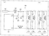
- FIG. 6 (A) of FIG. 6 is a figure which shows the structure of the general LED drive circuit 100.
- the LED drive circuit 100 includes a light emitting module 110.
- the light emitting module 110 includes light emitting lines L101 and L102 in which a plurality of light emitting elements are provided in a line, and the light emitting lines are connected in parallel to each other.
- the LED drive circuit 100 includes a general-purpose LED drive integrated circuit (IC; 101), a semiconductor switch 102, a voltage source 103, a reactance 104, a diode 105, and a capacitor 106.
- IC general-purpose LED drive integrated circuit
- the general-purpose LED drive IC 101 is connected to other components at the current input terminal ITi and the control output terminal OT to form the LED drive circuit 100.
- the general-purpose LED drive IC 101 controls the value of the current Iall flowing through the LED drive circuit 100 to a constant value (40 mA). Even if the value of the current Iall fluctuates by the control, the general-purpose LED drive IC 101 opens and closes the semiconductor switch 102 so that the value of the current Iall is maintained at the constant value.
- the LED driving circuit 100 controls several light emitting lines on the cathode side of the diode 105 by summing up the values of currents flowing through the light emitting lines.
- the number of light emitting lines, the arrangement method, the number of light emitting elements (LEDs) included in the light emitting lines, and the like can vary depending on the specifications of the general-purpose LED driving IC (for example, allowable current value, maximum number of lines, etc.). .
- the LED driving circuit 100 has the following problems.
- FIG. 6B is a diagram illustrating a state of the light emitting module 110 when the light emitting line L101 is open.
- “open” means that a part of the light emitting line is broken.
- FIG. 6B when the light emitting line L101 is open, no current flows through the light emitting line L101. That is, when the current flowing through the light emitting line L101 is I1, the value of the current I1 is 0 mA.
- the value of the current Iall flowing through the LED drive circuit 100 is controlled to a constant value (40 mA). For this reason, if the current flowing through the light emitting line L102 is I2, the value of the current I2 is 40 mA. That is, as shown in FIG. 6A, when all of the plurality of light emitting lines are operating normally, the values of the current I1 and the current I2 are 20 mA, but one of the plurality of light emitting lines is open. In some cases, a current having a double value is concentrated on the remaining light emitting lines.
- Patent Document 1 As a configuration example for improving the concentration of current to such a light emitting line, a configuration described in Patent Document 1 can be given.
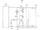
- FIG. 7 is a diagram showing a configuration of the LED drive circuit 1000 disclosed in Patent Document 1.
- the LED driving circuit 1000 one or a plurality of light emitting lines 1013 are connected in parallel to the output terminal of a constant current power source 1012 that supplies a constant current, and a bias circuit 1014 includes A constant voltage source 1015 is connected to the bias circuit 1014 in parallel.
- the base potential of the transistor 1017 is set to a predetermined potential or higher by the constant voltage source 1015.
- the LED driving circuit 1000 can be protected with a simple configuration.
- a bias circuit 1014 is connected to an external constant current power source 1012, and a current always flows even during normal driving when the light emitting line 1013 is not open. This is disadvantageous for products that require low power consumption, such as products and LED backlights.
- the present invention has been made in view of the above problems, and it is an object of the present invention to provide a circuit that can protect a light emitting line and has low power consumption.
- a circuit includes a current control element in which a plurality of light-emitting lines are connected in parallel to each other, and a total value of flowing current values is controlled to a constant value.
- a constant current line connected in parallel corresponding to each light emitting line, and each light emitting line is connected in series with the light emitting unit and the light emitting unit.
- Each of the constant current lines has a current flowing through the light emitting line when the light emitting line corresponding to the constant current line is not open.
- a constant current source that generates a current having substantially the same value as the value
- a changeover switch that is connected in series with the constant current source and switches the open state of the constant current line, Switching above When the open state detected by the detection unit provided in the light emitting line corresponding to the constant current line including the changeover switch is open, the switch is configured to turn off the constant current line. When it is not open, the constant current line is switched to open.
- a circuit according to one embodiment of the present invention is a circuit in which a plurality of light emitting lines are connected in parallel to each other, and a current control element that controls a total sum of current values flowing through the circuit to a variable target value; And a set value providing means for providing a set value to the current control element, and each light emitting line is connected in series with the light emitting unit and the light emitting unit, and detects the open state of the light emitting line.
- the setting value providing means generates the setting value corresponding to each combination of open states of the plurality of light emitting lines detected by the detection unit, and the current control element
- the target value is generated for each generated set value, and the generated target value is the light emission line when the light emission line detected as open from the value before the generation is not open.
- I a value obtained by subtracting the sum of the values of current.
- a circuit according to one embodiment of the present invention is a circuit in which a plurality of light-emitting lines are connected in parallel to each other and includes a voltage control element that controls a potential difference, and is parallel to each light-emitting line.
- Each light-emitting line includes a light-emitting unit and a detection unit that is connected in series with the light-emitting unit and detects an open state of the light-emitting line;
- Each constant current line includes a resistor having a resistance value substantially the same as the resistance value of the light emitting unit provided in the light emitting line corresponding to the constant current line, and a series connection with the resistor.
- the change-over switch that switches the open state of the constant-current line, and the change-over switch corresponds to the light-emitting line corresponding to the constant-current line that includes the change-over switch.
- the detection unit Provided is detected by the detection unit are open state, if it is open switching the constant current line to a non-open, in case a non-open switch to open the constant current line.
- FIG. 1 shows the structure of the LED drive circuit which concerns on one Embodiment of this invention. It is a figure which shows the structure of the open detection circuit with which the LED drive circuit shown in FIG. 1 is provided. It is a figure which shows the structure of the LED drive circuit which concerns on other embodiment of this invention. It is a figure which shows the structure which concerns on the modification of the setting value provision part with which the LED drive circuit shown in FIG. 3 is provided. It is a figure which shows the structure of the LED drive circuit which concerns on other embodiment of this invention. It is a figure which shows the structure of a general LED drive circuit, (a) is a figure which shows the case where all the light emission lines are normal, and (b) is the figure which shows the case where one of the light emission lines is abnormal. It is a figure which shows the structure of the LED drive circuit currently disclosed by patent document 1.
- FIG. 1 shows the structure of the open detection circuit with which the LED drive circuit shown in FIG. 1 is provided. It is a figure which shows the structure of the LED drive circuit which concerns on other
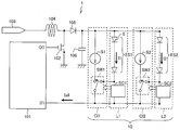
- FIG. 1 is a diagram showing a configuration of a light emitting diode (LED) drive circuit (circuit) 1 according to an embodiment of the present invention.
- the LED drive circuit 1 includes a light emitting module 10, a general-purpose LED drive integrated circuit (IC) (current control element) 101, a semiconductor switch 102, a voltage source 103, a reactance 104, and the like.
- the diode 105 and the capacitor 106 are provided.
- the general-purpose LED drive IC 101 is a current control element that controls the sum of the values of currents flowing through the LED drive circuit 1 (the value of the current Iall) to a constant value.
- the general-purpose LED drive IC 101 includes a current input terminal ITi and a control output terminal OT, and is connected to other components at each terminal.
- the LED drive circuit 1 collects several light emitting lines on the cathode side of the diode 105 (light emitting line L1, light emitting line L2), and controls the sum of the values of currents flowing through the respective light emitting lines to a constant value.
- the number of light emitting lines, the arrangement method, the number of light emitting elements E included in the light emitting lines, and the like may vary depending on the specifications of the general-purpose LED drive IC 101 (for example, allowable current value, maximum number of lines, etc.).
- the light emitting line L1 and the light emitting line L2 are connected in parallel to each other, and the light emitting module 10 is a module in which the plurality of light emitting lines are collected.
- the present invention is not limited to this configuration, and three or more light emitting lines may be combined into the light emitting module 10. That is, it can be said that the LED drive circuit 1 is an LED drive circuit in which a plurality of light emission lines (light emission line L1, light emission line L2) are connected in parallel to each other.
- Each light emitting line is connected in series with a light emitting unit (light emitting unit ES1, light emitting unit ES2) in which a plurality of light emitting elements E are collected, and an open detection for detecting the open state of the light emitting line.
- Circuit detection unit
- open detection circuit SC1 open detection circuit SC2
- the light emitting element E may be a light emitting element such as an LED, but is not limited to this configuration, and may be any light emitting element that emits light when a current flows.
- the open state means an electrical connection state in an electric circuit such as a light emitting line (light emitting line L1, light emitting line L2).
- the open state being “open” means that a part of the electric circuit is not electrically connected and current cannot flow through the electric circuit.
- the light emitting line (light emitting line L1, light emitting line L2) may be open when the light emitting unit (light emitting unit ES1, light emitting unit ES2) is abnormal due to damage or the like.
- the open state being “non-open” means that a current can flow in the electric circuit.
- the light emitting lines (light emitting line L1, light emitting line L2) can be in an open state when the light emitting units (light emitting unit ES1, light emitting unit ES2) are functioning normally.
- Constant current line CI1 and Constant current line CI2 are connected in parallel corresponding to each light emitting line.
- Each constant current line has substantially the same value as the current flowing through the light emitting line when the light emitting line (light emitting line L1, light emitting line L2) corresponding to the constant current line is not open.
- a constant current source (constant current source S1, constant current source S2) that generates the current that it has, and a changeover switch (switching) that is connected in series with the constant current source and switches the open state of the constant current line Switch SW1 and changeover switch SW2), and the changeover switch corresponds to the light emission line (constant currentization line CI1, constant currentization line CI2) and the light emitting line (the constant currentization line CI2) including the changeover switch.
- the open detection circuits (open detection circuit SC1, open detection circuit SC2) provided in the light emission line L1 and the light emission line L2) are detected. Pung state, switching to the non-open the constant current line in the case is open, when a non-open switch to open the constant current line.
- the open state may further mean an electrical connection state in an electric circuit such as a constant current line (constant current source S1, constant current source S2).
- the constant current lines are opened when a part of the electric circuit is opened by the changeover switches (changeover switch SW1, changeover switch SW2).
- the state can be open.
- constant current lines are opened when a part of the electric circuit is closed by the changeover switches (changeover switch SW1, changeover switch SW2).
- changeover switch SW1 changeover switch SW2
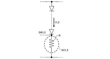
- FIG. 2 is a diagram showing the configuration of the open detection circuit SC1 and the open detection circuit SC2 provided in the LED drive circuit 1 shown in FIG.
- each open detection circuit includes a resistor R connected in series to the light emitting line (light emitting line L1, light emitting line L2), and when there is no voltage drop in the resistor, If the light emitting line (light emitting line L1, light emitting line L2) provided with an open detection circuit is open, it is detected that the light emitting line is not open when there is a voltage drop.
- the open detection circuit SC1 and the open detection circuit SC2 are connected to the cathode side of the light emitting unit ES1 and the light emitting unit ES2, but are not limited to this configuration and are connected to the anode side. May be.
- the changeover switch SW1 and the changeover switch SW2 are connected to the cathode side of the constant current source S1 and the constant current source S2, but are not limited to this configuration, and are connected to the anode side. May be.
- the open state of the light emission lines (light emission line L1, light emission line L2) can be detected by the open detection circuit (open detection circuit SC1, open detection circuit SC2) having a simple configuration including the resistor R. .
- a low-cost LED drive circuit can be provided.
- the changeover switch SW1 and the changeover switch SW2 are connected in series with a constant current source (constant current source S1 and constant current source S2), and are provided in a constant current line (constant current line CI1, constant current line CI2). The open state of the constant current line is switched.
- Table 1 is a table showing the correspondence between the determination of the open state of the open detection circuit (open detection circuit SC1, open detection circuit SC2) and the state of the changeover switch (changeover switch SW1, changeover switch SW2). As shown in Table 1, when the determination of the open detection circuit is non-open (normal), the changeover switch is turned off, and a constant current line (constant current line CI1, constant current line) including the change switch is provided. Open CI2). When the determination of the open detection circuit is open, the changeover switch is turned on and the constant current line provided with the changeover switch is not opened.
- the LED drive circuit 1 has a plurality of light emitting lines (light emitting line L1 and light emitting line L2) connected in parallel to each other, and controls the sum of the values of the flowing current (the value of the current Iall) to a constant value.
- the LED driving circuit includes a general-purpose LED driving IC 101 that includes constant current lines (constant current lines CI1, constant current lines CI2) connected in parallel corresponding to the respective light emitting lines.
- Each light emitting line is connected to a light emitting unit (light emitting unit ES1, light emitting unit ES2) in series with the light emitting unit, and an open detection circuit (open detection circuit SC1, open detection) that detects the open state of the light emitting line.
- Each constant current line is connected to the light emission line when the light emission line corresponding to the constant current line is not open.
- a constant current source (constant current source S1, constant current source S2) that generates a current having substantially the same value as the value of the current flowing through the current source, and is connected in series with the constant current source.
- Changeover switches (changeover switch SW1 and changeover switch SW2) for switching the open state of the currentization line, and the changeover switch includes the constant currentization line (constant currentization line CI1, constant current switch) including the changeover switch.
- the open state detected by the open detection circuit (open detection circuit SC1, open detection circuit SC2) provided in the light emission line (light emission line L1, light emission line L2) corresponding to the current line CI2) is open. In some cases, the constant current line is switched to non-open, and in other cases, the constant current line is switched to open. .
- the current flowing through the constant current line is the value of the current flowing through the light emitting line when the light emitting line (light emitting line L1, light emitting line L2) corresponding to the constant current line is not open. They have almost the same value.
- LED drive circuit 1 is supplied from line CI1, constant current line CI2).
- the LED drive circuit 1 does not include a constant current line (constant current line CI1, constant current line CI2), any one of the plurality of light emission lines (light emission line L1, light emission line L2)
- constant current line CI1, constant current line CI2 any one of the plurality of light emission lines
- the sum of the values of the current flowing through the LED drive circuit 1 decreases, but current control is performed by the general-purpose LED drive IC 101, and the sum is returned to the original value.
- the light emitting line that is open does not pass current, excessive current concentrates on the remaining light emitting lines that are not open, which may destroy the light emitting line.
- the LED drive circuit 1 includes the above-described constant current lines (constant current line CI1, constant current line CI2), the light emitting lines (light emitting line L1, light emitting line L2) are protected from the destruction. be able to.
- the LED drive circuit 1 in which the value of the flowing current is controlled, it is possible to provide the LED drive circuit 1 that can protect the light emitting line and has low power consumption.
- Table 2 shows the values of the currents I1 and I2 flowing through the light emitting lines L1 and L2, and the constant current sources S1 and S2 provided in the constant current lines CI1 and constant current lines CI2. It is a table
- surface which shows the value of an electric current, and the value of these electric current sum totals. As shown in Table 2, during normal operation, the values of current I1 and current I2 flowing through each light emitting line are 20 mA, and the values of the currents supplied by constant current source S1 and constant current source S2 are 0 mA. The value of the total current is 40 mA.
- the value of the current I1 is 0 mA.
- a current having a value of 20 mA is supplied from the constant current source S1 provided in the constant current line CI1 corresponding to the light emitting line L1.
- the sum of the value of the current I1 flowing through the light emitting line L1 and the value of the current supplied from the constant current source S1 provided in the constant current line CI1 corresponding to the light emitting line L1 is 20 mA as in the normal state.
- the value of the current I2 flowing through the light emitting line L2 and the value of the current supplied from the constant current source S2 provided in the constant current line CI2 do not change. Therefore, the total current is 40 mA as in the normal state.
- the value of the current I2 is 0 mA.
- a current having a value of 20 mA is supplied from the constant current source S2 provided in the constant current line CI2 corresponding to the light emitting line L2.
- the sum of the value of the current I2 flowing through the light emitting line L2 and the value of the current supplied from the constant current source S2 provided in the constant current line CI2 corresponding to the light emitting line L2 is 20 mA as in the normal state.
- the value of the current I1 flowing through the light emitting line L1 and the value of the current supplied from the constant current source S1 provided in the constant current line CI1 do not change. Therefore, the total current is 40 mA as in the normal state.
- the value of the current Iall flowing through the LED drive circuit 1 is maintained at a constant value.
- the LED drive circuit 1 according to the present embodiment is less consumed than the LED drive circuit 1000 according to the prior art described in Patent Document 1 by comparing the prior art described in Patent Document 1 and this embodiment. The power will be described.
- Table 3 is a table showing a comparison between the conventional technique described in Patent Document 1 and the present embodiment.
- the LED drive circuit 1000 includes only two rows of light emitting lines 1013, the current I1 flows through one light emitting line, and the current flows through the other light emitting line. Compared with the LED drive circuit 1 according to the present embodiment, I2 is flowing.
- the current required for making a constant current is equal to one line of light emitting lines regardless of whether one of the light emitting lines (light emitting line 1013) is open or not open. 1 mA is required, and a total current of 42 mA flows in the LED drive circuit 1000. That is, the current value that is originally required is 40 mA, and a wasteful current of 2 mA always flows.
- any of the plurality of light emission lines (light emission line L1, light emission line L2) is open.
- the constant current line CI1 is not open.
- a current having substantially the same value as that of the current flowing through the light emitting line L1 during normal operation is supplied from the constant current source S1 to the constant current line CI1. That is, even in such a case, in the present embodiment, no wasteful current flows.
- the LED drive circuit 1 according to the present embodiment does not use unnecessary current as compared with the LED drive circuit 1000 according to the related art described in Patent Document 1, and thus LED drive that can achieve lower power consumption. It can be said that it is a circuit.
- a low-cost LED drive circuit can be provided.
- an LED drive circuit capable of protecting the light emitting line and having low power consumption can be realized by using a general-purpose LED drive IC. Thereby, the cost of the LED drive circuit can be further reduced.
- FIG. 3 is a diagram showing a configuration of an LED drive circuit (circuit) 2 according to another embodiment of the present invention.
- the LED drive circuit 2 includes a general-purpose LED drive IC 101, a semiconductor switch 102, a voltage source 103, a reactance 104, a diode 105, and a capacitor 106, similar to the LED drive circuit 1. ing.
- the LED drive circuit 2 includes the light emitting module 10a instead of the light emitting module 10, and includes a setting value providing unit 22a (setting value providing means), and the general-purpose LED driving IC 101 includes a resistance input terminal ITr. The point is different from the LED drive circuit 1.
- the general-purpose LED drive IC 101 controls the sum of the values of the current flowing through the LED drive circuit 2 (the value of the current Iall) to a variable target value.
- the light emitting module 10a does not include a constant current line corresponding to the light emitting line L1 and the light emitting line L2.
- the open detection circuit SC1 and the open detection circuit SC2 are connected to the set value providing unit 22a.
- the set value providing unit 22a provides a set value to the general-purpose LED drive IC 101.
- the set value providing unit 22a changes the set value based on the open state of the light emitting line L1 and the light emitting line L2 detected by the open detecting circuit SC1 and the open detecting circuit SC2.
- change the setting value based on the open state means that the setting value corresponding to each combination of the open state is generated.
- circuit configuration resistance value
- a resistance value (100 k ⁇ ) corresponding to a combination in which one of the open states of the light emitting line L1 and the light emitting line L2 is open is generated.
- the present invention is not limited to such a configuration, and when the number of open detection circuits increases, the number of combinations increases, and the number of resistance values as corresponding setting values also increases. good.
- the general-purpose LED drive IC 101 changes the target value based on the changed set value.
- the changed target value is a value obtained by subtracting the sum of the values of the currents flowing through the light emitting lines when the light emitting lines detected to be open are not open from the values before the changes. It has been changed to be.
- change the target value based on the set value means that the target value corresponding to each set value is generated.
- total current as a target value corresponding to each “circuit configuration (resistance value)” described in Table 5 described later is generated.
- the present invention is not limited to such a configuration.
- the number of open detection circuits increases, the number of set values increases, and the number of currents corresponding to the target value also increases. Also good.
- the set value providing unit 22a includes a plurality of resistors (resistors R1 and R2) and a changeover switch SW that switches and combines the plurality of resistors.
- the changeover switch SW is switched based on the open state detected by the open detection circuit SC1 and the open detection circuit SC2.
- the set value is given as a resistance value of the set value providing unit 22a.
- switching based on the open state means switching corresponding to each combination of the open states.
- the changeover switch SW is switched to the state of the “changeover switch” corresponding to each “determination of the detection circuit” described in Table 5 described later.
- the present invention is not limited to such a configuration, and when the number of open detection circuits is increased, the number of combinations described above may be increased, and the number of changeover switches may be increased accordingly.
- the state of the changeover switch may mean a combination of the state of each changeover switch.
- the open detection circuit SC1 and the open detection circuit SC2 detect the setting value providing unit 22a having a simple configuration in which a plurality of resistors (resistors R1 and R2) are combined by the changeover switch SW.
- a desired resistance value based on the opened state can be provided as a set value to the general-purpose LED driving IC 101 via the resistance input terminal ITr.
- the set value providing unit 22a can be reduced in cost.
- a low-cost LED drive circuit can be provided.
- Table 4 shows the resistance value provided to the general-purpose LED drive IC 101 by the set value providing unit 22a and the value (total current) of the current Iall that flows in the LED drive circuit 2 when the general-purpose LED drive IC 101 controls according to the resistance value. It is a table
- the general-purpose LED drive IC 101 when the resistance value provided to the general-purpose LED drive IC 101 by the set value providing unit 22a is 100 k ⁇ , the general-purpose LED drive IC 101 is connected to the LED drive circuit 2 so that the total current is 20 mA. The value of the flowing current Iall is controlled. In addition, when the resistance value is 50 k ⁇ , the general-purpose LED drive IC 101 controls the value of the current Iall flowing through the LED drive circuit 2 so that the total current becomes 40 mA.
- Table 5 is a table showing a specific circuit configuration example of the changeover switch SW and the resistors R1 and R2 when the set value providing unit 22a provides the resistance values shown in Table 4.
- the changeover switch SW Turn on.
- the resistor R1 and the resistor R2 are connected in parallel, and a resistance value of 50 k ⁇ is input (provided) to the resistor input terminal ITr of the general-purpose LED drive IC 101.
- the changeover switch SW is turned off.
- the resistor R1 is connected to the resistor input terminal of the general-purpose LED drive IC 101, and a resistance value of 100 k ⁇ is input.
- resistance values are not limited to this configuration, and based on the specifications of the general-purpose LED drive IC 101 and the number of open detection circuits (open detection circuits SC1, open detection circuits SC2), the resistance values of the respective resistors.
- the number of resistors, the number of changeover switches, and the circuit configuration may be changed.
- the set value providing unit 22a may be configured to use software instead of the configuration using the hard air such as the resistor R1, the resistor R2, and the changeover switch SW.
- the setting value provision part 22b (setting value provision means) which is a modification of the setting value provision part 22a using software is demonstrated in detail.
- FIG. 4 is a diagram illustrating a configuration of a set value providing unit 22b which is a modification of the set value providing unit 22a provided in the LED drive circuit 2 illustrated in FIG.
- the setting value providing unit 22 b includes a conversion unit 221 (conversion unit), a memory 222, a communication unit 223, and an input unit 224.
- the memory 222 stores a conversion table D from the open state detected by the open detection circuit SC1 and the open detection circuit SC2 to the set value to be provided to the general-purpose LED drive IC 101 via the resistance input terminal ITr. .
- the conversion unit 221 converts the open state detected by the open detection circuit SC1 and the open detection circuit SC2 into the set value.
- the conversion table D is a table in which the correspondence between the open state detected by the open detection circuit (open detection circuit SC1, open detection circuit SC2) and the set value is described.
- the open state “normal (all open states are not open)” of the open detection circuit and the resistance value “50 k ⁇ ” as the set value is described, and the conversion unit 221 reads this description.
- the open state is converted into the set value.
- the open state “one of the lines (light emission line L1, light emission line L2) is open” of the open detection circuit and the resistance value “100 k ⁇ ” as a set value is described. By reading this description, the open state is converted into the set value.
- the conversion unit 221 refers to the conversion table D and converts the open state detected by the open detection circuit (open detection circuit SC1, open detection circuit SC2) into the set value.
- the conversion unit 221 converts the open state of the light emission line L1 and the light emission line L2 detected by the open detection circuit SC1 and the open detection circuit SC2 into a set value by the conversion table D as described above.
- the set value providing unit 22b can provide the general-purpose LED driving IC 101 with a set value based on the open state of the light emitting line L1 and the light emitting line L2 detected by the open detecting circuit SC1 and the open detecting circuit SC2. .
- the set value providing unit 22b can provide the set value at high speed.
- LED driving circuit capable of protecting the light emitting lines (light emitting line L1, light emitting line L2) at high speed.
- the setting value providing unit 22b is configured by hardware (for example, a resistor and a changeover switch), and the specification of the general-purpose LED drive IC 101 is changed, the hardware is changed according to the specification change. There is a possibility that an operation such as replacement of constituent parts may be required.
- the set value providing unit 22b described above can cope with the specification change by a simpler operation such as updating the conversion table D by communication by the communication unit 223 or direct input by the input unit 224, for example.
- the set value may be a value representing a resistance value.
- a current control terminal based on a resistance value is provided, and it may be necessary to input (provide) a set value based on the resistance value.
- the set value providing unit 22b can appropriately provide the set value even when the general-purpose LED drive IC 101 needs to provide the set value based on the resistance value.
- an LED drive circuit that can use a general-purpose current control element can be provided.
- the LED drive circuit 2 is an LED drive circuit in which a plurality of light emission lines (light emission line L1 and light emission line L2) are connected in parallel to each other, and the sum of the values of currents flowing through the LED drive circuit 2 is as follows.
- a general-purpose LED drive IC 101 that controls (the value of the current Iall) to a variable target value, and a set value providing unit (a set value providing unit 22a and a set value providing unit 22b) that provides the general LED drive IC 101 with a set value.
- Each light emitting line is connected to a light emitting unit (light emitting unit ES1, light emitting unit ES2) and the light emitting unit in series, and an open detection circuit (open detection circuit SC1, Open detection circuit SC2), and the set value providing unit opens the light emission line L1 and the light emission line L2 detected by the open detection circuit.
- the general-purpose LED drive IC 101 generates the target value for each of the generated set values, and the generated target value is a value before the generation. From this, it is a value obtained by subtracting the sum of the values of the currents flowing through the light emitting lines when the light emitting lines detected to be open are not open.
- each open detection circuit includes a resistor R connected in series to the light emitting lines (light emitting line L1, light emitting line L2).
- the light emitting line (light emitting line L1, light emitting line L2) provided with the open detection circuit is open, and if there is a voltage drop, the light emitting line is not open. You may detect that there is.
- the open detection circuit SC1 and the open detection circuit SC2 are connected to the cathode side of the light emitting unit ES1 and the light emitting unit ES2, but are not limited to this configuration and are connected to the anode side. May be.
- the open state of the light emission lines (light emission line L1, light emission line L2) can be detected by the open detection circuit (open detection circuit SC1, open detection circuit SC2) having a simple configuration including the resistor R. .
- the LED drive circuit 2 may include the set value providing unit 22b having the configuration shown in FIG. 4 and the open detection circuits (open detection circuit SC1 and open detection circuit SC2) having the configuration shown in FIG.
- ⁇ Operation of LED drive circuit 2> when the light emitting line (light emitting line L1, light emitting line L2) is open, no current flows through the light emitting line. Then, the open detection circuit (open detection circuit SC1, open detection circuit SC2) provided in the light emission line detects that the light emission line is open.
- the set value providing unit (the set value providing unit 22a and the set value providing unit 22b) generates a set value corresponding to each combination of the detected open states of the light emitting lines.
- the general-purpose LED drive IC 101 generates a target value based on the generated set value.
- the generated target value is a value obtained by subtracting the sum of the values of the currents flowing through the light emitting lines when the light emitting lines detected to be open are not open from the values before the generation. is there.
- the target value becomes smaller as the sum of the values of the current flowing through the LED drive circuit 2 (the value of the current Iall) decreases.
- any one of the plurality of light emitting lines (light emitting line L1, light emitting line L2) is open, the sum of the values of current flowing through the LED drive circuit 2 (the value of current Iall) decreases.
- the sum is smaller than the target value, current control is performed by the general-purpose LED drive IC 101, and the sum is returned to the original value.
- the light emitting line that is open does not pass current, excessive current concentrates on the remaining light emitting lines that are not open, which may destroy the light emitting line.
- the light emitting lines (light emitting line L1, light emitting line L2) can be protected from the destruction.
- the LED driving circuit in which the value of the flowing current is controlled it is possible to provide an LED driving circuit that can protect the light emitting line and has low power consumption.
- Table 6 is a table showing the value of the current I1 flowing through the light emitting line L1 of the LED drive circuit 2, the value of the current I2 flowing through the light emitting line L2, and the sum (current total) of the values of the current I1 and the current I2. As shown in Table 6, when the light emitting line L1 and the light emitting line L2 are not open, the value of the current I1 is 20 mA and the value of the current I2 is 20 mA. Therefore, the total current is 40 mA.
- the value of the current Iall flowing through the LED drive circuit 2 is the sum of the value of the current I1 and the value of the current I2. That is, the current Iall flowing through the LED drive circuit 2 is controlled to be a constant value of 20 mA.
- the value of the current I2 becomes 0 mA. Since the light emitting line L1 is not open, the value of the current I1 is 20 mA. That is, the current Iall flowing through the LED drive circuit 2 is controlled to be a constant value of 20 mA.
- the LED drive circuit 2 is controlled so that the current flowing through the non-open light emitting line becomes a constant value (20 mA).
- ⁇ Effect of LED drive circuit 2> it is possible to provide an LED drive circuit that can protect a light emitting line and has low power consumption in a circuit in which the value of a flowing current is controlled.
- a low-cost LED drive circuit can be provided.
- an LED drive circuit that can be easily handled can be provided.
- an LED drive circuit that can use a general-purpose LED drive IC.
- FIG. 5 is a diagram showing a configuration of an LED drive circuit (circuit) 3 according to another embodiment of the present invention. As shown in FIG. 5, the LED drive circuit 3 includes a light emitting module 10 as with the LED drive circuit 1.
- the LED drive circuit 3 includes a general-purpose LED drive IC (voltage control element) 101a instead of the general-purpose LED drive IC 101, and the general-purpose LED drive IC 101a includes a dimming (voltage dimming) terminal ITv. This is different from the LED drive circuit 1.
- the general-purpose LED drive IC 101a is a voltage control element that controls the potential difference V of the LED drive circuit 3.
- the general-purpose LED drive IC 101a includes a dimming terminal ITv and a control output terminal OT, and is connected to other components at each terminal.
- the constant current line CI1 and the constant current line CI2 are the light emitting parts (light emitting part ES1, light emitting part ES2) provided in the light emitting lines (light emitting line L1 and light emitting line L2) corresponding to the constant current line CI1 and constant current line CI2, respectively.
- resistors SR1, SR2 having substantially the same resistance value as the above.
- the LED driving circuit 3 includes a plurality of light emitting lines (light emitting line L1, light emitting line L1) connected in parallel to each other, and an LED drive having a voltage control element (general purpose LED drive IC 101a) for controlling the potential difference V.
- a constant current line (constant current line CI1, constant current line CI2) connected in parallel corresponding to each light emitting line, and each light emitting line includes a light emitting unit (light emitting).
- the constant current line has a resistance value substantially the same as the resistance value of the light emitting unit provided in the light emitting line corresponding to the constant current line.
- Resistors resistors SR1, SR2 connected in series with the resistors and a changeover switch (changeover switch SW1, changeover switch SW2) for switching the open state of the constant current line.
- each open detection circuit includes a resistor R connected in series to the light emitting lines (light emitting line L1, light emitting line L2).
- the light emitting line (light emitting line L1, light emitting line L2) provided with the open detection circuit is open, and if there is a voltage drop, the light emitting line is not open. You may detect that there is.
- the open detection circuit SC1 and the open detection circuit SC2 are connected to the cathode side of the light emitting unit ES1 and the light emitting unit ES2, but are not limited to this configuration and are connected to the anode side. May be.
- the open state of the light emission lines (light emission line L1, light emission line L2) can be detected by the open detection circuit (open detection circuit SC1, open detection circuit SC2) having a simple configuration including the resistor R. .
- the resistance is substantially the same as the resistance value of the light emitting part (light emitting part ES1, light emitting part ES2) provided in the light emitting line (light emitting line L1, light emitting line L2) corresponding to the constant current line.
- the resistance value is as follows. Thereby, the current flowing through the constant current line is the value of the current flowing through the light emitting line when the light emitting line (light emitting line L1, light emitting line L2) corresponding to the constant current line is not open. They have almost the same value.
- the LED drive circuit 3 does not include a constant current line (constant current line CI1, constant current line CI2), any one of the plurality of light emission lines (light emission line L1, light emission line L2) If it is open, the sum of the values of the current flowing through the LED drive circuit 3 (the value of the current Iall) decreases.
- the general-purpose LED drive IC 101a is a voltage control element, unlike the current control element, it does not monitor the value of the current flowing through the LED drive circuit 3, and is normal due to a change in the current value. Operation may be hindered. Moreover, this may destroy the light emitting lines (light emitting line L1, light emitting line L2).
- the LED drive circuit 3 includes the above-described constant current lines (constant current line CI1, constant current line CI2), the value of the current flowing through the LED drive circuit 3 even if current control is not performed. (The value of the current Iall) can be maintained at a substantially constant value, and the light emitting lines (light emitting line L1, light emitting line L2) can be protected from the destruction.
- a low-cost LED drive circuit can be provided.
- a circuit according to an embodiment of the present invention includes a plurality of light-emitting lines connected in parallel to each other, and a current control element (general-purpose LED driving IC 101) that controls a total sum of flowing current values to a constant value.
- a constant current line connected in parallel corresponding to each light emitting line, each light emitting line being connected in series with the light emitting part
- a detection unit for detecting the open state of the light emission line, and each constant current line corresponds to the constant current line.
- a change-over switch that switches an in-open state, and the change-over switch is detected by the detection unit provided in the light-emitting line corresponding to the constant current line including the change-over switch.
- the constant current line is switched to non-open, and when the state is not open, the constant current line is switched to open.
- the open state means an electrical connection state in an electric circuit such as a light emitting line or a constant current line.
- the open state being “open” means that a part of the electric circuit is not electrically connected and current cannot flow through the electric circuit.
- the open state of the light emitting line may be open when an abnormality has occurred due to damage to the light emitting unit or the like. Further, for example, when a part of the electric circuit of the constant current line is opened by the changeover switch, the open state can be opened.
- the open state being “non-open” means that a current can flow in the electric circuit.
- the open state of the light emitting line may become non-open when the light emitting unit functions normally.
- the open state can become non-open.
- the detection part with which the said light emission line is equipped detects that the said light emission line is open, and the said constant current is carried out by the changeover switch with which the constant current line corresponding to the said light emission line is equipped.
- the conversion line is switched to non-open. Thereby, a current is supplied from the constant current source provided in the constant current line, and the current flows through the constant current line.
- the current flowing through the constant current line has substantially the same value as the current flowing through the light emitting line when the light emitting line corresponding to the constant current line is not open. .
- the value of the current generated by the constant current source varies depending on the aging of the components constituting the circuit and the environment in which the circuit is placed (here, the environment may be, for example, temperature or humidity). Can do. However, if the value of the current does not exceed the absolute maximum rating value of the current of the light emitting unit included in the light emitting line, or the light emitting line does not break, the fluctuation can be allowed. It can be said that the values are almost the same.
- the circuit does not have a constant current line, if any of the plurality of light emitting lines is open, the sum of the values of the current flowing through the circuit is reduced. Control is performed and the sum is returned to the original value.
- the light emitting line that is open does not pass current, excessive current concentrates on the remaining light emitting lines that are not open, which may destroy the light emitting line.
- the circuit includes the above-described constant current line, the light emitting line can be protected from the destruction.
- the corresponding constant current line is open, so that no power is consumed other than the light emission in the light emitting unit.
- a circuit according to one embodiment of the present invention is a circuit in which a plurality of light emitting lines are connected in parallel to each other, and the sum of the values of currents flowing through the circuit is set to a variable target value.
- a current control element to be controlled, and set value providing means (a set value providing unit 22a and a set value providing unit 22b) for providing a set value to the current control element, and each light emitting line includes a light emitting unit, And a detection unit that detects an open state of the light emitting line, and the setting value providing means is configured to detect the open state of the plurality of light emitting lines detected by the detection unit.
- Is open Detected emission lines is a value obtained by subtracting the sum of the value of the current flowing through the light emitting line if it is not open.
- the detection part with which the said light emission line is equipped detects that the said light emission line is open.
- the set value providing means changes the set value based on the detected open state of the light emitting line.
- the current control element changes the target value based on the changed set value.
- the changed target value is a value obtained by subtracting the sum of the values of the currents flowing through the light emitting line when the light emitting line detected as open is not open from the value before the change. is there.
- the target value becomes smaller as the sum of the current values flowing through the circuit decreases.
- the sum of the current values flowing through the circuit is lowered.
- the sum is smaller than the target value, current control is performed by the current control element, and the sum is returned to the original value.
- the light emitting line that is open does not pass current, excessive current concentrates on the remaining light emitting lines that are not open, which may destroy the light emitting line.
- the light emitting line can be protected from the destruction.
- the set value providing unit includes a plurality of resistors and a changeover switch that switches and combines the plurality of resistors, and the changeover switch is detected by the detection unit.
- the set value may be a resistance value of the set value providing means.
- the set value may be switched for each combination of the open states of the plurality of light emitting lines.
- a desired resistance value based on the open state detected by the detection unit is provided as a set value to the current control element by the setting value providing unit having a simple configuration in which a plurality of resistors are combined by the changeover switch. can do.
- the set value providing means can be reduced in cost.
- a low-cost circuit can be provided.
- the setting value providing unit includes a memory storing a conversion table that describes correspondence between the open state detected by the detection unit and the setting value; You may provide the conversion means (conversion part 221) which refers to the said conversion table and converts the open state detected by the said detection part into the said setting value.
- the conversion unit converts the open state of the light emitting line detected by the detection unit into a set value using the conversion table.
- the set value providing means can provide the current control element with a set value based on the open state of the light emitting line detected by the detector.
- the set value providing means can provide the set value at high speed.
- the setting value providing means is configured by hardware (for example, a resistor and a changeover switch), and the specification of the current control element is changed, the hardware is configured according to the specification change. There is a possibility that work such as replacement of parts may be required.
- the setting value providing means described above can cope with the specification change by simpler work such as communication or updating the conversion table by direct input.
- the set value may be a value representing a resistance value.
- a general-purpose current control element for example, an LED driving IC
- a current control terminal based on a resistance value, and may require input (provide) a set value based on the resistance value.
- the set value providing means can appropriately provide the set value even when the current control element needs to provide the set value by the resistance value.
- a circuit according to one embodiment of the present invention includes a plurality of light-emitting lines connected in parallel to each other and a voltage control element (general-purpose LED driving IC 101a) that controls a potential difference.
- a constant current line connected in parallel corresponding to each light emitting line, each light emitting line is connected in series with the light emitting part and the light emitting part, and the light emitting line is opened.
- Each constant current line has a resistance value substantially the same as the resistance value of the light emitting part provided in the light emitting line corresponding to the constant current line.
- a changeover switch that is connected in series with the resistor and switches the open state of the constant current line.
- the changeover switch includes the changeover switch.
- the detection part with which the said light emission line is equipped detects that the said light emission line is open, and the said constant current is carried out by the changeover switch with which the constant current line corresponding to the said light emission line is equipped.
- the conversion line is switched to non-open. Thereby, a potential difference is generated in the resistance provided in the constant current line, and a current flows through the constant current line.
- the resistance has a resistance value substantially the same as the resistance value of the light emitting part provided in the light emitting line corresponding to the constant current line.
- the current flowing through the constant current line has substantially the same value as the current flowing through the light emitting line when the light emitting line corresponding to the constant current line is not open. .
- substantially the same resistance value means that the resistance values are not necessarily the same. Furthermore, the resistance value may vary for some reason.
- a potential difference occurs in the resistor and the value of the current flowing through the resistor and the constant current line is determined by the aging of the component constituting the circuit or the resistor itself, the environment in which the circuit is placed (where the environment is For example, it may be temperature or humidity.
- the environment is For example, it may be temperature or humidity.
- the value of the current does not exceed the absolute maximum rating value of the current of the light emitting unit included in the light emitting line, or the light emitting line does not break, the fluctuation can be allowed. It can be said that the values are almost the same.
- the resistance value of the resistor can also allow the fluctuation.
- the circuit does not include a constant current line, if any of the plurality of light emitting lines is open, the sum of the current values flowing through the circuit decreases.
- the voltage control element does not monitor the value of the current flowing in the circuit and the normal operation may be hindered by the change in the value of the current. This may also destroy the light emitting line.
- the circuit since the circuit includes the above-described constant current line, the total sum of current values flowing through the circuit can be maintained at a substantially constant value even if current control is not performed. Can be protected.
- the corresponding constant current line is open, so that no power is consumed other than the light emission in the light emitting unit.
- a circuit that can protect a light emitting line and has low power consumption can be provided.
- the detection unit includes a resistor connected in series to the light emitting line, and includes the detection unit when there is no voltage drop in the resistor. If the light emitting line is open, it may be detected that the light emitting line is not open when the voltage drop is present.
- the open state of the light emitting line can be detected by the detection unit having a simple configuration including a resistor.
- a low-cost circuit can be provided.
- a computer can function as the conversion unit by a control program. Furthermore, the control program can be executed on a general-purpose computer by recording the control program on a computer-readable recording medium.
- the conversion unit 221 included in the setting value providing unit 22b may be realized in hardware by a logic circuit formed on an integrated circuit (IC chip) or using a CPU (Central Processing Unit). It may be realized by software.
- the setting value providing unit 22b includes a CPU that executes instructions of a program that realizes each function, a ROM (Read Memory) that stores the program, a RAM (Random Access Memory) that expands the program, and the program And a storage device (recording medium) such as a memory for storing various data.
- An object of the present invention is a recording medium in which a program code (execution format program, intermediate code program, source program) of a control program of the set value providing unit 22b, which is software that realizes the functions described above, is recorded so as to be readable by a computer. Can also be achieved by reading the program code recorded on the recording medium and executing it by the computer (or CPU or MPU).
- Examples of the recording medium include non-transitory tangible media, such as magnetic tapes and cassette tapes, magnetic disks such as floppy (registered trademark) disks / hard disks, and CD-ROM / MO.
- Discs including optical disks such as / MD / DVD / CD-R, cards such as IC cards (including memory cards) / optical cards, and semiconductor memories such as mask ROM / EPROM / EEPROM (registered trademark) / flash ROM
- logic circuits such as PLD (Programmable logic device) and FPGA (Field Programmable Gate array) can be used.
- the set value providing unit 22b may be configured to be connectable to a communication network, and the program code may be supplied via the communication network.
- the communication network is not particularly limited as long as it can transmit the program code.
- the Internet intranet, extranet, LAN, ISDN, VAN, CATV communication network, virtual private network (Virtual Private Network), telephone line network, mobile communication network, satellite communication network, etc. can be used.
- the transmission medium constituting the communication network may be any medium that can transmit the program code, and is not limited to a specific configuration or type.
- wired lines such as IEEE 1394, USB, power line carrier, cable TV line, telephone line, ADSL (Asymmetric Digital Subscriber Line) line, infrared rays such as IrDA and remote control, Bluetooth (registered trademark), IEEE 802.11 wireless, HDR ( It can also be used wirelessly such as High Data Rate, NFC (Near Field Communication), DLNA (registered trademark) (Digital Living Network Alliance), mobile phone network, satellite line, and digital terrestrial network.
- the present invention can also be realized in the form of a computer data signal embedded in a carrier wave in which the program code is embodied by electronic transmission.
- the present invention can be widely used for display devices that employ LEDs as light sources. Further, the present invention can be used for all light emitting devices that collectively drive a large number of light emitting elements.
Landscapes
- Led Devices (AREA)
Abstract
LED駆動回路(1)は発光ライン(L1)および発光ライン(L2)が接続され、電流(Iall)の値を制御する汎用LED駆動IC(101)と定電流化ライン(CI1)および定電流化ライン(CI2)とを備え、発光ライン(L1)は定電流源(S1)と切替スイッチ(SW1)とを備え、切替スイッチ(SW1)は定電流化ライン(L1)のオープン状態を切り替える。
Description
本発明は、互いに並列に接続されている複数の発光ラインを備えている回路に関する。
近年、IA(Industrial Appliance)分野で利用されるディスプレイ装置には、安全性・経済性・環境性への配慮が求められている。これを受けて、特に、液晶ディスプレイ(LCD;Liquid Crystal Display)では、バックライトの光源として発光ダイオード(LED;Light Emitting Diode)を採用することにより、従来以上の長寿命化を実現することが検討されている。
このような用途においては、複数のLEDをライン状に設け、当該ラインをさらに複数備え、多数のLEDを一括して駆動できるようにモジュール化することが行われている。
図6の(a)は、一般的なLED駆動回路100の構成を示す図である。図6の(a)に示すように、LED駆動回路100は、発光モジュール110を備えている。発光モジュール110は、複数の発光素子をライン状に設けた発光ラインL101およびL102を備えており、各発光ラインは、互いに並列に接続されている。
また、LED駆動回路100は、汎用LED駆動集積回路(IC;Integrated Circuit)101と、半導体スイッチ102と、電圧源103と、リアクタンス104と、ダイオード105と、コンデンサ106とを備えている。
ここで、汎用LED駆動IC101は、電流入力端子ITiおよび制御出力端子OTにおいて他の構成要素と接続されており、LED駆動回路100を形成している。このような構成により、汎用LED駆動IC101は、LED駆動回路100に流れる電流Iallの値を、一定値(40mA)に制御している。当該制御により、電流Iallの値が変動しても、汎用LED駆動IC101が半導体スイッチ102を開閉することで、電流Iallの値は、当該一定値に維持される。つまり、LED駆動回路100は、ダイオード105のカソード側の各発光ラインを数ラインまとめて、各発光ラインに流れる電流の値の総和により制御している。
なお、発光ラインの数、配列方式、および発光ラインに含まれる発光素子(LED)の数などは、汎用LED駆動ICの仕様(例えば、許容できる電流値、最大ライン数など)により、変化し得る。
しかしながら、LED駆動回路100には、次のような問題が存在する。
図6の(b)は、発光ラインL101がオープンである場合の発光モジュール110の状態を示す図である。ここで、「オープン」とは、発光ラインの一部が断線していることを意味している。図6の(b)に示すように、発光ラインL101がオープンである場合には、発光ラインL101に電流が流れない。つまり、発光ラインL101に流れる電流をI1としたとき、電流I1の値は0mAとなる。
ここで、上述のように、LED駆動回路100に流れる電流Iallの値は、一定値(40mA)に制御されている。このため、発光ラインL102に流れる電流をI2とすると、電流I2の値は40mAとなる。つまり、図6の(a)に示すように、複数の発光ラインがすべて正常に動作しているときには、電流I1および電流I2の値は20mAであるが、複数の発光ラインのいずれかがオープンである場合には、残りの他の発光ラインに2倍の値を有する電流が集中する。
以上のように、一般的なLED駆動回路100では、発光ラインに電流が集中し、例えば、当該発光ラインに含まれる発光素子の絶対最大定格オーバーによって、当該発光素子が破壊されるなどの懸念がある。
このような発光ラインへの電流の集中を改善する構成例として、特許文献1に記載の構成を挙げることができる。
図7は、特許文献1に開示されているLED駆動回路1000の構成を示す図である。図7に示すように、LED駆動回路1000では、一定電流を供給する定電流電源1012の出力端子に、1つ、あるいは複数の発光ライン1013が互いに並列に接続されているとともに、バイアス回路1014が並列に接続され、かつ、このバイアス回路1014に定電圧源1015が接続されている。そして、定電圧源1015により、トランジスタ1017のベース電位を所定の電位以上に設定している。また、発光ライン1013のLED1016の少なくともいずれかが破損などにより開放(オープン)した場合でも、他の発光ライン1013に接続したトランジスタ1017のベース電位の低下を定電圧源1015により防止でき、他の発光ライン1013での電流を一定に維持し、簡単な構成でLED駆動回路1000を保護できるとしている。
しかしながら、上述のような特許文献1のLED駆動回路1000には、以下の問題が存在する。
LED駆動回路1000では、外付けの定電流電源1012にバイアス回路1014が接続されており、発光ライン1013がオープンしていない正常駆動時にも、常に電流が流れる構成となっており、例えば、バッテリー駆動製品やLEDバックライトなど、低消費電力化を求められる製品では不利となる。
本発明は、上述の問題に鑑みて成されたもので、発光ラインを保護可能かつ低消費電力な回路を提供することにある。
上記の課題を解決するために、本発明の一態様に係る回路は、複数の発光ラインが互いに並列に接続されており、流れる電流の値の総和を一定値に制御する電流制御素子を備えている回路であって、各発光ラインに対応して並列に接続されている定電流化ラインを備えており、各発光ラインは、発光部と、当該発光部と直列に接続されており、当該発光ラインのオープン状態を検知する検知部とを備えており、各定電流化ラインは、当該定電流化ラインそれぞれに対応している上記発光ラインが非オープンである場合に当該発光ラインに流れる電流の値と概ね同一の値を有している電流を生起する定電流源と、当該定電流源と直列に接続されており、当該定電流化ラインのオープン状態を切り替える切替スイッチとを備えており、上記切替スイッチは、当該切替スイッチを備えている上記定電流化ラインと対応する上記発光ラインに備えられている上記検知部により検知されたオープン状態が、オープンである場合には当該定電流化ラインを非オープンに切り替え、非オープンである場合には当該定電流化ラインをオープンに切り替える。
また、本発明の一態様に係る回路は、複数の発光ラインが互いに並列に接続されている回路であって、上記回路に流れる電流の値の総和を可変の目標値に制御する電流制御素子と、上記電流制御素子に設定値を提供する設定値提供手段とを備えており、各発光ラインは、発光部と、当該発光部と直列に接続されており、当該発光ラインのオープン状態を検知する検知部とを備えており、上記設定値提供手段は、上記検知部により検知された上記複数の発光ラインのオープン状態の組み合わせ毎に対応する上記設定値を生成し、上記電流制御素子は、当該生成された設定値毎に、上記目標値を生成し、当該生成された目標値は、当該生成より以前の値から、オープンであると検知された発光ラインが非オープンである場合に当該発光ラインに流れる電流の値の総和を減算した値である。
また、本発明の一態様に係る回路は、複数の発光ラインが互いに並列に接続されており、電位差を制御する電圧制御素子を備えている回路であって、各発光ラインに対応して並列に接続されている定電流化ラインを備えており、各発光ラインは、発光部と、当該発光部と直列に接続されており、当該発光ラインのオープン状態を検知する検知部とを備えており、各定電流化ラインは、当該定電流化ラインそれぞれに対応している上記発光ラインに備えられている上記発光部の抵抗値と概ね同一の抵抗値を有している抵抗と、当該抵抗と直列に接続されており、当該定電流化ラインのオープン状態を切り替える切替スイッチとを備えており、上記切替スイッチは、当該切替スイッチを備えている上記定電流化ラインと対応する上記発光ラインに備えられている上記検知部により検知されたオープン状態が、オープンである場合には当該定電流化ラインを非オープンに切り替え、非オープンである場合には当該定電流化ラインをオープンに切り替える。
本発明の一態様によれば、発光ラインを保護可能かつ低消費電力な回路を提供することができる効果を奏する。
以下、本発明の実施の形態について、詳細に説明する。
〔実施形態1〕
本発明の一実施形態について、図1および図2に基づいて説明すれば、以下のとおりである。
本発明の一実施形態について、図1および図2に基づいて説明すれば、以下のとおりである。
<LED駆動回路1の構成>
図1は、本発明の一実施形態に係る発光ダイオード(LED;Light Emitting Diode)駆動回路(回路)1の構成を示す図である。図1に示すように、LED駆動回路1は、発光モジュール10と、汎用LED駆動集積回路(IC;Integrated Circuit)(電流制御素子)101と、半導体スイッチ102と、電圧源103と、リアクタンス104と、ダイオード105と、コンデンサ106とを備えている。
図1は、本発明の一実施形態に係る発光ダイオード(LED;Light Emitting Diode)駆動回路(回路)1の構成を示す図である。図1に示すように、LED駆動回路1は、発光モジュール10と、汎用LED駆動集積回路(IC;Integrated Circuit)(電流制御素子)101と、半導体スイッチ102と、電圧源103と、リアクタンス104と、ダイオード105と、コンデンサ106とを備えている。
以下では、LED駆動回路1が備える主な構成要素について、詳細に説明する。
(汎用LED駆動IC101)
汎用LED駆動IC101は、LED駆動回路1に流れる電流の値の総和(電流Iallの値)を一定値に制御する電流制御素子である。
汎用LED駆動IC101は、LED駆動回路1に流れる電流の値の総和(電流Iallの値)を一定値に制御する電流制御素子である。
また、汎用LED駆動IC101は、電流入力端子ITiおよび制御出力端子OTを備えており、各端子において他の構成要素と接続されている。
また、汎用LED駆動IC101では、電流Iallの値が変動しても、汎用LED駆動IC101が半導体スイッチ102を開閉することで、電流Iallの値は、一定値に維持される。つまり、LED駆動回路1は、ダイオード105のカソード側の発光ライン(発光ラインL1、発光ラインL2)を数ラインまとめて、各発光ラインに流れる電流の値の総和を一定値に制御している。
なお、発光ラインの数、配列方式、および発光ラインに含まれる発光素子Eの数などは、汎用LED駆動IC101の仕様(例えば、許容できる電流値、最大ライン数など)により変化しても良い。
(発光ラインL1および発光ラインL2)
発光ラインL1および発光ラインL2は、互いに並列に接続されており、発光モジュール10は、当該複数の発光ラインをまとめたモジュールである。しかしながら、この構成に限定されるわけではなく、発光ラインは、3列以上をまとめて発光モジュール10としても良い。つまり、LED駆動回路1は、複数の発光ライン(発光ラインL1、発光ラインL2)が互いに並列に接続されているLED駆動回路であると言える。
発光ラインL1および発光ラインL2は、互いに並列に接続されており、発光モジュール10は、当該複数の発光ラインをまとめたモジュールである。しかしながら、この構成に限定されるわけではなく、発光ラインは、3列以上をまとめて発光モジュール10としても良い。つまり、LED駆動回路1は、複数の発光ライン(発光ラインL1、発光ラインL2)が互いに並列に接続されているLED駆動回路であると言える。
各発光ラインは、発光素子Eが複数個まとめられている発光部(発光部ES1、発光部ES2)と、当該発光部と直列に接続されており、当該発光ラインのオープン状態を検知するオープン検知回路(検知部)(オープン検知回路SC1、オープン検知回路SC2)とを備えている。
ここで、発光素子Eは、LEDなどの発光素子であっても良いが、この構成に限定されるわけではなく、電流が流れることにより発光する発光素子であれば何であっても良い。
また、オープン状態とは、発光ライン(発光ラインL1、発光ラインL2)などの電気回路における、電気的な接続状態を意味している。
また、オープン状態が「オープン」であるとは、上記電気回路の一部が電気的に接続されておらず、当該電気回路に電流が流れ得ない状態であることを意味する。例えば、発光ライン(発光ラインL1、発光ラインL2)は、発光部(発光部ES1、発光部ES2)の破損などによる異常が発生している場合には、オープン状態がオープンになり得る。
また、オープン状態が「非オープン」であるとは、上記電気回路に電流が流れ得る状態であることを意味する。例えば、発光ライン(発光ラインL1、発光ラインL2)は、発光部(発光部ES1、発光部ES2)が正常に機能している場合には、オープン状態が非オープンになり得る。
(定電流化ラインCI1および定電流化ラインCI2)
定電流化ラインCI1および定電流化ラインCI2は、各発光ラインに対応して並列に接続されている。
定電流化ラインCI1および定電流化ラインCI2は、各発光ラインに対応して並列に接続されている。
各定電流化ラインは、当該定電流化ラインそれぞれに対応している発光ライン(発光ラインL1、発光ラインL2)が非オープンである場合に当該発光ラインに流れる電流の値と概ね同一の値を有している電流を生起する定電流源(定電流源S1、定電流源S2)と、当該定電流源と直列に接続されており、当該定電流化ラインのオープン状態を切り替える切替スイッチ(切替スイッチSW1、切替スイッチSW2)とを備えており、上記切替スイッチは、当該切替スイッチを備えている上記定電流化ライン(定電流化ラインCI1、定電流化ラインCI2)と対応する上記発光ライン(発光ラインL1、発光ラインL2)に備えられている上記オープン検知回路(オープン検知回路SC1、オープン検知回路SC2)により検知されたオープン状態が、オープンである場合には当該定電流化ラインを非オープンに切り替え、非オープンである場合には当該定電流化ラインをオープンに切り替える。
また、オープン状態とは、さらに定電流化ライン(定電流源S1、定電流源S2)などの電気回路における、電気的な接続状態を意味していても良い。
また、例えば、定電流化ライン(定電流化ラインCI1、定電流化ラインCI2)は、切替スイッチ(切替スイッチSW1、切替スイッチSW2)により電気回路の一部が開かれている場合には、オープン状態がオープンになり得る。
また、例えば、定電流化ライン(定電流化ラインCI1、定電流化ラインCI2)は、切替スイッチ(切替スイッチSW1、切替スイッチSW2)により電気回路の一部が閉じられている場合には、オープン状態が非オープンになり得る。
(オープン検知回路SC1およびオープン検知回路SC2)
図2は、図1に示すLED駆動回路1が備えているオープン検知回路SC1およびオープン検知回路SC2の構成を示す図である。図2に示すように、各オープン検知回路は、発光ライン(発光ラインL1、発光ラインL2)に直列に接続されている抵抗Rを備えており、当該抵抗における電圧降下が無い場合には、当該オープン検知回路を備えている上記発光ライン(発光ラインL1、発光ラインL2)がオープンであると、当該電圧降下が有る場合には、当該発光ラインが非オープンであると検知する。
図2は、図1に示すLED駆動回路1が備えているオープン検知回路SC1およびオープン検知回路SC2の構成を示す図である。図2に示すように、各オープン検知回路は、発光ライン(発光ラインL1、発光ラインL2)に直列に接続されている抵抗Rを備えており、当該抵抗における電圧降下が無い場合には、当該オープン検知回路を備えている上記発光ライン(発光ラインL1、発光ラインL2)がオープンであると、当該電圧降下が有る場合には、当該発光ラインが非オープンであると検知する。
なお、図1では、オープン検知回路SC1およびオープン検知回路SC2は、発光部ES1および発光部ES2のカソード側に接続されているが、この構成に限定されるわけではなく、アノード側に接続されていても良い。
また、図1では、切替スイッチSW1および切替スイッチSW2は、定電流源S1および定電流源S2のカソード側に接続されているが、この構成に限定されるわけではなく、アノード側に接続されていても良い。
上記構成によれば、抵抗Rからなる簡単な構成のオープン検知回路(オープン検知回路SC1、オープン検知回路SC2)により、発光ライン(発光ラインL1、発光ラインL2)のオープン状態を検知することができる。
すなわち、低コストなLED駆動回路を提供することができる。
(切替スイッチSW1および切替スイッチSW2)
切替スイッチSW1および切替スイッチSW2は、定電流源(定電流源S1および定電流源S2)と直列に接続されて、定電流化ライン(定電流化ラインCI1、定電流化ラインCI2)に備えられており、当該定電流化ラインのオープン状態を切り替える。
切替スイッチSW1および切替スイッチSW2は、定電流源(定電流源S1および定電流源S2)と直列に接続されて、定電流化ライン(定電流化ラインCI1、定電流化ラインCI2)に備えられており、当該定電流化ラインのオープン状態を切り替える。

表1は、オープン検知回路(オープン検知回路SC1、オープン検知回路SC2)のオープン状態の判定と、切替スイッチ(切替スイッチSW1、切替スイッチSW2)の状態の対応を示す表である。表1に示すように、オープン検知回路の判定が非オープン(正常)であるときには、切替スイッチはオフとなり、当該切替スイッチを備えている定電流化ライン(定電流化ラインCI1、定電流化ラインCI2)をオープンにする。また、オープン検知回路の判定がオープンであるときには、切替スイッチはオンとなり、当該切替スイッチを備えている定電流化ラインを非オープンにする。
(LED駆動回路1の構成のまとめ)
以上のように、LED駆動回路1は、複数の発光ライン(発光ラインL1、発光ラインL2)が互いに並列に接続されており、流れる電流の値の総和(電流Iallの値)を一定値に制御する汎用LED駆動IC101を備えているLED駆動回路であって、各発光ラインに対応して並列に接続されている定電流化ライン(定電流化ラインCI1、定電流化ラインCI2)を備えており、各発光ラインは、発光部(発光部ES1、発光部ES2)と、当該発光部と直列に接続されており、当該発光ラインのオープン状態を検知するオープン検知回路(オープン検知回路SC1、オープン検知回路SC2)とを備えており、各定電流化ラインは、当該定電流化ラインそれぞれに対応している上記発光ラインが非オープンである場合に当該発光ラインに流れる電流の値と概ね同一の値を有している電流を生起する定電流源(定電流源S1、定電流源S2)と、当該定電流源と直列に接続されており、当該定電流化ラインのオープン状態を切り替える切替スイッチ(切替スイッチSW1、切替スイッチSW2)とを備えており、上記切替スイッチは、当該切替スイッチを備えている上記定電流化ライン(定電流化ラインCI1、定電流化ラインCI2)と対応する上記発光ライン(発光ラインL1、発光ラインL2)に備えられている上記オープン検知回路(オープン検知回路SC1、オープン検知回路SC2)により検知されたオープン状態が、オープンである場合には当該定電流化ラインを非オープンに切り替え、非オープンである場合には当該定電流化ラインをオープンに切り替える。
以上のように、LED駆動回路1は、複数の発光ライン(発光ラインL1、発光ラインL2)が互いに並列に接続されており、流れる電流の値の総和(電流Iallの値)を一定値に制御する汎用LED駆動IC101を備えているLED駆動回路であって、各発光ラインに対応して並列に接続されている定電流化ライン(定電流化ラインCI1、定電流化ラインCI2)を備えており、各発光ラインは、発光部(発光部ES1、発光部ES2)と、当該発光部と直列に接続されており、当該発光ラインのオープン状態を検知するオープン検知回路(オープン検知回路SC1、オープン検知回路SC2)とを備えており、各定電流化ラインは、当該定電流化ラインそれぞれに対応している上記発光ラインが非オープンである場合に当該発光ラインに流れる電流の値と概ね同一の値を有している電流を生起する定電流源(定電流源S1、定電流源S2)と、当該定電流源と直列に接続されており、当該定電流化ラインのオープン状態を切り替える切替スイッチ(切替スイッチSW1、切替スイッチSW2)とを備えており、上記切替スイッチは、当該切替スイッチを備えている上記定電流化ライン(定電流化ラインCI1、定電流化ラインCI2)と対応する上記発光ライン(発光ラインL1、発光ラインL2)に備えられている上記オープン検知回路(オープン検知回路SC1、オープン検知回路SC2)により検知されたオープン状態が、オープンである場合には当該定電流化ラインを非オープンに切り替え、非オープンである場合には当該定電流化ラインをオープンに切り替える。
<LED駆動回路1の動作>
上記構成によれば、発光ライン(発光ラインL1、発光ラインL2)がオープンである場合には、当該発光ラインに電流が流れない。そして、当該発光ラインに備えられているオープン検知回路(オープン検知回路SC1、オープン検知回路SC2)は、当該発光ラインがオープンであることを検知し、当該発光ラインに対応している定電流化ライン(定電流化ラインCI1、定電流化ラインCI2)に備えられている切替スイッチ(切替スイッチSW1、切替スイッチSW2)により、当該定電流化ラインは、非オープンに切り替えられる。これにより、当該定電流化ラインに備えられている定電流源(定電流源S1、定電流源S2)から電流(電流I1、電流I2)が供給され、当該定電流化ラインに電流が流れる。
上記構成によれば、発光ライン(発光ラインL1、発光ラインL2)がオープンである場合には、当該発光ラインに電流が流れない。そして、当該発光ラインに備えられているオープン検知回路(オープン検知回路SC1、オープン検知回路SC2)は、当該発光ラインがオープンであることを検知し、当該発光ラインに対応している定電流化ライン(定電流化ラインCI1、定電流化ラインCI2)に備えられている切替スイッチ(切替スイッチSW1、切替スイッチSW2)により、当該定電流化ラインは、非オープンに切り替えられる。これにより、当該定電流化ラインに備えられている定電流源(定電流源S1、定電流源S2)から電流(電流I1、電流I2)が供給され、当該定電流化ラインに電流が流れる。
ここで、当該定電流化ラインに流れる電流は、当該定電流化ラインと対応している発光ライン(発光ラインL1、発光ラインL2)が非オープンである場合に当該発光ラインに流れる電流の値と概ね同一の値を有している。
よって、発光ライン(発光ラインL1、発光ラインL2)がオープンであっても、当該発光ラインが非オープンである場合と概ね同一の値を有している電流が、定電流化ライン(定電流化ラインCI1、定電流化ラインCI2)からLED駆動回路1に供給される。
仮に、LED駆動回路1が定電流化ライン(定電流化ラインCI1、定電流化ラインCI2)を備えていなければ、複数の発光ライン(発光ラインL1、発光ラインL2)のいずれかの発光ラインがオープンである場合には、LED駆動回路1に流れる電流の値の総和(電流Iallの値)が低下するが、汎用LED駆動IC101により電流制御が行われ、当該総和が元の値に戻される。ここで、オープンである発光ラインは電流を流さないので、非オープンである残りの発光ラインに過大な電流が集中し、当該発光ラインが破壊される可能性がある。
しかしながら、LED駆動回路1は、上述の定電流化ライン(定電流化ラインCI1、定電流化ラインCI2)を備えているため、当該破壊から発光ライン(発光ラインL1、発光ラインL2)を保護することができる。
また、発光ライン(発光ラインL1、発光ラインL2)が非オープン(正常)である場合には、対応する定電流化ラインがオープンであるため、発光部(発光部ES1、発光部ES2)における発光以外には、何らの電力も消費されない。
すなわち、流れる電流の値が制御されているLED駆動回路において、発光ラインを保護可能かつ低消費電力なLED駆動回路1を提供することができる。
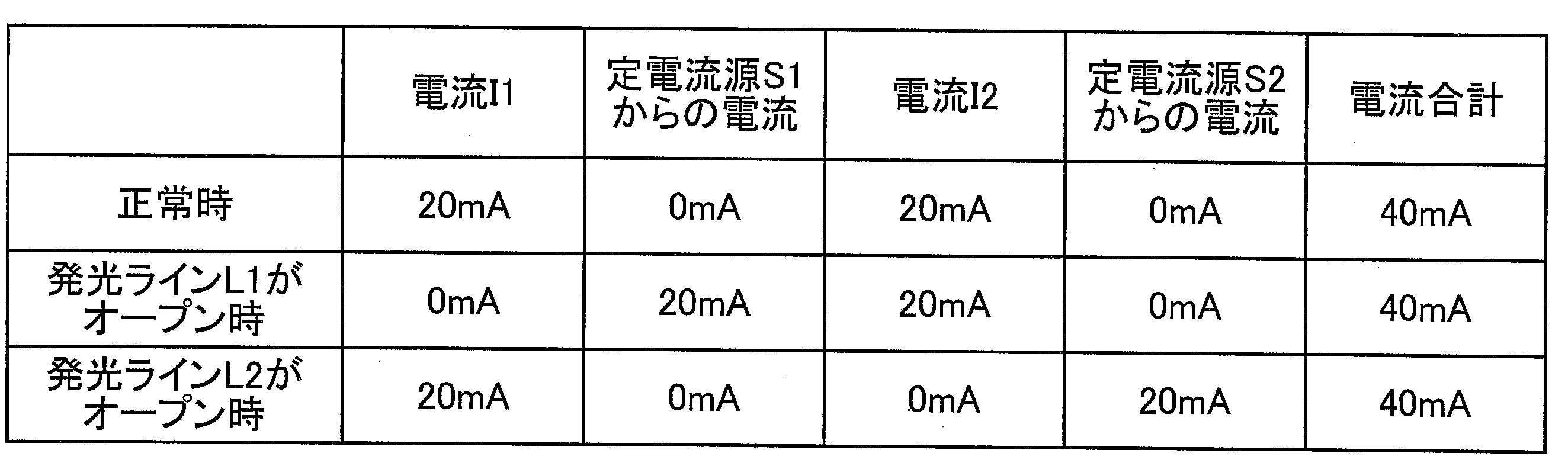
表2は、発光ラインL1および発光ラインL2に流れる電流I1および電流I2の値と、定電流化ラインCI1および定電流化ラインCI2に備えられている定電流源S1および定電流源S2が供給する電流の値と、これらの電流合計の値とを示す表である。表2に示すように、正常時には、各発光ラインに流れる電流I1および電流I2の値は、20mAであり、定電流源S1および定電流源S2が供給する電流の値は0mAである。また、これらの電流合計の値は、40mAである。
次に、発光ラインL1のオープン時には、発光ラインL1に電流が流れないため、電流I1の値は0mAである。しかしながら、発光ラインL1に対応する定電流化ラインCI1が備えている定電流源S1から20mAの値を有する電流が供給される。このため、発光ラインL1に流れる電流I1の値と、発光ラインL1に対応する定電流化ラインCI1が備えている定電流源S1から供給される電流の値の合計は、正常時と同様に20mAになる。また、発光ラインL2に流れる電流I2の値と、定電流化ラインCI2が備えている定電流源S2から供給される電流の値は変化しない。よって、電流合計は、正常時と同様に40mAとなる。
同様に、発光ラインL2のオープン時には、発光ラインL2に電流が流れないため、電流I2の値は0mAである。しかしながら、発光ラインL2に対応する定電流化ラインCI2が備えている定電流源S2から20mAの値を有する電流が供給される。このため、発光ラインL2に流れる電流I2の値と、発光ラインL2に対応する定電流化ラインCI2が備えている定電流源S2から供給される電流の値の合計は、正常時と同様に20mAになる。また、発光ラインL1に流れる電流I1の値と、定電流化ラインCI1が備えている定電流源S1から供給される電流の値は変化しない。よって、電流合計は、正常時と同様に40mAとなる。
すなわち、発光ラインL1および発光ラインL2のいずれの発光ラインがオープンである場合にも、LED駆動回路1に流れる電流Iallの値は、一定値に維持される。
以下では、特許文献1に記載の従来技術と本実施形態とを比較して、本実施形態に係るLED駆動回路1が、特許文献1に記載の従来技術に係るLED駆動回路1000よりも低消費電力であることについて説明する。
<特許文献1に記載の従来技術と本実施形態との比較>

表3は、特許文献1に記載の従来技術と本実施形態との比較を示す表である。以下では、図7に示す特許文献1に記載の従来技術において、LED駆動回路1000は、発光ライン1013を2列のみ備えており、一方の発光ラインに電流I1が流れ、他方の発光ラインに電流I2が流れているものとして、本実施形態に係るLED駆動回路1と比較する。
表3に示すように、特許文献1に記載の従来技術および本実施形態においては、1列の発光ラインあたりに20mAの値を有している電流を流す必要があり、LED駆動回路全体では、本来、合計40mAの値を有している電流を流す必要がある。
まず、特許文献1では、複数の発光ライン(発光ライン1013)のうちいずれかの発光ラインがオープンであっても、非オープンであっても、定電流化に要する電流が1列の発光ラインあたり1mA必要であり、合計42mAの電流がLED駆動回路1000に流れている。つまり、本来必要な電流の値は40mAであり、2mAの無駄な電流が常に流れている。
一方、本実施形態では、複数の発光ラインがすべて非オープンである正常時に、定電流化ラインCI1および定電流化ラインCI2はオープンとなっているため、特許文献1に記載の従来技術に係る構成とは異なり、無駄な電流が流れない。
また、本実施形態では、複数の発光ライン(発光ラインL1、発光ラインL2)のいずれかがオープンである、例えば、発光ラインL1がオープンである場合には、定電流化ラインCI1が非オープンとなり、正常時に発光ラインL1に流れていた電流の値と概ね同一の値を有する電流が、定電流源S1から定電流化ラインCI1に供給される。つまり、このような場合にも、本実施形態では、無駄な電流が流れない。
すなわち、本実施形態に係るLED駆動回路1は、特許文献1に記載の従来技術に係るLED駆動回路1000と比較して、無駄な電流が流れないため、より低消費電力化が可能なLED駆動回路であると言える。
<LED駆動回路1の効果>
本実施形態によれば、流れる電流の値が制御されているLED駆動回路において、発光ラインを保護可能かつ低消費電力なLED駆動回路を提供することができる。
本実施形態によれば、流れる電流の値が制御されているLED駆動回路において、発光ラインを保護可能かつ低消費電力なLED駆動回路を提供することができる。
また、低コストなLED駆動回路を提供することができる。
さらに、発光ラインを保護可能かつ低消費電力なLED駆動回路を、汎用のLED駆動ICを利用して実現することができる。これにより、LED駆動回路を、より低コスト化することができる。
以上では、LED駆動回路に流れる電流の値の総和を一定値に制御する実施形態について説明した。以下では、LED駆動回路に流れる電流の値の総和を可変の目標値に制御する実施形態について説明する。
〔実施形態2〕
本発明の他の実施形態について、図3および図4に基づいて説明すれば、以下のとおりである。なお、説明の便宜上、上記実施形態にて説明した図面と同一の機能を有する部材については、同一の符号を付記し、その説明を省略する。
本発明の他の実施形態について、図3および図4に基づいて説明すれば、以下のとおりである。なお、説明の便宜上、上記実施形態にて説明した図面と同一の機能を有する部材については、同一の符号を付記し、その説明を省略する。
<LED駆動回路2の構成>
図3は、本発明の他の実施形態に係るLED駆動回路(回路)2の構成を示す図である。図3に示すように、LED駆動回路2は、LED駆動回路1と同様に、汎用LED駆動IC101と、半導体スイッチ102と、電圧源103と、リアクタンス104と、ダイオード105と、コンデンサ106とを備えている。
図3は、本発明の他の実施形態に係るLED駆動回路(回路)2の構成を示す図である。図3に示すように、LED駆動回路2は、LED駆動回路1と同様に、汎用LED駆動IC101と、半導体スイッチ102と、電圧源103と、リアクタンス104と、ダイオード105と、コンデンサ106とを備えている。
しかしながら、LED駆動回路2は、発光モジュール10ではなく発光モジュール10aを備えており、設定値提供部22a(設定値提供手段)を備えており、汎用LED駆動IC101が抵抗入力端子ITrを備えている点が、LED駆動回路1とは異なっている。
また、LED駆動回路2では、汎用LED駆動IC101が、LED駆動回路2に流れる電流の値の総和(電流Iallの値)を可変の目標値に制御している。
以下では、LED駆動回路2が備える主な構成要素について、詳細に説明する。
(発光モジュール10a)
発光モジュール10aは、発光モジュール10と異なり、発光ラインL1および発光ラインL2に対応する定電流化ラインを備えていない。また、オープン検知回路SC1およびオープン検知回路SC2は、設定値提供部22aへ接続されている。
発光モジュール10aは、発光モジュール10と異なり、発光ラインL1および発光ラインL2に対応する定電流化ラインを備えていない。また、オープン検知回路SC1およびオープン検知回路SC2は、設定値提供部22aへ接続されている。
(設定値提供部22a)
設定値提供部22aは、汎用LED駆動IC101に設定値を提供する。
設定値提供部22aは、汎用LED駆動IC101に設定値を提供する。
また、設定値提供部22aは、オープン検知回路SC1およびオープン検知回路SC2により検知された発光ラインL1および発光ラインL2のオープン状態に基づいて設定値を変更する。
ここで、「オープン状態に基づいて設定値を変更する」とは、オープン状態の組み合わせ毎に対応する上記設定値を生成することを意味している。
具体的には、後述する表5に記載の「検知回路の判定」毎に対応する、設定値としての「回路構成(抵抗値)」を生成することを意味している。
つまり、発光ラインL1および発光ラインL2のオープン状態がいずれも非オープンである組み合わせ(正常)に対応する、抵抗値(50kΩ)を生成することを意味している。
または、発光ラインL1および発光ラインL2のオープン状態のいずれかがオープンである組み合わせに対応する、抵抗値(100kΩ)を生成することを意味している。
なお、このような構成に限定されるわけではなく、オープン検知回路の数が増加した場合には、上記組み合わせの数が増え、これに対応する設定値としての抵抗値の数も増加しても良い。
そして、汎用LED駆動IC101は、当該変更された設定値に基づいて、目標値を変更する。ここで、当該変更された目標値は、当該変更より以前の値から、オープンであると検知された発光ラインが非オープンである場合に当該発光ラインに流れる電流の値の総和を減算した値となるように、変更されている。
ここで、「設定値に基づいて、目標値を変更する」とは、設定値毎に対応する上記目標値を生成することを意味している。
具体的には、後述する表5に記載の「回路構成(抵抗値)」毎に対応する、目標値としての「電流合計」を生成することを意味している。
つまり、抵抗値(50kΩ)に対応する、電流合計(40mA)を生成することを意味している。
または、抵抗値(100kΩ)に対応する、電流合計(20mA)を生成することを意味している。
なお、このような構成に限定されるわけではなく、オープン検知回路の数が増加した場合には、上記設定値の数が増え、これに対応する目標値としての電流合計の数も増加しても良い。
また、設定値提供部22aは、複数の抵抗(抵抗R1、抵抗R2)と、上記複数の抵抗を切り替えて組み合わせる切替スイッチSWとを備えている。
ここで、切替スイッチSWは、オープン検知回路SC1およびオープン検知回路SC2により検知されたオープン状態に基づいて切り替えられる。そして、上記設定値は、設定値提供部22aの抵抗値として与えられる。
ここで、「オープン状態に基づいて切り替えられる」とは、オープン状態の組み合わせ毎に対応して切り替えられることを意味している。
具体的には、後述する表5に記載の「検知回路の判定」毎に対応する、「切替スイッチ」の状態に切替スイッチSWが切り替えられることを意味している。
つまり、発光ラインL1および発光ラインL2のオープン状態がいずれも非オープンである組み合わせ(正常)に対応して、切替スイッチSWが閉じられ「オン」の状態に切り替えられることを意味している。
または、発光ラインL1および発光ラインL2のオープン状態のいずれかがオープンである組み合わせに対応して、切替スイッチSWが開かれ「オフ」の状態に切り替えられることを意味している。
なお、このような構成に限定されるわけではなく、オープン検知回路の数が増加した場合には、上記組み合わせの数が増え、これに対応して切替スイッチの数が増加しても良い。また、切替スイッチが複数個に増加した場合には、切替スイッチの状態とは、各切替スイッチの状態の組み合わせを意味しても良い。
上記構成によれば、切替スイッチSWにより複数の抵抗(抵抗R1、抵抗R2)を組み合わせた簡単な構成の設定値提供部22aにより、上述のように、オープン検知回路SC1およびオープン検知回路SC2で検知されたオープン状態に基づいた所望の抵抗値を、設定値として汎用LED駆動IC101に、抵抗入力端子ITrを介して、提供することができる。これにより、設定値提供部22aを低コスト化することができる。
すなわち、低コストなLED駆動回路を提供することができる。

表4は、設定値提供部22aが汎用LED駆動IC101へ提供する抵抗値と、当該抵抗値に応じて汎用LED駆動IC101が制御した場合にLED駆動回路2に流れる電流Iallの値(電流合計)との対応を示す表である。以下では、抵抗R1および抵抗R2の個別の抵抗値が100kΩであるとしている。
表4に示すように、設定値提供部22aが汎用LED駆動IC101へ提供する抵抗値が100kΩである場合には、電流合計が20mAとなるように、汎用LED駆動IC101は、LED駆動回路2に流れる電流Iallの値を制御する。また、抵抗値が50kΩである場合には、電流合計が40mAとなるように、汎用LED駆動IC101は、LED駆動回路2に流れる電流Iallの値を制御する。
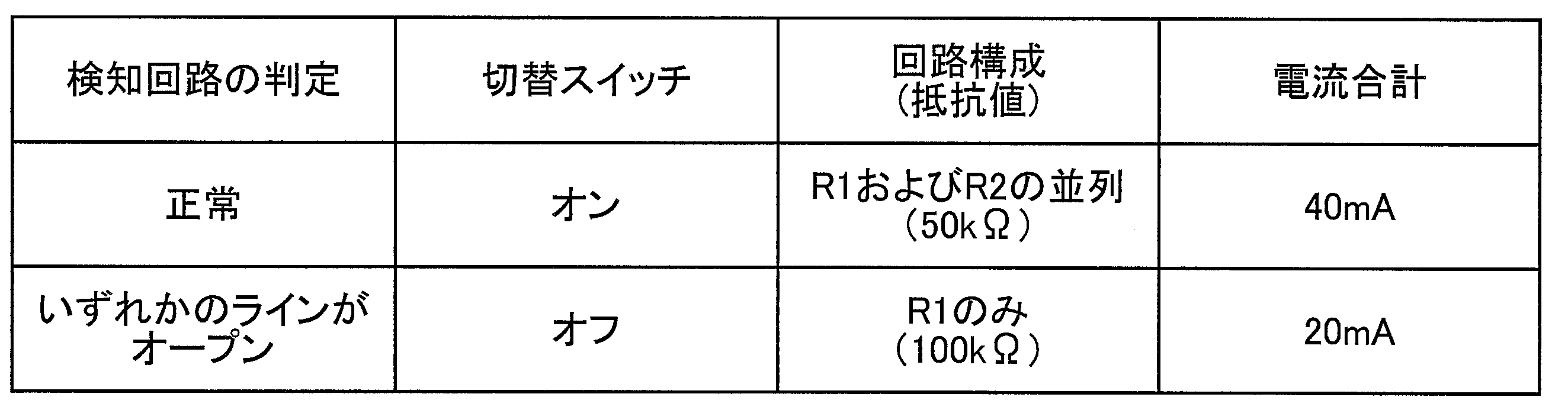
表5は、設定値提供部22aが表4に示す抵抗値を提供する場合の、具体的な切替スイッチSWならびに抵抗R1および抵抗R2の回路構成例を示す表である。
表5に示すように、発光ライン(発光ラインL1、発光ラインL2)が非オープンでありオープン検知回路(オープン検知回路SC1、オープン検知回路SC2)の判定が正常である場合には、切替スイッチSWをオンにする。これにより、抵抗R1および抵抗R2が並列に接続される回路構成となり、汎用LED駆動IC101の抵抗入力端子ITrに、抵抗値50kΩが入力(提供)される。また、いずれかの発光ラインがオープンである場合には、切替スイッチSWをオフにする。これにより、抵抗R1のみが汎用LED駆動IC101の抵抗入力端子に接続され、抵抗値100kΩが入力される。
なお、上述の抵抗値は、この構成に限定されるわけではなく、汎用LED駆動IC101の仕様およびオープン検知回路(オープン検知回路SC1、オープン検知回路SC2)の数に基づいて、各抵抗の抵抗値、抵抗の数、切替スイッチの数、および回路構成を変更しても良い。
また、設定値提供部22aは、抵抗R1、抵抗R2、および切替スイッチSWのようなハードゥエアを利用する構成ではなく、ソフトウェアを利用する構成としても良い。以下では、ソフトウェアを利用する設定値提供部22aの変形例である設定値提供部22b(設定値提供手段)について、詳細に説明する。
(設定値提供部22b)
図4は、図3に示すLED駆動回路2が備えている設定値提供部22aの変形例である設定値提供部22bの構成を示す図である。図4に示すように、設定値提供部22bは、変換部221(変換手段)と、メモリ222と、通信部223と、入力部224とを備えている。
図4は、図3に示すLED駆動回路2が備えている設定値提供部22aの変形例である設定値提供部22bの構成を示す図である。図4に示すように、設定値提供部22bは、変換部221(変換手段)と、メモリ222と、通信部223と、入力部224とを備えている。
また、メモリ222は、オープン検知回路SC1およびオープン検知回路SC2により検知されたオープン状態から、抵抗入力端子ITrを介して汎用LED駆動IC101へ提供する上記設定値への変換テーブルDを記憶している。
また、変換部221は、変換テーブルDに基づいて、オープン検知回路SC1およびオープン検知回路SC2により検知されたオープン状態を上記設定値に変換する。
ここで、変換テーブルDは、上記オープン検知回路(オープン検知回路SC1、オープン検知回路SC2)により検知されたオープン状態と上記設定値との対応が記載されているテーブルである。
具体的には、変換テーブルDには、表5に示す項目のうち、「検知回路の判定」および「回路構成(抵抗値)」の項目の内容が記載されている。
例えば、オープン検知回路のオープン状態「正常(すべてのオープン状態が非オープン)」と、設定値としての抵抗値「50kΩ」との対応が記載されており、変換部221は、この記載を読み込むことにより、当該オープン状態を当該設定値に変換する。
また、オープン検知回路のオープン状態「いずれかのライン(発光ラインL1、発光ラインL2)がオープン」と、設定値としての抵抗値「100kΩ」との対応が記載されており、変換部221は、この記載を読み込むことにより、当該オープン状態を当該設定値に変換する。
換言すると、変換部221は、変換テーブルDを参照し、オープン検知回路(オープン検知回路SC1、オープン検知回路SC2)により検知されたオープン状態を上記設定値に変換している。
ここで、上述のような変換テーブルDを利用した変換では、演算を介さずにオープン状態から設定値への変換が完了する。
上記構成によれば、変換部221は、オープン検知回路SC1およびオープン検知回路SC2により検知された発光ラインL1および発光ラインL2のオープン状態を、上述のように、変換テーブルDによって設定値に変換する。これにより、設定値提供部22bは、オープン検知回路SC1およびオープン検知回路SC2により検知された発光ラインL1および発光ラインL2のオープン状態に基づいた設定値を、汎用LED駆動IC101に提供することができる。
また、変換部221は、変換テーブルDを利用して演算を介さず変換を行うため、設定値提供部22bは、高速に設定値を提供できる。
すなわち、高速に発光ライン(発光ラインL1、発光ラインL2)を保護可能なLED駆動回路を提供することができる。
ここで、仮に、設定値提供部22bをハードウェア(例えば、抵抗および切替スイッチなど)によって構成しており、汎用LED駆動IC101の仕様が変更された場合には、仕様変更に応じてハードウェアを構成する部品の交換といった作業が必要となる可能性がある。
しかしながら、上述の設定値提供部22bは、例えば通信部223による通信や、入力部224による直接入力によって変換テーブルDを更新するといったより簡単な作業により、仕様変更に対応することができる。
すなわち、取扱いが容易なLED駆動回路を提供することができる。
また、上記設定値は、抵抗値を表す値であっても良い。
ここで、汎用LED駆動IC101などの、汎用の電流制御素子では、抵抗値による電流制御端子が設けられており、抵抗値による設定値の入力(提供)を必要とする場合がある。
上記構成によれば、設定値提供部22bは、汎用LED駆動IC101が抵抗値による設定値の提供を必要とする場合においても、適切に設定値を提供することができる。
すなわち、汎用の電流制御素子を利用可能なLED駆動回路を提供することができる。
(LED駆動回路2の構成のまとめ)
以上のように、LED駆動回路2は、複数の発光ライン(発光ラインL1、発光ラインL2)が互いに並列に接続されているLED駆動回路であって、LED駆動回路2に流れる電流の値の総和(電流Iallの値)を可変の目標値に制御する汎用LED駆動IC101と、汎用LED駆動IC101に設定値を提供する設定値提供部(設定値提供部22a、設定値提供部22b)とを備えており、各発光ラインは、発光部(発光部ES1、発光部ES2)と、当該発光部と直列に接続されており、当該発光ラインのオープン状態を検知するオープン検知回路(オープン検知回路SC1、オープン検知回路SC2)とを備えており、上記設定値提供部は、上記オープン検知回路により検知された発光ラインL1および発光ラインL2のオープン状態の組み合わせ毎に対応する上記設定値を生成し、汎用LED駆動IC101は、当該生成された設定値毎に、上記目標値を生成し、当該生成された目標値は、当該生成より以前の値から、オープンであると検知された発光ラインが非オープンである場合に当該発光ラインに流れる電流の値の総和を減算した値である。
以上のように、LED駆動回路2は、複数の発光ライン(発光ラインL1、発光ラインL2)が互いに並列に接続されているLED駆動回路であって、LED駆動回路2に流れる電流の値の総和(電流Iallの値)を可変の目標値に制御する汎用LED駆動IC101と、汎用LED駆動IC101に設定値を提供する設定値提供部(設定値提供部22a、設定値提供部22b)とを備えており、各発光ラインは、発光部(発光部ES1、発光部ES2)と、当該発光部と直列に接続されており、当該発光ラインのオープン状態を検知するオープン検知回路(オープン検知回路SC1、オープン検知回路SC2)とを備えており、上記設定値提供部は、上記オープン検知回路により検知された発光ラインL1および発光ラインL2のオープン状態の組み合わせ毎に対応する上記設定値を生成し、汎用LED駆動IC101は、当該生成された設定値毎に、上記目標値を生成し、当該生成された目標値は、当該生成より以前の値から、オープンであると検知された発光ラインが非オープンである場合に当該発光ラインに流れる電流の値の総和を減算した値である。
また、LED駆動回路2においても、図2に示すように、各オープン検知回路は、発光ライン(発光ラインL1、発光ラインL2)に直列に接続されている抵抗Rを備えており、抵抗Rにおける電圧降下が無い場合には、当該オープン検知回路を備えている上記発光ライン(発光ラインL1、発光ラインL2)がオープンであると、当該電圧降下が有る場合には、当該発光ラインが非オープンであると検知しても良い。
なお、図3では、オープン検知回路SC1およびオープン検知回路SC2は、発光部ES1および発光部ES2のカソード側に接続されているが、この構成に限定されるわけではなく、アノード側に接続されていても良い。
上記構成によれば、抵抗Rからなる簡単な構成のオープン検知回路(オープン検知回路SC1、オープン検知回路SC2)により、発光ライン(発光ラインL1、発光ラインL2)のオープン状態を検知することができる。
さらに、LED駆動回路2では、図4に示す構成の設定値提供部22bと、図2に示す構成のオープン検知回路(オープン検知回路SC1、オープン検知回路SC2)とを同時に備えていても良い。
<LED駆動回路2の動作>
上記構成よれば、発光ライン(発光ラインL1、発光ラインL2)がオープンである場合には、当該発光ラインに電流が流れない。そして、当該発光ラインに備えられているオープン検知回路(オープン検知回路SC1、オープン検知回路SC2)は、当該発光ラインがオープンであることを検知する。設定値提供部(設定値提供部22a、設定値提供部22b)は、当該検知された発光ラインのオープン状態の組み合わせ毎に対応する、設定値を生成する。汎用LED駆動IC101は、当該生成された設定値に基づいて、目標値を生成する。
上記構成よれば、発光ライン(発光ラインL1、発光ラインL2)がオープンである場合には、当該発光ラインに電流が流れない。そして、当該発光ラインに備えられているオープン検知回路(オープン検知回路SC1、オープン検知回路SC2)は、当該発光ラインがオープンであることを検知する。設定値提供部(設定値提供部22a、設定値提供部22b)は、当該検知された発光ラインのオープン状態の組み合わせ毎に対応する、設定値を生成する。汎用LED駆動IC101は、当該生成された設定値に基づいて、目標値を生成する。
ここで、当該生成された目標値は、当該生成より以前の値から、オープンであると検知された発光ラインが非オープンである場合に当該発光ラインに流れる電流の値の総和を減算した値である。
よって、目標値は、LED駆動回路2に流れる電流の値の総和(電流Iallの値)の低下に応じて小さくなっている。
仮に、複数の発光ライン(発光ラインL1、発光ラインL2)のいずれかの発光ラインがオープンである場合には、LED駆動回路2に流れる電流の値の総和(電流Iallの値)が低下する。そして、当該総和が目標値より小さくなる場合には、汎用LED駆動IC101により電流制御が行われ、当該総和が元の値に戻される。ここで、オープンである発光ラインは電流を流さないので、非オープンである残りの発光ラインに過大な電流が集中し、当該発光ラインが破壊される可能性がある。
しかしながら、目標値は、当該総和の低下に応じて小さくなっているため、当該破壊から発光ライン(発光ラインL1、発光ラインL2)を保護することができる。
また、当該目標値の変更において、発光部(発光部ES1、発光部ES2)における発光以外には、何らの電力も消費されない。
すなわち、流れる電流の値が制御されているLED駆動回路において、発光ラインを保護可能かつ低消費電力なLED駆動回路を提供することができる。
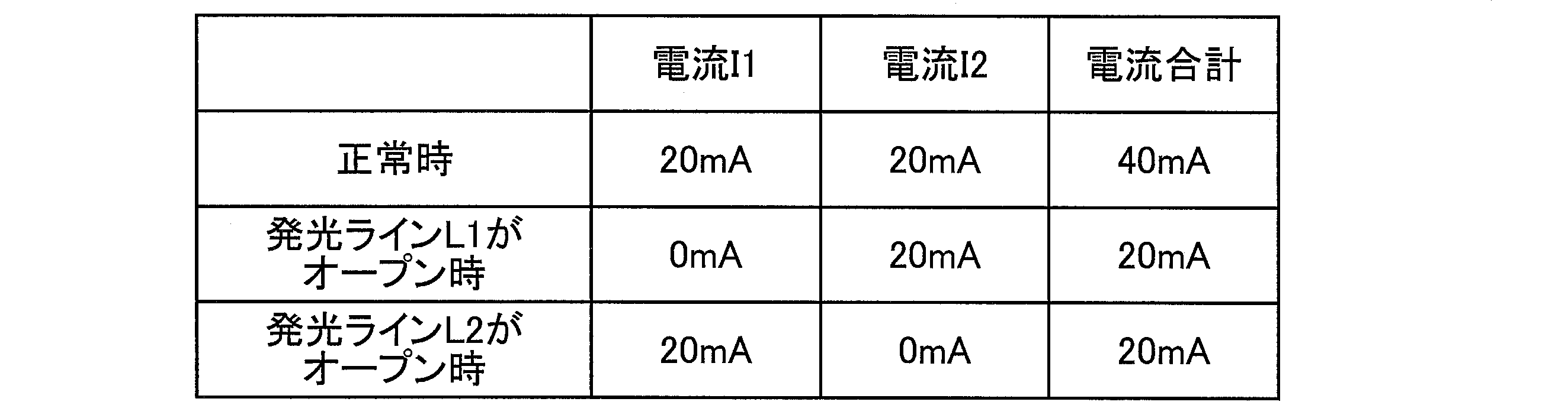
表6は、LED駆動回路2の発光ラインL1に流れる電流I1の値と、発光ラインL2に流れる電流I2の値と、電流I1および電流I2の値の合計(電流合計)を示す表である。表6に示すように、発光ラインL1および発光ラインL2が非オープンである正常時には、電流I1の値は20mAとなり、電流I2の値は20mAとなる。よって、電流合計は40mAである。
次に、発光ラインL1がオープンである場合には、発光ラインL1に電流が流れないため、電流I1の値は0mAになる。なお、発光ラインL2は非オープンであるので、電流I2の値は20mAとなる。よって、電流合計は20mAである。ここで、LED駆動回路2に流れる電流Iallの値は、電流I1の値および電流I2の値の合計となっている。つまり、LED駆動回路2に流れる電流Iallが、一定値20mAになるように制御されている。
次に、発光ラインL2がオープンである場合には、発光ラインL2に電流が流れないため、電流I2の値は0mAになる。なお、発光ラインL1は非オープンであるので、電流I1の値は20mAとなる。つまり、LED駆動回路2に流れる電流Iallが、一定値20mAになるように制御されている。
以上のように、LED駆動回路2では、非オープンである発光ラインに流れる電流が一定値(20mA)になるように制御されている。
<LED駆動回路2の効果>
本実施形態によれば、流れる電流の値が制御されている回路において、発光ラインを保護可能かつ低消費電力なLED駆動回路を提供することができる。
本実施形態によれば、流れる電流の値が制御されている回路において、発光ラインを保護可能かつ低消費電力なLED駆動回路を提供することができる。
また、本実施形態によれば、低コストなLED駆動回路を提供することができる。
また、本実施形態によれば、高速に発光ラインを保護可能なLED駆動回路を提供することができる。
また、本実施形態によれば、取扱いが容易なLED駆動回路を提供することができる。
また、本実施形態によれば、汎用のLED駆動ICを利用可能なLED駆動回路を提供することができる。
以下では、LED駆動回路の電位差を制御する電圧制御素子を備えているLED駆動回路に関する実施形態について説明する。
〔実施形態3〕
本発明の他の実施形態について、図5に基づいて説明すれば、以下のとおりである。なお、説明の便宜上、上記実施形態にて説明した図面と同一の機能を有する部材については、同一の符号を付記し、その説明を省略する。
本発明の他の実施形態について、図5に基づいて説明すれば、以下のとおりである。なお、説明の便宜上、上記実施形態にて説明した図面と同一の機能を有する部材については、同一の符号を付記し、その説明を省略する。
<LED駆動回路3の構成>
図5は、本発明の他の実施形態に係るLED駆動回路(回路)3の構成を示す図である。図5に示すように、LED駆動回路3は、LED駆動回路1と同様に、発光モジュール10を備えている。
図5は、本発明の他の実施形態に係るLED駆動回路(回路)3の構成を示す図である。図5に示すように、LED駆動回路3は、LED駆動回路1と同様に、発光モジュール10を備えている。
しかしながら、LED駆動回路3は、汎用LED駆動IC101ではなく汎用LED駆動IC(電圧制御素子)101aを備えており、汎用LED駆動IC101aが調光(電圧調光)端子ITvを備えている点が、LED駆動回路1とは異なっている。
また、汎用LED駆動IC101aは、LED駆動回路3の電位差Vを制御する電圧制御素子である。
また、汎用LED駆動IC101aは、調光端子ITvおよび制御出力端子OTを備えており、各端子において他の構成要素と接続されている。
また、定電流化ラインCI1および定電流化ラインCI2は、それぞれに対応している上記発光ライン(発光ラインL1および発光ラインL2)に備えられている上記発光部(発光部ES1、発光部ES2)の抵抗値と概ね同一の抵抗値を有している抵抗(抵抗SR1、抵抗SR2)を備えている。
つまり、LED駆動回路3は、複数の発光ライン(発光ラインL1、発光ラインL1)が互いに並列に接続されており、電位差Vを制御する電圧制御素子(汎用LED駆動IC101a)を備えているLED駆動回路であって、各発光ラインに対応して並列に接続されている定電流化ライン(定電流化ラインCI1、定電流化ラインCI2)とを備えており、各発光ラインは、発光部(発光部ES1、発光部ES2)と、当該発光部と直列に接続されており、当該発光ラインのオープン状態を検知するオープン検知回路(オープン検知回路SC1、オープン検知回路SC2)とを備えており、各定電流化ラインは、当該定電流化ラインそれぞれに対応している上記発光ラインに備えられている上記発光部の抵抗値と概ね同一の抵抗値を有している抵抗(抵抗SR1、抵抗SR2)と、当該抵抗と直列に接続されており、当該定電流化ラインのオープン状態を切り替える切替スイッチ(切替スイッチSW1、切替スイッチSW2)とを備えており、上記切替スイッチは、当該切替スイッチを備えている上記定電流化ラインと対応する上記発光ラインに備えられている上記オープン検知回路により検知されたオープン状態が、オープンである場合には当該定電流化ラインを非オープンに切り替え、非オープンである場合には当該定電流化ラインをオープンに切り替える。
また、LED駆動回路3においても、図2に示すように、各オープン検知回路は、発光ライン(発光ラインL1、発光ラインL2)に直列に接続されている抵抗Rを備えており、抵抗Rにおける電圧降下が無い場合には、当該オープン検知回路を備えている上記発光ライン(発光ラインL1、発光ラインL2)がオープンであると、当該電圧降下が有る場合には、当該発光ラインが非オープンであると検知しても良い。
なお、図5では、オープン検知回路SC1およびオープン検知回路SC2は、発光部ES1および発光部ES2のカソード側に接続されているが、この構成に限定されるわけではなく、アノード側に接続されていても良い。
上記構成によれば、抵抗Rからなる簡単な構成のオープン検知回路(オープン検知回路SC1、オープン検知回路SC2)により、発光ライン(発光ラインL1、発光ラインL2)のオープン状態を検知することができる。
<LED駆動回路3の動作>
上記構成によれば、発光ライン(発光ラインL1、発光ラインL2)がオープンである場合には、当該発光ラインに電流が流れない。そして、当該発光ラインに備えられているオープン検知回路(オープン検知回路SC1、オープン検知回路SC2)は、当該発光ラインがオープンであることを検知し、当該発光ラインに対応している定電流化ライン(定電流化ラインCI1、定電流化ラインCI2)に備えられている切替スイッチ(切替スイッチSW1、切替スイッチSW2)により、当該定電流化ラインは、非オープンに切り替えられる。これにより、当該定電流化ラインに備えられている抵抗(抵抗SR1、抵抗SR2)に電位差が生じ、当該定電流化ラインに電流が流れる。
上記構成によれば、発光ライン(発光ラインL1、発光ラインL2)がオープンである場合には、当該発光ラインに電流が流れない。そして、当該発光ラインに備えられているオープン検知回路(オープン検知回路SC1、オープン検知回路SC2)は、当該発光ラインがオープンであることを検知し、当該発光ラインに対応している定電流化ライン(定電流化ラインCI1、定電流化ラインCI2)に備えられている切替スイッチ(切替スイッチSW1、切替スイッチSW2)により、当該定電流化ラインは、非オープンに切り替えられる。これにより、当該定電流化ラインに備えられている抵抗(抵抗SR1、抵抗SR2)に電位差が生じ、当該定電流化ラインに電流が流れる。
ここで、当該抵抗は、当該定電流化ラインと対応している発光ライン(発光ラインL1、発光ラインL2)に備えられている発光部(発光部ES1、発光部ES2)の抵抗値と概ね同一の抵抗値を有している。これにより、当該定電流化ラインに流れる電流は、当該定電流化ラインと対応している発光ライン(発光ラインL1、発光ラインL2)が非オープンである場合に当該発光ラインに流れる電流の値と概ね同一の値を有している。
よって、発光ライン(発光ラインL1、発光ラインL2)がオープンであっても、当該発光ラインが非オープンである場合と概ね同一の値を有している電流が、定電流化ライン(定電流化ラインCI1、定電流化ラインCI2)から回路に供給される。
仮に、LED駆動回路3が定電流化ライン(定電流化ラインCI1、定電流化ラインCI2)を備えていなければ、複数の発光ライン(発光ラインL1、発光ラインL2)のいずれかの発光ラインがオープンである場合には、LED駆動回路3に流れる電流の値の総和(電流Iallの値)が低下する。ここで、汎用LED駆動IC101aは、電流制御素子とは異なり、電圧制御素子であるので、LED駆動回路3に流れる電流の値の監視などを行っておらず、当該電流の値の変化により正常な動作が阻害される可能性がある。また、これにより、発光ライン(発光ラインL1、発光ラインL2)が破壊される可能性がある。
しかしながら、LED駆動回路3は、上述の定電流化ライン(定電流化ラインCI1、定電流化ラインCI2)を備えているため、電流制御がなされていなくてもLED駆動回路3に流れる電流の値の総和(電流Iallの値)を概ね一定値に維持することができ、当該破壊から発光ライン(発光ラインL1、発光ラインL2)を保護することができる。
また、発光ライン(発光ラインL1、発光ラインL2)が非オープン(正常)である場合には、対応する定電流化ラインがオープンであるため、発光部(発光部ES1、発光部ES2)における発光以外には、何らの電力も消費されない。
<LED駆動回路3の効果>
本実施形態によれば、電位差が制御されているLED駆動回路において、発光ラインを保護可能かつ低消費電力なLED駆動回路を提供することができる。
本実施形態によれば、電位差が制御されているLED駆動回路において、発光ラインを保護可能かつ低消費電力なLED駆動回路を提供することができる。
また、低コストなLED駆動回路を提供することができる。
〔まとめ〕
本発明の一態様に係る回路(LED駆動回路1)は、複数の発光ラインが互いに並列に接続されており、流れる電流の値の総和を一定値に制御する電流制御素子(汎用LED駆動IC101)を備えている回路であって、各発光ラインに対応して並列に接続されている定電流化ラインを備えており、各発光ラインは、発光部と、当該発光部と直列に接続されており、当該発光ラインのオープン状態を検知する検知部(オープン検知回路SC1、オープン検知回路SC2)とを備えており、各定電流化ラインは、当該定電流化ラインそれぞれに対応している上記発光ラインが非オープンである場合に当該発光ラインに流れる電流の値と概ね同一の値を有している電流を生起する定電流源と、当該定電流源と直列に接続されており、当該定電流化ラインのオープン状態を切り替える切替スイッチとを備えており、上記切替スイッチは、当該切替スイッチを備えている上記定電流化ラインと対応する上記発光ラインに備えられている上記検知部により検知されたオープン状態が、オープンである場合には当該定電流化ラインを非オープンに切り替え、非オープンである場合には当該定電流化ラインをオープンに切り替える。
本発明の一態様に係る回路(LED駆動回路1)は、複数の発光ラインが互いに並列に接続されており、流れる電流の値の総和を一定値に制御する電流制御素子(汎用LED駆動IC101)を備えている回路であって、各発光ラインに対応して並列に接続されている定電流化ラインを備えており、各発光ラインは、発光部と、当該発光部と直列に接続されており、当該発光ラインのオープン状態を検知する検知部(オープン検知回路SC1、オープン検知回路SC2)とを備えており、各定電流化ラインは、当該定電流化ラインそれぞれに対応している上記発光ラインが非オープンである場合に当該発光ラインに流れる電流の値と概ね同一の値を有している電流を生起する定電流源と、当該定電流源と直列に接続されており、当該定電流化ラインのオープン状態を切り替える切替スイッチとを備えており、上記切替スイッチは、当該切替スイッチを備えている上記定電流化ラインと対応する上記発光ラインに備えられている上記検知部により検知されたオープン状態が、オープンである場合には当該定電流化ラインを非オープンに切り替え、非オープンである場合には当該定電流化ラインをオープンに切り替える。
ここで、オープン状態とは、発光ラインまたは定電流化ラインなどの電気回路における、電気的な接続状態を意味している。
また、オープン状態が「オープン」であるとは、上記電気回路の一部が電気的に接続されておらず、当該電気回路に電流が流れ得ない状態であることを意味する。例えば、発光ラインは、発光部の破損などによる異常が発生している場合には、オープン状態がオープンになり得る。また、例えば、定電流化ラインは、切替スイッチにより電気回路の一部が開かれている場合には、オープン状態がオープンになり得る。
また、オープン状態が「非オープン」であるとは、上記電気回路に電流が流れ得る状態であることを意味する。例えば、発光ラインは、発光部が正常に機能している場合には、オープン状態が非オープンになり得る。また、例えば、定電流化ラインは、切替スイッチにより電気回路の一部が閉じられている場合には、オープン状態が非オープンになり得る。
上記構成によれば、発光ラインがオープンである場合には、当該発光ラインに電流が流れない。そして、当該発光ラインに備えられている検知部は、当該発光ラインがオープンであることを検知し、当該発光ラインに対応している定電流化ラインに備えられている切替スイッチにより、当該定電流化ラインは、非オープンに切り替えられる。これにより、当該定電流化ラインに備えられている定電流源から電流が供給され、当該定電流化ラインに電流が流れる。
ここで、当該定電流化ラインに流れる電流は、当該定電流化ラインと対応している発光ラインが非オープンである場合に当該発光ラインに流れる電流の値と概ね同一の値を有している。
なお、「概ね同一の値」とは、必ずしも同一の値である必要はないということを意味している。さらには、当該値が、何らかの理由により変動しても良いということである。
例えば、定電流源が生起する電流の値は、回路を構成する構成要素の経年劣化や、回路が置かれる環境(ここで、環境とは、例えば温度や湿度などであっても良い)により変動し得る。しかしながら、当該電流の値は、当該発光ラインが備えている上記発光部の電流の絶対最大定格値を越えない、または、当該発光ラインが破壊に至らない範囲であれば、その変動を許容でき、概ね同一の値であると言える。
よって、発光ラインがオープンであっても、当該発光ラインが非オープンである場合と概ね同一の値を有している電流が、定電流化ラインから回路に供給される。
仮に、回路が定電流化ラインを備えていなければ、複数の発光ラインのいずれかの発光ラインがオープンである場合には、回路に流れる電流の値の総和が低下するが、電流制御素子により電流制御が行われ、当該総和が元の値に戻される。ここで、オープンである発光ラインは電流を流さないので、非オープンである残りの発光ラインに過大な電流が集中し、当該発光ラインが破壊される可能性がある。
しかしながら、回路は、上述の定電流化ラインを備えているため、当該破壊から発光ラインを保護することができる。
また、発光ラインが非オープン(正常)である場合には、対応する定電流化ラインがオープンであるため、発光部における発光以外には、何らの電力も消費されない。
すなわち、流れる電流の値が制御されている回路において、発光ラインを保護可能かつ低消費電力な回路を提供することができる。
また、本発明の一態様に係る回路(LED駆動回路2)は、複数の発光ラインが互いに並列に接続されている回路であって、上記回路に流れる電流の値の総和を可変の目標値に制御する電流制御素子と、上記電流制御素子に設定値を提供する設定値提供手段(設定値提供部22a、設定値提供部22b)とを備えており、各発光ラインは、発光部と、当該発光部と直列に接続されており、当該発光ラインのオープン状態を検知する検知部とを備えており、上記設定値提供手段は、上記検知部により検知された上記複数の発光ラインのオープン状態の組み合わせ毎に対応する上記設定値を生成し、上記電流制御素子は、当該生成された設定値毎に、上記目標値を生成し、当該生成された目標値は、当該生成より以前の値から、オープンであると検知された発光ラインが非オープンである場合に当該発光ラインに流れる電流の値の総和を減算した値である。
上記構成によれば、発光ラインがオープンである場合には、当該発光ラインに電流が流れない。そして、当該発光ラインに備えられている検知部は、当該発光ラインがオープンであることを検知する。設定値提供手段は、当該検知された発光ラインのオープン状態に基づいて、設定値を変更する。電流制御素子は、当該変更された設定値に基づいて、目標値を変更する。
ここで、当該変更された目標値は、当該変更より以前の値から、オープンであると検知された発光ラインが非オープンである場合に当該発光ラインに流れる電流の値の総和を減算した値である。
よって、目標値は、回路に流れる電流の値の総和の低下に応じて小さくなっている。
仮に、複数の発光ラインのいずれかの発光ラインがオープンである場合には、回路に流れる電流の値の総和が低下する。そして、当該総和が目標値より小さくなる場合には、電流制御素子により電流制御が行われ、当該総和が元の値に戻される。ここで、オープンである発光ラインは電流を流さないので、非オープンである残りの発光ラインに過大な電流が集中し、当該発光ラインが破壊される可能性がある。
しかしながら、目標値は、当該総和の低下に応じて小さくなっているため、当該破壊から発光ラインを保護することができる。
また、当該目標値の変更において、発光部における発光以外には、何らの電力も消費されない。
すなわち、流れる電流の値が制御されている回路において、発光ラインを保護可能かつ低消費電力な回路を提供することができる。
また、本発明の一態様に係る回路では、上記設定値提供手段は、複数の抵抗と、上記複数の抵抗を切り替えて組み合わせる切替スイッチとを備えており、上記切替スイッチは、上記検知部により検知された上記複数の発光ラインのオープン状態の組み合わせ毎に対応して切り替えられ、上記設定値は、上記設定値提供手段の抵抗値であっても良い。
上記構成によれば、切替スイッチにより複数の抵抗を組み合わせた簡単な構成の設定値提供手段により、検知部で検知されたオープン状態に基づいた所望の抵抗値を、設定値として電流制御素子に提供することができる。これにより、設定値提供手段を低コスト化することができる。
すなわち、低コストな回路を提供することができる。
また、本発明の一態様に係る回路では、上記設定値提供手段は、上記検知部により検知されたオープン状態と上記設定値との対応を記載している変換テーブルを記憶しているメモリと、当該変換テーブルを参照し、上記検知部により検知されたオープン状態を上記設定値に変換する変換手段(変換部221)とを備えていても良い。
上記構成によれば、変換手段は、検知部により検知された発光ラインのオープン状態を、変換テーブルによって設定値に変換する。これにより、設定値提供手段は、検知部により検知された発光ラインのオープン状態に基づいた設定値を、電流制御素子に提供することができる。
また、変換手段は、変換テーブルを利用して演算を介さず変換を行うため、設定値提供手段は、高速に設定値を提供できる。
すなわち、高速に発光ラインを保護可能な回路を提供することができる。
ここで、仮に、設定値提供手段をハードウェア(例えば、抵抗および切替スイッチなど)によって構成しており、電流制御素子の仕様が変更された場合には、仕様変更に応じてハードウェアを構成する部品の交換といった作業が必要となる可能性がある。
しかしながら、上述の設定値提供手段は、例えば通信や直接入力による変換テーブルの更新といったより簡単な作業により、仕様変更に対応することができる。
すなわち、取扱いが容易な回路を提供することができる。
また、本発明の一態様に係る回路では、上記設定値は、抵抗値を表す値であっても良い。
ここで、汎用の電流制御素子(例えば、LED駆動ICなど)では、抵抗値による電流制御端子が設けられており、抵抗値による設定値の入力(提供)を必要とする場合がある。
上記構成によれば、設定値提供手段は、電流制御素子が抵抗値による設定値の提供を必要とする場合においても、適切に設定値を提供することができる。
すなわち、汎用の電流制御素子を利用可能な回路を提供することができる。
また、本発明の一態様に係る回路(LED駆動回路3)は、複数の発光ラインが互いに並列に接続されており、電位差を制御する電圧制御素子(汎用LED駆動IC101a)を備えている回路であって、各発光ラインに対応して並列に接続されている定電流化ラインを備えており、各発光ラインは、発光部と、当該発光部と直列に接続されており、当該発光ラインのオープン状態を検知する検知部とを備えており、各定電流化ラインは、当該定電流化ラインそれぞれに対応している上記発光ラインに備えられている上記発光部の抵抗値と概ね同一の抵抗値を有している抵抗と、当該抵抗と直列に接続されており、当該定電流化ラインのオープン状態を切り替える切替スイッチとを備えており、上記切替スイッチは、当該切替スイッチを備えている上記定電流化ラインと対応する上記発光ラインに備えられている上記検知部により検知されたオープン状態が、オープンである場合には当該定電流化ラインを非オープンに切り替え、非オープンである場合には当該定電流化ラインをオープンに切り替える。
上記構成によれば、発光ラインがオープンである場合には、当該発光ラインに電流が流れない。そして、当該発光ラインに備えられている検知部は、当該発光ラインがオープンであることを検知し、当該発光ラインに対応している定電流化ラインに備えられている切替スイッチにより、当該定電流化ラインは、非オープンに切り替えられる。これにより、当該定電流化ラインに備えられている抵抗に電位差が生じ、当該定電流化ラインに電流が流れる。
ここで、当該抵抗は、当該定電流化ラインと対応している発光ラインに備えられている発光部の抵抗値と概ね同一の抵抗値を有している。これにより、当該定電流化ラインに流れる電流は、当該定電流化ラインと対応している発光ラインが非オープンである場合に当該発光ラインに流れる電流の値と概ね同一の値を有している。
なお、「概ね同一の抵抗値」とは、必ずしも同一の抵抗値である必要はないということを意味している。さらには、当該抵抗値が、何らかの理由により変動しても良いということである。
例えば、抵抗に電位差が生じ当該抵抗および当該定電流化ラインに流れる電流の値は、回路を構成する構成要素または当該抵抗自体の経年劣化や、回路が置かれる環境(ここで、環境とは、例えば温度や湿度などであっても良い)により変動し得る。しかしながら、当該電流の値は、当該発光ラインが備えている上記発光部の電流の絶対最大定格値を越えない、または、当該発光ラインが破壊に至らない範囲であれば、その変動を許容でき、概ね同一の値であると言える。そして、当該抵抗の抵抗値も、その変動を許容することができる。
よって、発光ラインがオープンであっても、当該発光ラインが非オープンである場合と概ね同一の値を有している電流が、定電流化ラインから回路に供給される。
仮に、回路が定電流化ラインを備えていなければ、複数の発光ラインのいずれかの発光ラインがオープンである場合には、回路に流れる電流の値の総和が低下する。ここで、電圧制御素子は、電流制御素子とは異なり、回路に流れる電流の値の監視などを行っておらず、当該電流の値の変化により正常な動作が阻害される可能性がある。また、これにより、発光ラインが破壊される可能性がある。
しかしながら、回路は、上述の定電流化ラインを備えているため、電流制御がなされていなくても回路に流れる電流の値の総和を概ね一定値に維持することができ、当該破壊から発光ラインを保護することができる。
また、発光ラインが非オープン(正常)である場合には、対応する定電流化ラインがオープンであるため、発光部における発光以外には、何らの電力も消費されない。
すなわち、電位差が制御されている回路において、発光ラインを保護可能かつ低消費電力な回路を提供することができる。
また、本発明の一態様に係る回路では、上記検知部は、上記発光ラインに直列に接続されている抵抗を備えており、当該抵抗における電圧降下が無い場合には、当該検知部を備えている上記発光ラインがオープンであると、当該電圧降下が有る場合には、当該発光ラインが非オープンであると検知しても良い。
上記構成によれば、抵抗からなる簡単な構成の検知部により、発光ラインのオープン状態を検知することができる。
すなわち、低コストな回路を提供することができる。
また、本発明の一態様に係る回路では、制御プログラムにより、コンピュータを、上記変換手段として機能させることができる。さらに、当該制御プログラムを、コンピュータ読み取り可能な記録媒体に記録させることにより、汎用なコンピュータ上で上記制御プログラムを実行させることができる。
〔付記事項〕
本発明は上述した各実施形態に限定されるものではなく、請求項に示した範囲で種々の変更が可能であり、異なる実施形態にそれぞれ開示された技術的手段を適宜組み合わせて得られる実施形態についても本発明の技術的範囲に含まれる。
本発明は上述した各実施形態に限定されるものではなく、請求項に示した範囲で種々の変更が可能であり、異なる実施形態にそれぞれ開示された技術的手段を適宜組み合わせて得られる実施形態についても本発明の技術的範囲に含まれる。
〔ソフトウェアによる実現例〕
最後に、設定値提供部22bが備えている変換部221は、集積回路(ICチップ)上に形成された論理回路によってハードウェア的に実現してもよいし、CPU(Central Processing Unit)を用いてソフトウェア的に実現してもよい。
最後に、設定値提供部22bが備えている変換部221は、集積回路(ICチップ)上に形成された論理回路によってハードウェア的に実現してもよいし、CPU(Central Processing Unit)を用いてソフトウェア的に実現してもよい。
後者の場合、設定値提供部22bは、各機能を実現するプログラムの命令を実行するCPU、上記プログラムを格納したROM(Read Only Memory)、上記プログラムを展開するRAM(Random Access Memory)、上記プログラムおよび各種データを格納するメモリ等の記憶装置(記録媒体)などを備えている。そして、本発明の目的は、上述した機能を実現するソフトウェアである設定値提供部22bの制御プログラムのプログラムコード(実行形式プログラム、中間コードプログラム、ソースプログラム)をコンピュータで読み取り可能に記録した記録媒体を、上記設定値提供部22bに供給し、そのコンピュータ(またはCPUやMPU)が記録媒体に記録されているプログラムコードを読み出し実行することによっても、達成可能である。
上記記録媒体としては、一時的でない有形の媒体(non-transitory tangible medium)、例えば、磁気テープやカセットテープ等のテープ類、フロッピー(登録商標)ディスク/ハードディスク等の磁気ディスクやCD-ROM/MO/MD/DVD/CD-R等の光ディスクを含むディスク類、ICカード(メモリカードを含む)/光カード等のカード類、マスクROM/EPROM/EEPROM(登録商標)/フラッシュROM等の半導体メモリ類、あるいはPLD(Programmable logic device)やFPGA(Field Programmable Gate Array)等の論理回路類などを用いることができる。
また、設定値提供部22bを通信ネットワークと接続可能に構成し、上記プログラムコードを通信ネットワークを介して供給してもよい。この通信ネットワークは、プログラムコードを伝送可能であればよく、特に限定されない。例えば、インターネット、イントラネット、エキストラネット、LAN、ISDN、VAN、CATV通信網、仮想専用網(Virtual Private Network)、電話回線網、移動体通信網、衛星通信網等が利用可能である。また、この通信ネットワークを構成する伝送媒体も、プログラムコードを伝送可能な媒体であればよく、特定の構成または種類のものに限定されない。例えば、IEEE1394、USB、電力線搬送、ケーブルTV回線、電話線、ADSL(Asymmetric Digital Subscriber Line)回線等の有線でも、IrDAやリモコンのような赤外線、Bluetooth(登録商標)、IEEE802.11無線、HDR(High Data Rate)、NFC(Near Field Communication)、DLNA(登録商標)(Digital Living Network Alliance)、携帯電話網、衛星回線、地上波デジタル網等の無線でも利用可能である。なお、本発明は、上記プログラムコードが電子的な伝送で具現化された、搬送波に埋め込まれたコンピュータデータ信号の形態でも実現され得る。
本発明は上述した各実施形態に限定されるものではなく、請求項に示した範囲で種々の変更が可能であり、異なる実施形態にそれぞれ開示された技術的手段を適宜組み合わせて得られる実施形態についても本発明の技術的範囲に含まれる。さらに、各実施形態にそれぞれ開示された技術的手段を組み合わせることにより、新しい技術的特徴を形成することができる。
本発明は、光源としてLEDを採用したディスプレイ装置に広く利用することができる。また、多数の発光素子を一括して駆動する発光装置全般に利用することができる。
1 LED駆動回路(回路)
2 LED駆動回路(回路)
3 LED駆動回路(回路)
10 発光モジュール
10a 発光モジュール
22a 設定値提供部(設定値提供手段)
22b 設定値提供部(設定値提供手段)
101 汎用LED駆動IC(電流制御素子)
101a 汎用LED駆動IC(電圧制御素子)
221 変換部(変換手段)
CI1 定電流化ライン
CI2 定電流化ライン
D 変換テーブル
ES1 発光部
ES2 発光部
I1 電流
I2 電流
Iall 電流
L1 発光ライン
L2 発光ライン
R 抵抗
R1 抵抗
R2 抵抗
S1 定電流源
S2 定電流源
SC1 オープン検知回路(検知部)
SC2 オープン検知回路(検知部)
SR1 抵抗
SR2 抵抗
SW 切替スイッチ
SW1 切替スイッチ
SW2 切替スイッチ
2 LED駆動回路(回路)
3 LED駆動回路(回路)
10 発光モジュール
10a 発光モジュール
22a 設定値提供部(設定値提供手段)
22b 設定値提供部(設定値提供手段)
101 汎用LED駆動IC(電流制御素子)
101a 汎用LED駆動IC(電圧制御素子)
221 変換部(変換手段)
CI1 定電流化ライン
CI2 定電流化ライン
D 変換テーブル
ES1 発光部
ES2 発光部
I1 電流
I2 電流
Iall 電流
L1 発光ライン
L2 発光ライン
R 抵抗
R1 抵抗
R2 抵抗
S1 定電流源
S2 定電流源
SC1 オープン検知回路(検知部)
SC2 オープン検知回路(検知部)
SR1 抵抗
SR2 抵抗
SW 切替スイッチ
SW1 切替スイッチ
SW2 切替スイッチ
Claims (9)
- 複数の発光ラインが互いに並列に接続されており、流れる電流の値の総和を一定値に制御する電流制御素子を備えている回路であって、
各発光ラインに対応して並列に接続されている定電流化ラインを備えており、
各発光ラインは、
発光部と、
当該発光部と直列に接続されており、当該発光ラインのオープン状態を検知する検知部とを備えており、
各定電流化ラインは、
当該定電流化ラインそれぞれに対応している上記発光ラインが非オープンである場合に当該発光ラインに流れる電流の値と概ね同一の値を有している電流を生起する定電流源と、
当該定電流源と直列に接続されており、当該定電流化ラインのオープン状態を切り替える切替スイッチとを備えており、
上記切替スイッチは、当該切替スイッチを備えている上記定電流化ラインと対応する上記発光ラインに備えられている上記検知部により検知されたオープン状態が、オープンである場合には当該定電流化ラインを非オープンに切り替え、非オープンである場合には当該定電流化ラインをオープンに切り替えることを特徴とする回路。 - 複数の発光ラインが互いに並列に接続されている回路であって、
上記回路に流れる電流の値の総和を可変の目標値に制御する電流制御素子と、
上記電流制御素子に設定値を提供する設定値提供手段とを備えており、
各発光ラインは、
発光部と、
当該発光部と直列に接続されており、当該発光ラインのオープン状態を検知する検知部とを備えており、
上記設定値提供手段は、上記検知部により検知された上記複数の発光ラインのオープン状態の組み合わせ毎に対応する上記設定値を生成し、
上記電流制御素子は、
当該生成された設定値毎に、上記目標値を生成し、
当該生成された目標値は、当該生成より以前の値から、オープンであると検知された上記発光ラインが非オープンである場合に当該発光ラインに流れる電流の値の総和を減算した値であることを特徴とする回路。 - 上記設定値提供手段は、
複数の抵抗と、
上記複数の抵抗を切り替えて組み合わせる切替スイッチとを備えており、
上記切替スイッチは、上記検知部により検知された上記複数の発光ラインのオープン状態の組み合わせ毎に対応して切り替えられ、
上記設定値は、上記設定値提供手段の抵抗値であることを特徴とする請求項2に記載の回路。 - 上記設定値提供手段は、
上記検知部により検知されたオープン状態と上記設定値との対応を記載している変換テーブルを記憶しているメモリと、
当該変換テーブルを参照し、上記検知部により検知されたオープン状態を上記設定値に変換する変換手段とを備えていることを特徴とする請求項2に記載の回路。 - 上記設定値は、抵抗値を表す値であることを特徴とする請求項4に記載の回路。
- 複数の発光ラインが互いに並列に接続されており、電位差を制御する電圧制御素子を備えている回路であって、
各発光ラインに対応して並列に接続されている定電流化ラインを備えており、
各発光ラインは、
発光部と、
当該発光部と直列に接続されており、当該発光ラインのオープン状態を検知する検知部とを備えており、
各定電流化ラインは、
当該定電流化ラインそれぞれに対応している上記発光ラインに備えられている上記発光部の抵抗値と概ね同一の抵抗値を有している抵抗と、
当該抵抗と直列に接続されており、当該定電流化ラインのオープン状態を切り替える切替スイッチとを備えており、
上記切替スイッチは、当該切替スイッチを備えている上記定電流化ラインと対応する上記発光ラインに備えられている上記検知部により検知されたオープン状態が、オープンである場合には当該定電流化ラインを非オープンに切り替え、非オープンである場合には当該定電流化ラインをオープンに切り替えることを特徴とする回路。 - 上記検知部は、
上記発光ラインに直列に接続されている抵抗を備えており、
当該抵抗における電圧降下が無い場合には、当該検知部を備えている上記発光ラインがオープンであると、当該電圧降下が有る場合には、当該発光ラインが非オープンであると検知することを特徴とする請求項1~6のいずれか1項に記載の回路。 - コンピュータを、請求項4または5に記載の回路に備えられた変換手段として機能させるための制御プログラム。
- 請求項8に記載の制御プログラムを記録したコンピュータ読み取り可能な記録媒体。
Priority Applications (1)
| Application Number | Priority Date | Filing Date | Title |
|---|---|---|---|
| US14/434,493 US9204513B2 (en) | 2012-10-22 | 2013-10-02 | Circuit, control program, and recording medium |
Applications Claiming Priority (2)
| Application Number | Priority Date | Filing Date | Title |
|---|---|---|---|
| JP2012-233088 | 2012-10-22 | ||
| JP2012233088 | 2012-10-22 |
Publications (1)
| Publication Number | Publication Date |
|---|---|
| WO2014065091A1 true WO2014065091A1 (ja) | 2014-05-01 |
Family
ID=50544471
Family Applications (1)
| Application Number | Title | Priority Date | Filing Date |
|---|---|---|---|
| PCT/JP2013/076852 Ceased WO2014065091A1 (ja) | 2012-10-22 | 2013-10-02 | 回路、制御プログラム、および記録媒体 |
Country Status (2)
| Country | Link |
|---|---|
| US (1) | US9204513B2 (ja) |
| WO (1) | WO2014065091A1 (ja) |
Families Citing this family (1)
| Publication number | Priority date | Publication date | Assignee | Title |
|---|---|---|---|---|
| DE102018110252A1 (de) * | 2018-04-27 | 2019-10-31 | Infineon Technologies Ag | Transceiver, System mit Transceivern und Signal |
Citations (3)
| Publication number | Priority date | Publication date | Assignee | Title |
|---|---|---|---|---|
| JP2008130989A (ja) * | 2006-11-24 | 2008-06-05 | Matsushita Electric Works Ltd | Led点灯回路およびそれを用いる照明器具 |
| JP2008130296A (ja) * | 2006-11-17 | 2008-06-05 | Matsushita Electric Works Ltd | Led点灯回路およびそれを用いる照明器具 |
| JP2008235186A (ja) * | 2007-03-23 | 2008-10-02 | Toshiba Lighting & Technology Corp | Led点灯装置及び表示装置 |
Family Cites Families (8)
| Publication number | Priority date | Publication date | Assignee | Title |
|---|---|---|---|---|
| TW200740300A (en) * | 2006-04-04 | 2007-10-16 | Delta Optoelectronics Inc | Driving circuit and method for fluorescent lamp |
| WO2008050679A1 (en) | 2006-10-25 | 2008-05-02 | Panasonic Electric Works Co., Ltd. | Led lighting circuit and illuminating apparatus using the same |
| JP5007811B2 (ja) | 2007-05-31 | 2012-08-22 | 東芝ライテック株式会社 | 照明装置 |
| JP5636241B2 (ja) * | 2010-09-29 | 2014-12-03 | ローム株式会社 | Led駆動装置 |
| US8674610B2 (en) * | 2010-12-13 | 2014-03-18 | Arkalumen Inc. | Lighting apparatus and circuits for lighting apparatus |
| CN117412436A (zh) * | 2013-08-09 | 2024-01-16 | 意法半导体研发(深圳)有限公司 | 用于发光设备的驱动装置及其方法 |
| JP6234154B2 (ja) * | 2013-10-15 | 2017-11-22 | 三菱電機株式会社 | 光源制御装置及び光源制御方法 |
| DE102014118795A1 (de) * | 2013-12-18 | 2015-06-18 | Panasonic Intellectual Property Management Co., Ltd. | Beleuchtungsbaugruppe und Leuchte |
-
2013
- 2013-10-02 US US14/434,493 patent/US9204513B2/en not_active Expired - Fee Related
- 2013-10-02 WO PCT/JP2013/076852 patent/WO2014065091A1/ja not_active Ceased
Patent Citations (3)
| Publication number | Priority date | Publication date | Assignee | Title |
|---|---|---|---|---|
| JP2008130296A (ja) * | 2006-11-17 | 2008-06-05 | Matsushita Electric Works Ltd | Led点灯回路およびそれを用いる照明器具 |
| JP2008130989A (ja) * | 2006-11-24 | 2008-06-05 | Matsushita Electric Works Ltd | Led点灯回路およびそれを用いる照明器具 |
| JP2008235186A (ja) * | 2007-03-23 | 2008-10-02 | Toshiba Lighting & Technology Corp | Led点灯装置及び表示装置 |
Also Published As
| Publication number | Publication date |
|---|---|
| US20150282271A1 (en) | 2015-10-01 |
| US9204513B2 (en) | 2015-12-01 |
Similar Documents
| Publication | Publication Date | Title |
|---|---|---|
| US7557520B2 (en) | Light source driving circuit | |
| TWI444093B (zh) | 用以調節負載電流的裝置、方法以及發光系統 | |
| JP5840225B2 (ja) | 電源供給装置 | |
| US9489887B2 (en) | AMOLED microdisplay device with active temperature control | |
| CN102339585B (zh) | 具有过电流和过电压保护的用于驱动发光装置的设备 | |
| CN104185350B (zh) | 多路led恒流驱动电路及其控制方法 | |
| JP5947035B2 (ja) | Led駆動装置及び照明器具 | |
| CN103718648B (zh) | 具有减少的闪烁的led光源 | |
| US7841837B2 (en) | Cooling-fan rotation-speed control circuit | |
| JP2014096576A (ja) | Led駆動回路 | |
| US8400075B2 (en) | Illumination circuit having bypass circuit controllable according to voltage change of series circuit thereof | |
| JP4187565B2 (ja) | 照明装置 | |
| CN103531156A (zh) | 背光驱动电路以及液晶显示装置 | |
| CN110517631B (zh) | 像素驱动电路、显示面板和像素驱动电路的驱动方法 | |
| US8710747B2 (en) | Voltage detecting device for LED driver | |
| KR101127040B1 (ko) | 마이크로컨트롤러 제어형 pwm 구동방식의 led 조명 기기 | |
| WO2014065091A1 (ja) | 回路、制御プログラム、および記録媒体 | |
| JP4938120B2 (ja) | 表示モジュール、当該表示モジュールを用いる電子デバイス、および、表示方法 | |
| JP2005051114A (ja) | Led駆動装置 | |
| US7626421B2 (en) | Interface circuit and electronic device | |
| US10698435B1 (en) | Electronic current equalization module, current mirror circuit and method of assembling a current mirror circuit | |
| US20090213057A1 (en) | Display device | |
| US20140175900A1 (en) | Hard disk drive control ciruit | |
| US7355372B2 (en) | Power control system capable of balancing output currents | |
| CN106464250B (zh) | 用于控制隔离开关的设备和方法 |
Legal Events
| Date | Code | Title | Description |
|---|---|---|---|
| 121 | Ep: the epo has been informed by wipo that ep was designated in this application |
Ref document number: 13848199 Country of ref document: EP Kind code of ref document: A1 |
|
| WWE | Wipo information: entry into national phase |
Ref document number: 14434493 Country of ref document: US |
|
| NENP | Non-entry into the national phase |
Ref country code: DE |
|
| 122 | Ep: pct application non-entry in european phase |
Ref document number: 13848199 Country of ref document: EP Kind code of ref document: A1 |
|
| NENP | Non-entry into the national phase |
Ref country code: JP |