WO2014054487A1 - 液晶パネル、及び製造方法 - Google Patents
液晶パネル、及び製造方法 Download PDFInfo
- Publication number
- WO2014054487A1 WO2014054487A1 PCT/JP2013/075900 JP2013075900W WO2014054487A1 WO 2014054487 A1 WO2014054487 A1 WO 2014054487A1 JP 2013075900 W JP2013075900 W JP 2013075900W WO 2014054487 A1 WO2014054487 A1 WO 2014054487A1
- Authority
- WO
- WIPO (PCT)
- Prior art keywords
- auxiliary capacitance
- electrode
- liquid crystal
- crystal panel
- semiconductor layer
- Prior art date
- Legal status (The legal status is an assumption and is not a legal conclusion. Google has not performed a legal analysis and makes no representation as to the accuracy of the status listed.)
- Ceased
Links
Images











Classifications
-
- H—ELECTRICITY
- H10—SEMICONDUCTOR DEVICES; ELECTRIC SOLID-STATE DEVICES NOT OTHERWISE PROVIDED FOR
- H10D—INORGANIC ELECTRIC SEMICONDUCTOR DEVICES
- H10D86/00—Integrated devices formed in or on insulating or conducting substrates, e.g. formed in silicon-on-insulator [SOI] substrates or on stainless steel or glass substrates
- H10D86/01—Manufacture or treatment
- H10D86/021—Manufacture or treatment of multiple TFTs
- H10D86/0231—Manufacture or treatment of multiple TFTs using masks, e.g. half-tone masks
-
- G—PHYSICS
- G02—OPTICS
- G02F—OPTICAL DEVICES OR ARRANGEMENTS FOR THE CONTROL OF LIGHT BY MODIFICATION OF THE OPTICAL PROPERTIES OF THE MEDIA OF THE ELEMENTS INVOLVED THEREIN; NON-LINEAR OPTICS; FREQUENCY-CHANGING OF LIGHT; OPTICAL LOGIC ELEMENTS; OPTICAL ANALOGUE/DIGITAL CONVERTERS
- G02F1/00—Devices or arrangements for the control of the intensity, colour, phase, polarisation or direction of light arriving from an independent light source, e.g. switching, gating or modulating; Non-linear optics
- G02F1/01—Devices or arrangements for the control of the intensity, colour, phase, polarisation or direction of light arriving from an independent light source, e.g. switching, gating or modulating; Non-linear optics for the control of the intensity, phase, polarisation or colour
- G02F1/13—Devices or arrangements for the control of the intensity, colour, phase, polarisation or direction of light arriving from an independent light source, e.g. switching, gating or modulating; Non-linear optics for the control of the intensity, phase, polarisation or colour based on liquid crystals, e.g. single liquid crystal display cells
- G02F1/133—Constructional arrangements; Operation of liquid crystal cells; Circuit arrangements
- G02F1/136—Liquid crystal cells structurally associated with a semi-conducting layer or substrate, e.g. cells forming part of an integrated circuit
- G02F1/1362—Active matrix addressed cells
- G02F1/136213—Storage capacitors associated with the pixel electrode
-
- H—ELECTRICITY
- H10—SEMICONDUCTOR DEVICES; ELECTRIC SOLID-STATE DEVICES NOT OTHERWISE PROVIDED FOR
- H10D—INORGANIC ELECTRIC SEMICONDUCTOR DEVICES
- H10D86/00—Integrated devices formed in or on insulating or conducting substrates, e.g. formed in silicon-on-insulator [SOI] substrates or on stainless steel or glass substrates
- H10D86/40—Integrated devices formed in or on insulating or conducting substrates, e.g. formed in silicon-on-insulator [SOI] substrates or on stainless steel or glass substrates characterised by multiple TFTs
- H10D86/421—Integrated devices formed in or on insulating or conducting substrates, e.g. formed in silicon-on-insulator [SOI] substrates or on stainless steel or glass substrates characterised by multiple TFTs having a particular composition, shape or crystalline structure of the active layer
- H10D86/423—Integrated devices formed in or on insulating or conducting substrates, e.g. formed in silicon-on-insulator [SOI] substrates or on stainless steel or glass substrates characterised by multiple TFTs having a particular composition, shape or crystalline structure of the active layer comprising semiconductor materials not belonging to the Group IV, e.g. InGaZnO
-
- H—ELECTRICITY
- H10—SEMICONDUCTOR DEVICES; ELECTRIC SOLID-STATE DEVICES NOT OTHERWISE PROVIDED FOR
- H10D—INORGANIC ELECTRIC SEMICONDUCTOR DEVICES
- H10D86/00—Integrated devices formed in or on insulating or conducting substrates, e.g. formed in silicon-on-insulator [SOI] substrates or on stainless steel or glass substrates
- H10D86/40—Integrated devices formed in or on insulating or conducting substrates, e.g. formed in silicon-on-insulator [SOI] substrates or on stainless steel or glass substrates characterised by multiple TFTs
- H10D86/60—Integrated devices formed in or on insulating or conducting substrates, e.g. formed in silicon-on-insulator [SOI] substrates or on stainless steel or glass substrates characterised by multiple TFTs wherein the TFTs are in active matrices
Definitions
- the present invention relates to a liquid crystal panel and a manufacturing method thereof.
- liquid crystal display devices have been widely used in liquid crystal televisions, monitors, mobile phones and the like as flat panel displays having features such as thinness and light weight compared to conventional cathode ray tubes.
- a plurality of source wirings (data wirings) and a plurality of gate wirings (scanning wirings) are wired in a matrix, and a thin film transistor as a switching element in the vicinity of the intersection of the source wirings and the gate wirings.
- TFT Thin Film Transistor
- an active matrix substrate in which pixels having pixel electrodes connected to the thin film transistor are arranged in a matrix are used for a liquid crystal panel as a display panel.
- the auxiliary capacitance wiring is generally provided in parallel with the gate wiring, and an auxiliary capacitance portion is provided for each pixel to generate a predetermined auxiliary capacitance. ing.
- each part on the active matrix substrate that is, source wiring, gate wiring, or thin film transistor is formed using five masks.
- the thin film transistor portion or the auxiliary capacitance portion for generating the auxiliary capacitance is formed.
- each part of the active matrix substrate such as the thin film transistor part and the auxiliary capacitor part is formed using five masks.
- this conventional liquid crystal panel has a problem that it is difficult to reduce the number of masks because the number of masks required for manufacturing the active matrix substrate is large.
- the auxiliary capacitance of the auxiliary capacitance portion may fluctuate according to voltage application to the source electrode of the thin film transistor.
- the voltage generated in the counter electrode provided on the counter substrate (color filter substrate) facing the active matrix substrate due to the fluctuation of the auxiliary capacitance of the auxiliary capacitor unit is, for example, the initial value at the time of factory shipment Deviation may occur from the value.
- an object of the present invention is to provide an inexpensive liquid crystal panel capable of reducing the number of masks and preventing the occurrence of image sticking, and a manufacturing method thereof.
- a liquid crystal panel according to the present invention is provided with a plurality of pixels, a thin film transistor portion in which a thin film transistor is formed for each of the plurality of pixels, and an auxiliary capacitance portion for generating an auxiliary capacitance.
- the thin film transistor section includes a base material, a gate electrode provided on the base material, a first gate insulating film provided to cover the base material and the gate electrode, and the first gate insulating film A first semiconductor layer made of an oxide semiconductor, a source electrode provided on the first semiconductor layer and connected to the first semiconductor layer, and the first semiconductor layer A drain electrode connected to the first semiconductor layer, and a protective layer provided to cover the first gate insulating film, the first semiconductor layer, the source electrode, and the drain electrode And an interlayer insulating film provided on the protective layer,
- the auxiliary capacitance section includes the base material, an auxiliary capacitance wiring provided on the base material, a second gate insulating film provided so as to cover the base material and the auxiliary capacitance wiring, and the second A second semiconductor layer made of an oxide semiconductor, an auxiliary capacitance electrode provided on the second semiconductor layer and connected to the second semiconductor layer
- the auxiliary capacitance of the auxiliary capacitance portion is Ccs
- the value of Cgd / (Cgd + Clc + Ccs) is ⁇
- the ratio of the auxiliary capacitance by the second gate insulating film to the auxiliary capacitance of the auxiliary capacitance portion is ⁇
- the gate electrode When the voltage difference between the ON voltage and the OFF voltage to ⁇ Vg is
- the voltage deviation amount ⁇ Vd ′ generated in the counter electrode which is obtained by the above equation (1), is 0.04 (V) or less.
- the thin film transistor portion includes a base material, a gate electrode sequentially provided on the base material, a first gate insulating film, a first semiconductor layer, a source electrode and a drain electrode, protection A layer and an interlayer insulating film are included.
- the auxiliary capacitance unit includes a base material, an auxiliary capacity wiring sequentially provided on the base material, a second gate insulating film, a second semiconductor layer, an auxiliary capacity electrode, and a transparent electrode. Yes.
- an active matrix substrate having a thin film transistor portion and an auxiliary capacitance portion can be appropriately configured using four masks.
- the inventors of the present invention use the second semiconductor layer made of an oxide semiconductor, and by setting the amount of voltage deviation ⁇ Vd ′ generated in the counter electrode to 0.04 (V) or less, the auxiliary capacitance unit It was found that even if the auxiliary capacity of the liquid crystal panel fluctuates, it is possible to prevent the liquid crystal panel from being seized. That is, the present invention has been completed on the basis of the above knowledge, and unlike the conventional example described above, it is possible to reduce the number of masks and to prevent the occurrence of image sticking at a low cost. Can be provided.
- a first metal layer formed on the substrate is used for the gate electrode and the auxiliary capacitance wiring.
- the same first metal layer can be used to form the gate electrode and the auxiliary capacitance wiring, and a liquid crystal panel that is easier to manufacture and less expensive can be formed.
- a second metal layer formed on the first or second semiconductor layer is used for the source electrode, the drain electrode, and the auxiliary capacitance electrode.
- the source electrode, the drain electrode, and the auxiliary capacitance electrode can be configured using the same second metal layer, and a liquid crystal panel that is easier to manufacture and less expensive can be configured.
- the transparent electrode is connected to the auxiliary capacitance electrode in an opening provided in the protective layer and the interlayer insulating film.
- liquid crystal panel that is easier to manufacture and less expensive can be configured.
- the first and second semiconductor layers are integrally formed, It is preferable that the drain electrode and the auxiliary capacitance electrode are integrally formed.
- the number of contact hole openings can be reduced, and an inexpensive liquid crystal panel can be easily configured.
- the auxiliary capacitance portion is provided larger in the auxiliary capacitance portion than a portion where the auxiliary capacitance wiring is opposed.
- the opposing area of the auxiliary capacitance wiring can be used as an auxiliary capacitance generation portion with certainty, and a decrease in the auxiliary capacitance of the auxiliary capacitance portion can be reliably prevented.
- a slit is provided in the auxiliary capacitance wiring.
- the auxiliary capacitance wiring is provided with a branch wiring branched to the thin film transistor portion side, In the auxiliary capacitance section, it is preferable that the second gate insulating film, the second semiconductor layer, the auxiliary capacitance electrode, and the transparent electrode are sequentially provided on the branch wiring.
- the auxiliary capacity of the auxiliary capacity unit can be easily increased by providing a branch line in the auxiliary capacity line.
- the liquid crystal panel has an effective display area including the plurality of pixels,
- the effective display area is preferably configured to be 21 inches or more.
- the liquid crystal panel has an effective display area including the plurality of pixels,
- the effective display area is preferably configured to be 21 inches or more.
- the liquid crystal panel has an effective display area including the plurality of pixels, When the number of pixels in the effective display area corresponds to QFHD (Quad Full High Definition), the effective display area is preferably configured to be 46 inches or more.
- the liquid crystal panel manufacturing method of the present invention includes an active matrix substrate provided with a plurality of pixels, a thin film transistor portion in which a thin film transistor is formed for each of the plurality of pixels, and an auxiliary capacitance portion for generating an auxiliary capacitance.
- a method of manufacturing a liquid crystal panel having a counter substrate provided with a counter electrode and a liquid crystal layer provided between the active matrix substrate and the counter substrate includes: After the first metal layer is formed on the base material, the first metal layer is patterned using the first mask, whereby the gate electrode of the thin film transistor portion and the auxiliary capacitance wiring of the auxiliary capacitance portion Forming a first step; After sequentially forming a gate insulating film, a semiconductor layer made of an oxide semiconductor, and a second metal layer, patterning is performed using a second mask made of a halftone mask, thereby the first semiconductor layer of the thin film transistor portion.
- a second step of forming the source electrode, the drain electrode, the second semiconductor layer of the auxiliary capacitance portion, and the auxiliary capacitance electrode Forming a protective layer and an interlayer insulating film in order and then patterning using a third mask to form an opening in the protective layer and the interlayer insulating film; Forming a transparent electrode, and then performing patterning using a fourth mask to form a transparent electrode of the auxiliary capacitance portion, and
- the ratio of the area of the second semiconductor layer to the area of the auxiliary capacitance portion is p, the capacitance between the gate electrode and the drain electrode is Cgd, and the capacitance of the liquid crystal layer is Clc.
- the auxiliary capacitance of the auxiliary capacitance portion is Ccs
- the value of Cgd / (Cgd + Clc + Ccs) is ⁇
- the ratio of the auxiliary capacitance by the second gate insulating film to the auxiliary capacitance of the auxiliary capacitance portion is ⁇
- the gate electrode When the voltage difference between the ON voltage and the OFF voltage to ⁇ Vg is
- the voltage deviation amount ⁇ Vd ′ generated in the counter electrode which is obtained by the above equation (1), is 0.04 (V) or less.
- the half-tone mask is used as the second mask to form the portions included in the thin film transistor portion and the auxiliary capacitance portion.
- an active matrix substrate having a thin film transistor portion and an auxiliary capacitance portion can be appropriately configured using the first to fourth masks.
- a second semiconductor layer made of an oxide semiconductor is used, and the voltage deviation amount ⁇ Vd ′ generated in the counter electrode is set to 0.04 (V) or less.
- the first and second semiconductor layers are integrally formed, and the drain electrode and the auxiliary capacitance electrode are integrally formed. .
- the number of contact hole openings can be reduced, and an inexpensive liquid crystal panel can be easily configured.
- the auxiliary capacitance electrode is formed to be larger than a portion where the auxiliary capacitance wiring is opposed.
- the opposing area of the auxiliary capacitance wiring can be used as an auxiliary capacitance generation portion with certainty, and a decrease in the auxiliary capacitance of the auxiliary capacitance portion can be reliably prevented.
- a slit is formed in the auxiliary capacitance wiring of the auxiliary capacitance portion in the first step.
- a branch wiring branched toward the thin film transistor portion is provided in the auxiliary capacitance wiring.
- the auxiliary capacity of the auxiliary capacity unit can be easily increased by providing a branch line in the auxiliary capacity line.
- the present invention it is possible to provide an inexpensive liquid crystal panel capable of reducing the number of masks and preventing the occurrence of image sticking, and a manufacturing method thereof.
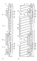
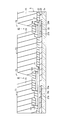
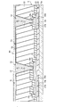
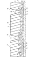
- FIG. 1 is a diagram for explaining a liquid crystal display device according to a first embodiment of the present invention.
- FIG. 2 is a diagram for explaining the configuration of the liquid crystal panel shown in FIG.
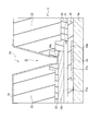
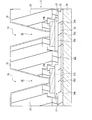
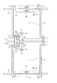
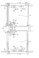
- FIG. 3 is an enlarged plan view for explaining a main configuration of the active matrix substrate shown in FIG. 4 is a cross-sectional view taken along the line IV-IV in FIG. 3, and is a cross-sectional view showing a thin film transistor portion of the active matrix substrate and its vicinity.
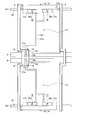
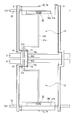
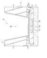
- FIG. 5 is a cross-sectional view showing the auxiliary capacitor portion of the active matrix substrate.
- FIG. 6 is a flowchart showing main manufacturing steps of the main part configuration of the active matrix substrate.
- FIG. 7 is a diagram for explaining a main manufacturing process of the main configuration of the active matrix substrate, and FIGS.
- FIG. 7A to 7B show a series of main manufacturing processes.
- FIG. 8 is a diagram for explaining a main manufacturing process of the main part configuration of the active matrix substrate, and FIGS. 8A to 8B show a series of main manufacturing processes.
- FIG. 9 is a diagram for explaining a main manufacturing process of the main configuration of the active matrix substrate, which is performed subsequent to FIG. 8B, and FIG. 9A to FIG. The main manufacturing process is explained.
- FIG. 10 is a diagram for explaining a main manufacturing process of the main configuration of the active matrix substrate, which is performed subsequent to FIG. 9B, and FIG. 10A to FIG. The main manufacturing process is explained.
- FIG. 11 is a diagram for explaining a main manufacturing process of the main part configuration of the active matrix substrate, which is performed subsequent to FIG.
- FIG. 12 is a diagram for explaining a main manufacturing process of the main configuration of the active matrix substrate, which is performed subsequent to FIG. 11 (b).
- FIG. 12 (a) to FIG. The main manufacturing process is explained.
- FIG. 13 is a diagram for explaining a main manufacturing process of the main part configuration of the active matrix substrate, which is performed subsequent to FIG. 12B.
- FIG. 13A to FIG. The main manufacturing process is explained.
- FIG. 14 is a diagram for explaining a main manufacturing process of the main configuration of the active matrix substrate, which is performed subsequent to FIG.
- FIG. 15 is a diagram for explaining a main manufacturing process of the main configuration of the active matrix substrate, which is performed subsequent to FIG. FIG.
- FIG. 16 is a diagram for explaining the main manufacturing process of the main configuration of the active matrix substrate, which is performed subsequent to FIG.
- FIG. 17 is a diagram for explaining a main manufacturing process of the main configuration of the active matrix substrate, which is performed subsequent to FIG.
- FIG. 18 is a cross-sectional view showing the auxiliary capacity portion in the first comparative example.
- FIG. 19 is a graph showing the relationship between the pixel voltage-auxiliary capacitance wiring voltage and the capacitance ratio.
- FIG. 20 is a cross-sectional view showing the auxiliary capacity portion in the second comparative example.
- FIG. 21 is a graph showing the relationship between the drain electrode-counter electrode and the capacitance ratio.
- FIG. 22 is an enlarged plan view for explaining a main configuration of a modification of the active matrix substrate shown in FIG. FIG.
- FIG. 23 is an enlarged plan view for explaining the main configuration of the active matrix substrate of the liquid crystal panel according to the second embodiment of the present invention.
- FIG. 24 is a cross-sectional view showing an auxiliary capacitor portion of the active matrix substrate shown in FIG.
- FIG. 25 is an enlarged plan view for explaining a main configuration of a modification of the active matrix substrate shown in FIG.
- FIG. 26 is an enlarged plan view for explaining the main configuration of the active matrix substrate of the liquid crystal panel according to the third embodiment of the present invention.
- FIG. 27 is a cross-sectional view showing an auxiliary capacitor portion of the active matrix substrate shown in FIG.
- FIG. 28 is an enlarged plan view for explaining a main configuration of a modification of the active matrix substrate shown in FIG. FIG.
- FIG. 29 is an enlarged plan view for explaining the main configuration of the active matrix substrate of the liquid crystal panel according to the fourth embodiment of the present invention.
- FIG. 30 is a cross-sectional view showing the auxiliary capacitor portion of the active matrix substrate shown in FIG.
- FIG. 31 is an enlarged plan view for explaining a main configuration of another modification of the active matrix substrate shown in FIG.
- FIG. 1 is a diagram for explaining a liquid crystal display device according to a first embodiment of the present invention.
- the liquid crystal display device 1 according to the present embodiment includes a liquid crystal panel 2 in which the upper side of FIG. 1 is installed as a viewing side (display surface side), and a non-display surface side of the liquid crystal panel 2 (lower side of FIG. 1). And a backlight device 3 that generates illumination light for illuminating the liquid crystal panel 2.
- the liquid crystal panel 2 includes a color filter substrate 4 and an active matrix substrate 5 constituting a pair of one and other substrates, respectively, and polarizing plates 6 and 7 provided on the outer surfaces of the color filter substrate 4 and the active matrix substrate 5, respectively. And. A liquid crystal layer LC is sandwiched between the color filter substrate 4 and the active matrix substrate 5. Further, in the liquid crystal panel 2, the liquid crystal layer LC is sealed with a sealing material (not shown).
- the color filter substrate 4 and the active matrix substrate 5 are made of a transparent transparent resin such as a flat transparent glass material or acrylic resin.
- a resin film such as TAC (triacetyl cellulose) or PVA (polyvinyl alcohol) is used, and at least the effective display area A (FIG. 2) of the display surface provided on the liquid crystal panel 2 is provided. It is bonded to the corresponding color filter substrate 4 or active matrix substrate 5 so as to cover it.
- the active matrix substrate 5 pixel electrodes, thin film transistors (TFTs), and the like are formed between the liquid crystal layer LC in accordance with a plurality of pixels included in the display surface of the liquid crystal panel 2 ( Details will be described later.)
- the color filter substrate 4 constitutes a counter substrate, and a color filter layer, an overcoat film, a counter electrode described later, and the like are formed between the color filter substrate 4 and the liquid crystal layer LC. (Not shown).
- the liquid crystal panel 2 is provided with an FPC (Flexible Printed Circuit) 8 connected to a control device (not shown) for controlling the drive of the liquid crystal panel 2, and operates the liquid crystal layer LC in units of pixels.
- FPC Flexible Printed Circuit
- the display surface is driven in units of pixels, and a desired image is displayed on the display surface.
- the liquid crystal mode and pixel structure of the liquid crystal panel 2 are arbitrary. Moreover, the drive mode of the liquid crystal panel 2 is also arbitrary. That is, as the liquid crystal panel 2, any liquid crystal panel that can display information can be used. Therefore, the detailed structure of the liquid crystal panel 2 is not shown in FIG.
- the backlight device 3 includes a light emitting diode 9 as a light source, and a light guide plate 10 disposed to face the light emitting diode 9. Further, in the backlight device 3, the light emitting diode 9 and the light guide plate 10 are sandwiched by the bezel 14 having an L-shaped cross section in a state where the liquid crystal panel 2 is installed above the light guide plate 10. A case 11 is placed on the color filter substrate 4. Thus, the backlight device 3 is assembled to the liquid crystal panel 2 and is integrated as a transmissive liquid crystal display device 1 in which illumination light from the backlight device 3 is incident on the liquid crystal panel 2.
- the light guide plate 10 for example, a synthetic resin such as a transparent acrylic resin is used, and light from the light emitting diode 9 enters.
- a reflection sheet 12 is installed on the opposite side (opposite surface side) of the light guide plate 10 to the liquid crystal panel 2.
- an optical sheet 13 such as a lens sheet or a diffusion sheet is provided on the liquid crystal panel 2 side (light emitting surface side) of the light guide plate 10, and the inside of the light guide plate 10 has a predetermined light guide direction (left side in FIG. 1). The light from the light emitting diode 9 guided in the direction from the right side to the right side is changed to the planar illumination light having uniform luminance and applied to the liquid crystal panel 2.
- the present embodiment is not limited to this, and a direct type backlight device is used. May be.
- a backlight device having other light sources such as a cold cathode fluorescent tube and a hot cathode fluorescent tube other than the light emitting diode can also be used.
- liquid crystal panel 2 of the present embodiment will be specifically described with reference to FIG.
- FIG. 2 is a diagram for explaining the configuration of the liquid crystal panel shown in FIG.
- the liquid crystal display device 1 includes a panel control unit 15 that controls driving of the liquid crystal panel 2 (FIG. 1) as the display unit that displays information such as characters and images, and the panel control.
- a source driver 16 and a gate driver 17 that operate based on an instruction signal from the unit 15 are provided.
- the panel control unit 15 is provided in the control device, and receives a video signal from the outside of the liquid crystal display device 1. Further, the panel control unit 15 performs predetermined image processing on the input video signal to generate each instruction signal to the source driver 16 and the gate driver 17, and the input video signal. A frame buffer 15b capable of storing display data for one frame included. Then, the panel control unit 15 performs drive control of the source driver 16 and the gate driver 17 according to the input video signal, so that information according to the video signal is displayed on the liquid crystal panel 2.
- the source driver 16 and the gate driver 17 are installed on the active matrix substrate 5. Specifically, the source driver 16 is installed on the surface of the active matrix substrate 5 along the lateral direction of the liquid crystal panel 2 in the outer region of the effective display area A of the liquid crystal panel 2 as a display panel. . Further, the gate driver 17 is installed on the surface of the active matrix substrate 5 so as to be along the vertical direction of the liquid crystal panel 2 in the outer region of the effective display region A.
- the effective display area A is provided with a plurality of pixels, and substantially constitutes the display surface of the liquid crystal panel 2.
- the source driver 16 and the gate driver 17 are drive circuits that drive a plurality of pixels P provided on the liquid crystal panel 2 side by pixel.
- the source driver 16 and the gate driver 17 include a plurality of source lines S1 to S1.
- SM is an integer of 2 or more, hereinafter collectively referred to as “S”
- G gate wirings G1 to GN
- S source lines
- G1 to GN gate wirings G1 to GN
- G is an integer of 2 or more and is hereinafter collectively referred to as “G”.
- These source wiring S and gate wiring G constitute a data wiring and a scanning wiring, respectively, on a transparent glass material or a transparent synthetic resin substrate (not shown) included in the active matrix substrate 5.
- the source wiring S is provided on the substrate so as to be parallel to the matrix-like column direction (vertical direction of the liquid crystal panel 2), and the gate wiring G is arranged in the matrix-like row direction (horizontal of the liquid crystal panel 2). Is provided on the substrate so as to be parallel to (direction).
- the source driver 16 is connected to a storage capacitor line CS for generating the storage capacitor Ccs, and the source driver 16 also functions as a drive unit for generating the storage capacitor. It is configured as follows.
- the thin film transistor 18 as a switching element and the pixel P having the pixel electrode 19 connected to the thin film transistor 18 are provided.
- the counter electrode CE provided on the color filter substrate 4 side is configured to face the pixel electrode 19 with the liquid crystal layer LC provided on the liquid crystal panel 2 interposed therebetween. . That is, in the liquid crystal panel 2, at least one thin film transistor 18, at least one pixel electrode 19, and the counter electrode CE are provided for each pixel.
- regions of a plurality of pixels P are formed in each region partitioned in a matrix by the source wiring S and the gate wiring G.
- the plurality of pixels P include red (R), green (G), and blue (B) pixels. These RGB pixels are sequentially arranged in this order, for example, in parallel with the gate wirings G1 to GN. Further, these RGB pixels can display corresponding colors by a color filter layer (not shown) provided on the color filter substrate 4 side.
- the gate driver 17 scans the gate wirings G1 to GN with respect to the gate wirings G1 to GN based on the instruction signal from the image processing unit 15a (gate signal). Signal) in sequence. Further, the source driver 16 supplies a data signal (voltage signal (gradation voltage)) corresponding to the luminance (gradation) of the display image to the corresponding source wirings S1 to SM based on the instruction signal from the image processing unit 15a. Output.
- FIG. 3 is an enlarged plan view for explaining a main configuration of the active matrix substrate shown in FIG. 4 is a cross-sectional view taken along the line IV-IV in FIG. 3, and is a cross-sectional view showing a thin film transistor portion of the active matrix substrate and its vicinity.
- FIG. 5 is a cross-sectional view showing the auxiliary capacitor portion of the active matrix substrate. Note that FIG. 3 illustrates the two pixels P arranged in parallel in the vertical direction and provided symmetrically in the vertical direction.
- the thin film transistor 18 is provided in the vicinity of the intersection of the gate wiring G and the source wiring S.
- the thin film transistor 18 includes a gate electrode 18g integrally formed with the gate line G, a source electrode 18s integrally formed with the source line S, and a drain electrode 18d provided so as to face the source electrode 18s.
- the first semiconductor layer 21a is provided.
- the auxiliary capacitance line CS is provided in parallel with the gate line G.
- the region surrounded by the two source lines S, the gate line G, and the auxiliary capacitance line CS constitutes the area of the pixel P.
- the auxiliary capacitance line CS is provided with a main body CS1 and a thick portion CS2 having a width dimension larger than that of the main body CS1, and an auxiliary capacitance portion T4, which will be described later, is provided on the thick portion CS2. It is configured.
- the pixel P region occupies most of the pixel electrode 19, the thin film transistor portion T 1 in which the thin film transistor 18 is formed, the pixel contact portion T 2 as a connection portion connecting the drain electrode 18 d and the pixel electrode 19, and the pixel electrode 19.
- a pixel portion (that is, an opening portion of the pixel P) T3 that transmits light from the backlight device 3 substantially in the pixel P and an auxiliary capacitance portion T4 that generates an auxiliary capacitance are provided. .
- the thin film transistor portion T1 the pixel contact portion T2, the pixel portion T3, the first, second, third, and fourth masks are used.
- the auxiliary capacitor T4 is formed at the same time.
- the thin film transistor portion T1 includes a base 5a, a gate electrode 18g provided on the base 5a, and a first gate insulation provided so as to cover the base 5a and the gate electrode 18g.
- a film 20a and a first semiconductor layer 21a provided on the first gate insulating film 20a are included.
- the thin film transistor portion T1 includes a source electrode 18s provided on the first semiconductor layer 21a and connected to the first semiconductor layer 21a, and a first electrode provided on the first semiconductor layer 21a.
- a drain electrode 18d connected to the semiconductor layer 21a is included.
- a protective layer 22 provided so as to cover the first gate insulating film 20a, the first semiconductor layer 21a, the source electrode 18s, and the drain electrode 18d, and the protective layer 22 are provided.
- the interlayer insulating film 23 is included.
- the pixel contact portion T2 includes a base material 5a, a first gate insulating film 20a provided on the base material 5a, and a first gate provided on the first gate insulating film 20a.
- the semiconductor layer 21a, the drain electrode 18d and the pixel electrode 19 sequentially provided on the first semiconductor layer 21a are included.
- an opening H1 of a contact hole portion is provided in the protective layer 22 and the interlayer insulating film 23.
- the drain electrode 18d and the pixel electrode are formed in the opening portion H1. 19 is connected.
- the pixel portion T3 includes a base material 5a, a gate insulating film 20 provided on the base material 5a, a protective layer 22 and an interlayer insulating film 23 sequentially provided on the gate insulating film 20. , And a pixel electrode 19.
- the active matrix substrate 5 of the present embodiment has a high aperture ratio SHA (Super High Aperture) structure in which the interlayer insulating film 23 as an intermediate insulating film is provided in the pixel portion T3.
- the source wiring S and the pixel electrode 19 can be overlapped, and the aperture ratio of the pixel portion T3, that is, the aperture ratio of the pixel P can be increased as compared with the case where the interlayer insulating film 23 is not provided.
- SHA Super High Aperture
- the auxiliary capacitance unit T4 also includes the base material 5a, the auxiliary capacitance wiring CS provided on the base material 5a, and the second provided so as to cover the base material 5a and the auxiliary capacitance wiring CS. Gate insulating film 20b.
- a second semiconductor layer 21b provided on the second gate insulating film 20b and a second semiconductor layer 21b provided on the second semiconductor layer 21b are connected to the second semiconductor layer 21b.
- the auxiliary capacitance electrode 24b and the pixel electrode 19 as a transparent electrode connected to the auxiliary capacitance electrode 24b are included.
- auxiliary capacitance portion T4 a plurality of, for example, two opening portions H2 of the contact hole portion are provided in the protective layer 22 and the interlayer insulating film 23.
- auxiliary capacitance portion T4 in each of the opening portions H2.
- the auxiliary capacitance electrode 24b and the pixel electrode 19 are connected.
- each opening H2 is opened with a size smaller than the width of the thick portion CS2 on the thick portion CS2 of the auxiliary capacitance line CS.
- the upper and lower pixels share the auxiliary capacitance line CS with the upper and lower pixels (not shown).
- the liquid crystal panel 2 of the present embodiment as will be described in detail later, an oxide semiconductor is used for the semiconductor layer 21, and the amount of voltage deviation generated in the counter electrode CE is 0.04 (V) or less.
- Ccs ⁇ S / d
- S the area of the electrodes
- d the distance between the electrodes
- ⁇ the dielectric constant of the solvent sandwiched between the electrodes.
- the area S of the auxiliary capacitance Ccs is determined by the overlapping area of the lowermost pixel electrode 19 and the auxiliary capacitance wiring CS of the auxiliary capacitance portion T4.
- the first metal layer includes a plurality of stacked metal films such as a copper film and a titanium film, a copper film and a molybdenum film, or a two-layer metal film such as a copper film and a molybdenum alloy film, or an aluminum film.
- a metal film having a three-layer structure such as a titanium film and an aluminum film or a molybdenum film, an aluminum film, and a molybdenum film is used.
- the gate insulating film 20 is formed by integrally forming a first gate insulating film 20a provided in the thin film transistor portion T1 and a second gate insulating film 20b provided in the auxiliary capacitance portion T4. It is provided so as to cover the first metal layer provided on the material 5a and the base material 5a.
- the gate insulating film 20 is made of, for example, silicon nitride (SiNx) or a laminated film of silicon nitride (SiNx) and silicon oxide (SiO 2 ).
- an oxide semiconductor such as an In—Ga—Zn—O-based amorphous oxide semiconductor is used.
- the semiconductor layer 21 is formed on the gate insulating film 20 so as to cover the entire surface of the gate insulating film 20, and is then etched to perform first etching included in the thin film transistor portion T1 and the pixel contact portion T2.
- the semiconductor layer 21a and the second semiconductor layer 21b included in the auxiliary capacitor T4 (details will be described later).
- the second metal layer formed on the first semiconductor layer 21a is used for the source wiring S, the source electrode 18s, and the drain electrode 18d.
- the second metal layer is a metal film having a two-layer structure such as a copper film and a titanium film, a copper film and a molybdenum film, or a copper film and a molybdenum alloy film, or an aluminum film or titanium.
- a metal film having a three-layer structure such as a film and an aluminum film or a molybdenum film, an aluminum film, and a molybdenum film is used.
- silicon nitride (SiNx), silicon oxide (SiO 2 ), or a laminated film thereof is used for the protective layer 22.
- silicon nitride (SiNx), silicon oxide (SiO 2 ), or a laminated film thereof is used for the protective layer 22.
- the interlayer insulating film 23 a photosensitive interlayer insulating film material in which a photosensitive material is mixed with an insulating material such as a novolac resin is used.
- the pixel electrode 19 is made of a transparent metal oxide film such as ITO or IZO, and is formed so as to cover the interlayer insulating film 23.
- the transparent electrode is configured as the pixel electrode 19 and is included in the auxiliary capacitance unit T4.
- the second semiconductor layer 21 b is located inside the pixel electrode 19.
- the present invention is not limited to this, and the second semiconductor layer 21 b may be located outside the pixel electrode 19.
- the second semiconductor layer 21b is located outside the storage capacitor line CS.
- the present invention is not limited to this, and the second semiconductor layer 21b may be located inside the storage capacitor line CS. It is sufficient that at least the second semiconductor layer 21b is outside the opening H2.
- FIG. 6 is a flowchart showing main manufacturing steps of the main part configuration of the active matrix substrate.
- FIG. 7 is a diagram for explaining a main manufacturing process of the main configuration of the active matrix substrate, and FIGS. 7A to 7B show a series of main manufacturing processes.
- FIG. 8 is a diagram for explaining a main manufacturing process of the main part configuration of the active matrix substrate, and FIGS. 8A to 8B show a series of main manufacturing processes.
- FIG. 9 is a diagram for explaining a main manufacturing process of the main configuration of the active matrix substrate, which is performed subsequent to FIG. 8B, and FIG. 9A to FIG. The main manufacturing process is explained.
- FIG. 10 is a diagram for explaining a main manufacturing process of the main configuration of the active matrix substrate, which is performed subsequent to FIG.
- FIG. 11 is a diagram for explaining a main manufacturing process of the main part configuration of the active matrix substrate, which is performed subsequent to FIG. 10B, and FIG. 11A to FIG.
- the main manufacturing process is explained.
- FIG. 12 is a diagram for explaining a main manufacturing process of the main configuration of the active matrix substrate, which is performed subsequent to FIG. 11 (b).
- the main manufacturing process is explained.
- FIG. 13 is a diagram for explaining a main manufacturing process of the main part configuration of the active matrix substrate, which is performed subsequent to FIG. 12B.
- the main manufacturing process is explained.
- FIG. 14 is a diagram for explaining a main manufacturing process of the main configuration of the active matrix substrate, which is performed subsequent to FIG.
- FIG. 15 is a diagram for explaining a main manufacturing process of the main configuration of the active matrix substrate, which is performed subsequent to FIG.
- FIG. 16 is a diagram for explaining the main manufacturing process of the main configuration of the active matrix substrate, which is performed subsequent to FIG.
- FIG. 17 is a diagram for explaining a main manufacturing process of the main configuration of the active matrix substrate, which is performed subsequent to FIG.
- the first metal layer is first formed on the base material 5a, and then the first mask M1 is formed on the first metal layer.
- the first process of forming the gate electrode 18g of the thin film transistor portion T1 and the auxiliary capacitance line CS of the auxiliary capacitance portion T4 is performed by patterning using (Steps S1 to S4 in FIG. 6).
- step S1 after depositing the first metal layer FM on the base material 5a by using, for example, a sputtering method (step S1), the first mask is formed. Photolithography is performed using M1 and the resist r1 (step S2).
- the gate electrode 18g of the thin film transistor portion T1 and the auxiliary capacitance wiring CS of the auxiliary capacitance portion T4 are formed on the substrate 5a by performing wet etching and patterning (Step). S3).
- step S4 the resist r1 is removed.
- a halftone is applied to the semiconductor layer 21 and the second metal layer 24.
- the second mask M2 made of a mask
- the first semiconductor layer 21a, the source electrode 18s, the drain electrode 18d of the thin film transistor portion T1, and the second semiconductor layer 21b of the auxiliary capacitance portion T4 are formed.
- a second step is performed (steps S5 to S12 in FIG. 6).
- the gate insulating film 20 is deposited so as to cover the gate electrode 18g, the auxiliary capacitance line CS, and the base material 5a by, for example, the CVD method (step S5).
- the first gate insulating film 20a of the thin film transistor portion T1 and the pixel contact portion T2 and the second gate insulating film 20b of the auxiliary capacitance portion T4 are provided.
- the semiconductor layer 21 is deposited on the gate insulating film 20 by, for example, sputtering (step S5).
- the first semiconductor layer 21a of the thin film transistor portion T1 and the pixel contact portion T2 and the second semiconductor layer 21b of the auxiliary capacitance portion T4 are provided.
- the second metal layer 24 is deposited on the semiconductor layer 21 by using, for example, a sputtering method (step S6).
- the second mask M2 is a halftone mask that forms a three-tone resist pattern having no resist, a thin resist film (resist half 25b), and a thick resist film (resist full 25a). ing. That is, the second mask M2 is provided with, for example, three portions M2a, M2b, and M2c having different transmittances. On the second metal layer 24, as shown in FIG. Corresponding to these portions M2a, M2b, and M2c, a portion without the resist 25, a portion of the resist full 25a where the resist 25 is thick, and a portion of the resist half 25b where the resist 25 is thin are formed.
- a gray tone mask that forms a portion of the resist half 25b by providing a plurality of slits may be used.
- step S8 wet etching is performed to leave the portion of the second metal layer 24 covered with the resist 25, and the thin film transistor portion T1 and the pixel contact portion T2.
- the first second metal layer 24a and the auxiliary capacitance electrode 24b of the auxiliary capacitance portion T4 are formed (step S8).
- step S9 wet etching is performed to leave the portion of the semiconductor layer 21 covered with the resist 25, and the first portions of the thin film transistor portion T1 and the pixel contact portion T2 are left.
- the semiconductor layer 21a and the second semiconductor layer 21b of the auxiliary capacitance unit T4 are formed (step S9).
- step S9 the portion of the semiconductor layer 21 (second semiconductor layer 21b) covered with the resist 25 is also formed in the auxiliary capacitance portion T4 (step S9).
- wet etching on the second metal layer 24 and the semiconductor layer 21 may be performed simultaneously.
- step S10 the resist half 25b is removed by performing, for example, ashing.
- wet etching is performed to leave a portion of the first second metal layer 24a covered with the resist full 25a, and the source electrode of the thin film transistor portion T1. 18s and the drain electrode 18d of the thin film transistor portion T1 and the pixel contact portion T2 are formed (step S11). Further, in the auxiliary capacitance portion T4, since the auxiliary capacitance electrode 24b is covered with the resist full 25a, it is left without being removed.
- step S12 the resist full 25a is peeled off.
- annealing may be performed at 200 ° C. to 400 ° C. in order to stabilize the first semiconductor layer 21a and the second semiconductor layer 21b.
- the first semiconductor layer 21a is formed around the source electrode 18s and the drain electrode 18d so as to surround them.
- the first gate insulating film 20a, the first semiconductor layer 21a, the source electrode 18s, the drain electrode 18d, the second gate insulating film 20b, the second semiconductor layer 21b, and the auxiliary capacitance electrode 24b are covered.
- patterning is performed using the third mask M3 to form openings H1 and H2 in the protective layer 22 and the interlayer insulating film 23, and the gate wiring G
- a third step is performed on the opening (not shown) of the terminal portion in the gate insulating film 20, the protective layer 22, and the interlayer insulating film 23 (steps S13 to S16 in FIG. 6).
- the protective layer 22 covers the gate insulating film 20, the semiconductor layer 21, the source electrode 18s, the drain electrode 18d, and the auxiliary capacitance electrode 24b by, for example, the CVD method. In this manner, the deposit is made (step S13).
- step S14 after the interlayer insulating film 23 is applied on the protective layer 22 (step S14), photolithography is performed using the third mask M3 (step S15).
- step S15 the contact hole portion opening H1 is formed in the interlayer insulating film 23 in the pixel contact portion T2
- the contact hole portion opening H2 is formed in the interlayer insulating film 23 in the auxiliary capacitor portion T4.
- the protective layer 22 and the interlayer insulating film 23 of the thin film transistor portion T1 are formed.
- the openings H1 and H2 are also formed in the protective layer 22, respectively, and the openings H1 and H2 are completed (step S16).
- the gate insulating film and the protective layer are etched to open the terminal portion (not shown).
- annealing may be performed at 200 ° C. to 400 ° C. in order to stabilize the first semiconductor layer 21a and the second semiconductor layer 21b.
- the pixel electrode 19 as a transparent electrode is formed on the drain electrode 18d, the auxiliary capacitance electrode 24b, the protective layer 22, and the interlayer insulating film 23 by using, for example, a sputtering method. Deposited (step S17). Thereafter, photolithography is performed using the fourth mask M4 and the resist r2 (step S18).
- the transparent electrode (pixel electrode 19) of the auxiliary capacitor T4 is formed by performing wet etching and patterning (step S19).
- step S20 the resist r2 is stripped.
- the active matrix substrate 5 of the present embodiment is completed through the above first to fourth steps.
- the liquid crystal panel 2 of the present embodiment as described above, an oxide semiconductor is used for the semiconductor layer 21 and the amount of voltage deviation generated in the counter electrode CE is 0.04 (V) or less. Thereby, in the liquid crystal panel 2 of this embodiment, it is possible to prevent the liquid crystal panel 2 from being seized even when the auxiliary capacity of the auxiliary capacity unit T4 varies.
- the ratio of the area of the second semiconductor layer 21b to the area of the auxiliary capacitor T4 (that is, the auxiliary when viewed in plan from the upper side of the opening H2).
- p be the ratio of the area of the second semiconductor layer 21b in the capacitor T4.
- the capacitance between the gate electrode 18g and the drain electrode 18d is Cgd
- the capacitance of the liquid crystal layer LC is Clc
- the auxiliary capacitance of the auxiliary capacitance portion T4 is Ccs.
- the value of Cgd / (Cgd + Clc + Ccs) is ⁇
- the ratio of the auxiliary capacitance by the second gate insulating film 20b to the auxiliary capacitance of the auxiliary capacitance portion T4 is ⁇ .
- the voltage deviation amount ⁇ Vd ′ generated in the counter electrode CE is obtained by the following equation (1).
- the auxiliary capacitance ratio ⁇ is such that the dielectric constants of the second gate insulating film 20b and the second semiconductor layer 21b are ⁇ GI and ⁇ i, respectively, and the film of the second gate insulating film 20b and the second semiconductor layer 21b.
- the thicknesses are dGI and di, respectively, the following equation (3) is obtained.
- each part of the liquid crystal panel 2 is configured so that the voltage deviation amount ⁇ Vd ′ is 0.04 (V) or less, and the liquid crystal panel 2 is seized. It is comprised so that it can prevent.
- an oxide semiconductor is used for the second semiconductor layer 21b of the auxiliary capacitance unit T4. Therefore, the auxiliary capacitance electrode formed on the second semiconductor layer 21b.
- 24b takes in the oxide of the second semiconductor layer 21b, a low-resistance interface is generated at the interface between the second semiconductor layer 21b and the auxiliary capacitance electrode 24b.
- the auxiliary capacity of the auxiliary capacity unit T4 varies.
- the source voltage is applied to the corresponding pixel electrode 19. Is written. However, the voltage written to the pixel electrode 19 is smaller than the source voltage.
- “+ write” and “ ⁇ write” as used herein refer to the case where the source driver 16 is configured to apply a voltage of, for example, 0 V or more and 15 V or less to the source electrode 18s. A case where a large voltage and a small voltage are applied as source voltages, respectively.
- the voltage written to the pixel electrode 19 changes by the following ⁇ Vd (pull-in voltage) as compared with the source voltage when the gate voltage to the gate electrode 18g is switched from the high voltage to the low voltage.
- the adjustment value Vcom1 of the counter voltage Vcom is obtained by the average value of “+ write” and “ ⁇ write” described above, and is expressed by the following equation (5).
- the threshold value in the second semiconductor layer 21b changes to, for example, the “ ⁇ write” side.
- the auxiliary capacitance unit T4 the auxiliary capacitance changes as the liquid crystal panel 2 is used.
- the adjustment value Vcom2 of the counter voltage Vcom after use of the liquid crystal panel 2 is expressed by the following equation (6).
- the voltage deviation amount ⁇ Vd ′ generated in the counter electrode CE after the use of the liquid crystal panel 2 is obtained by subtracting the equation (6) from the equation (5).
- the voltage deviation amount ⁇ Vd ′ is expressed by the above equation (1).
- the liquid crystal panel 2 of this embodiment when the voltage deviation amount ⁇ Vd ′ exceeds 0.04 (V), the liquid crystal panel 2 is seized. That is, in the liquid crystal panel 2, even if a voltage is written to the pixel electrode 19 and a voltage is applied to the liquid crystal layer LC, the liquid crystal panel 2 is baked without tilting the liquid crystal molecules of the liquid crystal layer LC.
- FIG. 18 is a cross-sectional view showing the auxiliary capacity portion in the first comparative example.
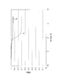
- FIG. 19 is a graph showing the relationship between the pixel voltage-auxiliary capacitance wiring voltage and the capacitance ratio.
- FIG. 20 is a cross-sectional view showing the auxiliary capacity portion in the second comparative example.
- FIG. 21 is a graph showing the relationship between the drain electrode-counter electrode and the capacitance ratio.
- Table 1, Table 2, and Table 3 show specific examples of test results of the present embodiment product.
- the number of pixels in the effective display area A corresponds to FHD (Full High Definition), QXGA (Quad eXtended Graphics Array), and QFHD (Quad Full High Definition), respectively. It is a thing. That is, in the present embodiment in Table 1, Table 2, and Table 3, the number of pixels in the effective display area A is set to (1080 ⁇ 1920 dots), (1536 ⁇ 2048 dots), and (2160 ⁇ 3840 dots), respectively.
- the voltage deviation amount ⁇ Vd ′ is The seizure occurred at 0.08 (V).
- the size of the effective display area A is 21 inches or more, it has been confirmed that the voltage deviation amount ⁇ Vd ′ is 0.04 (V) or less and the occurrence of seizure can be reliably prevented.
- the size of the effective display area A is 10 inches, 21 inches, and 32 inches.
- the voltage deviation amount ⁇ Vd ′ was 0.09 (V), 0.07 (V), and 0.05 (V), respectively, and seizure occurred.
- the size of the effective display area A is 46 inches or more, it has been confirmed that the voltage deviation amount ⁇ Vd ′ is 0.04 (V) or less and the occurrence of seizure can be surely prevented.
- the auxiliary capacitance wiring CS ′, the gate insulating film 20 ′, and the second semiconductor layer 26b ′ are sequentially formed on the base material 5a ′.
- the second semiconductor layer 26b ′ is constituted by a semiconductor layer 26 ′ made of, for example, an amorphous silicon layer (i layer).
- an electrode contact layer 27 ′ made of, for example, an n + layer is provided on the second semiconductor layer 26b ′, and further, a drain electrode (to cover the second semiconductor layer 26b ′ and the electrode contact layer 27 ′).
- a storage capacitor electrode) 24b ' is formed.
- a protective layer 22 ′ and an interlayer insulating film 23 ′ are sequentially formed so as to cover the gate insulating film 20 ′ and the drain electrode 24b ′.
- the protective layer 22 ′ and the interlayer insulating film 23 ′ are provided with an opening H4 ′ of a contact hole portion, and the pixel electrode 19 ′ and the drain electrode 24b ′ are connected in the opening H4 ′. Has been.
- the auxiliary capacitance is the auxiliary capacitance wiring CS ′, the second gate insulating film 20b ′ sequentially provided thereabove, the second capacitance.
- the auxiliary capacitor portion T4 ′ is formed by using the four first to fourth masks M1 to M4 as in the case of the present embodiment product.
- Table 4 Table 5, and Table 6.
- Table 5 Table 5 and Table 6
- the number of pixels in the effective display area A corresponds to the above-described FHD, QXGA, and QFHD, respectively, as in the present embodiment product.
- an oxide semiconductor is used for the second semiconductor layer 21b
- an amorphous silicon layer is used for the second semiconductor layer 26b ′.
- An electrode contact layer 27 ′ is formed so as to cover the upper surface of the second semiconductor layer 26b ′.
- the electrode contact layer 27 ′ and the second semiconductor layer 26b are connected from the pixel electrode 19 ′ through the drain electrode 24b ′ along with the use of the liquid crystal panel 2 (that is, with aging).
- the threshold value of the second semiconductor layer 26b' changes, causing a change in the auxiliary capacitance of the auxiliary capacitance portion T4 '. As a result, the liquid crystal panel 2 is seized.
- the curves 60 and 61 are the first comparative example before (initial value) and after the change (after aging with the screen continuously displayed), respectively.
- the relationship between the pixel voltage-auxiliary capacitance wiring voltage and the (auxiliary) capacitance ratio is shown.
- the above-mentioned “+ write” and “ ⁇ write” are performed on the pixel when the pixel voltage-auxiliary capacitance wiring voltage is larger than 0 and smaller than 0, respectively. It corresponds.
- the curve 61 is further shifted to the left.
- the auxiliary capacitance Ccs varies depending on + write and -write, and is specifically expressed by the following equations (7) and (8), respectively.
- dGI and ⁇ GI are the film thickness and dielectric constant of the second gate insulating film 20b ', respectively.
- di and ⁇ i are the film thickness and dielectric constant of the second semiconductor layer 26b ', respectively.
- S is the area of the auxiliary capacitor Ccs.
- the ⁇ write auxiliary capacitance Ccs ⁇ is equal to the case where the auxiliary capacitance portion is formed only by the second gate insulating film 20b ′, and the value thereof is larger than the + write auxiliary capacitance.
- the threshold value in the second semiconductor layer 26b ′ is increased due to the presence of the electrode contact layer 27 ′ as the liquid crystal panel 2 is used. It changes to the “write” side.
- the auxiliary capacitance unit T4 ' the auxiliary capacitance changes with use of the liquid crystal panel 2 as described later.
- the threshold value in the second semiconductor layer 26b ' changes in the + direction depending on the process conditions of the second semiconductor layer 26b'.
- the threshold value in the second semiconductor layer 26b ′ becomes “ ⁇ write” side due to the presence of the electrode contact layer 27 ′ and the second semiconductor layer 26b ′.
- the auxiliary capacity changes when the value changes to.
- the pull-in voltage ⁇ Vd changes and the counter voltage (common potential) Vcom also shifts as shown in the above equation (4).
- the voltage deviation amount ⁇ Vd ′ becomes larger than 0.04 (v), and seizure occurs.
- the storage capacitor line CS ′′, the gate insulating film 20 ′′, and the second semiconductor layer 26b ′′ are sequentially formed on the base material 5a ′′.
- the second semiconductor layer 26b ′′ is composed of, for example, a semiconductor layer 26 ′′ made of an amorphous silicon layer (i layer).
- an electrode contact layer 27 ′′ made of an n + layer is provided, and a drain electrode (auxiliary capacitance electrode) 24b ′′ is connected to the electrode contact layer 27 ′′.
- the active matrix substrate 5 ′′ of the second comparative example is also provided.
- a protective layer 22 ′′ and an interlayer insulating film 23 ′′ are sequentially formed so as to cover the gate insulating film 20 ′′, the second semiconductor layer 26b ′′, and the drain electrode 24b ′′.
- the protective layer 22 ′′ and the interlayer insulating film 23 ′′ are provided with an opening H2 ′ of the contact hole portion, and the pixel electrode 19 ′′ and the drain electrode 24b ′′ are connected in the opening H2 ′. ing.
- the auxiliary capacitance is the auxiliary capacitance wiring CS ′′, the second gate insulating film 20b ′′ sequentially provided thereabove, the second capacitance The portion between the semiconductor layer 26b ′′, the electrode contact layer 27 ′′, and the drain electrode 24b ′′, the storage capacitor line CS ′′, and the second gate insulating film 20b ′′ and the drain electrode 24b ′′ that are sequentially provided thereabove. It is comprised so that it may occur in the part between. Further, this auxiliary capacitor T4 ′′ is formed by using five masks unlike the product of the present embodiment.
- Table 7 shows specific examples of test results in the second comparative example.
- the voltage deviation amount ⁇ Vd ′ in the prototype 1 and the prototype 2 was a value exceeding 0.04 (V), and seizure occurred.
- the voltage deviation amount ⁇ Vd ′ in trial production 3 to trial production 8 was 0.04 (V) or less and no seizure occurred.
- the second comparative example is formed using five masks as described above, the manufacturing process is complicated as compared with the present embodiment product formed using four masks. In addition, it is difficult to reduce the manufacturing time and the manufacturing cost. Further, in the second comparative example, there is a problem that the degree of freedom in designing the liquid crystal panel is low as compared with the product of the present embodiment.
- the storage capacitor portion T4 ′′ is compared with the product of the present embodiment.
- the capacity change was large. More specifically, as shown by a curve 71 in FIG. 21, the capacity change is larger than that of the present embodiment product shown by a curve 70 in FIG.
- the second semiconductor layer 21b has a higher (charge) mobility than those of the second semiconductor layers 26b ′ and 26b ′′.
- the mobility of the second semiconductor layer 21b is 5 or more, whereas the mobility of the second semiconductor layers 26b ′ and 26b ′′ is about 0.3.
- the film thickness (for example, about 200 to 800 mm) of the second semiconductor layer 21b can be made thinner than the film thickness (for example, about 2000 to 3000 mm) of the second semiconductor layers 26b ′ and 26b ′′. .
- the relative dielectric constant is as large as about 15 for an oxide semiconductor and about 15 for an amorphous silicon layer.
- the value of ⁇ can be made larger than that of the second semiconductor layers 26b ′ and 26b ′′. That is, in the product of this embodiment, the curve 70 in FIG. As shown, the value of the capacity ratio ⁇ can be about 0.95. As shown by the curve 71 in FIG. 16, the value of the capacity ratio ⁇ of the second semiconductor layers 26b ′ and 26b ′′ is 0.70. Can be larger than the degree.
- the value of ⁇ Vg can be reduced.
- the off current Ioff of the second semiconductor layer 21b is about 1 ⁇ 10 ⁇ 12 to 1 ⁇ 10 ⁇ 14 (A)
- the off current Ioff of the second semiconductor layers 26b ′ and 26b ′′ is 1 ⁇ 10 ⁇ 9 to 1 ⁇ 10. -11 (A)
- ⁇ Vg can be about 20 to 35 (V)
- ⁇ Vg needs to be about 40 (V).
- the voltage deviation amount ⁇ Vd ′ can be made smaller than in the first and second comparative examples, and the occurrence of seizure can be prevented. can do.
- the thin film transistor unit T1 includes the base material 5a, the gate electrode 18g sequentially provided on the base material 5a, the first gate insulating film 20a, and the first semiconductor.
- a layer 21a, a source electrode 18s and a drain electrode 18d, a protective layer 22, and an interlayer insulating film 23 are included.
- the auxiliary capacitance portion T4 includes a base material 5a, an auxiliary capacity wiring CS sequentially provided on the base material 5a, a second gate insulating film 20b, a second semiconductor layer 21b, an auxiliary capacity electrode 24b, and a pixel.
- An electrode (transparent electrode) 19 is included.
- the active matrix substrate 5 having the thin film transistor portion T1 and the auxiliary capacitance portion T4 can be appropriately configured using four masks. Furthermore, in the liquid crystal panel 2 of the present embodiment, the second semiconductor layer 21b made of an oxide semiconductor is used, and the voltage deviation amount ⁇ Vd ′ generated in the counter electrode CE is set to 0.04 (V) or less. Thus, in the present embodiment, unlike the conventional example, it is possible to provide an inexpensive liquid crystal panel 2 that can prevent the occurrence of seizure even when the auxiliary capacity of the auxiliary capacity unit T4 varies.
- the first metal layer FM formed on the base material 5a is used for the gate electrode 18g and the auxiliary capacitance wiring CS. Accordingly, in the present embodiment, the gate electrode 18g and the auxiliary capacitance line CS can be configured using the same first metal layer FM, and the liquid crystal panel 2 that is easier to manufacture and less expensive can be configured. .
- the second metal layer 24 formed on the first or second semiconductor layer 21a, 21b is used for the source electrode 18s, the drain electrode 18d, and the auxiliary capacitance electrode 24b. Accordingly, in the present embodiment, the source electrode 18s, the drain electrode 18d, and the auxiliary capacitance electrode 24b can be configured using the same second metal layer 24, and the liquid crystal panel 2 that is easier to manufacture and less expensive can be obtained. Can be configured.
- the first and second gate insulating films 20a and 20b are integrally formed.
- the liquid crystal panel 2 which is easier to manufacture and less expensive can be configured.
- the pixel electrode (transparent electrode) 19 is connected to the auxiliary capacitance electrode 24b in the opening H2 provided in the protective layer 22 and the interlayer insulating film 23.
- the liquid crystal panel 2 which is easier to manufacture and less expensive can be configured.
- auxiliary capacitance unit T4 in the auxiliary capacitance unit T4, one second semiconductor layer 21b, an auxiliary capacitance electrode 24b, and an opening H2 are provided on the thick portion CS2. But you can.
- FIG. 23 is an enlarged plan view for explaining the main configuration of the active matrix substrate of the liquid crystal panel according to the second embodiment of the present invention.
- FIG. 24 is a cross-sectional view showing an auxiliary capacitor portion of the active matrix substrate shown in FIG.
- the main difference between this embodiment and the first embodiment is that the first and second semiconductor layers are integrally formed, and the drain electrode and the auxiliary capacitance electrode are integrally formed. Is a point.
- symbol is attached
- the drain electrode 18d and the auxiliary capacitance electrode 24b are integrally configured in the second step.
- the first and second semiconductor layers 21a and 21b are integrally formed below the integrally formed drain electrode 18d and auxiliary capacitance electrode 24b.
- the semiconductor layers 21a and 21b, the drain electrode 18d and the auxiliary capacitance electrode 24b which are integrally formed are included.
- the present embodiment can achieve the same operations and effects as the first embodiment.
- the first and second semiconductor layers 21a and 21b are integrally formed, and the drain electrode 18d and the auxiliary capacitance electrode 24b are integrally formed.
- the installation number of the opening part of a contact hole part can be reduced, and the cost-effective liquid crystal panel 2 can be comprised easily.
- each of the two auxiliary capacitance electrodes 24b of the auxiliary capacitance portion T4 is electrically connected by the drain electrode 18d configured integrally, one of the auxiliary capacitance electrodes 24b has a foreign object between the auxiliary capacitance wiring CS. Even if a leak occurs due to the occurrence of this, the drain electrode 18d integrally formed with the leaked auxiliary capacitance electrode 24b can be laser-cut normally to increase the yield.
- auxiliary capacitance unit T4 in the auxiliary capacitance unit T4, one second semiconductor layer 21b, an auxiliary capacitance electrode 24b, and an opening H2 are provided on the thick portion CS2. But you can.
- FIG. 26 is an enlarged plan view for explaining the main configuration of the active matrix substrate of the liquid crystal panel according to the third embodiment of the present invention.
- FIG. 27 is a cross-sectional view showing an auxiliary capacitor portion of the active matrix substrate shown in FIG.
- the main difference between the present embodiment and the first embodiment is that an auxiliary capacitance electrode is provided in the auxiliary capacitance portion so as to be larger than the opposing portion of the auxiliary capacitance wiring.
- an auxiliary capacitance electrode is provided in the auxiliary capacitance portion so as to be larger than the opposing portion of the auxiliary capacitance wiring.
- the slit CS3 is formed in the width direction of the thick portion CS2 (upper and lower sides in FIG. 26) in the first step. Direction).
- the second gate insulating film 20b, the second semiconductor layer 21b, the auxiliary capacitance electrode 24b, and the pixel electrode (transparent electrode) 19 are sequentially provided on the thick width portion CS2.
- the auxiliary capacitance electrode 24b is provided so as to be larger than the opposing portion of the auxiliary capacitance wiring CS.
- the present embodiment can achieve the same operations and effects as the first embodiment.
- the auxiliary capacitance electrode 24b is provided larger than the portion where the auxiliary capacitance line CS is opposed.
- the facing area of the auxiliary capacitance line CS can be used as an auxiliary capacitance generation portion with certainty, and the reduction of the auxiliary capacitance of the auxiliary capacitance unit T4 is reliably prevented. be able to.
- the auxiliary capacitance Ccs is determined by the process accuracy of the first step. Variations in the capacitance Ccs can be reduced. That is, it is possible to reliably prevent the influence of each manufacturing variation of the protective layer 22 provided with the opening H2 and the interlayer insulating film 23 from appearing in the auxiliary capacitance portion T4, and to form the auxiliary capacitance portion T4 with high accuracy. A decrease in the auxiliary capacity Ccs of the auxiliary capacity unit T4 can be reliably prevented.
- auxiliary capacitance unit T4 in the auxiliary capacitance unit T4, one second semiconductor layer 21b, an auxiliary capacitance electrode 24b, and an opening H2 are provided on the thick portion CS2. But you can.
- FIG. 29 is an enlarged plan view for explaining the main configuration of the active matrix substrate of the liquid crystal panel according to the fourth embodiment of the present invention.
- FIG. 30 is a cross-sectional view showing the auxiliary capacitor portion of the active matrix substrate shown in FIG.
- the main difference between the present embodiment and the first embodiment is that a branch wiring branched to the thin film transistor portion side is provided in the auxiliary capacitance wiring, and the second gate insulating film, The second semiconductor layer, the auxiliary capacitance electrode, and the second transparent electrode are sequentially provided.
- symbol is attached
- auxiliary capacitance wiring CS of the active matrix substrate 5 of the present embodiment a plurality of, for example, two branch wirings CS4 are provided in the first step.
- Each of these branch lines CS4 is provided so as to branch to the thin film transistor portion T1 side as shown in FIG.
- auxiliary capacitance portions T4 are formed corresponding to the two branch wirings CS4, respectively. That is, in each auxiliary capacitance unit T4, the second gate insulating film 20b, the second semiconductor layer 21b, the auxiliary capacitance electrode 24b, and the pixel electrode (transparent electrode) 19 are sequentially provided on the branch wiring CS4. The pixel electrode 19 is connected to the auxiliary capacitance electrode 24b inside the opening H2a.
- the present embodiment can achieve the same operations and effects as the first embodiment. Further, in the present embodiment, by providing two branch lines CS4 in the auxiliary capacity line CS, the total auxiliary capacity of the two auxiliary capacity units T4 (that is, the auxiliary capacity in pixel units) can be easily increased. it can. Even if one of the auxiliary capacitance portions T4 leaks due to the generation of a foreign substance between the branch wiring CS4 of the auxiliary capacitance wiring CS and the auxiliary capacitance electrode 24b, the branch wiring CS4 of the leaked auxiliary capacitance wiring CS is laser-cut. By doing so, it is possible to light normally and increase the yield.
- the variation of the auxiliary capacitance Ccs can be reduced by determining the variation of the auxiliary capacitance Ccs by the process accuracy of the first step. That is, it is possible to reliably prevent the influence of each manufacturing variation of the protective layer 22 provided with the opening H2a and the interlayer insulating film 23 from appearing in the auxiliary capacitance portion T4, and to form the auxiliary capacitance portion T4 with high accuracy. A decrease in the auxiliary capacity Ccs of the auxiliary capacity unit T4 can be reliably prevented.
- the auxiliary capacitance electrode 24b may not be configured to cover all the branch wirings CS4, but may be configured to cover only the branch wiring CS4 on one long side.
- the protective layer and the interlayer insulating film are not limited to one layer, and may be two or more layers.
- the shape which further comprises an insulating film on a pixel electrode may be sufficient.
- the present invention is not limited to this, and for example, the auxiliary capacitor is used for the gate driver as the driving unit.
- a configuration may be employed in which the auxiliary capacitance is generated by connecting the wiring or by connecting to a drive unit (driver) dedicated to the auxiliary capacitance wiring.
- the gate wiring G may be configured to be shared by the upper and lower pixels P.
- each of the upper and lower sub-pixels is a sub-pixel, and two pixels form one pixel.
- the upper pixel is a bright pixel and the lower pixel is a dark pixel, thereby improving the viewing angle.
- different potentials are inputted to the upper and lower pixels as the potential of the auxiliary capacitance line CS.
- the storage capacitor line CS corresponding to the upper subpixel has a potential of 1V
- the storage capacitor line CS corresponding to the lower subpixel has a potential of -1V.
- Due to the auxiliary capacitance the upper sub-pixel becomes larger than the written potential, and the lower sub-pixel becomes smaller than the written potential.
- the viewing angle can be improved.
- a plurality of thin film transistors may be provided in the thin film transistor portion.
- the present invention is useful for a low-cost liquid crystal panel capable of reducing the number of masks and preventing the occurrence of image sticking, and a manufacturing method thereof.
Landscapes
- Physics & Mathematics (AREA)
- Engineering & Computer Science (AREA)
- Nonlinear Science (AREA)
- Power Engineering (AREA)
- Microelectronics & Electronic Packaging (AREA)
- Mathematical Physics (AREA)
- Chemical & Material Sciences (AREA)
- Crystallography & Structural Chemistry (AREA)
- General Physics & Mathematics (AREA)
- Optics & Photonics (AREA)
- Liquid Crystal (AREA)
Abstract
薄膜トランジスタ部(T1)及び補助容量部(T4)が設けられたアクティブマトリクス基板(5)と、対向電極(CE)が設けられたカラーフィルタ基板(対向基板)(4)と、アクティブマトリクス基板(5)とカラーフィルタ基板(4)との間に設けられた液晶層(LC)とを有する液晶パネル(2)において、酸化物半導体からなる第2の半導体層(21b)を補助容量部(T4)に設ける。さらに、対向電極(CE)に生じる電圧ズレ量ΔVd'を、0.04(V)以下とする。
Description
本発明は、液晶パネル、及びその製造方法に関する。
近年、例えば液晶表示装置は、在来のブラウン管に比べて薄型、軽量などの特長を有するフラットパネルディスプレイとして、液晶テレビ、モニター、携帯電話などに幅広く利用されている。このような液晶表示装置では、複数のソース配線(データ配線)及び複数のゲート配線(走査配線)をマトリクス状に配線するとともに、ソース配線とゲート配線との交差部の近傍にスイッチング素子としての薄膜トランジスタ(TFT:Thin Film Transistor)と、この薄膜トランジスタに接続された画素電極を有する画素をマトリクス状に配置したアクティブマトリクス基板を、表示パネルとしての液晶パネルに用いたものが知られている。
また、上記のようなアクティブマトリクス基板では、一般的に、補助容量配線がゲート配線と平行に設けられており、画素毎に補助容量部を設けて、所定の補助容量を発生するように構成されている。
また、従来の液晶パネルでは、例えば下記特許文献1に記載されているように、5枚のマスクを使用して、そのアクティブマトリクス基板上の各部、つまりソース配線、ゲート配線、あるいは薄膜トランジスタが形成された薄膜トランジスタ部、または補助容量を発生する補助容量部等を形成していた。
しかしながら、上記のような従来の液晶パネルでは、5枚のマスクを用いて、薄膜トランジスタ部や補助容量部等のアクティブマトリクス基板の各部を形成していた。このため、この従来の液晶パネルでは、そのアクティブマトリクス基板の製造に要するマスク枚数が多くて、当該マスク枚数を低減することが難しいという問題点があった。この結果、この従来の液晶パネルでは、その製造歩留まりの向上を図ったり、製造時間の短縮を図ったり、低コスト化を図ったりするのが困難であった。
また、上記のような従来の液晶パネルでは、補助容量部の補助容量の変動に起因して当該液晶パネルに焼付きが発生するのを防止できないことがあった。すなわち、従来の液晶パネルでは、薄膜トランジスタのソース電極への電圧印加に応じて、補助容量部の補助容量が変動することがあった。また、従来の液晶パネルでは、この補助容量部の補助容量の変動により、アクティブマトリクス基板に対向する対向基板(カラーフィルタ基板)側に設けられた対向電極に生じる電圧が例えば工場出荷時での初期値よりズレを生じることがあった。この結果、従来の液晶パネルでは、その液晶層に電圧印加を行っても、当該液晶層の液晶分子が傾動せずに、当該液晶パネルに焼付きが発生することがあった。
上記の課題を鑑み、本発明は、マスク枚数を低減することができるとともに、焼付きの発生を防止することができるコスト安価な液晶パネル、及びその製造方法を提供することを目的とする。
上記の目的を達成するために、本発明にかかる液晶パネルは、複数の画素が設けられるとともに、前記複数の画素毎に薄膜トランジスタが形成された薄膜トランジスタ部及び補助容量を発生する補助容量部が設けられたアクティブマトリクス基板と、対向電極が設けられた対向基板と、前記アクティブマトリクス基板と前記対向基板との間に設けられた液晶層とを有する液晶パネルであって、
前記薄膜トランジスタ部は、基材と、前記基材上に設けられたゲート電極と、前記基材及び前記ゲート電極を覆うように設けられた第1のゲート絶縁膜と、前記第1のゲート絶縁膜上に設けられるとともに、酸化物半導体からなる第1の半導体層と、前記第1の半導体層上に設けられて当該第1の半導体層に接続されたソース電極と、前記第1の半導体層上に設けられて当該第1の半導体層に接続されたドレイン電極と、前記第1のゲート絶縁膜、前記第1の半導体層、前記ソース電極、及び前記ドレイン電極を覆うように設けられた保護層と、前記保護層上に設けられた層間絶縁膜とを含んで構成され、
前記補助容量部は、前記基材と、前記基材上に設けられた補助容量配線と、前記基材及び前記補助容量配線を覆うように設けられた第2のゲート絶縁膜と、前記第2のゲート絶縁膜上に設けられるとともに、酸化物半導体からなる第2の半導体層と、前記第2の半導体層上に設けられて当該第2の半導体層に接続された補助容量電極と、前記補助容量電極に接続された透明電極とを含んで構成され、
前記補助容量部の面積での前記第2の半導体層の面積の割合をpとし、前記ゲート電極と前記ドレイン電極との間の静電容量をCgdとし、前記液晶層の静電容量をClcとし、前記補助容量部の補助容量をCcsとし、Cgd/(Cgd+Clc+Ccs)の値をβとし、前記補助容量部の補助容量に対する前記第2のゲート絶縁膜による補助容量の比をγとし、前記ゲート電極へのオン電圧とオフ電圧との電圧差をΔVgとしたときに、
前記薄膜トランジスタ部は、基材と、前記基材上に設けられたゲート電極と、前記基材及び前記ゲート電極を覆うように設けられた第1のゲート絶縁膜と、前記第1のゲート絶縁膜上に設けられるとともに、酸化物半導体からなる第1の半導体層と、前記第1の半導体層上に設けられて当該第1の半導体層に接続されたソース電極と、前記第1の半導体層上に設けられて当該第1の半導体層に接続されたドレイン電極と、前記第1のゲート絶縁膜、前記第1の半導体層、前記ソース電極、及び前記ドレイン電極を覆うように設けられた保護層と、前記保護層上に設けられた層間絶縁膜とを含んで構成され、
前記補助容量部は、前記基材と、前記基材上に設けられた補助容量配線と、前記基材及び前記補助容量配線を覆うように設けられた第2のゲート絶縁膜と、前記第2のゲート絶縁膜上に設けられるとともに、酸化物半導体からなる第2の半導体層と、前記第2の半導体層上に設けられて当該第2の半導体層に接続された補助容量電極と、前記補助容量電極に接続された透明電極とを含んで構成され、
前記補助容量部の面積での前記第2の半導体層の面積の割合をpとし、前記ゲート電極と前記ドレイン電極との間の静電容量をCgdとし、前記液晶層の静電容量をClcとし、前記補助容量部の補助容量をCcsとし、Cgd/(Cgd+Clc+Ccs)の値をβとし、前記補助容量部の補助容量に対する前記第2のゲート絶縁膜による補助容量の比をγとし、前記ゲート電極へのオン電圧とオフ電圧との電圧差をΔVgとしたときに、

上記(1)式で求められる、前記対向電極に生じる電圧ズレ量ΔVd’を、0.04(V)以下としたことを特徴とするものである。
上記のように構成された液晶パネルでは、上記薄膜トランジスタ部は基材とこの基材上に順次設けられたゲート電極、第1のゲート絶縁膜、第1の半導体層、ソース電極及びドレイン電極、保護層、及び層間絶縁膜を含んで構成されている。また、上記補助容量部は、基材とこの基材上に順次設けられた補助容量配線、第2のゲート絶縁膜、第2の半導体層、補助容量電極、及び透明電極を含んで構成されている。これにより、上記従来例と異なり、4枚のマスクを用いて、薄膜トランジスタ部と補助容量部を有するアクティブマトリクス基板を適切に構成することができる。さらに、本願発明の発明者等は、酸化物半導体からなる第2の半導体層を用いるとともに、対向電極に生じる電圧ズレ量ΔVd’を、0.04(V)以下とすることにより、補助容量部の補助容量が変動した場合でも、液晶パネルに焼付きが発生するのを防止できることを見出した。すなわち、本願発明は、上記知見に基づいて、完成されたものであり、上記従来例と異なり、マスク枚数を低減することができるとともに、焼付きの発生を防止することができるコスト安価な液晶パネルを提供することができる。
また、上記液晶パネルにおいて、前記ゲート電極及び前記補助容量配線には、前記基材上に形成された第1金属層が用いられていることが好ましい。
この場合、同一の第1金属層を用いて、ゲート電極と補助容量配線を構成することができ、より製造簡単でコスト安価な液晶パネルを構成することができる。
また、上記液晶パネルにおいて、前記ソース電極、前記ドレイン電極、及び前記補助容量電極には、前記第1または第2の半導体層上に形成された第2金属層が用いられていることが好ましい。
この場合、同一の第2金属層を用いて、ソース電極、ドレイン電極、及び補助容量電極を構成することができ、より製造簡単でコスト安価な液晶パネルを構成することができる。
また、上記液晶パネルにおいて、前記補助容量部では、前記透明電極は前記保護層と前記層間絶縁膜に設けられた開口部内で前記補助容量電極に接続されていることが好ましい。
この場合、より製造簡単でコスト安価な液晶パネルを構成することができる。
また、上記液晶パネルにおいて、前記第1及び第2の半導体層が、一体的に構成されているとともに、
前記ドレイン電極と前記補助容量電極とが、一体的に構成されていることが好ましい。
前記ドレイン電極と前記補助容量電極とが、一体的に構成されていることが好ましい。
この場合、コンタクトホール部の開口部の設置数を削減することができ、コスト安価な液晶パネルを容易に構成することができる。
また、上記液晶パネルにおいて、前記補助容量部では、前記補助容量電極が前記補助容量配線の対向する部分よりも大きく設けられていることが好ましい。
この場合、補助容量部において、補助容量配線の対向面積を確実に補助容量の発生部分として利用することができ、補助容量部の補助容量の低下を確実に防止することができる。
また、上記液晶パネルにおいて、前記補助容量配線では、スリットが設けられていることが好ましい。
この場合、補助容量配線の形成精度を容易に高めることができ、よって高精度な補助容量部を容易に構成することができる。
また、上記液晶パネルにおいて、前記補助容量配線には、前記薄膜トランジスタ部側に分岐した分岐配線が設けられ、
前記補助容量部では、前記分岐配線上に、前記第2のゲート絶縁膜、前記第2の半導体層、前記補助容量電極、及び前記透明電極が順次設けられていることが好ましい。
前記補助容量部では、前記分岐配線上に、前記第2のゲート絶縁膜、前記第2の半導体層、前記補助容量電極、及び前記透明電極が順次設けられていることが好ましい。
この場合、補助容量配線に分岐配線を設けることにより、補助容量部の補助容量を容易に大きくすることができる。
また、上記液晶パネルにおいて、前記複数の画素を含んだ有効表示領域を有するとともに、
前記有効表示領域での画素数が、FHD(Full High Definition)に対応したものである場合、当該有効表示領域は、21インチ以上に構成されていることが好ましい。
前記有効表示領域での画素数が、FHD(Full High Definition)に対応したものである場合、当該有効表示領域は、21インチ以上に構成されていることが好ましい。
この場合、焼付きの発生を確実に防止することができる。
また、上記液晶パネルにおいて、前記複数の画素を含んだ有効表示領域を有するとともに、
前記有効表示領域での画素数が、QXGA(Quad eXtended Graphics Array)に対応したものである場合、当該有効表示領域は、21インチ以上に構成されていることが好ましい。
前記有効表示領域での画素数が、QXGA(Quad eXtended Graphics Array)に対応したものである場合、当該有効表示領域は、21インチ以上に構成されていることが好ましい。
この場合、焼付きの発生を確実に防止することができる。
また、上記液晶パネルにおいて、前記複数の画素を含んだ有効表示領域を有するとともに、
前記有効表示領域での画素数が、QFHD(Quad Full High Definition)に対応したものである場合、当該有効表示領域は、46インチ以上に構成されていることが好ましい。
前記有効表示領域での画素数が、QFHD(Quad Full High Definition)に対応したものである場合、当該有効表示領域は、46インチ以上に構成されていることが好ましい。
この場合、焼付きの発生を確実に防止することができる。
また、本発明の液晶パネルの製造方法は、複数の画素が設けられるとともに、前記複数の画素毎に薄膜トランジスタが形成された薄膜トランジスタ部及び補助容量を発生する補助容量部が設けられたアクティブマトリクス基板と、対向電極が設けられた対向基板と、前記アクティブマトリクス基板と前記対向基板との間に設けられた液晶層とを有する液晶パネルの製造方法であって、
前記アクティブマトリクス基板の製造工程は、
第1金属層を基材上に形成した後、当該第1金属層に対して、第1のマスクを用いてパターニングを行うことにより、前記薄膜トランジスタ部のゲート電極及び前記補助容量部の補助容量配線を形成する第1工程と、
ゲート絶縁膜、酸化物半導体からなる半導体層、及び第2金属層を順次形成した後、ハーフトーンマスクからなる第2のマスクを用いてパターニングを行うことにより、前記薄膜トランジスタ部の第1の半導体層とソース電極とドレイン電極及び前記補助容量部の第2の半導体層と補助容量電極を形成する第2工程と、
保護層及び層間絶縁膜を順次形成した後、第3のマスクを用いてパターニングを行うことにより、開口部を前記保護層と前記層間絶縁膜に形成する第3工程と、
透明電極を形成した後、第4のマスクを用いてパターニングを行うことにより、前記補助容量部の透明電極を形成する第4工程とを具備し、かつ、
前記補助容量部の面積での前記第2の半導体層の面積の割合をpとし、前記ゲート電極と前記ドレイン電極との間の静電容量をCgdとし、前記液晶層の静電容量をClcとし、前記補助容量部の補助容量をCcsとし、Cgd/(Cgd+Clc+Ccs)の値をβとし、前記補助容量部の補助容量に対する前記第2のゲート絶縁膜による補助容量の比をγとし、前記ゲート電極へのオン電圧とオフ電圧との電圧差をΔVgとしたときに、
前記アクティブマトリクス基板の製造工程は、
第1金属層を基材上に形成した後、当該第1金属層に対して、第1のマスクを用いてパターニングを行うことにより、前記薄膜トランジスタ部のゲート電極及び前記補助容量部の補助容量配線を形成する第1工程と、
ゲート絶縁膜、酸化物半導体からなる半導体層、及び第2金属層を順次形成した後、ハーフトーンマスクからなる第2のマスクを用いてパターニングを行うことにより、前記薄膜トランジスタ部の第1の半導体層とソース電極とドレイン電極及び前記補助容量部の第2の半導体層と補助容量電極を形成する第2工程と、
保護層及び層間絶縁膜を順次形成した後、第3のマスクを用いてパターニングを行うことにより、開口部を前記保護層と前記層間絶縁膜に形成する第3工程と、
透明電極を形成した後、第4のマスクを用いてパターニングを行うことにより、前記補助容量部の透明電極を形成する第4工程とを具備し、かつ、
前記補助容量部の面積での前記第2の半導体層の面積の割合をpとし、前記ゲート電極と前記ドレイン電極との間の静電容量をCgdとし、前記液晶層の静電容量をClcとし、前記補助容量部の補助容量をCcsとし、Cgd/(Cgd+Clc+Ccs)の値をβとし、前記補助容量部の補助容量に対する前記第2のゲート絶縁膜による補助容量の比をγとし、前記ゲート電極へのオン電圧とオフ電圧との電圧差をΔVgとしたときに、

上記(1)式で求められる、前記対向電極に生じる電圧ズレ量ΔVd'を、0.04(V)以下としたことを特徴とするものである。
上記のように構成された液晶パネルの製造方法では、第2のマスクにハーフトーンマスクを用いて、薄膜トランジスタ部及び補助容量部の各部に含まれる部分を形成している。これにより、上記従来例と異なり、上記第1~第4のマスクを用いて、薄膜トランジスタ部及び補助容量部を有するアクティブマトリクス基板を適切に構成することができる。さらに、酸化物半導体からなる第2の半導体層を用いるとともに、対向電極に生じる電圧ズレ量ΔVd’を、0.04(V)以下としている。これにより、補助容量部の補助容量が変動した場合でも、液晶パネルに焼付きが発生するのを防止できる。この結果、上記従来例と異なり、マスク枚数を低減することができるとともに、焼付きの発生を防止することができるコスト安価な液晶パネルを提供することができる。
また、上記液晶パネルの製造方法において、前記第2工程では、前記第1及び第2の半導体層を一体的に形成するとともに、前記ドレイン電極と前記補助容量電極を一体的に形成することが好ましい。
この場合、コンタクトホール部の開口部の設置数を削減することができ、コスト安価な液晶パネルを容易に構成することができる。
また、上記液晶パネルの製造方法において、前記第2工程では、前記補助容量電極が前記補助容量配線の対向する部分よりも大きくなるように形成されることが好ましい。
この場合、補助容量部において、補助容量配線の対向面積を確実に補助容量の発生部分として利用することができ、補助容量部の補助容量の低下を確実に防止することができる。
また、上記液晶パネルの製造方法において、前記第1工程では、前記補助容量部の補助容量配線において、スリットが形成されることが好ましい。
この場合、補助容量配線の形成精度を容易に高めることができ、よって高精度な補助容量部を容易に構成することができる。
また、上記液晶パネル板の製造方法において、前記第1工程では、前記補助容量配線において、前記薄膜トランジスタ部側に分岐した分岐配線が設けられることが好ましい。
この場合、補助容量配線に分岐配線を設けることにより、補助容量部の補助容量を容易に大きくすることができる。
本発明によれば、マスク枚数を低減することができるとともに、焼付きの発生を防止することができるコスト安価な液晶パネル、及びその製造方法を提供することが可能となる。
以下、本発明の液晶パネル、及びその製造方法を示す好ましい実施形態について、図面を参照しながら説明する。なお、以下の説明では、本発明を透過型の液晶表示装置に適用した場合を例示して説明する。また、各図中の構成部材の寸法は、実際の構成部材の寸法及び各構成部材の寸法比率等を忠実に表したものではない。
[第1の実施形態]
図1は、本発明の第1の実施形態にかかる液晶表示装置を説明する図である。図1において、本実施形態の液晶表示装置1は、図1の上側が視認側(表示面側)として設置される液晶パネル2と、液晶パネル2の非表示面側(図1の下側)に配置されて、当該液晶パネル2を照明する照明光を発生するバックライト装置3とが設けられている。
図1は、本発明の第1の実施形態にかかる液晶表示装置を説明する図である。図1において、本実施形態の液晶表示装置1は、図1の上側が視認側(表示面側)として設置される液晶パネル2と、液晶パネル2の非表示面側(図1の下側)に配置されて、当該液晶パネル2を照明する照明光を発生するバックライト装置3とが設けられている。
液晶パネル2は、一対の一方及び他方の基板をそれぞれ構成するカラーフィルタ基板4及びアクティブマトリクス基板5と、カラーフィルタ基板4及びアクティブマトリクス基板5の各外側表面にそれぞれ設けられた偏光板6、7とを備えている。カラーフィルタ基板4とアクティブマトリクス基板5との間には、液晶層LCが狭持されている。また、液晶パネル2では、図示しないシール材によって液晶層LCが封止されている。
また、カラーフィルタ基板4及びアクティブマトリクス基板5には、平板状の透明なガラス材またはアクリル樹脂などの透明な合成樹脂が使用されている。偏光板6、7には、TAC(トリアセチルセルロース)またはPVA(ポリビニルアルコール)などの樹脂フィルムが使用されており、液晶パネル2に設けられた表示面の有効表示領域A(図2)を少なくとも覆うように対応するカラーフィルタ基板4またはアクティブマトリクス基板5に貼り合わせられている。
また、アクティブマトリクス基板5では、液晶パネル2の表示面に含まれる複数の画素に応じて、画素電極や薄膜トランジスタ(TFT:Thin Film Transistor)などが上記液晶層LCとの間に形成されている(詳細は後述。)。一方、カラーフィルタ基板4は、対向基板を構成するものであり、このカラーフィルタ基板4には、カラーフィルタ層、オーバーコート膜、や後述の対向電極などが上記液晶層LCとの間に形成されている(図示せず)。
また、液晶パネル2では、当該液晶パネル2の駆動制御を行う制御装置(図示せず)に接続されたFPC(Flexible Printed Circuit)8が設けられており、上記液晶層LCを画素単位に動作することで表示面を画素単位に駆動して、当該表示面上に所望画像を表示するようになっている。
尚、液晶パネル2の液晶モードや画素構造は任意である。また、液晶パネル2の駆動モードも任意である。すなわち、液晶パネル2としては、情報を表示できる任意の液晶パネルを用いることができる。それ故、図1においては液晶パネル2の詳細な構造を図示せず、その説明も省略する。
バックライト装置3は、光源としての発光ダイオード9と、発光ダイオード9に対向して配置された導光板10とを備えている。また、バックライト装置3では、断面L字状のベゼル14により、導光板10の上方に液晶パネル2が設置された状態で、発光ダイオード9及び導光板10が狭持されている。また、カラーフィルタ基板4には、ケース11が載置されている。これにより、バックライト装置3は、液晶パネル2に組み付けられて、当該バックライト装置3からの照明光が液晶パネル2に入射される透過型の液晶表示装置1として一体化されている。
導光板10には、例えば透明なアクリル樹脂などの合成樹脂が用いられており、発光ダイオード9からの光が入光される。導光板10の液晶パネル2と反対側(対向面側)には、反射シート12が設置されている。また、導光板10の液晶パネル2側(発光面側)には、レンズシートや拡散シートなどの光学シート13が設けられており、導光板10の内部を所定の導光方向(図1の左側から右側への方向)に導かれた発光ダイオード9からの光が均一な輝度をもつ平面状の上記照明光に変えられて液晶パネル2に与えられる。
尚、上記の説明では、導光板10を有するエッジライト型のバックライト装置3を用いた構成について説明したが、本実施形態はこれに限定されるものではなく、直下型のバックライト装置を用いてもよい。また、発光ダイオード以外の冷陰極蛍光管や熱陰極蛍光管などの他の光源を有するバックライト装置も用いることができる。
次に、図2も参照して、本実施形態の液晶パネル2について具体的に説明する。
図2は、図1に示した液晶パネルの構成を説明する図である。
図2において、液晶表示装置1(図1)には、文字や画像等の情報を表示する上記表示部としての液晶パネル2(図1)の駆動制御を行うパネル制御部15と、このパネル制御部15からの指示信号を基に動作するソースドライバ16及びゲートドライバ17が設けられている。
パネル制御部15は、上記制御装置内に設けられたものであり、液晶表示装置1の外部からの映像信号が入力されるようになっている。また、パネル制御部15は、入力された映像信号に対して所定の画像処理を行ってソースドライバ16及びゲートドライバ17への各指示信号を生成する画像処理部15aと、入力された映像信号に含まれた1フレーム分の表示データを記憶可能なフレームバッファ15bとを備えている。そして、パネル制御部15が、入力された映像信号に応じて、ソースドライバ16及びゲートドライバ17の駆動制御を行うことにより、その映像信号に応じた情報が液晶パネル2に表示される。
ソースドライバ16及びゲートドライバ17は、アクティブマトリクス基板5上に設置されている。具体的には、ソースドライバ16は、アクティブマトリクス基板5の表面上において、表示パネルとしての液晶パネル2の有効表示領域Aの外側領域で当該液晶パネル2の横方向に沿うように設置されている。また、ゲートドライバ17は、アクティブマトリクス基板5の表面上において、上記有効表示領域Aの外側領域で当該液晶パネル2の縦方向に沿うように設置されている。また、この有効表示領域Aには、複数の画素が設けられており、液晶パネル2の表示面を実質的に構成している。
また、ソースドライバ16及びゲートドライバ17は、液晶パネル2側に設けられた複数の画素Pを画素単位に駆動する駆動回路であり、ソースドライバ16及びゲートドライバ17には、複数のソース配線S1~SM(Mは、2以上の整数、以下、"S"にて総称する。)及び複数のゲート配線G1~GN(Nは、2以上の整数、以下、"G"にて総称する。)がそれぞれ接続されている。これらのソース配線S及びゲート配線Gは、それぞれデータ配線及び走査配線を構成しており、アクティブマトリクス基板5に含まれた透明なガラス材または透明な合成樹脂製の基材(図示せず)上で互いに交差するように、マトリクス状に配列されている。すなわち、ソース配線Sは、マトリクス状の列方向(液晶パネル2の縦方向)に平行となるように上記基材上に設けられ、ゲート配線Gは、マトリクス状の行方向(液晶パネル2の横方向)に平行となるように上記基材上に設けられている。
また、ソースドライバ16には、補助容量Ccsを発生させるための補助容量用配線CSが接続されるようになっており、当該ソースドライバ16は、補助容量を発生させるための駆動部としても機能するように構成されている。
また、これらのソース配線Sと、ゲート配線Gとの交差部の近傍には、スイッチング素子としての薄膜トランジスタ18と、薄膜トランジスタ18に接続された画素電極19を有する上記画素Pが設けられている。また、各画素Pでは、カラーフィルタ基板4側に設けられた上記対向電極CEが液晶パネル2に設けられた上記液晶層LCを間に挟んだ状態で画素電極19に対向するよう構成されている。すなわち、液晶パネル2では、少なくとも一つの薄膜トランジスタ18、少なくとも一つの画素電極19、及び対向電極CEが画素単位に設けられている。
また、アクティブマトリクス基板5では、ソース配線Sと、ゲート配線Gとによってマトリクス状に区画された各領域に、複数の各画素Pの領域が形成されている。これら複数の画素Pには、レッド(R)、グリーン(G)、及びブルー(B)の画素が含まれている。また、これらのRGBの画素は、例えばこの順番で、各ゲート配線G1~GNに平行に順次配設されている。さらに、これらのRGBの画素は、カラーフィルタ基板4側に設けられたカラーフィルタ層(図示せず)により、対応する色の表示を行えるようになっている。
また、アクティブマトリクス基板5では、ゲートドライバ17は、画像処理部15aからの指示信号に基づいて、ゲート配線G1~GNに対して、対応する薄膜トランジスタ18のゲート電極をオン状態にする走査信号(ゲート信号)を順次出力する。また、ソースドライバ16は、画像処理部15aからの指示信号に基づいて、表示画像の輝度(階調)に応じたデータ信号(電圧信号(階調電圧))を対応するソース配線S1~SMに出力する。
次に、図3~図5も参照して、本実施形態の液晶パネル2のアクティブマトリクス基板5の要部構成について具体的に説明する。
図3は、図1に示したアクティブマトリクス基板の要部構成を説明する拡大平面図である。図4は、図3のIV-IV線断面図であり、上記アクティブマトリクス基板の薄膜トランジスタ部とその近傍部分を示す断面図である。図5は、上記アクティブマトリクス基板の補助容量部を示す断面図である。尚、図3では、その上下方向で並設されるとともに、上下対称に設けられた、2つの上記画素Pを図示している。
図3に示すように、本実施形態のアクティブマトリクス基板5では、薄膜トランジスタ18がゲート配線Gとソース配線Sとの交差部の近傍に設けられている。薄膜トランジスタ18には、ゲート配線Gに一体的に構成されたゲート電極18gと、ソース配線Sに一体的に構成されたソース電極18sと、ソース電極18sに対向するように設けられたドレイン電極18dと、第1の半導体層21aとが設けられている。
また、本実施形態のアクティブマトリクス基板5では、上記補助容量配線CSがゲート配線Gと平行となるように設けられている。そして、本実施形態のアクティブマトリクス基板5では、2本のソース配線Sと、ゲート配線Gと、補助容量配線CSとによって、囲まれた領域が、上記画素Pの領域を構成している。また、補助容量配線CSには、本体CS1と、当該本体CS1よりも幅寸法が大きく構成された幅太部CS2とが設けられており、後述の補助容量部T4は、幅太部CS2上に構成されている。
また、この画素Pの領域には、薄膜トランジスタ18が形成された薄膜トランジスタ部T1と、ドレイン電極18dと画素電極19とを接続する接続部としての画素コンタクト部T2と、画素電極19の大部分を占めるとともに、画素Pにおいてバックライト装置3からの光を透過して表示を実質的に行う画素部(つまり、画素Pの開口部)T3と、補助容量を発生する補助容量部T4が設けられている。
また、本実施形態のアクティブマトリクス基板5では、後に詳述するように、第1、第2、第3、及び第4のマスクを用いて、薄膜トランジスタ部T1、画素コンタクト部T2、画素部T3、及び補助容量部T4が同時に形成されるようになっている。
薄膜トランジスタ部T1には、図4も参照して、基材5aと、基材5a上に設けられたゲート電極18gと、基材5a及びゲート電極18gを覆うように設けられた第1のゲート絶縁膜20aと、第1のゲート絶縁膜20a上に設けられた第1の半導体層21aとが含まれている。また、薄膜トランジスタ部T1には、第1の半導体層21a上に設けられて当該第1の半導体層21aに接続されたソース電極18sと、第1の半導体層21a上に設けられて当該第1の半導体層21aに接続されたドレイン電極18dとが含まれている。さらに、薄膜トランジスタ部T1には、第1のゲート絶縁膜20a、第1の半導体層21a、ソース電極18s、及びドレイン電極18dを覆うように設けられた保護層22と、保護層22上に設けられた層間絶縁膜23とを含んでいる。
画素コンタクト部T2には、図4も参照して、基材5aと、基材5a上に設けられた第1のゲート絶縁膜20aと、第1のゲート絶縁膜20a上に設けられた第1の半導体層21aと、第1の半導体層21a上に順次設けられたドレイン電極18d、及び画素電極19が含まれている。また、画素コンタクト部T2には、コンタクトホール部の開口部H1が保護層22及び層間絶縁膜23に設けられており、画素コンタクト部T2では、この開口部H1内で、ドレイン電極18dと画素電極19とが接続されている。
画素部T3には、図4も参照して、基材5aと、基材5a上に設けられたゲート絶縁膜20と、ゲート絶縁膜20上に順次設けられた保護層22、層間絶縁膜23、及び画素電極19が含まれている。また、このように本実施形態のアクティブマトリクス基板5では、画素部T3において、中間絶縁膜としての層間絶縁膜23が設けられた高開口率のSHA(Super High Aperture)構造とされているので、ソース配線Sと画素電極19を重畳させることができ、層間絶縁膜23を設けていないものに比べて、画素部T3の開口率、つまり画素Pの開口率を大きくすることができる。
補助容量部T4には、図5も参照して、基材5aと、基材5a上に設けられた補助容量配線CSと、基材5a及び補助容量配線CSを覆うように設けられた第2のゲート絶縁膜20bとが含まれている。また、補助容量部T4には、第2のゲート絶縁膜20b上に設けられた第2の半導体層21bと、第2の半導体層21b上に設けられて当該第2の半導体層21bに接続された補助容量電極24bと、この補助容量電極24bに接続された透明電極としての画素電極19とが含まれている。さらに、補助容量部T4には、複数、例えば2つのコンタクトホール部の開口部H2が保護層22及び層間絶縁膜23に設けられており、補助容量部T4では、これらの各開口部H2内で、補助容量電極24bと画素電極19とが接続されている。また、各開口部H2は、図3に示すように、補助容量配線CSの幅太部CS2上で、当該幅太部CS2の幅寸法よりも小さい寸法で開口されている。また、図3において、上側及び下側の画素で、それぞれ図示しない上側及び下側画素と補助容量配線CSを共用している。
さらに、本実施形態の液晶パネル2では、後に詳述するように、酸化物半導体を半導体層21に用いるとともに、対向電極CEに生じる電圧ズレ量を0.04(V)以下としている。これにより、本実施形態の液晶パネル2では、補助容量部T4の補助容量が変動した場合でも、液晶パネル2に焼付きが発生するのを防止できるようになっている。
ここで、補助容量の大きさCcsは一般に、電極の面積をS、電極の間隔をd、電極ではさまれた溶媒の誘電率をεとすると、Ccs=εS/dにより与えられる。本実施形態のように、補助容量配線CSと画素電極19の間に第2のゲート絶縁膜20b、第2の半導体層21bが積層されている場合には、第2のゲート絶縁膜20b、第2の半導体層21bの誘電率をそれぞれεGI、εiとし、第2のゲート絶縁膜20b、第2の半導体層21bの膜厚をそれぞれdGI、diとすると、下記の(2)式にて与えられる。

補助容量Ccsの上記面積Sは、補助容量部T4の最下の画素電極19と補助容量配線CSの重畳面積で定まる。
また、上記基材5aには、透明な平板材料、例えばガラス基板が用いられている。また、ゲート配線G及びゲート電極18gと補助容量配線CSには、基材5a上に同時に形成される同一の第1金属層が用いられている。この第1金属層には、互いに積層された複数構造の金属膜、例えば銅膜及びチタン膜、銅膜及びモリブデン膜、あるいは銅膜及びモリブデン合金膜等の2層構造の金属膜、またはアルミニウム膜、チタン膜、及びアルミニウム膜、あるいはモリブデン膜、アルミニウム膜、及びモリブデン膜等の3層構造の金属膜が用いられている。
また、ゲート絶縁膜20は、薄膜トランジスタ部T1に設けられた第1のゲート絶縁膜20aと補助容量部T4に設けられた第2のゲート絶縁膜20bとを一体的に構成したものであり、基材5aと基材5a上に設けられた上記第1金属層を覆うように設けられている。また、このゲート絶縁膜20には、例えば窒化シリコン(SiNx)、または窒化シリコン(SiNx)と酸化シリコン(SiO2)との積層膜が用いられている。
また、半導体層21には、例えばIn-Ga-Zn-O系のアモルファス酸化物半導体などの酸化物半導体が用いられている。また、この半導体層21は、ゲート絶縁膜20の全面を覆うように当該ゲート絶縁膜20上に形成された後、エッチングを行うことにより、薄膜トランジスタ部T1及び画素コンタクト部T2に含まれた第1の半導体層21aと、補助容量部T4に含まれた第2の半導体層21bに分けられる(詳細は後述。)。
また、ソース配線S及びソース電極18sとドレイン電極18dには、第1の半導体層21a上に形成された第2金属層が用いられている。この第2金属層は、上記第1金属層と同様に、例えば銅膜及びチタン膜、銅膜及びモリブデン膜、あるいは銅膜及びモリブデン合金膜等の2層構造の金属膜、またはアルミニウム膜、チタン膜、及びアルミニウム膜、あるいはモリブデン膜、アルミニウム膜、及びモリブデン膜等の3層構造の金属膜が用いられている。
また、保護層22には、例えば窒化シリコン(SiNx)や酸化シリコン(SiO2)、またはそれらの積層膜が用いられている。また、層間絶縁膜23には、例えばノボラック樹脂等の絶縁材料に感光材を混ぜた感光性層間絶縁膜材料が用いられている。
また、画素電極19には、例えばITOやIZO等の透明な金属酸化膜が用いられており、層間絶縁膜23上を覆うように形成されている。つまり、上記透明電極は、画素電極19として構成されており、補助容量部T4に含まれるようになっている。なお、図5において、第2の半導体層21bが画素電極19より内側に位置しているが、これに限られず、第2の半導体層21bが画素電極19より外側に位置してもよい。また、第2の半導体層21bは補助容量配線CSよりも外側に位置しているが、これに限られず、第2の半導体層21bが補助容量配線CSよりも内側に位置してもよい。少なくとも、第2の半導体層21bが開口部H2より外にあればよい。
以下、図6~図17も参照して、上記のように構成された本実施形態の液晶パネル2の要部構成の製造方法について具体的に説明する。なお、以下の説明では、本実施形態のアクティブマトリクス基板5の製造工程について主に説明する。
図6は、上記アクティブマトリクス基板の要部構成の主な製造工程を示すフローチャートである。図7は、上記アクティブマトリクス基板の要部構成の主な製造工程を説明する図であり、図7(a)~図7(b)は、一連の主な製造工程を説明している。図8は、上記アクティブマトリクス基板の要部構成の主な製造工程を説明する図であり、図8(a)~図8(b)は、一連の主な製造工程を説明している。図9は、図8(b)に続いて行われる、上記アクティブマトリクス基板の要部構成の主な製造工程を説明する図であり、図9(a)~図9(b)は、一連の主な製造工程を説明している。図10は、図9(b)に続いて行われる、上記アクティブマトリクス基板の要部構成の主な製造工程を説明する図であり、図10(a)~図10(b)は、一連の主な製造工程を説明している。図11は、図10(b)に続いて行われる、上記アクティブマトリクス基板の要部構成の主な製造工程を説明する図であり、図11(a)~図11(b)は、一連の主な製造工程を説明している。図12は、図11(b)に続いて行われる、上記アクティブマトリクス基板の要部構成の主な製造工程を説明する図であり、図12(a)~図12(b)は、一連の主な製造工程を説明している。図13は、図12(b)に続いて行われる、上記アクティブマトリクス基板の要部構成の主な製造工程を説明する図であり、図13(a)~図13(b)は、一連の主な製造工程を説明している。図14は、図13(b)に続いて行われる、上記アクティブマトリクス基板の要部構成の主な製造工程を説明する図である。図15は、図14に続いて行われる、上記アクティブマトリクス基板の要部構成の主な製造工程を説明する図である。図16は、図15に続いて行われる、上記アクティブマトリクス基板の要部構成の主な製造工程を説明する図である。図17は、図16に続いて行われる、上記アクティブマトリクス基板の要部構成の主な製造工程を説明する図である。
図7(a)に示すように、本実施形態のアクティブマトリクス基板5では、まず上記第1金属層を基材5a上に形成した後、当該第1金属層に対して、第1のマスクM1を用いてパターニングを行うことにより、薄膜トランジスタ部T1のゲート電極18g及び補助容量部T4の補助容量配線CSを形成する第1工程が行われる(図6のステップS1~S4)。
具体的にいえば、図7(a)に示すように、基材5a上に対して、例えばスパッタ法を用いることにより、第1金属層FMをデポジットした後(ステップS1)、第1のマスクM1とレジストr1を用いて、フォトリソグラフィを行う(ステップS2)。
次に、図7(b)に示すように、ウェットエッチングを行ってパターニングすることにより、薄膜トランジスタ部T1のゲート電極18g及び補助容量部T4の補助容量配線CSを基材5a上に形成する(ステップS3)。
続いて、図8(a)に示すように、レジストr1の剥離を行う(ステップS4)。
次に、ゲート電極18g及び補助容量配線CSを覆うようにゲート絶縁膜20、半導体層21、及び第2金属層24を順次形成した後、半導体層21及び第2金属層24に対してハーフトーンマスクからなる第2のマスクM2を用いてパターニングを行うことにより、薄膜トランジスタ部T1の第1の半導体層21aとソース電極18sとドレイン電極18d及び補助容量部T4の第2の半導体層21bを形成する第2工程が行われる(図6のステップS5~S12)。
具体的にいえば、図8(b)に示すように、ゲート絶縁膜20が、例えばCVD法により、ゲート電極18g、補助容量配線CS、及び基材5aを覆うように、デポジットされる(ステップS5)。これにより、薄膜トランジスタ部T1及び画素コンタクト部T2の第1のゲート絶縁膜20aと、補助容量部T4の第2のゲート絶縁膜20bが設けられる。
続いて、図9(a)に示すように、半導体層21が、例えばスパッタ法により、ゲート絶縁膜20上にデポジットされる(ステップS5)。これにより、薄膜トランジスタ部T1及び画素コンタクト部T2の第1の半導体層21aと、補助容量部T4の第2の半導体層21bが設けられる。
次に、図9(b)に示すように、第2金属層24が、例えばスパッタ法を用いることにより、半導体層21上にデポジットされる(ステップS6)。
続いて、図10(a)に示すように、第2のマスクM2を用いて、ハーフフォトリソグラフィが行われる(ステップS7)。この第2のマスクM2には、レジスト無し、レジスト膜厚が薄い(レジストハーフ25b)、及びレジスト膜厚が厚い(レジストフル25a)の3階調のレジストパターンを形成するハーフトーンマスクが用いられている。つまり、第2のマスクM2には、例えば透過率が互いに異なる3つの部分M2a、M2b、及びM2cが設けられており、第2金属層24上には、図10(a)に示すように、これらの部分M2a、M2b、及びM2cにそれぞれ対応して、レジスト25がない部分、レジスト25の膜厚が厚いレジストフル25aの部分、及びレジスト25の膜厚が薄いレジストハーフ25bの部分が形成される。
尚、上記の説明以外に、スリットを複数設けることによりレジストハーフ25bの部分を形成するグレートーンマスクを用いる構成でもよい。
次に、図10(b)に示すように、例えばウェットエッチングを行うことにより、レジスト25にて覆われた第2金属層24の部分が残されて、薄膜トランジスタ部T1及び画素コンタクト部T2の第1の第2金属層24aと、補助容量部T4の補助容量電極24bが形成される(ステップS8)。
続いて、図11(a)に示すように、例えばウェットエッチングを行うことにより、レジスト25にて覆われた半導体層21の部分が残されて、薄膜トランジスタ部T1及び画素コンタクト部T2の第1の半導体層21aと、補助容量部T4の第2の半導体層21bが形成される(ステップS9)。これにより、薄膜トランジスタ部T1及び画素コンタクト部T2では、半導体層21からなる島(アイランド)が形成される。また、補助容量部T4でも、レジスト25にて覆われた半導体層21(第2の半導体層21b)の部分が形成される(ステップS9)。
尚、上記の説明以外に、第2金属層24と半導体層21に対するウェットエッチングを同時に行ってもよい。
次に、図11(b)に示すように、例えばアッシングを行うことにより、レジストハーフ25bが取り除かれる(ステップS10)。
続いて、図12(a)に示すように、例えばウェットエッチングを行うことにより、レジストフル25aにて覆われた第1の第2金属層24aの部分が残されて、薄膜トランジスタ部T1のソース電極18sと、薄膜トランジスタ部T1及び画素コンタクト部T2のドレイン電極18dが形成される(ステップS11)。また、補助容量部T4では、補助容量電極24bは、レジストフル25aにて覆われているので、取り除かれずに、残されている。
続いて、図12(b)に示すように、レジストフル25aが剥離される(ステップS12)。
また、これらのステップS5~S12の後に、第1の半導体層21a及び第2の半導体層21bを安定化させるため、200℃~400℃でアニールしてもよい。
なお、この製造工程において、図12(b)からわかるように、ソース電極18sとドレイン電極18dの周囲には、それらを囲むように、第1の半導体層21aが形成されている。
次に、第1のゲート絶縁膜20a、第1の半導体層21a、ソース電極18s、ドレイン電極18d、第2のゲート絶縁膜20b、第2の半導体層21b、及び補助容量電極24bを覆うように保護層22及び層間絶縁膜23を順次形成した後、第3のマスクM3を用いてパターニングを行うことにより、開口部H1及びH2を保護層22と層間絶縁膜23に形成し、ゲート配線Gの端子部の開口部(図示せず)をゲート絶縁膜20と保護層22と層間絶縁膜23に第3工程が行われる(図6のステップS13~S16)。
具体的にいえば、図13(a)に示すように、保護層22が、例えばCVD法により、ゲート絶縁膜20、半導体層21、ソース電極18s、ドレイン電極18d、及び補助容量電極24bを覆うように、デポジットされる(ステップS13)。
続いて、図13(b)に示すように、層間絶縁膜23が、保護層22上に塗布された後(ステップS14)、第3のマスクM3を用いて、フォトリソグラフィが行われる(ステップS15)。これにより、画素コンタクト部T2には、コンタクトホール部の開口部H1が層間絶縁膜23に形成され、補助容量部T4には、コンタクトホール部の開口部H2が層間絶縁膜23に形成される。また、薄膜トランジスタ部T1の保護層22及び層間絶縁膜23が形成される。
次に、図14に示すように、例えばドライエッチングを行うことにより、開口部H1及びH2が各々保護層22にも形成されて、当該開口部H1及びH2が完成される(ステップS16)。
また、ゲート配線Gの端子部の開口部は、半導体層21が無いためにゲート絶縁膜、保護層がエッチングされ、端子部が開口する(図示せず)。
また、これらのステップS13~S16の後に、第1の半導体層21a及び第2の半導体層21bを安定化させるため、200℃~400℃でアニールしてもよい。
続いて、薄膜トランジスタ部T1の保護層22と層間絶縁膜23及び補助容量部T4の開口部H2を覆うように透明電極を形成した後、第4のマスクM4を用いてパターニングを行うことにより、薄膜トランジスタ部T1の第1の透明電極及び補助容量部T4の第2の透明電極を形成する第4工程が行われる(図6のステップS17~S20)。
具体的にいえば、図15に示すように、透明電極としての画素電極19が、例えばスパッタ法を用いることにより、ドレイン電極18d、補助容量電極24b、保護層22、及び層間絶縁膜23上にデポジットされる(ステップS17)。その後、第4のマスクM4とレジストr2を用いて、フォトリソグラフィが行われる(ステップS18)。
次に、図16に示すように、ウェットエッチングを行ってパターニングすることにより、補助容量部T4の透明電極(画素電極19)が形成される(ステップS19)。
続いて、図17に示すように、レジストr2の剥離を行う(ステップS20)。
以上の第1工程~第4工程により、本実施形態のアクティブマトリクス基板5は、完成される。
また、本実施形態の液晶パネル2では、上述したように、酸化物半導体を半導体層21に用いるとともに、対向電極CEに生じる電圧ズレ量を0.04(V)以下としている。これにより、本実施形態の液晶パネル2では、補助容量部T4の補助容量が変動した場合でも、液晶パネル2に焼付きが発生するのを防止できるようになっている。
具体的にいえば、本実施形態の液晶パネル2において、補助容量部T4の面積での第2の半導体層21bの面積の割合(つまり、開口部H2の上方側から平面視したときでの補助容量部T4における第2の半導体層21bの面積の割合)をpとする。また、ゲート電極18gとドレイン電極18dとの間の静電容量をCgdとし、液晶層LCの静電容量をClcとし、補助容量部T4の補助容量をCcsとする。また、Cgd/(Cgd+Clc+Ccs)の値をβとし、補助容量部T4の補助容量に対する第2のゲート絶縁膜20bによる補助容量の比をγとする。さらに、ゲート電極18gへのオン電圧とオフ電圧との電圧差をΔVgとしたときに、対向電極CEに生じる電圧ズレ量ΔVd'は、下記の(1)式で求められる。

また、上記補助容量の比γは、第2のゲート絶縁膜20b、第2の半導体層21bの誘電率をそれぞれεGI、εiとし、第2のゲート絶縁膜20b、第2の半導体層21bの膜厚をそれぞれdGI、diとしたときに、下記の(3)式で求められる。

そして、本実施形態の液晶パネル2では、上記電圧ズレ量ΔVd’が0.04(V)以下となるように、当該液晶パネル2の各部を構成しており、液晶パネル2に焼付きが発生するのを防止できるように構成されている。
詳細にいえば、本実施形態の液晶パネル2では、補助容量部T4の第2の半導体層21bに酸化物半導体を用いているので、この第2の半導体層21b上に形成された補助容量電極24bが当該第2の半導体層21bの酸化物を取り込むことにより、第2の半導体層21bと補助容量電極24bとの界面に低抵抗の界面が生成される。この結果、後述の比較例1と同様に、補助容量部T4の補助容量に変動が生じる。
より具体的にいえば、本実施形態の液晶パネル2では、ソース電極18sに対して、「+書き込み」及び「-書き込み」が行われた場合、対応する画素電極19に対して、そのソース電圧が書き込まれる。但し、画素電極19に書き込まれる電圧は、ソース電圧よりも小さい電圧となる。また、ここでいう、「+書き込み」及び「-書き込み」とは、ソースドライバ16がソース電極18sに対して、例えば0V以上15V以下の電圧を印加するよう構成されている場合、共通電位よりも大きい電圧及び小さい電圧をソース電圧としてそれぞれ印加する場合をいう。
すなわち、液晶パネル2では、画素電極19に書き込まれる電圧は、ゲート電極18gへのゲート電圧がHigh電圧からLow電圧に切り替わるときに、ソース電圧に比べて、下記ΔVd(引き込み電圧)だけ変化する。

上記(4)式に示すように、画素電極19に書き込まれる電圧は、ソース電圧よりもΔVdだけ減少するので、液晶パネル2では、対向電極CEへの対向電圧(共通電位)VcomはΔVdだけ調整されて出荷される。さらに、(4)式において、補助容量部T4の補助容量Ccsが含まれているので、補助容量部T4が第2の半導体層21bが存在せずに、第2のゲート絶縁膜20bだけが補助容量配線CS上に形成されている場合に比べて、対向電圧(共通電位)Vcomは大きくなり、その分だけ大きく調整されて出荷される。つまり、共通電位Vcom=7.5+ΔVdである。
具体的にいえば、対向電圧Vcomの調整値Vcom1は、上述の「+書き込み」と「-書き込み」の平均値で求められており、下記(5)式にて示される。

ここで、Ccs'=(1-p・(1-γ))Ccsである。
また、液晶パネル2の使用に伴い、第2の半導体層21bでの閾値が、例えば「-書き込み」側に変化する。この結果、補助容量部T4では、その補助容量が液晶パネル2の使用に伴って変化する。この結果、液晶パネル2の使用後の対向電圧Vcomの調整値Vcom2は、下記(6)式にて示される。

それ故、本実施形態では、液晶パネル2の使用後における、対向電極CEに生じる電圧ズレ量ΔVd'は、上記(5)式から(6)式を引き算したもので求められる。この結果、電圧ズレ量ΔVd'は、上記(1)式で示される。
そして、本実施形態の液晶パネル2では、電圧ズレ量ΔVd'が0.04(V)を越える場合、当該液晶パネル2に焼付きが生じる。すなわち、液晶パネル2では、画素電極19に電圧を書き込んで上記液晶層LCに電圧印加を行っても、当該液晶層LCの液晶分子が傾動せずに、液晶パネル2が焼付くこととなる。
以下、図18~図21も参照して、本願の発明者等が実施した検証試験の結果について、具体的に説明する。
図18は、第1の比較例での補助容量部を示す断面図である。図19は、画素電圧-補助容量配線電圧と容量比との関係を示すグラフである。図20は、第2の比較例での補助容量部を示す断面図である。図21は、ドレイン電極-対向電極と容量比との関係を示すグラフである。
この検証試験では、本実施形態品だけでなく、補助容量部の構成を変更した第1の比較例、及び補助容量部の構成とその製造方法を変更した第2の比較例についても、上記焼付きが発生するか否かについて検証した。また、検証試験では、上述のp、β、γ、Cgd、Clc、Ccs、及びΔVgの各値を変更するとともに、上記有効表示領域Aでの画素数と、当該有効表示領域Aのサイズ(すなわち、液晶パネル2の表示面のインチ数)を変更して構成した場合での電圧ズレ量ΔVd'を求めて、焼付きが生じるか否かについて検証した。
まず、本実施形態品での試験結果の具体例について、表1、表2、及び表3に示す。また、これらの表1、表2、及び表3は、有効表示領域Aでの画素数がそれぞれFHD(Full High Definition)、QXGA(Quad eXtended Graphics Array)、及びQFHD(Quad Full High Definition)に対応したものである。すなわち、表1、表2、及び表3での本実施形態では、有効表示領域Aの画素数が、それぞれ(1080x1920ドット)、(1536x2048ドット)、及び(2160x3840ドット)に設定されている。


表1から明らかなように、本実施形態品では、有効表示領域Aでの画素数がFHDに対応したものである場合、有効表示領域Aのサイズが10インチのときには、電圧ズレ量ΔVd'が0.08(V)となって焼付きが生じた。一方、有効表示領域Aのサイズが21インチ以上のときには、電圧ズレ量ΔVd'が0.04(V)以下となって焼付きの発生を確実に防止できることが確認された。
また、表2から明らかなように、本実施形態品では、有効表示領域Aでの画素数がQXGAに対応したものである場合、有効表示領域Aのサイズが10インチのときには、電圧ズレ量ΔVd'が0.09(V)となって焼付きが生じた。一方、有効表示領域Aのサイズが21インチ以上のときには、電圧ズレ量ΔVd'が0.04(V)以下となって焼付きの発生を確実に防止できることが確認された。
また、表3から明らかなように、本実施形態品では、有効表示領域Aでの画素数がQFHDに対応したものである場合、有効表示領域Aのサイズが10インチ、21インチ、及び32インチのときには、電圧ズレ量ΔVd'がそれぞれ0.09(V)、0.07(V)、及び0.05(V)となって焼付きが生じた。一方、有効表示領域Aのサイズが46インチ以上のときには、電圧ズレ量ΔVd'が0.04(V)以下となって焼付きの発生を確実に防止できることが確認された。
次に、第1の比較例での試験結果の具体例について、説明する。
まず、図18を参照して、第1の比較例のアクティブマトリクス基板5'の補助容量部T4'の構成について説明する。
図18に示すように、この第1の比較例のアクティブマトリクス基板5'では、基材5a'上に補助容量配線CS'、ゲート絶縁膜20'、及び第2の半導体層26b'が順次形成されている。この第2の半導体層26b'は、例えばアモルファスシリコン層(i層)からなる半導体層26'によって構成されている。また、第2の半導体層26b'上には、例えばn+層からなる電極コンタクト層27'が設けられ、さらには第2の半導体層26b'及び電極コンタクト層27'を覆うように、ドレイン電極(補助容量電極)24b'が形成されている。また、第1の比較例のアクティブマトリクス基板5'では、ゲート絶縁膜20'及びドレイン電極24b'を覆うように、保護層22'及び層間絶縁膜23'が順次形成されている。また、これらの保護層22'及び層間絶縁膜23'には、コンタクトホール部の開口部H4'が設けられており、この開口部H4'内で、画素電極19'とドレイン電極24b'が接続されている。
また、第1の比較例のアクティブマトリクス基板5'の補助容量部T4'では、その補助容量は補助容量配線CS'とその上方に順次設けられた第2のゲート絶縁膜20b'、第2の半導体層26b'、電極コンタクト層27'、及びドレイン電極24b'との間の部分と、補助容量配線CS'とその上方に順次設けられた第2のゲート絶縁膜20b'、及びドレイン電極24b' との間の部分とで生じるように構成されている。さらに、この補助容量部T4'は、本実施形態品と同様に、4枚の上記第1~第4のマスクM1~M4を用いて、形成されている。
以下、第1の比較例での試験結果の具体例について、表4、表5、及び表6に示す。これらの表4、表5、及び表6は、本実施形態品と同様に、有効表示領域Aでの画素数がそれぞれ上述のFHD、QXGA、及びQFHDに対応したものである。

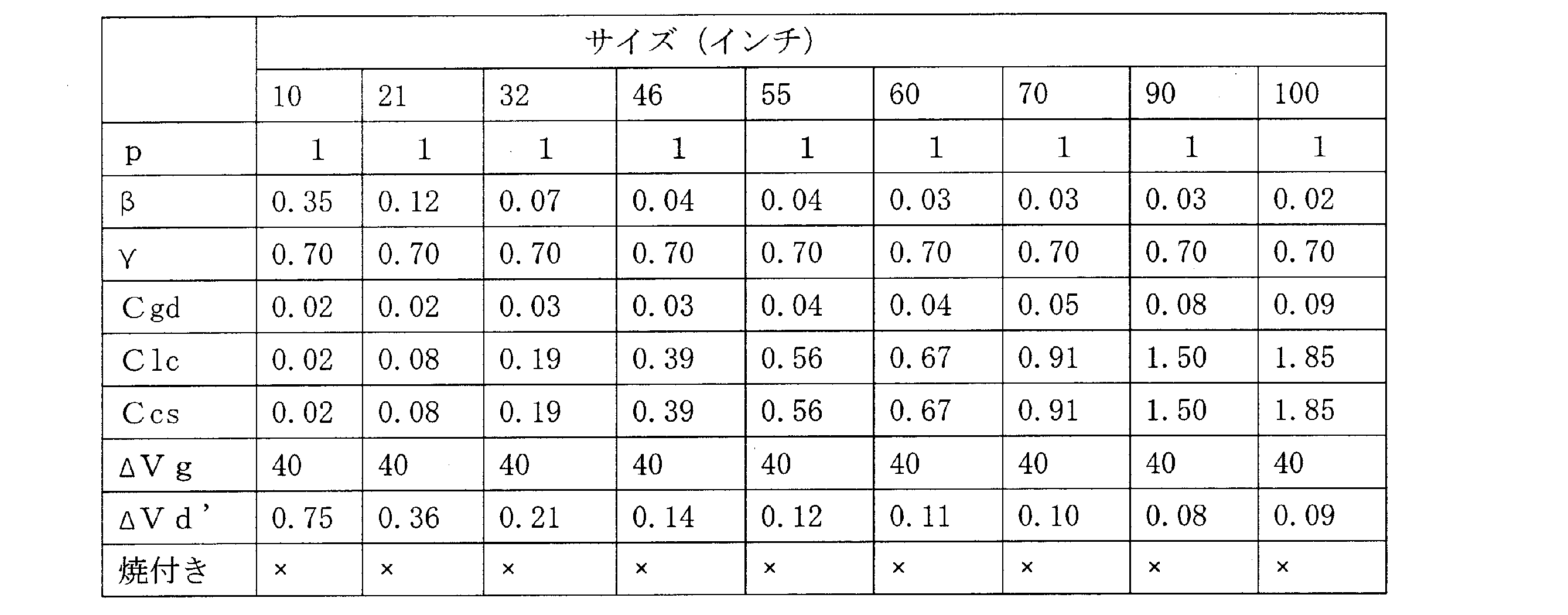
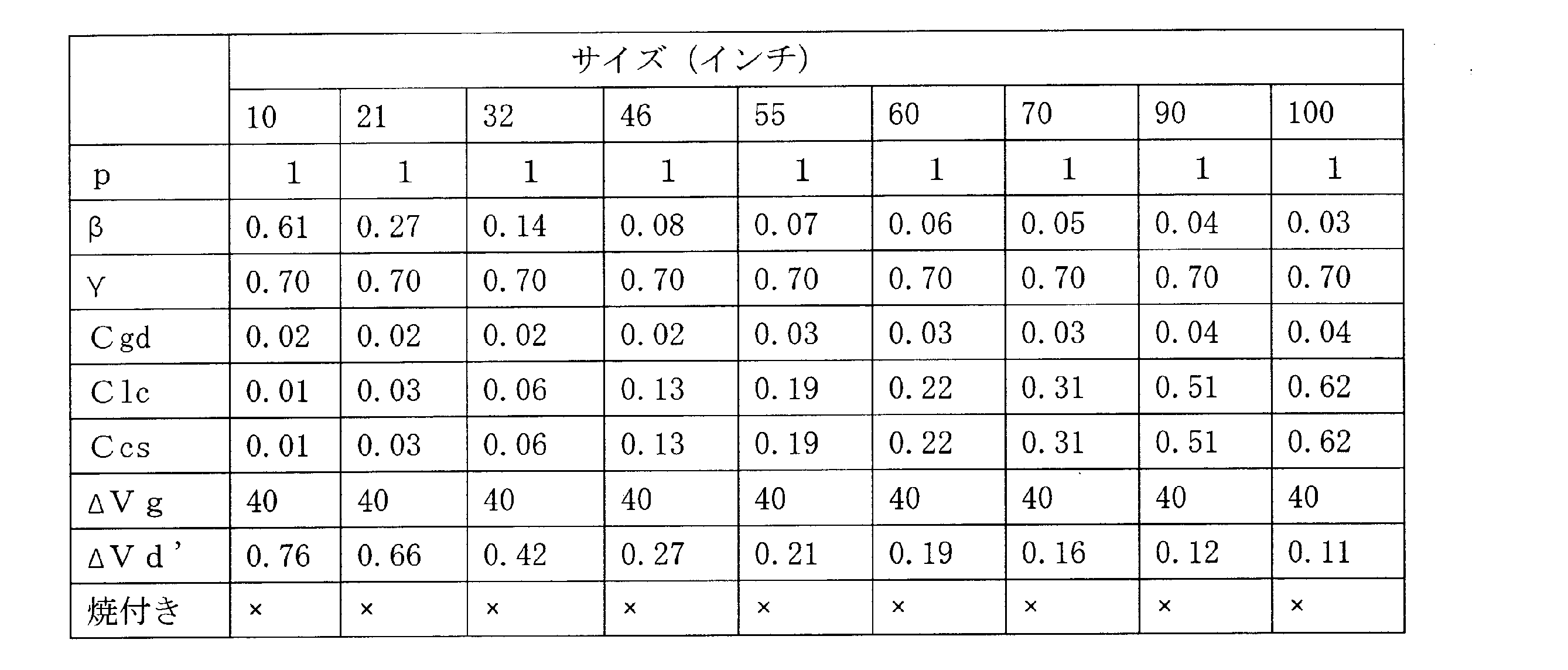
表4から明らかなように、第1の比較例では、有効表示領域Aでの画素数がFHDに対応したものである場合、有効表示領域Aのサイズに関わりなく、電圧ズレ量ΔVd'が全て0.04(V)を越える値となって焼付きが生じた。
同様に、表5から明らかなように、第1の比較例では、有効表示領域Aでの画素数がQXGAに対応したものである場合、有効表示領域Aのサイズに関わりなく、電圧ズレ量ΔVd'が全て0.04(V)を越える値となって焼付きが生じた。
同様に、表6から明らかなように、第1の比較例では、有効表示領域Aでの画素数がQFHDに対応したものである場合、有効表示領域Aのサイズに関わりなく、電圧ズレ量ΔVd'が全て0.04(V)を越える値となって焼付きが生じた。
つまり、本実施形態品では、第2の半導体層21bに酸化物半導体を用いているのに対して、第1の比較例では、第2の半導体層26b'にアモルファスシリコン層を用いるとともに、この第2の半導体層26b'の上面を覆うように、電極コンタクト層27'が形成されている。このため、第1の比較例では、液晶パネル2の使用に伴う(つまり、経年変化に伴う)、画素電極19'からドレイン電極24b'を介して電極コンタクト層27'及び第2の半導体層26b'への電圧印加に応じて、当該第2の半導体層26b'での閾値が変化して、補助容量部T4'の補助容量に変動が生じ、ひいては当該液晶パネル2に焼付きが生じる。
具体的にいえば、図19に示すように、曲線60及び61は、それぞれ上記閾値の変化前(初期値)及び変化後(画面を表示し続けたエージング後)における、第1の比較例での画素電圧-補助容量配線電圧と(補助)容量比との関係を示している。また、図19において、画素電圧-補助容量配線電圧の0よりも大きい値及び0よりも小さい値は、画素に対して、それぞれ上述の「+書き込み」及び「-書き込み」が行われたことに対応している。さらに、エージングの経過時間を増やしていけば、曲線61はさらに左にシフトすることとなる。
図19に示す通り、補助容量Ccsは、+書き込み、-書き込みによって変動し、具体的には、以下の(7)式及び(8)式にてそれぞれあらわされる。


但し、dGI及びεGIは、それぞれ第2のゲート絶縁膜20b’の膜厚及び誘電率である。また、di及びεiは、それぞれ第2の半導体層26b’の膜厚及び誘電率である。また、Sは、補助容量Ccsの面積である。
つまり、-書き込みの補助容量Ccs-は第2のゲート絶縁膜20b’のみで補助容量部を形成した場合に等しく、その値は+書き込みの補助容量より大きい。上記から第2のゲート絶縁膜20b’のみで補助容量部を形成した場合の共通電位(Vcom#g)、及び第2の半導体層26b’、電極コンタクト層27’により補助容量部を形成した場合の共通電位(Vcom#i)は、それぞれ下記の(9)式及び(10)式にてあらわされる。


上式より、補助容量部が第2の半導体層26b’、電極コンタクト層27’が存在せずに、第2のゲート絶縁膜20b’だけが補助容量配線CS’上に形成されている場合に比べて、共通電位Vcomは小さくなり、その分だけ小さく調整されて出荷される。
また、補助容量部T4’では、図19の曲線61に示すように、液晶パネル2の使用に伴い、第2の半導体層26b’での閾値が電極コンタクト層27’の存在により、例えば「-書き込み」側に変化する。この結果、補助容量部T4’では、後述するように、その補助容量が液晶パネル2の使用に伴って変化する。
尚、上記の説明以外に、第2の半導体層26b’のプロセス条件によっては、第2の半導体層26b’での閾値は+方向に変化する。
また、補助容量部T4’では、液晶パネル2の使用に伴い、第2の半導体層26b’での閾値が電極コンタクト層27’及び第2の半導体層26b’の存在により、「-書き込み」側に変化すると、補助容量が変化する。また、このように、補助容量部T4”の補助容量が変化するために、上記(4)式に示したように、引き込み電圧ΔVdが変わり、対向電圧(共通電位)Vcomもずれてくる。この結果、この第1の比較例では、電圧ズレ量ΔVd’が0.04(v)よりも大きくなり、焼付きが発生する。
次に、第2の比較例での試験結果の具体例について、説明する。
まず、図20を参照して、第2の比較例のアクティブマトリクス基板5"の補助容量部T4"の構成について説明する。
図20に示すように、この第2の比較例のアクティブマトリクス基板5”では、基材5a”上に補助容量配線CS”、ゲート絶縁膜20”、及び第2の半導体層26b”が順次形成されている。この第2の半導体層26b”は、例えばアモルファスシリコン層(i層)からなる半導体層26”によって構成されている。また、第2の半導体層26b”の右端部上には、例えばn+層からなる電極コンタクト層27”が設けられ、この電極コンタクト層27”にはドレイン電極(補助容量電極)24b”が接続されている。また、第2の比較例のアクティブマトリクス基板5”では、ゲート絶縁膜20”、第2の半導体層26b”、及びドレイン電極24b”を覆うように、保護層22”及び層間絶縁膜23”が順次形成されている。また、これらの保護層22”及び層間絶縁膜23”には、コンタクトホール部の開口部H2’が設けられており、この開口部H2’内で、画素電極19”とドレイン電極24b”が接続されている。
また、第2の比較例のアクティブマトリクス基板5”の補助容量部T4”では、その補助容量は補助容量配線CS”とその上方に順次設けられた第2のゲート絶縁膜20b”、第2の半導体層26b”、電極コンタクト層27”、及びドレイン電極24b”との間の部分と、補助容量配線CS”とその上方に順次設けられた第2のゲート絶縁膜20b”、及びドレイン電極24b” との間の部分とで生じるように構成されている。さらに、この補助容量部T4”は、本実施形態品と異なり、5枚のマスクを用いて、形成されている。
以下、第2の比較例での試験結果の具体例について、表7に示す。

表7から明らかなように、第2の比較例では、上記試作1及び試作2での電圧ズレ量ΔVd’が0.04(V)を越える値となって焼付きが生じた。一方、上記試作3~試作8では、電圧ズレ量ΔVd’が0.04(V)以下となって焼付きが生じなかった。
しかしながら、この第2の比較例は、上述したように、5枚のマスクを用いて形成されているので、4枚のマスクを用いて形成する本実施形態品に比べて、製造工程が複雑となり、また製造時間及び製造コストの低減を図るのが困難であるという問題点を生じる。また、この第2の比較例では、本実施形態品に比べて、液晶パネルの設計自由度が低いという問題点を生じる。
また、この第2の比較例では、第1の比較例と同様に、第2の半導体層26b”にアモルファスシリコン層を用いているので、本実施形態品に比べて、補助容量部T4”の容量変化が大きいものであった。具体的にいえば、図21に曲線71にて示すように、同図21の曲線70にて示す本実施形態品に比べて、容量変化が大きい。
一方、本実施形態品では、第2の半導体層26b’及び26b”にアモルファスシリコン層をそれぞれ用いた第1及び第2の比較例と異なり、第2の半導体層21bに酸化物半導体を用いている。このため、第2の半導体層21bでは、第2の半導体層26b’及び26b”のものに比べて、(電荷)移動度が大きい。具体的には、第2の半導体層21bでは、その移動度が5以上であるのに対して、第2の半導体層26b’及び26b”では、その移動度は0.3程度である。この結果、第2の半導体層26b’及び26b”の膜厚(例えば、2000~3000Å程度)に比べて、第2の半導体層21bの膜厚(例えば、200~800Å程度)を薄くすることができる。また、比誘電率は、アモルファスシリコン層が11程度に対し、酸化物半導体は15程度と大きい。これにより、本実施形態品では、第2の半導体層26b’及び26b”のものに比べて、上記γの値を大きくすることができる。すなわち、本実施形態品では、図16の曲線70に示したように、容量比γの値を0.95程度とでき、同図16の曲線71に示したように、第2の半導体層26b’及び26b”の容量比γの値、0.70程度よりも大きくできる。
また、本実施形態品では、第2の半導体層21bのオフ電流Ioffが第2の半導体層26b’及び26b”のものに比べて、小さいため、上記ΔVgの値を小さくできる。具体的には、第2の半導体層21bのオフ電流Ioffは1x10-12~1x10-14(A)程度であるのに対して、第2の半導体層26b’及び26b”のオフ電流Ioffは1x10⁻⁹~1x10-11(A)程度と大きい。このため、本実施形態品では、ΔVgを20~35(V)程度にできるのに対して、第1及び第2の比較例では、ΔVgを40(V)程度とする必要があった。この結果、本実施形態品では、表1~表3に例示したように、第1及び第2の比較例に比べて、電圧ズレ量ΔVd’を小さくすることができ、焼付きの発生を防止することができる。
以上のように構成された本実施形態の液晶パネル2では、薄膜トランジスタ部T1は基材5aとこの基材5a上に順次設けられたゲート電極18g、第1のゲート絶縁膜20a、第1の半導体層21a、ソース電極18s及びドレイン電極18d、保護層22、及び層間絶縁膜23を含んで構成されている。また、上記補助容量部T4は、基材5aとこの基材5a上に順次設けられた補助容量配線CS、第2のゲート絶縁膜20b、第2の半導体層21b、補助容量電極24b、及び画素電極(透明電極)19を含んで構成されている。これにより、本実施形態では、上記従来例と異なり、4枚のマスクを用いて、薄膜トランジスタ部T1と補助容量部T4を有するアクティブマトリクス基板5を適切に構成することができる。さらに、本実施形態の液晶パネル2では、酸化物半導体からなる第2の半導体層21bを用いるとともに、対向電極CEに生じる電圧ズレ量ΔVd’を、0.04(V)以下としている。これにより、本実施形態では、上記従来例と異なり、補助容量部T4の補助容量が変動した場合でも、焼付きが発生するのを防止できるコスト安価な液晶パネル2を提供することができる。
また、本実施形態では、ゲート電極18g及び補助容量配線CSには、基材5a上に形成された第1金属層FMが用いられている。これにより、本実施形態では、同一の第1金属層FMを用いて、ゲート電極18gと補助容量配線CSを構成することができ、より製造簡単でコスト安価な液晶パネル2を構成することができる。
また、本実施形態では、ソース電極18s、ドレイン電極18d、及び補助容量電極24bには、第1または第2の半導体層21a、21b上に形成された第2金属層24が用いられている。これにより、本実施形態では、同一の第2金属層24を用いて、ソース電極18s、ドレイン電極18d、及び補助容量電極24bを構成することができ、より製造簡単でコスト安価な液晶パネル2を構成することができる。
また、本実施形態では、第1及び第2のゲート絶縁膜20a、20bは、一体的に構成されている。これにより、本実施形態では、より製造簡単でコスト安価な液晶パネル2を構成することができる。
また、本実施形態では、補助容量部T4では、画素電極(透明電極)19は保護層22と層間絶縁膜23に設けられた開口部H2内で補助容量電極24bに接続されている。これにより、本実施形態では、より製造簡単でコスト安価な液晶パネル2を構成することができる。
また、上記の説明以外に、例えば図22に示すように、補助容量部T4において、各々1つの第2の半導体層21b、補助容量電極24b、及び開口部H2を幅太部CS2上に設ける構成でもよい。
[第2の実施形態]
図23は、本発明の第2の実施形態に係る液晶パネルのアクティブマトリクス基板の要部構成を説明する拡大平面図である。図24は、図23に示したアクティブマトリクス基板の補助容量部を示す断面図である。
図23は、本発明の第2の実施形態に係る液晶パネルのアクティブマトリクス基板の要部構成を説明する拡大平面図である。図24は、図23に示したアクティブマトリクス基板の補助容量部を示す断面図である。
図において、本実施形態と上記第1の実施形態との主な相違点は、第1及び第2の半導体層を一体的に構成するとともに、ドレイン電極と補助容量電極とを一体的に構成した点である。なお、上記第1の実施形態と共通する要素については、同じ符号を付して、その重複した説明を省略する。
つまり、図23及び図24に示すように、本実施形態のアクティブマトリクス基板5では、上記第2工程の際に、ドレイン電極18dと補助容量電極24bとが、一体的に構成される。また、当該第2工程の際に、一体的に構成されたドレイン電極18dと補助容量電極24bとの下方において、第1及び第2の半導体層21a、21bが一体的に構成される。すなわち、本実施形態のアクティブマトリクス基板5では、薄膜トランジスタ部T1、画素コンタクト部T2、及び補助容量部T4だけでなく、画素部T3の一部分にも、一体的に構成された第1及び第2の半導体層21a、21bと、一体的に構成されたドレイン電極18dと補助容量電極24bが含まれる。
以上の構成により、本実施形態では、上記第1の実施形態と同様な作用・効果を奏することができる。また、本実施形態では、第1及び第2の半導体層21a、21bが、一体的に構成されているとともに、ドレイン電極18dと補助容量電極24bとが、一体的に構成されている。これにより、本実施形態では、コンタクトホール部の開口部の設置数を削減することができ、コスト安価な液晶パネル2を容易に構成することができる。また、補助容量部T4の2つの補助容量電極24bの各々に対して、一体的に構成したドレイン電極18dで導通しているので、片方の補助容量電極24bが補助容量配線CSとの間に異物が発生してリークしたとしても、そのリークした方の補助容量電極24bと一体的に構成したドレイン電極18dをレーザーカットすることにより、正常点灯させ、歩留まりを上げることができる。
また、上記の説明以外に、例えば図25に示すように、補助容量部T4において、各々1つの第2の半導体層21b、補助容量電極24b、及び開口部H2を幅太部CS2上に設ける構成でもよい。
[第3の実施形態]
図26は、本発明の第3の実施形態に係る液晶パネルのアクティブマトリクス基板の要部構成を説明する拡大平面図である。図27は、図26に示したアクティブマトリクス基板の補助容量部を示す断面図である。
図26は、本発明の第3の実施形態に係る液晶パネルのアクティブマトリクス基板の要部構成を説明する拡大平面図である。図27は、図26に示したアクティブマトリクス基板の補助容量部を示す断面図である。
図において、本実施形態と上記第1の実施形態との主な相違点は、補助容量部において、補助容量配線の対向する部分よりも大きくなるように、補助容量電極を設けた点である。なお、上記第1の実施形態と共通する要素については、同じ符号を付して、その重複した説明を省略する。
つまり、図26及び図27に示すように、本実施形態のアクティブマトリクス基板5の補助容量配線CSでは、上記第1工程の際に、スリットCS3が幅太部CS2の幅方向(図26の上下方向)の中央部に形成される。また、補助容量部T4では、幅太部CS2上に、第2のゲート絶縁膜20b、第2の半導体層21b、補助容量電極24b、及び画素電極(透明電極)19が順次設けられている。
また、補助容量部T4では、補助容量電極24bは補助容量配線CSの対向する部分よりも大きくなるように、設けられている。
以上の構成により、本実施形態では、上記第1の実施形態と同様な作用・効果を奏することができる。また、本実施形態では、補助容量部T4において、補助容量電極24bが補助容量配線CSの対向する部分よりも大きく設けられている。これにより、本実施形態では、補助容量部T4において、補助容量配線CSの対向面積を確実に補助容量の発生部分として利用することができ、補助容量部T4の補助容量の低下を確実に防止することができる。
また、本実施形態では、スリットCS3を設けることにより、第3工程の精度よりも第1工程の精度の方がよい場合、補助容量Ccsのばらつきが第1工程のプロセス精度で決まることにより、補助容量Ccsのばらつきを小さくすることができる。つまり、開口部H2が設けられる保護層22及び層間絶縁膜23の各製造バラツキの影響が補助容量部T4に現れるのを確実に防ぐことができ、補助容量部T4を高精度に形成して、補助容量部T4の補助容量Ccsの低下を確実に防止することができる。
また、上記の説明以外に、例えば図28に示すように、補助容量部T4において、各々1つの第2の半導体層21b、補助容量電極24b、及び開口部H2を幅太部CS2上に設ける構成でもよい。
[第4の実施形態]
図29は、本発明の第4の実施形態に係る液晶パネルのアクティブマトリクス基板の要部構成を説明する拡大平面図である。図30は、図29に示したアクティブマトリクス基板の補助容量部を示す断面図である。
図29は、本発明の第4の実施形態に係る液晶パネルのアクティブマトリクス基板の要部構成を説明する拡大平面図である。図30は、図29に示したアクティブマトリクス基板の補助容量部を示す断面図である。
図において、本実施形態と上記第1の実施形態との主な相違点は、薄膜トランジスタ部側に分岐した分岐配線を補助容量配線に設けるとともに、当該分岐配線上に、第2のゲート絶縁膜、第2の半導体層、補助容量電極、及び第2の透明電極を順次設けた点である。なお、上記第1の実施形態と共通する要素については、同じ符号を付して、その重複した説明を省略する。
つまり、図29及び図30に示すように、本実施形態のアクティブマトリクス基板5の補助容量配線CSでは、上記第1工程の際に、複数、例えば2本の分岐配線CS4が設けられている。これらの各分岐配線CS4は、図29に示すように、薄膜トランジスタ部T1側に分岐するよう設けられている。
また、本実施形態のアクティブマトリクス基板5では、2つの補助容量部T4が、2本の分岐配線CS4にそれぞれ応じて、形成されている。つまり、各補助容量部T4では、分岐配線CS4上に、第2のゲート絶縁膜20b、第2の半導体層21b、補助容量電極24b、及び画素電極(透明電極)19が順次設けられている。また、画素電極19は、開口部H2aの内部で補助容量電極24bに接続されている。
以上の構成により、本実施形態では、上記第1の実施形態と同様な作用・効果を奏することができる。また、本実施形態では、補助容量配線CSに2本の分岐配線CS4を設けることにより、2つの補助容量部T4の合計の補助容量(つまり、画素単位の補助容量)を容易に大きくすることができる。また、片方の補助容量部T4が補助容量配線CSの分岐配線CS4と補助容量電極24bの間に異物が発生しリークしたとしても、そのリークした方の補助容量配線CSの分岐配線CS4をレーザーカットすることにより、正常点灯させ、歩留まりを上げることができる。また、第3工程の精度よりも第1工程の精度の方がよい場合、補助容量Ccsのばらつきが第1工程のプロセス精度で決まることにより、補助容量Ccsのばらつきを小さくすることができる。つまり、開口部H2aが設けられる保護層22及び層間絶縁膜23の各製造バラツキの影響が補助容量部T4に現れるのを確実に防ぐことができ、補助容量部T4を高精度に形成して、補助容量部T4の補助容量Ccsの低下を確実に防止することができる。また、第3工程の精度の方がよい場合、補助容量電極24bがすべての分岐配線CS4を覆う構成でなく、一方の長辺の分岐配線CS4のみを覆う構成としてもよい。
尚、上記の実施形態はすべて例示であって制限的なものではない。本発明の技術的範囲は特許請求の範囲によって規定され、そこに記載された構成と均等の範囲内のすべての変更も本発明の技術的範囲に含まれる。
例えば、保護層、層間絶縁膜は1層に限られるわけはなく、それぞれ2層以上であってもよい。また、画素電極の上に絶縁膜がさらに構成される形状であってもよい。さらに、上記の説明では、本発明を透過型の液晶表示装置に適用した場合について説明したが、本発明の液晶パネルはこれに限定されるものではなく、半透過型や反射型の液晶表示装置に適用することができる。
また、上記の説明では、補助容量用配線をソースドライバ(駆動部)に接続した構成について説明したが、本発明はこれに限定されるものではなく、例えば駆動部としてのゲートドライバに補助容量用配線を接続したり、補助容量用配線専用の駆動部(ドライバ)に接続したりして、補助容量を発生させる構成でもよい。
また、上記の説明以外に、例えば図31に示すように、ゲート配線Gを上下の画素Pで共通となるように構成してもよい。この構成により、上下それぞれが副画素となり、2つで1つの画素を構成し、例えば上画素が明画素、下画素が暗画素とすることにより、視野角を向上させることができる。この場合、補助容量配線CSの電位は上下の画素で異なる電位が入力される。例えば、画素電極19に対し、+の書き込みがされた場合には、上の副画素に対応する補助容量配線CSは1V、下の副画素に対応する補助容量配線CSは-1Vの電位となる。補助容量により、上の副画素は書き込みされた電位よりも大きくなり、下の副画素は書き込みされた電位よりも小さくなる。このように、視野角を向上させることができる。
また、上記の説明以外に、薄膜トランジスタ部において、複数の薄膜トランジスタを設ける構成でもよい。
また、上記の説明以外に、上記第1~第4の各実施形態を適宜組み合わせたものでもよい。
本発明は、マスク枚数を低減することができるとともに、焼付きの発生を防止することができるコスト安価な液晶パネル、及びその製造方法に対して有用である。
2 液晶パネル
4 カラーフィルタ基板(対向基板)
5 アクティブマトリクス基板
5a 基材
18 薄膜トランジスタ
18g ゲート電極(第1金属層)
18s ソース電極(第2金属層)
18d ドレイン電極(第2金属層)
19 画素電極(透明電極)
20 ゲート絶縁膜
20a 第1のゲート絶縁膜
20b 第2のゲート絶縁膜
21 半導体層
21a 第1の半導体層
21b 第2の半導体層
22 保護層
23 層間絶縁膜
24 第2金属層
24b 補助容量電極
P 画素
A 有効表示領域
CE 対向電極
LC 液晶層
T1 薄膜トランジスタ部
T4 補助容量部
CS 補助容量配線
CS3 スリット
CS4 分岐配線
FM 第1金属層
H2、H2a 開口部
M1 第1のマスク
M2 第2のマスク(ハーフトーンマスク)
M3 第3のマスク
M4 第4のマスク
4 カラーフィルタ基板(対向基板)
5 アクティブマトリクス基板
5a 基材
18 薄膜トランジスタ
18g ゲート電極(第1金属層)
18s ソース電極(第2金属層)
18d ドレイン電極(第2金属層)
19 画素電極(透明電極)
20 ゲート絶縁膜
20a 第1のゲート絶縁膜
20b 第2のゲート絶縁膜
21 半導体層
21a 第1の半導体層
21b 第2の半導体層
22 保護層
23 層間絶縁膜
24 第2金属層
24b 補助容量電極
P 画素
A 有効表示領域
CE 対向電極
LC 液晶層
T1 薄膜トランジスタ部
T4 補助容量部
CS 補助容量配線
CS3 スリット
CS4 分岐配線
FM 第1金属層
H2、H2a 開口部
M1 第1のマスク
M2 第2のマスク(ハーフトーンマスク)
M3 第3のマスク
M4 第4のマスク
Claims (15)
- 複数の画素が設けられるとともに、前記複数の画素毎に薄膜トランジスタが形成された薄膜トランジスタ部及び補助容量を発生する補助容量部が設けられたアクティブマトリクス基板と、対向電極が設けられた対向基板と、前記アクティブマトリクス基板と前記対向基板との間に設けられた液晶層とを有する液晶パネルであって、
前記薄膜トランジスタ部は、基材と、前記基材上に設けられたゲート電極と、前記基材及び前記ゲート電極を覆うように設けられた第1のゲート絶縁膜と、前記第1のゲート絶縁膜上に設けられるとともに、酸化物半導体からなる第1の半導体層と、前記第1の半導体層上に設けられて当該第1の半導体層に接続されたソース電極と、前記第1の半導体層上に設けられて当該第1の半導体層に接続されたドレイン電極と、前記第1のゲート絶縁膜、前記第1の半導体層、前記ソース電極、及び前記ドレイン電極を覆うように設けられた保護層と、前記保護層上に設けられた層間絶縁膜を含んで構成され、
前記補助容量部は、前記基材と、前記基材上に設けられた補助容量配線と、前記基材及び前記補助容量配線を覆うように設けられた第2のゲート絶縁膜と、前記第2のゲート絶縁膜上に設けられるとともに、酸化物半導体からなる第2の半導体層と、前記第2の半導体層上に設けられて当該第2の半導体層に接続された補助容量電極と、前記補助容量電極に接続された透明電極とを含んで構成され、
前記補助容量部の面積での前記第2の半導体層の面積の割合をpとし、前記ゲート電極と前記ドレイン電極との間の静電容量をCgdとし、前記液晶層の静電容量をClcとし、前記補助容量部の補助容量をCcsとし、Cgd/(Cgd+Clc+Ccs)の値をβとし、前記補助容量部の補助容量に対する前記第2のゲート絶縁膜による補助容量の比をγとし、前記ゲート電極へのオン電圧とオフ電圧との電圧差をΔVgとしたときに、

ことを特徴とする液晶パネル。 - 前記ゲート電極及び前記補助容量配線には、前記基材上に形成された第1金属層が用いられている請求項1に記載の液晶パネル。
- 前記ソース電極、前記ドレイン電極、及び前記補助容量電極には、前記第1または第2の半導体層上に形成された第2金属層が用いられている請求項1または2に記載の液晶パネル。
- 前記補助容量部では、前記透明電極は前記保護層と前記層間絶縁膜に設けられた開口部内で前記補助容量電極に接続されている請求項1~3のいずれか1項に記載の液晶パネル。
- 前記第1及び第2の半導体層が、一体的に構成されているとともに、
前記ドレイン電極と前記補助容量電極とが、一体的に構成されている請求項1~4のいずれか1項に記載の液晶パネル。 - 前記補助容量部では、前記補助容量電極が前記補助容量配線の対向する部分よりも大きく設けられている請求項1~5のいずれか1項に記載の液晶パネル。
- 前記補助容量部では、前記補助容量配線にスリットが設けられている請求項1~6のいずれか1項に記載の液晶パネル。
- 前記補助容量配線には、前記薄膜トランジスタ部側に分岐した分岐配線が設けられ、
前記補助容量部では、前記分岐配線上に、前記第2のゲート絶縁膜、前記第2の半導体層、前記補助容量電極、及び前記透明電極が順次設けられている請求項1~7のいずれか1項に記載の液晶パネル。 - 前記複数の画素を含んだ有効表示領域を有するとともに、
前記有効表示領域での画素数が、FHD(Full High Definition)に対応したものである場合、当該有効表示領域は、21インチ以上に構成されている請求項1~8のいずれか1項に記載の液晶パネル。 - 前記複数の画素を含んだ有効表示領域を有するとともに、
前記有効表示領域での画素数が、QXGA(Quad eXtended Graphics Array)に対応したものである場合、当該有効表示領域は、21インチ以上に構成されている請求項1~8のいずれか1項に記載の液晶パネル。 - 前記複数の画素を含んだ有効表示領域を有するとともに、
前記有効表示領域での画素数が、QFHD(Quad Full High Definition)に対応したものである場合、当該有効表示領域は、46インチ以上に構成されている請求項1~8のいずれか1項に記載の液晶パネル。 - 複数の画素が設けられるとともに、前記複数の画素毎に薄膜トランジスタが形成された薄膜トランジスタ部及び補助容量を発生する補助容量部が設けられたアクティブマトリクス基板と、対向電極が設けられた対向基板と、前記アクティブマトリクス基板と前記対向基板との間に設けられた液晶層とを有する液晶パネルの製造方法であって、
前記アクティブマトリクス基板の製造工程は、
第1金属層を基材上に形成した後、当該第1金属層に対して、第1のマスクを用いてパターニングを行うことにより、前記薄膜トランジスタ部のゲート電極及び前記補助容量部の補助容量配線を形成する第1工程と、
ゲート絶縁膜、酸化物半導体からなる半導体層、及び第2金属層を順次形成した後、ハーフトーンマスクからなる第2のマスクを用いてパターニングを行うことにより、前記薄膜トランジスタ部の第 1の半導体層とソース電極とドレイン電極及び前記補助容量部の第2の半導体層と補助容量電極を形成する第2工程と、
保護層及び層間絶縁膜を順次形成した後、第3のマスクを用いてパターニングを行うことにより、開口部を前記保護層と前記層間絶縁膜に形成する第3工程と、
透明電極を形成した後、第4のマスクを用いてパターニングを行うことにより、前記補助容量部の透明電極を形成する第4工程とを具備し、かつ、
前記補助容量部の面積での前記第2の半導体層の面積の割合をpとし、前記ゲート電極と前記ドレイン電極との間の静電容量をCgdとし、前記液晶層の静電容量をClcとし、前記補助容量部の補助容量をCcsとし、Cgd/(Cgd+Clc+Ccs)の値をβとし、前記補助容量部の補助容量に対する前記第2のゲート絶縁膜による補助容量の比をγとし、前記ゲート電極へのオン電圧とオフ電圧との電圧差をΔVgとしたときに、

ことを特徴とする液晶パネルの製造方法。 - 前記第2工程では、前記第1及び第2の半導体層を一体的に形成するとともに、前記ドレイン電極と前記補助容量電極を一体的に形成する請求項12に記載の液晶パネルの製造方法。
- 前記第2工程では、前記補助容量電極が前記補助容量配線の対向する部分よりも大きくなるように形成される請求項12または13に記載の液晶パネルの製造方法。
- 前記第1工程では、前記補助容量部の補助容量配線において、スリットが形成される請求項12~14のいずれか1項に記載の液晶パネルの製造方法。
Applications Claiming Priority (2)
| Application Number | Priority Date | Filing Date | Title |
|---|---|---|---|
| JP2012-220145 | 2012-10-02 | ||
| JP2012220145 | 2012-10-02 |
Publications (1)
| Publication Number | Publication Date |
|---|---|
| WO2014054487A1 true WO2014054487A1 (ja) | 2014-04-10 |
Family
ID=50434815
Family Applications (1)
| Application Number | Title | Priority Date | Filing Date |
|---|---|---|---|
| PCT/JP2013/075900 Ceased WO2014054487A1 (ja) | 2012-10-02 | 2013-09-25 | 液晶パネル、及び製造方法 |
Country Status (1)
| Country | Link |
|---|---|
| WO (1) | WO2014054487A1 (ja) |
Citations (5)
| Publication number | Priority date | Publication date | Assignee | Title |
|---|---|---|---|---|
| JPH09325356A (ja) * | 1996-06-03 | 1997-12-16 | Sharp Corp | アクティブマトリクス基板 |
| JP2000214481A (ja) * | 1999-01-22 | 2000-08-04 | Advanced Display Inc | 液晶表示装置およびその製造方法 |
| JP2004361930A (ja) * | 2003-05-15 | 2004-12-24 | Sharp Corp | 液晶表示装置およびその駆動方法 |
| JP2007027735A (ja) * | 2005-07-12 | 2007-02-01 | Samsung Electronics Co Ltd | 薄膜トランジスタ表示板及びその製造方法 |
| JP2008309831A (ja) * | 2007-06-12 | 2008-12-25 | Epson Imaging Devices Corp | 液晶表示パネル及びその製造方法 |
-
2013
- 2013-09-25 WO PCT/JP2013/075900 patent/WO2014054487A1/ja not_active Ceased
Patent Citations (5)
| Publication number | Priority date | Publication date | Assignee | Title |
|---|---|---|---|---|
| JPH09325356A (ja) * | 1996-06-03 | 1997-12-16 | Sharp Corp | アクティブマトリクス基板 |
| JP2000214481A (ja) * | 1999-01-22 | 2000-08-04 | Advanced Display Inc | 液晶表示装置およびその製造方法 |
| JP2004361930A (ja) * | 2003-05-15 | 2004-12-24 | Sharp Corp | 液晶表示装置およびその駆動方法 |
| JP2007027735A (ja) * | 2005-07-12 | 2007-02-01 | Samsung Electronics Co Ltd | 薄膜トランジスタ表示板及びその製造方法 |
| JP2008309831A (ja) * | 2007-06-12 | 2008-12-25 | Epson Imaging Devices Corp | 液晶表示パネル及びその製造方法 |
Similar Documents
| Publication | Publication Date | Title |
|---|---|---|
| JP4583922B2 (ja) | 液晶表示装置及びその製造方法 | |
| US8149228B2 (en) | Active matrix substrate | |
| JPH09113931A (ja) | 液晶表示装置 | |
| EP2991121B1 (en) | Array substrate, method for manufacturing array substrate and display device | |
| US20250389994A1 (en) | Array substrate, manufacturing method thereof, and display panel | |
| US9110327B2 (en) | Trans-reflective liquid crystal display array substrate, manufacturing method thereof and display device | |
| US9971212B2 (en) | Array substrate, liquid crystal display panel, and liquid crystal display | |
| US7868955B2 (en) | Liquid crystal display and method for manufacturing the same | |
| KR20160053261A (ko) | 박막 트랜지스터 기판 및 이의 제조 방법 | |
| US9235091B2 (en) | Liquid crystal display device and manufacturing method thereof | |
| WO2011074336A1 (ja) | アクティブマトリクス基板、及び製造方法 | |
| CN207337004U (zh) | 液晶显示装置 | |
| WO2010103676A1 (ja) | アクティブマトリクス基板、表示パネル、表示装置、並びに電子機器 | |
| US10067393B2 (en) | Thin film display panel and liquid crystal display device including the same | |
| US9134565B2 (en) | Pixel unit and display panel having the same | |
| JP5185447B2 (ja) | アクティブマトリクス基板、製造方法、及び表示装置 | |
| US10209541B2 (en) | Liquid crystal display device and method for manufacturing the same | |
| US20050088582A1 (en) | Liquid crystal display | |
| US20130102115A1 (en) | Method for manufacturing active matrix substrate | |
| US9490269B2 (en) | Display device | |
| WO2014054487A1 (ja) | 液晶パネル、及び製造方法 | |
| TW202205067A (zh) | 內嵌式觸控顯示面板 | |
| JP2013250319A (ja) | アクティブマトリクス基板、製造方法、及び表示装置 | |
| JP6503052B2 (ja) | 液晶表示装置 | |
| US10964251B2 (en) | Pixel array substrate and driving method thereof |
Legal Events
| Date | Code | Title | Description |
|---|---|---|---|
| 121 | Ep: the epo has been informed by wipo that ep was designated in this application |
Ref document number: 13843922 Country of ref document: EP Kind code of ref document: A1 |
|
| NENP | Non-entry into the national phase |
Ref country code: DE |
|
| 122 | Ep: pct application non-entry in european phase |
Ref document number: 13843922 Country of ref document: EP Kind code of ref document: A1 |
|
| NENP | Non-entry into the national phase |
Ref country code: JP |