WO2014050834A1 - オルガノポリシロキサン、オルガノポリシロキサンの製造方法、架橋オルガノポリシロキサン、およびコーティング用組成物 - Google Patents
オルガノポリシロキサン、オルガノポリシロキサンの製造方法、架橋オルガノポリシロキサン、およびコーティング用組成物 Download PDFInfo
- Publication number
- WO2014050834A1 WO2014050834A1 PCT/JP2013/075766 JP2013075766W WO2014050834A1 WO 2014050834 A1 WO2014050834 A1 WO 2014050834A1 JP 2013075766 W JP2013075766 W JP 2013075766W WO 2014050834 A1 WO2014050834 A1 WO 2014050834A1
- Authority
- WO
- WIPO (PCT)
- Prior art keywords
- organopolysiloxane
- glass substrate
- siloxane unit
- formula
- group
- Prior art date
- Legal status (The legal status is an assumption and is not a legal conclusion. Google has not performed a legal analysis and makes no representation as to the accuracy of the status listed.)
- Ceased
Links
- 0 CN(C)[Si](*)(*)N(C)C Chemical compound CN(C)[Si](*)(*)N(C)C 0.000 description 1
Images


Classifications
-
- C—CHEMISTRY; METALLURGY
- C08—ORGANIC MACROMOLECULAR COMPOUNDS; THEIR PREPARATION OR CHEMICAL WORKING-UP; COMPOSITIONS BASED THEREON
- C08G—MACROMOLECULAR COMPOUNDS OBTAINED OTHERWISE THAN BY REACTIONS ONLY INVOLVING UNSATURATED CARBON-TO-CARBON BONDS
- C08G77/00—Macromolecular compounds obtained by reactions forming a linkage containing silicon with or without sulfur, nitrogen, oxygen or carbon in the main chain of the macromolecule
- C08G77/48—Macromolecular compounds obtained by reactions forming a linkage containing silicon with or without sulfur, nitrogen, oxygen or carbon in the main chain of the macromolecule in which at least two but not all the silicon atoms are connected by linkages other than oxygen atoms
- C08G77/50—Macromolecular compounds obtained by reactions forming a linkage containing silicon with or without sulfur, nitrogen, oxygen or carbon in the main chain of the macromolecule in which at least two but not all the silicon atoms are connected by linkages other than oxygen atoms by carbon linkages
- C08G77/52—Macromolecular compounds obtained by reactions forming a linkage containing silicon with or without sulfur, nitrogen, oxygen or carbon in the main chain of the macromolecule in which at least two but not all the silicon atoms are connected by linkages other than oxygen atoms by carbon linkages containing aromatic rings
-
- C—CHEMISTRY; METALLURGY
- C09—DYES; PAINTS; POLISHES; NATURAL RESINS; ADHESIVES; COMPOSITIONS NOT OTHERWISE PROVIDED FOR; APPLICATIONS OF MATERIALS NOT OTHERWISE PROVIDED FOR
- C09D—COATING COMPOSITIONS, e.g. PAINTS, VARNISHES OR LACQUERS; FILLING PASTES; CHEMICAL PAINT OR INK REMOVERS; INKS; CORRECTING FLUIDS; WOODSTAINS; PASTES OR SOLIDS FOR COLOURING OR PRINTING; USE OF MATERIALS THEREFOR
- C09D183/00—Coating compositions based on macromolecular compounds obtained by reactions forming in the main chain of the macromolecule a linkage containing silicon, with or without sulfur, nitrogen, oxygen, or carbon only; Coating compositions based on derivatives of such polymers
- C09D183/14—Coating compositions based on macromolecular compounds obtained by reactions forming in the main chain of the macromolecule a linkage containing silicon, with or without sulfur, nitrogen, oxygen, or carbon only; Coating compositions based on derivatives of such polymers in which at least two but not all the silicon atoms are connected by linkages other than oxygen atoms
-
- Y—GENERAL TAGGING OF NEW TECHNOLOGICAL DEVELOPMENTS; GENERAL TAGGING OF CROSS-SECTIONAL TECHNOLOGIES SPANNING OVER SEVERAL SECTIONS OF THE IPC; TECHNICAL SUBJECTS COVERED BY FORMER USPC CROSS-REFERENCE ART COLLECTIONS [XRACs] AND DIGESTS
- Y02—TECHNOLOGIES OR APPLICATIONS FOR MITIGATION OR ADAPTATION AGAINST CLIMATE CHANGE
- Y02P—CLIMATE CHANGE MITIGATION TECHNOLOGIES IN THE PRODUCTION OR PROCESSING OF GOODS
- Y02P20/00—Technologies relating to chemical industry
- Y02P20/50—Improvements relating to the production of bulk chemicals
- Y02P20/582—Recycling of unreacted starting or intermediate materials
Definitions
- the present invention relates to an organopolysiloxane, a method for producing organopolysiloxane, a crosslinked organopolysiloxane that is a crosslinked product of organopolysiloxane, and a coating composition containing the organopolysiloxane.
- devices such as solar cells (PV), liquid crystal panels (LCD), and organic EL panels (OLED) have been made thinner and lighter, and the glass substrates used in these devices have been made thinner. Progressing. If the strength of the glass substrate is insufficient due to the thinning, the handling property of the glass substrate is lowered in the device manufacturing process.
- PV solar cells
- LCD liquid crystal panels
- OLED organic EL panels
- a method of forming a device member for example, a thin film transistor
- a glass substrate thicker than the final thickness and then thinning the glass substrate by chemical etching is widely used.
- this method for example, when the thickness of one glass substrate is reduced from 0.7 mm to 0.2 mm or 0.1 mm, most of the original glass substrate material is scraped off with an etching solution. Therefore, it is not preferable from the viewpoint of productivity and use efficiency of raw materials.
- the method of thinning a glass substrate by the above chemical etching if a fine scratch exists on the surface of the glass substrate, a fine recess (etch pit) is formed from the scratch by the etching process, resulting in an optical defect. There was a case.
- the reinforcing plate has a support plate and a silicone resin layer made of a crosslinked organopolysiloxane fixed on the support plate, and the silicone resin layer and the thin glass substrate are in close contact with each other so as to be peeled off.
- the interface between the silicone resin layer of the glass laminate and the thin glass substrate is peeled off, and the reinforcing plate separated from the thin glass substrate is laminated with a new thin glass substrate and can be reused as a glass laminate.
- the present invention has been made in view of the above points.
- the present invention adheres detachably to a laminated glass substrate and suppresses decomposition under high-temperature treatment conditions.
- An object is to provide an organopolysiloxane.
- the inventors of the present invention have a crosslinked organopolysiloxane having a specific structure, while exhibiting good adhesion to the laminated glass substrate,
- the present invention has been completed by finding that it can be easily peeled off and further that decomposition under high temperature treatment conditions is suppressed. That is, the present invention provides the following (i) to (x).
- siloxane units is an alkyl group (B-1), and none of R 5 and R 6 consists of siloxane units is an alkyl group having 4 or less carbon atoms, respectively (B-2),
- the ratio of [siloxane unit (B-1)] ⁇ 100 / [siloxane unit (B-1) + siloxane unit (B-2)], which is the ratio of the siloxane unit (B-1) to the siloxane unit (B), is 25.
- Organopolysiloxane which is ⁇ 90 mol%.
- R 1 to R 4 each independently represents an alkyl group having 4 or less carbon atoms
- Ar represents a phenylene group which may have a substituent.
- R 5 and R 6 each independently represents an alkyl group having 4 or less carbon atoms or an alkenyl group having 3 or less carbon atoms.
- the silane compound represented is a silane compound in which at least one of R 5 and R 6 is an alkenyl group having 3 or less carbon atoms, and R 5 and R 6 other than the alkenyl group are alkyl groups having 4 or less carbon atoms, and , Each of R 5 and R 6 is composed of a silane compound that is an alkyl group having 4 or less carbon atoms.
- R 1 ⁇ R 4 and Ar have the same meanings as R 1 ⁇ R 4 and Ar in Formula (1), in the formula (4), R 5 and R 6 has the formula (2) It is synonymous with R 5 and R 6 in the formula, and in formula (3) and formula (4), X and Y each independently represent a hydrogen atom, a hydroxy group or a hydrolyzable group.
- (Viii) A crosslinked organopolysiloxane, which is a crosslinked product obtained by crosslinking the organopolysiloxane according to any one of (i) to (vi) above.
- (Ix) The crosslinked organopolysiloxane according to (viii) above, wherein the crosslinking is thermal crosslinking.
- (X) A coating composition comprising the organopolysiloxane according to any one of (i) to (vi) above and a solvent.
- an organopolysiloxane that, when a crosslinked product is used, has adhesion to a laminated glass substrate and suppresses decomposition under high-temperature treatment conditions.
- FIG. 1 is a schematic cross-sectional view showing an embodiment of a glass laminate.
- 2A to 2D are schematic cross-sectional views showing an embodiment of a method for producing a glass substrate with members in the order of steps.
- organopolysiloxane In describing the organopolysiloxane of the present invention, first, general organopolysiloxane will be described. Usually, the basic structural unit of organopolysiloxane is classified according to how many monovalent organic groups represented by methyl group and phenyl group are bonded to a silicon atom, and is called D unit as shown below. Bifunctional siloxane unit with two organic groups bonded, called T unit, trifunctional siloxane unit with one organic group bonded, monofunctional siloxane called M unit with three organic groups bonded It consists of a unit and a tetrafunctional siloxane unit called Q unit which has no organic group.
- the Q unit is a unit that does not have an organic group bonded to a silicon atom (an organic group having a carbon atom bonded to a silicon atom), but is regarded as a siloxane unit in the present invention.
- R represents a monovalent organic group represented by a methyl group or a phenyl group.
- the siloxane bond is a bond in which two silicon atoms are bonded through one oxygen atom, so that the oxygen atom per silicon atom in the siloxane bond is regarded as 1 ⁇ 2, O 1/2 is expressed.
- one silicon atom is bonded to two oxygen atoms, and each oxygen atom is bonded to a silicon atom of another unit.
- the formula is -O 1/2 -R 2 Si-O 1/ 2- . Since there are two O 1/2 s , the D unit is usually expressed as R 2 SiO 2/2 .
- an O 1/2 expression is used for each oxygen atom to express the M unit, the D unit, the T unit, and the Q unit as follows.
- the atoms other than the silicon atom bonded to the O 1/2 of the terminal unit are 1 ⁇ 2 oxygen atoms, and one in total And represents an oxygen atom in a hydroxyl group or an alkoxy group.
- the hydroxyl group bonded to the silicon atom of the terminal unit is —O 1/2 —H.
- the organopolysiloxane of the present invention is roughly an organopolysiloxane containing a siloxane unit (A) represented by the formula (1) and a siloxane unit (B) represented by the formula (2).
- a siloxane unit (A) represented by the formula (1)
- a siloxane unit (B) represented by the formula (2).
- each of two silicon atoms is bonded to an oxygen atom, and each oxygen atom is bonded to a silicon atom outside the unit, and therefore, expressed as O 1/2 in the formula.
- the siloxane unit (A) is regarded as one type of D unit, and the organopolysiloxane of the present invention will be described.
- R 1 to R 4 each independently represents an alkyl group having 4 or less carbon atoms
- Ar represents a phenylene group which may have a substituent.
- the two bonds of Ar are bonds of carbon atoms constituting the aromatic ring.
- Examples of the alkyl group having 4 or less carbon atoms represented by R 1 to R 4 in the formula (1) include a methyl group, an ethyl group, an n-propyl group, an isopropyl group, and an n-butyl group.
- a methyl group and an ethyl group are preferable, a methyl group is more preferable, and R 1 to R 4 are all preferably methyl groups because the decomposition of the cross-linked product under high-temperature treatment conditions is further suppressed.
- the substituent that the phenylene group represented by Ar in formula (1) may have is not particularly limited, and examples thereof include a halogen atom, an aliphatic hydrocarbon group, an aromatic hydrocarbon group, an alkoxy group, and an arylalkyl. Group, aryloxy group, heterocyclic group, amino group, nitro group, cyano group and the like, and the phenylene group represented by Ar is preferably an unsubstituted phenylene group.
- R 5 and R 6 each independently represents an alkyl group having 4 or less carbon atoms or an alkenyl group having 3 or less carbon atoms.
- examples of the alkyl group having 4 or less carbon atoms represented by R 5 and R 6 include a methyl group, an ethyl group, an n-propyl group, an isopropyl group, and an n-butyl group.
- a methyl group and an ethyl group are preferable, and a methyl group is more preferable because decomposition of the cross-linked product under high-temperature treatment conditions is further suppressed.
- examples of the alkenyl group having 3 or less carbon atoms represented by R 5 and R 6 include a vinyl group and an allyl group, and above all, the decomposition of the cross-linked product under high-temperature treatment conditions is further suppressed. For reasons, vinyl groups are preferred.
- the silane compound represented by the formula (2) is a silane compound in which one of R 5 and R 6 is an alkenyl group having 3 or less carbon atoms and the other is an alkyl group having 4 or less carbon atoms, R 5 and R 6 Both are composed of a silane compound having an alkenyl group having 3 or less carbon atoms and a silane compound in which each of R 5 and R 6 is an alkyl group having 4 or less carbon atoms.
- the ratio of the siloxane unit (A) to the total of the siloxane unit (A) and the siloxane unit (B) is such that the decomposition of the cross-linked product under high-temperature treatment conditions is suppressed, and the cross-linked product From the reason that the adhesion to the glass substrate and the releasability are also good, it is 30 to 60 mol%, preferably 35 to 55 mol%, more preferably 45 to 55 mol%.
- the organopolysiloxane of the present invention may contain other siloxane units such as M units, T units, and Q units.
- siloxane units (A) and siloxane units (B) with respect to all siloxane units The total ratio is 90 to 100% by mole, and is preferably 95 to 100% by mole, more preferably 97 to 100% by mole because the adhesion and release properties of the crosslinked product to the glass substrate become better. .
- the units are preferably M units.
- the M unit is a unit in which all three organic groups bonded to the silicon atom are alkyl groups having 4 or less carbon atoms, or one organic group bonded to the silicon atom is an alkenyl group having 3 or less carbon atoms.
- a unit in which two organic groups are alkyl groups having 4 or less carbon atoms is preferred.
- the alkyl group having 4 or less carbon atoms is preferably a methyl group or an ethyl group
- the alkenyl group having 3 or less carbon atoms is preferably a vinyl group.
- the ratio of the M unit to the total siloxane units is preferably 1 to 10 mol%, and more preferably 2 to 7 mol%. When it has M units in this range, the molecular weight can be easily adjusted. Moreover, since the cleavage from the terminal of organopolysiloxane will be suppressed when M unit is included, heat resistance improves.
- the organopolysiloxane of the present invention contains a T unit (its organic group is preferably an alkyl group having 4 or less carbon atoms) or a Q unit, the total ratio of these units to all siloxane units is 5 mol% or less. Preferably, 3 mol% or less is more preferable. Since there exists a possibility that the softness
- the organopolysiloxane of the present invention contains T units and / or Q units, the heat resistance of the cured product is improved, but the flexibility is lowered and the adhesion is inferior, and the peelability is also lowered. In some cases, from the viewpoint of adhesion and peelability, it is preferable not to include T units and Q units.
- the M unit contained in the organopolysiloxane of the present invention is not particularly limited, and examples thereof include a siloxane unit represented by the following formula (S).
- R 7 each independently represents a hydrocarbon group having 6 or less carbon atoms.
- the hydrocarbon group represented by R 7 include an alkyl group, an aryl group, and an alkenyl group.
- specific examples of the alkyl group include a methyl group, an ethyl group, an n-propyl group, an isopropyl group, and an n-butyl group. Among them, a methyl group and an ethyl group are preferable, and a methyl group is more preferable.
- Specific examples of the aryl group include a phenyl group
- specific examples of the alkenyl group include a vinyl group.
- the siloxane unit (B-1), which is an alkyl group having 4 or less, and the siloxane unit (B-2), each of R 5 and R 6 are each an alkyl group having 4 or less carbon atoms.
- a preferred embodiment of the siloxane unit (B-1) is an embodiment in which one of R 5 and R 6 is a methyl group and the other is a vinyl group because the decomposition of the cross-linked product under high-temperature treatment conditions is further suppressed. Is mentioned.
- Preferable embodiments of the siloxane unit (B-2) include an embodiment in which both R 5 and R 6 are methyl groups.
- [siloxane unit (B-1)] ⁇ 100 / [siloxane unit (B-1) + siloxane unit (B), which is the ratio of siloxane unit (B-1) to all siloxane units (B). -2)] is 25 to 90 mol%.
- the above ratio is preferably 25 to 75 mol% because the decomposition of the cross-linked product under high-temperature treatment conditions is further suppressed and the adhesion and peelability of the cross-linked product to the glass substrate are also improved. 45 to 55 mol% is more preferable.
- the bonding mode of the siloxane unit (A) and the siloxane unit (B) in the organopolysiloxane of the present invention is not particularly limited, and examples thereof include a random copolymer, a block copolymer, and an alternating copolymer. Among these, an alternating copolymer is preferable because the decomposition of the cross-linked product under high-temperature treatment conditions is further suppressed.
- the alternating copolymer of the siloxane unit (A) and the siloxane unit (B) means that the bond between the siloxane unit (A) and the siloxane unit (B) is a combination of the siloxane unit (A) and the siloxane unit (A). ) And the sum of the bonds of the siloxane unit (B) and the siloxane unit (B).
- bonds can be distinguished by, for example, 1 H NMR measurement and 29 Si NMR measurement, and the relative number ratio of these bonds can be calculated by the measurement.
- the alternating copolymer of the siloxane unit (A) and the siloxane unit (B) in the present invention may contain a small number of random bond portions or block bond portions.
- the ratio of the bond between the siloxane unit (A) and the siloxane unit (B) in the alternating copolymer is preferably 90 to 100 mol%, more preferably 95 to 100 mol% with respect to the total of the above three types of bonds. .
- the siloxane unit (A) in the alternating copolymer and a siloxane unit (B) The ratio of the siloxane unit (A) to the total of 50 ⁇ 5 mol% is preferable.
- the analysis method of alternating copolymerization see, for example, Journal of Applied Polymer Science, Vol. 106, 1007-1013 (2007).
- the number average molecular weight of the organopolysiloxane of the present invention is not particularly limited, it is excellent in handleability, excellent in film formability, and is more resistant to decomposition of a cross-linked product under high temperature processing conditions.
- the number average molecular weight in terms of polystyrene as measured by permeation chromatography is preferably from 5,000 to 30,000, more preferably from 10,000 to 18,000.
- the number average molecular weight of the organopolysiloxane of the present invention can be adjusted by controlling the reaction conditions.
- the method for producing the organopolysiloxane of the present invention is not particularly limited. For example, Macromolecules 1998, 31, 850-856, Journal of Applied Polymer Science, Vol. 106, 1007, 2007, and other publicly known methods can be employed.
- the organopolysiloxane of the present invention is an alternating copolymer of the siloxane unit (A) and the siloxane unit (B) (hereinafter also simply referred to as “alternating copolymer”)
- the alternating copolymer is reactive.
- X which is a polymerization reactive group which the silane compound represented by the following formula (3) which becomes the siloxane unit (A) has, and the silane compound represented by the following formula (4) which becomes the siloxane unit (B).
- one of X and Y is a hydroxy group and the other is a primary to tertiary amino group such as an amino group, monoalkylamino group, dialkylamino group or the like.
- one is preferably a hydroxy group and the other is a dialkylamino group, more preferably X is a hydroxy group and Y is a dialkylamino group.
- an alkyl group in a monoalkylamino group or a dialkylamino group an alkyl group having 4 or less carbon atoms is preferable, and a methyl group is particularly preferable.
- Examples of the method for producing an alternating copolymer in the present invention include, for example, Macromolecules 1998, 31, 850-856, Journal of Applied Polymer Science, Vol. 106, 1007, 2007, and other publicly known methods can be employed.
- a silane compound represented by the following formula (3) and a silane compound represented by the following formula (4) are heated in a solvent such as toluene while stirring.
- a silane compound represented by the following formula (3) is added to a solvent and a silane compound represented by the following formula (4) is added to a solvent separately.
- a method in which a silane compound is simultaneously added to a solvent and allowed to react for 1 to 2 hours.
- the ratio of each silane compound to be reacted is preferably 30 to 60 mol% of the silane compound represented by the following formula (3), and 70 to 40 mol of the silane compound represented by the following formula (4). It is preferably a mol%.
- a reaction catalyst can also be used.
- R 1 ⁇ R 4 and Ar have the same meanings as R 1 ⁇ R 4 and Ar in Formula (1)
- R 5 and R 6 has the formula (2) Synonymous with R 5 and R 6 in the middle.
- X and Y each independently represent a hydrogen atom, a hydroxy group or a hydrolyzable group.
- the hydrolyzable group include a chlorine atom, an alkoxy group, an acyl group, an amino group, a secondary amino group, a tertiary amino group, and an isocyanate group.
- the alkoxy group which is the hydrolyzable group is preferably an alkoxy group having 4 or less carbon atoms, more preferably a methoxy group or an ethoxy group.
- the acyl group is preferably an acyl group having 5 or less carbon atoms.
- the secondary amino group is preferably a monoalkylamino group, the tertiary amino group is preferably a dialkylamino group, and the alkyl group in each is preferably an alkyl group having 4 or less carbon atoms.
- the silane compound represented by the formula (4) is a silane compound in which one of R 5 and R 6 is an alkenyl group having 3 or less carbon atoms and the other is an alkyl group having 4 or less carbon atoms, R 5 and R 6 Both are composed of a silane compound having an alkenyl group having 3 or less carbon atoms and a silane compound in which each of R 5 and R 6 is an alkyl group having 4 or less carbon atoms.
- a silane represented by the following formula (S ′) is further used from the viewpoint of molecular weight control and the like. You may mix
- R 7 has the same meaning as R 7 in the formula (S), Z represents a polymerizable reactive group.
- the polymerizable reactive group represented by Z include a hydroxy group; a primary to tertiary amino group such as an amino group, a monoalkylamino group, and a dialkylamino group;
- Equation (5) in, R 1 ⁇ R 4 and Ar have the same meanings as R 1 ⁇ R 4 and Ar in Formula (1), R 5 and R 6 in the formula (6) the formula (2) Synonymous with R 5 and R 6 in the middle.
- “—OH” in the formula (5) may be provided by hydrolysis of a hydrolyzable group such as a halogen group or an alkoxy group.
- the organopolysiloxane of the present invention which is an alternating copolymer includes a dihydrosilane compound represented by formula (7) in which X in formula (3) is a hydrogen atom, and Y in formula (4) is alkoxy. It can also be produced from a dialkoxysilane compound represented by the formula (8) which is a group. Specifically, for example, a dihydrosilane compound represented by formula (7) and a dialkoxysilane compound represented by formula (8) are mixed with tris (pentafluorophenyl) borane (B (C 6 F 5 ).
- organopolysiloxane of the present invention which is an alternating copolymer.
- organic borane specifically, “—H” in formula (7) and “—OR” in formula (8) react to give “RH (eg, CH 4 )” as a by-product.
- RH eg, CH 4
- R 1 ⁇ R 4 and Ar have the same meanings as R 1 ⁇ R 4 and Ar in Formula (1), R 5 and R 6 in the formula (8), equation (2) Synonymous with R 5 and R 6 in the middle.
- R represents an alkyl group having 1 to 5 carbon atoms such as a methyl group (—CH 3 ) or an ethyl group (—C 2 H 5 ).
- the conditions for this reaction are not particularly limited. For example, it is preferable to carry out the reaction for 3 to 5 hours in a temperature range of 25 to 40 ° C.
- the crosslinked organopolysiloxane of the present invention is a crosslinked product obtained by crosslinking the above-described organopolysiloxane of the present invention. That is, the organopolysiloxane of the present invention is crosslinked and cured through a predetermined crosslinking reaction to form a crosslinked product (cured product).
- the crosslinking and curing of the organopolysiloxane of the present invention to form a crosslinked product is also simply referred to as curing of the organopolysiloxane of the present invention.
- the form of crosslinking is not particularly limited, and a known form can be appropriately employed depending on the kind of the crosslinkable group contained in the organopolysiloxane of the present invention, and examples thereof include hydrosilylation reaction, condensation reaction, radical reaction and the like. .
- the organopolysiloxane of the present invention containing the siloxane unit (B) represented by the formula (2) has an alkenyl group which is a radical reactive group, in principle, a form through radical reaction is adopted.
- examples of the radical reaction employed here include a reaction by heat treatment, a reaction by high energy ray treatment, a reaction by a radical polymerization initiator, and the like. Preferably there is.
- crosslinking via a radical reaction by heat treatment is also referred to as “thermal crosslinking”.
- the crosslinked organopolysiloxane of the present invention is preferably a crosslinked product obtained by thermally crosslinking the above-described organopolysiloxane of the present invention.
- the preferred conditions for thermal crosslinking will be described in the “resin layer forming step” described later.
- Such a crosslinked organopolysiloxane of the present invention is inhibited from being decomposed under high temperature treatment conditions.
- the reason is that the phenylene group is contained in the organopolysiloxane of the present invention.
- the bond energy of the organopolysiloxane of the present invention (crosslinked organopolysiloxane of the present invention) is improved, the mobility is lowered, and the cleavage of the siloxane bond is difficult to proceed.
- generation of a cyclic compound of siloxane generated along with cleavage is suppressed, and generation of outgas, displacement of the glass substrate, and the like are further suppressed.
- the crosslinked organopolysiloxane of the present invention has excellent heat resistance.
- the 5% weight loss temperature of the crosslinked organopolysiloxane of the present invention is preferably 450 ° C. or higher, more preferably 500 ° C. or higher.
- the upper limit is not particularly limited, but is usually 600 ° C. or lower in many cases.
- the crosslinked organopolysiloxane can be used even under high temperature conditions (about 400 ° C. or higher) such as a TFT array production process.
- the 5% weight loss temperature is determined when the sample is heated from room temperature to 700 ° C. under a nitrogen atmosphere (100 mL / min) using a thermogravimetric analyzer at a rate of temperature increase of 15 ° C./min. The temperature at which the weight is reduced by 5%.
- the crosslinked organopolysiloxane of the present invention is excellent in adhesion to a glass substrate. This is because the ratio of the siloxane unit (B-1) having an alkenyl group that contributes to crosslinking is not more than the upper limit of the range of the present invention described above, so that the crosslinked organopolysiloxane of the present invention is not too hard and flexible. This is considered to be because of having adhesiveness. Further, the crosslinked organopolysiloxane of the present invention can be easily peeled off from the glass substrate without being hardened in the form of a viscous liquid because the ratio of the siloxane unit (B-1) is not less than the lower limit of the range of the present invention described above. The situation where it cannot be avoided is avoided, and the peelability is also excellent.
- the coating composition of the present invention is a composition containing the organopolysiloxane of the present invention described above and a solvent. As described later, the organopolysiloxane layer of the present invention is formed on the surface of a predetermined substrate, and the organopolysiloxane of the present invention is crosslinked on this surface to form the crosslinked organopolysiloxane layer of the present invention. In this case, it is preferable to use the coating composition of the present invention. Specifically, using the coating composition of the present invention, this composition is applied onto a supporting substrate to form a solution layer, and then the solvent is removed to form the organopolysiloxane layer of the present invention. It is preferable to do.
- the thickness of the layer can be controlled by adjusting the concentration of the organopolysiloxane of the present invention in the composition.
- the solvent is not particularly limited as long as it can easily dissolve the organopolysiloxane of the present invention in a working environment and can be easily removed by volatilization.
- toluene, xylene, tetrahydrofuran (THF) , Chloroform and the like are examples of toluene, xylene, tetrahydrofuran (THF) , Chloroform and the like.
- the crosslinked organopolysiloxane layer of the present invention is also referred to as a “silicone resin layer”, and a substrate having a silicone resin layer is also referred to as a “substrate with a silicone resin layer”, with a silicone resin layer.
- the method for producing a substrate is also referred to as “the method for producing a substrate with a resin layer of the present invention”.
- the method for producing a substrate with a resin layer according to the present invention generally includes applying the above-described coating composition of the present invention to a substrate, removing the solvent, and applying the organopolysiloxane of the present invention onto the substrate. A layer is formed, and then the organopolysiloxane of the present invention is crosslinked to form a crosslinked organopolysiloxane layer (silicone resin layer) to obtain a substrate with a silicone resin layer. Constitutes a resin layer forming step (described later). Therefore, please refer to the description about a resin layer formation process for explanation of a manufacturing method of a substrate with a resin layer of the present invention.
- the glass laminate has a silicone resin layer between a base material (hereinafter also referred to as “support base material”) layer and a glass substrate layer.
- the silicone resin layer is a layer of the above-described crosslinked organopolysiloxane of the present invention, so that it exhibits excellent adhesion to the glass substrate and decomposes the silicone resin layer under high temperature treatment conditions. Is suppressed. As a result, generation of outgas, displacement of the glass substrate, and the like are further suppressed.
- FIG. 1 is a cross-sectional view schematically showing an example of a glass laminate.
- the layer of the support base material 12, the layer of the glass substrate 16, and the silicone resin layer 14 exist among them.
- One side of the silicone resin layer 14 is in contact with the layer of the support base 12, and the other side is in contact with the first main surface 16 a of the glass substrate 16.
- the silicone resin layer 14 is in contact with the first major surface 16 a of the glass substrate 16.
- the two-layer portion including the layer of the support base 12 and the silicone resin layer 14 reinforces the glass substrate 16 in a member forming process for manufacturing a member for an electronic device such as a liquid crystal panel.
- the two-layer part which consists of the layer of the support base material 12 manufactured beforehand for manufacture of the glass laminated body 10, and the silicone resin layer 14 is the "base material 18 with a silicone resin layer.”
- the glass laminate 10 is used up to a member forming process described later. That is, the glass laminate 10 is used until a member for an electronic device such as a liquid crystal display device is formed on the surface of the second main surface 16b of the glass substrate 16. Then, the laminated body in which the member for electronic devices was formed is isolate
- the base material 18 with the silicone resin layer is laminated with a new glass substrate 16 and can be reused as a new glass laminate 10.
- the interface between the support substrate 12 and the silicone resin layer 14 has a peel strength (x), and a stress in the peeling direction exceeding the peel strength (x) is applied to the interface between the support substrate 12 and the silicone resin layer 14. And the interface of the support base material 12 and the silicone resin layer 14 peels.
- the interface between the silicone resin layer 14 and the glass substrate 16 has a peel strength (y), and when a stress in the peeling direction exceeding the peel strength (y) is applied to the interface between the silicone resin layer 14 and the glass substrate 16, The interface between the silicone resin 14 layer and the glass substrate 16 peels off.
- the peel strength (x) is higher than the peel strength (y).
- the glass substrate 10 is peeled off at the interface between the silicone resin layer 14 and the glass substrate 16, and the glass substrate 16 and the silicone resin layer are separated. Separated into the attached substrate 18.
- the peel strength (x) is preferably sufficiently higher than the peel strength (y).
- Increasing the peel strength (x) means that the adhesion of the silicone resin layer 14 to the support base 12 can be increased, and a relatively higher adhesion to the glass substrate 16 can be maintained after the heat treatment. .
- the silicone resin layer 14 bonded to the support substrate 12 with a high bonding force can be formed by the adhesive force at the time of curing.
- the bonding strength of the crosslinked product of the organopolysiloxane of the present invention (crosslinked organopolysiloxane of the present invention) after curing to the glass substrate 16 is usually lower than the bonding strength generated during the curing. Therefore, the organopolysiloxane of the present invention is cured on the support substrate 12 to form the silicone resin layer 14, and then the glass substrate 16 is laminated on the surface of the silicone resin layer 14 to produce the glass laminate 10. Is preferred.
- each layer (glass substrate 16, support base material 12, silicone resin layer 14) constituting the glass laminate 10 will be described in detail.
- the 1st main surface 16a touches the silicone resin layer 14, and the member for electronic devices is provided in the 2nd main surface 16b on the opposite side to the silicone resin layer 14 side.
- the glass substrate 16 may be of a general type, and examples thereof include a glass substrate for a display device such as an LCD or an OLED.
- the glass substrate 16 is preferably excellent in chemical resistance and moisture permeability and has a low heat shrinkage rate.
- As an index of the heat shrinkage rate a linear expansion coefficient defined in JIS R 3102 (revised in 1995) is used.
- the member forming process often involves heat treatment, and various inconveniences are likely to occur.
- the TFT may be displaced excessively due to thermal contraction of the glass substrate 16.
- the glass substrate 16 is obtained by melting a glass raw material and molding the molten glass into a plate shape.
- a molding method may be a general one, and for example, a float method, a fusion method, a slot down draw method, a full call method, a rubber method, or the like is used.
- the glass substrate 16 having a particularly small thickness can be obtained by heating a glass once formed into a plate shape to a moldable temperature and then stretching it by means of stretching or the like to make it thin (redraw method).
- the glass of the glass substrate 16 is not particularly limited, but non-alkali borosilicate glass, borosilicate glass, soda lime glass, high silica glass, and other oxide glasses mainly containing silicon oxide are preferable.
- the oxide glass is preferably a glass having a silicon oxide content of 40 to 90% by mass in terms of oxide.
- glass suitable for the type of electronic device member and the manufacturing process thereof is employed.
- a glass substrate for a liquid crystal panel is made of glass (non-alkali glass) that does not substantially contain an alkali metal component because the elution of an alkali metal component easily affects the liquid crystal (however, usually an alkaline earth metal) Components are preferably included).
- the glass of the glass substrate 16 is appropriately selected based on the type of device to be applied and its manufacturing process.
- the thickness of the glass substrate 16 is preferably 0.3 mm or less, more preferably 0.15 mm or less, from the viewpoint of reducing the thickness and / or weight of the glass substrate 16. In the case of 0.3 mm or less, it is possible to give good flexibility to the glass substrate 16. In the case of 0.15 mm or less, the glass substrate 16 can be rolled up. Further, the thickness of the glass substrate 16 is preferably 0.03 mm or more for reasons such as easy manufacture of the glass substrate 16 and easy handling of the glass substrate 16.
- the glass substrate 16 may be composed of two or more layers.
- the material forming each layer may be the same material or a different material.
- the thickness of the glass substrate 16 means the total thickness of all the layers.
- the support base material 12 supports and reinforces the glass substrate 16, and the glass substrate 16 is deformed and scratched when the electronic device member is manufactured in a member forming step (step of manufacturing an electronic device member) described later. Prevent damage.
- the material of the support substrate 12 is not particularly limited, but at least the surface (first main surface) on which the organopolysiloxane layer of the present invention is formed is Al 2 O 3 , SiO 2 , TiO 2 , ZrO 2 , is preferably made of SnO 2, Sb 2 O 3, ZnO and oxide inorganic oxides such as glass, it is preferably an oxide glass.
- oxide glass what was described as oxide glass of the glass substrate 16 is mentioned.
- the support base 12 is preferably formed of a material having a small difference in linear expansion coefficient from the glass substrate 16, and is formed of the same material as the glass substrate 16. More preferably.
- the support base 12 is preferably a glass plate made of the same glass material as the glass substrate 16.
- the thickness of the support base 12 may be thicker or thinner than the glass substrate 16.
- the thickness of the support base 12 is selected based on the thickness of the glass substrate 16, the thickness of the silicone resin layer 14, and the thickness of the glass laminate 10.
- the thickness of the support base 12 is set to 0.4 mm. In general, the thickness of the support base 12 is preferably 0.2 to 5.0 mm.
- the thickness of the glass plate is preferably 0.08 mm or more because it is easy to handle and difficult to break. Further, the thickness of the glass plate is preferably 1.0 mm or less because the rigidity is desired so that the glass plate is appropriately bent without being broken when it is peeled off after forming the electronic device member.
- the difference in average linear expansion coefficient between the support base 12 and the glass substrate 16 at 25 to 300 ° C. is preferably 500 ⁇ 10 ⁇ 7 / ° C. or less, and more preferably Is not more than 300 ⁇ 10 ⁇ 7 / ° C., more preferably not more than 200 ⁇ 10 ⁇ 7 / ° C. If the difference is too large, the glass laminate 10 may be severely warped or the support substrate 12 and the glass substrate 16 may be peeled off during heating and cooling in the member forming process. When the material of the support base material 12 is the same as the material of the glass substrate 16, it can suppress that such a problem arises.
- the silicone resin layer 14 is a layer made of the above-mentioned crosslinked product of the organopolysiloxane of the present invention (crosslinked organopolysiloxane of the present invention).
- the silicone resin layer 14 prevents the glass substrate 16 from being displaced until the operation for separating the glass substrate 16 and the support base 12 is performed, and prevents the glass substrate 16 and the like from being damaged by the separation operation.
- the surface (first main surface) 14 a that contacts the glass substrate 16 of the silicone resin layer 14 is in close contact with the first main surface 16 a of the glass substrate 16 so as to be peelable.
- the silicone resin layer 14 is bonded to the first main surface 16a of the glass substrate 16 with a weak bonding force, and the peeling strength (y) at the interface is the peeling at the interface between the silicone resin layer 14 and the support base 12. Lower than strength (x). That is, when separating the glass substrate 16 and the support base material 12, the glass substrate 16 is peeled off at the interface between the first main surface 16 a of the glass substrate 16 and the silicone resin layer 14, and the support base material 12 and the silicone resin layer 14 are separated. It is difficult to peel off at the interface. For this reason, the silicone resin layer 14 is in close contact with the first main surface 16a of the glass substrate 16, but has a surface characteristic that allows the glass substrate 16 to be easily peeled off.
- the silicone resin layer 14 is bonded to the first main surface 16a of the glass substrate 16 with a certain amount of bonding force to prevent the glass substrate 16 from being displaced, and at the same time, when the glass substrate 16 is peeled off.
- the glass substrate 16 is bonded with a bonding force that can be easily peeled without breaking the glass substrate 16.
- peelability the property which can peel this silicone resin layer 14 surface easily is called peelability.
- the 1st main surface of the support base material 12 and the silicone resin layer 14 are couple
- the bonding force at the interface between the silicone resin layer 14 and the glass substrate 16 may change before and after the electronic device member is formed on the surface (second main surface 16b) of the glass substrate 16 of the glass laminate 10. (That is, the peel strength (y) may change). However, even after the electronic device member is formed, the peel strength (y) is lower than the peel strength (x).
- the silicone resin layer 14 and the glass substrate 16 are bonded to each other with a weak adhesive force or a bonding force resulting from van der Waals force.
- the surface 14a of the silicone resin layer 14 before lamination or the first main surface 16a of the glass substrate 16 before lamination can be laminated by performing a treatment for weakening the bonding force between them.
- the bonding strength at the interface between the silicone resin layer 14 and the glass substrate 16 can be weakened, and the peel strength (y) can be lowered.
- the silicone resin layer 14 is bonded to the surface of the support base 12 with a strong bonding force such as an adhesive force or an adhesive force.
- a strong bonding force such as an adhesive force or an adhesive force.
- a high bonding strength can be obtained by crosslinking the organopolysiloxane of the present invention on the surface of the support substrate 12.
- the process for example, process using a coupling agent
- the bond strength between the support base material 12 surface and the silicone resin layer 14 is given.
- the fact that the silicone resin layer 14 and the layer of the supporting substrate 12 are bonded with a high bonding force means that the peel strength (x) at the interface between them is high.
- the thickness of the silicone resin layer 14 is not particularly limited, but is preferably 2 to 100 ⁇ m, more preferably 4 to 50 ⁇ m, and even more preferably 5 to 20 ⁇ m. When the thickness of the silicone resin layer 14 is within such a range, even if air bubbles or foreign matter may be present between the silicone resin layer 14 and the glass substrate 16, the occurrence of distortion defects in the glass substrate 16 is suppressed. can do. Moreover, when the thickness of the silicone resin layer 14 is too thick, it takes time and materials to form, and this is not economical.
- the silicone resin layer 14 may be composed of two or more layers. In this case, “the thickness of the silicone resin layer 14” means the total thickness of all the layers.
- the crosslinked product forming each layer is a crosslinked product of the organopolysiloxane of the present invention (crosslinked organopolysiloxane of the present invention). It may consist of different cross-linked products.
- the silicone resin layer 14 made of the crosslinked organopolysiloxane of the present invention has excellent heat resistance, decomposition is suppressed even under high temperature conditions (about 400 ° C. or higher) such as a TFT array manufacturing process, and the glass laminate 10 The occurrence of foaming inside is further suppressed.
- the organopolysiloxane of this invention is bridge
- a method of forming the silicone resin layer 14 is preferable. That is, a layer of the organopolysiloxane of the present invention is formed on the surface of the support substrate 12, and the organopolysiloxane of the present invention is crosslinked on the surface of the support substrate 12 to form a silicone resin layer 14 (crosslinked organopolysiloxane of the present invention).
- the glass substrate 16 is laminated on the silicone resin surface of the silicone resin layer 14 to produce the glass laminate 10.
- the organopolysiloxane of the present invention is crosslinked (cured) on the surface of the support substrate 12, it adheres due to the interaction with the surface of the support substrate 12 during the reaction, and the peel strength between the crosslinked product and the surface of the support substrate 12 is It is thought to be higher. Therefore, even if the glass substrate 16 and the support base 12 are made of the same material, a difference can be provided in the peel strength between the silicone resin layer 14 and the both.
- the step of forming the organopolysiloxane layer of the present invention on the surface of the support substrate 12 and crosslinking the organopolysiloxane of the present invention on the surface of the support substrate 12 to form the silicone resin layer 14 is referred to as “resin layer”.
- the process called “formation process” and the process of laminating the glass substrate 16 on the silicone resin surface of the silicone resin layer 14 to form the glass laminate 10 is called “lamination process”, and the procedure of each process will be described in detail.
- the resin layer forming step will be described.
- the description of this step also serves as the description of the above-described method for producing the substrate with a resin layer of the present invention.
- the layer of the organopolysiloxane of the present invention is formed on the surface of the support substrate 12, the organopolysiloxane of the present invention is crosslinked on the surface of the support substrate 12, and the crosslinked organopolysiloxane of the present invention.
- a silicone resin layer 14 is formed.
- the above-described coating composition of the present invention is used, and this composition is applied onto the support substrate 12.
- a solution layer is formed, and then the solvent is removed to form the organopolysiloxane layer of the present invention.
- the method for applying the coating composition of the present invention on the surface of the supporting substrate 12 is not particularly limited, and a known method can be used, for example, spray coating method, die coating method, spin coating method, dip coating method. , Roll coating method, bar coating method, screen printing method, gravure coating method and the like.
- the organopolysiloxane of the present invention on the support substrate 12 is crosslinked to form the silicone resin layer 14. More specifically, as shown in FIG. 2A, in this step, a silicone resin layer 14 is formed on the surface of at least one side of the support base 12.
- the crosslinking mode is preferably thermal crosslinking because the crosslinked organopolysiloxane of the present invention having excellent adhesion to the glass substrate 16 and heat resistance can be obtained.
- thermal crosslinking is explained in full detail.
- the temperature conditions for the thermal crosslinking are not particularly limited as long as the heat resistance of the silicone resin layer 14 is improved and the peel strength (y) after lamination with the glass substrate 16 can be controlled as described above, but is 300 to 475 ° C. Is preferable, and 350 to 450 ° C. is more preferable.
- the heating time is usually preferably from 30 to 300 minutes, more preferably from 30 to 120 minutes. When the temperature is too low, the heat resistance and the flatness of the silicone resin layer 14 are lowered. On the other hand, when the temperature is too high, the peel strength (y) is too low. Sexuality may be weakened.
- the glass substrate 16 is laminated on the silicone resin surface of the silicone resin layer 14 obtained in the resin layer forming step, and the layer of the supporting base 12, the silicone resin layer 14, and the glass substrate 16 are laminated.
- This is a step of obtaining the glass laminate 10 provided in this order. More specifically, as shown in FIG. 2 (B), a glass substrate having a surface 14a opposite to the support base 12 side of the silicone resin layer 14, and a first main surface 16a and a second main surface 16b.
- the silicone resin layer 14 and the glass substrate 16 are laminated by using the first principal surface 16a of 16 as a lamination surface, and the glass laminate 10 is obtained.
- stacking the glass substrate 16 on the silicone resin layer 14 is not restrict
- a well-known method is employable.
- a method of stacking the glass substrate 16 on the surface of the silicone resin layer 14 under a normal pressure environment can be mentioned.
- the glass substrate 16 may be pressure-bonded to the silicone resin layer 14 using a roll or a press. Air bubbles mixed between the silicone resin layer 14 and the glass substrate 16 can be removed relatively easily by pressure bonding using a roll or a press, which is preferable.
- the surface of the glass substrate 16 in contact with the silicone resin layer 14 is sufficiently washed and laminated in an environment with a high degree of cleanliness.
- the silicone resin layer 14 which provided the difference in the peeling strength with respect to the 1st main surface of the glass substrate 16 and the peeling strength with respect to the 1st main surface of the support base material 12 is not restricted to the said method.
- the support base material 12 having a higher adhesion to the surface of the crosslinked organopolysiloxane of the present invention than the glass substrate 16 is used, the organopolysiloxane of the present invention is crosslinked (cured) on some peelable surface.
- a crosslinked product film can be produced, and this film can be interposed between the glass substrate 16 and the supporting substrate 12 and laminated simultaneously.
- the adhesion due to the crosslinking (curing) of the organopolysiloxane of the present invention is sufficiently low with respect to the glass substrate 16 and the adhesion is sufficiently high with respect to the support base 12, the glass substrate 16 and the support base 12 are included.
- the silicone resin layer 14 can be formed by crosslinking (curing) the organopolysiloxane of the present invention.
- the support base 12 is made of the same glass material as that of the glass substrate 16, it is possible to increase the peel strength with respect to the silicone resin layer 14 by performing a process for improving the adhesion of the support base 12 surface.
- a chemical method that improves the fixing force chemically such as a silane coupling agent
- a physical method that increases surface active groups such as a flame (flame) treatment
- a surface such as a sandblast treatment
- a mechanical processing method increase the catch by increasing the roughness of the material.
- the glass laminate 10 can be used for various applications, for example, a display device panel, PV, a thin film secondary battery, and an electronic component such as a semiconductor wafer having a circuit formed on its surface. Is mentioned. In this application, the glass laminate 10 is often exposed (for example, 1 hour or longer) under high temperature conditions (for example, 400 ° C. or higher).
- the display device panel includes LCD, OLED, electronic paper, plasma display panel, field emission panel, quantum dot LED panel, MEMS (Micro Electro Mechanical Systems) shutter panel, and the like.
- a glass substrate with a member (a glass substrate with a member for electronic devices) including a glass substrate and a member for electronic devices is manufactured using the glass laminate described above.
- the manufacturing method of the glass substrate with a member is not specifically limited, From the point which is excellent in the productivity of an electronic device, the member for electronic devices is formed on the glass substrate in the glass laminated body mentioned above, and the laminated body with a member for electronic devices is used.
- a method of separating the manufactured and obtained laminated body with a member for electronic devices into a glass substrate with a member and a base material with a silicone resin layer by using the glass substrate side interface of the silicone resin layer as a release surface is preferable.
- the process of forming a member for an electronic device on a glass substrate in the glass laminate and producing a laminate with the member for an electronic device is referred to as a “member forming step”, and the silicone resin layer is formed from the laminate with the member for an electronic device.
- the step of separating the glass substrate side interface of the glass substrate with the member into the glass substrate with the member and the base material with the silicone resin layer is referred to as a “separation step”. The materials and procedures used in each process are described in detail below.
- the member forming step is a step of forming an electronic device member on the glass substrate 16 in the glass laminate 10. More specifically, as shown in FIG. 2C, the electronic device member 20 is formed on the second main surface 16b (exposed surface) of the glass substrate 16 to obtain the laminate 22 with the electronic device member. .
- the electronic device member 20 used in this step will be described in detail, and the procedure of the subsequent steps will be described in detail.
- the electronic device member 20 is a member that is formed on the glass substrate 16 in the glass laminate 10 and constitutes at least a part of the electronic device. More specifically, as the electronic device member 20, a member used for an electronic component such as a display panel, a solar cell, a thin film secondary battery, or a semiconductor wafer having a circuit formed on the surface (for example, Display member, solar cell member, thin film secondary battery member, electronic component circuit).
- a silicon type includes a transparent electrode such as tin oxide of a positive electrode, a silicon layer represented by p layer / i layer / n layer, a metal of a negative electrode, and the like. And various members corresponding to the dye-sensitized type, the quantum dot type, and the like.
- a transparent electrode such as a metal or a metal oxide of a positive electrode and a negative electrode, a lithium compound of an electrolyte layer, a metal of a current collecting layer, a resin as a sealing layer, etc.
- various members corresponding to nickel hydrogen type, polymer type, ceramic electrolyte type and the like can be mentioned.
- a circuit for an electronic component in a CCD or CMOS, a metal of a conductive part, a silicon oxide or a silicon nitride of an insulating part, and the like, various sensors such as a pressure sensor and an acceleration sensor, a rigid printed board, a flexible printed board And various members corresponding to a rigid flexible printed circuit board.
- the manufacturing method of the laminated body 22 with the member for electronic devices mentioned above is not specifically limited, According to the conventionally well-known method according to the kind of structural member of the member for electronic devices, the 2nd main of the glass substrate 16 of the glass laminated body 10 is used.
- the electronic device member 20 is formed on the surface 16b.
- the electronic device member 20 is not all of the members finally formed on the second main surface 16b of the glass substrate 16 (hereinafter referred to as “all members”), but a part of all members (hereinafter referred to as “parts”). May be referred to as a member.
- the glass substrate with a partial member peeled from the silicone resin layer 14 can be used as a glass substrate with an all member (corresponding to an electronic device described later) in the subsequent steps.
- the other electronic device member may be formed in the peeling surface (1st main surface 16a) in the glass substrate with all the members peeled from the silicone resin layer 14.
- FIG. Alternatively, an electronic device can be manufactured by assembling a laminate with all members and then peeling the substrate 18 with a silicone resin layer from the laminate with all members. Furthermore, the laminate with all members is assembled using two sheets, and then the two substrates 18 with a silicone resin layer are peeled from the laminate with all members to produce a glass substrate with a member having two glass substrates. You can also
- an organic EL is formed on the surface of the glass laminate 10 opposite to the silicone resin layer 14 side of the glass substrate 16 (corresponding to the second main surface 16b of the glass substrate 16).
- a transparent electrode is formed, and a hole injection layer, a hole transport layer, a light emitting layer, an electron transport layer, etc. are deposited on the surface on which the transparent electrode is formed, a back electrode is formed, and sealing is performed.
- Various layers are formed and processed, such as sealing with a plate. Specific examples of the layer formation and processing include film formation processing, vapor deposition processing, sealing plate adhesion processing, and the like.
- a resist film is used on the second main surface 16b of the glass substrate 16 of the glass laminate 10 by a general film forming method such as a CVD method or a sputtering method.
- a TFT forming step of forming a thin film transistor (TFT) by patterning the formed metal film, metal oxide film, etc., and patterning a resist solution on the second main surface 16b of the glass substrate 16 of another glass laminate 10 Various processes such as a CF forming step for forming a color filter (CF) to be used for forming, a laminating step for laminating a laminated body with TFT obtained in the TFT forming step and a laminated body with CF obtained in the CF forming step, etc. Process.
- the TFT and the CF are formed on the second main surface 16b of the glass substrate 16 by using a well-known photolithography technique, etching technique, or the like. At this time, a resist solution is used as a coating solution for pattern formation.
- a cleaning method known dry cleaning or wet cleaning can be used.
- the thin film transistor forming surface of the laminated body with TFT and the color filter forming surface of the laminated body with CF are opposed to each other, and are bonded using a sealant (for example, an ultraviolet curable sealant for cell formation).
- a sealant for example, an ultraviolet curable sealant for cell formation.
- a liquid crystal material is injected into a cell formed by the laminate with TFT and the laminate with CF.
- the method for injecting the liquid crystal material include a reduced pressure injection method and a drop injection method.
- the separation step is performed by using the electronic device member-attached laminate 22 obtained in the above-described member formation step, with the interface between the silicone resin layer 14 and the glass substrate 16 as a release surface.
- the electronic device member 20 on the glass substrate 16 at the time of peeling is a part of the formation of all the necessary constituent members, the remaining constituent members can be formed on the glass substrate 16 after separation.
- the method of peeling the glass substrate 16 and the support base material 12 is not specifically limited. Specifically, for example, a sharp blade-like object is inserted into the interface between the glass substrate 16 and the silicone resin layer 14 to give a trigger for peeling, and then a mixed fluid of water and compressed air is sprayed. Can be peeled off.
- the electronic device member-attached laminate 22 is placed on the surface plate so that the support substrate 12 is on the upper side and the electronic device member 20 side is on the lower side, and the electronic device member 20 side is vacuumed on the surface plate. In this state, the blade is first allowed to enter the interface between the glass substrate 16 and the silicone resin layer 14.
- the support substrate 12 side is sucked by a plurality of vacuum suction pads, and the vacuum suction pads are raised in order from the vicinity of the place where the blade is inserted.
- an air layer is formed on the interface between the silicone resin layer 14 and the glass substrate 16 and on the cohesive failure surface of the silicone resin layer 14, and the air layer spreads over the entire interface and cohesive failure surface, so that the supporting substrate 12 can be easily peeled off. can do.
- the support base material 12 can be laminated
- the above-described method for manufacturing the glass substrate with member 24 is suitable for manufacturing a small display device used for a mobile terminal such as a mobile phone or a PDA.
- the display device is mainly an LCD or an OLED, and the LCD includes a TN type, STN type, FE type, TFT type, MIM type, IPS type, VA type, and the like.
- the present invention can be applied to both passive drive type and active drive type display devices.
- a display device panel having a glass substrate and a display device member, a solar cell having a glass substrate and a solar cell member, a glass substrate and a thin film secondary material.
- Examples include a thin-film secondary battery having a battery member and an electronic component having a glass substrate and an electronic device member.
- the display device panel include a liquid crystal panel, an organic EL panel, a plasma display panel, a field emission panel, and the like.
- reaction solution was heated to 110 ° C., and bis (dimethylamino) methylvinylsilane (11 parts by mass, manufactured by Gerest) as a compound represented by the formula (6) to be a siloxane unit (B-1)
- a solution in which bis (dimethylamino) dimethylsilane (12 parts by mass, manufactured by Gelest Co.) as a compound represented by the formula (6) to be a siloxane unit (B-2) is dissolved in toluene (40 parts by mass).
- toluene 40 parts by mass
- the reaction solution was naturally cooled to room temperature, and the reaction solution was added to methanol (3250 parts by mass) for reprecipitation treatment. Next, the precipitate was collected and vacuum-dried to obtain a colorless and transparent organopolysiloxane (S3).
- the obtained organopolysiloxane (S3) had a number average molecular weight (in terms of polystyrene) by GPC (gel permeation chromatography) of 1.2 ⁇ 10 4 .
- GPC gel permeation chromatography
- organopolysiloxane (S3) (30 parts by mass) was dissolved in xylene (70 parts by mass) to prepare a coating composition containing the organopolysiloxane (S3).
- a glass plate made of non-alkali borosilicate glass (length 200 mm, width 200 mm, plate thickness 0.3 mm, linear expansion coefficient 38 ⁇ 10 ⁇ 7 / ° C., manufactured by Asahi Glass Co., Ltd.)
- the name “AN100” was used as a supporting base material.
- a glass plate (240 mm long, 240 mm wide, 0.4 mm thick, linear expansion coefficient 38 ⁇ 10 ⁇ 7 / ° C., product name “AN100” manufactured by Asahi Glass Co., Ltd., which is also made of non-alkali borosilicate glass. )It was used.
- Example 1 First, a support substrate having a thickness of 0.4 mm was cleaned with pure water, and further cleaned with UV. Next, the coating composition containing the organopolysiloxane (S3) was applied on the first main surface of the supporting substrate with a spin coater (coating amount 120 g / m 2 ). Next, this was heat-cured (thermal crosslinking) in the atmosphere at 375 ° C. for 30 minutes to form a silicone resin layer having a thickness of 6 ⁇ m on the first main surface of the support substrate.
- S3 organopolysiloxane
- the glass substrate A and the silicone resin layer surface of the supporting substrate were bonded together by vacuum pressing at room temperature to obtain a glass laminate A.
- the supporting base material and the glass substrate were in close contact with the silicone resin layer without generating bubbles, there were no distortion defects, and the smoothness was good.
- the glass laminate A was heated at 450 ° C. for 60 minutes in the air and cooled to room temperature. As a result, the glass substrate A was separated from the support substrate and the glass substrate, and the silicone resin layer was foamed and whitened. The above change was not observed. Then, a glass substrate is formed while inserting a stainless steel blade having a thickness of 0.1 mm into the interface between the glass substrate and the silicone resin layer at one corner of the four positions of the glass laminate A to form a notch for peeling.
- the vacuum suction pad was adsorbed on the surface of each of the support substrate and the support substrate, and the glass substrate and the support substrate were separated from each other without damaging them by applying an external force in the direction in which the glass substrate and the support substrate were separated from each other.
- the cutter was inserted while spraying a static eliminating fluid on the interface from an ionizer (manufactured by Keyence Corporation). Specifically, the vacuum suction pad was pulled up while spraying a static eliminating fluid continuously from the ionizer toward the formed gap.
- the silicone resin layer is separated from the glass substrate together with the supporting base material. From the result, the peeling strength (x) at the interface between the supporting base material layer and the silicone resin layer is determined as the peeling strength at the interface between the silicone resin layer and the glass substrate. It was confirmed that it was higher than (y).
- Example 2 In the same manner as in Example 1, a 6 ⁇ m-thick silicone resin layer made of a crosslinked product of organopolysiloxane (S2) was formed on the first main surface of the support substrate. Subsequently, a glass laminate B was obtained in the same manner as in Example 1. In the obtained glass laminate B, the supporting base material and the glass substrate were in close contact with the silicone resin layer without generating bubbles, there were no distortion defects, and the smoothness was good. Next, when the glass laminate B was subjected to the same heat treatment as in Example 1, changes in appearance such as separation of the support substrate of the glass laminate B and the glass substrate, foaming or whitening of the silicone resin layer were observed. There wasn't.
- the glass laminated body B was isolate
- the silicone resin layer is separated from the glass substrate together with the support base material. From the results, the peel strength (x) at the interface between the support base material layer and the silicone resin layer is determined as the peel strength at the interface between the silicone resin layer and the glass substrate (y ) Was confirmed.
- ⁇ Comparative example 1> In the same manner as in Example 1, a 6 ⁇ m-thick silicone resin layer made of a crosslinked product of organopolysiloxane (S1) was formed on the first main surface of the support substrate. Subsequently, a glass laminate O was obtained in the same manner as in Example 1. However, although the silicone resin layer is in close contact with the supporting base material and the glass substrate, the silicone resin layer remains in a viscous liquid state and does not harden, and is extremely difficult to peel off from the glass substrate. Moreover, when the heat processing similar to Example 1 were performed, foaming of the silicone resin layer was recognized.
- ⁇ Comparative example 2> In the same manner as in Example 1, a 6 ⁇ m thick silicone resin layer made of a crosslinked product of organopolysiloxane (S4) was formed on the first main surface of the support substrate. Subsequently, a glass laminate P was obtained in the same manner as in Example 1. However, when an external force was applied to the obtained glass laminate P, the glass substrate was peeled from the silicone resin layer. Thereby, it turned out that the adhesiveness with respect to the glass substrate of a silicone resin layer is inadequate. Further, when the same heat treatment as in Example 1 was performed, no change in appearance such as foaming or whitening of the silicone resin layer was observed, but when an external force was applied to the obtained glass laminate P, silicone was obtained. The glass substrate peeled from the resin layer. Thereby, even after heat processing, it turned out that the adhesiveness with respect to the glass substrate of a silicone resin layer is inadequate.
- the silicone resin layer forming surface of the support substrate and the glass substrate are bonded together by a vacuum press at room temperature.
- a glass laminate Q having an addition polymerization type silicone resin layer was obtained.
- the glass laminate Q was subjected to the same heat treatment as in Example 1, changes in appearance such as foaming of the silicone resin layer and whitening were confirmed.
- the glass substrate was partially separated.
Landscapes
- Chemical & Material Sciences (AREA)
- Chemical Kinetics & Catalysis (AREA)
- Organic Chemistry (AREA)
- Life Sciences & Earth Sciences (AREA)
- Engineering & Computer Science (AREA)
- Materials Engineering (AREA)
- Wood Science & Technology (AREA)
- Health & Medical Sciences (AREA)
- Medicinal Chemistry (AREA)
- Polymers & Plastics (AREA)
- Silicon Polymers (AREA)
- Paints Or Removers (AREA)
Abstract
本発明は、所定の式(1)で表されるシロキサン単位(A)と所定の式(2)で表されるシロキサン単位(B)とを含み、上記シロキサン単位(A)と上記シロキサン単位(B)との合計に対する上記シロキサン単位(A)の割合が30~60モル%であり、全シロキサン単位に対する上記シロキサン単位(A)と上記シロキサン単位(B)との合計の割合が90~100モル%であり、上記シロキサン単位(B)が、所定のシロキサン単位(B-1)および所定のシロキサン単位(B-2)からなり、[シロキサン単位(B-1)]×100/[シロキサン単位(B-1)+シロキサン単位(B-2)]が25~90モル%であるオルガノポリシロキサンに関する。
Description
本発明は、オルガノポリシロキサン、オルガノポリシロキサンの製造方法、および、オルガノポリシロキサンの架橋物である架橋オルガノポリシロキサン、ならびに、オルガノポリシロキサンを含むコーティング用組成物に関する。
近年、太陽電池(PV)、液晶パネル(LCD)、有機ELパネル(OLED)などのデバイス(電子機器)の薄型化、軽量化が進行しており、これらのデバイスに用いるガラス基板の薄板化が進行している。薄板化によりガラス基板の強度が不足すると、デバイスの製造工程において、ガラス基板のハンドリング性が低下する。
そこで、従来から、最終厚さよりも厚いガラス基板上にデバイス用部材(例えば、薄膜トランジスタ)を形成した後、ガラス基板を化学エッチング処理により薄板化する方法が広く採用されている。
しかしながら、この方法では、例えば、1枚のガラス基板の厚さを0.7mmから0.2mmや0.1mmに薄板化する場合、元々のガラス基板の材料の大半をエッチング液で削り落とすことになるので、生産性や原材料の使用効率という観点では好ましくない。また、上記の化学エッチングによるガラス基板の薄板化方法においては、ガラス基板表面に微細な傷が存在する場合、エッチング処理によって傷を起点として微細な窪み(エッチピット)が形成され、光学的な欠陥となる場合があった。
しかしながら、この方法では、例えば、1枚のガラス基板の厚さを0.7mmから0.2mmや0.1mmに薄板化する場合、元々のガラス基板の材料の大半をエッチング液で削り落とすことになるので、生産性や原材料の使用効率という観点では好ましくない。また、上記の化学エッチングによるガラス基板の薄板化方法においては、ガラス基板表面に微細な傷が存在する場合、エッチング処理によって傷を起点として微細な窪み(エッチピット)が形成され、光学的な欠陥となる場合があった。
最近では、上記の課題に対応するため、薄板ガラス基板と補強板とを積層したガラス積層体を用意し、ガラス積層体の薄板ガラス基板上に表示装置などの電子デバイス用部材を形成した後、薄板ガラス基板から支持板を分離する方法が提案されている(例えば、特許文献1参照)。補強板は、支持板と、該支持板上に固定されたオルガノポリシロキサンの架橋物からなるシリコーン樹脂層とを有し、シリコーン樹脂層と薄板ガラス基板とが剥離可能に密着される。
ガラス積層体のシリコーン樹脂層と薄板ガラス基板との界面が剥離され、薄板ガラス基板から分離された補強板は、新たな薄板ガラス基板と積層され、ガラス積層体として再利用することが可能である。
ガラス積層体のシリコーン樹脂層と薄板ガラス基板との界面が剥離され、薄板ガラス基板から分離された補強板は、新たな薄板ガラス基板と積層され、ガラス積層体として再利用することが可能である。
特許文献1に記載のガラス積層体に関して、近年さらに高い耐熱性が要求されるようになってきた。ガラス積層体のガラス基板上に形成される電子デバイス用部材の高機能化や複雑化に伴い、電子デバイス用部材を形成する際の温度がさらに高温になると共に、その高温に曝される時間も長時間を要する場合が少なくない。
特許文献1に記載のガラス積層体は大気中300℃、1時間の処理に耐えうる。しかし、本発明者らの検討によれば、特許文献1に記載のガラス積層体におけるシリコーン樹脂層を構成するオルガノポリシロキサンの架橋物は、400℃においては短時間のうちに分解が起こり、多量のアウトガスが発生する。このようなアウトガスの発生は、ガラス基板上に形成される電子デバイス用部材を汚染し、結果として電子デバイスの生産性を低下させる原因となる。
特許文献1に記載のガラス積層体は大気中300℃、1時間の処理に耐えうる。しかし、本発明者らの検討によれば、特許文献1に記載のガラス積層体におけるシリコーン樹脂層を構成するオルガノポリシロキサンの架橋物は、400℃においては短時間のうちに分解が起こり、多量のアウトガスが発生する。このようなアウトガスの発生は、ガラス基板上に形成される電子デバイス用部材を汚染し、結果として電子デバイスの生産性を低下させる原因となる。
本発明は、以上の点を鑑みてなされたものであり、架橋物としたときに、積層されるガラス基板に対して剥離可能に密着し、かつ、高温処理条件下での分解が抑制されるオルガノポリシロキサンを提供することを目的とする。
本発明者らは、上記目的を達成するために鋭意検討を行なった結果、特定の構造を有するオルガノポリシロキサンの架橋物については、積層されるガラス基板に対して良好な密着性を示しつつ、容易に剥離することができ、さらに、高温処理条件下での分解が抑制されることを見出し、本発明を完成させた。
すなわち、本発明は、以下の(i)~(x)を提供する。
すなわち、本発明は、以下の(i)~(x)を提供する。
(i)式(1)で表されるシロキサン単位(A)と式(2)で表されるシロキサン単位(B)とを含み、上記シロキサン単位(A)と上記シロキサン単位(B)との合計に対する上記シロキサン単位(A)の割合が30~60モル%であり、全シロキサン単位に対する上記シロキサン単位(A)と上記シロキサン単位(B)との合計の割合が90~100モル%である、オルガノポリシロキサンであって、上記シロキサン単位(B)が、R5およびR6の少なくとも一方が炭素数3以下のアルケニル基であり該アルケニル基以外の場合のR5およびR6が炭素数4以下のアルキル基であるシロキサン単位(B-1)、ならびに、R5およびR6のいずれもがそれぞれ炭素数4以下のアルキル基であるシロキサン単位(B-2)からなり、全上記シロキサン単位(B)に対する上記シロキサン単位(B-1)の割合である[シロキサン単位(B-1)]×100/[シロキサン単位(B-1)+シロキサン単位(B-2)]が25~90モル%である、オルガノポリシロキサン。

式(1)中、R1~R4は、それぞれ独立に、炭素数4以下のアルキル基を表し、Arは、置換基を有していてもよいフェニレン基を表す。

式(2)中、R5およびR6は、それぞれ独立に、炭素数4以下のアルキル基または炭素数3以下のアルケニル基を表す。
(ii)上記オルガノポリシロキサンが、上記シロキサン単位(A)と上記シロキサン単位(B)との交互共重合体である、上記(i)に記載のオルガノポリシロキサン。
(iii)上記R1~R4が、いずれもメチル基である、上記(i)または(ii)に記載のオルガノポリシロキサン。
(iv)上記アルケニル基がビニル基である、上記(i)~(iii)のいずれか一つに記載のオルガノポリシロキサン。
(v)上記シロキサン単位(B-1)が、メチル基およびビニル基を有するシロキサン単位である、上記(i)~(iv)のいずれか一つに記載のオルガノポリシロキサン。
(vi)数平均分子量が、5,000~30,000である、上記(i)~(v)のいずれか一つに記載のオルガノポリシロキサン。
(iii)上記R1~R4が、いずれもメチル基である、上記(i)または(ii)に記載のオルガノポリシロキサン。
(iv)上記アルケニル基がビニル基である、上記(i)~(iii)のいずれか一つに記載のオルガノポリシロキサン。
(v)上記シロキサン単位(B-1)が、メチル基およびビニル基を有するシロキサン単位である、上記(i)~(iv)のいずれか一つに記載のオルガノポリシロキサン。
(vi)数平均分子量が、5,000~30,000である、上記(i)~(v)のいずれか一つに記載のオルガノポリシロキサン。
(vii)式(3)で表されるシラン化合物と式(4)で表されるシラン化合物とを、反応割合がそれぞれ30~60モル%および70~40モル%となるように反応させてオルガノポリシロキサンを製造する方法であって、該方法が、式(3)で表されるシラン化合物を含む溶液と式(4)で表されるシラン化合物を含む溶液のうちの一方を他方に滴下しながら反応させる方法、または、式(3)で表されるシラン化合物と式(4)で表されるシラン化合物とを溶媒中に同時に添加して反応させる方法であり、ただし、式(4)で表わされるシラン化合物は、R5およびR6の少なくとも一方が炭素数3以下のアルケニル基であり該アルケニル基以外の場合のR5およびR6が炭素数4以下のアルキル基であるシラン化合物、ならびに、R5およびR6のいずれもがそれぞれ炭素数4以下のアルキル基であるシラン化合物からなる。
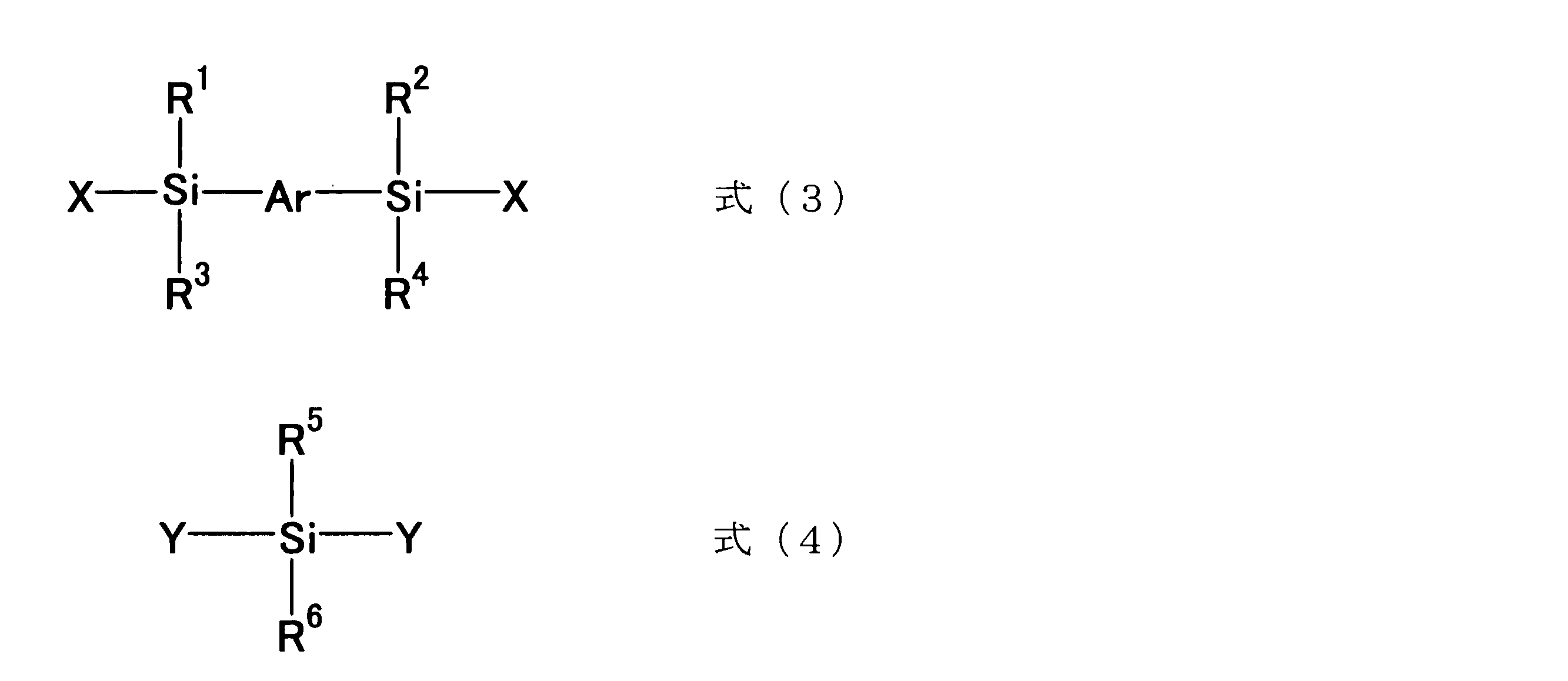
式(3)中、R1~R4およびArは、式(1)中のR1~R4およびArと同義であり、式(4)中、R5およびR6は、式(2)中のR5およびR6と同義であり、式(3)および式(4)中、XおよびYは、それぞれ独立に、水素原子、ヒドロキシ基または加水分解性基を示す。
(viii)上記(i)~(vi)のいずれか一つに記載のオルガノポリシロキサンを架橋させた架橋物である、架橋オルガノポリシロキサン。
(ix)上記架橋が熱架橋である、上記(viii)に記載の架橋オルガノポリシロキサン。
(x)上記(i)~(vi)のいずれか一つに記載のオルガノポリシロキサンと溶剤とを含む、コーティング用組成物。
(ix)上記架橋が熱架橋である、上記(viii)に記載の架橋オルガノポリシロキサン。
(x)上記(i)~(vi)のいずれか一つに記載のオルガノポリシロキサンと溶剤とを含む、コーティング用組成物。
本発明によれば、架橋物としたときに、積層されるガラス基板に対して密着性を有し、かつ、高温処理条件下での分解が抑制されるオルガノポリシロキサンを提供することができる。
[オルガノポリシロキサン]
本発明のオルガノポリシロキサンを説明するにあたって、まず、一般的なオルガノポリシロキサンについて説明する。通常、オルガノポリシロキサンの基本構成単位は、メチル基やフェニル基に代表される1価の有機基がケイ素原子に何個結合しているかで分類され、以下に示すように、D単位と呼ばれる、有機基が2つ結合した2官能性のシロキサン単位、T単位と呼ばれる、有機基が1つ結合した3官能性のシロキサン単位、M単位と呼ばれる、有機基が3つ結合した1官能性のシロキサン単位、および、Q単位と呼ばれる、有機基が1つもない4官能性のシロキサン単位などからなる。なお、Q単位はケイ素原子に結合した有機基(ケイ素原子に結合した炭素原子を有する有機基)を有しない単位であるが、本発明においてはシロキサン単位とみなす。以下の式中、Rはメチル基やフェニル基に代表される1価の有機基を表す。
シロキサン単位において、シロキサン結合は2個のケイ素原子が1個の酸素原子を介して結合した結合であることより、シロキサン結合におけるケイ素原子1個当たりの酸素原子は1/2個とみなし、式中O1/2と表現される。より具体的には、例えば、1つのD単位においては、その1個のケイ素原子は2個の酸素原子と結合し、それぞれの酸素原子は他の単位のケイ素原子と結合していることより、その式は-O1/2-R2Si-O1/2-となる。O1/2が2個存在することより、D単位はR2SiO2/2と表現されるのが通常である。しかし、本発明では、後述のA単位の表現に合わせて、以下のように、個々の酸素原子についてO1/2の表現を用い、M単位、D単位、T単位、Q単位を表現した。
なお、重合体鎖の末端の単位がM単位以外の単位である場合、末端単位のO1/2に結合するケイ素原子以外の原子は1/2個相当の酸素原子であり、合わせて1個の酸素原子となり、水酸基やアルコキシ基などにおける酸素原子を表現する。下記シロキサン単位の表現と同様に表現すれば、例えば末端単位のケイ素原子に結合する水酸基は-O1/2-Hとなる。
本発明のオルガノポリシロキサンを説明するにあたって、まず、一般的なオルガノポリシロキサンについて説明する。通常、オルガノポリシロキサンの基本構成単位は、メチル基やフェニル基に代表される1価の有機基がケイ素原子に何個結合しているかで分類され、以下に示すように、D単位と呼ばれる、有機基が2つ結合した2官能性のシロキサン単位、T単位と呼ばれる、有機基が1つ結合した3官能性のシロキサン単位、M単位と呼ばれる、有機基が3つ結合した1官能性のシロキサン単位、および、Q単位と呼ばれる、有機基が1つもない4官能性のシロキサン単位などからなる。なお、Q単位はケイ素原子に結合した有機基(ケイ素原子に結合した炭素原子を有する有機基)を有しない単位であるが、本発明においてはシロキサン単位とみなす。以下の式中、Rはメチル基やフェニル基に代表される1価の有機基を表す。
シロキサン単位において、シロキサン結合は2個のケイ素原子が1個の酸素原子を介して結合した結合であることより、シロキサン結合におけるケイ素原子1個当たりの酸素原子は1/2個とみなし、式中O1/2と表現される。より具体的には、例えば、1つのD単位においては、その1個のケイ素原子は2個の酸素原子と結合し、それぞれの酸素原子は他の単位のケイ素原子と結合していることより、その式は-O1/2-R2Si-O1/2-となる。O1/2が2個存在することより、D単位はR2SiO2/2と表現されるのが通常である。しかし、本発明では、後述のA単位の表現に合わせて、以下のように、個々の酸素原子についてO1/2の表現を用い、M単位、D単位、T単位、Q単位を表現した。
なお、重合体鎖の末端の単位がM単位以外の単位である場合、末端単位のO1/2に結合するケイ素原子以外の原子は1/2個相当の酸素原子であり、合わせて1個の酸素原子となり、水酸基やアルコキシ基などにおける酸素原子を表現する。下記シロキサン単位の表現と同様に表現すれば、例えば末端単位のケイ素原子に結合する水酸基は-O1/2-Hとなる。

本発明のオルガノポリシロキサンは、概略的には、式(1)で表されるシロキサン単位(A)と式(2)で表されるシロキサン単位(B)とを含むオルガノポリシロキサンである。
シロキサン単位(A)では、2つのケイ素原子のそれぞれが酸素原子と結合し、それぞれの酸素原子は単位外のケイ素原子と結合しているため、式中、O1/2と表現される。シロキサン単位(B)でも同様である。シロキサン単位(A)およびシロキサン単位(B)は2官能性であるから、D単位とみなすことができる。以下、本発明においてシロキサン単位(A)はD単位の1種とみなして、本発明のオルガノポリシロキサンを説明する。
シロキサン単位(A)では、2つのケイ素原子のそれぞれが酸素原子と結合し、それぞれの酸素原子は単位外のケイ素原子と結合しているため、式中、O1/2と表現される。シロキサン単位(B)でも同様である。シロキサン単位(A)およびシロキサン単位(B)は2官能性であるから、D単位とみなすことができる。以下、本発明においてシロキサン単位(A)はD単位の1種とみなして、本発明のオルガノポリシロキサンを説明する。
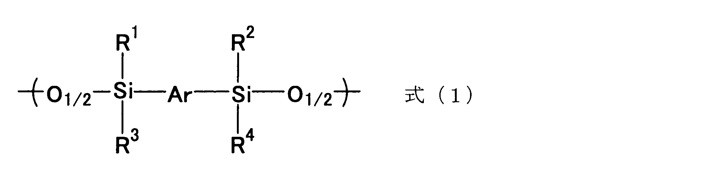
式(1)のR1~R4は、それぞれ独立に、炭素数4以下のアルキル基を表し、Arは、置換基を有していてもよいフェニレン基を表す。なお、Arの2個の結合手は、芳香族環を構成する炭素原子の結合手である。
式(1)のR1~R4が表す炭素数4以下のアルキル基としては、例えば、メチル基、エチル基、n-プロピル基、イソプロピル基、n-ブチル基等が挙げられ、なかでも、高温処理条件下における架橋物の分解がより抑制されるという理由から、メチル基、エチル基が好ましく、メチル基がより好ましく、R1~R4がいずれもメチル基であるのがさらに好ましい。
式(1)中のArが表すフェニレン基が有していてもよい置換基としては、特に限定されず、例えば、ハロゲン原子、脂肪族炭化水素基、芳香族炭化水素基、アルコキシ基、アリールアルキル基、アリールオキシ基、複素環基、アミノ基、ニトロ基、シアノ基等が挙げられるが、Arが表すフェニレン基としては、無置換のフェニレン基であるのが好ましい。
式(1)のR1~R4が表す炭素数4以下のアルキル基としては、例えば、メチル基、エチル基、n-プロピル基、イソプロピル基、n-ブチル基等が挙げられ、なかでも、高温処理条件下における架橋物の分解がより抑制されるという理由から、メチル基、エチル基が好ましく、メチル基がより好ましく、R1~R4がいずれもメチル基であるのがさらに好ましい。
式(1)中のArが表すフェニレン基が有していてもよい置換基としては、特に限定されず、例えば、ハロゲン原子、脂肪族炭化水素基、芳香族炭化水素基、アルコキシ基、アリールアルキル基、アリールオキシ基、複素環基、アミノ基、ニトロ基、シアノ基等が挙げられるが、Arが表すフェニレン基としては、無置換のフェニレン基であるのが好ましい。
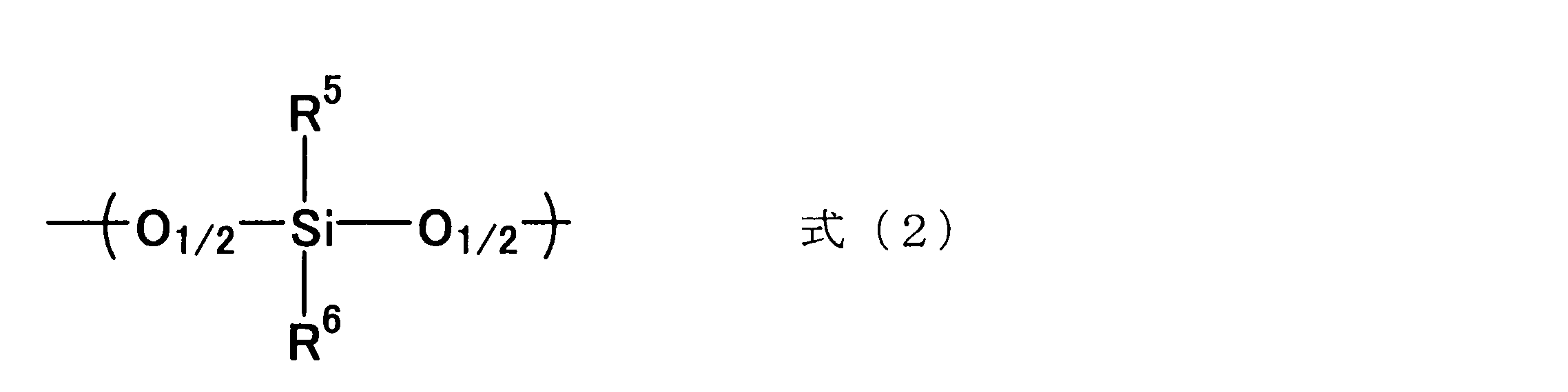
式(2)中、R5およびR6は、それぞれ独立に、炭素数4以下のアルキル基または炭素数3以下のアルケニル基を表す。
式(2)中、R5およびR6が表す炭素数4以下のアルキル基としては、例えば、メチル基、エチル基、n-プロピル基、イソプロピル基、n-ブチル基等が挙げられ、なかでも、高温処理条件下における架橋物の分解がより抑制されるという理由から、メチル基、エチル基が好ましく、メチル基がより好ましい。
式(2)中、R5およびR6が表す炭素数3以下のアルケニル基としては、ビニル基、アリル基が挙げられ、なかでも、高温処理条件下における架橋物の分解がより抑制されるという理由から、ビニル基が好ましい。
なお、式(2)で表わされるシラン化合物は、R5およびR6の一方が炭素数3以下のアルケニル基であり他方が炭素数4以下のアルキル基であるシラン化合物、R5およびR6の両方がそれぞれ炭素数3以下のアルケニル基であるシラン化合物、ならびに、R5およびR6のいずれもがそれぞれ炭素数4以下のアルキル基であるシラン化合物からなる。
式(2)中、R5およびR6が表す炭素数4以下のアルキル基としては、例えば、メチル基、エチル基、n-プロピル基、イソプロピル基、n-ブチル基等が挙げられ、なかでも、高温処理条件下における架橋物の分解がより抑制されるという理由から、メチル基、エチル基が好ましく、メチル基がより好ましい。
式(2)中、R5およびR6が表す炭素数3以下のアルケニル基としては、ビニル基、アリル基が挙げられ、なかでも、高温処理条件下における架橋物の分解がより抑制されるという理由から、ビニル基が好ましい。
なお、式(2)で表わされるシラン化合物は、R5およびR6の一方が炭素数3以下のアルケニル基であり他方が炭素数4以下のアルキル基であるシラン化合物、R5およびR6の両方がそれぞれ炭素数3以下のアルケニル基であるシラン化合物、ならびに、R5およびR6のいずれもがそれぞれ炭素数4以下のアルキル基であるシラン化合物からなる。
本発明のオルガノポリシロキサンにおいては、シロキサン単位(A)とシロキサン単位(B)との合計に対するシロキサン単位(A)の割合は、高温処理条件下における架橋物の分解が抑制されるとともに、架橋物のガラス基板に対する密着性および剥離性も良好になるという理由から、30~60モル%であり、35~55モル%であるのが好ましく、45~55モル%であるのがより好ましい。
また、本発明のオルガノポリシロキサンは、例えば、M単位、T単位、Q単位などの他のシロキサン単位を含んでいてもよいが、全シロキサン単位に対するシロキサン単位(A)とシロキサン単位(B)との合計の割合は、90~100モル%であり、架橋物のガラス基板に対する密着性および剥離性がより良好になるという理由から、95~100モル%が好ましく、97~100モル%がより好ましい。
本発明のオルガノポリシロキサンが他のシロキサン単位を含む場合、その単位はM単位であることが好ましい。M単位としては、ケイ素原子に結合する3個の有機基がすべて炭素数4以下のアルキル基である単位、または、ケイ素原子に結合する1個の有機基が炭素数3以下のアルケニル基であり2個の有機基が炭素数4以下のアルキル基である単位が好ましい。ここで、炭素数4以下のアルキル基としてはメチル基およびエチル基が好ましく、炭素数3以下のアルケニル基としてはビニル基が好ましい。M単位を含む場合、全シロキサン単位に対するM単位の割合は、1~10モル%が好ましく、2~7モル%がより好ましい。この範囲でM単位を有すると分子量の調節が容易となる。また、M単位を含むとオルガノポリシロキサンの末端からの開裂が抑制されるので、耐熱性が向上する。
本発明のオルガノポリシロキサンがT単位(その有機基としては炭素数4以下のアルキル基が好ましい)やQ単位を含む場合、全シロキサン単位に対するそれらの単位の合計の割合は、5モル%以下が好ましく、3モル%以下がより好ましい。T単位やQ単位が存在すると架橋オルガノポリシロキサンの柔軟性が低下するおそれがあることから、本発明のオルガノポリシロキサンはT単位やQ単位を含まないことが特に好ましい。
本発明のオルガノポリシロキサンがT単位(その有機基としては炭素数4以下のアルキル基が好ましい)やQ単位を含む場合、全シロキサン単位に対するそれらの単位の合計の割合は、5モル%以下が好ましく、3モル%以下がより好ましい。T単位やQ単位が存在すると架橋オルガノポリシロキサンの柔軟性が低下するおそれがあることから、本発明のオルガノポリシロキサンはT単位やQ単位を含まないことが特に好ましい。
なお、本発明のオルガノポリシロキサンは、T単位および/またはQ単位を含むと、硬化物の耐熱性は向上するが、柔軟性が低下して密着性が劣ったり、また、剥離性も低下する場合があるため、密着性および剥離性の観点からは、T単位およびQ単位を含まないのが好ましい。
本発明のオルガノポリシロキサンが含むM単位としては、特に限定されないが、例えば、下記式(S)で表されるシロキサン単位が挙げられる。
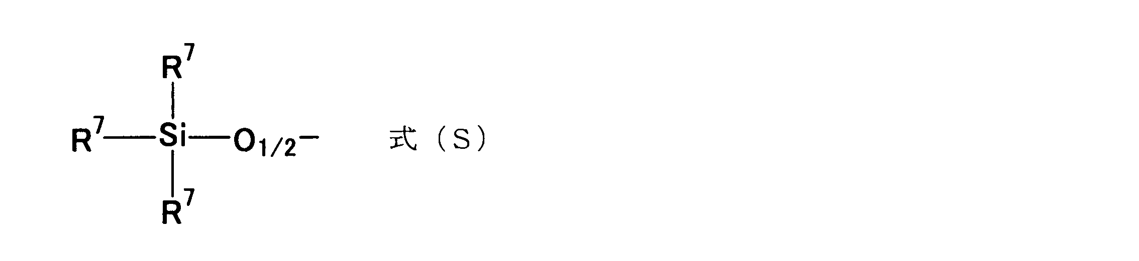
式(S)中、R7は、それぞれ独立に、炭素数6以下の炭化水素基を表す。R7が示す炭化水素基としては、例えば、アルキル基、アリール基、アルケニル基等が挙げられる。ここで、アルキル基の具体例としては、メチル基、エチル基、n-プロピル基、イソプロピル基、n-ブチル基等が挙げられ、なかでも、メチル基、エチル基が好ましく、メチル基がより好ましい。また、アリール基の具体例としては、フェニル基が挙げられ、アルケニル基の具体例としては、ビニル基が挙げられる。
そして、本発明のオルガノポリシロキサンにおいて、シロキサン単位(B)は、R5およびR6の少なくとも一方が炭素数3以下のアルケニル基であり該アルケニル基以外の場合のR5およびR6が炭素数4以下のアルキル基であるシロキサン単位(B-1)、ならびに、R5およびR6のいずれもがそれぞれ炭素数4以下のアルキル基であるシロキサン単位(B-2)からなる。
シロキサン単位(B-1)の好適態様としては、高温処理条件下における架橋物の分解がより抑制されるという理由から、R5またはR6の一方がメチル基で、他方がビニル基である態様が挙げられる。
シロキサン単位(B-2)の好適態様としては、R5およびR6のいずれもがメチル基である態様が挙げられる。
シロキサン単位(B-2)の好適態様としては、R5およびR6のいずれもがメチル基である態様が挙げられる。
さらに、本発明においては、全シロキサン単位(B)に対するシロキサン単位(B-1)の割合である[シロキサン単位(B-1)]×100/[シロキサン単位(B-1)+シロキサン単位(B-2)]が、25~90モル%である。高温処理条件下における架橋物の分解がより抑制されるとともに、架橋物のガラス基板に対する密着性および剥離性もより良好になるというという理由から、上記割合は25~75モル%であるのが好ましく、45~55モル%であるのがより好ましい。
本発明のオルガノポリシロキサン中におけるシロキサン単位(A)およびシロキサン単位(B)の結合形式は、特に限定されず、例えば、ランダム共重合体、ブロック共重合体、交互共重合体等が挙げられ、なかでも、高温処理条件下における架橋物の分解がより抑制されるという理由から、交互共重合体であることが好ましい。
本発明において、シロキサン単位(A)とシロキサン単位(B)との交互共重合体とは、シロキサン単位(A)とシロキサン単位(B)との結合が、シロキサン単位(A)とシロキサン単位(A)との結合およびシロキサン単位(B)とシロキサン単位(B)との結合の合計よりもはるかに多い共重合体を意味する。
これら3種の結合は、例えば1H NMR測定および29Si NMR測定により区別することができ、その測定によりそれら結合の相対的な数の割合を計算できる。
本発明におけるシロキサン単位(A)とシロキサン単位(B)との交互共重合体は、少数のランダム結合部分やブロック結合部分を含んでいてもよい。
交互共重合体におけるシロキサン単位(A)とシロキサン単位(B)との結合の割合は、上記3種の結合の合計に対して、90~100モル%が好ましく、95~100モル%がより好ましい。
なお、交互共重合体であるか否かを区別するものではないが、本発明のポリシロキサンが交互共重合体である場合、その交互共重合体におけるシロキサン単位(A)およびシロキサン単位(B)の合計に対するシロキサン単位(A)の割合は50±5モル%が好ましい。
交互共重合性の分析方法については、例えば、Journal of Applied Polymer Science, Vol. 106, 1007-1013 (2007)を参考できる。
これら3種の結合は、例えば1H NMR測定および29Si NMR測定により区別することができ、その測定によりそれら結合の相対的な数の割合を計算できる。
本発明におけるシロキサン単位(A)とシロキサン単位(B)との交互共重合体は、少数のランダム結合部分やブロック結合部分を含んでいてもよい。
交互共重合体におけるシロキサン単位(A)とシロキサン単位(B)との結合の割合は、上記3種の結合の合計に対して、90~100モル%が好ましく、95~100モル%がより好ましい。
なお、交互共重合体であるか否かを区別するものではないが、本発明のポリシロキサンが交互共重合体である場合、その交互共重合体におけるシロキサン単位(A)およびシロキサン単位(B)の合計に対するシロキサン単位(A)の割合は50±5モル%が好ましい。
交互共重合性の分析方法については、例えば、Journal of Applied Polymer Science, Vol. 106, 1007-1013 (2007)を参考できる。
本発明のオルガノポリシロキサンの数平均分子量は特に限定されないが、取扱い性に優れると共に、成膜性にも優れ、高温処理条件下における架橋物の分解がより抑制されるという理由から、GPC(ゲルパーミエーションクロマトグラフィー)測定によるポリスチレン換算の数平均分子量が、5,000~30,000であるのが好ましく、10,000~18,000であるのがより好ましい。
本発明のオルガノポリシロキサンの数平均分子量の調整は、反応条件を制御することにより行うことができる。例えば、本発明のオルガノポリシロキサンを製造する際の溶媒量を調整し、モノマーの濃度を高くすると高分子量物が得られ、濃度を低くすると低分子量物が得られる。
本発明のオルガノポリシロキサンの数平均分子量の調整は、反応条件を制御することにより行うことができる。例えば、本発明のオルガノポリシロキサンを製造する際の溶媒量を調整し、モノマーの濃度を高くすると高分子量物が得られ、濃度を低くすると低分子量物が得られる。
〔オルガノポリシロキサンの製造方法〕
本発明のオルガノポリシロキサンの製造方法としては、特に限定されず、例えば、Macromolecules 1998, 31, 850-856、Journal of Applied Polymer Science, Vol.106, 1007, 2007等の公知文献に記載された方法を採用できる。
本発明のオルガノポリシロキサンの製造方法としては、特に限定されず、例えば、Macromolecules 1998, 31, 850-856、Journal of Applied Polymer Science, Vol.106, 1007, 2007等の公知文献に記載された方法を採用できる。
本発明のオルガノポリシロキサンが、シロキサン単位(A)とシロキサン単位(B)との交互共重合体(以下、単に「交互共重合体」ともいう)である場合、交互共重合体は、反応性が異なる2種の単量体を重合させることにより得ることができる。
例えば、シロキサン単位(A)となる下記式(3)で表されるシラン化合物が有する重合反応性基であるXと、シロキサン単位(B)となる下記式(4)で表されるシラン化合物が有する重合反応性基であるYとの相互の反応性が、Xどうしの反応性およびYどうしの反応性のいずれよりも高くなるものを選択して、上記2種のシラン化合物の実質的に等モル量を反応させることにより、交互共重合体を製造することができる。XとYとの反応性が、Xどうしの反応性およびYどうしの反応性のいずれよりもより高いものとすることにより、ランダム結合部分やブロック結合部分のより少ない交互共重合体が得られる。
交互共重合体を製造する場合、XおよびYの一方がヒドロキシ基であり、他方がアミノ基、モノアルキルアミノ基、ジアルキルアミノ基などの1~3級のアミノ基であることが好ましい。特に、一方がヒドロキシ基で他方がジアルキルアミノ基であることが好ましく、Xがヒドロキシ基でYがジアルキルアミノ基であることがより好ましい。なお、モノアルキルアミノ基やジアルキルアミノ基におけるアルキル基としては、炭素数4以下のアルキル基が好ましく、メチル基が特に好ましい。
本発明における交互共重合体の製造方法としては、例えば、例えば、Macromolecules 1998, 31, 850-856、Journal of Applied Polymer Science, Vol.106, 1007, 2007等の公知文献に記載された方法を採用できる。
例えば、シロキサン単位(A)となる下記式(3)で表されるシラン化合物が有する重合反応性基であるXと、シロキサン単位(B)となる下記式(4)で表されるシラン化合物が有する重合反応性基であるYとの相互の反応性が、Xどうしの反応性およびYどうしの反応性のいずれよりも高くなるものを選択して、上記2種のシラン化合物の実質的に等モル量を反応させることにより、交互共重合体を製造することができる。XとYとの反応性が、Xどうしの反応性およびYどうしの反応性のいずれよりもより高いものとすることにより、ランダム結合部分やブロック結合部分のより少ない交互共重合体が得られる。
交互共重合体を製造する場合、XおよびYの一方がヒドロキシ基であり、他方がアミノ基、モノアルキルアミノ基、ジアルキルアミノ基などの1~3級のアミノ基であることが好ましい。特に、一方がヒドロキシ基で他方がジアルキルアミノ基であることが好ましく、Xがヒドロキシ基でYがジアルキルアミノ基であることがより好ましい。なお、モノアルキルアミノ基やジアルキルアミノ基におけるアルキル基としては、炭素数4以下のアルキル基が好ましく、メチル基が特に好ましい。
本発明における交互共重合体の製造方法としては、例えば、例えば、Macromolecules 1998, 31, 850-856、Journal of Applied Polymer Science, Vol.106, 1007, 2007等の公知文献に記載された方法を採用できる。
より詳細には、例えば、下記式(3)で表されるシラン化合物と、下記式(4)で表されるシラン化合物とを、トルエン等の溶媒中で撹拌等しながら加熱する方法が挙げられ、具体的には、例えば、下記式(3)で表されるシラン化合物を溶媒に添加したものと、下記式(4)で表されるシラン化合物を溶媒に添加したものとを別々に準備し、一方を他方に、5~10分かけて滴下して、その後、1~1.5時間反応させる方法;下記式(3)で表されるシラン化合物と、下記式(4)で表されるシラン化合物とを、溶媒中に同時に添加し、1~2時間反応させる方法;等が挙げられる。
ここで、反応させる各シラン化合物の割合は、下記式(3)で表されるシラン化合物が30~60モル%であるのが好ましく、下記式(4)で表されるシラン化合物が70~40モル%であるのが好ましい。
また、このとき、80~110℃の温度範囲で加熱するのが好ましく、90~110℃の温度範囲で加熱するのがより好ましい。必要により反応触媒を使用することもできる。
ここで、反応させる各シラン化合物の割合は、下記式(3)で表されるシラン化合物が30~60モル%であるのが好ましく、下記式(4)で表されるシラン化合物が70~40モル%であるのが好ましい。
また、このとき、80~110℃の温度範囲で加熱するのが好ましく、90~110℃の温度範囲で加熱するのがより好ましい。必要により反応触媒を使用することもできる。

式(3)中、R1~R4およびArは、式(1)中のR1~R4およびArと同義であり、式(4)中、R5およびR6は、式(2)中のR5およびR6と同義である。また、式(3)および式(4)中、XおよびYは、それぞれ独立に、水素原子、ヒドロキシ基または加水分解性基を示す。ここで、加水分解性基としては、例えば、塩素原子、アルコキシ基、アシル基、アミノ基、2級アミノ基、3級アミノ基、イソシアネート基等が挙げられる。
上記加水分解性基であるアルコキシ基としては、炭素数4以下のアルコキシ基が好ましく、メトキシ基、エトキシ基がより好ましい。また、アシル基としては、炭素数5以下のアシル基が好ましい。2級アミノ基としてはモノアルキルアミノ基が好ましく、3級アミノ基としてはジアルキルアミノ基が好ましく、それぞれにおけるアルキル基としてはいずれも炭素数4以下のアルキル基が好ましい。
なお、式(4)で表わされるシラン化合物は、R5およびR6の一方が炭素数3以下のアルケニル基であり他方が炭素数4以下のアルキル基であるシラン化合物、R5およびR6の両方がそれぞれ炭素数3以下のアルケニル基であるシラン化合物、ならびに、R5およびR6のいずれもがそれぞれ炭素数4以下のアルキル基であるシラン化合物からなる。
上記加水分解性基であるアルコキシ基としては、炭素数4以下のアルコキシ基が好ましく、メトキシ基、エトキシ基がより好ましい。また、アシル基としては、炭素数5以下のアシル基が好ましい。2級アミノ基としてはモノアルキルアミノ基が好ましく、3級アミノ基としてはジアルキルアミノ基が好ましく、それぞれにおけるアルキル基としてはいずれも炭素数4以下のアルキル基が好ましい。
なお、式(4)で表わされるシラン化合物は、R5およびR6の一方が炭素数3以下のアルケニル基であり他方が炭素数4以下のアルキル基であるシラン化合物、R5およびR6の両方がそれぞれ炭素数3以下のアルケニル基であるシラン化合物、ならびに、R5およびR6のいずれもがそれぞれ炭素数4以下のアルキル基であるシラン化合物からなる。
なお、式(3)で表されるシラン化合物と、式(4)で表されるシラン化合物とを反応させるに際しては、分子量制御等の観点から、さらに下記式(S′)で表されるシラン化合物を配合してもよい。

式(S′)中、R7は、式(S)中のR7と同義であり、Zは重合性反応基を示す。Zが示す重合性反応基としては、例えば、ヒドロキシ基;アミノ基、モノアルキルアミノ基、ジアルキルアミノ基などの1~3級のアミノ基;等が挙げられる。
上記のような本発明のオルガノポリシロキサンの製造方法の一態様を説明すると、例えば、式(5)で表されるジシラノール化合物と、式(6)で表されるジアミノシラン化合物とを重縮合反応させて、本発明のオルガノポリシロキサンを得る方法が挙げられる。
この重縮合反応では、具体的には、式(5)中の「-OH」と式(6)中の「-N(CH3)2」とが反応し、副生成物のアミンとして「(CH3)2NH」を与えて、主生成物として本発明の交互共重合体を生成する。
この重縮合反応では、具体的には、式(5)中の「-OH」と式(6)中の「-N(CH3)2」とが反応し、副生成物のアミンとして「(CH3)2NH」を与えて、主生成物として本発明の交互共重合体を生成する。
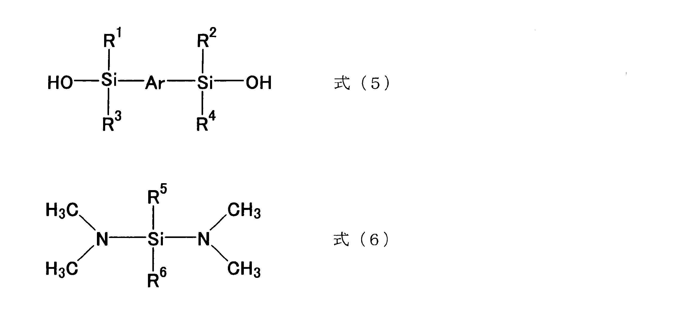
式(5)中、R1~R4およびArは、式(1)中のR1~R4およびArと同義であり、式(6)中のR5およびR6は、式(2)中のR5およびR6と同義である。なお、式(5)中の「-OH」は、例えば、ハロゲン基、アルコキシ基などの加水分解性基の加水分解により供されるものであってもよい。
また、交互共重合体である本発明のオルガノポリシロキサンは、式(3)中のXが水素原子である式(7)で表されるジヒドロシラン化合物と、式(4)中のYがアルコキシ基である式(8)で表されるジアルコキシシラン化合物とから製造することもできる。具体的には、例えば、式(7)で表されるジヒドロシラン化合物と、式(8)で表されるジアルコキシシラン化合物とを、トリス(ペンタフルオロフェニル)ボラン(B(C6F5)3)等の有機ボランの存在下で反応させて、交互共重合体である本発明のオルガノポリシロキサンを得る方法が挙げられる。
この反応では、具体的には、式(7)中の「-H」と式(8)中の「-OR」とが反応し、副生成物として「RH(例えば、CH4)」を与えて、主生成物として本発明のオルガノポリシロキサンを生成する。
この反応では、具体的には、式(7)中の「-H」と式(8)中の「-OR」とが反応し、副生成物として「RH(例えば、CH4)」を与えて、主生成物として本発明のオルガノポリシロキサンを生成する。

式(7)中、R1~R4およびArは、式(1)中のR1~R4およびArと同義であり、式(8)中のR5およびR6は、式(2)中のR5およびR6と同義である。なお、式(8)中のRは、メチル基(-CH3)、エチル基(-C2H5)などの炭素数1~5のアルキル基を示す。
この反応の条件等は特に限定されず、例えば、25~40℃の温度範囲で、3~5時間反応させるのが好ましい。
[架橋オルガノポリシロキサン(オルガノポリシロキサンの架橋物)]
本発明の架橋オルガノポリシロキサンは、上述した本発明のオルガノポリシロキサンを架橋させた架橋物である。すなわち、本発明のオルガノポリシロキサンは、所定の架橋反応を介して、架橋硬化し、架橋物(硬化物)となる。
なお、以下、本発明のオルガノポリシロキサンを架橋硬化させて架橋物を形成することを、単に、本発明のオルガノポリシロキサンの硬化ともいう。
本発明の架橋オルガノポリシロキサンは、上述した本発明のオルガノポリシロキサンを架橋させた架橋物である。すなわち、本発明のオルガノポリシロキサンは、所定の架橋反応を介して、架橋硬化し、架橋物(硬化物)となる。
なお、以下、本発明のオルガノポリシロキサンを架橋硬化させて架橋物を形成することを、単に、本発明のオルガノポリシロキサンの硬化ともいう。
架橋の形式は特に限定されず、本発明のオルガノポリシロキサン中に含まれる架橋性基の種類に応じて適宜公知の形式を採用でき、例えば、ヒドロシリル化反応、縮合反応、ラジカル反応などが挙げられる。
もっとも、式(2)で表されるシロキサン単位(B)を含む本発明のオルガノポリシロキサンは、ラジカル反応性基であるアルケニル基を有するため、原則的に、ラジカル反応を介した形式が採用される。
また、ここで採用されるラジカル反応としては、例えば、加熱処理による反応、高エネルギー線処理による反応、ラジカル重合開始剤による反応などが挙げられるが、扱いやすさの観点から、加熱処理による反応であるのが好ましい。
以下、加熱処理によるラジカル反応を介した架橋を「熱架橋」ともいう。本発明の架橋オルガノポリシロキサンは、上述した本発明のオルガノポリシロキサンを熱架橋させて得られる架橋物であるのが好ましい。
なお、熱架橋の好適条件等については、後述する「樹脂層形成工程」にて説明する。
もっとも、式(2)で表されるシロキサン単位(B)を含む本発明のオルガノポリシロキサンは、ラジカル反応性基であるアルケニル基を有するため、原則的に、ラジカル反応を介した形式が採用される。
また、ここで採用されるラジカル反応としては、例えば、加熱処理による反応、高エネルギー線処理による反応、ラジカル重合開始剤による反応などが挙げられるが、扱いやすさの観点から、加熱処理による反応であるのが好ましい。
以下、加熱処理によるラジカル反応を介した架橋を「熱架橋」ともいう。本発明の架橋オルガノポリシロキサンは、上述した本発明のオルガノポリシロキサンを熱架橋させて得られる架橋物であるのが好ましい。
なお、熱架橋の好適条件等については、後述する「樹脂層形成工程」にて説明する。
このような本発明の架橋オルガノポリシロキサンは、高温処理条件下における分解が抑制される。その理由としては、本発明のオルガノポリシロキサン中にフェニレン基が含まれている点が挙げられる。このフェニレン基が含まれることにより、本発明のオルガノポリシロキサン(本発明の架橋オルガノポリシロキサン)の結合エネルギーが向上すると共に、運動性が低下し、シロキサン結合の開裂が進行しにくくなる。結果として、開裂に伴い生成するシロキサンの環状化合物の発生が抑制され、アウトガスの発生や、ガラス基板の位置ずれなどがより抑制される。
本発明の架橋オルガノポリシロキサンは、優れた耐熱性を有する。具体的には、本発明の架橋オルガノポリシロキサンの5%重量減少温度は、450℃以上が好ましく、500℃以上がより好ましい。上限は特に制限されないが、通常、600℃以下の場合が多い。上記範囲内であれば、例えば本発明の架橋オルガノポリシロキサンを樹脂層とする上述したガラス積層体において、TFTアレイの製造プロセスなど高温条件(約400℃以上)下においても、架橋オルガノポリシロキサンの分解が抑制され、発泡の発生などがより抑制される。
なお、上記5%重量減少温度は、熱重量分析装置を用いて、昇温速度15℃/分、窒素雰囲気下(100mL/分)で試料を室温~700℃まで昇温した際に、試料の重量が5%減少する温度をいう。
なお、上記5%重量減少温度は、熱重量分析装置を用いて、昇温速度15℃/分、窒素雰囲気下(100mL/分)で試料を室温~700℃まで昇温した際に、試料の重量が5%減少する温度をいう。
また、本発明の架橋オルガノポリシロキサンは、ガラス基板に対する密着性にも優れる。これは、架橋に寄与するアルケニル基を有するシロキサン単位(B-1)の割合が上述した本発明の範囲の上限値以下であることにより、本発明の架橋オルガノポリシロキサンは硬くなりすぎず柔軟性を有し密着性を発揮するためと考えられる。
また、本発明の架橋オルガノポリシロキサンは、シロキサン単位(B-1)の割合が上述した本発明の範囲の下限値以上であることにより、粘性液体状のままで固まらずガラス基板から容易に剥離できないといった事態が回避され、剥離性にも優れる。
また、本発明の架橋オルガノポリシロキサンは、シロキサン単位(B-1)の割合が上述した本発明の範囲の下限値以上であることにより、粘性液体状のままで固まらずガラス基板から容易に剥離できないといった事態が回避され、剥離性にも優れる。
[コーティング用組成物]
本発明のコーティング用組成物は、上述した本発明のオルガノポリシロキサンと溶剤とを含む組成物である。
後述するように、本発明のオルガノポリシロキサンの層を、所定の基材表面に形成し、この表面上で本発明のオルガノポリシロキサンを架橋させて、本発明の架橋オルガノポリシロキサンの層を形成することができるが、このとき、本発明のコーティング用組成物を用いるのが好ましい。
具体的には、本発明のコーティング用組成物を使用し、この組成物を支持基材上に塗布して溶液の層を形成し、次いで溶剤を除去して本発明のオルガノポリシロキサンの層とすることが好ましい。組成物中における本発明のオルガノポリシロキサンの濃度の調整などにより、層の厚さを制御することができる。
溶剤としては、作業環境下で本発明のオルガノポリシロキサンを容易に溶解でき、かつ、容易に揮発除去させることのできるものであれば、特に限定されず、例えば、トルエン、キシレン、テトラヒドロフラン(THF)、クロロホルム等が挙げられる。
本発明のコーティング用組成物は、上述した本発明のオルガノポリシロキサンと溶剤とを含む組成物である。
後述するように、本発明のオルガノポリシロキサンの層を、所定の基材表面に形成し、この表面上で本発明のオルガノポリシロキサンを架橋させて、本発明の架橋オルガノポリシロキサンの層を形成することができるが、このとき、本発明のコーティング用組成物を用いるのが好ましい。
具体的には、本発明のコーティング用組成物を使用し、この組成物を支持基材上に塗布して溶液の層を形成し、次いで溶剤を除去して本発明のオルガノポリシロキサンの層とすることが好ましい。組成物中における本発明のオルガノポリシロキサンの濃度の調整などにより、層の厚さを制御することができる。
溶剤としては、作業環境下で本発明のオルガノポリシロキサンを容易に溶解でき、かつ、容易に揮発除去させることのできるものであれば、特に限定されず、例えば、トルエン、キシレン、テトラヒドロフラン(THF)、クロロホルム等が挙げられる。
[架橋オルガノポリシロキサンの層を有する基材の製造方法]
ここで、上述した本発明の架橋オルガノポリシロキサンの層を有する基材を製造する方法について記載する。なお、以下では、便宜的に、本発明の架橋オルガノポリシロキサンの層を「シリコーン樹脂層」ともいい、シリコーン樹脂層を有する基材を「シリコーン樹脂層付き基材」ともいい、シリコーン樹脂層付き基材を製造する方法を「本発明の樹脂層付き基材の製造方法」ともいう。
本発明の樹脂層付き基材の製造方法は、概略的には、上述した本発明のコーティング用組成物を基材に塗布し、溶剤を除去して基材上に本発明のオルガノポリシロキサンの層を形成し、次いで、本発明のオルガノポリシロキサンを架橋させることにより、架橋オルガノポリシロキサンの層(シリコーン樹脂層)とし、シリコーン樹脂層付き基材を得る方法であり、ガラス積層体の製造方法が有する樹脂層形成工程(後述)を構成する。したがって、本発明の樹脂層付き基材の製造方法の説明としては、樹脂層形成工程についての記載も参照されたい。
ここで、上述した本発明の架橋オルガノポリシロキサンの層を有する基材を製造する方法について記載する。なお、以下では、便宜的に、本発明の架橋オルガノポリシロキサンの層を「シリコーン樹脂層」ともいい、シリコーン樹脂層を有する基材を「シリコーン樹脂層付き基材」ともいい、シリコーン樹脂層付き基材を製造する方法を「本発明の樹脂層付き基材の製造方法」ともいう。
本発明の樹脂層付き基材の製造方法は、概略的には、上述した本発明のコーティング用組成物を基材に塗布し、溶剤を除去して基材上に本発明のオルガノポリシロキサンの層を形成し、次いで、本発明のオルガノポリシロキサンを架橋させることにより、架橋オルガノポリシロキサンの層(シリコーン樹脂層)とし、シリコーン樹脂層付き基材を得る方法であり、ガラス積層体の製造方法が有する樹脂層形成工程(後述)を構成する。したがって、本発明の樹脂層付き基材の製造方法の説明としては、樹脂層形成工程についての記載も参照されたい。
[ガラス積層体]
次に、本発明の樹脂層付き基材の製造方法およびシリコーン樹脂層付き基材の説明を兼ねて、ガラス積層体について説明する。ガラス積層体は、基材(以下、「支持基材」ともいう。)の層とガラス基板の層との間にシリコーン樹脂層を有する。
ガラス積層体においては、シリコーン樹脂層が、上述した本発明の架橋オルガノポリシロキサンの層であることにより、ガラス基板に対して優れた密着性を示すと共に、高温処理条件下においてシリコーン樹脂層の分解が抑制される。結果として、アウトガスの発生や、ガラス基板の位置ずれなどがより抑制される。
次に、本発明の樹脂層付き基材の製造方法およびシリコーン樹脂層付き基材の説明を兼ねて、ガラス積層体について説明する。ガラス積層体は、基材(以下、「支持基材」ともいう。)の層とガラス基板の層との間にシリコーン樹脂層を有する。
ガラス積層体においては、シリコーン樹脂層が、上述した本発明の架橋オルガノポリシロキサンの層であることにより、ガラス基板に対して優れた密着性を示すと共に、高温処理条件下においてシリコーン樹脂層の分解が抑制される。結果として、アウトガスの発生や、ガラス基板の位置ずれなどがより抑制される。
図1は、ガラス積層体の一例を模式的に示す断面図である。
図1に示すように、ガラス積層体10においては、支持基材12の層とガラス基板16の層とそれらの間にシリコーン樹脂層14が存在する。シリコーン樹脂層14は、その一方の面が支持基材12の層に接すると共に、その他方の面がガラス基板16の第1主面16aに接している。言い換えると、シリコーン樹脂層14はガラス基板16の第1主面16aに接している。
支持基材12の層およびシリコーン樹脂層14からなる2層部分は、液晶パネルなどの電子デバイス用部材を製造する部材形成工程において、ガラス基板16を補強する。そして、ガラス積層体10の製造のためにあらかじめ製造される支持基材12の層およびシリコーン樹脂層14からなる2層部分が、「シリコーン樹脂層付き基材18」である。
図1に示すように、ガラス積層体10においては、支持基材12の層とガラス基板16の層とそれらの間にシリコーン樹脂層14が存在する。シリコーン樹脂層14は、その一方の面が支持基材12の層に接すると共に、その他方の面がガラス基板16の第1主面16aに接している。言い換えると、シリコーン樹脂層14はガラス基板16の第1主面16aに接している。
支持基材12の層およびシリコーン樹脂層14からなる2層部分は、液晶パネルなどの電子デバイス用部材を製造する部材形成工程において、ガラス基板16を補強する。そして、ガラス積層体10の製造のためにあらかじめ製造される支持基材12の層およびシリコーン樹脂層14からなる2層部分が、「シリコーン樹脂層付き基材18」である。
ガラス積層体10は、後述する部材形成工程まで使用される。すなわち、ガラス積層体10は、そのガラス基板16の第2主面16b表面上に液晶表示装置などの電子デバイス用部材が形成されるまで使用される。その後、電子デバイス用部材が形成された積層体は、シリコーン樹脂層付き基材18と部材付きガラス基板とに分離され、シリコーン樹脂層付き基材18は電子デバイスを構成する部分とはならない。シリコーン樹脂層付き基材18は、新たなガラス基板16と積層され、新たなガラス積層体10として再利用することができる。
支持基材12とシリコーン樹脂層14との界面は剥離強度(x)を有し、支持基材12とシリコーン樹脂層14との界面に剥離強度(x)を越える引き剥がし方向の応力が加えられると、支持基材12とシリコーン樹脂層14との界面が剥離する。シリコーン樹脂層14とガラス基板16との界面は剥離強度(y)を有し、シリコーン樹脂層14とガラス基板16との界面に剥離強度(y)を越える引き剥がし方向の応力が加えられると、シリコーン樹脂14層とガラス基板16との界面が剥離する。
ガラス積層体10(後述の電子デバイス用部材付き積層体も意味する)においては、上記剥離強度(x)は上記剥離強度(y)よりも高い。したがって、ガラス積層体10に支持基材12とガラス基板16とを引き剥がす方向の応力が加えられると、シリコーン樹脂層14とガラス基板16との界面で剥離して、ガラス基板16とシリコーン樹脂層付き基材18とに分離する。
ガラス積層体10(後述の電子デバイス用部材付き積層体も意味する)においては、上記剥離強度(x)は上記剥離強度(y)よりも高い。したがって、ガラス積層体10に支持基材12とガラス基板16とを引き剥がす方向の応力が加えられると、シリコーン樹脂層14とガラス基板16との界面で剥離して、ガラス基板16とシリコーン樹脂層付き基材18とに分離する。
剥離強度(x)は、剥離強度(y)と比較して、充分高いことが好ましい。剥離強度(x)を高めることは、支持基材12に対するシリコーン樹脂層14の付着力を高め、かつ加熱処理後においてガラス基板16に対してよりも相対的に高い付着力を維持できることを意味する。
支持基材12に対するシリコーン樹脂層14の付着力を高めるためには、本発明のオルガノポリシロキサンを支持基材12上で硬化させてシリコーン樹脂層14を形成することが好ましい。硬化の際の接着力で、支持基材12に対して高い結合力で結合したシリコーン樹脂層14を形成することができる。
一方、硬化後の本発明のオルガノポリシロキサンの架橋物(本発明の架橋オルガノポリシロキサン)のガラス基板16に対する結合力は、上記硬化時に生じる結合力よりも低いのが通例である。したがって、支持基材12上で本発明のオルガノポリシロキサンを硬化させてシリコーン樹脂層14を形成し、その後シリコーン樹脂層14の面にガラス基板16を積層して、ガラス積層体10を製造することが好ましい。
支持基材12に対するシリコーン樹脂層14の付着力を高めるためには、本発明のオルガノポリシロキサンを支持基材12上で硬化させてシリコーン樹脂層14を形成することが好ましい。硬化の際の接着力で、支持基材12に対して高い結合力で結合したシリコーン樹脂層14を形成することができる。
一方、硬化後の本発明のオルガノポリシロキサンの架橋物(本発明の架橋オルガノポリシロキサン)のガラス基板16に対する結合力は、上記硬化時に生じる結合力よりも低いのが通例である。したがって、支持基材12上で本発明のオルガノポリシロキサンを硬化させてシリコーン樹脂層14を形成し、その後シリコーン樹脂層14の面にガラス基板16を積層して、ガラス積層体10を製造することが好ましい。
以下では、まず、ガラス積層体10を構成する各層(ガラス基板16、支持基材12、シリコーン樹脂層14)について詳述する。
〔ガラス基板〕
ガラス基板16は、第1主面16aがシリコーン樹脂層14と接し、シリコーン樹脂層14側とは反対側の第2主面16bに電子デバイス用部材が設けられる。
ガラス基板16の種類は、一般的なものであってよく、例えば、LCD、OLEDといった表示装置用のガラス基板などが挙げられる。ガラス基板16は耐薬品性、耐透湿性に優れ、かつ、熱収縮率が低いことが好ましい。熱収縮率の指標としては、JIS R 3102(1995年改正)に規定されている線膨張係数が用いられる。
ガラス基板16は、第1主面16aがシリコーン樹脂層14と接し、シリコーン樹脂層14側とは反対側の第2主面16bに電子デバイス用部材が設けられる。
ガラス基板16の種類は、一般的なものであってよく、例えば、LCD、OLEDといった表示装置用のガラス基板などが挙げられる。ガラス基板16は耐薬品性、耐透湿性に優れ、かつ、熱収縮率が低いことが好ましい。熱収縮率の指標としては、JIS R 3102(1995年改正)に規定されている線膨張係数が用いられる。
ガラス基板16の線膨張係数が大きいと、部材形成工程は加熱処理を伴うことが多いので、様々な不都合が生じやすい。例えば、ガラス基板16上にTFTを形成する場合、加熱下でTFTが形成されたガラス基板16を冷却すると、ガラス基板16の熱収縮によって、TFTの位置ずれが過大になるおそれがある。
ガラス基板16は、ガラス原料を溶融し、溶融ガラスを板状に成形して得られる。このような成形方法は、一般的なものであってよく、例えば、フロート法、フュージョン法、スロットダウンドロー法、フルコール法、ラバース法などが用いられる。また、特に厚さが薄いガラス基板16は、いったん板状に成形したガラスを成形可能温度に加熱し、延伸などの手段で引き伸ばして薄くする方法(リドロー法)で成形して得られる。
ガラス基板16のガラスは、特に限定されないが、無アルカリホウケイ酸ガラス、ホウケイ酸ガラス、ソーダライムガラス、高シリカガラス、その他の酸化ケイ素を主な成分とする酸化物ガラスが好ましい。酸化物ガラスとしては、酸化物換算による酸化ケイ素の含有量が40~90質量%のガラスが好ましい。
ガラス基板16のガラスとしては、電子デバイス用部材の種類やその製造工程に適したガラスが採用される。例えば、液晶パネル用のガラス基板は、アルカリ金属成分の溶出が液晶に影響を与えやすいことから、アルカリ金属成分を実質的に含まないガラス(無アルカリガラス)からなる(ただし、通常アルカリ土類金属成分は含まれる)ことが好ましい。このように、ガラス基板16のガラスは、適用されるデバイスの種類およびその製造工程に基づいて適宜選択される。
ガラス基板16の厚さは、ガラス基板16の薄型化および/または軽量化の観点から、0.3mm以下であることが好ましく、より好ましくは0.15mm以下である。0.3mm以下の場合、ガラス基板16に良好なフレキシブル性を与えることが可能である。0.15mm以下の場合、ガラス基板16をロール状に巻き取ることが可能である。
また、ガラス基板16の厚さは、ガラス基板16の製造が容易であること、ガラス基板16の取り扱いが容易であることなどの理由から、0.03mm以上であることが好ましい。
また、ガラス基板16の厚さは、ガラス基板16の製造が容易であること、ガラス基板16の取り扱いが容易であることなどの理由から、0.03mm以上であることが好ましい。
なお、ガラス基板16は2層以上からなっていてもよく、この場合、各々の層を形成する材料は同種材料であってもよいし、異種材料であってもよい。また、この場合、「ガラス基板16の厚さ」は全ての層の合計の厚さを意味するものとする。
〔基材(支持基材)〕
支持基材12は、ガラス基板16を支持して補強し、後述する部材形成工程(電子デバイス用部材を製造する工程)において電子デバイス用部材の製造の際にガラス基板16の変形、傷付き、破損などを防止する。
支持基材12は、ガラス基板16を支持して補強し、後述する部材形成工程(電子デバイス用部材を製造する工程)において電子デバイス用部材の製造の際にガラス基板16の変形、傷付き、破損などを防止する。
支持基材12の材質は、特に限定されないが、少なくとも、本発明のオルガノポリシロキサンの層が形成される表面(第1主面)が、Al2O3、SiO2、TiO2、ZrO2、SnO2、Sb2O3、ZnOや酸化物ガラス等の無機質酸化物からなるのが好ましく、酸化物ガラスであるのが好ましい。なお、酸化物ガラスとしては、ガラス基板16の酸化物ガラスとして記載したものが挙げられる。
もっとも、通常、後述する部材形成工程が熱処理を伴うため、支持基材12はガラス基板16との線膨張係数の差の小さい材料で形成されることが好ましく、ガラス基板16と同一材料で形成されることがより好ましい。特に、支持基材12は、ガラス基板16と同じガラス材料からなるガラス板であることが好ましい。
支持基材12の厚さは、ガラス基板16よりも厚くてもよいし、薄くてもよい。好ましくは、ガラス基板16の厚さ、シリコーン樹脂層14の厚さ、およびガラス積層体10の厚さに基づいて、支持基材12の厚さが選択される。例えば、現行の部材形成工程が厚さ0.5mmの基板を処理するように設計されたものであって、ガラス基板16の厚さとシリコーン樹脂層14の厚さとの和が0.1mmの場合、支持基材12の厚さを0.4mmとする。支持基材12の厚さは、通常の場合、0.2~5.0mmであることが好ましい。
なお、支持基材12がガラス板の場合、ガラス板の厚さは、扱いやすく、割れにくいなどの理由から、0.08mm以上であることが好ましい。また、ガラス板の厚さは、電子デバイス用部材形成後に剥離する際に、割れずに適度に撓むような剛性が望まれる理由から、1.0mm以下であることが好ましい。
支持基材12とガラス基板16との25~300℃における平均線膨張係数(以下、単に「平均線膨張係数」という)の差は、好ましくは500×10-7/℃以下であり、より好ましくは300×10-7/℃以下であり、さらに好ましくは200×10-7/℃以下である。差が大き過ぎると、部材形成工程における加熱冷却時に、ガラス積層体10が激しく反ったり、支持基材12とガラス基板16とが剥離したりする可能性がある。支持基材12の材料がガラス基板16の材料と同じ場合、このような問題が生じるのを抑制することができる。
〔シリコーン樹脂層〕
シリコーン樹脂層14は、上述した本発明のオルガノポリシロキサンの架橋物(本発明の架橋オルガノポリシロキサン)からなる層である。
シリコーン樹脂層14は、ガラス基板16と支持基材12とを分離する操作が行われるまでガラス基板16の位置ずれを防止すると共に、ガラス基板16などが分離操作によって破損するのを防止する。シリコーン樹脂層14のガラス基板16と接する表面(第1主面)14aは、ガラス基板16の第1主面16aに剥離可能に密着する。シリコーン樹脂層14はガラス基板16の第1主面16aに弱い結合力で結合しており、その界面の剥離強度(y)は、シリコーン樹脂層14と支持基材12との間の界面の剥離強度(x)よりも低い。
すなわち、ガラス基板16と支持基材12とを分離する際には、ガラス基板16の第1主面16aとシリコーン樹脂層14との界面で剥離し、支持基材12とシリコーン樹脂層14との界面では剥離し難い。このため、シリコーン樹脂層14はガラス基板16の第1主面16aと密着するが、ガラス基板16を容易に剥離することができる表面特性を有する。すなわち、シリコーン樹脂層14は、ガラス基板16の第1主面16aに対してある程度の結合力で結合してガラス基板16の位置ずれなどを防止していると同時に、ガラス基板16を剥離する際には、ガラス基板16を破壊することなく、容易に剥離できる程度の結合力で結合している。本発明では、このシリコーン樹脂層14表面の容易に剥離できる性質を剥離性という。一方、支持基材12の第1主面とシリコーン樹脂層14とは相対的に剥離しがたい結合力で結合している。
なお、シリコーン樹脂層14とガラス基板16の界面の結合力は、ガラス積層体10のガラス基板16の面(第2主面16b)上に電子デバイス用部材を形成する前後に変化してもよい(すなわち、剥離強度(y)が変化してもよい)。しかし、電子デバイス用部材を形成した後であっても、剥離強度(y)は、剥離強度(x)よりも低い。
シリコーン樹脂層14は、上述した本発明のオルガノポリシロキサンの架橋物(本発明の架橋オルガノポリシロキサン)からなる層である。
シリコーン樹脂層14は、ガラス基板16と支持基材12とを分離する操作が行われるまでガラス基板16の位置ずれを防止すると共に、ガラス基板16などが分離操作によって破損するのを防止する。シリコーン樹脂層14のガラス基板16と接する表面(第1主面)14aは、ガラス基板16の第1主面16aに剥離可能に密着する。シリコーン樹脂層14はガラス基板16の第1主面16aに弱い結合力で結合しており、その界面の剥離強度(y)は、シリコーン樹脂層14と支持基材12との間の界面の剥離強度(x)よりも低い。
すなわち、ガラス基板16と支持基材12とを分離する際には、ガラス基板16の第1主面16aとシリコーン樹脂層14との界面で剥離し、支持基材12とシリコーン樹脂層14との界面では剥離し難い。このため、シリコーン樹脂層14はガラス基板16の第1主面16aと密着するが、ガラス基板16を容易に剥離することができる表面特性を有する。すなわち、シリコーン樹脂層14は、ガラス基板16の第1主面16aに対してある程度の結合力で結合してガラス基板16の位置ずれなどを防止していると同時に、ガラス基板16を剥離する際には、ガラス基板16を破壊することなく、容易に剥離できる程度の結合力で結合している。本発明では、このシリコーン樹脂層14表面の容易に剥離できる性質を剥離性という。一方、支持基材12の第1主面とシリコーン樹脂層14とは相対的に剥離しがたい結合力で結合している。
なお、シリコーン樹脂層14とガラス基板16の界面の結合力は、ガラス積層体10のガラス基板16の面(第2主面16b)上に電子デバイス用部材を形成する前後に変化してもよい(すなわち、剥離強度(y)が変化してもよい)。しかし、電子デバイス用部材を形成した後であっても、剥離強度(y)は、剥離強度(x)よりも低い。
シリコーン樹脂層14とガラス基板16の層とは弱い接着力やファンデルワールス力に起因する結合力で結合していると考えられる。場合により、積層前のシリコーン樹脂層14の表面14aや積層前のガラス基板16の第1主面16aに両者間の結合力を弱める処理を行って積層することもできる。積層する面に非接着性処理などを行い、その後積層することにより、シリコーン樹脂層14とガラス基板16の層の界面の結合力を弱め、剥離強度(y)を低くすることができる。
また、シリコーン樹脂層14は、接着力や粘着力などの強い結合力で支持基材12表面に結合されている。上述したように、本発明のオルガノポリシロキサンを支持基材12表面で架橋させることにより、高い結合力を得ることができる。また、支持基材12表面とシリコーン樹脂層14間に強い結合力を生じさせる処理(例えば、カップリング剤を使用した処理)を施して支持基材12表面とシリコーン樹脂層14間の結合力を高めることができる。
シリコーン樹脂層14と支持基材12の層とが高い結合力で結合していることは、両者の界面の剥離強度(x)が高いことを意味する。
シリコーン樹脂層14と支持基材12の層とが高い結合力で結合していることは、両者の界面の剥離強度(x)が高いことを意味する。
シリコーン樹脂層14の厚さは特に限定されないが、2~100μmであることが好ましく、4~50μmであることがより好ましく、5~20μmであることがさらに好ましい。シリコーン樹脂層14の厚さがこのような範囲であると、シリコーン樹脂層14とガラス基板16との間に気泡や異物が介在することがあっても、ガラス基板16のゆがみ欠陥の発生を抑制することができる。また、シリコーン樹脂層14の厚さが厚すぎると、形成するのに時間および材料を要するため経済的ではない。
なお、シリコーン樹脂層14は2層以上からなっていてもよい。この場合「シリコーン樹脂層14の厚さ」は全ての層の合計の厚さを意味するものとする。
また、シリコーン樹脂層14が2層以上からなる場合は、各々の層を形成する架橋物としては、本発明のオルガノポリシロキサンの架橋物(本発明の架橋オルガノポリシロキサン)であれば、組成の異なる架橋物からなってもよい。
なお、シリコーン樹脂層14は2層以上からなっていてもよい。この場合「シリコーン樹脂層14の厚さ」は全ての層の合計の厚さを意味するものとする。
また、シリコーン樹脂層14が2層以上からなる場合は、各々の層を形成する架橋物としては、本発明のオルガノポリシロキサンの架橋物(本発明の架橋オルガノポリシロキサン)であれば、組成の異なる架橋物からなってもよい。
本発明の架橋オルガノポリシロキサンからなるシリコーン樹脂層14は、優れた耐熱性を有するため、TFTアレイの製造プロセスなど高温条件(約400℃以上)下においても、分解が抑制され、ガラス積層体10中の発泡の発生などがより抑制される。
〔ガラス積層体の製造方法〕
ガラス積層体10の製造方法としては、剥離強度(x)が剥離強度(y)よりも高いガラス積層体10を得るために、支持基材12表面上で本発明のオルガノポリシロキサンを架橋させてシリコーン樹脂層14を形成する方法が好ましい。すなわち、本発明のオルガノポリシロキサンの層を支持基材12の表面に形成し、支持基材12表面上で本発明のオルガノポリシロキサンを架橋させてシリコーン樹脂層14(本発明の架橋オルガノポリシロキサンの層)を形成し、次いで、シリコーン樹脂層14のシリコーン樹脂面にガラス基板16を積層して、ガラス積層体10を製造する方法である。
本発明のオルガノポリシロキサンを支持基材12表面で架橋(硬化)させると、その反応時の支持基材12表面との相互作用により接着し、架橋物と支持基材12表面との剥離強度は高くなると考えられる。したがって、ガラス基板16と支持基材12とが同じ材質からなるものであっても、シリコーン樹脂層14と両者間の剥離強度に差を設けることができる。
以下、本発明のオルガノポリシロキサンの層を支持基材12の表面に形成し、支持基材12表面上で本発明のオルガノポリシロキサンを架橋させてシリコーン樹脂層14を形成する工程を「樹脂層形成工程」といい、シリコーン樹脂層14のシリコーン樹脂面にガラス基板16を積層してガラス積層体10とする工程を「積層工程」といい、各工程の手順について詳述する。
ガラス積層体10の製造方法としては、剥離強度(x)が剥離強度(y)よりも高いガラス積層体10を得るために、支持基材12表面上で本発明のオルガノポリシロキサンを架橋させてシリコーン樹脂層14を形成する方法が好ましい。すなわち、本発明のオルガノポリシロキサンの層を支持基材12の表面に形成し、支持基材12表面上で本発明のオルガノポリシロキサンを架橋させてシリコーン樹脂層14(本発明の架橋オルガノポリシロキサンの層)を形成し、次いで、シリコーン樹脂層14のシリコーン樹脂面にガラス基板16を積層して、ガラス積層体10を製造する方法である。
本発明のオルガノポリシロキサンを支持基材12表面で架橋(硬化)させると、その反応時の支持基材12表面との相互作用により接着し、架橋物と支持基材12表面との剥離強度は高くなると考えられる。したがって、ガラス基板16と支持基材12とが同じ材質からなるものであっても、シリコーン樹脂層14と両者間の剥離強度に差を設けることができる。
以下、本発明のオルガノポリシロキサンの層を支持基材12の表面に形成し、支持基材12表面上で本発明のオルガノポリシロキサンを架橋させてシリコーン樹脂層14を形成する工程を「樹脂層形成工程」といい、シリコーン樹脂層14のシリコーン樹脂面にガラス基板16を積層してガラス積層体10とする工程を「積層工程」といい、各工程の手順について詳述する。
〈樹脂層形成工程〉
まず、樹脂層形成工程を説明するが、この工程の説明は、上述した本発明の樹脂層付き基材の製造方法の説明を兼ねる。
樹脂層形成工程は、本発明のオルガノポリシロキサンの層を支持基材12の表面に形成し、支持基材12表面上で本発明のオルガノポリシロキサンを架橋させて、本発明の架橋オルガノポリシロキサンの層であるシリコーン樹脂層14を形成する。
このとき、支持基材12上に本発明のオルガノポリシロキサンの層を形成するためには、上述した本発明のコーティング用組成物を使用し、この組成物を支持基材12上に塗布して溶液の層を形成し、次いで溶剤を除去して本発明のオルガノポリシロキサンの層とする。
まず、樹脂層形成工程を説明するが、この工程の説明は、上述した本発明の樹脂層付き基材の製造方法の説明を兼ねる。
樹脂層形成工程は、本発明のオルガノポリシロキサンの層を支持基材12の表面に形成し、支持基材12表面上で本発明のオルガノポリシロキサンを架橋させて、本発明の架橋オルガノポリシロキサンの層であるシリコーン樹脂層14を形成する。
このとき、支持基材12上に本発明のオルガノポリシロキサンの層を形成するためには、上述した本発明のコーティング用組成物を使用し、この組成物を支持基材12上に塗布して溶液の層を形成し、次いで溶剤を除去して本発明のオルガノポリシロキサンの層とする。
支持基材12表面上に本発明のコーティング用組成物を塗布する方法は特に限定されず、公知の方法を使用することができ、例えば、スプレーコート法、ダイコート法、スピンコート法、ディップコート法、ロールコート法、バーコート法、スクリーン印刷法、グラビアコート法などが挙げられる。
次いで、支持基材12上の本発明のオルガノポリシロキサンを架橋させて、シリコーン樹脂層14を形成する。より具体的には、図2(A)に示すように、該工程では支持基材12の少なくとも片面の表面上にシリコーン樹脂層14が形成される。
架橋の態様としては、ガラス基板16に対する密着性および耐熱性に優れる本発明の架橋オルガノポリシロキサンが得られるという理由から、熱架橋であるのが好ましい。以下、熱架橋の態様について詳述する。
架橋の態様としては、ガラス基板16に対する密着性および耐熱性に優れる本発明の架橋オルガノポリシロキサンが得られるという理由から、熱架橋であるのが好ましい。以下、熱架橋の態様について詳述する。
熱架橋の温度条件は、シリコーン樹脂層14の耐熱性を向上し、ガラス基板16と積層後の剥離強度(y)を上記のように制御しうる範囲内で特に限定されないが、300~475℃が好ましく、350~450℃がより好ましい。また、加熱時間は、通常、30~300分が好ましく、30~120分がより好ましい。温度が低すぎると、耐熱性やシリコーン樹脂層14の平坦性が低下し、一方、温度が高すぎると剥離強度(y)が低くなりすぎ、いずれもガラス基板16とシリコーン樹脂層14との密着性が弱くなる場合がある。
〈積層工程〉
積層工程は、上記の樹脂層形成工程で得られたシリコーン樹脂層14のシリコーン樹脂面上にガラス基板16を積層し、支持基材12の層とシリコーン樹脂層14とガラス基板16の層とをこの順で備えるガラス積層体10を得る工程である。より具体的には、図2(B)に示すように、シリコーン樹脂層14の支持基材12側とは反対側の表面14aと、第1主面16aおよび第2主面16bを有するガラス基板16の第1主面16aとを積層面として、シリコーン樹脂層14とガラス基板16とを積層し、ガラス積層体10を得る。
積層工程は、上記の樹脂層形成工程で得られたシリコーン樹脂層14のシリコーン樹脂面上にガラス基板16を積層し、支持基材12の層とシリコーン樹脂層14とガラス基板16の層とをこの順で備えるガラス積層体10を得る工程である。より具体的には、図2(B)に示すように、シリコーン樹脂層14の支持基材12側とは反対側の表面14aと、第1主面16aおよび第2主面16bを有するガラス基板16の第1主面16aとを積層面として、シリコーン樹脂層14とガラス基板16とを積層し、ガラス積層体10を得る。
ガラス基板16をシリコーン樹脂層14上に積層する方法は特に制限されず、公知の方法を採用することができる。
例えば、常圧環境下でシリコーン樹脂層14の表面上にガラス基板16を重ねる方法が挙げられる。なお、必要に応じて、シリコーン樹脂層14の表面上にガラス基板16を重ねた後、ロールやプレスを用いてシリコーン樹脂層14にガラス基板16を圧着させてもよい。ロールまたはプレスによる圧着により、シリコーン樹脂層14とガラス基板16の層との間に混入している気泡が比較的容易に除去されるので好ましい。
例えば、常圧環境下でシリコーン樹脂層14の表面上にガラス基板16を重ねる方法が挙げられる。なお、必要に応じて、シリコーン樹脂層14の表面上にガラス基板16を重ねた後、ロールやプレスを用いてシリコーン樹脂層14にガラス基板16を圧着させてもよい。ロールまたはプレスによる圧着により、シリコーン樹脂層14とガラス基板16の層との間に混入している気泡が比較的容易に除去されるので好ましい。
真空ラミネート法や真空プレス法により圧着すると、気泡の混入の抑制や良好な密着の確保が行われるのでより好ましい。真空下で圧着することにより、微小な気泡が残存した場合でも、加熱により気泡が成長することがなく、ガラス基板16のゆがみ欠陥につながりにくいという利点もある。
ガラス基板16を積層する際には、シリコーン樹脂層14に接触するガラス基板16の表面を十分に洗浄し、クリーン度の高い環境で積層することが好ましい。クリーン度が高いほど、ガラス基板16の平坦性は良好となるので好ましい。
なお、ガラス基板16の第1主面に対する剥離強度と支持基材12の第1主面に対する剥離強度に差を設けたシリコーン樹脂層14の形成は、上記方法に限られるものではない。
例えば、本発明の架橋オルガノポリシロキサンの表面に対する密着性がガラス基板16よりも高い材質の支持基材12を用いる場合には、本発明のオルガノポリシロキサンを何らかの剥離性表面上で架橋(硬化)して架橋物のフィルムを製造し、このフィルムをガラス基板16と支持基材12との間に介在させ同時に積層することができる。
また、本発明のオルガノポリシロキサンの架橋(硬化)による接着性がガラス基板16に対して充分低くかつその接着性が支持基材12に対して充分高い場合は、ガラス基板16と支持基材12との間で本発明のオルガノポリシロキサンを架橋(硬化)させてシリコーン樹脂層14を形成することができる。
さらに、支持基材12がガラス基板16と同様のガラス材料からなる場合であっても、支持基材12表面の接着性を高める処理を施してシリコーン樹脂層14に対する剥離強度を高めることもできる。例えば、シランカップリング剤のような化学的に固定力を向上させる化学的方法(プライマー処理)や、フレーム(火炎)処理のように表面活性基を増加させる物理的方法、サンドブラスト処理のように表面の粗度を増加させることにより引っかかりを増加させる機械的処理方法などが例示される。
例えば、本発明の架橋オルガノポリシロキサンの表面に対する密着性がガラス基板16よりも高い材質の支持基材12を用いる場合には、本発明のオルガノポリシロキサンを何らかの剥離性表面上で架橋(硬化)して架橋物のフィルムを製造し、このフィルムをガラス基板16と支持基材12との間に介在させ同時に積層することができる。
また、本発明のオルガノポリシロキサンの架橋(硬化)による接着性がガラス基板16に対して充分低くかつその接着性が支持基材12に対して充分高い場合は、ガラス基板16と支持基材12との間で本発明のオルガノポリシロキサンを架橋(硬化)させてシリコーン樹脂層14を形成することができる。
さらに、支持基材12がガラス基板16と同様のガラス材料からなる場合であっても、支持基材12表面の接着性を高める処理を施してシリコーン樹脂層14に対する剥離強度を高めることもできる。例えば、シランカップリング剤のような化学的に固定力を向上させる化学的方法(プライマー処理)や、フレーム(火炎)処理のように表面活性基を増加させる物理的方法、サンドブラスト処理のように表面の粗度を増加させることにより引っかかりを増加させる機械的処理方法などが例示される。
〔ガラス積層体の用途〕
ガラス積層体10は、種々の用途に使用することができ、例えば、後述する表示装置用パネル、PV、薄膜2次電池、表面に回路が形成された半導体ウェハ等の電子部品を製造する用途などが挙げられる。なお、該用途では、ガラス積層体10が高温条件(例えば、400℃以上)で曝される(例えば、1時間以上)場合が多い。
ここで、表示装置用パネルとは、LCD、OLED、電子ペーパー、プラズマディスプレイパネル、フィールドエミッションパネル、量子ドットLEDパネル、MEMS(Micro Electro Mechanical Systems)シャッターパネル等が含まれる。
ガラス積層体10は、種々の用途に使用することができ、例えば、後述する表示装置用パネル、PV、薄膜2次電池、表面に回路が形成された半導体ウェハ等の電子部品を製造する用途などが挙げられる。なお、該用途では、ガラス積層体10が高温条件(例えば、400℃以上)で曝される(例えば、1時間以上)場合が多い。
ここで、表示装置用パネルとは、LCD、OLED、電子ペーパー、プラズマディスプレイパネル、フィールドエミッションパネル、量子ドットLEDパネル、MEMS(Micro Electro Mechanical Systems)シャッターパネル等が含まれる。
〔部材付きガラス基板およびその製造方法〕
上述したガラス積層体を用いて、ガラス基板と電子デバイス用部材とを含む部材付きガラス基板(電子デバイス用部材付きガラス基板)が製造される。
部材付きガラス基板の製造方法は特に限定されないが、電子デバイスの生産性に優れる点から、上述したガラス積層体中のガラス基板上に電子デバイス用部材を形成して電子デバイス用部材付き積層体を製造し、得られた電子デバイス用部材付き積層体からシリコーン樹脂層のガラス基板側界面を剥離面として部材付きガラス基板とシリコーン樹脂層付き基材とに分離する方法が好ましい。
以下、ガラス積層体中のガラス基板上に電子デバイス用部材を形成して電子デバイス用部材付き積層体を製造する工程を「部材形成工程」といい、電子デバイス用部材付き積層体からシリコーン樹脂層のガラス基板側界面を剥離面として部材付きガラス基板とシリコーン樹脂層付き基材とに分離する工程を「分離工程」という。
以下に、各工程で使用される材料および手順について詳述する。
上述したガラス積層体を用いて、ガラス基板と電子デバイス用部材とを含む部材付きガラス基板(電子デバイス用部材付きガラス基板)が製造される。
部材付きガラス基板の製造方法は特に限定されないが、電子デバイスの生産性に優れる点から、上述したガラス積層体中のガラス基板上に電子デバイス用部材を形成して電子デバイス用部材付き積層体を製造し、得られた電子デバイス用部材付き積層体からシリコーン樹脂層のガラス基板側界面を剥離面として部材付きガラス基板とシリコーン樹脂層付き基材とに分離する方法が好ましい。
以下、ガラス積層体中のガラス基板上に電子デバイス用部材を形成して電子デバイス用部材付き積層体を製造する工程を「部材形成工程」といい、電子デバイス用部材付き積層体からシリコーン樹脂層のガラス基板側界面を剥離面として部材付きガラス基板とシリコーン樹脂層付き基材とに分離する工程を「分離工程」という。
以下に、各工程で使用される材料および手順について詳述する。
〈部材形成工程〉
部材形成工程は、ガラス積層体10中のガラス基板16上に電子デバイス用部材を形成する工程である。より具体的には、図2(C)に示すように、ガラス基板16の第2主面16b(露出表面)上に電子デバイス用部材20を形成し、電子デバイス用部材付き積層体22を得る。
まず、本工程で使用される電子デバイス用部材20について詳述し、その後工程の手順について詳述する。
部材形成工程は、ガラス積層体10中のガラス基板16上に電子デバイス用部材を形成する工程である。より具体的には、図2(C)に示すように、ガラス基板16の第2主面16b(露出表面)上に電子デバイス用部材20を形成し、電子デバイス用部材付き積層体22を得る。
まず、本工程で使用される電子デバイス用部材20について詳述し、その後工程の手順について詳述する。
(電子デバイス用部材(機能性素子))
電子デバイス用部材20は、ガラス積層体10中のガラス基板16上に形成され電子デバイスの少なくとも一部を構成する部材である。より具体的には、電子デバイス用部材20としては、表示装置用パネル、太陽電池、薄膜2次電池、または、表面に回路が形成された半導体ウェハ等の電子部品などに用いられる部材(例えば、表示装置用部材、太陽電池用部材、薄膜2次電池用部材、電子部品用回路)が挙げられる。
電子デバイス用部材20は、ガラス積層体10中のガラス基板16上に形成され電子デバイスの少なくとも一部を構成する部材である。より具体的には、電子デバイス用部材20としては、表示装置用パネル、太陽電池、薄膜2次電池、または、表面に回路が形成された半導体ウェハ等の電子部品などに用いられる部材(例えば、表示装置用部材、太陽電池用部材、薄膜2次電池用部材、電子部品用回路)が挙げられる。
例えば、太陽電池用部材としては、シリコン型では、正極の酸化スズなど透明電極、p層/i層/n層で表されるシリコン層、および負極の金属等が挙げられ、その他に、化合物型、色素増感型、量子ドット型などに対応する各種部材等を挙げることができる。
また、薄膜2次電池用部材としては、リチウムイオン型では、正極および負極の金属または金属酸化物等の透明電極、電解質層のリチウム化合物、集電層の金属、封止層としての樹脂等が挙げられ、その他に、ニッケル水素型、ポリマー型、セラミックス電解質型などに対応する各種部材等を挙げることができる。
また、電子部品用回路としては、CCDやCMOSでは、導電部の金属、絶縁部の酸化ケイ素や窒化珪素等が挙げられ、その他に圧力センサ・加速度センサなど各種センサやリジッドプリント基板、フレキシブルプリント基板、リジッドフレキシブルプリント基板などに対応する各種部材等を挙げることができる。
また、薄膜2次電池用部材としては、リチウムイオン型では、正極および負極の金属または金属酸化物等の透明電極、電解質層のリチウム化合物、集電層の金属、封止層としての樹脂等が挙げられ、その他に、ニッケル水素型、ポリマー型、セラミックス電解質型などに対応する各種部材等を挙げることができる。
また、電子部品用回路としては、CCDやCMOSでは、導電部の金属、絶縁部の酸化ケイ素や窒化珪素等が挙げられ、その他に圧力センサ・加速度センサなど各種センサやリジッドプリント基板、フレキシブルプリント基板、リジッドフレキシブルプリント基板などに対応する各種部材等を挙げることができる。
(工程の手順)
上述した電子デバイス用部材付き積層体22の製造方法は特に限定されず、電子デバイス用部材の構成部材の種類に応じて従来公知の方法にて、ガラス積層体10のガラス基板16の第2主面16b表面上に、電子デバイス用部材20を形成する。
なお、電子デバイス用部材20は、ガラス基板16の第2主面16bに最終的に形成される部材の全部(以下、「全部材」という)ではなく、全部材の一部(以下、「部分部材」という)であってもよい。シリコーン樹脂層14から剥離された部分部材付きガラス基板を、その後の工程で全部材付きガラス基板(後述する電子デバイスに相当)とすることもできる。
また、シリコーン樹脂層14から剥離された、全部材付きガラス基板には、その剥離面(第1主面16a)に他の電子デバイス用部材が形成されてもよい。また、全部材付き積層体を組み立て、その後、全部材付き積層体からシリコーン樹脂層付き基材18を剥離して、電子デバイスを製造することもできる。さらに、全部材付き積層体を2枚用いて組み立て、その後、全部材付き積層体から2枚のシリコーン樹脂層付き基材18を剥離して、2枚のガラス基板を有する部材付きガラス基板を製造することもできる。
上述した電子デバイス用部材付き積層体22の製造方法は特に限定されず、電子デバイス用部材の構成部材の種類に応じて従来公知の方法にて、ガラス積層体10のガラス基板16の第2主面16b表面上に、電子デバイス用部材20を形成する。
なお、電子デバイス用部材20は、ガラス基板16の第2主面16bに最終的に形成される部材の全部(以下、「全部材」という)ではなく、全部材の一部(以下、「部分部材」という)であってもよい。シリコーン樹脂層14から剥離された部分部材付きガラス基板を、その後の工程で全部材付きガラス基板(後述する電子デバイスに相当)とすることもできる。
また、シリコーン樹脂層14から剥離された、全部材付きガラス基板には、その剥離面(第1主面16a)に他の電子デバイス用部材が形成されてもよい。また、全部材付き積層体を組み立て、その後、全部材付き積層体からシリコーン樹脂層付き基材18を剥離して、電子デバイスを製造することもできる。さらに、全部材付き積層体を2枚用いて組み立て、その後、全部材付き積層体から2枚のシリコーン樹脂層付き基材18を剥離して、2枚のガラス基板を有する部材付きガラス基板を製造することもできる。
例えば、OLEDを製造する場合を例にとると、ガラス積層体10のガラス基板16のシリコーン樹脂層14側とは反対側の表面上(ガラス基板16の第2主面16bに該当)に有機EL構造体を形成するために、透明電極を形成する、さらに透明電極を形成した面上にホール注入層・ホール輸送層・発光層・電子輸送層等を蒸着する、裏面電極を形成する、封止板を用いて封止する、等の各種の層形成や処理が行われる。これらの層形成や処理として、具体的には、例えば、成膜処理、蒸着処理、封止板の接着処理等が挙げられる。
また、例えば、TFT-LCDを製造する場合は、ガラス積層体10のガラス基板16の第2主面16b上に、レジスト液を用いて、CVD法およびスパッター法など、一般的な成膜法により形成される金属膜および金属酸化膜等にパターン形成して薄膜トランジスタ(TFT)を形成するTFT形成工程と、別のガラス積層体10のガラス基板16の第2主面16b上に、レジスト液をパターン形成に用いてカラーフィルタ(CF)を形成するCF形成工程と、TFT形成工程で得られたTFT付き積層体とCF形成工程で得られたCF付き積層体とを積層する貼合わせ工程等の各種工程を有する。
TFT形成工程やCF形成工程では、周知のフォトリソグラフィ技術やエッチング技術等を用いて、ガラス基板16の第2主面16bにTFTやCFを形成する。この際、パターン形成用のコーティング液としてレジスト液が用いられる。
なお、TFTやCFを形成する前に、必要に応じて、ガラス基板16の第2主面16bを洗浄してもよい。洗浄方法としては、周知のドライ洗浄やウェット洗浄を用いることができる。
なお、TFTやCFを形成する前に、必要に応じて、ガラス基板16の第2主面16bを洗浄してもよい。洗浄方法としては、周知のドライ洗浄やウェット洗浄を用いることができる。
貼合わせ工程では、TFT付き積層体の薄膜トランジスタ形成面と、CF付き積層体のカラーフィルタ形成面とを対向させて、シール剤(例えば、セル形成用紫外線硬化型シール剤)を用いて貼り合わせる。その後、TFT付き積層体とCF付き積層体とで形成されたセル内に、液晶材を注入する。液晶材を注入する方法としては、例えば、減圧注入法、滴下注入法がある。
〈分離工程〉
分離工程は、図2(D)に示すように、上述した部材形成工程で得られた電子デバイス用部材付き積層体22から、シリコーン樹脂層14とガラス基板16との界面を剥離面として、電子デバイス用部材20が積層したガラス基板16(部材付きガラス基板)と、シリコーン樹脂層付き基材18とに分離して、電子デバイス用部材20およびガラス基板16を含む部材付きガラス基板24を得る工程である。
剥離時のガラス基板16上の電子デバイス用部材20が必要な全構成部材の形成の一部である場合には、分離後、残りの構成部材をガラス基板16上に形成することもできる。
分離工程は、図2(D)に示すように、上述した部材形成工程で得られた電子デバイス用部材付き積層体22から、シリコーン樹脂層14とガラス基板16との界面を剥離面として、電子デバイス用部材20が積層したガラス基板16(部材付きガラス基板)と、シリコーン樹脂層付き基材18とに分離して、電子デバイス用部材20およびガラス基板16を含む部材付きガラス基板24を得る工程である。
剥離時のガラス基板16上の電子デバイス用部材20が必要な全構成部材の形成の一部である場合には、分離後、残りの構成部材をガラス基板16上に形成することもできる。
ガラス基板16と支持基材12とを剥離する方法は、特に限定されない。具体的には、例えば、ガラス基板16とシリコーン樹脂層14との界面に鋭利な刃物状のものを差し込み、剥離のきっかけを与えた上で、水と圧縮空気との混合流体を吹き付けたりして剥離することができる。好ましくは、電子デバイス用部材付き積層体22の支持基材12が上側、電子デバイス用部材20側が下側となるように定盤上に設置し、電子デバイス用部材20側を定盤上に真空吸着し(両面に支持基材が積層されている場合は順次行う)、この状態でまず刃物をガラス基板16とシリコーン樹脂層14界面に刃物を侵入させる。そして、その後に支持基材12側を複数の真空吸着パッドで吸着し、刃物を差し込んだ箇所付近から順に真空吸着パッドを上昇させる。そうするとシリコーン樹脂層14とガラス基板16との界面やシリコーン樹脂層14の凝集破壊面へ空気層が形成され、その空気層が界面や凝集破壊面の全面に広がり、支持基材12を容易に剥離することができる。
また、支持基材12は、新たなガラス基板と積層して、本発明のガラス積層体10を製造することができる。
また、支持基材12は、新たなガラス基板と積層して、本発明のガラス積層体10を製造することができる。
なお、ガラス積層体10から部材付きガラス基板24を分離する際においては、イオナイザによる吹き付けや湿度を制御することにより、シリコーン樹脂層14の欠片が部材付きガラス基板24に静電吸着することをより抑制することができる。
上述した部材付きガラス基板24の製造方法は、携帯電話やPDAのようなモバイル端末に使用される小型の表示装置の製造に好適である。表示装置は主としてLCDまたはOLEDであり、LCDとしては、TN型、STN型、FE型、TFT型、MIM型、IPS型、VA型等を含む。基本的にパッシブ駆動型、アクティブ駆動型のいずれの表示装置の場合でも適用することができる。
上記した製造方法により製造された部材付きガラス基板24としては、ガラス基板と表示装置用部材とを有する表示装置用パネル、ガラス基板と太陽電池用部材とを有する太陽電池、ガラス基板と薄膜2次電池用部材とを有する薄膜2次電池、ガラス基板と電子デバイス用部材とを有する電子部品などが挙げられる。表示装置用パネルとしては、液晶パネル、有機ELパネル、プラズマディスプレイパネル、フィールドエミッションパネルなどを含む。
以下に、実施例を挙げて本発明を具体的に説明する。ただし、本発明はこれらに限定されるものではない。
〈製造例1〉オルガノポリシロキサン(S3)の製造
窒素雰囲気中、シロキサン単位(A)となる式(5)で表される化合物としての1,4-ビス(ヒドロキシジメチルシリル)ベンゼン(35質量部、ゲレスト社製)を、トルエン(90質量部)に加え、反応溶液を調製した。次に、反応溶液を110℃に加熱して、シロキサン単位(B-1)となる式(6)で表される化合物としてのビス(ジメチルアミノ)メチルビニルシラン(11質量部、ゲレスト社製)と、シロキサン単位(B-2)となる式(6)で表される化合物としてのビス(ジメチルアミノ)ジメチルシラン(12質量部、ゲレスト社製)とをトルエン(40質量部)に溶解させた溶液を、約5分かけて反応溶液に滴下した。その後、反応溶液を110℃で1時間攪拌した。攪拌終了後、反応溶液を室温まで自然冷却し、反応溶液をメタノール(3250質量部)中に加えて再沈殿処理を行った。次に、沈殿物を回収し、真空乾燥することにより、無色透明で液体状のオルガノポリシロキサン(S3)を得た。
得られたオルガノポリシロキサン(S3)は、GPC(ゲルパーミエーションクロマトグラフィー)による数平均分子量(ポリスチレン換算)が、1.2×10⁴であった。また、熱重量分析装置(ティー・エイ・インスツルメント社製)を用いて、昇温速度15℃/分、窒素雰囲気下(100ml/分)で室温~700℃まで昇温することにより、オルガノポリシロキサン(S3)の5%重量減少温度を測定したところ、535℃であった。さらに、1H NMR測定および29Si NMR測定により、オルガノポリシロキサン(S3)の構造を同定した。1H NMR測定および29Si NMR測定におけるスペクトルの帰属は、Journal of Applied Polymer Science, 2007, 106, 1007-1013を参照した。
窒素雰囲気中、シロキサン単位(A)となる式(5)で表される化合物としての1,4-ビス(ヒドロキシジメチルシリル)ベンゼン(35質量部、ゲレスト社製)を、トルエン(90質量部)に加え、反応溶液を調製した。次に、反応溶液を110℃に加熱して、シロキサン単位(B-1)となる式(6)で表される化合物としてのビス(ジメチルアミノ)メチルビニルシラン(11質量部、ゲレスト社製)と、シロキサン単位(B-2)となる式(6)で表される化合物としてのビス(ジメチルアミノ)ジメチルシラン(12質量部、ゲレスト社製)とをトルエン(40質量部)に溶解させた溶液を、約5分かけて反応溶液に滴下した。その後、反応溶液を110℃で1時間攪拌した。攪拌終了後、反応溶液を室温まで自然冷却し、反応溶液をメタノール(3250質量部)中に加えて再沈殿処理を行った。次に、沈殿物を回収し、真空乾燥することにより、無色透明で液体状のオルガノポリシロキサン(S3)を得た。
得られたオルガノポリシロキサン(S3)は、GPC(ゲルパーミエーションクロマトグラフィー)による数平均分子量(ポリスチレン換算)が、1.2×10⁴であった。また、熱重量分析装置(ティー・エイ・インスツルメント社製)を用いて、昇温速度15℃/分、窒素雰囲気下(100ml/分)で室温~700℃まで昇温することにより、オルガノポリシロキサン(S3)の5%重量減少温度を測定したところ、535℃であった。さらに、1H NMR測定および29Si NMR測定により、オルガノポリシロキサン(S3)の構造を同定した。1H NMR測定および29Si NMR測定におけるスペクトルの帰属は、Journal of Applied Polymer Science, 2007, 106, 1007-1013を参照した。
1H NMR 29Si NMR、測定装置:JEOL RESONANCE社製 ECA600
1H NMR測定方法:試料にCDCL3を添加し、試料濃度が10質量%になるように調製した。基準には、テトラメチルシランを用いた。
29Si NMR測定方法:試料にCDCL3を添加し、試料濃度が30質量%になるように調製した。また、緩和試薬としてアセチルアセトンクロム塩を添加し、試料に対して0.1質量%になるように調製した。基準には、テトラメチルシランを用いた。
1H NMR測定からは、共重合体の組成が求められる。1H NMR測定から得られたスペクトルを、Journal of Applied Polymer Science, 2007, 106, 1007-1013に記載の方法で各帰属を求めた。その結果、シロキサン単位(A)のフェニレン基由来である7.55ppm、シロキサン単位(B-1)およびシロキサン単位(B-2)のメチル基由来である0.337ppmおよび0.142ppm、ならびに、シロキサン単位(B-2)のビニル基由来である5.9ppm、が確認された。1H-NMR測定により、得られた共重合体の各単位の割合を算出し、表1に示す。
29Si NMR測定からは、結合に関する情報が得られる。29Si NMR測定から得られたスペクトルを、Journal of Applied Polymer Science, 2007, 106, 1007-1013に記載の方法で各帰属を求めた。
下記式(α)~(δ)で表わされる式中の、下線付きで示したSiの帰属である、それぞれ-19.5ppm、-33.4ppm、-2.5ppm、-1.6ppmのスペクトルが確認された。また、同じシロキサン単位が連結しているケイ素原子のスペクトルは観察されないか、観察されても極めて低い濃度であった。シロキサン単位(A)とシロキサン単位(B)とが交互に配置された交互共重合体であることが確認された。また、-19.5ppmおよび-33.4ppmのスペクトルの積分値から、シロキサン単位(A)とシロキサン単位(B)との結合が90モル%であることが確認された。
1H NMR測定方法:試料にCDCL3を添加し、試料濃度が10質量%になるように調製した。基準には、テトラメチルシランを用いた。
29Si NMR測定方法:試料にCDCL3を添加し、試料濃度が30質量%になるように調製した。また、緩和試薬としてアセチルアセトンクロム塩を添加し、試料に対して0.1質量%になるように調製した。基準には、テトラメチルシランを用いた。
1H NMR測定からは、共重合体の組成が求められる。1H NMR測定から得られたスペクトルを、Journal of Applied Polymer Science, 2007, 106, 1007-1013に記載の方法で各帰属を求めた。その結果、シロキサン単位(A)のフェニレン基由来である7.55ppm、シロキサン単位(B-1)およびシロキサン単位(B-2)のメチル基由来である0.337ppmおよび0.142ppm、ならびに、シロキサン単位(B-2)のビニル基由来である5.9ppm、が確認された。1H-NMR測定により、得られた共重合体の各単位の割合を算出し、表1に示す。
29Si NMR測定からは、結合に関する情報が得られる。29Si NMR測定から得られたスペクトルを、Journal of Applied Polymer Science, 2007, 106, 1007-1013に記載の方法で各帰属を求めた。
下記式(α)~(δ)で表わされる式中の、下線付きで示したSiの帰属である、それぞれ-19.5ppm、-33.4ppm、-2.5ppm、-1.6ppmのスペクトルが確認された。また、同じシロキサン単位が連結しているケイ素原子のスペクトルは観察されないか、観察されても極めて低い濃度であった。シロキサン単位(A)とシロキサン単位(B)とが交互に配置された交互共重合体であることが確認された。また、-19.5ppmおよび-33.4ppmのスペクトルの積分値から、シロキサン単位(A)とシロキサン単位(B)との結合が90モル%であることが確認された。


次に、得られたオルガノポリシロキサン(S3)(30質量部)をキシレン(70質量部)に溶解させて、オルガノポリシロキサン(S3)を含むコーティング用組成物を作製した。
〈製造例2~4〉オルガノポリシロキサン(S1)、(S2)および(S4)の製造
オルガノポリシロキサン(S1)、(S2)および(S4)について、製造例1と同様にして、得られるオルガノポリシロキサン中の各単位が表1に示す組成比(モル比)となるように製造した。次いで、製造例1と同様にして、得られたオルガノポリシロキサン(S1)、(S2)および(S4)を含むコーティング用組成物を作製した。
オルガノポリシロキサン(S1)、(S2)および(S4)について、製造例1と同様にして、得られるオルガノポリシロキサン中の各単位が表1に示す組成比(モル比)となるように製造した。次いで、製造例1と同様にして、得られたオルガノポリシロキサン(S1)、(S2)および(S4)を含むコーティング用組成物を作製した。
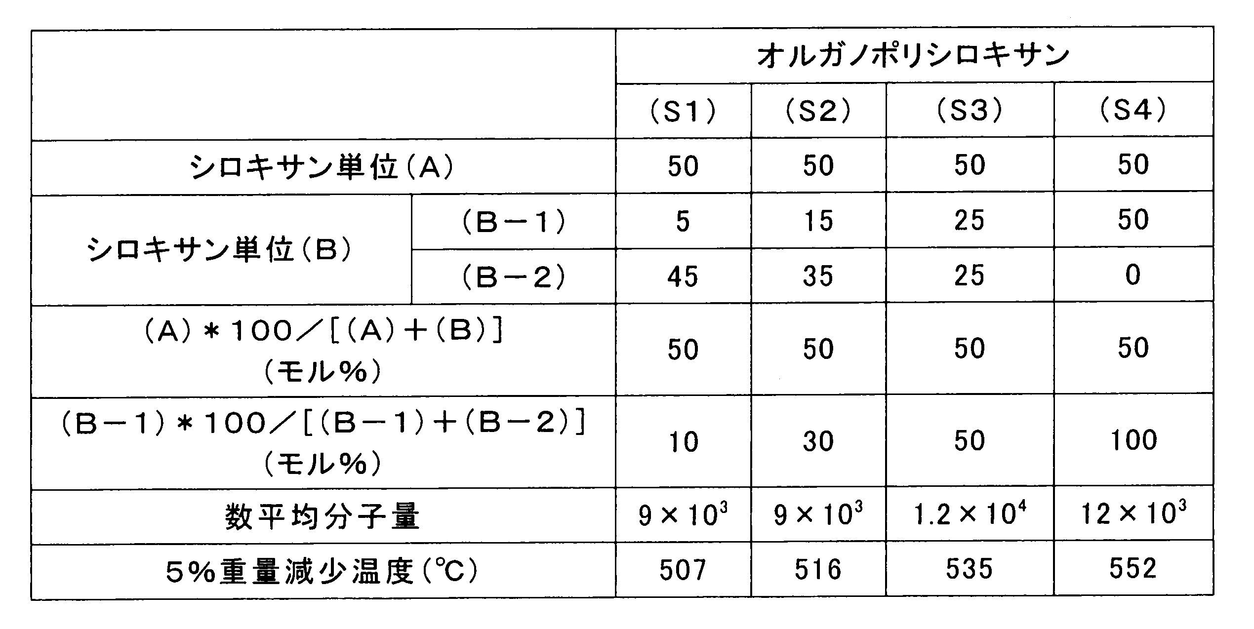
以下の実施例および比較例では、ガラス基板として、無アルカリホウケイ酸ガラスからなるガラス板(縦200mm、横200mm、板厚0.3mm、線膨張係数38×10-7/℃、旭硝子社製商品名「AN100」)を使用した。また、支持基材としては、同じく無アルカリホウケイ酸ガラスからなるガラス板(縦240mm、横240mm、板厚0.4mm、線膨張係数38×10-7/℃、旭硝子社製商品名「AN100」)を使用した。
〈実施例1〉
初めに、板厚0.4mmの支持基材を純水洗浄した後、さらにUV洗浄して清浄化した。
次に、支持基材の第1主面上に、オルガノポリシロキサン(S3)を含むコーティング用組成物を、スピンコータにて塗工した(塗工量120g/m2)。
次に、これを375℃にて30分間大気中で加熱硬化(熱架橋)して、支持基材の第1主面に厚さ6μmのシリコーン樹脂層を形成した。
初めに、板厚0.4mmの支持基材を純水洗浄した後、さらにUV洗浄して清浄化した。
次に、支持基材の第1主面上に、オルガノポリシロキサン(S3)を含むコーティング用組成物を、スピンコータにて塗工した(塗工量120g/m2)。
次に、これを375℃にて30分間大気中で加熱硬化(熱架橋)して、支持基材の第1主面に厚さ6μmのシリコーン樹脂層を形成した。
その後、ガラス基板と、支持基材のシリコーン樹脂層面とを、室温下で真空プレスにより貼り合わせ、ガラス積層体Aを得た。
得られたガラス積層体Aにおいては、支持基材とガラス基板は、シリコーン樹脂層と気泡を発生することなく密着しており、歪み状欠点もなく、平滑性も良好であった。
得られたガラス積層体Aにおいては、支持基材とガラス基板は、シリコーン樹脂層と気泡を発生することなく密着しており、歪み状欠点もなく、平滑性も良好であった。
次に、ガラス積層体Aを大気下で450℃、60分間加熱処理をおこない、室温まで冷却したところ、ガラス積層体Aの支持基材とガラス基板の分離やシリコーン樹脂層の発泡や白化など外観上の変化は認められなかった。
そして、ガラス積層体Aの4箇所のうち1箇所のコーナー部におけるガラス基板とシリコーン樹脂層の界面に厚さ0.1mmのステンレス製刃物を挿入させて剥離の切欠部を形成しながら、ガラス基板と支持基材それぞれの剥離面でない面に真空吸着パッドを吸着させ、互いにガラス基板と支持基材が分離する方向に外力を加えて、ガラス基板と支持基材を破損することなく分離した。ここで刃物の差し込みは、イオナイザ(キーエンス社製)から除電性流体を当該界面に吹き付けながら行った。具体的には、形成した空隙へ向けてイオナイザから引き続き除電性流体を吹き付けながら真空吸着パッドを引き上げた。
なお、シリコーン樹脂層は支持基材と共にガラス基板から分離され、該結果より、支持基材の層とシリコーン樹脂層の界面の剥離強度(x)が、シリコーン樹脂層とガラス基板の界面の剥離強度(y)よりも高いことが確認された。
そして、ガラス積層体Aの4箇所のうち1箇所のコーナー部におけるガラス基板とシリコーン樹脂層の界面に厚さ0.1mmのステンレス製刃物を挿入させて剥離の切欠部を形成しながら、ガラス基板と支持基材それぞれの剥離面でない面に真空吸着パッドを吸着させ、互いにガラス基板と支持基材が分離する方向に外力を加えて、ガラス基板と支持基材を破損することなく分離した。ここで刃物の差し込みは、イオナイザ(キーエンス社製)から除電性流体を当該界面に吹き付けながら行った。具体的には、形成した空隙へ向けてイオナイザから引き続き除電性流体を吹き付けながら真空吸着パッドを引き上げた。
なお、シリコーン樹脂層は支持基材と共にガラス基板から分離され、該結果より、支持基材の層とシリコーン樹脂層の界面の剥離強度(x)が、シリコーン樹脂層とガラス基板の界面の剥離強度(y)よりも高いことが確認された。
〈実施例2〉
実施例1と同様の方法で、支持基材の第1主面上に、オルガノポリシロキサン(S2)の架橋物からなる厚さ6μmのシリコーン樹脂層を形成した。
続いて、実施例1と同様の方法で、ガラス積層体Bを得た。
得られたガラス積層体Bにおいては、支持基材とガラス基板は、シリコーン樹脂層と気泡を発生することなく密着しており、歪み状欠点もなく、平滑性も良好であった。
次に、ガラス積層体Bを実施例1と同様の加熱処理をおこなったところ、ガラス積層体Bの支持基材とガラス基板の分離やシリコーン樹脂層の発泡や白化など外観上の変化は認められなかった。
そして、ガラス積層体Bを実施例1と同様の方法で、ガラス基板と支持基材を破損することなく分離した。シリコーン樹脂層は支持基材と共にガラス基板から分離され、該結果より、支持基材の層とシリコーン樹脂層の界面の剥離強度(x)が、シリコーン樹脂層とガラス基板の界面の剥離強度(y)よりも高いことが確認された。
実施例1と同様の方法で、支持基材の第1主面上に、オルガノポリシロキサン(S2)の架橋物からなる厚さ6μmのシリコーン樹脂層を形成した。
続いて、実施例1と同様の方法で、ガラス積層体Bを得た。
得られたガラス積層体Bにおいては、支持基材とガラス基板は、シリコーン樹脂層と気泡を発生することなく密着しており、歪み状欠点もなく、平滑性も良好であった。
次に、ガラス積層体Bを実施例1と同様の加熱処理をおこなったところ、ガラス積層体Bの支持基材とガラス基板の分離やシリコーン樹脂層の発泡や白化など外観上の変化は認められなかった。
そして、ガラス積層体Bを実施例1と同様の方法で、ガラス基板と支持基材を破損することなく分離した。シリコーン樹脂層は支持基材と共にガラス基板から分離され、該結果より、支持基材の層とシリコーン樹脂層の界面の剥離強度(x)が、シリコーン樹脂層とガラス基板の界面の剥離強度(y)よりも高いことが確認された。
〈比較例1〉
実施例1と同様の方法で、支持基材の第1主面上に、オルガノポリシロキサン(S1)の架橋物からなる厚さ6μmのシリコーン樹脂層を形成した。
続いて、実施例1と同様の方法で、ガラス積層体Oを得た。しかしながら、シリコーン樹脂層は、支持基材およびガラス基板と密着しているものの、粘性液体状のままで固まっておらず、ガラス基板に対する剥離が極めて困難な状態であった。
また、実施例1と同様の加熱処理をおこなったところ、シリコーン樹脂層の発泡が認められた。
実施例1と同様の方法で、支持基材の第1主面上に、オルガノポリシロキサン(S1)の架橋物からなる厚さ6μmのシリコーン樹脂層を形成した。
続いて、実施例1と同様の方法で、ガラス積層体Oを得た。しかしながら、シリコーン樹脂層は、支持基材およびガラス基板と密着しているものの、粘性液体状のままで固まっておらず、ガラス基板に対する剥離が極めて困難な状態であった。
また、実施例1と同様の加熱処理をおこなったところ、シリコーン樹脂層の発泡が認められた。
〈比較例2〉
実施例1と同様の方法で、支持基材の第1主面上に、オルガノポリシロキサン(S4)の架橋物からなる厚さ6μmのシリコーン樹脂層を形成した。
続いて、実施例1と同様の方法で、ガラス積層体Pを得た。しかしながら、得られたガラス積層体Pに対して外力を与えたところシリコーン樹脂層からガラス基板が剥離した。これにより、シリコーン樹脂層のガラス基板に対する密着性が不十分であることがわかった。
また、実施例1と同様の加熱処理をおこなったところ、シリコーン樹脂層の発泡や白化など外観上の変化は認められなかったが、得られたガラス積層体Pに対して外力を与えたところシリコーン樹脂層からガラス基板が剥離した。これにより、加熱処理後においても、シリコーン樹脂層のガラス基板に対する密着性が不十分であることがわかった。
実施例1と同様の方法で、支持基材の第1主面上に、オルガノポリシロキサン(S4)の架橋物からなる厚さ6μmのシリコーン樹脂層を形成した。
続いて、実施例1と同様の方法で、ガラス積層体Pを得た。しかしながら、得られたガラス積層体Pに対して外力を与えたところシリコーン樹脂層からガラス基板が剥離した。これにより、シリコーン樹脂層のガラス基板に対する密着性が不十分であることがわかった。
また、実施例1と同様の加熱処理をおこなったところ、シリコーン樹脂層の発泡や白化など外観上の変化は認められなかったが、得られたガラス積層体Pに対して外力を与えたところシリコーン樹脂層からガラス基板が剥離した。これにより、加熱処理後においても、シリコーン樹脂層のガラス基板に対する密着性が不十分であることがわかった。
〈比較例3〉
支持基材を純水洗浄、UV洗浄等で清浄化した後、該支持基材上に、式(1)で表される単位(A)を含まない無溶剤付加反応型剥離紙用シリコーン(信越シリコーン株式会社製 KNS-320A)100質量部と白金系触媒(信越シリコーン株式会社製 CAT-PL-56)2質量部の混合物をスピンコータにて塗工し(塗工量10g/m2)、180℃にて30分間大気中で加熱硬化して膜厚16μmのシリコーン樹脂層を得た。
ガラス基板のシリコーン樹脂層と接触させる側の面を純水洗浄、UV洗浄等で清浄化した後、支持基材のシリコーン樹脂層形成面と、ガラス基板とを、室温下真空プレスにて貼り合わせ、付加重合型シリコーン樹脂層を有するガラス積層体Qを得た。
次に、ガラス積層体Qを実施例1と同様の加熱処理をおこなったところ、シリコーン樹脂層の発泡、および、白化など外観上の変化が確認された。また、ガラス積層体Q中において、ガラス基板が一部分離した。
支持基材を純水洗浄、UV洗浄等で清浄化した後、該支持基材上に、式(1)で表される単位(A)を含まない無溶剤付加反応型剥離紙用シリコーン(信越シリコーン株式会社製 KNS-320A)100質量部と白金系触媒(信越シリコーン株式会社製 CAT-PL-56)2質量部の混合物をスピンコータにて塗工し(塗工量10g/m2)、180℃にて30分間大気中で加熱硬化して膜厚16μmのシリコーン樹脂層を得た。
ガラス基板のシリコーン樹脂層と接触させる側の面を純水洗浄、UV洗浄等で清浄化した後、支持基材のシリコーン樹脂層形成面と、ガラス基板とを、室温下真空プレスにて貼り合わせ、付加重合型シリコーン樹脂層を有するガラス積層体Qを得た。
次に、ガラス積層体Qを実施例1と同様の加熱処理をおこなったところ、シリコーン樹脂層の発泡、および、白化など外観上の変化が確認された。また、ガラス積層体Q中において、ガラス基板が一部分離した。
本発明を詳細にまた特定の実施態様を参照して説明したが、本発明の精神と範囲を逸脱することなく様々な変更や修正を加えることができることは当業者にとって明らかである。
本出願は、2012年9月27日出願の日本特許出願2012-214061に基づくものであり、その内容はここに参照として取り込まれる。
本出願は、2012年9月27日出願の日本特許出願2012-214061に基づくものであり、その内容はここに参照として取り込まれる。
10 ガラス積層体
12 支持基材(基材)
14 シリコーン樹脂層
14a シリコーン樹脂層の第1主面
16 ガラス基板
16a ガラス基板の第1主面
16b ガラス基板の第2主面
18 シリコーン樹脂層付き基材
20 電子デバイス用部材
22 電子デバイス用部材付き積層体
24 部材付きガラス基板
12 支持基材(基材)
14 シリコーン樹脂層
14a シリコーン樹脂層の第1主面
16 ガラス基板
16a ガラス基板の第1主面
16b ガラス基板の第2主面
18 シリコーン樹脂層付き基材
20 電子デバイス用部材
22 電子デバイス用部材付き積層体
24 部材付きガラス基板
Claims (10)
- 式(1)で表されるシロキサン単位(A)と式(2)で表されるシロキサン単位(B)とを含み、前記シロキサン単位(A)と前記シロキサン単位(B)との合計に対する前記シロキサン単位(A)の割合が30~60モル%であり、全シロキサン単位に対する前記シロキサン単位(A)と前記シロキサン単位(B)との合計の割合が90~100モル%である、オルガノポリシロキサンであって、
前記シロキサン単位(B)が、R5およびR6の少なくとも一方が炭素数3以下のアルケニル基であるシロキサン単位(B-1)、ならびに、R5およびR6のいずれもがそれぞれ炭素数4以下のアルキル基であるシロキサン単位(B-2)からなり、
全前記シロキサン単位(B)に対する前記シロキサン単位(B-1)の割合である[シロキサン単位(B-1)]×100/[シロキサン単位(B-1)+シロキサン単位(B-2)]が25~90モル%である、オルガノポリシロキサン。
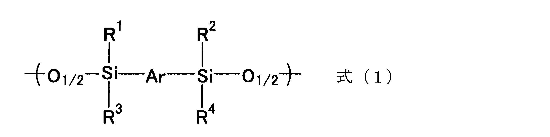
(式(1)中、R1~R4は、それぞれ独立に、炭素数4以下のアルキル基を表し、Arは、置換基を有していてもよいフェニレン基を表す。)

(式(2)中、R5およびR6は、それぞれ独立に、炭素数4以下のアルキル基または炭素数3以下のアルケニル基を表す。) - 前記オルガノポリシロキサンが、前記シロキサン単位(A)と前記シロキサン単位(B)との交互共重合体である、請求項1に記載のオルガノポリシロキサン。
- 前記R1~R4が、いずれもメチル基である、請求項1または2に記載のオルガノポリシロキサン。
- 前記アルケニル基がビニル基である、請求項1~3のいずれか一項に記載のオルガノポリシロキサン。
- 前記シロキサン単位(B-1)が、メチル基およびビニル基を有するシロキサン単位である、請求項1~4のいずれか一項に記載のオルガノポリシロキサン。
- 数平均分子量が、5,000~30,000である、請求項1~5のいずれか一項に記載のオルガノポリシロキサン。
- 式(3)で表されるシラン化合物と式(4)で表されるシラン化合物とを、反応割合がそれぞれ30~60モル%および70~40モル%となるように反応させてオルガノポリシロキサンを製造する方法であって、
該方法が、式(3)で表されるシラン化合物を含む溶液と式(4)で表されるシラン化合物を含む溶液のうちの一方を他方に滴下しながら反応させる方法、または、式(3)で表されるシラン化合物と式(4)で表されるシラン化合物とを溶媒中に同時に添加して反応させる方法であり、
ただし、式(4)で表わされるシラン化合物は、R5およびR6の少なくとも一方が炭素数3以下のアルケニル基であるシラン化合物、ならびに、R5およびR6のいずれもがそれぞれ炭素数4以下のアルキル基であるシラン化合物からなる。

(式(3)中、R1~R4およびArは、式(1)中のR1~R4およびArと同義であり、式(4)中、R5およびR6は、式(2)中のR5およびR6と同義であり、式(3)および式(4)中、XおよびYは、それぞれ独立に、水素原子、ヒドロキシ基または加水分解性基を示す。) - 請求項1~6のいずれか一項に記載のオルガノポリシロキサンを架橋させた架橋物である、架橋オルガノポリシロキサン。
- 前記架橋が熱架橋である、請求項8に記載の架橋オルガノポリシロキサン。
- 請求項1~6のいずれか一項に記載のオルガノポリシロキサンと溶剤とを含む、コーティング用組成物。
Applications Claiming Priority (2)
| Application Number | Priority Date | Filing Date | Title |
|---|---|---|---|
| JP2012-214061 | 2012-09-27 | ||
| JP2012214061A JP2015232053A (ja) | 2012-09-27 | 2012-09-27 | オルガノポリシロキサン、架橋オルガノポリシロキサンおよびコーティング用組成物 |
Publications (1)
| Publication Number | Publication Date |
|---|---|
| WO2014050834A1 true WO2014050834A1 (ja) | 2014-04-03 |
Family
ID=50388231
Family Applications (1)
| Application Number | Title | Priority Date | Filing Date |
|---|---|---|---|
| PCT/JP2013/075766 Ceased WO2014050834A1 (ja) | 2012-09-27 | 2013-09-24 | オルガノポリシロキサン、オルガノポリシロキサンの製造方法、架橋オルガノポリシロキサン、およびコーティング用組成物 |
Country Status (3)
| Country | Link |
|---|---|
| JP (1) | JP2015232053A (ja) |
| TW (1) | TW201420640A (ja) |
| WO (1) | WO2014050834A1 (ja) |
Cited By (3)
| Publication number | Priority date | Publication date | Assignee | Title |
|---|---|---|---|---|
| WO2015156395A1 (ja) * | 2014-04-10 | 2015-10-15 | 旭硝子株式会社 | ガラス積層体およびその製造方法、電子デバイスの製造方法 |
| WO2018105716A1 (ja) * | 2016-12-09 | 2018-06-14 | ダイキン工業株式会社 | ポリマー、組成物及び成形品 |
| US12522714B2 (en) | 2018-10-19 | 2026-01-13 | Merck Patent Gmbh | Polysiloxane composition |
Families Citing this family (2)
| Publication number | Priority date | Publication date | Assignee | Title |
|---|---|---|---|---|
| JP6493268B2 (ja) * | 2016-03-25 | 2019-04-03 | 信越化学工業株式会社 | 主鎖にアリーレン基を有するオルガノポリシロキサンの製造方法 |
| CN113336945B (zh) * | 2021-06-28 | 2023-08-29 | 中国科学院长春应用化学研究所 | 一种主链含亚苯基(苯撑)的硅氧烷聚合物及其制备方法 |
Citations (1)
| Publication number | Priority date | Publication date | Assignee | Title |
|---|---|---|---|---|
| WO2007018028A1 (ja) * | 2005-08-09 | 2007-02-15 | Asahi Glass Company, Limited | 薄板ガラス積層体及び薄板ガラス積層体を用いた表示装置の製造方法 |
-
2012
- 2012-09-27 JP JP2012214061A patent/JP2015232053A/ja active Pending
-
2013
- 2013-09-24 WO PCT/JP2013/075766 patent/WO2014050834A1/ja not_active Ceased
- 2013-09-26 TW TW102134761A patent/TW201420640A/zh unknown
Patent Citations (1)
| Publication number | Priority date | Publication date | Assignee | Title |
|---|---|---|---|---|
| WO2007018028A1 (ja) * | 2005-08-09 | 2007-02-15 | Asahi Glass Company, Limited | 薄板ガラス積層体及び薄板ガラス積層体を用いた表示装置の製造方法 |
Non-Patent Citations (4)
| Title |
|---|
| GADDAM N. BABU ET AL.: "SILARYLENE-SILOXANE POLYMERS: SYNTHESIS, MICROSTRUCTURE AND ADHESIVE PROPERTIES", TECH -TECHNICAL SEMINAR PROCEEDINGS, 2000, pages 47 - 50 * |
| GADDAM N. BABU ET AL.: "Silarylene-Siloxane Polymers: Synthesis, Microstructure and Properties", POLYMER SCIENCE, vol. 1, 1991, pages 53 - 59 * |
| H. DENNIS ZHU ET AL.: "Thermally Stable Silphenylene Vinyl Siloxane Elastomers and Their Blends", MACROMOLECULES, vol. 31, no. 3, 1998, pages 850 - 856 * |
| RICHARD A. NEWMARK ET AL.: "Sequence Analysis of Silarylene-Siloxane Copolymers", MACROMOLECULES, vol. 24, no. 16, 1991, pages 4510 - 4514 * |
Cited By (5)
| Publication number | Priority date | Publication date | Assignee | Title |
|---|---|---|---|---|
| WO2015156395A1 (ja) * | 2014-04-10 | 2015-10-15 | 旭硝子株式会社 | ガラス積層体およびその製造方法、電子デバイスの製造方法 |
| JPWO2015156395A1 (ja) * | 2014-04-10 | 2017-04-13 | 旭硝子株式会社 | ガラス積層体およびその製造方法、電子デバイスの製造方法 |
| WO2018105716A1 (ja) * | 2016-12-09 | 2018-06-14 | ダイキン工業株式会社 | ポリマー、組成物及び成形品 |
| JPWO2018105716A1 (ja) * | 2016-12-09 | 2019-08-08 | ダイキン工業株式会社 | ポリマー、組成物及び成形品 |
| US12522714B2 (en) | 2018-10-19 | 2026-01-13 | Merck Patent Gmbh | Polysiloxane composition |
Also Published As
| Publication number | Publication date |
|---|---|
| JP2015232053A (ja) | 2015-12-24 |
| TW201420640A (zh) | 2014-06-01 |
Similar Documents
| Publication | Publication Date | Title |
|---|---|---|
| JP6555254B2 (ja) | ガラス積層体およびその製造方法、電子デバイスの製造方法 | |
| JP5924344B2 (ja) | 積層体、積層体の製造方法、および、電子デバイス用部材付きガラス基板の製造方法 | |
| TWI641479B (zh) | 玻璃積層體及其製造方法 | |
| CN108248159B (zh) | 层叠体、带有机硅树脂层的支撑基材、带有机硅树脂层的树脂基板、电子器件的制造方法 | |
| JP6610560B2 (ja) | ガラス積層体およびその製造方法、電子デバイスの製造方法 | |
| KR102629661B1 (ko) | 적층체, 실리콘 수지층이 부착된 지지 기재, 실리콘 수지층이 부착된 수지 기판, 및 전자 디바이스의 제조 방법 | |
| JP2017087417A (ja) | ガラス積層体 | |
| WO2017188281A1 (ja) | ガラス積層体およびその製造方法 | |
| WO2014103678A1 (ja) | ガラス積層体およびその製造方法、並びに、シリコーン樹脂層付き支持基材 | |
| KR102526047B1 (ko) | 유리 적층체 및 그의 제조 방법 | |
| JP6194893B2 (ja) | ガラス積層体およびその製造方法、並びに、シリコーン樹脂層付き支持基材 | |
| CN103435257A (zh) | 玻璃膜层叠板及其制造方法 | |
| JP2015232053A (ja) | オルガノポリシロキサン、架橋オルガノポリシロキサンおよびコーティング用組成物 | |
| WO2014050833A1 (ja) | ガラス積層体およびその製造方法、並びに、シリコーン樹脂層付き支持基材およびその製造方法 | |
| JP2018202849A (ja) | 積層体、シリコーン樹脂層付き支持基材、シリコーン樹脂層付き樹脂基板、および、電子デバイスの製造方法 | |
| JP2015182450A (ja) | ガラス積層体 |
Legal Events
| Date | Code | Title | Description |
|---|---|---|---|
| 121 | Ep: the epo has been informed by wipo that ep was designated in this application |
Ref document number: 13841879 Country of ref document: EP Kind code of ref document: A1 |
|
| NENP | Non-entry into the national phase |
Ref country code: DE |
|
| 122 | Ep: pct application non-entry in european phase |
Ref document number: 13841879 Country of ref document: EP Kind code of ref document: A1 |
|
| NENP | Non-entry into the national phase |
Ref country code: JP |