WO2014049852A1 - 光ファイバと接続する光路変換光結合デバイスおよび光モジュール - Google Patents
光ファイバと接続する光路変換光結合デバイスおよび光モジュール Download PDFInfo
- Publication number
- WO2014049852A1 WO2014049852A1 PCT/JP2012/075165 JP2012075165W WO2014049852A1 WO 2014049852 A1 WO2014049852 A1 WO 2014049852A1 JP 2012075165 W JP2012075165 W JP 2012075165W WO 2014049852 A1 WO2014049852 A1 WO 2014049852A1
- Authority
- WO
- WIPO (PCT)
- Prior art keywords
- optical
- optical path
- oblique mirror
- path conversion
- coupling device
- Prior art date
- Legal status (The legal status is an assumption and is not a legal conclusion. Google has not performed a legal analysis and makes no representation as to the accuracy of the status listed.)
- Ceased
Links
Images








Classifications
-
- G—PHYSICS
- G02—OPTICS
- G02B—OPTICAL ELEMENTS, SYSTEMS OR APPARATUS
- G02B6/00—Light guides; Structural details of arrangements comprising light guides and other optical elements, e.g. couplings
- G02B6/24—Coupling light guides
- G02B6/42—Coupling light guides with opto-electronic elements
- G02B6/4201—Packages, e.g. shape, construction, internal or external details
- G02B6/4204—Packages, e.g. shape, construction, internal or external details the coupling comprising intermediate optical elements, e.g. lenses, holograms
- G02B6/4214—Packages, e.g. shape, construction, internal or external details the coupling comprising intermediate optical elements, e.g. lenses, holograms the intermediate optical element having redirecting reflective means, e.g. mirrors, prisms for deflecting the radiation from horizontal to down- or upward direction toward a device
-
- G—PHYSICS
- G02—OPTICS
- G02B—OPTICAL ELEMENTS, SYSTEMS OR APPARATUS
- G02B6/00—Light guides; Structural details of arrangements comprising light guides and other optical elements, e.g. couplings
- G02B6/24—Coupling light guides
- G02B6/42—Coupling light guides with opto-electronic elements
- G02B6/4201—Packages, e.g. shape, construction, internal or external details
- G02B6/4204—Packages, e.g. shape, construction, internal or external details the coupling comprising intermediate optical elements, e.g. lenses, holograms
- G02B6/4212—Packages, e.g. shape, construction, internal or external details the coupling comprising intermediate optical elements, e.g. lenses, holograms the intermediate optical element being a coupling medium interposed therebetween, e.g. epoxy resin, refractive index matching material, index grease, matching liquid or gel
-
- G—PHYSICS
- G02—OPTICS
- G02B—OPTICAL ELEMENTS, SYSTEMS OR APPARATUS
- G02B6/00—Light guides; Structural details of arrangements comprising light guides and other optical elements, e.g. couplings
- G02B6/02—Optical fibres with cladding with or without a coating
- G02B6/02042—Multicore optical fibres
-
- G—PHYSICS
- G02—OPTICS
- G02B—OPTICAL ELEMENTS, SYSTEMS OR APPARATUS
- G02B6/00—Light guides; Structural details of arrangements comprising light guides and other optical elements, e.g. couplings
- G02B6/24—Coupling light guides
- G02B6/42—Coupling light guides with opto-electronic elements
- G02B6/4201—Packages, e.g. shape, construction, internal or external details
- G02B6/4249—Packages, e.g. shape, construction, internal or external details comprising arrays of active devices and fibres
Definitions
- the present invention relates to an optical path conversion optical coupling device connected to an optical fiber, and an optical module.
- optical fiber networks have been developed that exchange large volumes of data at high speeds over relatively long distances of several kilometers or more, such as trunk, metro, and access systems.
- optical interconnect technology that opticalizes signal wiring between devices (several meters to several hundreds of meters) or within devices (several centimeters to several tens of centimeters) in information communication (ICT) equipment. It is considered effective.
- a multi-core fiber MMF
- a conventional fiber has only one core transmission channel in one fiber.
- a multi-core fiber has a transmission channel with a plurality of cores in one fiber, and is attracting attention as a transmission medium that enables high-capacity and high-density transmission.
- optical communication technology in addition to social infrastructure systems, video devices such as video cameras and consumer devices such as personal computers (PCs) and mobile phones are required to have high definition images. As a result, high-speed and large-capacity video signal transmission between the monitor and the terminal, opticalization of the signal transmission line, and the like are realized. Along with this increase in information capacity, optical communication technology for small size, low cost, high density, and large capacity, and realization of optical interconnect between ICT devices / inside devices and consumer devices Optical devices and module technology are required.
- Patent Document 1 discloses an optical device (optical chip) in which a grating coupler is laid out so as to match the arrangement of the core of the MCF and is connected to a photodiode (PD) or a modulator via a waveguide. .
- PD photodiode
- the conventional configuration requires an optical device with a custom layout in accordance with the arrangement of the core of the MCF for optical connection with the MCF.
- MCF is geometrically developed with 7 cores, 19 cores, etc. in view of the demand for uniform spacing between a plurality of cores due to the problem of crosstalk.
- the arrangements such as the core size and the pitch between the cores have been developed by each engine's own design, and the specifications are not unified. Therefore, a custom layout of optical devices is required for each product type.
- the present invention provides an optical path conversion optical coupling device and an optical module that do not require a custom layout for optical connection between an MCF having a general number of cores (7 cores, 19 cores, etc.) and an optical device (for example, a linear array type). provide.
- an optical path conversion optical coupling device for an optical fiber including a plurality of concentrically arranged cores is provided.
- the optical path conversion optical coupling device includes a plurality of first oblique mirror portions arranged concentrically corresponding to the positions of the plurality of cores, and the plurality of first oblique mirror portions includes the plurality of cores.
- the plurality of optical signals emitted from the light source or incident on the plurality of cores are reflected so that the optical paths of the plurality of optical signals do not cross each other.
- an optical fiber having a plurality of cores arranged concentrically, and a plurality of optical signals emitted from or incident on the plurality of cores of the optical fiber.
- An optical path conversion optical coupling device that converts an optical path and a plurality of elements that receive the plurality of optical signals from the optical path conversion optical coupling device or emit the plurality of optical signals to the optical path conversion optical coupling device are arranged linearly
- An optical module is provided.
- the optical path conversion optical coupling device includes a plurality of first oblique mirror portions arranged concentrically corresponding to the positions of the plurality of cores, and the plurality of first oblique mirror portions include: The plurality of optical signals emitted from the plurality of cores or emitted from the array optical element are reflected so that the optical paths of the plurality of optical signals do not cross each other.
- FIG. 1 is an example of an optical module according to the first embodiment of the present invention.
- the optical module 5000 includes a large-capacity optical fiber 1000 represented by a multi-core fiber (hereinafter simply referred to as “optical fiber”) and an optical path conversion unit (optical path conversion optical coupling) disposed inside the optical module 5000.
- Device 100 and an array optical element unit (array optical element) 3000.
- the optical module 5000 is connected to the optical fiber 1000.
- the optical fiber 1000 is disposed on the plane 5001 of the optical module 5000.
- the optical path conversion unit 100 includes a plurality of first oblique mirror units 110-1,..., 110-7.
- the optical path conversion unit 100, the optical fiber 1000, and the array optical element unit 3000 will be described in detail with reference to FIGS.
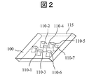
- FIG. 2 is an example of the first optical path conversion unit 100 according to the first embodiment of the present invention.
- 1 and 3 show an optical fiber 1000 having seven core portions 1010-1,..., 1010-7 arranged concentrically as a large capacity optical fiber.
- the optical path conversion unit 100 has a configuration corresponding to the core units 1010-1,..., 1010-7 of the optical fiber 1000.
- the optical path conversion unit 100 includes a plurality of (seven) first oblique mirror units 110-1,..., 110-7, and a second oblique mirror unit 115.
- the plurality of first oblique mirror portions 110-1,..., 110-7 are concentrically arranged corresponding to the positions of the plurality of core portions 1010-1,.
- the optical path conversion unit 100 is preferably made of a material having good transparency with respect to the wavelength of light used for optical communication.
- the optical path conversion unit 100 is realized by glass, resin, a semiconductor such as Si, an organic material, or the like.
- the wavelength is 0.85 ⁇ m
- the optical path conversion unit 100 is realized by glass, resin, organic material, or the like.
- FIG. 2 shows an example in which a plurality of first oblique mirror portions 110-1,..., 110-7 of the optical path changing portion 100 are formed by V-shaped groove-shaped portions.
- V-shaped groove-shaped portions are formed concentrically corresponding to the positions of the plurality of core portions 1010-1, ..., 1010-7.
- one of the two surfaces forming the V-shaped groove-shaped portion is a reflective surface.
- a plurality of optical signals are reflected by the reflecting surfaces of the V-shaped groove-shaped portions of the first oblique mirror portions 110-1,..., 110-7.
- the second oblique mirror unit 115 is configured such that the optical signals reflected by the first oblique mirror units 110-1, ..., 110-7 (or the first oblique mirror parts 110-1, ..., 110-7). Is formed on the surface of the optical path conversion unit 100 corresponding to the optical path of the optical signal reflected toward the.
- the first oblique mirror sections 110-1,..., 110-7 reflect the plurality of optical signals at the same height position so that the optical paths of the plurality of optical signals are parallel to each other.
- the second oblique mirror part 115 is formed as one reflecting surface. As will be described later, the second oblique mirror portion 115 may be formed to have a plurality of reflecting surfaces.
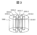
- FIG. 3 shows an example of a large-capacity optical fiber 1000 according to the first embodiment of the present invention.
- the optical fiber 1000 includes a plurality of core portions 1010-1,..., 1010-7 arranged concentrically.
- a plurality of core portions 1010-1,..., 1010-7 extend in the vertical direction.
- This figure shows an example in which the number of cores is 7, but the number of cores may be 19 as will be described later.
- the positional relationship between the core portions 1010-1,..., 1010-7 will be described later in detail with reference to FIG.
- FIG. 4 shows an example of the array optical element unit 3000 according to the first embodiment of the present invention.
- the array optical element unit 3000 can be applied to the present invention in either case of a light receiving element or a light emitting element.
- the array optical element unit 3000 of the present invention includes a plurality of elements (incident part or emitting part) 3010-1,.
- the plurality of elements 3010-1,..., 3010-7 are arranged approximately linearly.
- the array optical element unit 3000 is a general-purpose linear array type optical device.
- the array optical element unit 3000 may be either a light receiving element or a light emitting element.
- the array optical element unit 3000 is a light receiving element
- a plurality of optical signals emitted from the plurality of core units 1010-1,..., 1010-7 are converted in optical path by the optical path conversion unit 100, and the optical path conversion unit 100 Are received by the array optical element unit 3000.
- the array optical element unit 3000 is a light emitting element
- a plurality of optical signals are incident on the optical path conversion unit 100 from the array optical element unit 3000, and the optical path is converted by the optical path conversion unit 100 to obtain an optical path.
- the optical signal from the conversion unit 100 enters the plurality of core units 1010-1,..., 1010-7.
- FIG. 5 shows another example of the optical path changing unit 100 according to the first embodiment of the present invention.
- the example in which the plurality of first oblique mirror portions 110-1,..., 110-7 of the optical path changing portion 100 are formed by V-shaped groove-shaped portions is shown.
- FIG. 5 shows an example in which a plurality of first oblique mirror portions 110-1,..., 110-7 are manufactured by notches.
- a plurality of notches 111-1,..., 111-3 are formed in the optical path conversion unit 100, and each of the surfaces formed by these notches 111-1,.
- the first oblique mirror units 110-1,..., 110-7 are assumed.
- the plurality of first oblique mirror portions 110-1,..., 110-7 correspond to the positions of the plurality of core portions 1010-1,. So that they are arranged concentrically.
- the relative positional relationship between the first oblique mirror portions 110-1,..., 110-7 and the plurality of core portions 1010-1,. is important.
- the plurality of first oblique mirror portions 110-1,..., 110-7 have at least reflecting surfaces arranged concentrically corresponding to the positions of the plurality of core portions 1010-1,. It only has to be. Therefore, the shape of the optical path conversion unit 100 other than the part (reflection surface) where the optical signal is actually reflected by the first oblique mirror units 110-1,..., 110-7 can be arbitrarily formed. .
- resin, low melting glass, etc. are used as a material of the optical path conversion part 100, it can manufacture with a metal mold
- the second oblique mirror unit 115 includes the optical signals reflected by the first oblique mirror units 110-1,..., 110-7 (or the first oblique mirror unit 110- 1,..., 110-7 are formed on the surface of the optical path conversion unit 100 corresponding to the optical path of the optical signal. Since the plurality of first oblique mirror portions 110-1,..., 110-7 and the oblique mirror portion 115 in the optical path changing portion 100 are preferably more efficient in increasing the reflectivity, the first and second oblique mirror portions 110 are used. -1,..., 110-7 and 115 may be coated with a metal (aluminum, gold, etc.) or a dielectric multilayer film. 2 and the optical path conversion unit 100 in FIG. 5 have the same optical path. Therefore, the following description will be made using the optical path conversion unit 100 of FIG. 5 in which the perspective view and the cross-sectional view are simplified.
- FIG. 6 is a top view of the optical module 5000 according to the first embodiment of the present invention.
- an optical signal is sent to each of the core portions 1010-1,..., 1010-7 by making the intervals between the geometrically adjacent core portions 1010-1,. It is preferable to suppress optical crosstalk at the same time during transmission.
- the core portions 1010-1,..., 1010-6 are arranged in a regular hexagon, and the center of the regular hexagon.
- the triangle formed by the three adjacent core portions 1010-2, 1010-3, and 1010-7 is an equilateral triangle, and ⁇ m in FIG. 6 is 60 °.
- the array optical element unit 3000 is a light receiving element
- the optical paths of the plurality of optical signals emitted from the plurality of core units 1010-1,..., 1010-7 are converted by the optical path conversion unit 100, and the plurality of optical signals from the optical path conversion unit 100 are converted into array light. It is received by each element 3010-1,..., 3010-7 of the element unit 3000.
- the angle ⁇ s drawn obliquely is about 20 ° in the case of 7 cores.
- the angle ⁇ s is set to about 20 ° in order to reflect the plurality of optical signals so that the optical paths of the plurality of optical signals are parallel to each other.
- the angle ⁇ s drawn obliquely is not limited to about 20 °, and can be set within an angle range in which the optical paths of the plurality of optical signals do not intersect each other.
- FIG. 7A is a side view showing an optical path conversion unit and an array optical element unit according to the first embodiment of the present invention.
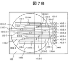
- FIG. 7B is a top view showing the optical path conversion unit and the array optical element unit according to the first embodiment of the present invention.
- the first oblique mirror portions 110-1,..., 110-7 are simply shown as rectangles.
- the optical signals emitted from the plurality of core portions 1010-1,..., 1010-7 of the optical fiber 1000 are sent to the plurality of first lens portions 120- arranged on the upper surface of the optical path changing portion 100. 1,..., 120-7.
- Each of the collected optical signals is reflected by the first oblique mirror units 110-1,..., 110-7 of the optical path conversion unit 100, and is reflected at a right angle so as to have substantially the same height when viewed from the side.
- such optical path conversion is performed by connecting the first oblique mirror portions 110-1,..., 110-7 to the core portions 1010-1,.
- This can be achieved by placing it directly below. That is, as described above, the reflective surfaces of the plurality of first oblique mirror portions 110-1,..., 110-7 are concentric corresponding to the positions of the plurality of core portions 1010-1,. Is arranged.
- the first oblique mirror units 110-1,..., 110-7 receive the plurality of optical signals emitted from the plurality of core units 1010-1,..., 1010-7, and the optical paths 150-1 of the plurality of optical signals. ,..., 150-7 are reflected so as not to cross each other.
- the first oblique mirror sections 110-1,..., 110-7 reflect a plurality of optical signals at the same height when viewed from the side surface and obliquely and substantially parallel when viewed from the upper surface.
- the plurality of optical signals drawn out in this way are reflected downward by the second oblique mirror unit 115 so that the optical paths of the plurality of optical signals are substantially parallel to each other.
- a plurality of optical signals are optically path-converted by a second oblique mirror unit 115 at a right angle substantially below.
- the optical signals collected by the second lens units 130-1,..., 130-7 are converted into the elements 3010-1,..., 3010-7 (in this case, the incident unit) of the array optical element unit 3000. ).
- the above-described optical path is traced in reverse.
- the optical path conversion unit 100 for performing optical coupling between the optical fiber 1000 and the array optical element unit 3000.
- the first oblique mirror sections 110-1,..., 110-7 receive a plurality of optical signals at a substantially right angle at the same height when viewed from the side and a plurality of light when viewed from the top.
- the signal optical paths 150-1,..., 150-7 are reflected so as to be substantially parallel to each other, but the present invention is not limited to such a configuration.
- the positions (heights) of reflection by the first oblique mirror sections 110-1,..., 110-7 may be different, and the optical paths of the plurality of optical signals may be at least not intersecting each other.
- the optical signal reflected by the second oblique mirror unit 115 may be incident on each of the elements 3010-1,..., 3010-7 of the array optical element unit 3000, and the first oblique mirror unit 110.
- the second oblique mirror unit 115 may be configured by a plurality of reflecting surfaces having different heights and angles in accordance with the reflection position (height) and the reflection direction of ⁇ 1,. In this embodiment, since the plurality of optical signals are reflected at the same height when viewed from the side and the optical paths of the plurality of optical signals are substantially parallel to each other, the second oblique mirror unit 115 is reflected. Can be formed as one reflecting surface.
- Patent Document 1 does not use a general-purpose MCF in which cores are concentrically arranged, and the optical fiber itself is inclined on the optical path conversion device. Is required. Therefore, in the technique of Patent Document 1, the optical module also has a large and costly structure.
- Patent Document 1 it is difficult to align the optical fiber because the optical fiber itself is inclined and disposed on the optical path conversion device.
- the optical fiber 1000 is placed on the plane 5001 of the optical module 5000. Since the optical fiber can be aligned while the optical fiber 1000 is placed on the flat surface 5001, there is an advantage that the alignment of the optical fiber is easier than in the prior art.
- the pitch interval of each element (incident part or outgoing part) 3010-1,..., 3010-7 of the array optical element part 3000 is oblique from the core parts 1010-1,.
- the pitch interval of the optical path of the optical signal is widened when the interval between the light beams drawn out is wider.
- this embodiment will be described with reference to FIGS. 8A to 10.
- the case where the array optical element unit 3000 is a light receiving element will be described as an example.
- FIG. 8A is a side view of the optical path conversion unit and the array optical element unit according to the second embodiment.
- FIG. 8B is a top view of the optical path conversion unit and the array optical element unit according to the second embodiment.
- the first oblique mirror portions 110-1,..., 110-7 are simply shown as rectangles.
- the pitch interval of each element (here, the incident part) 3010-1,..., 3010-7 of the array optical element part 3000 is obliquely inclined from the core parts 1010-1,. It is wider than the interval between the optical paths 150-1,.
- the optical path conversion unit 100 includes a second optical path conversion unit 200.
- the second optical path conversion unit 200 changes the optical path interval of the plurality of optical signals reflected by the second oblique mirror unit 115, and converts the plurality of optical signals into each element 3010-1, ..., 3010-7.
- the optical signals emitted from the plurality of core portions 1010-1,..., 1010-7 of the optical fiber 1000 are a plurality of first lens portions 120-1,. , 110-7, and then reflected by the first oblique mirror unit 110-1,..., 110-7, and further reflected downward by the second oblique mirror unit 115, as in the first embodiment. Therefore, the description is omitted.
- a configuration in which the second optical path conversion unit 200 changes the pitch interval of the optical path of the optical signal will be described with reference to FIG.
- FIG. 9 is a cross-sectional view showing the second optical path conversion unit.
- the second optical path conversion unit 200 includes a concave lens unit 200-1, a convex lens unit 200-3, and a lens unit 230.
- the concave lens part 200-1 and the convex lens part 200-3 are supported by a frame body 200a.
- the focal position of the convex lens portion 200-3 and the focal position of the concave lens portion 200-1 are made the same (focal point 300).
- the condensing lens unit 230 includes a plurality of lens units 230-1, ..., 230-7.
- optical signal that has fallen substantially parallel and directly below by the second oblique mirror unit 115 of the optical path conversion unit 100 travels so as to spread by the concave lens unit 200-1.
- these optical signals are narrowed by the convex lens unit 200-3, but the focal position of the convex lens unit 200-3 and the focal position of the concave lens unit 200-1 are the same (focal point 300).
- the emitted optical signal travels substantially parallel and directly below.
- the optical signal that has passed through the convex lens part 200-3 is stopped by the lens parts 230-1,..., 230-7, and is incident on the elements 3010-1,..., 3010-7 of the array optical element part 3000.
- the array optical element unit 3000 is a light-emitting element, the above-described optical path is traced in reverse.
- the concave lens unit 200-1 and the convex lens unit 200-3 may use cylindrical lenses.
- FIG. 10 is a cross-sectional view of another example of the second optical path changing unit according to the second embodiment of the present invention.
- the second optical path conversion unit 210 in this example includes a first prism unit 210-1 having a polygonal shape and a second prism unit 220-3 having a polygonal shape.
- the first prism unit 210-1 widens the optical path intervals of the plurality of optical signals
- the second prism unit 220-3 makes the optical paths of the plurality of optical signals substantially parallel to each other. That is, as shown in FIG. 10, the optical signal that has fallen substantially parallel and directly below by the second oblique mirror unit 115 of the optical path conversion unit 100 travels so as to spread by the first prism unit 210-1.
- the optical signal travels substantially parallel and directly below by the second prism portion 220-3.
- the beam of the optical signal itself is spread by the lens. It becomes possible to eliminate the influence of narrowing or narrowing.
- the second optical path conversion unit 200 may be configured with another member such as a diffraction grating or a mirror as long as the optical path of the optical signal is widened and then traveled approximately in parallel.
- the concave lens portion 200-1 and the convex lens portion 200-3 are supported by the frame body 200a.
- a part of the optical path conversion unit 100 is cut out without using the frame body 200a. It is also possible to integrally form the second optical path conversion units 200, 210 and the like.
- the pitch interval of each element (incident part or outgoing part) 3010-1,..., 3010-7 of the array optical element part 3000 is oblique from the core parts 1010-1,. Even when the distance between the optical paths 150-1,..., 150-7 of the optical signal drawn out to the optical signal is wider, the optical fiber 1000 and the array optical element unit 3000 can be optically coupled.
- the angles of the reflection surfaces of the plurality of first oblique mirror portions 110-1,..., 110-7 are the same, and the second oblique mirror portion 115 is also configured as one reflection surface. Therefore, there is an advantage that the configuration of the first oblique mirror unit 110-1,..., 110-7 and the second oblique mirror unit 115 is simplified.
- FIG. 11 is a top view of an optical module that is a third embodiment of the present invention and that is applied to a large-capacity optical fiber 1000 when the number of cores is 19.
- the spacing between the geometrically adjacent core portions 1020-1,..., 1020-19 is made uniform, and the optical signal is transmitted through the core portions 1020-1,. It is preferable to equally suppress optical crosstalk during transmission.
- 6 core portions are arranged in a regular hexagon, and a regular length equal to the length of the side of the regular hexagon. Twelve core parts are arranged on the dodecagon, and the core parts 1020-19 are arranged so that the centers of the regular hexagon and the regular dodecagon are at the same position.
- the distance between the core part 1020-19 and the core part 1020-13 and the distance between the core part 1020-13 and the core part 1020-1 are equal to the length of the side of the regular hexagon (on the regular dodecagon). Deploy. Since the triangle formed by the three adjacent core portions is a regular triangle, ⁇ m in FIG. 11 is 60 °.
- the other core portions are avoided and the linear optical signal is drawn obliquely.
- the angle ⁇ s drawn obliquely is about 12 ° in the case of 19 cores.
- the 19 first oblique mirror portions are arranged concentrically corresponding to the positions of the 19 core portions 1020-1,..., 1020-19.
- the nineteen first oblique mirror portions reflect the plurality of optical signals so that the optical paths of the plurality of optical signals are substantially parallel to each other, but the angle ⁇ s is about 12 °.
- the angle ⁇ s drawn obliquely is not limited to about 12 °, and can be set within an angle range such that the optical paths of a plurality of optical signals do not intersect each other.
- the angle ⁇ s that is drawn obliquely from the central axis of the large-capacity optical fiber 1000 as viewed from above is set according to the number of cores, and the optical paths of a plurality of optical signals are drawn out so as not to cross each other. Thereby, the optical coupling between the large-capacity optical fiber 1000 and the array optical element unit 3000 when the number of cores is 19 becomes possible.
- the pitch interval of each element (incident part or outgoing part) 3010-1,..., 3010-7 of the array optical element part 3000 is oblique from the core parts 1010-1,.
- Another embodiment is shown in which the pitch interval of the optical path of the optical signal is increased when the interval of the optical path of the optical signal drawn out is wider.
- the array optical element unit 3000 is a light receiving element will be described as an example.
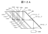
- FIG. 12A is a side view of the optical path conversion unit and the array optical element unit according to the fourth embodiment.
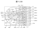
- FIG. 12B is a top view of the optical path conversion unit and the array optical element unit according to the fourth embodiment.
- the optical path conversion unit 100 corresponds to a plurality of first oblique mirror units 110-1,..., 110-7 and a plurality of first oblique mirror units 110-1,.
- the optical signals are not drawn obliquely and approximately in parallel from the optical fiber 1000 when viewed from above, and a plurality of second mirrors that are paired with the first oblique mirror portions 110-1,. , 115-7 so that optical signals are incident on the elements (in this case, incident portions) 3010-1,..., 3010-7 of the array optical element unit 3000. is there.
- a plurality of second oblique mirror sections 115-1,..., 115-7 are arranged in parallel corresponding to the positions of the respective elements 3010-1, ..., 3010-7 of the array optical element section 3000. Is arranged.
- the optical signal emitted from the optical fiber 1000 is collected by the plurality of first lens units 120-1,..., 120-7 disposed on the upper surface of the optical path conversion unit 100 and enters the optical path conversion unit 100.
- This optical signal is reflected by the first oblique mirror units 110-1,..., 110-7 of the optical path conversion unit 100, and is reflected so as to have substantially the same height when viewed from the side.
- such optical path conversion is performed by the first oblique mirror portions 110-1,..., 110- approximately below the core portions 1010-1,. This can be realized by arranging 7.
- each of the plurality of first oblique mirror portions 110-1,..., 110-7 has a different angle when viewed from the top.
- the first oblique mirror unit 110-7 includes the second oblique mirror unit 115-7 at the center of the second oblique mirror units 115-1,.
- the angle at which the optical signal is extracted obliquely is set smaller than the others.
- the first oblique mirror unit 110-4 reflects toward the outermost second oblique mirror unit 115-4 among the second oblique mirror units 115-1, ..., 115-7.
- the angle at which the optical signal is extracted obliquely is set to be larger than that in the case of the first oblique mirror unit 110-7.
- the reflection surfaces of the plurality of first oblique mirror portions 110-1,..., 110-7 are respectively matched with the positions of the corresponding second oblique mirror portions 115-1,. Set the angle.
- the plurality of first oblique mirror portions 110-1,..., 110-7 widen the intervals of the optical paths 150-1,.
- the light can be reflected toward the plurality of second oblique mirror portions 115-1,..., 115-7.
- the plurality of first oblique mirror portions 110-1,..., 110-7 are reflected at the same height when viewed from the side.
- the optical signals drawn out in the same height as viewed from the side and extending in the direction viewed from the upper surface are optically path-converted almost directly by the plurality of second oblique mirror portions 115-1,..., 115-7. That is, the plurality of second oblique mirror units 115-1,..., 115-7 receive the plurality of optical signals reflected by the plurality of first oblique mirror units 110-1,.
- the optical signals are reflected so that their optical paths are parallel to each other, and are incident on each element of the array optical element.
- Such optical path conversion can be realized by giving different angles to the reflecting surfaces of the plurality of second oblique mirror portions 115-1,..., 115-7 when viewed from above.
- the optical signals reflected by the plurality of second oblique mirror portions 115-1,..., 115-7 are collected by the second lens portions 130-1,. It enters each element 3010-1,..., 3010-7.
- the array optical element unit 3000 is a light-emitting element, the above-described optical path is traced in reverse.
- the pitch interval of each element (incident part or outgoing part) 3010-1,..., 3010-7 of the array optical element part 3000 is oblique from the core parts 1010-1,.
- the optical fiber 1000 and the array optical element can be used without using another member such as the concave lens portion 200-1 and the convex lens portion 200-3 as in the second embodiment.
- Optical coupling with the unit 3000 is possible. For example, when the distance of the optical path of the optical signal is increased using another member, it is necessary to consider the influence of the coefficient of thermal expansion for each material. However, in this embodiment, it is not necessary to consider such influence.
- FIG. 13A is a side view of the optical path conversion unit and the array optical element unit according to the fifth embodiment.
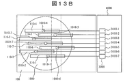
- FIG. 13B is a top view of the optical path conversion unit and the array optical element unit according to the fifth embodiment. In the top view of FIG. 13B, the first oblique mirror portions 110-1,..., 110-7 are simply shown as rectangles.
- the optical signals emitted from the respective elements (here, the emitting units) 3010-1,..., 3010-7 of the array optical element unit 3000 are converted into the second lens units 130-1,.
- the light is collected by and travels in the horizontal direction when viewed from the side.
- the plurality of optical signals are reflected by the plurality of first oblique mirror portions 110-1,..., 110-7.
- the plurality of optical signals reflected by the plurality of first oblique mirror sections 110-1,..., 110-7 travel so that they are substantially directly above and the optical paths of the plurality of optical signals are substantially parallel to each other.
- the plurality of optical signals are collected by the plurality of first lens portions 120-1,..., 120-7, and are incident on the plurality of core portions 1010-1,. .
- the optical fiber 1000 and the array optical element unit 3000 can be optically coupled even when each element 3010-1,..., 3010-7 of the array optical element unit 3000 is the incident part of the edge emitter. become.
- FIG. 14A is a side view of the optical path conversion unit and the array optical element unit according to the sixth embodiment.
- FIG. 14B is a top view of the optical path conversion unit and the array optical element unit according to the sixth embodiment.
- the first oblique mirror portions 110-1,..., 110-7 are simply shown as rectangles.
- the case where the array optical element unit 3000 is a light receiving element will be described as an example.
- the second oblique mirror unit 115 of the optical path conversion unit 100 includes an optical path branching unit 117 that branches a plurality of optical signals in two directions.
- an optical signal is branched into two, one optical signal is incident on the array optical element portion 3000 as a main signal, and the other optical signal is, for example, optical It is processed as a monitor signal such as power.
- a partial transmission mirror with the transmittance changed as appropriate can be used. Thereby, it is possible to transmit the optical signal as it is and to go straight while reflecting the optical signal.
- the optical path branching unit 117 only needs to be able to branch an optical signal in two directions, and may be realized by another configuration such as using a mirror.
- the optical signal emitted from the optical fiber 1000 is collected by the first lens units 120-1,..., 120-7 disposed on the upper surface of the optical path conversion unit 100 and enters the optical path conversion unit 100.
- This optical signal is reflected by the plurality of first oblique mirror units 110-1,..., 110-7 of the optical path conversion unit 100, and is reflected at a right angle so as to have substantially the same height when viewed from the side.
- such optical path conversion is performed by a plurality of first oblique mirror portions 110-1,..., Approximately directly below each core portion 1010-1,. This can be realized by arranging 110-7.
- the optical signal with the same height when viewed from the side and withdrawn substantially in parallel obliquely when viewed from the upper surface is branched by the optical path branching portion 117 of the second oblique mirror portion 115.
- One of the branched optical signals enters the array optical element unit 3000 as a main signal, and the other optical signal proceeds in the horizontal direction as it is, and can be processed as a monitoring signal such as optical power. Become.
- this invention is not limited to the above-mentioned Example, Various modifications are included.
- the above-described embodiments have been described in detail for easy understanding of the present invention, and are not necessarily limited to those having all the configurations described.
- a part of the configuration of one embodiment can be replaced with the configuration of another embodiment, and the configuration of another embodiment can be added to the configuration of one embodiment.
- optical path conversion unit 110-1,..., 110-7 first oblique mirror unit 111-1,..., 111-3: notch 115: second oblique mirror unit 115-1,. 7: second oblique mirror unit 117: optical path branching unit 200: second optical path conversion unit 210: second optical path conversion unit 1000: large capacity optical fiber 1010-1, ..., 1010-7: core unit 1020-1 ,..., 1020-19: Core part 3000: Array optical element part 3010-1,..., 3010-7: Element 5000: Optical module
Landscapes
- Physics & Mathematics (AREA)
- General Physics & Mathematics (AREA)
- Optics & Photonics (AREA)
- Optical Couplings Of Light Guides (AREA)
Description
本実施例では、マルチコアファイバ(MCF)である光ファイバと、直線アレイ型のアレイ光素子との光接続を実現する光路変換光結合デバイスの例を説明する。さらに、本実施例では、当該光ファイバとアレイ光素子と光路変換光結合デバイスとを備える光モジュールの例を説明する。
本実施例では、アレイ光素子部3000の各素子(入射部あるいは出射部)3010-1,…,3010-7のピッチ間隔が光ファイバ1000のコア部1010-1,…,1010-7から斜めに引き出した光線の間隔よりも広い場合に、光信号の光路のピッチ間隔を広げる実施例を示している。以下では、本実施例を図8A~図10を用いて説明する。ここでは、アレイ光素子部3000が受光素子の場合を例として説明する。
図11は、本発明の第3の実施例であり、コア数が19の場合の大容量光ファイバ1000に適用する光モジュールの上面図である。
本実施例では、アレイ光素子部3000の各素子(入射部あるいは出射部)3010-1,…,3010-7のピッチ間隔が光ファイバ1000のコア部1010-1,…,1010-7から斜めに引き出した光信号の光路の間隔よりも広い場合に、光信号の光路のピッチ間隔を広げる別の実施例を示している。ここでは、アレイ光素子部3000が受光素子の場合を例として説明する。
本実施例では、ここでは、アレイ光素子部3000が発光素子の場合を例として説明する。例えば、アレイ光素子部3000は、基板4000上に半田などを介して接合されているエッジエミッタである。図13Aは、第5実施例に係る光路変換部とアレイ光素子部の側面図である。また、図13Bは、第5実施例に係る光路変換部とアレイ光素子部の上面図である。なお、図13Bの上面図において、第1の斜めミラー部110-1,…,110-7は、長方形で簡略的に示されている。
図14Aは、第6実施例に係る光路変換部とアレイ光素子部の側面図である。また、図14Bは、第6実施例に係る光路変換部とアレイ光素子部の上面図である。なお、図14Bの上面図において、第1の斜めミラー部110-1,…,110-7は、長方形で簡略的に示されている。ここでは、アレイ光素子部3000が受光素子の場合を例として説明する。
110-1,…,110-7 :第1の斜めミラー部
111-1,…,111-3 :切り欠き部
115 :第2の斜めミラー部
115-1,…,115-7 :第2の斜めミラー部
117 :光路分岐部
200 :第2の光路変換部
210 :第2の光路変換部
1000 :大容量光ファイバ
1010-1,…,1010-7 :コア部
1020-1,…,1020-19 :コア部
3000 :アレイ光素子部
3010-1,…,3010-7 :素子
5000 :光モジュール
Claims (14)
- 同心状に配置された複数のコアを備える光ファイバ用の光路変換光結合デバイスであって、
前記複数のコアの位置に対応して同心状に配置された複数の第1の斜めミラー部を備え、
前記複数の第1の斜めミラー部は、前記複数のコアから出射される、あるいは前記複数のコアに入射する複数の光信号を、当該複数の光信号の光路が互いに交差しないように反射させることを特徴とする光路変換光結合デバイス。 - 請求項1に記載の光路変換光結合デバイスにおいて、
前記複数の第1の斜めミラー部で反射された複数の光信号を反射させる1つ以上の第2の斜めミラー部を更に備えることを特徴とする光路変換光結合デバイス。 - 請求項2に記載の光路変換光結合デバイスにおいて、
前記第2の斜めミラー部で反射された前記複数の光信号の光路間隔を変更する光路変換部を更に備えることを特徴とする光路変換光結合デバイス。 - 請求項3に記載の光路変換光結合デバイスにおいて、
前記光路変換部が、凹レンズと凸レンズとを備え、前記凹レンズの焦点の位置及び前記凸レンズの焦点の位置が同じであることを特徴とする光路変換光結合デバイス。 - 請求項3に記載の光路変換光結合デバイスにおいて、
前記光路変換部が、前記複数の光信号の光路間隔を広げる第1の多角形プリズムと、前記複数の光信号の光路を互いに平行にする第2の多角形プリズムとを備えることを特徴とする光路変換光結合デバイス。 - 請求項2に記載の光路変換光結合デバイスにおいて、
複数の第2の斜めミラー部が、並列に配置されており、
前記複数の第1の斜めミラー部は、前記複数の光信号を、前記並列に配置された前記複数の第2の斜めミラー部に向かって反射させ、
前記第2の斜めミラー部は、前記複数の第1の斜めミラー部で反射された複数の光信号を、前記複数の光信号の光路が互いに平行になるように反射させることを特徴とする光路変換光結合デバイス。 - 請求項2に記載の光路変換光結合デバイスにおいて、
前記第2の斜めミラー部は、前記複数の光信号を2つの方向に分岐させる光路分岐部を備えることを特徴とする光路変換光結合デバイス。 - 同心状に配置された複数のコアを備える光ファイバと、
前記光ファイバの前記複数のコアから出射される、あるいは前記複数のコアに入射する複数の光信号の光路を変換する光路変換光結合デバイスと、
前記複数の光信号を前記光路変換光結合デバイスから受ける、あるいは前記複数の光信号を前記光路変換光結合デバイスへ出射させる複数の素子が直線状に配置されたアレイ光素子と、
を備え、
前記光路変換光結合デバイスは、前記複数のコアの位置に対応して同心状に配置された複数の第1の斜めミラー部を備え、
前記複数の第1の斜めミラー部は、前記複数のコアから出射される、あるいは前記アレイ光素子から出射される前記複数の光信号を、当該複数の光信号の光路が互いに交差しないように反射させることを特徴とする光モジュール。 - 請求項8に記載の光モジュールにおいて、
前記光路変換光結合デバイスは、前記複数の第1の斜めミラー部で反射された前記複数の光信号を反射させて、前記複数の光信号を前記アレイ光素子の各素子に入射させる1つ以上の第2の斜めミラー部を更に備えることを特徴とする光モジュール。 - 請求項9に記載の光モジュールにおいて、
前記光路変換光結合デバイスは、前記第2の斜めミラー部で反射された前記複数の光信号の光路間隔を変更して、前記複数の光信号を前記アレイ光素子の各素子に入射させる光路変換部を更に備えることを特徴とする光モジュール。 - 請求項10に記載の光モジュールにおいて、
前記光路変換部が、凹レンズと凸レンズとを備え、前記凹レンズの焦点の位置及び前記凸レンズの焦点の位置が同じであることを特徴とする光モジュール。 - 請求項10に記載の光モジュールにおいて、
前記光路変換部が、前記光路変換部が、前記複数の光信号の光路間隔を広げる第1の多角形プリズムと、前記複数の光信号の光路を互いに平行にする第2の多角形プリズムとを備えることを特徴とする光モジュール。 - 請求項9に記載の光モジュールにおいて、
複数の第2の斜めミラー部が、前記アレイ光素子の各素子の位置に対応して並列に配置されており、
前記複数の第1の斜めミラー部は、前記複数の光信号を、前記並列に配置された前記複数の第2の斜めミラー部に向かって反射させ、
前記第2の斜めミラー部は、前記複数の第1の斜めミラー部で反射された複数の光信号を、前記複数の光信号の光路が互いに平行になるように反射させて、前記アレイ光素子の各素子に入射させることを特徴とする光モジュール。 - 請求項9に記載の光モジュールにおいて、
前記第2の斜めミラー部は、前記複数の光信号を2つの方向に分岐させる光路分岐部を備え、前記光路分岐部によって分岐された一方の光信号が、前記アレイ光素子の各素子に入射することを特徴とする光モジュール。
Priority Applications (3)
| Application Number | Priority Date | Filing Date | Title |
|---|---|---|---|
| JP2014538048A JPWO2014049852A1 (ja) | 2012-09-28 | 2012-09-28 | 光ファイバと接続する光路変換光結合デバイスおよび光モジュール |
| US14/422,816 US20150234134A1 (en) | 2012-09-28 | 2012-09-28 | Optical Path Converting Optical Coupling Device Connected with Optical Fiber, and Optical Module |
| PCT/JP2012/075165 WO2014049852A1 (ja) | 2012-09-28 | 2012-09-28 | 光ファイバと接続する光路変換光結合デバイスおよび光モジュール |
Applications Claiming Priority (1)
| Application Number | Priority Date | Filing Date | Title |
|---|---|---|---|
| PCT/JP2012/075165 WO2014049852A1 (ja) | 2012-09-28 | 2012-09-28 | 光ファイバと接続する光路変換光結合デバイスおよび光モジュール |
Publications (1)
| Publication Number | Publication Date |
|---|---|
| WO2014049852A1 true WO2014049852A1 (ja) | 2014-04-03 |
Family
ID=50387313
Family Applications (1)
| Application Number | Title | Priority Date | Filing Date |
|---|---|---|---|
| PCT/JP2012/075165 Ceased WO2014049852A1 (ja) | 2012-09-28 | 2012-09-28 | 光ファイバと接続する光路変換光結合デバイスおよび光モジュール |
Country Status (3)
| Country | Link |
|---|---|
| US (1) | US20150234134A1 (ja) |
| JP (1) | JPWO2014049852A1 (ja) |
| WO (1) | WO2014049852A1 (ja) |
Cited By (1)
| Publication number | Priority date | Publication date | Assignee | Title |
|---|---|---|---|---|
| WO2022249456A1 (ja) * | 2021-05-28 | 2022-12-01 | 日本電信電話株式会社 | 光モニタデバイス及び光強度測定方法 |
Citations (3)
| Publication number | Priority date | Publication date | Assignee | Title |
|---|---|---|---|---|
| JPH07110443A (ja) * | 1993-10-08 | 1995-04-25 | Hoya Corp | 非球面テレセントリックレンズ |
| JP2003262822A (ja) * | 2002-03-12 | 2003-09-19 | Nippon Telegr & Teleph Corp <Ntt> | 二次元配列された光ビームの配列間隔変換光学系 |
| JP2010286697A (ja) * | 2009-06-12 | 2010-12-24 | Sumitomo Electric Ind Ltd | 光配列変換デバイス |
Family Cites Families (5)
| Publication number | Priority date | Publication date | Assignee | Title |
|---|---|---|---|---|
| JPH02149945A (ja) * | 1988-12-01 | 1990-06-08 | Canon Inc | 光学ヘッド装置 |
| US8804246B2 (en) * | 2008-05-08 | 2014-08-12 | Ii-Vi Laser Enterprise Gmbh | High brightness diode output methods and devices |
| JP5314587B2 (ja) * | 2009-12-21 | 2013-10-16 | パナソニック株式会社 | 光モジュール |
| US20120155805A1 (en) * | 2010-12-20 | 2012-06-21 | Christopher Doerr | Multi-core optical cable to photonic circuit coupler |
| US10078190B2 (en) * | 2010-12-20 | 2018-09-18 | Alcatel Lucent | Multi-core optical cable to photonic circuit coupler |
-
2012
- 2012-09-28 WO PCT/JP2012/075165 patent/WO2014049852A1/ja not_active Ceased
- 2012-09-28 JP JP2014538048A patent/JPWO2014049852A1/ja active Pending
- 2012-09-28 US US14/422,816 patent/US20150234134A1/en not_active Abandoned
Patent Citations (3)
| Publication number | Priority date | Publication date | Assignee | Title |
|---|---|---|---|---|
| JPH07110443A (ja) * | 1993-10-08 | 1995-04-25 | Hoya Corp | 非球面テレセントリックレンズ |
| JP2003262822A (ja) * | 2002-03-12 | 2003-09-19 | Nippon Telegr & Teleph Corp <Ntt> | 二次元配列された光ビームの配列間隔変換光学系 |
| JP2010286697A (ja) * | 2009-06-12 | 2010-12-24 | Sumitomo Electric Ind Ltd | 光配列変換デバイス |
Cited By (3)
| Publication number | Priority date | Publication date | Assignee | Title |
|---|---|---|---|---|
| WO2022249456A1 (ja) * | 2021-05-28 | 2022-12-01 | 日本電信電話株式会社 | 光モニタデバイス及び光強度測定方法 |
| JPWO2022249456A1 (ja) * | 2021-05-28 | 2022-12-01 | ||
| JP7609268B2 (ja) | 2021-05-28 | 2025-01-07 | 日本電信電話株式会社 | 光モニタデバイス及び光強度測定方法 |
Also Published As
| Publication number | Publication date |
|---|---|
| US20150234134A1 (en) | 2015-08-20 |
| JPWO2014049852A1 (ja) | 2016-08-22 |
Similar Documents
| Publication | Publication Date | Title |
|---|---|---|
| US9322987B2 (en) | Multicore fiber coupler between multicore fibers and optical waveguides | |
| JP5445579B2 (ja) | 光導波路モジュール | |
| US9778420B2 (en) | Connecting structure of optical module and optical connector | |
| US9086551B2 (en) | Double mirror structure for wavelength division multiplexing with polymer waveguides | |
| US11287577B2 (en) | Optical mode converter for coupling between waveguides with different mode size | |
| JP2007264033A (ja) | 光モジュール、光伝送システム、光モジュールの製造方法 | |
| US20050175306A1 (en) | Waveguides with integrated lenses and reflective surfaces | |
| US12055772B2 (en) | Optical interconnect and method of manufacture thereof | |
| JP2015537257A (ja) | カップリングレンズを備えたマルチチャネル光コネクタ | |
| CN110989088A (zh) | 一种基于透镜和超表面透镜的复用/解复用装置及方法 | |
| CN104422990A (zh) | 利用多芯光纤进行波分解复用的方法和光学系统 | |
| JP5446492B2 (ja) | 光配列変換デバイス | |
| WO2014049852A1 (ja) | 光ファイバと接続する光路変換光結合デバイスおよび光モジュール | |
| JP4511291B2 (ja) | 光接続装置の製造法及びその光接続装置 | |
| JP2013012548A (ja) | 光モジュールおよび光電気混載ボード | |
| CN110989079B (zh) | 一种空气包层su8阵列波导光栅 | |
| KR102734233B1 (ko) | 양방향 연마된 실리카 광 도파로를 이용하는 광 모듈 패키지 | |
| CN117270101A (zh) | 一种粗波分复用器/解复用器和光子集成芯片 | |
| KR101630354B1 (ko) | 양방향 광 송수신 모듈 | |
| JP6411899B2 (ja) | マルチコアファイバ接続装置およびシステム | |
| US20210063653A1 (en) | Optical module and optical communication network system having the same | |
| US20250264660A1 (en) | Offloading photonic integrated circuit functionality into optical interconnects | |
| CN204903820U (zh) | 基片、大单元激光器阵列及阵列模块、光探测器阵列及阵列模块、光纤发射及接收模块 | |
| JP5898732B2 (ja) | 光モジュールの製造方法 | |
| CN115951452B (zh) | 一种基于多相位面的多模波导耦合器 |
Legal Events
| Date | Code | Title | Description |
|---|---|---|---|
| 121 | Ep: the epo has been informed by wipo that ep was designated in this application |
Ref document number: 12885718 Country of ref document: EP Kind code of ref document: A1 |
|
| ENP | Entry into the national phase |
Ref document number: 2014538048 Country of ref document: JP Kind code of ref document: A |
|
| WWE | Wipo information: entry into national phase |
Ref document number: 14422816 Country of ref document: US |
|
| NENP | Non-entry into the national phase |
Ref country code: DE |
|
| 122 | Ep: pct application non-entry in european phase |
Ref document number: 12885718 Country of ref document: EP Kind code of ref document: A1 |