WO2014046151A1 - 濾過用フィルタの製造方法 - Google Patents
濾過用フィルタの製造方法 Download PDFInfo
- Publication number
- WO2014046151A1 WO2014046151A1 PCT/JP2013/075213 JP2013075213W WO2014046151A1 WO 2014046151 A1 WO2014046151 A1 WO 2014046151A1 JP 2013075213 W JP2013075213 W JP 2013075213W WO 2014046151 A1 WO2014046151 A1 WO 2014046151A1
- Authority
- WO
- WIPO (PCT)
- Prior art keywords
- film
- filtration
- substrate
- flow path
- sacrificial film
- Prior art date
- Legal status (The legal status is an assumption and is not a legal conclusion. Google has not performed a legal analysis and makes no representation as to the accuracy of the status listed.)
- Ceased
Links
Images








Classifications
-
- B—PERFORMING OPERATIONS; TRANSPORTING
- B01—PHYSICAL OR CHEMICAL PROCESSES OR APPARATUS IN GENERAL
- B01D—SEPARATION
- B01D67/00—Processes specially adapted for manufacturing semi-permeable membranes for separation processes or apparatus
- B01D67/0002—Organic membrane manufacture
- B01D67/0023—Organic membrane manufacture by inducing porosity into non porous precursor membranes
- B01D67/0032—Organic membrane manufacture by inducing porosity into non porous precursor membranes by elimination of segments of the precursor, e.g. nucleation-track membranes, lithography or laser methods
- B01D67/0034—Organic membrane manufacture by inducing porosity into non porous precursor membranes by elimination of segments of the precursor, e.g. nucleation-track membranes, lithography or laser methods by micromachining techniques, e.g. using masking and etching steps, photolithography
-
- B—PERFORMING OPERATIONS; TRANSPORTING
- B01—PHYSICAL OR CHEMICAL PROCESSES OR APPARATUS IN GENERAL
- B01D—SEPARATION
- B01D61/00—Processes of separation using semi-permeable membranes, e.g. dialysis, osmosis or ultrafiltration; Apparatus, accessories or auxiliary operations specially adapted therefor
- B01D61/02—Reverse osmosis; Hyperfiltration ; Nanofiltration
- B01D61/08—Apparatus therefor
-
- B—PERFORMING OPERATIONS; TRANSPORTING
- B01—PHYSICAL OR CHEMICAL PROCESSES OR APPARATUS IN GENERAL
- B01D—SEPARATION
- B01D63/00—Apparatus in general for separation processes using semi-permeable membranes
- B01D63/08—Flat membrane modules
- B01D63/081—Manufacturing thereof
-
- B—PERFORMING OPERATIONS; TRANSPORTING
- B01—PHYSICAL OR CHEMICAL PROCESSES OR APPARATUS IN GENERAL
- B01D—SEPARATION
- B01D63/00—Apparatus in general for separation processes using semi-permeable membranes
- B01D63/08—Flat membrane modules
- B01D63/087—Single membrane modules
-
- B—PERFORMING OPERATIONS; TRANSPORTING
- B01—PHYSICAL OR CHEMICAL PROCESSES OR APPARATUS IN GENERAL
- B01D—SEPARATION
- B01D63/00—Apparatus in general for separation processes using semi-permeable membranes
- B01D63/08—Flat membrane modules
- B01D63/088—Microfluidic devices comprising semi-permeable flat membranes
-
- B—PERFORMING OPERATIONS; TRANSPORTING
- B01—PHYSICAL OR CHEMICAL PROCESSES OR APPARATUS IN GENERAL
- B01D—SEPARATION
- B01D2313/00—Details relating to membrane modules or apparatus
- B01D2313/08—Flow guidance means within the module or the apparatus
-
- B—PERFORMING OPERATIONS; TRANSPORTING
- B01—PHYSICAL OR CHEMICAL PROCESSES OR APPARATUS IN GENERAL
- B01D—SEPARATION
- B01D2323/00—Details relating to membrane preparation
- B01D2323/24—Use of template or surface directing agents [SDA]
Definitions
- the present invention relates to a method for manufacturing a filter for filtration using semiconductor manufacturing technology.
- the manufacturing process of a pharmaceutical product comprising a polymer compound mainly comprises a culturing process, a purification process, and a formulation process.
- a target substance for example, a polymer compound serving as a pharmaceutical ingredient is cultured in a culture tank, and in the purification process, The polymer compound is purified using a filtration filter such as a reverse osmosis membrane, and the purified polymer compound is converted into a pharmaceutical product in the formulation step.
- the purification step requires the most time, and therefore it is necessary to efficiently purify the polymer compound in order to improve the production efficiency of pharmaceutical products.
- a normal reverse osmosis membrane has a polymer membrane as a main component, and has a problem that the strength is low, and the membrane is broken when the pressure of the fluid to be purified is increased to increase the purification efficiency. Therefore, in recent years, a reverse osmosis membrane made of a porous body such as a highly rigid porous ceramic body has been developed (for example, see Patent Document 1).
- the filtration efficiency can be slightly improved by increasing the pressure of the fluid to be purified, but the porous body directly controls the diameter of the through-hole in the manufacturing process.
- the porous body directly controls the diameter of the through-hole in the manufacturing process.
- the porous body has a through-hole having a diameter larger than several nm, for example, There are not a few through-holes having a diameter of several tens of nm, and in some cases, there may be several through-holes having a diameter of several hundred nm. Therefore, a highly accurate purification cannot be performed with a reverse osmosis membrane made of a porous body.
- the aperture ratio of the through holes in the porous body is 1% at most, and the efficiency of filtration cannot be significantly improved even if the pressure of the fluid to be purified is increased.
- An object of the present invention is to provide a method for producing a filter for filtration capable of performing highly accurate purification and greatly improving the efficiency of filtration.
- a method for producing a filter for filtration having a filtration channel therein a first film forming step for forming a first film on a substrate, Forming a groove along the surface of the substrate by etching into the first film; a sacrificial film filling step of filling the groove with a sacrificial film; and polishing the sacrificial film to form the first film.
- the second film penetrating portion exposes one end of the sacrificial film
- the substrate penetrating portion exposes the other end of the sacrificial film
- a through hole that communicates with the substrate penetrating portion and penetrates the first film and the second film.
- the sacrificial film is removed with vapor hydrofluoric acid in the filtration flow path forming step.
- the first film, the second film, and the sacrificial film are formed by any one of CVD, PVD, and ALD.
- FIG. 1A is a diagram schematically showing a configuration of a filter for filtration produced by a method for producing a filter for filtration according to an embodiment of the present invention
- FIG. 1A is a perspective view showing the appearance of the filter for filtration
- 1B is a partial cross-sectional view taken along line BB in FIG. 1A
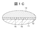
- FIG. 1C is a partially enlarged cross-sectional view showing the cross-sectional shape of each filtration flow path in the filtration filter.
- FIG. 2J It is process drawing of the manufacturing method of the filter for filtration concerning this Embodiment.
- FIGS. 1A to 1C are diagrams schematically illustrating a configuration of a filter for filtration manufactured by the method for manufacturing a filter for filtration according to the present embodiment
- FIG. 1A is a perspective view illustrating an appearance of the filter for filtration
- 1B is a partial cross-sectional view taken along line BB in FIG. 1A
- FIG. 1C is a partial enlarged cross-sectional view showing the cross-sectional shape of each filtration flow path in the filtration filter.
- a filter 10 for filtration includes, for example, a substrate 11 made of silicon, a flow path forming film 12 (first film) made of a thermal oxide film formed on the substrate 11, and the flow A channel sealing film 13 (second film) made of a thermal oxide film formed on the path forming film 12.
- the substrate 11 and the flow path forming film 12 are formed with inflow holes 14 (substrate penetrating portions) penetrating the substrate 11 and the flow path forming film 12 in the thickness direction.
- An outflow hole 15 (second membrane penetration part) penetrating the membrane 13 in the thickness direction is formed, and the inflow hole 14 and the outflow hole 15 are connected by a plurality of filtration channels 16.
- Each filtration channel 16 is formed along the surface of the substrate 11 and has a rectangular cross section as shown in FIG. 1C.
- the width of each filtration channel 16 is about 400 nm and the height is about 400 nm.
- the cross-sectional shape of the filtration flow path 16 is described as a rectangle, but the cross-sectional shape may be any shape as long as the inflow hole 14 and the outflow hole 15 can be essentially connected.
- the cross-sectional shape of the filtration channel 16 may be a trapezoid, a rectangle having a curved hypotenuse, a trapezoid, or the like.
- the fluid to be purified flows into the inflow holes 14, passes through the respective filtration channels 16, and flows out from the outflow holes 15.
- impurities larger than the cross section of each filtration channel 16 are removed from the fluid to be purified.
- a polymer compound smaller than the cross section of each filtration flow path 16 in the fluid to be purified can be purified.
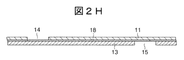
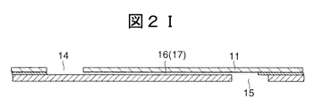
- FIGS. 2A to 2J are process diagrams of a method for manufacturing a filter for filtration according to the present embodiment.
- the method of forming the flow path forming film 12 is not limited to thermal CVD, and CVD using plasma, PVD (Physical Vapor Deposition), ALD (Atomic layer Deposition) may be used.
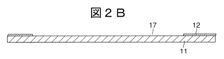
- a plurality of grooves 17 are formed in the flow path forming film 12 by a photolithography technique that is a semiconductor manufacturing technique. Specifically, a mask (not shown) having a pattern having openings corresponding to the plurality of grooves 17 to be formed is formed on the flow path forming film 12, and the flow paths exposed to the mask openings by etching with plasma or chemicals. By removing the formation film 12, a plurality of grooves 17 are formed along the surface of the substrate 11 (FIG. 2B) (groove formation step).
- FIG. 2B is a cross-sectional view taken along the groove 17.
- each groove 17 is, for example, 400 nm, and the grooves 17 are arranged side by side in the depth direction in the drawing and are arranged in parallel to each other.
- etching by plasma can perform high-precision processing not only in dimensions but also in shape rather than chemical etching.
- fine processing can be performed, but a vacuum environment is required as a processing environment. Therefore, the equipment for preparing the processing environment becomes large. In view of this, if highly accurate processing is not required for the size and shape, etching with a chemical solution can often prepare equipment for adjusting the processing environment at a lower cost.
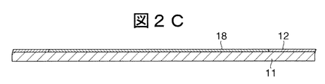
- the trench 17 is filled with a sacrificial film 18 made of a nitride film by CVD (sacrificial film filling step), and further, the sacrificial film 18 protruding from the trench 17 is polished by CMP (Chemical Mechanical Polishing) or the like. 12 and the surface of the sacrificial film 18 are flattened (FIG. 2C) (flattening step).
- the method for forming the sacrificial film 18 is not limited to CVD, and PVD or ALD may be used.
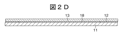
- the channel sealing film 13 is formed on the channel forming film 12 and the sacrificial film 18 by thermal CVD (FIG. 2) (second film forming step). Thereby, the sacrificial film 18 is sealed by the flow path sealing film 13.
- the film forming method of the flow path sealing film 13 is not limited to thermal CVD, and CVD using plasma, PVD, or ALD may be used.
- the substrate 11, the flow path forming film 12, the sacrificial film 18 and the flow path sealing film 13 are inverted with respect to the vertical direction, the substrate 11 is positioned at the uppermost position (FIG. 2F), and the bottom surface of the substrate 11 (the upper surface in the figure). ) Is polished by CMP or the like to thin the substrate 11 (FIG. 2G) (thinning step).
- vapor hydrofluoric acid is introduced into the inflow hole 14 or the outflow hole 15 to remove the sacrificial film 18 which is a nitride film (filtration channel forming step).
- the groove 17 from which the sacrificial film 18 has been removed forms the filtration channel 16 together with the channel sealing film 13 (FIG. 2I).
- the substrate 11, the flow path forming film 12, the sacrificial film 18 and the flow path sealing film 13 are inverted with respect to the vertical direction, the substrate 11 is positioned at the lowest position (FIG. 2J), and this process is completed.
- each groove 17 that forms each filtration flow path 16 in the flow path forming film 12 is formed by an etching technique used in semiconductor manufacturing.
- the width can be controlled accurately.
- highly accurate purification can be performed by using the filtration flow path 16 formed by the grooves 17.
- Etching is different from machining and the like, and a plurality of shapes can be formed and processed at a time. Therefore, by forming a plurality of grooves 17, the number of filtration channels 16 can be easily increased. The efficiency can be greatly improved.
- each filtration channel 16 is inversely proportional to the length of each filtration channel 16, but as described above, since the entire shape can be collectively formed and processed, the degree of freedom of the processing shape is high,
- the position of the inflow hole 14 and the outflow hole 15 and the length of the groove 17 can be freely set.
- the conductance of each filtration flow path 16 can be increased by shortening the length of each groove 17. Therefore, the efficiency of filtration can be improved by increasing the fluid to be purified flowing through each filtration flow path 16.
- the inflow hole 14 and the outflow hole 15 do not necessarily have to be provided in the vicinity of the end portion of the substrate 11. If the fluid to be purified before filtration and the fluid to be purified after filtration do not mix, the inflow holes 14 and the outflow holes 15 are located near the center of the substrate. You may provide close.
- the outflow hole 15 exposes one end of the sacrificial film 18, and the inflow hole 14 exposes the other end of the sacrificial film 18, thereby improving the efficiency of removing the sacrificial film 18. Therefore, the sacrificial film 18 can be prevented from remaining in the trench 17 and the time required for removing the sacrificial film 18 can be shortened.
- the substrate 11 is polished and thinned before the inflow hole 14 is formed in the substrate 11. The required time can be shortened.
- the inflow hole 14 is formed in the substrate 11 by etching. Therefore, when the inflow hole 14 is formed, the flow path sealing film 13 positioned below the substrate 11 contacts, for example, a mounting table on which the filtration filter 10 is mounted. Thereby, it is possible to prevent fine particles or the like scattered from the substrate 11 during etching from adhering to the flow path sealing film 13.
- the thickness of the flow path sealing film 13 can be freely adjusted.
- the thickness of the filter 10 for filtration can be made smaller than when the sacrificial film 18 is sealed with a glass substrate.
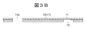
- FIGS. 3A to 3C are process diagrams of a modified example of the method for manufacturing the filter for filtration according to the present embodiment. Note that steps other than the steps shown in FIGS. 3A to 3C are the same as those in FIGS.
- the substrate 11, the flow path forming film 12, the sacrificial film 18 and the flow path sealing film 13 are inverted with respect to the vertical direction, and the bottom surface of the substrate 11 is polished to thin the substrate 11, that is, FIG.
- an inflow hole 14a penetrating the flow path forming film 12, the sacrificial film 18 and the flow path sealing film 13 is formed in the vicinity of the end portion of the sacrificial film 18 opposite to the outflow hole 15 by etching.
- the end (the other end) of the sacrificial film 18 is exposed on the side surface of the inflow hole 14a (FIG. 3A) (sacrificial film exposing step).
- vapor hydrofluoric acid is allowed to flow into the inflow hole 14a and the outflow hole 15 to remove the sacrificial film 18 that is a nitride film (filtration channel forming step).
- the groove 17 from which the sacrificial film 18 has been removed forms a filtration channel 16 (FIG. 3B).
- the substrate 11, the flow path forming film 12, the sacrificial film 18 and the flow path sealing film 13 are inverted with respect to the vertical direction, the substrate 11 is positioned at the lowest position (FIG. 3C), and this process is completed.
- the inflow hole 14a penetrates the substrate 11, the flow path forming film 12, and the flow path sealing film 13, the filtration is performed in a direction orthogonal to the main flow of the fluid to be purified.
- the opening area of each filtration flow path 16 on the side surface of the inflow hole 14a the flow ratio of the diversion that passes through the inflow hole 14a and the diversion that flows into the outflow hole 15 can be adjusted. The efficiency of the can be adjusted.
- the flow path forming film 12 and the flow path sealing film 13 are formed of a thermal oxide film and the sacrificial film 18 is formed of a nitride film.
- the flow path sealing film 13 may be formed of a nitride film, and the sacrificial film 18 may be formed of a thermal oxide film.
- the material in the manufacturing method of the filter for filtration mentioned above, there is no restriction on the material as long as the substrate 11 can be etched.
- a flexible material can be used as the substrate 11, so that the substrate 11 can be bent.
- a filter 10 for filtration can be manufactured.
- the use of the filter for filtration produced by the above-described method for producing a filter for filtration is not limited to the production of pharmaceuticals, for example, the field of food processing such as beer factories, and the field of water purification treatment such as household and commercial facilities. It can be expanded to wastewater treatment technology fields such as semiconductor factories and other fields that require high-precision filtration and treatment volume.
Landscapes
- Chemical & Material Sciences (AREA)
- Chemical Kinetics & Catalysis (AREA)
- Engineering & Computer Science (AREA)
- Manufacturing & Machinery (AREA)
- Water Supply & Treatment (AREA)
- Physics & Mathematics (AREA)
- Optics & Photonics (AREA)
- Nanotechnology (AREA)
- Dispersion Chemistry (AREA)
- Separation Using Semi-Permeable Membranes (AREA)
- Micromachines (AREA)
Abstract
Description
[図2A乃至図2J]本実施の形態に係る濾過用フィルタの製造方法の工程図である。
[図3A乃至図3C]本実施の形態に係る濾過用フィルタの製造方法の変形例の工程図である。
11 基板
12 流路形成膜
13 流路封止膜
14,14a 流入孔
15 流出孔
16 濾過用流路
17 溝
18 犠牲膜
Claims (7)
- 内部に濾過用流路を有する濾過用フィルタの製造方法であって、
基板上に第1の膜を形成する第1の膜形成ステップと、
前記第1の膜へ前記基板の表面に沿う溝をエッチングで形成する溝形成ステップと、
前記溝を犠牲膜で充填する犠牲膜充填ステップと、
前記犠牲膜を研磨して前記第1の膜の表面及び前記犠牲膜の表面を平坦化する平坦化ステップと、
前記第1の膜及び前記犠牲膜の上に第2の膜を形成する第2の膜形成ステップと、
前記基板の一部にエッチングで基板貫通部を形成し、前記第2の膜の一部にエッチングで第2の膜貫通部を形成し、前記基板貫通部及び前記第2の膜貫通部のそれぞれに前記犠牲膜の一部を露出させる犠牲膜露出ステップと、
前記基板貫通部及び前記第2の膜貫通部を介して前記犠牲膜を除去し、前記濾過用流路を前記溝で形成する濾過用流路形成ステップとを有することを特徴とする濾過用フィルタの製造方法。 - 前記第2の膜貫通部は前記犠牲膜の一端を露出させ、前記基板貫通部は前記犠牲膜の他端を露出させることを特徴とする請求項1記載の濾過用フィルタの製造方法。
- 前記基板貫通部に連通し、且つ前記第1の膜及び前記第2の膜を貫通する貫通孔を形成することを特徴とする請求項1又は2記載の濾過用フィルタの製造方法。
- 前記基板貫通部を形成する前に、前記基板を研磨して薄くする薄板化ステップを有することを特徴とする請求項1乃至3のいずれか1項に記載の濾過用フィルタの製造方法。
- 前記濾過用流路形成ステップでは、蒸気弗酸で前記犠牲膜を除去することを特徴とする請求項1乃至4のいずれか1項に記載の濾過用フィルタの製造方法。
- 前記第1の膜、前記第2の膜及び前記犠牲膜は、CVD、PVD及びALDのいずかで形成されることを特徴とする請求項1乃至5のいずれか1項に記載の濾過用フィルタの製造方法。
- 前記溝は複数形成されることを特徴とする請求項1乃至6のいずれか1項に記載の濾過用フィルタの製造方法。
Priority Applications (2)
| Application Number | Priority Date | Filing Date | Title |
|---|---|---|---|
| US14/427,650 US20150246317A1 (en) | 2012-09-19 | 2013-09-11 | Method for producing filtration filter |
| KR1020157006087A KR20150054816A (ko) | 2012-09-19 | 2013-09-11 | 여과용 필터의 제조 방법 |
Applications Claiming Priority (2)
| Application Number | Priority Date | Filing Date | Title |
|---|---|---|---|
| JP2012205482A JP2014057934A (ja) | 2012-09-19 | 2012-09-19 | 濾過用フィルタの製造方法 |
| JP2012-205482 | 2012-09-19 |
Publications (1)
| Publication Number | Publication Date |
|---|---|
| WO2014046151A1 true WO2014046151A1 (ja) | 2014-03-27 |
Family
ID=50341458
Family Applications (1)
| Application Number | Title | Priority Date | Filing Date |
|---|---|---|---|
| PCT/JP2013/075213 Ceased WO2014046151A1 (ja) | 2012-09-19 | 2013-09-11 | 濾過用フィルタの製造方法 |
Country Status (4)
| Country | Link |
|---|---|
| US (1) | US20150246317A1 (ja) |
| JP (1) | JP2014057934A (ja) |
| KR (1) | KR20150054816A (ja) |
| WO (1) | WO2014046151A1 (ja) |
Families Citing this family (1)
| Publication number | Priority date | Publication date | Assignee | Title |
|---|---|---|---|---|
| JP7008921B2 (ja) * | 2019-02-21 | 2022-02-10 | 株式会社オプトニクス精密 | フィルタ |
Citations (8)
| Publication number | Priority date | Publication date | Assignee | Title |
|---|---|---|---|---|
| JPS6164303A (ja) * | 1984-09-05 | 1986-04-02 | Hitachi Ltd | フイルタおよびその製造方法 |
| JPH09511439A (ja) * | 1994-03-07 | 1997-11-18 | ザ リージェンツ オブ ザ ユニバーシティ オブ カリフォルニア | 微小組み立てされた粒子フィルタ |
| JP2003305345A (ja) * | 2002-04-11 | 2003-10-28 | Toyo Kohan Co Ltd | 分離膜積層体および分離膜積層体を用いた部品 |
| JP2004209632A (ja) * | 2002-12-30 | 2004-07-29 | Internatl Business Mach Corp <Ibm> | 無機多孔メンブレンおよびその作成方法 |
| JP2005528975A (ja) * | 2002-01-07 | 2005-09-29 | サントゥル ナショナル ドゥ ラ ルシェルシュ シャーンティフィク(セ エン エール エス) | 貫通孔を有するシートの製造方法とミクロン及びサブミクロンフィルターの製造におけるその使用 |
| JP2006507105A (ja) * | 2002-02-13 | 2006-03-02 | ホスピラ・インコーポレイテツド | マイクロ流体抗菌フィルタ |
| WO2012063953A1 (ja) * | 2010-11-11 | 2012-05-18 | 東京エレクトロン株式会社 | 濾過用フィルタの製造方法 |
| WO2013146627A1 (ja) * | 2012-03-29 | 2013-10-03 | 東京エレクトロン株式会社 | 濾過用フィルタの製造方法 |
Family Cites Families (3)
| Publication number | Priority date | Publication date | Assignee | Title |
|---|---|---|---|---|
| US6153358A (en) * | 1996-12-23 | 2000-11-28 | Micorn Technology, Inc. | Polyimide as a mask in vapor hydrogen fluoride etching and method of producing a micropoint |
| US7384550B2 (en) * | 2004-02-24 | 2008-06-10 | Becton, Dickinson And Company | Glaucoma implant having MEMS filter module |
| JP5904958B2 (ja) * | 2013-03-07 | 2016-04-20 | 株式会社東芝 | 半導体マイクロ分析チップ及びその製造方法 |
-
2012
- 2012-09-19 JP JP2012205482A patent/JP2014057934A/ja not_active Withdrawn
-
2013
- 2013-09-11 WO PCT/JP2013/075213 patent/WO2014046151A1/ja not_active Ceased
- 2013-09-11 KR KR1020157006087A patent/KR20150054816A/ko not_active Withdrawn
- 2013-09-11 US US14/427,650 patent/US20150246317A1/en not_active Abandoned
Patent Citations (8)
| Publication number | Priority date | Publication date | Assignee | Title |
|---|---|---|---|---|
| JPS6164303A (ja) * | 1984-09-05 | 1986-04-02 | Hitachi Ltd | フイルタおよびその製造方法 |
| JPH09511439A (ja) * | 1994-03-07 | 1997-11-18 | ザ リージェンツ オブ ザ ユニバーシティ オブ カリフォルニア | 微小組み立てされた粒子フィルタ |
| JP2005528975A (ja) * | 2002-01-07 | 2005-09-29 | サントゥル ナショナル ドゥ ラ ルシェルシュ シャーンティフィク(セ エン エール エス) | 貫通孔を有するシートの製造方法とミクロン及びサブミクロンフィルターの製造におけるその使用 |
| JP2006507105A (ja) * | 2002-02-13 | 2006-03-02 | ホスピラ・インコーポレイテツド | マイクロ流体抗菌フィルタ |
| JP2003305345A (ja) * | 2002-04-11 | 2003-10-28 | Toyo Kohan Co Ltd | 分離膜積層体および分離膜積層体を用いた部品 |
| JP2004209632A (ja) * | 2002-12-30 | 2004-07-29 | Internatl Business Mach Corp <Ibm> | 無機多孔メンブレンおよびその作成方法 |
| WO2012063953A1 (ja) * | 2010-11-11 | 2012-05-18 | 東京エレクトロン株式会社 | 濾過用フィルタの製造方法 |
| WO2013146627A1 (ja) * | 2012-03-29 | 2013-10-03 | 東京エレクトロン株式会社 | 濾過用フィルタの製造方法 |
Also Published As
| Publication number | Publication date |
|---|---|
| US20150246317A1 (en) | 2015-09-03 |
| KR20150054816A (ko) | 2015-05-20 |
| JP2014057934A (ja) | 2014-04-03 |
Similar Documents
| Publication | Publication Date | Title |
|---|---|---|
| US11413383B2 (en) | Low resistance microfabricated filter | |
| JP2003175499A (ja) | マイクロ流体デバイス | |
| US9564386B2 (en) | Semiconductor package with structures for cooling fluid retention | |
| WO2003103836A1 (en) | Methods and devices for microfluidic extraction | |
| US20250153165A1 (en) | Silicon chip having multi-zone through silicon vias and method of manufacturing the same | |
| CN111001451A (zh) | 一种微流控芯片及基于微流控芯片的全血分离方法 | |
| US7537327B2 (en) | Internal die filters with multiple passageways which are fluidically in parallel | |
| WO2014046151A1 (ja) | 濾過用フィルタの製造方法 | |
| CN107285268B (zh) | 微流道散热芯片及其制备方法 | |
| US8580691B2 (en) | Method of forming non-planar membranes using CMP | |
| US10589204B2 (en) | Three dimensional nanometer filters and methods of use | |
| CN107481922A (zh) | 一种多孔悬膜及其制备方法 | |
| US7922924B2 (en) | Methods for making internal die filters with multiple passageways which are fluidically in parallel | |
| WO2012050420A1 (en) | Multilayer microfluidic filter and the method of fabricating thereof | |
| JP2013202559A (ja) | 濾過用フィルタの製造方法 | |
| US6579408B1 (en) | Apparatus and method for etching wafer backside | |
| CN105682769A (zh) | 岛蚀刻的过滤通道 |
Legal Events
| Date | Code | Title | Description |
|---|---|---|---|
| 121 | Ep: the epo has been informed by wipo that ep was designated in this application |
Ref document number: 13838861 Country of ref document: EP Kind code of ref document: A1 |
|
| ENP | Entry into the national phase |
Ref document number: 20157006087 Country of ref document: KR Kind code of ref document: A |
|
| WWE | Wipo information: entry into national phase |
Ref document number: 14427650 Country of ref document: US |
|
| NENP | Non-entry into the national phase |
Ref country code: DE |
|
| 122 | Ep: pct application non-entry in european phase |
Ref document number: 13838861 Country of ref document: EP Kind code of ref document: A1 |