WO2014045774A1 - 生体センサ、及び、生体センサの製造方法 - Google Patents
生体センサ、及び、生体センサの製造方法 Download PDFInfo
- Publication number
- WO2014045774A1 WO2014045774A1 PCT/JP2013/072057 JP2013072057W WO2014045774A1 WO 2014045774 A1 WO2014045774 A1 WO 2014045774A1 JP 2013072057 W JP2013072057 W JP 2013072057W WO 2014045774 A1 WO2014045774 A1 WO 2014045774A1
- Authority
- WO
- WIPO (PCT)
- Prior art keywords
- light
- emitting element
- receiving element
- light emitting
- sealing portion
- Prior art date
- Legal status (The legal status is an assumption and is not a legal conclusion. Google has not performed a legal analysis and makes no representation as to the accuracy of the status listed.)
- Ceased
Links
Images



Classifications
-
- A—HUMAN NECESSITIES
- A61—MEDICAL OR VETERINARY SCIENCE; HYGIENE
- A61B—DIAGNOSIS; SURGERY; IDENTIFICATION
- A61B5/00—Measuring for diagnostic purposes; Identification of persons
- A61B5/145—Measuring characteristics of blood in vivo, e.g. gas concentration or pH-value ; Measuring characteristics of body fluids or tissues, e.g. interstitial fluid or cerebral tissue
- A61B5/1455—Measuring characteristics of blood in vivo, e.g. gas concentration or pH-value ; Measuring characteristics of body fluids or tissues, e.g. interstitial fluid or cerebral tissue using optical sensors, e.g. spectral photometrical oximeters
- A61B5/14551—Measuring characteristics of blood in vivo, e.g. gas concentration or pH-value ; Measuring characteristics of body fluids or tissues, e.g. interstitial fluid or cerebral tissue using optical sensors, e.g. spectral photometrical oximeters for measuring blood gases
-
- A—HUMAN NECESSITIES
- A61—MEDICAL OR VETERINARY SCIENCE; HYGIENE
- A61B—DIAGNOSIS; SURGERY; IDENTIFICATION
- A61B5/00—Measuring for diagnostic purposes; Identification of persons
- A61B5/02—Detecting, measuring or recording for evaluating the cardiovascular system, e.g. pulse, heart rate, blood pressure or blood flow
- A61B5/024—Measuring pulse rate or heart rate
- A61B5/02416—Measuring pulse rate or heart rate using photoplethysmograph signals, e.g. generated by infrared radiation
- A61B5/02427—Details of sensor
- A61B5/02433—Details of sensor for infrared radiation
-
- A—HUMAN NECESSITIES
- A61—MEDICAL OR VETERINARY SCIENCE; HYGIENE
- A61B—DIAGNOSIS; SURGERY; IDENTIFICATION
- A61B5/00—Measuring for diagnostic purposes; Identification of persons
- A61B5/02—Detecting, measuring or recording for evaluating the cardiovascular system, e.g. pulse, heart rate, blood pressure or blood flow
- A61B5/024—Measuring pulse rate or heart rate
- A61B5/02444—Details of sensor
-
- A—HUMAN NECESSITIES
- A61—MEDICAL OR VETERINARY SCIENCE; HYGIENE
- A61B—DIAGNOSIS; SURGERY; IDENTIFICATION
- A61B5/00—Measuring for diagnostic purposes; Identification of persons
- A61B5/145—Measuring characteristics of blood in vivo, e.g. gas concentration or pH-value ; Measuring characteristics of body fluids or tissues, e.g. interstitial fluid or cerebral tissue
- A61B5/1455—Measuring characteristics of blood in vivo, e.g. gas concentration or pH-value ; Measuring characteristics of body fluids or tissues, e.g. interstitial fluid or cerebral tissue using optical sensors, e.g. spectral photometrical oximeters
- A61B5/14551—Measuring characteristics of blood in vivo, e.g. gas concentration or pH-value ; Measuring characteristics of body fluids or tissues, e.g. interstitial fluid or cerebral tissue using optical sensors, e.g. spectral photometrical oximeters for measuring blood gases
- A61B5/14552—Details of sensors specially adapted therefor
-
- H—ELECTRICITY
- H05—ELECTRIC TECHNIQUES NOT OTHERWISE PROVIDED FOR
- H05K—PRINTED CIRCUITS; CASINGS OR CONSTRUCTIONAL DETAILS OF ELECTRIC APPARATUS; MANUFACTURE OF ASSEMBLAGES OF ELECTRICAL COMPONENTS
- H05K3/00—Apparatus or processes for manufacturing printed circuits
- H05K3/22—Secondary treatment of printed circuits
- H05K3/28—Applying non-metallic protective coatings
- H05K3/284—Applying non-metallic protective coatings for encapsulating mounted components
-
- A—HUMAN NECESSITIES
- A61—MEDICAL OR VETERINARY SCIENCE; HYGIENE
- A61B—DIAGNOSIS; SURGERY; IDENTIFICATION
- A61B2562/00—Details of sensors; Constructional details of sensor housings or probes; Accessories for sensors
- A61B2562/12—Manufacturing methods specially adapted for producing sensors for in-vivo measurements
-
- A—HUMAN NECESSITIES
- A61—MEDICAL OR VETERINARY SCIENCE; HYGIENE
- A61B—DIAGNOSIS; SURGERY; IDENTIFICATION
- A61B2562/00—Details of sensors; Constructional details of sensor housings or probes; Accessories for sensors
- A61B2562/16—Details of sensor housings or probes; Details of structural supports for sensors
- A61B2562/166—Details of sensor housings or probes; Details of structural supports for sensors the sensor is mounted on a specially adapted printed circuit board
-
- A—HUMAN NECESSITIES
- A61—MEDICAL OR VETERINARY SCIENCE; HYGIENE
- A61B—DIAGNOSIS; SURGERY; IDENTIFICATION
- A61B2562/00—Details of sensors; Constructional details of sensor housings or probes; Accessories for sensors
- A61B2562/18—Shielding or protection of sensors from environmental influences, e.g. protection from mechanical damage
- A61B2562/185—Optical shielding, e.g. baffles
-
- H—ELECTRICITY
- H05—ELECTRIC TECHNIQUES NOT OTHERWISE PROVIDED FOR
- H05K—PRINTED CIRCUITS; CASINGS OR CONSTRUCTIONAL DETAILS OF ELECTRIC APPARATUS; MANUFACTURE OF ASSEMBLAGES OF ELECTRICAL COMPONENTS
- H05K1/00—Printed circuits
- H05K1/02—Details
- H05K1/0274—Optical details, e.g. printed circuits comprising integral optical means
-
- H—ELECTRICITY
- H05—ELECTRIC TECHNIQUES NOT OTHERWISE PROVIDED FOR
- H05K—PRINTED CIRCUITS; CASINGS OR CONSTRUCTIONAL DETAILS OF ELECTRIC APPARATUS; MANUFACTURE OF ASSEMBLAGES OF ELECTRICAL COMPONENTS
- H05K2201/00—Indexing scheme relating to printed circuits covered by H05K1/00
- H05K2201/09—Shape and layout
- H05K2201/09009—Substrate related
- H05K2201/09036—Recesses or grooves in insulating substrate
-
- H—ELECTRICITY
- H05—ELECTRIC TECHNIQUES NOT OTHERWISE PROVIDED FOR
- H05K—PRINTED CIRCUITS; CASINGS OR CONSTRUCTIONAL DETAILS OF ELECTRIC APPARATUS; MANUFACTURE OF ASSEMBLAGES OF ELECTRICAL COMPONENTS
- H05K3/00—Apparatus or processes for manufacturing printed circuits
- H05K3/30—Assembling printed circuits with electric components, e.g. with resistors
- H05K3/303—Assembling printed circuits with electric components, e.g. with resistors with surface mounted components
-
- Y—GENERAL TAGGING OF NEW TECHNOLOGICAL DEVELOPMENTS; GENERAL TAGGING OF CROSS-SECTIONAL TECHNOLOGIES SPANNING OVER SEVERAL SECTIONS OF THE IPC; TECHNICAL SUBJECTS COVERED BY FORMER USPC CROSS-REFERENCE ART COLLECTIONS [XRACs] AND DIGESTS
- Y10—TECHNICAL SUBJECTS COVERED BY FORMER USPC
- Y10T—TECHNICAL SUBJECTS COVERED BY FORMER US CLASSIFICATION
- Y10T29/00—Metal working
- Y10T29/49—Method of mechanical manufacture
- Y10T29/49002—Electrical device making
- Y10T29/49117—Conductor or circuit manufacturing
- Y10T29/49124—On flat or curved insulated base, e.g., printed circuit, etc.
- Y10T29/4913—Assembling to base an electrical component, e.g., capacitor, etc.
- Y10T29/49146—Assembling to base an electrical component, e.g., capacitor, etc. with encapsulating, e.g., potting, etc.
Definitions
- the present invention relates to a biological sensor that acquires a biological signal and a method of manufacturing the biological sensor.
- Patent Document 1 discloses a biological information measurement sensor having functions of both a biological electrode and an oximeter probe.
- This biological information measuring sensor includes an electrode element mounted on a polymer film, an LED as a light emitting element and a PD as a light receiving element, which are bonded and fixed on the electrode element via a predetermined interval, and each element.
- AMPS as a conductive transparent gel for coating.
- Patent Document 2 discloses a photoelectric pulse sensor composed of a light emitting element and a light receiving element.
- This photoelectric pulse sensor includes a substrate on which a light emitting element and a light receiving element are attached, and a base made of a light-transmitting material bonded to the substrate.
- a light-shielding plate made of a non-translucent material is inserted between the light-emitting part (light-emitting element) and the light-receiving part (light-receiving element) of the base made of a light-transmitting material.
- Patent Document 3 discloses an optical sensor that detects a pulsation of a blood flow rate as a change in light reflectance in a blood vessel and performs heartbeat detection based on the change.
- a light emitting element is arranged in the center as viewed from the light transmission surface of the casing
- a light shielding wall (partition wall) is formed in a shape surrounding the light emitting element
- a plurality of light receiving elements are arranged outside the light shielding wall.
- the outer wall surrounding the outside of the plurality of light receiving elements and the light shielding wall are connected by an intermediate wall.
- each space partitioned by the light shielding wall and the intermediate wall of the casing is filled with a light transmissive resin.
- the light emitting element (LED) and the light receiving element (PD) are covered with the conductive transparent gel (AMPS), and the LED and PD are transparent AMPS. It touches the skin of the living body through. Therefore, at the time of measurement, a part of light (detection light) emitted from the LED may reach the PD directly through the transparent AMPS.
- the light (stray light) that is emitted from the LED in this way and reaches the PD without being transmitted through the living body or reflected by the living body the intensity of the light is transmitted by the light that has passed through the living body or the living body. Larger than the intensity of the reflected light. Therefore, light that is originally desired to be detected, that is, light that has passed through the living body or light that has been reflected by the living body may be buried in stray light (noise), and the S / N ratio may be reduced.
- a light shielding wall is formed so as to surround the light emitting element disposed in the central portion of the casing, and a plurality of light receiving elements are disposed outside the light shielding wall. Moreover, the outer wall surrounding the outside of the plurality of light receiving elements and the light shielding wall are connected by an intermediate wall. Therefore, according to this optical sensor, it is possible to block stray light that reaches the light receiving element without being transmitted through the living body or reflected by the living body.
- this optical sensor requires a space for providing the above-described light-shielding wall (partition wall), outer wall, and intermediate wall on the substrate, so that the size of the sensor increases.
- the translucent resin used in the above-described biosensor has a large linear expansion coefficient.
- the linear expansion coefficient of the translucent resin is about 5 times larger. Therefore, if the translucent resin having a large thermal expansion coefficient has a large area in contact with the substrate on which the light emitting element and the light receiving element are mounted, the reliability of the sensor is lowered. More specifically, due to the difference in the linear expansion coefficient between the translucent resin and the substrate, for example, the substrate may be warped or the translucent resin may be peeled off from the substrate. There is also a risk that solder flash may occur during reflow in the soldered portion of the mounted electronic component.
- the present invention has been made to solve the above-described problems, and can reduce stray light received without passing through a living body without increasing the size and improving reliability.
- An object of the present invention is to provide a possible biosensor and a method of manufacturing the biosensor.
- the biosensor according to the present invention includes a wiring board, a light-emitting element and a light-receiving element mounted on the main surface of the wiring board at a predetermined interval, and a translucency formed only above the mounting area of the light-emitting element.
- a light-emitting element sealing portion having a light-transmitting property, a light-transmitting light-receiving element sealing portion formed only above the mounting region of the light-receiving element, and a light-emitting element sealing portion and a light-receiving portion formed on the main surface of the wiring board.
- the light-emitting element sealing part and the light-shielding part provided between the light-emitting element sealing part and the light-receiving element sealing part are provided.
- the light shielding part is provided around and between the light emitting element sealing part and the light receiving element sealing part. Therefore, stray light that is incident on the light receiving element without passing through the living body is blocked by the light shielding portion.
- the light emitting element sealing portion having translucency is formed only in the upper part of the mounting area of the light emitting element, and the light receiving element having translucency in only the upper part of the mounting area of the light receiving element. An element sealing portion is formed.
- the contact area between the translucent resin and the wiring board having different linear expansion coefficients can be reduced, so that the reliability of the biosensor can be improved.
- stray light received without passing through the living body can be reduced without increasing the size, and reliability can be improved.
- the light shielding portion, the light emitting element sealing portion, and the light receiving element sealing portion that form the top surface of the biosensor are formed flush with each other.
- the surface (top surface) of the biosensor that is touched by the subject's finger or the like is flattened, thereby preventing the subject from feeling uncomfortable when acquiring biometric information such as a photoelectric pulse wave signal. Is possible.
- the light emitting element sealing portion and the light receiving element sealing portion protrude in a curved shape from the top surface of the light shielding portion.
- the detection light emitted from the light emitting element and the detection light incident on the light receiving element can be collected, and the S / N ratio can be improved.
- a groove is formed around the light emitting element and the light receiving element on the main surface of the wiring board.
- the liquid translucent resin before solidifying spreads beyond the groove formed in the periphery. Can be prevented. Therefore, it is possible to form a light emitting element sealing portion and a light receiving element sealing portion having translucency only in the upper part of the mounting region of the light emitting element and the light receiving element.
- the inside of the groove is a mounting region for the light emitting element and the light receiving element.
- each of the light emitting element and the light receiving element is mounted on the wiring board via the sub board.
- the liquid translucent resin before solidification is prevented from spreading beyond the sub-substrate. Can do. Therefore, it is possible to form a light emitting element sealing portion and a light receiving element sealing portion having translucency only in the upper part of the mounting region of the light emitting element and the light receiving element.
- the mounting surface of the sub-board serves as a mounting area for the light emitting element and the light receiving element.
- each of the light emitting element and the light receiving element is preferably a surface mount type chip component. If it does in this way, it will become possible to achieve size reduction of a living body sensor.
- each of the light emitting element and the light receiving element is preferably a bare chip component. In this way, the mounting area of the light emitting element and the light receiving element can be further reduced, and the biosensor can be further miniaturized.
- each of the light emitting element sealing portion and the light receiving element sealing portion is preferably formed of a resin having translucency with respect to the wavelength of detection light emitted from the light emitting element.
- the wiring board is formed in a rectangular shape, and the light emitting element and the light receiving element are mounted at diagonal corners of the wiring board.
- the biosensor (wiring board) can be further downsized.
- the biosensor manufacturing method includes a substrate forming step of forming a wiring board, a mounting step of mounting a light emitting element and a light receiving element on the main surface of the wiring board with a predetermined interval, and mounting of the light emitting element.
- a light emitting element sealing step for forming a light emitting element sealing portion having a light transmitting property only on the upper portion of the region; and a light receiving element seal for forming a light receiving element sealing portion having a light transmitting property only on the upper portion of the mounting region of the light receiving element.
- a light shielding part is formed on the main surface of the wiring board, around the light emitting element sealing part and the light receiving element sealing part, and between the light emitting element sealing part and the light receiving element sealing part. And a forming step.
- the light shielding portion is formed around and between each of the light emitting element sealing portion and the light receiving element sealing portion.
- a biosensor capable of preventing stray light can be manufactured without forming a light shielding wall or the like for blocking stray light on the wiring board, that is, without increasing the size.
- the light emitting element sealing portion having translucency is formed only on the upper part of the light emitting element mounting area, and the light transmitting element is formed only on the upper part of the light receiving element mounting area.
- a light receiving element sealing portion having the structure is formed.
- biosensor manufacturing method it is preferable to further include a deletion step of forming the top surface of the biosensor including the light shielding portion, the light emitting element sealing portion, and the light receiving element sealing portion flush with each other.
- the surface (top surface) of the biosensor touched by the subject's finger or the like can be flattened. Therefore, for example, it is possible to prevent the subject from feeling uncomfortable when acquiring biological information such as a photoelectric pulse wave signal.
- the light shielding part is formed such that the tops of the light emitting element sealing part and the light receiving element sealing part protrude in a curved shape from the top surface of the light shielding part. It is preferable to do.
- the light shielding part is formed so that the tops of the light emitting element sealing part and the light receiving element sealing part protrude in a curved shape from the top surface of the light shielding part. Therefore, the detection light emitted from the light emitting element and the detection light incident on the light receiving element can be collected, and a biosensor with a high S / N ratio can be manufactured.
- grooves are formed around each of the light emitting element and the light receiving element on the main surface of the wiring board in the substrate forming step.
- the light emitting element sealing portion and the light receiving element sealing portion in the light emitting element sealing step and the light receiving element sealing step, the light transmitting property is exceeded beyond the grooves formed in the periphery. It is possible to prevent the resin from spreading. Therefore, it is possible to form a light emitting element sealing portion and a light receiving element sealing portion having translucency only in the upper part of the mounting region of the light emitting element and the light receiving element.
- each of the light emitting element and the light receiving element is mounted on the wiring board via the sub-board.
- the present invention it is possible to reduce stray light received without passing through a living body without causing an increase in size, and it is possible to improve reliability.
- FIG. 1 is a longitudinal sectional view of the biosensor 100.
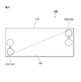
- FIG. 2 is a plan view showing the arrangement of the light emitting element 121 and the light receiving element 122 constituting the biological sensor 100 on the wiring board 110.
- the biological sensor 100 is a sensor that detects (measures) biological information such as a pulse and oxygen saturation by touching with a fingertip or the like.
- the biological sensor 100 optically measures a pulse, an oxygen saturation, etc. using the light absorption characteristics of blood hemoglobin.
- the biosensor 100 includes a wiring board 110, a light emitting element 121 and a light receiving element 122 mounted on the main surface 110 a of the wiring board 110, and a sealing portion 130 formed on the main surface 110 a of the wiring board 110.
- the sealing part 130 includes a light emitting element sealing part 131, a light receiving element sealing part 132, and a light shielding part 133.
- the wiring board 110 is, for example, a horizontally long and thin board formed of an insulating material (dielectric material) such as insulating resin or ceramics.
- a light emitting element 121, a light receiving element 122, and various electronic components are mounted on the main surface (mounting surface) 110 a of the wiring substrate 110.
- the light emitting element 121 and the light receiving element 122 are preferably mounted at corners located on the diagonal line of the wiring board 110.
- the light emitting element 121 and the light receiving element 122 are mounted with a predetermined interval, for example, an interval of about 4 to 20 mm.
- the light emitting element 121 emits light in the vicinity of infrared light having a high hemoglobin absorption coefficient, for example.
- the light receiving element 122 receives light emitted from the light emitting element 121 and transmitted through the living body or reflected by the living body (detection light), and outputs an electrical signal corresponding to the intensity of the received light.
- an LED As the light emitting element 121, an LED, a VCSEL (Vertical Cavity Surface Emitting LASER), a resonator type LED, or the like can be used.
- a photodiode (PD), a phototransistor, or the like is preferably used.
- a chip component (package product) of a surface mount type SMD: Surface Mount Device is preferably used.
- the sealing portion 130 is formed in a rectangular parallelepiped shape on the main surface 110 a of the wiring substrate 110, and the light emitting element sealing portion 131 that seals the light emitting element 121 and the light receiving element sealing portion 132 that seals the light receiving element 122. , And a light shielding portion 133.
- the light emitting element sealing portion 131 is formed of a translucent resin, for example, in a columnar shape (or a truncated cone shape), and seals the light emitting element 121.
- the light emitting element sealing portion 131 is formed only on the top of the component top surface of the light emitting element 121 (corresponding to the mounting region described in the claims).
- As the translucent resin forming the light emitting element sealing portion 131 for example, a transparent epoxy resin or the like is used.
- the light emitting element sealing portion 131 transmits light with respect to the wavelength (for example, infrared light) of the detection light emitted by the light emitting element 121 in order to absorb and cut light other than the detection light having a desired wavelength. It is preferable to form with resin which has property.
- the light receiving element sealing portion 132 is formed of, for example, a columnar shape (or a truncated cone shape) with a translucent resin, and seals the light receiving element 122.
- the light receiving element sealing portion 132 is formed only on the upper part of the light receiving element 122 (corresponding to the mounting region described in the claims).
- the translucent resin forming the light receiving element sealing portion 132 for example, a transparent epoxy resin or the like is used.
- the light receiving element sealing portion 132 transmits light with respect to the wavelength (for example, infrared light) of the detection light emitted by the light emitting element 121 in order to absorb and cut light other than the detection light having a desired wavelength. It is preferable that it is formed of a resin having properties.
- the light shielding portion 133 is formed on the main surface 110a of the wiring substrate 110, the area around the light emitting element sealing portion 131 and the light receiving element sealing portion 132, and the light emitting element sealing portion 131 and the light receiving element sealing portion 132. It is formed by filling a region having a light-shielding resin.
- the light shielding part 133 defines four side surfaces of the sealing part 130.
- an epoxy resin containing a light shielding powder such as carbon black is preferably used for the light shielding portion 133.
- each of the light emitting element sealing part 131, the light receiving element sealing part 132, and the light shielding part 133 defines a top surface 130a of the sealing part 130.
- the light emitting element sealing portion 131, the light receiving element sealing portion 132, and the light shielding portion 133 that form the top surface 130a of the biosensor 100 are formed so that the tops thereof are flush with each other. That is, the top surface 130a of the sealing part 130 was formed flat.
- FIG. 3 is a diagram illustrating a manufacturing process (manufacturing method) of the biosensor 100.
- the manufacturing process of the biosensor 100 mainly includes a substrate forming process, a mounting process, a light emitting element sealing process, a light receiving element sealing process, a light shielding part forming process, and a deletion process. .
- each step will be described.
- a horizontally elongated rectangular thin substrate board 110 made of, for example, insulating resin or ceramics, on which a wiring pattern is formed by etching or the like, is formed.
- the light emitting element 121, the light receiving element 122, and various electronic components are soldered and mounted on the main surface (mounting surface) 110 a of the wiring substrate 110 at predetermined positions.
- the light emitting element sealing step a translucent resin is applied (or molded or solid-bonded) to the component top surface of the light emitting element 121, for example.
- the light-emitting element sealing portion 131 having translucency is formed only on the top of the component top surface (mounting region) of the light-emitting element 121.
- the light emitting element sealing portion 131 is formed, for example, in a bell shape (or an inverted U shape).
- the light receiving element sealing step a light-transmitting resin is applied (or molded or solid-bonded), for example, to the component top surface of the light receiving element 122 in the same manner as the light emitting element sealing step described above.
- the light receiving element sealing portion 132 having translucency is formed only on the top of the component top surface (mounting region) of the light receiving element 122.
- the light receiving element sealing portion 132 is formed, for example, in a bell shape (or an inverted U shape). Further, the light emitting element sealing step and the light receiving element sealing step may be performed simultaneously.
- the light shielding part 133 is formed by filling an area between the stopper part 132 with an epoxy resin containing a light shielding powder such as carbon black.
- the light shielding element 131 and the light receiving element sealing part 132 are higher than the height of the light emitting element sealing part 131 and the light receiving element sealing part 132, that is, the light shielding element sealing part 131 and the light receiving element sealing part 132 are completely buried.
- the resin is filled.
- the top portions of the light emitting element sealing portion 131, the light receiving element sealing portion 132, and the light shielding portion 133 are formed by flushing, for example, by polishing or the like. Thereby, the tops of the light emitting element sealing portion 131 and the light receiving element sealing portion 132 are exposed to the top surface 130a of the biosensor 100 (sealing portion 130) and the top of the biosensor 100 (sealing portion 130).
- the surface 130a is formed flat.
- the upper portions of the bell-shaped (or inverted U-shaped) light emitting element sealing portion 131 and the light receiving element sealing portion 132 formed in the light emitting element sealing step and the light receiving element sealing step are cut off.
- the light emitting element sealing portion 131 and the light receiving element sealing portion 132 are formed in a columnar shape (or a truncated cone shape).
- the biosensor 100 is manufactured as described above.
- detection of a biological signal is performed by bringing the fingertip of the subject into contact with the surface (top surface 130a) of the biological sensor 100, for example.
- the light emitted from the light emitting element 121 enters the fingertip through the light emitting element sealing portion 131.
- Light incident on the fingertip and transmitted through the fingertip is incident on the opening of the light receiving element sealing portion 132.
- the light receiving element 122 receives light through the light receiving element sealing portion 132.
- transmitted the fingertip is acquired as a photoelectric pulse wave signal.
- the light shielding unit 133 is provided around and between each of the light emitting element sealing unit 131 and the light receiving element sealing unit 132. Therefore, the stray light that is incident on the light receiving element 122 without passing through the living body is blocked by the light shielding unit 133.
- the biological sensor 100 it is not necessary to provide a light shielding wall or the like for blocking stray light on the wiring board 110, and thus stray light is prevented without increasing the size of the wiring board 110 (biological sensor 100). (That is, the S / N ratio can be improved).
- the light-emitting element sealing portion 131 having translucency is formed only on the top of the component top surface (mounting region) of the light-emitting element 121, and the component top surface (mounting region) of the light-receiving element 122 is formed.
- a light receiving element sealing portion 132 having translucency is formed only on the upper part of the light receiving element. Therefore, the contact area between the translucent resin and the wiring board 110 having different linear expansion coefficients can be reduced, and thus the reliability of the biosensor 100 can be improved. As a result, according to the biosensor 100, it is possible to reduce stray light received without passing through the living body without causing an increase in size, and to improve reliability.
- the surface of the biosensor 100 (the top surface 130a of the sealing unit 130) that is touched by the subject's finger or the like is formed flat, and thus, for example, a photoelectric pulse wave signal or the like It is possible to prevent the subject from feeling uncomfortable when acquiring the biological signal.
- each of the light emitting element sealing portion 131 and the light receiving element sealing portion 132 has translucency with respect to the wavelength of the detection light emitted by the light emitting element 121, that is, desired.
- the resin selectively transmitting only the detection light having the wavelength to be transmitted, disturbance light (stray light) can be cut and only the detection light can be incident on the light receiving element 122. Therefore, the S / N ratio can be further improved.
- the wiring board 110 is formed in a rectangular shape, and the light emitting element 121 and the light receiving element 122 are mounted on the corners on the diagonal line of the wiring board 110.
- the width of the wiring board 110 can be shortened, and the biosensor 100 (wiring board 110) can be further downsized.
- FIG. 4 is a longitudinal sectional view of the biosensor 200 according to the first modification.
- Each of the light emitting element sealing portion 231 and the light receiving element sealing portion 232 according to this modification is formed in, for example, a bell shape (or an inverted U shape), and as described above, the top portion thereof is a light shielding portion. It is formed so as to protrude from the top surface of 233 into a curved surface (lens shape). Since other configurations are the same as or similar to those of the above-described biosensor 100, detailed description thereof is omitted here.
- the top portions of the light emitting element sealing portion 231 and the light receiving element sealing portion 232 protrude from the top surface 230e of the sealing portion 230 in the above-described forming process.
- the light shielding portion 233 is formed. That is, it is lower than the height of the light emitting element sealing portion 231 and the light receiving element sealing portion 232 and is filled with a light shielding resin. In this case, the above-described deletion process is not necessary.
- the detection light emitted from the light emitting element 121 and the detection light incident on the light receiving element 122 can be collected, and the S / N ratio can be further improved. It becomes possible.
- FIG. 5 is a longitudinal sectional view of the biosensor 300 according to the second modification. Since other configurations are the same as or similar to those of the above-described biosensor 100, detailed description thereof is omitted here.
- the mounting area of the light emitting element 321 and the light receiving element 322 can be further reduced, and the biosensor 300 can be further downsized.
- FIG. 6 is a longitudinal sectional view of the biosensor 400 according to the third modification.
- the biosensor 400 differs from the biosensor 100 described above in that it uses a wiring substrate 410 in which grooves 411 and 412 are formed around each of the light emitting element 121 and the light receiving element 122 instead of the above described wiring substrate 110. ing. Since other configurations are the same as or similar to those of the above-described biosensor 100, detailed description thereof is omitted here.
- the biosensor 400 when the light emitting element sealing portion 431 and the light receiving element sealing portion 432 are formed, for example, a liquid translucent resin before solidification is formed around the periphery. It is possible to prevent the grooves from extending beyond the grooves 411 and 412 formed. Therefore, the light-emitting element sealing portion 431 and the light-receiving element sealing portion 432 having translucency can be formed only in the upper portion of the mounting region of the light-emitting element 121 and the light-receiving element 122. This method is particularly effective when bare chip parts having no case are used as the light emitting element 121 and the light receiving element 122. In this case, the inside of the grooves 411 and 412 is a mounting region (a mounting region described in claims) of the light emitting element 431 and the light receiving element 432.
- FIG. 7 is a longitudinal sectional view of a biosensor 500 according to a fourth modification.
- the biosensor 500 is different from the biosensor 100 described above in that each of the light emitting element 121 and the light receiving element 122 is mounted on the wiring board 110 via the sub boards 511 and 512 (or spacers). Since other configurations are the same as or similar to those of the above-described biosensor 100, detailed description thereof is omitted here.
- the light emitting element 121 and the light receiving element 122 are mounted on the sub-boards 511 and 512 by soldering. Thereafter, the sub-boards 511 and 512 on which the light-emitting element 121 and the light-receiving element 122 are mounted are soldered to the wiring board 110.
- the liquid translucent resin before solidification is the sub-substrate 511.
- 512 can be prevented from spreading. Therefore, the light-emitting element sealing portion 531 and the light-receiving element sealing portion 532 having translucency can be formed only in the upper part of the mounting region of the light-emitting element 121 and the light-receiving element 122.
- This method is particularly effective when bare chip parts having no case are used as the light emitting element 121 and the light receiving element 122.
- the mounting surface of the sub-boards 511 and 512 is a mounting area for the light emitting element 121 and the light receiving element 122 (a mounting area described in claims).
- one light emitting element 121 is provided, but a plurality of light emitting elements may be provided. More specifically, in order to obtain an abundance ratio of oxyhemoglobin and reduced hemoglobin indicating blood oxygen saturation, two light emitting elements that emit light of different wavelengths may be provided. In this case, it is preferable that one light emitting element emits light in the vicinity of infrared light having a high extinction coefficient of oxyhemoglobin, and the other light emitting element emits light in the vicinity of red light having a high extinction coefficient of reduced hemoglobin. . In this case, a light emitting element sealing portion is formed above each light emitting element.
- the shapes of the light emitting element sealing portion 131 and the light receiving element sealing portion 132 are not limited to the above embodiment (columnar shape or truncated cone shape).
- the light emitting element sealing portion 131 and the light receiving element sealing portion 132 may be formed in, for example, a quadrangular prism shape or a square frustum shape in accordance with the shape (package shape) of the light emitting element / light receiving element.
- Biosensor 110 410 Wiring board 121, 321 Light emitting element 122, 322 Light receiving element 130, 230, 330, 430, 530 Sealing part 131, 231, 331, 431, 531 Light emitting element sealing Stop part 132,232,332,432,532 Light receiving element sealing part 133,233,333,433,533 Light shielding part 411,412 Groove 511,512 Sub-board
Landscapes
- Health & Medical Sciences (AREA)
- Life Sciences & Earth Sciences (AREA)
- Physics & Mathematics (AREA)
- Engineering & Computer Science (AREA)
- Medical Informatics (AREA)
- Animal Behavior & Ethology (AREA)
- Pathology (AREA)
- Veterinary Medicine (AREA)
- Biomedical Technology (AREA)
- Heart & Thoracic Surgery (AREA)
- Cardiology (AREA)
- Molecular Biology (AREA)
- Surgery (AREA)
- Biophysics (AREA)
- General Health & Medical Sciences (AREA)
- Public Health (AREA)
- Physiology (AREA)
- Spectroscopy & Molecular Physics (AREA)
- Optics & Photonics (AREA)
- Manufacturing & Machinery (AREA)
- Microelectronics & Electronic Packaging (AREA)
- Measurement Of The Respiration, Hearing Ability, Form, And Blood Characteristics Of Living Organisms (AREA)
- Measuring Pulse, Heart Rate, Blood Pressure Or Blood Flow (AREA)
Description
本発明は、生体信号を取得する生体センサ、及び、該生体センサの製造方法に関する。
近年、健康の管理や維持・増進に対する人々の関心が高まっている。そこでは、人々がより簡単に脈拍や心電などの生体情報を得られることが望まれている。ところで、従来から、血中のヘモグロビンが可視光~赤外光を吸収する特性を利用して、指等の生体を透過、又は生体に反射した光の強度変化を光電脈波信号として取得する脈拍計やパルスオキシメータが知られている(例えば特許文献1,2,3参照)。
ここで、特許文献1には、生体用電極とオキシメータプローブの両方の機能を持たせた生体情報測定用センサが開示されている。この生体情報測定用センサは、高分子フィルム上に取り付けられた電極素子と、該電極素子上に所定の間隔を介して接着固定された発光素子としてのLED及び受光素子としてのPDと、各素子を被覆する導電性透明ゲルとしてのAMPSとを備えている。このような構成を有することにより、センサを生体の皮膚の表面に接したときに、電極素子は導電性のあるAMPSを介して皮膚に接することにより、通常の電極素子としての機能を得ることができる。また、LED及びPDは透明なAMPSを介して皮膚に接するため、オキシメータプローブの機能を得ることができる。
特許文献2には、発光素子と受光素子より構成される光電式脈拍センサが開示されている。この光電式脈拍センサは、発光素子と受光素子とが取り付けられた基板と、該基板と接合される透光性の材質で構成された基台とを備えている。透光性の材質で構成された基台の発光部(発光素子)と受光部(受光素子)の中間には、非透光性材質の遮光板が挿入されている。
特許文献3には、血液流量の脈動を、血管での光反射率の変化として検知し、それに基づいて心拍検出を行う光学センサが開示されている。この光学センサでは、ケーシングの光透過面から見て中央部に発光素子が配置され、それを囲む形状で遮光壁(仕切り壁)が形成され、該遮光壁の外側に複数の受光素子が配置されている。該複数の受光素子の外側を囲む外壁と遮光壁とは、中間壁によって接続されている。また、ケーシングの遮光壁及び中間壁で仕切られた各々の空間には、光透過性の樹脂が充填されている
上述したように、特許文献1記載の生体情報測定用センサでは、発光素子(LED)と受光素子(PD)とが導電性透明ゲル(AMPS)で覆われており、LED及びPDは透明なAMPSを介して生体の皮膚に接する。そのため、測定時には、LEDから出射された光(検出光)の一部が透明なAMPSを通して直接PDに到達するおそれがある。通常、このようにLEDから出射され、生体を透過することなく、又は生体に反射されることなくPDに到達する光(迷光)は、その光の強度が、生体を透過した光、又は生体によって反射された光の強度と比較して大きい。そのため、本来検出したい光、すなわち生体を透過した光、又は生体によって反射された光が迷光(ノイズ)に埋もれてしまいS/N比が低下するおそれがある。
これに対して、特許文献2記載の光電式脈拍センサでは、発光部と受光部の中間に非透光性材質の遮光板が挿入されているため、発光素子から受光素子に直接到達する検出光(迷光)を遮断することができる。しかしながら、この光電式脈拍センサでは、透光性の材質で構成された基台の側面から外乱光(迷光)が入射するおそれがあり、特許文献1記載の生体情報測定用センサと同様にS/N比が低下するおそれがある。
特許文献3記載の光学センサでは、上述したように、ケーシングの中央部に配置された発光素子を囲むように遮光壁が形成され、該遮光壁の外側に複数の受光素子が配置されている。また、複数の受光素子の外側を囲む外壁と遮光壁とが、中間壁によって接続されている。そのため、この光学センサによれば、生体を透過することなく、又は生体に反射されることなく受光素子に到達する迷光を遮断することができる。しかしながら、この光学センサでは、基板上に上述した遮光壁(仕切り壁)、外壁、及び中間壁を設けるためのスペースが必要となりため、センサが大型化する。
また、一般的に、上述した生体センサに用いられる透光性を有する樹脂は線膨張係数が大きい。例えば、一般的なガラスエポキシ基板の線膨張係数と比較した場合に、透光性樹脂の線膨張係数は約5倍程度大きい。そのため、熱膨張係数の大きい透光性樹脂が発光素子及び受光素子の実装されている基板と接する面積が大きいと、センサの信頼性が低下する。より具体的には、透光性樹脂と基板との線膨張係数が異なることに起因して、例えば、基板の反りや、基板からの透光性樹脂の剥離等が生じるおそれがある。また、実装された電子部品のはんだ付け部においてリフロー時にはんだフラッシュが生じる等のおそれもある。
本発明は、上記問題点を解消する為になされたものであり、大型化を招くことなく生体を透過せずに受光される迷光を低減することができ、かつ、信頼性を向上することが可能な生体センサ、及び、該生体センサの製造方法を提供することを目的とする。
本発明に係る生体センサは、配線基板と、配線基板の主面に、所定の間隔を空けて実装された発光素子及び受光素子と、発光素子の実装領域の上部のみに形成された透光性を有する発光素子封止部と、受光素子の実装領域の上部のみに形成された透光性を有する受光素子封止部と、配線基板の主面上に形成され、発光素子封止部並びに受光素子封止部それぞれの周囲、及び、発光素子封止部と受光素子封止部との間に設けられた遮光部とを備えることを特徴とする。
本発明に係る生体センサによれば、発光素子封止部と受光素子封止部それぞれの周囲及び双方の間に遮光部が設けられている。よって、生体を透過せずに受光素子に入射される迷光は、該遮光部によって遮断される。ここで、配線基板上に迷光を遮断するための遮光壁等を設ける必要がないため、配線基板(生体センサ)の大型化を招くことなく、迷光を防止することができる。また、本発明に係る生体センサによれば、発光素子の実装領域の上部のみに透光性を有する発光素子封止部が形成され、受光素子の実装領域の上部のみに透光性を有する受光素子封止部が形成される。よって、線膨張係数が異なる透光性樹脂と配線基板との接触面積を縮小することができるため、生体センサの信頼性を向上することができる。以上の結果、大型化を招くことなく生体を透過せずに受光される迷光を低減することができ、かつ、信頼性を向上することが可能となる。
本発明に係る生体センサでは、生体センサの天面を形成する遮光部、発光素子封止部、及び受光素子封止部が、面一に形成されていることが好ましい。
このようにすれば、被験者の指等が触れる生体センサの表面(天面)が平坦になるため、例えば光電脈波信号等の生体情報を取得する際に被験者に違和感を与えることを防止することが可能となる。
本発明に係る生体センサでは、発光素子封止部、及び受光素子封止部が、遮光部の天面から、曲面状に突出していることが好ましい。
このようにすれば、発光素子から出射された検出光、及び受光素子に入射する検出光を集光することができ、S/N比を向上させることが可能となる。
本発明に係る生体センサでは、配線基板の主面には、発光素子及び受光素子の周囲に溝が形成されていることが好ましい。
このようにすれば、発光素子封止部、及び受光素子封止部を形成する際に、例えば、固化する前の液体状の透光性樹脂が、周囲に形成された溝を越えて広がることを防止することができる。よって、発光素子、受光素子の実装領域の上部のみに透光性を有する発光素子封止部、受光素子封止部を形成することが可能となる。なお、この場合には、上記溝の内側が発光素子、受光素子の実装領域となる。
本発明に係る生体センサでは、発光素子及び受光素子それぞれが、サブ基板を介して、配線基板に実装されていることが好ましい。
このようにすれば、発光素子封止部、及び受光素子封止部を形成する際に、例えば、固化する前の液体状の透光性樹脂が、サブ基板を越えて広がることを防止することができる。よって、発光素子、受光素子の実装領域の上部のみに透光性を有する発光素子封止部、受光素子封止部を形成することが可能となる。なお、この場合には、上記サブ基板の実装面が発光素子、受光素子の実装領域となる。
本発明に係る生体センサでは、発光素子及び受光素子それぞれが、表面実装タイプのチップ部品であることが好ましい。このようにすれば、生体センサの小型化を図ることが可能となる。
本発明に係る生体センサでは、発光素子及び受光素子それぞれが、ベアチップ部品であることが好ましい。このようにすれば、発光素子及び受光素子の実装面積をより減少させることができ、生体センサをより小型化することが可能となる。
本発明に係る生体センサでは、発光素子封止部及び受光素子封止部それぞれが、発光素子が発光する検出光の波長に対して透光性を有する樹脂により形成されていることが好ましい。
このようにすれば、外乱光(迷光)をカットして、所望する波長の検出光のみを受光素子に入射させることができるため、S/N比をより向上させることが可能となる。
本発明に係る生体センサでは、配線基板が矩形に形成されており、発光素子及び受光素子が、配線基板の対角線上の角部に実装されていることが好ましい。
このようにすれば、配線基板の幅を短縮することができるため、生体センサ(配線基板)をより小型化することができる。
本発明に係る生体センサの製造方法は、配線基板を形成する基板形成工程と、配線基板の主面に、所定の間隔を空けて発光素子及び受光素子を実装する実装工程と、発光素子の実装領域の上部のみに透光性を有する発光素子封止部を形成する発光素子封止工程と、受光素子の実装領域の上部のみに透光性を有する受光素子封止部を形成する受光素子封止工程と、配線基板の主面上に、かつ、発光素子封止部並びに受光素子封止部それぞれの周囲、及び、発光素子封止部と受光素子封止部との間に遮光部を形成する形成工程とを備えることを特徴とする。
本発明に係る生体センサの製造方法によれば、発光素子封止部と受光素子封止部それぞれの周囲及び双方の間に遮光部が形成される。このようにすれば、配線基板上に迷光を遮断するための遮光壁等を形成することなく、すなわち、大型化を招くことなく、迷光を防止可能な生体センサを製造することができる。また、本発明に係る生体センサの製造方法によれば、発光素子の実装領域の上部のみに透光性を有する発光素子封止部が形成され、受光素子の実装領域の上部のみに透光性を有する受光素子封止部が形成される。よって、線膨張係数が異なる透光性樹脂と配線基板との接触面積を縮小することができるため、信頼性の高い生体センサを製造することができる。以上の結果、大型化を招くことなく生体を透過せずに受光される迷光を低減することができ、かつ、信頼性の高い生体センサを製造することが可能となる。
本発明に係る生体センサの製造方法では、遮光部、発光素子封止部、及び受光素子封止部からなる生体センサの天面を面一に形成する削除工程をさらに備えることが好ましい。
このようにすれば、被験者の指等が触れる生体センサの表面(天面)を平坦にすることができる。そのため、例えば光電脈波信号等の生体情報を取得する際に被験者に違和感を与えることを防止することが可能となる。
本発明に係る生体センサの製造方法では、形成工程において、発光素子封止部、及び受光素子封止部それぞれの頂部が、遮光部の天面から、曲面状に突出するように遮光部を形成することが好ましい。
この場合、発光素子封止部、及び受光素子封止部それぞれの頂部が、遮光部の天面から、曲面状に突出するように遮光部が形成される。そのため、発光素子から出射された検出光、及び受光素子に入射する検出光を集光することができ、S/N比の高い生体センサを製造することが可能となる。
本発明に係る生体センサの製造方法では、基板形成工程において、配線基板の主面の発光素子及び受光素子それぞれの周囲に溝を形成することが好ましい。
このようにすれば、発光素子封止工程、及び受光素子封止工程において、発光素子封止部、及び受光素子封止部を形成する際に、周囲に形成された溝を越えて透光性樹脂が広がることを防止することができる。よって、発光素子、受光素子の実装領域の上部のみに透光性を有する発光素子封止部、受光素子封止部を形成することが可能となる。
本発明に係る生体センサの製造方法では、実装工程において、サブ基板を介して、発光素子及び受光素子それぞれを、配線基板に実装することが好ましい。
このようにすれば、発光素子封止工程、及び受光素子封止工程において、発光素子封止部、及び受光素子封止部を形成する際に、サブ基板を越えて透光性樹脂が広がることを防止することができる。よって、発光素子、受光素子の実装領域の上部のみに透光性を有する発光素子封止部、受光素子封止部を形成することが可能となる。
本発明によれば、大型化を招くことなく生体を透過せずに受光される迷光を低減することができ、かつ、信頼性を向上することが可能となる。
以下、図面を参照して本発明の好適な実施形態について詳細に説明する。なお、各図において、同一要素には同一符号を付して重複する説明を省略する。
まず、図1,図2を併せて用いて、実施形態に係る生体センサ100の構成について説明する。図1は、生体センサ100の縦断面図である。また、図2は、生体センサ100を構成する発光素子121と受光素子122の配線基板上110の配置を示す平面図である。
生体センサ100は、指先などで触れることにより、例えば、脈拍、酸素飽和度などの生体情報を検出(計測)するセンサである。生体センサ100は、血中ヘモグロビンの吸光特性を利用して、脈拍や酸素飽和度などを光学的に計測する。
そのため、生体センサ100は、配線基板110、配線基板110の主面110aに実装された発光素子121と受光素子122、及び、配線基板110の主面110a上に形成された封止部130を備えて構成されている。なお、封止部130は、発光素子封止部131、受光素子封止部132、及び、遮光部133を含んで構成されている。
配線基板110は、例えば、絶縁性の樹脂やセラミックスなどの絶縁体(誘電体)から形成された横長矩形で薄板形状の基板である。配線基板110の主面(実装面)110aには、発光素子121、受光素子122、及び各種電子部品が実装されている。ここで、図2に示されるように、発光素子121及び受光素子122は、配線基板110の対角線上に位置する角部に実装されることが好ましい。また、発光素子121と受光素子122とは、所定の間隔、例えば4~20mm程度の間隔を空けて実装される。
発光素子121は、例えば、ヘモグロビンの吸光係数が高い赤外光付近の光を出射する。一方、受光素子122は、発光素子121から出射され、生体を透過した光、又は生体によって反射された光(検出光)を受光し、受光した光の強度に応じた電気信号を出力する。
発光素子121としては、LED、VCSEL(Vertical Cavity Surface Emitting LASER)、又は共振器型LED等を用いることができる。受光素子122としては、フォトダイオード(PD)又はフォトトランジスタ等が好適に用いられる。なお、発光素子121及び受光素子122としては、表面実装タイプ(SMD:Surface Mount Device)のチップ部品(パッケージ品)が好適に用いられる。
封止部130は、配線基板110の主面110a上に直方体状に形成されており、発光素子121を封止する発光素子封止部131、受光素子122を封止する受光素子封止部132、及び遮光部133から構成されている。
発光素子封止部131は、透光性樹脂によって、例えば円柱状(又は円錐台状)に形成され、発光素子121を封止している。発光素子封止部131は、発光素子121の部品天面(請求の範囲に記載の実装領域に相当)の上部のみに形成されている。発光素子封止部131を形成する透光性樹脂としては、例えば、透明なエポキシ樹脂等が用いられる。ここで、発光素子封止部131は、所望する波長の検出光以外の光を吸収してカットするために、発光素子121が発光する検出光の波長(例えば赤外光)に対して透光性を有する樹脂により形成されることが好ましい。
また、受光素子封止部132は、透光性樹脂によって、例えば円柱状(又は円錐台状)に形成され、受光素子122を封止している。受光素子封止部132は、受光素子122の部品天面(請求の範囲に記載の実装領域に相当)の上部のみに形成されている。受光素子封止部132を形成する透光性樹脂としては、例えば、透明なエポキシ樹脂等が用いられる。ここで、受光素子封止部132は、所望する波長の検出光以外の光を吸収してカットするために、発光素子121が発光する検出光の波長(例えば赤外光)に対して透光性を有する樹脂により形成されていることが好ましい。
遮光部133は、配線基板110の主面110a上に、発光素子封止部131と受光素子封止部132それぞれの周囲の領域、及び、発光素子封止部131と受光素子封止部132との間の領域に遮光性を有する樹脂が充填されることによって形成される。この遮光部133は、封止部130の4方の側面を画している。なお、遮光部133には、カーボンブラック等の遮光性のある粉末を含有するエポキシ樹脂等が好適に用いられる。
発光素子封止部131、受光素子封止部132、及び遮光部133それぞれの上部の面は、封止部130の天面130aを画している。本実施形態では、生体センサ100の天面130aを形成する発光素子封止部131、受光素子封止部132、及び、遮光部133それぞれの頂部が面一になるように形成した。すなわち、封止部130の天面130aを平坦に形成した。
次に、図3を参照しつつ、本実施形態に係る生体センサ100の製造工程(製造方法)について説明する。ここで、図3は、生体センサ100の製造工程(製造方法)を示す図である。図3に示されるように、生体センサ100の製造工程は、主として、基板形成工程、実装工程、発光素子封止工程、受光素子封止工程、遮光部形成工程、及び、削除工程から成っている。以下、各工程について説明する。
(基板形成工程)
まず、基板形成工程では、エッチング等により配線パターンが形成された、例えば絶縁性の樹脂やセラミックスなどからなる、横長矩形で薄板形状の配線基板110が形成される。
まず、基板形成工程では、エッチング等により配線パターンが形成された、例えば絶縁性の樹脂やセラミックスなどからなる、横長矩形で薄板形状の配線基板110が形成される。
(実装工程)
次に、実装工程では、配線基板110の主面(実装面)110aに、発光素子121、受光素子122、及び各種電子部品が、所定の位置にはんだ付けされて実装される。
次に、実装工程では、配線基板110の主面(実装面)110aに、発光素子121、受光素子122、及び各種電子部品が、所定の位置にはんだ付けされて実装される。
(発光素子封止工程)
発光素子封止工程では、発光素子121の部品天面に、透光性樹脂が、例えば、塗布(又は、モールドや固形接着)される。これにより、発光素子121の部品天面(実装領域)の上部のみに、透光性を有する発光素子封止部131が形成される。なお、ここでは、発光素子封止部131は、例えば、釣鐘型(又は逆U字状)に形成される。
発光素子封止工程では、発光素子121の部品天面に、透光性樹脂が、例えば、塗布(又は、モールドや固形接着)される。これにより、発光素子121の部品天面(実装領域)の上部のみに、透光性を有する発光素子封止部131が形成される。なお、ここでは、発光素子封止部131は、例えば、釣鐘型(又は逆U字状)に形成される。
(受光素子封止工程)
また、受光素子封止工程では、上述した発光素子封止工程と同様にして、受光素子122の部品天面に、透光性樹脂が、例えば、塗布(又は、モールドや固形接着)される。これにより、受光素子122の部品天面(実装領域)の上部のみに、透光性を有する受光素子封止部132が形成される。なお、ここででは、受光素子封止部132は、例えば、釣鐘型(又は逆U字状)に形成される。また、発光素子封止工程と受光素子封止工程とは同時に行ってもよい。
また、受光素子封止工程では、上述した発光素子封止工程と同様にして、受光素子122の部品天面に、透光性樹脂が、例えば、塗布(又は、モールドや固形接着)される。これにより、受光素子122の部品天面(実装領域)の上部のみに、透光性を有する受光素子封止部132が形成される。なお、ここででは、受光素子封止部132は、例えば、釣鐘型(又は逆U字状)に形成される。また、発光素子封止工程と受光素子封止工程とは同時に行ってもよい。
(遮光部形成工程)
続いて、遮光部形成工程では、配線基板110の主面110a上に、発光素子封止部131と受光素子封止部132それぞれの周囲の領域、及び、発光素子封止部131と受光素子封止部132との間の領域に、カーボンブラック等の遮光性のある粉末を含有するエポキシ樹脂等が充填されることによって遮光部133が形成される。なお、ここでは、発光素子封止部131、及び受光素子封止部132の高さよりも高く、すなわち、発光素子封止部131、及び受光素子封止部132が完全に埋没するように、遮光性樹脂が充填される。
続いて、遮光部形成工程では、配線基板110の主面110a上に、発光素子封止部131と受光素子封止部132それぞれの周囲の領域、及び、発光素子封止部131と受光素子封止部132との間の領域に、カーボンブラック等の遮光性のある粉末を含有するエポキシ樹脂等が充填されることによって遮光部133が形成される。なお、ここでは、発光素子封止部131、及び受光素子封止部132の高さよりも高く、すなわち、発光素子封止部131、及び受光素子封止部132が完全に埋没するように、遮光性樹脂が充填される。
(削除工程)
そして、削除工程では、発光素子封止部131、受光素子封止部132、及び、遮光部133それぞれの頂部が、例えば、研磨等で削り出されることにより、面一に形成される。これにより、発光素子封止部131、受光素子封止部132の頂部が、生体センサ100(封止部130)の天面130aに露出されるとともに、生体センサ100(封止部130)の天面130aが平坦に形成される。なお、この工程では、発光素子封止工程、受光素子封止工程において形成された、釣鐘型(又は逆U字状)の発光素子封止部131、受光素子封止部132の上部が切除され、発光素子封止部131、受光素子封止部132が、円柱状(又は円錐台状)に形成される。以上のようにして、生体センサ100が製造される。
そして、削除工程では、発光素子封止部131、受光素子封止部132、及び、遮光部133それぞれの頂部が、例えば、研磨等で削り出されることにより、面一に形成される。これにより、発光素子封止部131、受光素子封止部132の頂部が、生体センサ100(封止部130)の天面130aに露出されるとともに、生体センサ100(封止部130)の天面130aが平坦に形成される。なお、この工程では、発光素子封止工程、受光素子封止工程において形成された、釣鐘型(又は逆U字状)の発光素子封止部131、受光素子封止部132の上部が切除され、発光素子封止部131、受光素子封止部132が、円柱状(又は円錐台状)に形成される。以上のようにして、生体センサ100が製造される。
本実施形態に係る生体センサ100によれば、生体信号の検出は、例えば被検者の指先を生体センサ100の表面(天面130a)に接触させることにより行われる。生体センサ100の表面に指先を接触させた場合、発光素子121から出射された光が、発光素子封止部131を通して指先に入射される。指先に入射され、該指先を透過した光は、受光素子封止部132の開口部に入射される。そして、受光素子封止部132を通して受光素子122によって受光される。これにより、指先を透過した検出光の強度変化が光電脈波信号として取得される。
以上、説明したように、本実施形態に係る生体センサ100によれば、発光素子封止部131と受光素子封止部132それぞれの周囲及び双方の間に遮光部133が設けられている。よって、生体を透過せずに受光素子122に入射される迷光は、該遮光部133によって遮断される。ここで、生体センサ100によれば、配線基板110上に迷光を遮断するための遮光壁等を設ける必要がないため、配線基板110(生体センサ100)の大型化を招くことなく、迷光を防止(すなわちS/N比を向上)することができる。また、生体センサ100によれば、発光素子121の部品天面(実装領域)の上部のみに透光性を有する発光素子封止部131が形成され、受光素子122の部品天面(実装領域)の上部のみに透光性を有する受光素子封止部132が形成される。よって、線膨張係数が異なる透光性樹脂と配線基板110との接触面積を縮小することができるため、生体センサ100の信頼性を向上することができる。以上の結果、生体センサ100によれば、大型化を招くことなく生体を透過せずに受光される迷光を低減することができ、かつ、信頼性を向上することが可能となる。
また、本実施形態に係る生体センサ100によれば、被験者の指等が触れる生体センサ100の表面(封止部130の天面130a)が平坦に形成されているため、例えば光電脈波信号等の生体信号を取得する際に被験者に違和感を与えることを防止することが可能となる。
本実施形態に係る生体センサ100によれば、発光素子封止部131及び受光素子封止部132それぞれが、発光素子121が発光する検出光の波長に対して透光性を有する、すなわち、所望する波長の検出光のみを選択的に透過する樹脂により形成されることにより、外乱光(迷光)をカットして、検出光のみを受光素子122に入射させることができる。よって、S/N比をより向上させることが可能となる。
また、本実施形態に係る生体センサ100によれば、配線基板110が矩形に形成されており、発光素子121及び受光素子122が、配線基板110の対角線上の角部に実装されているため、配線基板110の幅を短縮することができ、生体センサ100(配線基板110)をより小型化することができる。
(第1変形例)
上記実施形態では、生体センサ100の表面(封止部130の天面130a)を平坦に形成、すなわち、発光素子封止部131、受光素子封止部132、及び、遮光部133それぞれの頂部が面一になるように形成したが、図4に示されるように、発光素子封止部231、及び受光素子封止部232の頂部が、遮光部233の天面から、曲面状に突出するように形成してもよい。ここで、図4は、第1変形例に係る生体センサ200の縦断面図である。
上記実施形態では、生体センサ100の表面(封止部130の天面130a)を平坦に形成、すなわち、発光素子封止部131、受光素子封止部132、及び、遮光部133それぞれの頂部が面一になるように形成したが、図4に示されるように、発光素子封止部231、及び受光素子封止部232の頂部が、遮光部233の天面から、曲面状に突出するように形成してもよい。ここで、図4は、第1変形例に係る生体センサ200の縦断面図である。
本変形例に係る発光素子封止部231、及び受光素子封止部232それぞれは、例えば、釣鐘型(又は逆U字状)に形成されており、上述したように、その頂部が、遮光部233の天面から、曲面状(レンズ状)に突出するように形成されている。なお、その他の構成は、上述した生体センサ100と同一又は同様であるので、ここでは詳細な説明を省略する。
本変形例に係る生体センサ200を製造する際には、上述した形成工程において、発光素子封止部231、及び受光素子封止部232それぞれの頂部が、封止部230の天面230eから突出するように遮光部233が形成される。すなわち、発光素子封止部231、及び受光素子封止部232の高さよりも低く、遮光性樹脂が充填される。また、この場合、上述した削除工程は不要となる。
第1変形例に係る生体センサ200によれば、発光素子121から出射された検出光、及び受光素子122に入射する検出光を集光することができ、S/N比をより向上させることが可能となる。
(第2変形例)
上記実施形態では、発光素子121及び受光素子122として、表面実装タイプ(SMD)のチップ部品を用いたが、図5に示されるように、ベアチップ部品321,322を用いることも好ましい。ここで、図5は、第2変形例に係る生体センサ300の縦断面図である。なお、その他の構成は、上述した生体センサ100と同一又は同様であるので、ここでは詳細な説明を省略する。
上記実施形態では、発光素子121及び受光素子122として、表面実装タイプ(SMD)のチップ部品を用いたが、図5に示されるように、ベアチップ部品321,322を用いることも好ましい。ここで、図5は、第2変形例に係る生体センサ300の縦断面図である。なお、その他の構成は、上述した生体センサ100と同一又は同様であるので、ここでは詳細な説明を省略する。
本実施形態に係る生体センサ300によれば、発光素子321及び受光素子322の実装面積をより減少させることができ、生体センサ300をより小型化することが可能となる。
(第3変形例)
続いて、図6を参照して、第3変形例に係る生体センサ400の構成について説明する。ここで、図6は、第3変形例に係る生体センサ400の縦断面図である。生体センサ400は、上述した配線基板110に代えて、発光素子121及び受光素子122それぞれの周囲に溝411,412が形成された配線基板410を用いている点で、上述した生体センサ100と異なっている。なお、その他の構成は、上述した生体センサ100と同一又は同様であるので、ここでは詳細な説明を省略する。
続いて、図6を参照して、第3変形例に係る生体センサ400の構成について説明する。ここで、図6は、第3変形例に係る生体センサ400の縦断面図である。生体センサ400は、上述した配線基板110に代えて、発光素子121及び受光素子122それぞれの周囲に溝411,412が形成された配線基板410を用いている点で、上述した生体センサ100と異なっている。なお、その他の構成は、上述した生体センサ100と同一又は同様であるので、ここでは詳細な説明を省略する。
本変形例に係る生体センサ400を製造する際には、上述した基板形成工程において、例えば切削加工等により、配線基板410の主面410aの発光素子121及び受光素子122それぞれの周囲に溝411,412が形成される。
本実施形態に係る生体センサ400によれば、発光素子封止部431、及び受光素子封止部432を形成する際に、例えば、固化する前の液体状の透光性樹脂が、周囲に形成された溝411,412を越えて広がることを防止することができる。よって、発光素子121・受光素子122の実装領域の上部のみに透光性を有する発光素子封止部431、受光素子封止部432を形成することが可能となる。この方法は、特に、発光素子121、受光素子122として、ケースを有しないベアチップ部品を用いるときに有効である。また、この場合には、上記溝411,412の内側が発光素子431、受光素子432の実装領域(請求の範囲に記載の実装領域)となる。
(第4変形例)
続いて、図7を参照して、第4変形例に係る生体センサ500の構成について説明する。ここで、図7は、第4変形例に係る生体センサ500の縦断面図である。生体センサ500は、発光素子121及び受光素子122それぞれがサブ基板511,512(又はスペーサ)を介して、配線基板110に実装されている点で、上述した生体センサ100と異なっている。なお、その他の構成は、上述した生体センサ100と同一又は同様であるので、ここでは詳細な説明を省略する。
続いて、図7を参照して、第4変形例に係る生体センサ500の構成について説明する。ここで、図7は、第4変形例に係る生体センサ500の縦断面図である。生体センサ500は、発光素子121及び受光素子122それぞれがサブ基板511,512(又はスペーサ)を介して、配線基板110に実装されている点で、上述した生体センサ100と異なっている。なお、その他の構成は、上述した生体センサ100と同一又は同様であるので、ここでは詳細な説明を省略する。
本変形例に係る生体センサ400を製造する際には、上述した実装工程において、まず、サブ基板511,512に発光素子121、受光素子122がはんだ付けによって実装される。その後、発光素子121、受光素子122が実装されたサブ基板511,512が、配線基板110にはんだ付けされる。
本実施形態に係る生体センサ500によれば、発光素子封止部531、及び受光素子封止部532を形成する際に、例えば、固化する前の液体状の透光性樹脂が、サブ基板511,512を越えて広がることを防止することができる。よって、発光素子121、受光素子122の実装領域の上部のみに透光性を有する発光素子封止部531、受光素子封止部532を形成することが可能となる。この方法は、特に、発光素子121、受光素子122として、ケースを有しないベアチップ部品を用いるときに有効である。また、この場合には、上記サブ基板511,512の実装面が発光素子121、受光素子122の実装領域(請求の範囲に記載の実装領域)となる。
以上、本発明の実施の形態について説明したが、本発明は、上記実施形態に限定されるものではなく種々の変形が可能である。例えば、上記実施形態では、1つの発光素子121を有していたが、複数の発光素子を有していてもよい。より具体的には、血中酸素飽和度を示す酸化ヘモグロビンと還元ヘモグロビンとの存在比を得るために、異なる波長の光を出射する2つの発光素子を有していてもよい。この場合、一方の発光素子は、酸化ヘモグロビンの吸光係数が高い赤外光付近の光を出射し、他方の発光素子は、還元ヘモグロビンの吸光係数が高い赤色光付近の光を出射することが好ましい。また、この場合には、各発光素子の上部に発光素子封止部が形成される。
また、発光素子封止部131、受光素子封止部132の形状は、上記実施形態(円柱状又は円錐台状)には限られない。発光素子封止部131、受光素子封止部132は、発光素子・受光素子の形状(パッケージ形状)に合わせて、例えば、四角柱状や、四角錐台状に形成してもよい。
100,200,300,400,500 生体センサ
110,410 配線基板
121,321 発光素子
122,322 受光素子
130,230,330,430,530 封止部
131,231,331,431,531 発光素子封止部
132,232,332,432,532 受光素子封止部
133,233,333,433,533 遮光部
411,412 溝
511,512 サブ基板
110,410 配線基板
121,321 発光素子
122,322 受光素子
130,230,330,430,530 封止部
131,231,331,431,531 発光素子封止部
132,232,332,432,532 受光素子封止部
133,233,333,433,533 遮光部
411,412 溝
511,512 サブ基板
Claims (14)
- 配線基板と、
前記配線基板の主面に、所定の間隔を空けて実装された発光素子及び受光素子と、
前記発光素子の実装領域の上部のみに形成された透光性を有する発光素子封止部と、
前記受光素子の実装領域の上部のみに形成された透光性を有する受光素子封止部と、
前記配線基板の主面上に形成され、前記発光素子封止部並びに前記受光素子封止部それぞれの周囲、及び、前記発光素子封止部と前記受光素子封止部との間に設けられた遮光部と、を備えることを特徴とする生体センサ。 - 前記生体センサの天面を形成する前記遮光部、前記発光素子封止部、及び前記受光素子封止部は、面一に形成されていることを特徴とする請求項1に記載の生体センサ。
- 前記発光素子封止部、及び前記受光素子封止部は、前記遮光部の天面から、曲面状に突出していることを特徴とする請求項1に記載の生体センサ。
- 前記配線基板の主面には、前記発光素子及び前記受光素子の周囲に溝が形成されていることを特徴とする請求項1~3のいずれか1項に記載の生体センサ。
- 前記発光素子及び前記受光素子それぞれは、サブ基板を介して、前記配線基板に実装されていることを特徴とする請求項1~3のいずれか1項に記載の生体センサ。
- 前記発光素子及び前記受光素子それぞれは、表面実装タイプのチップ部品であることを特徴とする請求項1~5のいずれか1項に記載の生体センサ。
- 前記発光素子及び前記受光素子それぞれは、ベアチップ部品であることを特徴とする請求項1~5のいずれか1項に記載の生体センサ。
- 前記発光素子封止部及び前記受光素子封止部それぞれは、前記発光素子が発光する検出光の波長に対して透光性を有する樹脂により形成されていることを特徴とする請求項1~7のいずれか1項に記載の生体センサ。
- 前記配線基板は、矩形に形成されており、
前記発光素子及び前記受光素子は、前記配線基板の対角線上の角部に実装されていることを特徴とする請求項1~8のいずれか1項に記載の生体センサ。 - 配線基板を形成する基板形成工程と、
配線基板の主面に、所定の間隔を空けて発光素子及び受光素子を実装する実装工程と、
前記発光素子の実装領域の上部のみに透光性を有する発光素子封止部を形成する発光素子封止工程と、
前記受光素子の実装領域の上部のみに透光性を有する受光素子封止部を形成する受光素子封止工程と、
前記配線基板の主面上に、かつ、前記発光素子封止部並びに前記受光素子封止部それぞれの周囲、及び、前記発光素子封止部と前記受光素子封止部との間に遮光部を形成する形成工程と、を備えることを特徴とする生体センサの製造方法。 - 前記遮光部、前記発光素子封止部、及び前記受光素子封止部からなる前記生体センサの天面を面一に形成する削除工程をさらに備えることを特徴とする請求項10に記載の生体センサの製造方法。
- 前記形成工程では、前記発光素子封止部、及び前記受光素子封止部それぞれの頂部が、前記遮光部の天面から、曲面状に突出するように遮光部を形成することを特徴とする請求項10に記載の生体センサの製造方法。
- 前記基板形成工程では、前記配線基板の主面の前記発光素子及び前記受光素子それぞれの周囲に溝を形成することを特徴とする請求項10~12のいずれか1項に記載の生体センサの製造方法。
- 前記実装工程では、サブ基板を介して、前記発光素子及び前記受光素子それぞれを、前記配線基板に実装することを特徴とする請求項10~12のいずれか1項に記載の生体センサの製造方法。
Priority Applications (3)
| Application Number | Priority Date | Filing Date | Title |
|---|---|---|---|
| CN201380049386.9A CN104661590B (zh) | 2012-09-24 | 2013-08-19 | 生物传感器、及生物传感器的制造方法 |
| JP2014536690A JP5900632B2 (ja) | 2012-09-24 | 2013-08-19 | 生体センサ、及び、生体センサの製造方法 |
| US14/666,747 US20150190079A1 (en) | 2012-09-24 | 2015-03-24 | Biological sensor and method for manufacturing biological sensor |
Applications Claiming Priority (2)
| Application Number | Priority Date | Filing Date | Title |
|---|---|---|---|
| JP2012-210019 | 2012-09-24 | ||
| JP2012210019 | 2012-09-24 |
Related Child Applications (1)
| Application Number | Title | Priority Date | Filing Date |
|---|---|---|---|
| US14/666,747 Continuation US20150190079A1 (en) | 2012-09-24 | 2015-03-24 | Biological sensor and method for manufacturing biological sensor |
Publications (1)
| Publication Number | Publication Date |
|---|---|
| WO2014045774A1 true WO2014045774A1 (ja) | 2014-03-27 |
Family
ID=50341098
Family Applications (1)
| Application Number | Title | Priority Date | Filing Date |
|---|---|---|---|
| PCT/JP2013/072057 Ceased WO2014045774A1 (ja) | 2012-09-24 | 2013-08-19 | 生体センサ、及び、生体センサの製造方法 |
Country Status (4)
| Country | Link |
|---|---|
| US (1) | US20150190079A1 (ja) |
| JP (1) | JP5900632B2 (ja) |
| CN (1) | CN104661590B (ja) |
| WO (1) | WO2014045774A1 (ja) |
Cited By (12)
| Publication number | Priority date | Publication date | Assignee | Title |
|---|---|---|---|---|
| WO2015029965A1 (ja) * | 2013-08-29 | 2015-03-05 | 株式会社村田製作所 | 生体情報計測装置 |
| KR101874231B1 (ko) | 2017-01-25 | 2018-07-03 | 주식회사 싸이버메딕 | 경두개직류자극 및 뇌활성도 측정용 전극 모듈 |
| JPWO2017208724A1 (ja) * | 2016-05-30 | 2019-03-22 | ミツミ電機株式会社 | 光学モジュール、モジュール及びその製造方法 |
| KR20190064190A (ko) * | 2017-11-30 | 2019-06-10 | 주식회사 싸이버메딕 | 다채널 경두개 전류자극과 기능적 근적외선 분광법으로 뇌활성도를 측정하는 모듈장치 |
| KR20190064205A (ko) * | 2017-11-30 | 2019-06-10 | 주식회사 싸이버메딕 | 실시간 뇌 활성도 변화에 따른 모니터링과 중추 및 말초 신경 복합자극을 통한 뇌신경 조절장치 |
| JP2019136441A (ja) * | 2018-02-15 | 2019-08-22 | セイコーエプソン株式会社 | 生体情報検出センサー及び生体情報測定装置 |
| JP2019136442A (ja) * | 2018-02-15 | 2019-08-22 | セイコーエプソン株式会社 | 生体情報測定装置 |
| KR20190128129A (ko) * | 2017-11-30 | 2019-11-15 | 주식회사 싸이버메딕 | 실시간 뇌 활성도 변화에 따른 모니터링과 중추 및 말초 신경 복합자극을 통한 뇌신경 조절장치 |
| US10939855B2 (en) | 2015-09-11 | 2021-03-09 | Murata Manufacturing Co., Ltd. | Photoelectric sensor module |
| WO2021149426A1 (ja) * | 2020-01-20 | 2021-07-29 | ローム株式会社 | Ledパッケージ |
| WO2023171506A1 (ja) * | 2022-03-11 | 2023-09-14 | スタンレー電気株式会社 | パルスオキシメーター用プローブ |
| WO2024135636A1 (ja) * | 2022-12-22 | 2024-06-27 | スタンレー電気株式会社 | パルスオキシメーター用プローブ |
Families Citing this family (11)
| Publication number | Priority date | Publication date | Assignee | Title |
|---|---|---|---|---|
| CN104661590B (zh) * | 2012-09-24 | 2016-11-02 | 株式会社村田制作所 | 生物传感器、及生物传感器的制造方法 |
| US10842422B2 (en) | 2016-07-21 | 2020-11-24 | University Of Kentucky Research Foundation | Compact low-cost fiberless diffuse speckle contrast flow-oximeter |
| WO2018180668A1 (ja) * | 2017-03-31 | 2018-10-04 | 株式会社村田製作所 | 生体センサ |
| CN109363656B (zh) * | 2018-08-17 | 2023-07-11 | 深圳市爱都科技有限公司 | 一种健康监测装置及穿戴式设备 |
| TWI872185B (zh) | 2020-01-10 | 2025-02-11 | 美商菲歐普提斯公司 | 醫療裝置及用於製造醫療裝置的方法 |
| CN111508988A (zh) * | 2020-05-28 | 2020-08-07 | 苏州晶方半导体科技股份有限公司 | 芯片的封装结构及封装方法 |
| JP7521997B2 (ja) * | 2020-10-15 | 2024-07-24 | 株式会社ディスコ | レーザー加工方法 |
| JP7739946B2 (ja) * | 2021-10-29 | 2025-09-17 | セイコーエプソン株式会社 | 検出装置および測定装置 |
| US11729915B1 (en) * | 2022-03-22 | 2023-08-15 | Tactotek Oy | Method for manufacturing a number of electrical nodes, electrical node module, electrical node, and multilayer structure |
| TWI858961B (zh) * | 2023-10-12 | 2024-10-11 | 台亞半導體股份有限公司 | 非侵入式血糖檢測裝置及其製造方法 |
| US12558797B2 (en) * | 2023-10-24 | 2026-02-24 | City University Of Hong Kong | Transparent and flexible electronic skin and method for fabricating the same |
Citations (5)
| Publication number | Priority date | Publication date | Assignee | Title |
|---|---|---|---|---|
| JPS56156138A (en) * | 1980-04-30 | 1981-12-02 | Matsushita Electric Works Ltd | Pulse detecting sensor |
| JPS5793040A (en) * | 1980-11-30 | 1982-06-09 | Matsushita Electric Works Ltd | Blood stream measuring device |
| JPH0223505U (ja) * | 1988-07-29 | 1990-02-16 | ||
| JPH09236454A (ja) * | 1996-03-01 | 1997-09-09 | Yaskawa Electric Corp | 光学式エンコーダおよびその受光素子位置決め方法 |
| WO2013027357A1 (ja) * | 2011-08-19 | 2013-02-28 | 株式会社村田製作所 | 生体センサ |
Family Cites Families (17)
| Publication number | Priority date | Publication date | Assignee | Title |
|---|---|---|---|---|
| US5259381A (en) * | 1986-08-18 | 1993-11-09 | Physio-Control Corporation | Apparatus for the automatic calibration of signals employed in oximetry |
| US5099842A (en) * | 1988-10-28 | 1992-03-31 | Nellcor Incorporated | Perinatal pulse oximetry probe |
| US5817008A (en) * | 1996-10-31 | 1998-10-06 | Spacelabs Medical, Inc. | Conformal pulse oximetry sensor and monitor |
| US6525386B1 (en) * | 1998-03-10 | 2003-02-25 | Masimo Corporation | Non-protruding optoelectronic lens |
| US6748254B2 (en) * | 2001-10-12 | 2004-06-08 | Nellcor Puritan Bennett Incorporated | Stacked adhesive optical sensor |
| JP3824233B2 (ja) * | 2003-09-01 | 2006-09-20 | セイコーエプソン株式会社 | バイオセンサ及びバイオセンサの製造方法 |
| US7768650B2 (en) * | 2004-04-21 | 2010-08-03 | Michael Bazylenko | Optoelectronic biochip |
| KR101562807B1 (ko) * | 2007-09-07 | 2015-11-02 | 플로레, 잉고 | 진단 센서 유닛 |
| KR101506177B1 (ko) * | 2008-01-10 | 2015-03-26 | 삼성전자주식회사 | 생체 신호 측정 센서 및 그의 제조 방법 |
| WO2011076884A2 (en) * | 2009-12-23 | 2011-06-30 | Delta, Dansk Elektronik, Lys Og Akustik | A monitoring system |
| US9241635B2 (en) * | 2010-09-30 | 2016-01-26 | Fitbit, Inc. | Portable monitoring devices for processing applications and processing analysis of physiological conditions of a user associated with the portable monitoring device |
| US10004406B2 (en) * | 2010-09-30 | 2018-06-26 | Fitbit, Inc. | Portable monitoring devices for processing applications and processing analysis of physiological conditions of a user associated with the portable monitoring device |
| US9113793B2 (en) * | 2010-12-10 | 2015-08-25 | Rohm Co., Ltd. | Pulse wave sensor |
| US8888701B2 (en) * | 2011-01-27 | 2014-11-18 | Valencell, Inc. | Apparatus and methods for monitoring physiological data during environmental interference |
| US8779349B2 (en) * | 2011-03-08 | 2014-07-15 | Fluke Corporation | Minimizing ambient light in a feedback circuit in pulse oximeter test instruments |
| US9138181B2 (en) * | 2011-12-16 | 2015-09-22 | Covidien Lp | Medical sensor for use with headband |
| CN104661590B (zh) * | 2012-09-24 | 2016-11-02 | 株式会社村田制作所 | 生物传感器、及生物传感器的制造方法 |
-
2013
- 2013-08-19 CN CN201380049386.9A patent/CN104661590B/zh active Active
- 2013-08-19 WO PCT/JP2013/072057 patent/WO2014045774A1/ja not_active Ceased
- 2013-08-19 JP JP2014536690A patent/JP5900632B2/ja active Active
-
2015
- 2015-03-24 US US14/666,747 patent/US20150190079A1/en not_active Abandoned
Patent Citations (5)
| Publication number | Priority date | Publication date | Assignee | Title |
|---|---|---|---|---|
| JPS56156138A (en) * | 1980-04-30 | 1981-12-02 | Matsushita Electric Works Ltd | Pulse detecting sensor |
| JPS5793040A (en) * | 1980-11-30 | 1982-06-09 | Matsushita Electric Works Ltd | Blood stream measuring device |
| JPH0223505U (ja) * | 1988-07-29 | 1990-02-16 | ||
| JPH09236454A (ja) * | 1996-03-01 | 1997-09-09 | Yaskawa Electric Corp | 光学式エンコーダおよびその受光素子位置決め方法 |
| WO2013027357A1 (ja) * | 2011-08-19 | 2013-02-28 | 株式会社村田製作所 | 生体センサ |
Cited By (20)
| Publication number | Priority date | Publication date | Assignee | Title |
|---|---|---|---|---|
| WO2015029965A1 (ja) * | 2013-08-29 | 2015-03-05 | 株式会社村田製作所 | 生体情報計測装置 |
| JPWO2015029965A1 (ja) * | 2013-08-29 | 2017-03-02 | 株式会社村田製作所 | 生体情報計測装置 |
| US10098555B2 (en) | 2013-08-29 | 2018-10-16 | Murata Manufacturing Co., Ltd. | Biological information measurement apparatus |
| US10939855B2 (en) | 2015-09-11 | 2021-03-09 | Murata Manufacturing Co., Ltd. | Photoelectric sensor module |
| JPWO2017208724A1 (ja) * | 2016-05-30 | 2019-03-22 | ミツミ電機株式会社 | 光学モジュール、モジュール及びその製造方法 |
| KR101874231B1 (ko) | 2017-01-25 | 2018-07-03 | 주식회사 싸이버메딕 | 경두개직류자극 및 뇌활성도 측정용 전극 모듈 |
| KR20190128129A (ko) * | 2017-11-30 | 2019-11-15 | 주식회사 싸이버메딕 | 실시간 뇌 활성도 변화에 따른 모니터링과 중추 및 말초 신경 복합자극을 통한 뇌신경 조절장치 |
| KR20190064190A (ko) * | 2017-11-30 | 2019-06-10 | 주식회사 싸이버메딕 | 다채널 경두개 전류자극과 기능적 근적외선 분광법으로 뇌활성도를 측정하는 모듈장치 |
| KR102100696B1 (ko) | 2017-11-30 | 2020-04-16 | 주식회사 싸이버메딕 | 중추신경 및 말초 신경에 대한 복합자극을 이용한 뇌신경 조절장치 |
| KR102032620B1 (ko) | 2017-11-30 | 2019-10-15 | 주식회사 싸이버메딕 | 다채널 경두개 전류자극과 기능적 근적외선 분광법으로 뇌활성도를 측정하는 모듈장치 |
| KR20190064205A (ko) * | 2017-11-30 | 2019-06-10 | 주식회사 싸이버메딕 | 실시간 뇌 활성도 변화에 따른 모니터링과 중추 및 말초 신경 복합자극을 통한 뇌신경 조절장치 |
| KR102050319B1 (ko) | 2017-11-30 | 2019-12-02 | 주식회사 싸이버메딕 | 실시간 뇌 활성도 변화에 따른 모니터링과 중추 및 말초 신경 복합자극을 통한 뇌신경 조절장치 |
| JP2019136442A (ja) * | 2018-02-15 | 2019-08-22 | セイコーエプソン株式会社 | 生体情報測定装置 |
| JP2019136441A (ja) * | 2018-02-15 | 2019-08-22 | セイコーエプソン株式会社 | 生体情報検出センサー及び生体情報測定装置 |
| JP7073772B2 (ja) | 2018-02-15 | 2022-05-24 | セイコーエプソン株式会社 | 生体情報測定装置 |
| WO2021149426A1 (ja) * | 2020-01-20 | 2021-07-29 | ローム株式会社 | Ledパッケージ |
| WO2023171506A1 (ja) * | 2022-03-11 | 2023-09-14 | スタンレー電気株式会社 | パルスオキシメーター用プローブ |
| JP2023132757A (ja) * | 2022-03-11 | 2023-09-22 | スタンレー電気株式会社 | パルスオキシメーター用プローブ |
| JP7814201B2 (ja) | 2022-03-11 | 2026-02-16 | スタンレー電気株式会社 | パルスオキシメーター用プローブ |
| WO2024135636A1 (ja) * | 2022-12-22 | 2024-06-27 | スタンレー電気株式会社 | パルスオキシメーター用プローブ |
Also Published As
| Publication number | Publication date |
|---|---|
| JPWO2014045774A1 (ja) | 2016-08-18 |
| US20150190079A1 (en) | 2015-07-09 |
| CN104661590B (zh) | 2016-11-02 |
| CN104661590A (zh) | 2015-05-27 |
| JP5900632B2 (ja) | 2016-04-06 |
Similar Documents
| Publication | Publication Date | Title |
|---|---|---|
| JP5900632B2 (ja) | 生体センサ、及び、生体センサの製造方法 | |
| KR101506177B1 (ko) | 생체 신호 측정 센서 및 그의 제조 방법 | |
| TWI594445B (zh) | 包含特徵以幫助減少雜光及/或光學串擾之光電模組 | |
| US8822925B1 (en) | Proximity sensor device | |
| CN103747723B (zh) | 生物传感器 | |
| US9590129B2 (en) | Optical sensor module | |
| CN102727220B (zh) | 光学收发器 | |
| CN106551683A (zh) | 具有互相啮合的光屏障特征的光学生理参数测量设备 | |
| US10690538B2 (en) | Optical sensor module and a wearable device including the same | |
| CN104009030A (zh) | 多芯片型晶圆级封装(wlp)光学器件 | |
| KR100883410B1 (ko) | 광 포인팅장치용 광센서모듈 및 그 제조방법 | |
| CN110622308A (zh) | 光电子传感器模块和制造光电子传感器模块的方法 | |
| CN114569099B (zh) | 检测装置和测量装置 | |
| JP6770830B2 (ja) | 受発光モジュール、電子機器および受発光モジュールの製造方法 | |
| KR101613080B1 (ko) | 헬스케어 장치 | |
| CN116058790B (zh) | 检测装置和测量装置 | |
| CN114795160B (zh) | 检测装置和测量装置 | |
| KR101962234B1 (ko) | 광학 센서 패키지 | |
| US11931185B2 (en) | Vital sign sensor and method for manufacturing a vital sign sensor | |
| JP2013191785A (ja) | 光半導体装置 | |
| US20240272365A1 (en) | Optical module | |
| KR20160053281A (ko) | 생체 혈류 측정 모듈 | |
| KR102796056B1 (ko) | 생체 정보 계측 장치 | |
| JP2016187060A (ja) | 光半導体装置 | |
| CN121312289A (zh) | 反射型光传感器 |
Legal Events
| Date | Code | Title | Description |
|---|---|---|---|
| 121 | Ep: the epo has been informed by wipo that ep was designated in this application |
Ref document number: 13838766 Country of ref document: EP Kind code of ref document: A1 |
|
| ENP | Entry into the national phase |
Ref document number: 2014536690 Country of ref document: JP Kind code of ref document: A |
|
| NENP | Non-entry into the national phase |
Ref country code: DE |
|
| 122 | Ep: pct application non-entry in european phase |
Ref document number: 13838766 Country of ref document: EP Kind code of ref document: A1 |