WO2014045658A1 - 波長変換素子、光源装置、及び波長変換素子の製造方法 - Google Patents
波長変換素子、光源装置、及び波長変換素子の製造方法 Download PDFInfo
- Publication number
- WO2014045658A1 WO2014045658A1 PCT/JP2013/067312 JP2013067312W WO2014045658A1 WO 2014045658 A1 WO2014045658 A1 WO 2014045658A1 JP 2013067312 W JP2013067312 W JP 2013067312W WO 2014045658 A1 WO2014045658 A1 WO 2014045658A1
- Authority
- WO
- WIPO (PCT)
- Prior art keywords
- wavelength conversion
- conversion element
- electrode
- domain
- ferroelectric crystal
- Prior art date
- Legal status (The legal status is an assumption and is not a legal conclusion. Google has not performed a legal analysis and makes no representation as to the accuracy of the status listed.)
- Ceased
Links
Images


Classifications
-
- G—PHYSICS
- G02—OPTICS
- G02F—OPTICAL DEVICES OR ARRANGEMENTS FOR THE CONTROL OF LIGHT BY MODIFICATION OF THE OPTICAL PROPERTIES OF THE MEDIA OF THE ELEMENTS INVOLVED THEREIN; NON-LINEAR OPTICS; FREQUENCY-CHANGING OF LIGHT; OPTICAL LOGIC ELEMENTS; OPTICAL ANALOGUE/DIGITAL CONVERTERS
- G02F1/00—Devices or arrangements for the control of the intensity, colour, phase, polarisation or direction of light arriving from an independent light source, e.g. switching, gating or modulating; Non-linear optics
- G02F1/35—Non-linear optics
- G02F1/353—Frequency conversion, i.e. wherein a light beam is generated with frequency components different from those of the incident light beams
- G02F1/3544—Particular phase matching techniques
-
- G—PHYSICS
- G02—OPTICS
- G02F—OPTICAL DEVICES OR ARRANGEMENTS FOR THE CONTROL OF LIGHT BY MODIFICATION OF THE OPTICAL PROPERTIES OF THE MEDIA OF THE ELEMENTS INVOLVED THEREIN; NON-LINEAR OPTICS; FREQUENCY-CHANGING OF LIGHT; OPTICAL LOGIC ELEMENTS; OPTICAL ANALOGUE/DIGITAL CONVERTERS
- G02F1/00—Devices or arrangements for the control of the intensity, colour, phase, polarisation or direction of light arriving from an independent light source, e.g. switching, gating or modulating; Non-linear optics
- G02F1/35—Non-linear optics
- G02F1/353—Frequency conversion, i.e. wherein a light beam is generated with frequency components different from those of the incident light beams
- G02F1/3544—Particular phase matching techniques
- G02F1/3548—Quasi phase matching [QPM], e.g. using a periodic domain inverted structure
-
- G—PHYSICS
- G02—OPTICS
- G02F—OPTICAL DEVICES OR ARRANGEMENTS FOR THE CONTROL OF LIGHT BY MODIFICATION OF THE OPTICAL PROPERTIES OF THE MEDIA OF THE ELEMENTS INVOLVED THEREIN; NON-LINEAR OPTICS; FREQUENCY-CHANGING OF LIGHT; OPTICAL LOGIC ELEMENTS; OPTICAL ANALOGUE/DIGITAL CONVERTERS
- G02F2203/00—Function characteristic
- G02F2203/21—Thermal instability, i.e. DC drift, of an optical modulator; Arrangements or methods for the reduction thereof
Definitions
- the present invention relates to a wavelength conversion element having a domain-inverted structure in a ferroelectric crystal, a light source device, and a method for manufacturing the wavelength conversion element.
- One type of wavelength conversion element that converts the wavelength of light uses quasi-phase matching.
- This wavelength conversion element is obtained by periodically providing a domain-inverted region in a ferroelectric crystal.
- the domain-inverted region has a first electrode in contact with a region of one surface of the ferroelectric crystal that is to be domain-inverted, and a second electrode in contact with the entire opposite surface of the ferroelectric crystal. It is formed by applying a voltage between the electrodes.
- Patent Document 1 describes that the length of the first electrode in the direction perpendicular to the polarization inversion period is set to not more than twice the thickness of the ferroelectric crystal.
- the present invention has been made in view of the above circumstances, and its object is to increase the yield of wavelength conversion elements.
- the wavelength conversion element includes a ferroelectric crystal.
- This ferroelectric crystal has a plurality of domain-inverted regions periodically provided along the first direction.
- the period of the domain inversion region is 6.0 ⁇ m or more and 9.9 ⁇ m or less.
- the width of the domain-inverted region in the second direction orthogonal to the first direction is 0.01 mm or more and 1 mm or less.
- the light source device includes a light source that generates laser light having a wavelength of 1020 nm to 1200 nm and the above-described wavelength conversion element.
- the manufacturing method of the wavelength conversion element according to the present invention includes the following steps. First, a plurality of first electrodes are periodically arranged along the first direction on a first region located on the first surface of the ferroelectric crystal and reversed in polarization, and the ferroelectric crystal A second electrode is disposed on a second surface that is the opposite surface of the first surface. Next, a domain-inverted region is formed by applying a voltage between the first electrode and the second electrode.
- the period of the plurality of first electrodes is 6.0 ⁇ m or more and 9.9 ⁇ m or less.
- variety of the 1st electrode in the 2nd direction orthogonal to a 1st direction is 0.01 mm or more and 1 mm or less.
- the method for manufacturing a wavelength conversion element according to the present invention is to manufacture a plurality of wavelength conversion elements by repeating the first step and the second step.
- the first electrode is arranged on the first surface of the ferroelectric crystal so that the contact portion between the first electrode and the first surface is periodic, and the first of the ferroelectric crystal is also formed.
- a second electrode is disposed on a second surface opposite to the surface.
- a domain-inverted region is formed by applying a voltage between the first electrode and the second electrode.
- a 1st process and a 2nd process while changing the width
- the yield of the wavelength conversion element can be increased.
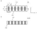
- (A) is a plan view showing the configuration of the wavelength conversion element according to the first embodiment, and (b) is a cross-sectional view taken along the line AA ′ of (a). It is a figure for demonstrating the method to manufacture a wavelength conversion element. It is a figure which shows an example of the relationship between the width H of a polarization inversion area
- FIG. 1A is a plan view showing the configuration of the wavelength conversion element 10 according to the first embodiment.
- FIG. 1B is a cross-sectional view taken along the line AA ′ of FIG.
- the wavelength conversion element 10 is formed using a ferroelectric crystal 100.
- the ferroelectric crystal 100 is provided with a plurality of domain-inverted regions 110 periodically along the first direction (X direction in FIG. 1A).
- the period L of the domain-inverted region 110 is 6.0 ⁇ m or more and 9.9 ⁇ m or less.
- the width H of the domain-inverted region 110 in the second direction (Y direction in FIG. 1A) perpendicular to the first direction is 0.01 mm or more and 1 mm or less. In this way, the quality of the wavelength conversion element is unlikely to deviate from the standard. Details will be described below.
- the ferroelectric crystal 100 is, for example, LiNbO 3 (lithium niobate) or LiTaO 3 (lithium tantalate) to which Mg (magnesium) is added, and the surface is a + Z plane.
- the thickness of the ferroelectric crystal 100 is, for example, not less than 0.2 mm and not more than 2.0 mm.
- the domain-inverted region 110 is repeatedly provided in the wavelength conversion element 10.
- the design value of the width W in the first direction of the domain-inverted region 110 is half the period L of the domain-inverted region 110. However, the width W is not less than 45% and not more than 55% of the period L due to variations caused by the manufacturing process.
- the period L of the domain-inverted region 110 is 6.0 ⁇ m or more and 9.9 ⁇ m or less. Therefore, the wavelength conversion element 10 functions as an element that converts incident light having a wavelength of 1020 nm to 1200 nm into outgoing light having a wavelength of 510 nm to 600 nm.
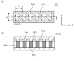
- FIG. 2 is a diagram for explaining a method of manufacturing the wavelength conversion element 10.
- 2A is a plan view
- FIG. 2B is a cross-sectional view taken along the line AA ′ of FIG. 2A.
- the manufacturing method of this wavelength conversion element 10 has the following processes. First, the first electrode 220 is disposed on the first surface (for example, the surface) of the ferroelectric crystal 100, and the second electrode 222 is disposed on the second surface (the surface opposite to the first surface) of the ferroelectric crystal 100. Place. The first electrode 220 is in contact only with the region of the first surface where the domain-inverted region 110 is formed. That is, the 1st electrode 220 is arrange
- the period of the contact portion is 6.0 ⁇ m or more and 9.9 ⁇ m or less.
- the width of the first electrode 220 in the second direction (the Y direction in FIG. 2A) is not less than 0.01 mm and not more than 1 mm.
- the domain-inverted region 110 is formed by applying a voltage between the first electrode 220 and the second electrode 222. Details will be described below.
- the second electrode 222 is formed on the second surface (the lower surface in the figure) of the ferroelectric crystal 100 by, for example, a sputtering method or a vacuum evaporation method.
- the second electrode 222 is, for example, an Al (aluminum) film or a Cr (chromium) film, and the thickness thereof is, for example, 0.5 ⁇ m.
- an insulating film 210 is formed on the first surface of the ferroelectric crystal 100, and the insulating film 210 is selectively removed. As a result, the region of the first surface of the ferroelectric crystal 100 where the polarization is not reversed is covered with the insulating film 210.
- the insulating film 210 is, for example, a photoresist film, but may be another insulating film.
- the first electrode 220 is formed on the first surface of the ferroelectric crystal 100 and on the insulating film 210.
- the method for forming the first electrode 220 is the same as the method for forming the second electrode 222.
- a voltage is applied between the first electrode 220 and the second electrode 222.
- the domain-inverted region 110 is formed in the ferroelectric crystal 100.
- the first electrode 220 and the second electrode 222 are removed, and the insulating film 210 is further removed.
- the crystal composition and crystal structure of the ferroelectric crystal 100 are not only uniform, but also the first electrode.
- the structures of the 220 and the second electrode 222 are preferably uniform. The inventor paid attention to this point and assumed that the width H of the first electrode 220 in the second direction affects the polarization inversion property.
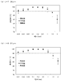
- 3A and 3B show an example of the relationship between the width H of the domain-inverted region 110, that is, the width of the portion of the first electrode 220 that is in contact with the ferroelectric crystal 100 and the yield of the wavelength conversion element 10. Is shown.
- L 7.38 ⁇ m
- L 9.52 ⁇ m.
- the ferroelectric crystal 100 LiNbO 3 having a thickness of 0.5 mm and added with MgO was used. Five samples were prepared for each H.
- the ratio of the area of the domain-inverted region 110 to the contact portion between the first electrode 220 and the ferroelectric crystal 100 is defined as the yield. That is, when all of the contact portions described above are polarized, the yield is 100%.
- the region serving as the domain-inverted region 110 can be confirmed by wet etching the ferroelectric crystal 100.
- the width H when the width H is 2 mm or less, the non-polarized region (hereinafter referred to as an uninverted region) decreases, and the yield of the polarized region 110 is increased. Improved. In particular, when the width H is 1 mm or less, the yield is greatly improved and exceeds 95%. Further, when the width H was 0.5 mm or less, no uninverted region was generated. This tendency was confirmed up to a width H of 0.1 mm.
- a plurality of samples are prepared by changing the width H of the portion of the first electrode 220 that is in contact with the ferroelectric crystal 100. Yes. Then, using the manufactured sample, the relationship between the yield of the domain-inverted region 110 and the width H is examined. Based on the result, the width H of the portion of the first electrode 220 that contacts the ferroelectric crystal 100 is determined.
- the yield of the wavelength conversion element 10 is improved when the width H is 0.01 mm or more and 1 mm or less.
- the width H is 0.02 mm or more and 0.5 mm or less, the yield of the wavelength conversion element 10 is further improved.
- the width H is set to 0.1 mm or more and 0.5 mm or less, the yield of the wavelength conversion element 10 becomes particularly high.
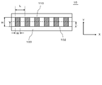
- FIG. 4 is a plan view showing the configuration of the wavelength conversion element 10 according to the second embodiment.
- the wavelength conversion element 10 according to the present embodiment has the same configuration as the wavelength conversion element 10 according to the first embodiment, except that the waveguide 102 is provided.
- the waveguide 102 extends in the first direction (X direction in FIG. 4).
- the waveguide 102 is either a ridge type or a buried type.
- the domain-inverted region 110 is provided in the waveguide 102.
- FIG. 5 is a diagram illustrating a configuration of a light source device according to the third embodiment.
- the light source device includes a wavelength conversion element 10 and a light source 20.
- the configuration of the wavelength conversion element 10 is the same as that of the first embodiment or the second embodiment.
- the light source 20 generates laser light having a wavelength of 1020 nm to 1200 nm.
- the light source 20 generates, for example, a super continuum laser.
- the light source 20 may be a laser diode that emits a single wavelength.
- the light emitted from the light source 20 enters the wavelength conversion element 10.
- the wavelength conversion element 10 converts the wavelength of incident light and emits it.
- the wavelength of the emitted light is 510 nm or more and 1200 nm or less.
- the light emitted from the light source 20 may be guided to the wavelength conversion element 10 using an optical fiber, or may be guided by an optical component such as a mirror.
- the light source device further includes a temperature adjustment element 30, a heat conduction unit 32, a temperature detection unit 40, and a control unit 50.
- the temperature adjustment element 30 is in contact with the wavelength conversion element 10 via the heat conducting unit 32.
- the temperature adjustment element 30 has at least one of a heat generation function and a heat absorption function.
- the temperature adjustment element 30 has, for example, at least one of a heater and a Peltier element.
- the heat conducting unit 32 is formed of a material having high heat conductivity such as Cu (copper).
- the temperature detection unit 40 detects the temperature of the wavelength conversion element 10.
- the control unit 50 controls the temperature adjustment element 30 based on the detection result of the temperature detection unit 40. That is, the control unit 50 controls the temperature adjustment element 30 so that the temperature of the wavelength conversion element 10 falls within a desired range. This desired temperature is, for example, 25 ° C. or more and 80 ° C. or less.
- the yield of the wavelength conversion element 10 is high. For this reason, the manufacturing cost of the light source device can be reduced. Moreover, since the light source device includes the temperature adjustment element 30, the temperature detection unit 40, and the control unit 50, the temperature of the wavelength conversion element 10 can be controlled within a desired range. For this reason, the wavelength conversion efficiency of the wavelength conversion element 10 can be maintained at a high value.
- FIG. 6 is a diagram illustrating a configuration of a light source device according to the fourth embodiment.
- the light source device has the same configuration as that of the light source device according to the third embodiment except that an intensity detection unit 42 is provided instead of the temperature detection unit 40.
- the light source 20 is an excitation light source having a narrow wavelength width such as a laser diode.
- the intensity detector 42 detects the intensity of the light emitted from the wavelength conversion element 10. Then, the control unit 50 controls the temperature adjustment element 30 based on the detection result of the intensity detection unit 42. Specifically, the control unit 50 controls the temperature adjustment element 30 so that the detection result of the intensity detection unit 42 is high (preferably maximized).
- the light source device may include a branching unit 60.
- the branching unit 60 branches a part of the light emitted from the wavelength conversion element 10 and inputs the branched light to the intensity detection unit 42.
- Example 1 A plurality of wavelength conversion elements 10 shown in the second embodiment were produced.
- the period of the domain-inverted region 110 was as shown in Table 1. And five samples were produced in each period. Then, the yield of the domain-inverted region 110 was measured. The definition of the yield is the same as the yield shown in FIG.
- the yield of the domain-inverted region 110 was 95% under all conditions shown in Table 1. Thereby, it was shown that the yield of the wavelength conversion element 10 is improved when the period L is 6.0 ⁇ m or more and 9.9 ⁇ m or less.
- Example 2 Using the wavelength conversion element 10 produced in Example 1, the light source device shown in the third embodiment was produced.
- the wavelength of the light emitted from the light source 20 was 1020 nm or more and 1200 nm or less.
- Table 2 shows a design value and a measured value of the wavelength of light emitted from the wavelength conversion element 10.
- the control unit 50 controls the temperature of the wavelength conversion element 10 to 40 ° C.
- the wavelength of the light emitted from the wavelength conversion element 10 was almost the same as the design value.
Landscapes
- Physics & Mathematics (AREA)
- Nonlinear Science (AREA)
- General Physics & Mathematics (AREA)
- Optics & Photonics (AREA)
- Optical Modulation, Optical Deflection, Nonlinear Optics, Optical Demodulation, Optical Logic Elements (AREA)
Abstract
波長変換素子(10)は、強誘電体結晶(100)を用いて形成されている。強誘電体結晶(100)には、複数の分極反転領域(110)が、第1の方向(X方向)に沿って周期的に設けられている。分極反転領域(110)の周期Lは、6.0μm以上9.9μm以下である。そして、第1の方向に直交する第2の方向(Y方向)における分極反転領域(110)の幅Hは、0.01mm以上1mm以下である。分極反転領域(110)の幅は、0.1mm以上0.5mm以下であるのが好ましい。
Description
本発明は、強誘電体結晶に分極反転構造を設けた波長変換素子、光源装置、及び波長変換素子の製造方法に関する。
光の波長を変換する波長変換素子の一つに、擬似位相整合を用いるものがある。この波長変換素子は、強誘電体結晶に分極反転領域を周期的に設けたものである。分極反転領域は、強誘電体結晶の一面のうち分極反転させたい領域に第1電極を接触させ、かつ強誘電体結晶の反対面の全面に第2電極を接触させ、第1電極及び第2電極の間に電圧を印加することにより形成される。特許文献1には、この第1電極の、分極反転周期に垂直な方向における長さを、強誘電体結晶の厚さの2倍以下にすることが記載されている。
波長変換素子の品質を向上させるためには、分極反転領域を設計通りに形成する必要がある。しかし、本発明者が検討した結果、第1電極が接していても分極反転されない部分が発生する場合があった。このような場合、波長変換素子の品質が基準から外れる場合が発生し、その結果、波長変換素子の歩留まりが低下してしまう。
本発明は上記事情に鑑みてなされたものであり、その目的とするところは、波長変換素子の歩留まりを高めることにある。
本発明によれば、波長変換素子は、強誘電体結晶を備えている。この強誘電体結晶は、第1の方向に沿って周期的に設けられた複数の分極反転領域を有している。分極反転領域の周期は6.0μm以上9.9μm以下である。また、第1の方向に直交する第2の方向における分極反転領域の幅は、0.01mm以上1mm以下である。
本発明によれば、光源装置は、波長が1020nm以上1200nm以下のレーザ光を発生する光源と、上記した波長変換素子とを有する。
本発明に係る波長変換素子の製造方法は、以下の工程を有している。まず、強誘電体結晶の第1面に位置していて分極反転される第1領域上に、複数の第1電極を第1の方向に沿って周期的に配置するとともに、強誘電体結晶の第1面の反対面である第2面上に第2電極を配置する。次いで、第1電極と第2電極の間に電圧を印加することにより分極反転領域を形成する。複数の第1電極の周期は、6.0μm以上9.9μm以下である。また、第1の方向に直交する第2の方向における第1電極の幅は、0.01mm以上1mm以下である。
本発明に係る波長変換素子の製造方法は、第1工程及び第2工程を繰り返すことにより、複数の波長変換素子を製造するものである。第1工程では、強誘電体結晶の第1面上に、第1電極を、当該第1電極と第1面の接触部分が周期的になるように配置するとともに、強誘電体結晶の第1面の反対面である第2面上に第2電極を配置する。第2工程では、第1電極と第2電極の間に電圧を印加することにより、分極反転領域を形成する。そして第1工程及び第2工程を繰り返す前に、第1の方向に直交する第2の方向における第1電極の幅を変えつつ、波長変換素子の試料を複数作製する。そして、複数の試料における分極反転領域の歩留まりを調べることにより、第1工程で用いる第1電極の幅を決定する。
本発明によれば、波長変換素子の歩留まりを高めることができる。
上述した目的、およびその他の目的、特徴および利点は、以下に述べる好適な実施の形態、およびそれに付随する以下の図面によってさらに明らかになる。
以下、本発明の実施の形態について、図面を用いて説明する。尚、すべての図面において、同様な構成要素には同様の符号を付し、適宜説明を省略する。
(第1の実施形態)
図1(a)は、第1の実施形態に係る波長変換素子10の構成を示す平面図である。図1(b)は、図1(a)のA-A´断面図である。波長変換素子10は、強誘電体結晶100を用いて形成されている。強誘電体結晶100には、複数の分極反転領域110が、第1の方向(図1(a)のX方向)に沿って周期的に設けられている。分極反転領域110の周期Lは、6.0μm以上9.9μm以下である。そして、第1の方向に直交する第2の方向(図1(a)のY方向)における分極反転領域110の幅Hは、0.01mm以上1mm以下である。このようにすると、波長変換素子の品質は、基準から外れにくくなる。以下、詳細に説明する。
図1(a)は、第1の実施形態に係る波長変換素子10の構成を示す平面図である。図1(b)は、図1(a)のA-A´断面図である。波長変換素子10は、強誘電体結晶100を用いて形成されている。強誘電体結晶100には、複数の分極反転領域110が、第1の方向(図1(a)のX方向)に沿って周期的に設けられている。分極反転領域110の周期Lは、6.0μm以上9.9μm以下である。そして、第1の方向に直交する第2の方向(図1(a)のY方向)における分極反転領域110の幅Hは、0.01mm以上1mm以下である。このようにすると、波長変換素子の品質は、基準から外れにくくなる。以下、詳細に説明する。
強誘電体結晶100は、例えばMg(マグネシウム)が添加されたLiNbO3(ニオブ酸リチウム)又はLiTaO3(タンタル酸リチウム)であり、表面が+Z面となっている。強誘電体結晶100の厚さは、例えば0.2mm以上2.0mm以下である。平面視において、分極反転領域110は、波長変換素子10に繰り返し設けられている。分極反転領域110の第1の方向の幅Wの設計値は、分極反転領域110の周期Lの半分である。ただし、製造プロセスに起因したばらつきにより、幅Wは、周期Lの45%以上55%以下となっている。
本実施形態において、分極反転領域110の周期Lは、6.0μm以上9.9μm以下である。このため、波長変換素子10は、波長が1020nm以上1200nm以下の入射光を、波長が510nm以上600nm以下の出射光に変換する素子として機能する。
図2は、波長変換素子10を製造する方法を説明するための図である。図2(a)は平面図であり、図2(b)は図2(a)のA-A´断面図である。この波長変換素子10の製造方法は、以下の工程を有している。まず、強誘電体結晶100の第1面(例えば表面)に第1電極220を配置すると共に、強誘電体結晶100の第2面(第1面とは反対側の面)に第2電極222を配置する。第1電極220は、第1面のうち分極反転領域110が形成される領域にのみ接触している。すなわち第1電極220は、第1面との接触部分が周期的になるように配置されている。このとき、接触部分の周期は、6.0μm以上9.9μm以下である。また、第2の方向(図2(a)のY方向)における第1電極220の幅は、0.01mm以上1mm以下である。次いで、第1電極220と第2電極222の間に電圧を印加することにより、分極反転領域110を形成する。以下、詳細に説明する。
まず、強誘電体結晶100の第2面(本図では下面)上に、第2電極222を、例えばスパッタリング法又は真空蒸着法により形成する。第2電極222は、例えばAl(アルミニウム)膜またはCr(クロム)膜であり、その厚さは例えば0.5μmである。
次いで、強誘電体結晶100の第1面上に、絶縁膜210を形成し、絶縁膜210を選択的に除去する。これにより、強誘電体結晶100の第1面のうち分極反転されない領域は、絶縁膜210で被覆される。絶縁膜210は、例えばフォトレジスト膜であるが、他の絶縁膜であってもよい。
次いで、強誘電体結晶100の第1面上及び絶縁膜210上に、第1電極220を形成する。第1電極220の形成方法は、第2電極222の形成方法と同様である。次いで、第1電極220と第2電極222の間に電圧を印加する。これにより、強誘電体結晶100には分極反転領域110が形成される。その後、第1電極220及び第2電極222を除去し、さらに絶縁膜210を除去する。
次に、本実施形態の効果について説明する。電圧印加法を用いて強誘電体結晶100に分極反転領域110を精度良く形成するためには、強誘電体結晶100の結晶組成や結晶構造が均一であることが望ましいだけでなく、第1電極220及び第2電極222の構造も均一であることが望ましい。本発明者はこの点に着目し、第2方向における第1電極220の幅Hが分極反転性を左右すると仮定した。
図3(a)、(b)は、分極反転領域110の幅H、すなわち第1電極220のうち強誘電体結晶100に接触している部分の幅と波長変換素子10の歩留まりの関係の一例を示している。図3(a)では、L=7.38μmとして、図3(b)に示す例ではL=9.52μmとした。強誘電体結晶100には、厚さが0.5mmであり、MgOが添加されたLiNbO3を用いた。各Hについて試料は5つ作製した。図3において、第1電極220と強誘電体結晶100の接触部分に対する、分極反転領域110の面積の割合を、歩留まりとして定義した。すなわち、上記した接触部分の全てが分極反転した場合、歩留まりは100%となる。なお、分極反転領域110となっている領域は、強誘電体結晶100をウェットエッチングすることにより、確認できる。
図3(a),(b)のいずれの例においても、幅Hが2mm以下になると、分極反転していない領域(以下、未反転領域と記載)が減少し、分極反転領域110の歩留まりが向上した。特に幅Hが1mm以下の場合、歩留まりは大きく向上し、95%を超えている。さらに幅Hが0.5mm以下になると、未反転領域は発生しなかった。この傾向は、幅Hが0.1mmまで確認できた。
幅Hが0.05mm以下になると、未反転領域が再び発生し、分極反転領域110の歩留まりは少し減少した。ただし、幅が0.01mmの場合においても、歩留まりは95%以上であった。
このように、本実施形態においては、波長変換素子10を製造する前に、第1電極220のうち強誘電体結晶100に接触している部分の幅Hを変えて複数の試料を作製している。そしてその作製した試料を用いて、分極反転領域110の歩留まりと幅Hの関係を調べている。そしてその結果に基づいて、第1電極220のうち強誘電体結晶100に接触する部分の幅Hを決めている。
そして、分極反転領域110の周期Lが6.0μm以上9.9μm以下である場合において、幅Hを0.01mm以上1mm以下にすると、波長変換素子10の歩留まりは向上する。幅Hを0.02mm以上0.5mm以下にすると、波長変換素子10の歩留まりはさらに向上する。さらに幅Hを0.1mm以上0.5mm以下にすると、波長変換素子10の歩留まりは特に高くなる。
(第2の実施形態)
図4は、第2の実施形態に係る波長変換素子10の構成を示す平面図である。本実施形態に係る波長変換素子10は、導波路102を有している点を除いて、第1の実施形態に係る波長変換素子10と同様の構成である。
図4は、第2の実施形態に係る波長変換素子10の構成を示す平面図である。本実施形態に係る波長変換素子10は、導波路102を有している点を除いて、第1の実施形態に係る波長変換素子10と同様の構成である。
詳細には、導波路102は、第1の方向(図4のX方向)に延伸している。導波路102は、リッジ型または埋め込み型のいずれかである。そして分極反転領域110は、導波路102に設けられている。
本実施形態によっても、第1の実施形態と同様の効果を得ることができる。
(第3の実施形態)
図5は、第3の実施形態に係る光源装置の構成を示す図である。この光源装置は、波長変換素子10及び光源20を有している。波長変換素子10の構成は、第1の実施形態又は第2の実施形態と同様である。光源20は、波長が1020nm以上1200nm以下のレーザ光を発生する。光源20は、例えばスーパーコンティニュームレーザーを発生する。また光源20は、単一波長を出射するレーザダイオードであっても良い。光源20から出射した光は、波長変換素子10に入射する。波長変換素子10は、入射した光を波長変換して、出射する。出射する光の波長は、510nm以上1200nm以下である。なお、光源20から出射した光は、光ファイバを用いて波長変換素子10に導光されてもよいし、ミラーなどの光学部品によって導光されても良い。
図5は、第3の実施形態に係る光源装置の構成を示す図である。この光源装置は、波長変換素子10及び光源20を有している。波長変換素子10の構成は、第1の実施形態又は第2の実施形態と同様である。光源20は、波長が1020nm以上1200nm以下のレーザ光を発生する。光源20は、例えばスーパーコンティニュームレーザーを発生する。また光源20は、単一波長を出射するレーザダイオードであっても良い。光源20から出射した光は、波長変換素子10に入射する。波長変換素子10は、入射した光を波長変換して、出射する。出射する光の波長は、510nm以上1200nm以下である。なお、光源20から出射した光は、光ファイバを用いて波長変換素子10に導光されてもよいし、ミラーなどの光学部品によって導光されても良い。
本実施形態において、光源装置は、さらに温度調節素子30、熱伝導部32、温度検出部40、及び制御部50を有している。温度調節素子30は、熱伝導部32を介して波長変換素子10に接触している。温度調節素子30は、発熱機能及び吸熱機能の少なくとも一方を有している。温度調節素子30は、例えばヒータ及びペルチェ素子の少なくとも一方を有している。熱伝導部32は、例えばCu(銅)など、熱伝導率が高い物質により形成されている。温度検出部40は、波長変換素子10の温度を検出する。制御部50は、温度検出部40の検出結果に基づいて、温度調節素子30を制御する。すなわち制御部50は、温度調節素子30を制御することにより、波長変換素子10の温度が所望の範囲内となるようにする。この所望の温度は、例えば25℃以上80℃以下である。
本実施形態によれば、波長変換素子10の歩留まりは高い。このため、光源装置の製造コストを低くすることができる。また、光源装置は、温度調節素子30、温度検出部40、及び制御部50を備えているため、波長変換素子10の温度を所望の範囲に制御することができる。このため、波長変換素子10の波長変換効率を高い値に維持することができる。
(第4の実施形態)
図6は、第4の実施形態に係る光源装置の構成を示す図である。この光源装置は、温度検出部40の代わりに強度検出部42を備えている点を除いて、第3の実施形態に係る光源装置と同様の構成である。なお、本実施形態において、光源20は、レーザダイオードなどの波長幅が狭い励起光源である。
図6は、第4の実施形態に係る光源装置の構成を示す図である。この光源装置は、温度検出部40の代わりに強度検出部42を備えている点を除いて、第3の実施形態に係る光源装置と同様の構成である。なお、本実施形態において、光源20は、レーザダイオードなどの波長幅が狭い励起光源である。
強度検出部42は、波長変換素子10から出射した光の強度を検出する。そして制御部50は、強度検出部42の検出結果に基づいて、温度調節素子30を制御する。具体的には、制御部50は、強度検出部42の検出結果が高くなる(好ましくは最大となる)ように、温度調節素子30を制御する。
なお、図7に示すように、本実施形態に係る光源装置は、分岐部60を備えていても良い。分岐部60は、波長変換素子10から出射した光の一部を分岐して、強度検出部42に入力する。
本実施形態によっても、第3の実施形態と同様の効果を得ることができる。
(実施例1)
第2の実施形態に示した波長変換素子10を複数作製した。この実施例において、分極反転領域110の周期は、表1に示す通りとした。そして、各周期において、試料を5つ作製した。そして、分極反転領域110の歩留まりを測定した。この歩留まりの定義は、図3に示した歩留まりと同じである。
第2の実施形態に示した波長変換素子10を複数作製した。この実施例において、分極反転領域110の周期は、表1に示す通りとした。そして、各周期において、試料を5つ作製した。そして、分極反転領域110の歩留まりを測定した。この歩留まりの定義は、図3に示した歩留まりと同じである。

本実施例では、表1に示した全ての条件において、分極反転領域110の歩留まりが95%であった。これにより、周期Lが6.0μm以上9.9μm以下である場合において、波長変換素子10の歩留まりは向上することが示された。
(実施例2)
実施例1で作製した波長変換素子10を用いて、第3の実施形態に示した光源装置を作製した。光源20が出射する光の波長は、1020nm以上1200nm以下であった。表2に、波長変換素子10が出射する光の波長の設計値と、実測値をそれぞれ示す。なお、本実施例において、制御部50は波長変換素子10の温度を40℃に制御した。
実施例1で作製した波長変換素子10を用いて、第3の実施形態に示した光源装置を作製した。光源20が出射する光の波長は、1020nm以上1200nm以下であった。表2に、波長変換素子10が出射する光の波長の設計値と、実測値をそれぞれ示す。なお、本実施例において、制御部50は波長変換素子10の温度を40℃に制御した。

表2に示すように、全ての試料において、波長変換素子10が出射する光の波長は、設計値とほぼ同じであった。
以上、図面を参照して本発明の実施形態及び実施例について述べたが、これらは本発明の例示であり、上記以外の様々な構成を採用することもできる。
この出願は、2012年9月20日に出願された日本出願特願2012-206751を基礎とする優先権を主張し、その開示の全てをここに取り込む。
Claims (8)
- 強誘電体結晶と、
前記強誘電体結晶に、第1の方向に沿って周期的に設けられた複数の分極反転領域と、
を備え、
前記分極反転領域の周期が6.0μm以上9.9μm以下であり、
前記第1の方向に直交する第2の方向における前記分極反転領域の幅は、0.01mm以上1mm以下である波長変換素子。 - 請求項1に記載の波長変換素子において、
前記分極反転領域の幅は、0.1mm以上0.5mm以下である波長変換素子。 - 請求項1に記載の波長変換素子において、
前記強誘電体結晶に設けられ、前記第1の方向に沿って延伸する導波路を備え、
前記複数の分極反転領域は、前記導波路に設けられている波長変換素子。 - 波長が1020nm以上1200nm以下のレーザ光を発生する光源と、
前記光源から出射した光を波長変換する波長変換素子と、
を備え、
前記波長変換素子は、
強誘電体結晶と、
前記強誘電体結晶に、第1の方向に沿って周期的に設けられた複数の分極反転領域と、
を備え、
前記分極反転領域の周期が6.0μm以上9.9μm以下であり、
前記第1の方向に直交する第2の方向における前記分極反転領域の幅は、0.01mm以上1mm以下である光源装置。 - 請求項4に記載の光源装置において、
前記強誘電体結晶の温度を検出する温度検出部と、
前記温度検出部の検出結果に基づいて前記強誘電体結晶の温度を制御する制御部と、
を備える光源装置。 - 請求項4に記載の光源装置において、
前記波長変換素子から出射した光の強度を検出する強度検出部と、
前記強度検出部の検出結果に基づいて前記強誘電体結晶の温度を制御する制御部と、
を備える光源装置。 - 強誘電体結晶の第1面上に、第1電極を、当該第1電極と前記第1面の接触部分が周期的になるように配置するとともに、前記強誘電体結晶の前記第1面の反対面である第2面上に第2電極を配置する工程と、
前記第1電極と前記第2電極の間に電圧を印加することにより、分極反転領域を形成する工程と、
を備え、
前記接触部分の周期は、6.0μm以上9.9μm以下であり、
前記第1の方向に直交する第2の方向における前記第1電極の幅は、0.01mm以上1mm以下である波長変換素子の製造方法。 - 強誘電体結晶の第1面上に、第1電極を、当該第1電極と前記第1面の接触部分が周期的になるように配置するとともに、前記強誘電体結晶の前記第1面の反対面である第2面上に第2電極を配置する第1工程と、
前記第1電極と前記第2電極の間に電圧を印加することにより、分極反転領域を形成する第2工程と、
を備え、
前記第1工程及び前記第2工程を繰り返すことにより、複数の波長変換素子を製造し、
前記第1工程及び前記第2工程を繰り返す前に、
前記第1の方向に直交する第2の方向における前記第1電極の幅を変えつつ、前記波長変換素子の試料を複数作製し、
前記複数の試料における前記分極反転領域の歩留まりを調べることにより、前記第1工程で用いる前記第1電極の幅を決定する、波長変換素子の製造方法。
Applications Claiming Priority (2)
| Application Number | Priority Date | Filing Date | Title |
|---|---|---|---|
| JP2012206751A JP2014062960A (ja) | 2012-09-20 | 2012-09-20 | 波長変換素子、光源装置、及び波長変換素子の製造方法 |
| JP2012-206751 | 2012-09-20 |
Publications (1)
| Publication Number | Publication Date |
|---|---|
| WO2014045658A1 true WO2014045658A1 (ja) | 2014-03-27 |
Family
ID=50340989
Family Applications (1)
| Application Number | Title | Priority Date | Filing Date |
|---|---|---|---|
| PCT/JP2013/067312 Ceased WO2014045658A1 (ja) | 2012-09-20 | 2013-06-25 | 波長変換素子、光源装置、及び波長変換素子の製造方法 |
Country Status (3)
| Country | Link |
|---|---|
| JP (1) | JP2014062960A (ja) |
| TW (1) | TW201413359A (ja) |
| WO (1) | WO2014045658A1 (ja) |
Cited By (2)
| Publication number | Priority date | Publication date | Assignee | Title |
|---|---|---|---|---|
| JP2016200642A (ja) * | 2015-04-07 | 2016-12-01 | 富士電機株式会社 | 光源装置及び波長変換方法 |
| US11460752B2 (en) * | 2020-03-13 | 2022-10-04 | Fujitsu Limited | Wavelength conversion device and wavelength conversion method |
Families Citing this family (3)
| Publication number | Priority date | Publication date | Assignee | Title |
|---|---|---|---|---|
| WO2019156177A1 (ja) * | 2018-02-08 | 2019-08-15 | 住友電気工業株式会社 | 波長変換光デバイスおよび波長変換光デバイスの製造方法 |
| CN108511918B (zh) * | 2018-03-13 | 2020-08-28 | 东北石油大学 | 基于超材料的电磁波非对称传输控制器 |
| WO2020255341A1 (ja) * | 2019-06-20 | 2020-12-24 | 日本電信電話株式会社 | 波長変換装置 |
Citations (9)
| Publication number | Priority date | Publication date | Assignee | Title |
|---|---|---|---|---|
| JPS49102366A (ja) * | 1973-01-31 | 1974-09-27 | ||
| JPS58138920U (ja) * | 1982-03-12 | 1983-09-19 | 日本電気株式会社 | 自動チユ−ニングshg装置 |
| JPH04310929A (ja) * | 1991-04-09 | 1992-11-02 | Ricoh Co Ltd | 光第二高調波発生素子 |
| JPH04335328A (ja) * | 1991-05-10 | 1992-11-24 | Hitachi Ltd | 第2高調波発生素子の製造方法 |
| JPH0777712A (ja) * | 1993-09-10 | 1995-03-20 | Sony Corp | 非線形光学材料に対する局所分極制御方法 |
| JPH09292637A (ja) * | 1996-04-26 | 1997-11-11 | Kyocera Corp | 第2高調波発生素子 |
| JPH09304800A (ja) * | 1996-03-12 | 1997-11-28 | Matsushita Electric Ind Co Ltd | 光波長変換素子および分極反転の製造方法 |
| JP2001109028A (ja) * | 1999-10-06 | 2001-04-20 | Mitsubishi Cable Ind Ltd | 分極反転構造の作製方法 |
| JP2009139395A (ja) * | 2007-12-03 | 2009-06-25 | Mitsubishi Electric Corp | 波長変換レーザ光源 |
-
2012
- 2012-09-20 JP JP2012206751A patent/JP2014062960A/ja active Pending
-
2013
- 2013-06-25 WO PCT/JP2013/067312 patent/WO2014045658A1/ja not_active Ceased
- 2013-09-17 TW TW102133658A patent/TW201413359A/zh unknown
Patent Citations (9)
| Publication number | Priority date | Publication date | Assignee | Title |
|---|---|---|---|---|
| JPS49102366A (ja) * | 1973-01-31 | 1974-09-27 | ||
| JPS58138920U (ja) * | 1982-03-12 | 1983-09-19 | 日本電気株式会社 | 自動チユ−ニングshg装置 |
| JPH04310929A (ja) * | 1991-04-09 | 1992-11-02 | Ricoh Co Ltd | 光第二高調波発生素子 |
| JPH04335328A (ja) * | 1991-05-10 | 1992-11-24 | Hitachi Ltd | 第2高調波発生素子の製造方法 |
| JPH0777712A (ja) * | 1993-09-10 | 1995-03-20 | Sony Corp | 非線形光学材料に対する局所分極制御方法 |
| JPH09304800A (ja) * | 1996-03-12 | 1997-11-28 | Matsushita Electric Ind Co Ltd | 光波長変換素子および分極反転の製造方法 |
| JPH09292637A (ja) * | 1996-04-26 | 1997-11-11 | Kyocera Corp | 第2高調波発生素子 |
| JP2001109028A (ja) * | 1999-10-06 | 2001-04-20 | Mitsubishi Cable Ind Ltd | 分極反転構造の作製方法 |
| JP2009139395A (ja) * | 2007-12-03 | 2009-06-25 | Mitsubishi Electric Corp | 波長変換レーザ光源 |
Cited By (2)
| Publication number | Priority date | Publication date | Assignee | Title |
|---|---|---|---|---|
| JP2016200642A (ja) * | 2015-04-07 | 2016-12-01 | 富士電機株式会社 | 光源装置及び波長変換方法 |
| US11460752B2 (en) * | 2020-03-13 | 2022-10-04 | Fujitsu Limited | Wavelength conversion device and wavelength conversion method |
Also Published As
| Publication number | Publication date |
|---|---|
| JP2014062960A (ja) | 2014-04-10 |
| TW201413359A (zh) | 2014-04-01 |
Similar Documents
| Publication | Publication Date | Title |
|---|---|---|
| Shi et al. | Efficient photon-pair generation in layer-poled lithium niobate nanophotonic waveguides | |
| Chauvet et al. | High efficiency frequency doubling in fully diced LiNbO3 ridge waveguides on silicon | |
| Xiong et al. | Active silicon integrated nanophotonics: ferroelectric BaTiO3 devices | |
| US20190383982A1 (en) | Metasurface on optical fiber and related method | |
| Degl’Innocenti et al. | Low-bias terahertz amplitude modulator based on split-ring resonators and graphene | |
| WO2014045658A1 (ja) | 波長変換素子、光源装置、及び波長変換素子の製造方法 | |
| JP6136666B2 (ja) | 光導波路および電気光学デバイス | |
| Tang et al. | Quasi-phase-matching enabled by van der Waals stacking | |
| CN1213436A (zh) | 光学晶体的极化方法和配置 | |
| Shin et al. | Enhanced Pockels effect in AlN microring resonator modulators based on AlGaN/AlN multiple quantum wells | |
| US12436442B2 (en) | Waveguide device, optical scanning device and optical modulation device | |
| Heidari et al. | Design and analysis of a polarization-insensitive VO2/graphene optical modulator using a 3D heat transfer method | |
| Rao et al. | Experimental characterization of the thermo-optic coefficient vs. temperature for 4H-SiC and GaN semiconductors at the wavelength of 632 nm | |
| Liu et al. | Bright multicolored photoluminescence of hybrid graphene/silicon optoelectronics | |
| Zhang et al. | 3D ultra-broadband optically dispersive microregions in lithium niobate | |
| Ding et al. | Gate‐tunable graphene optical modulator on fiber tip: design and demonstration | |
| CN101535887B (zh) | 光波导基板的制造方法 | |
| JP6774372B2 (ja) | 光学素子 | |
| US12436336B2 (en) | Optical scanning element | |
| JP2009271496A (ja) | 光機能素子の製造方法 | |
| JP2009169344A (ja) | 波長変換素子 | |
| Chauvet et al. | LiNbO3 ridge waveguides realized by precision dicing on silicon for high efficiency second harmonic generation | |
| JP7846421B2 (ja) | 波長変換素子の製造方法 | |
| JP2002250948A (ja) | 分極反転構造素子 | |
| JP6347486B2 (ja) | 光能動素子 |
Legal Events
| Date | Code | Title | Description |
|---|---|---|---|
| 121 | Ep: the epo has been informed by wipo that ep was designated in this application |
Ref document number: 13839245 Country of ref document: EP Kind code of ref document: A1 |
|
| NENP | Non-entry into the national phase |
Ref country code: DE |
|
| 122 | Ep: pct application non-entry in european phase |
Ref document number: 13839245 Country of ref document: EP Kind code of ref document: A1 |