WO2014042049A1 - 半導体リングレーザー装置 - Google Patents
半導体リングレーザー装置 Download PDFInfo
- Publication number
- WO2014042049A1 WO2014042049A1 PCT/JP2013/073778 JP2013073778W WO2014042049A1 WO 2014042049 A1 WO2014042049 A1 WO 2014042049A1 JP 2013073778 W JP2013073778 W JP 2013073778W WO 2014042049 A1 WO2014042049 A1 WO 2014042049A1
- Authority
- WO
- WIPO (PCT)
- Prior art keywords
- semiconductor
- semiconductor substrate
- ring
- laser device
- optical waveguide
- Prior art date
- Legal status (The legal status is an assumption and is not a legal conclusion. Google has not performed a legal analysis and makes no representation as to the accuracy of the status listed.)
- Ceased
Links
Images


Classifications
-
- H—ELECTRICITY
- H01—ELECTRIC ELEMENTS
- H01S—DEVICES USING THE PROCESS OF LIGHT AMPLIFICATION BY STIMULATED EMISSION OF RADIATION [LASER] TO AMPLIFY OR GENERATE LIGHT; DEVICES USING STIMULATED EMISSION OF ELECTROMAGNETIC RADIATION IN WAVE RANGES OTHER THAN OPTICAL
- H01S5/00—Semiconductor lasers
- H01S5/10—Construction or shape of the optical resonator, e.g. extended or external cavity, coupled cavities, bent-guide, varying width, thickness or composition of the active region
- H01S5/1071—Ring-lasers
-
- G—PHYSICS
- G01—MEASURING; TESTING
- G01C—MEASURING DISTANCES, LEVELS OR BEARINGS; SURVEYING; NAVIGATION; GYROSCOPIC INSTRUMENTS; PHOTOGRAMMETRY OR VIDEOGRAMMETRY
- G01C19/00—Gyroscopes; Turn-sensitive devices using vibrating masses; Turn-sensitive devices without moving masses; Measuring angular rate using gyroscopic effects
- G01C19/58—Turn-sensitive devices without moving masses
- G01C19/64—Gyrometers using the Sagnac effect, i.e. rotation-induced shifts between counter-rotating electromagnetic beams
- G01C19/66—Ring laser gyrometers
- G01C19/661—Ring laser gyrometers details
-
- H—ELECTRICITY
- H01—ELECTRIC ELEMENTS
- H01S—DEVICES USING THE PROCESS OF LIGHT AMPLIFICATION BY STIMULATED EMISSION OF RADIATION [LASER] TO AMPLIFY OR GENERATE LIGHT; DEVICES USING STIMULATED EMISSION OF ELECTROMAGNETIC RADIATION IN WAVE RANGES OTHER THAN OPTICAL
- H01S3/00—Lasers, i.e. devices using stimulated emission of electromagnetic radiation in the infrared, visible or ultraviolet wave range
- H01S3/05—Construction or shape of optical resonators; Accommodation of active medium therein; Shape of active medium
- H01S3/08—Construction or shape of optical resonators or components thereof
- H01S3/081—Construction or shape of optical resonators or components thereof comprising three or more reflectors
- H01S3/083—Ring lasers
-
- H—ELECTRICITY
- H01—ELECTRIC ELEMENTS
- H01S—DEVICES USING THE PROCESS OF LIGHT AMPLIFICATION BY STIMULATED EMISSION OF RADIATION [LASER] TO AMPLIFY OR GENERATE LIGHT; DEVICES USING STIMULATED EMISSION OF ELECTROMAGNETIC RADIATION IN WAVE RANGES OTHER THAN OPTICAL
- H01S5/00—Semiconductor lasers
- H01S5/02—Structural details or components not essential to laser action
- H01S5/0206—Substrates, e.g. growth, shape, material, removal or bonding
- H01S5/021—Silicon based substrates
-
- H—ELECTRICITY
- H01—ELECTRIC ELEMENTS
- H01S—DEVICES USING THE PROCESS OF LIGHT AMPLIFICATION BY STIMULATED EMISSION OF RADIATION [LASER] TO AMPLIFY OR GENERATE LIGHT; DEVICES USING STIMULATED EMISSION OF ELECTROMAGNETIC RADIATION IN WAVE RANGES OTHER THAN OPTICAL
- H01S5/00—Semiconductor lasers
- H01S5/02—Structural details or components not essential to laser action
- H01S5/026—Monolithically integrated components, e.g. waveguides, monitoring photo-detectors, drivers
- H01S5/0261—Non-optical elements, e.g. laser driver components, heaters
-
- H—ELECTRICITY
- H01—ELECTRIC ELEMENTS
- H01S—DEVICES USING THE PROCESS OF LIGHT AMPLIFICATION BY STIMULATED EMISSION OF RADIATION [LASER] TO AMPLIFY OR GENERATE LIGHT; DEVICES USING STIMULATED EMISSION OF ELECTROMAGNETIC RADIATION IN WAVE RANGES OTHER THAN OPTICAL
- H01S5/00—Semiconductor lasers
- H01S5/02—Structural details or components not essential to laser action
- H01S5/026—Monolithically integrated components, e.g. waveguides, monitoring photo-detectors, drivers
- H01S5/0262—Photo-diodes, e.g. transceiver devices, bidirectional devices
- H01S5/0264—Photo-diodes, e.g. transceiver devices, bidirectional devices for monitoring the laser-output
-
- H—ELECTRICITY
- H01—ELECTRIC ELEMENTS
- H01S—DEVICES USING THE PROCESS OF LIGHT AMPLIFICATION BY STIMULATED EMISSION OF RADIATION [LASER] TO AMPLIFY OR GENERATE LIGHT; DEVICES USING STIMULATED EMISSION OF ELECTROMAGNETIC RADIATION IN WAVE RANGES OTHER THAN OPTICAL
- H01S5/00—Semiconductor lasers
- H01S5/06—Arrangements for controlling the laser output parameters, e.g. by operating on the active medium
- H01S5/068—Stabilisation of laser output parameters
- H01S5/0683—Stabilisation of laser output parameters by monitoring the optical output parameters
-
- H—ELECTRICITY
- H01—ELECTRIC ELEMENTS
- H01S—DEVICES USING THE PROCESS OF LIGHT AMPLIFICATION BY STIMULATED EMISSION OF RADIATION [LASER] TO AMPLIFY OR GENERATE LIGHT; DEVICES USING STIMULATED EMISSION OF ELECTROMAGNETIC RADIATION IN WAVE RANGES OTHER THAN OPTICAL
- H01S5/00—Semiconductor lasers
- H01S5/10—Construction or shape of the optical resonator, e.g. extended or external cavity, coupled cavities, bent-guide, varying width, thickness or composition of the active region
- H01S5/14—External cavity lasers
-
- H—ELECTRICITY
- H01—ELECTRIC ELEMENTS
- H01S—DEVICES USING THE PROCESS OF LIGHT AMPLIFICATION BY STIMULATED EMISSION OF RADIATION [LASER] TO AMPLIFY OR GENERATE LIGHT; DEVICES USING STIMULATED EMISSION OF ELECTROMAGNETIC RADIATION IN WAVE RANGES OTHER THAN OPTICAL
- H01S5/00—Semiconductor lasers
- H01S5/20—Structure or shape of the semiconductor body to guide the optical wave ; Confining structures perpendicular to the optical axis, e.g. index or gain guiding, stripe geometry, broad area lasers, gain tailoring, transverse or lateral reflectors, special cladding structures, MQW barrier reflection layers
- H01S5/2004—Confining in the direction perpendicular to the layer structure
- H01S5/2018—Optical confinement, e.g. absorbing-, reflecting- or waveguide-layers
- H01S5/2031—Optical confinement, e.g. absorbing-, reflecting- or waveguide-layers characterized by special waveguide layers, e.g. asymmetric waveguide layers or defined bandgap discontinuities
-
- H—ELECTRICITY
- H01—ELECTRIC ELEMENTS
- H01S—DEVICES USING THE PROCESS OF LIGHT AMPLIFICATION BY STIMULATED EMISSION OF RADIATION [LASER] TO AMPLIFY OR GENERATE LIGHT; DEVICES USING STIMULATED EMISSION OF ELECTROMAGNETIC RADIATION IN WAVE RANGES OTHER THAN OPTICAL
- H01S5/00—Semiconductor lasers
- H01S5/30—Structure or shape of the active region; Materials used for the active region
- H01S5/305—Structure or shape of the active region; Materials used for the active region characterised by the doping materials used in the laser structure
-
- H—ELECTRICITY
- H01—ELECTRIC ELEMENTS
- H01S—DEVICES USING THE PROCESS OF LIGHT AMPLIFICATION BY STIMULATED EMISSION OF RADIATION [LASER] TO AMPLIFY OR GENERATE LIGHT; DEVICES USING STIMULATED EMISSION OF ELECTROMAGNETIC RADIATION IN WAVE RANGES OTHER THAN OPTICAL
- H01S5/00—Semiconductor lasers
- H01S5/30—Structure or shape of the active region; Materials used for the active region
- H01S5/305—Structure or shape of the active region; Materials used for the active region characterised by the doping materials used in the laser structure
- H01S5/3054—Structure or shape of the active region; Materials used for the active region characterised by the doping materials used in the laser structure p-doping
-
- H—ELECTRICITY
- H01—ELECTRIC ELEMENTS
- H01S—DEVICES USING THE PROCESS OF LIGHT AMPLIFICATION BY STIMULATED EMISSION OF RADIATION [LASER] TO AMPLIFY OR GENERATE LIGHT; DEVICES USING STIMULATED EMISSION OF ELECTROMAGNETIC RADIATION IN WAVE RANGES OTHER THAN OPTICAL
- H01S3/00—Lasers, i.e. devices using stimulated emission of electromagnetic radiation in the infrared, visible or ultraviolet wave range
- H01S3/05—Construction or shape of optical resonators; Accommodation of active medium therein; Shape of active medium
- H01S3/06—Construction or shape of active medium
- H01S3/07—Construction or shape of active medium consisting of a plurality of parts, e.g. segments
-
- H—ELECTRICITY
- H01—ELECTRIC ELEMENTS
- H01S—DEVICES USING THE PROCESS OF LIGHT AMPLIFICATION BY STIMULATED EMISSION OF RADIATION [LASER] TO AMPLIFY OR GENERATE LIGHT; DEVICES USING STIMULATED EMISSION OF ELECTROMAGNETIC RADIATION IN WAVE RANGES OTHER THAN OPTICAL
- H01S5/00—Semiconductor lasers
- H01S5/04—Processes or apparatus for excitation, e.g. pumping, e.g. by electron beams
- H01S5/042—Electrical excitation ; Circuits therefor
- H01S5/0425—Electrodes, e.g. characterised by the structure
- H01S5/04256—Electrodes, e.g. characterised by the structure characterised by the configuration
-
- H—ELECTRICITY
- H01—ELECTRIC ELEMENTS
- H01S—DEVICES USING THE PROCESS OF LIGHT AMPLIFICATION BY STIMULATED EMISSION OF RADIATION [LASER] TO AMPLIFY OR GENERATE LIGHT; DEVICES USING STIMULATED EMISSION OF ELECTROMAGNETIC RADIATION IN WAVE RANGES OTHER THAN OPTICAL
- H01S5/00—Semiconductor lasers
- H01S5/40—Arrangement of two or more semiconductor lasers, not provided for in groups H01S5/02 - H01S5/30
- H01S5/4006—Injection locking
Definitions
- the present invention relates to a semiconductor ring laser device that can constitute a ring laser gyro and the like.
- the ring laser device As the ring laser device, a gas ring laser device using He—Ne gas or the like as a laser emission medium and a solid ring laser device using a solid laser element are known.
- the gas ring laser apparatus has practical disadvantages such as a large-sized apparatus, a need for vacuum technology, a short life and high power consumption because a high voltage is necessary for excitation.
- the solid ring laser device has advantages that can be expected to reduce the size of the device, extend its service life, reduce power consumption, improve reliability, etc., but it excites the laser solid element in the ring resonator.
- an optical system for condensing the excitation light source on the laser solid element is required, which increases the size of the apparatus.
- Patent Document 1 As a proposal for solving such a problem, in Patent Document 1 below, a semiconductor laser element having antireflection films on both end faces is arranged in an optical path of a ring resonator formed on one substrate. There has been proposed a semiconductor ring laser device that includes a driving power source for a semiconductor laser element and that directly oscillates a laser by the driving power source.
- a lens optical system for condensing the light from the excitation light source is unnecessary, but a semiconductor laser element is separately arranged in the optical path of the ring resonator formed on the substrate.
- a semiconductor laser element is separately arranged in the optical path of the ring resonator formed on the substrate.
- a conventional semiconductor ring laser device is configured as a ring laser gyro
- an arithmetic processing circuit that calculates an angular velocity from a detected value of a frequency difference between two laser beams that circulate the ring resonator in opposite directions is separately provided.
- the present invention is an example of a problem to deal with such a problem. That is, it is an object of the present invention to enable stable oscillation of a ring laser, to enable highly accurate angular velocity detection, and to meet the demand for ultra-compact and ultra-light weight.
- a semiconductor ring laser device of the present invention includes a ring resonator including one Si semiconductor substrate, an optical waveguide formed on the Si semiconductor substrate, and at least one of the optical waveguides.
- a semiconductor laser part that includes a light emission amplification part in part and generates two laser lights that circulate around the ring resonator in opposite directions, and is formed on the Si semiconductor substrate, and the two laser lights from the ring resonator
- a light detection unit that detects a frequency difference between the two laser beams, and the light emission amplification unit is obtained by highly doping B (boron) in the first semiconductor layer of the Si semiconductor substrate. 2 It has the pn junction part obtained by performing an annealing process, irradiating light to a semiconductor layer, It is characterized by the above-mentioned.
- a common first semiconductor layer in a Si semiconductor substrate is doped with B (boron) at a high concentration to form a second semiconductor layer, and the second semiconductor layer is irradiated with light.
- a semiconductor ring laser device is formed on one Si semiconductor substrate by utilizing the fact that the pn junction obtained by annealing treatment has a light emission amplification function. According to this, since the optical amplifying part can be formed in a part of the optical waveguide, complicated optical axis alignment becomes unnecessary, and stable oscillation of the ring laser becomes possible.
- the arithmetic processing unit that performs arithmetic processing on the detection signal of the light detection unit can be integrally formed on the Si semiconductor substrate, it is possible to meet the demand for ultra-compact and ultra-light weight.
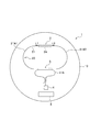
- the semiconductor ring laser device 1 includes one Si semiconductor substrate (Si wafer) 10.
- An optical waveguide 21 is formed in the Si semiconductor substrate 10, and a ring resonator 20 is configured by the optical waveguide 21.
- the ring resonator 20 has a plurality of linear optical waveguides that are folded back by a plurality of reflecting portions 22 (22A, 22B, 22C) formed in the Si semiconductor substrate 10.
- the ring resonator 20 has an annular optical waveguide including curved optical waveguides 1W1 and 21W2.
- the reflection part 22 here can be formed by forming an etching groove in the Si semiconductor substrate 10 and filling a material having a different refractive index therewith or forming a metal surface on the side surface of the groove.
- the semiconductor ring laser device 1 includes a semiconductor laser unit 2 on a Si semiconductor substrate 10.
- the semiconductor laser unit 2 may be a ring laser constituted by the light emission amplification unit 2A and the ring resonator 20 formed in at least a part of the optical waveguide 21, and etching grooves are formed at both ends of the light emission amplification unit 2A.
- a resonator may be configured by providing a transflective surface on the side surface.
- the semiconductor laser unit 2 generates two laser beams (laser beam L1 and laser beam L2) that circulate around the ring resonator 20 in opposite directions. As shown in FIG. 1, two (optical amplification units 2A1, 2A2) or three (optical amplification units 2A1, 2A2, 2A3) or more can be provided in the optical waveguide 21, as shown in FIG.
- the semiconductor ring laser device 1 includes a laser beam extraction unit 3 that extracts two laser beams L1 and L2 from the ring resonator 20.
- the laser beam extraction unit 3 uses a reflection unit 22 ⁇ / b> A provided between the optical waveguide 21 constituting the ring resonator 20 and the extraction optical waveguide 21 ⁇ / b> A as a half mirror (beam splitter).
- the optical resonator is configured by an optical directional coupler formed between the optical waveguide 21 constituting the ring resonator 20 and the extraction optical waveguide 21 ⁇ / b> A.
- the semiconductor ring laser device 1 includes a light detection unit 4 that detects a frequency difference between the two laser beams L1 and L2 extracted from the laser beam extraction unit 3.
- the light detection unit 4 is formed on the Si semiconductor substrate 10 and is integrally formed at the end of the extraction optical waveguide 21A.
- the light detection unit 4 can detect the frequency difference between the laser beams L1 and L2 by detecting the beat frequency of the laser beams L1 and L2.
- the semiconductor ring laser device 1 includes an arithmetic processing unit 5 on the Si semiconductor substrate 10 that performs arithmetic processing on a detection signal detected by the light detection unit 4.
- the arithmetic processing unit 5 may be one in which an arithmetic processing circuit is formed by a semiconductor element built in the Si semiconductor substrate 10 or an IC chip mounted on the Si semiconductor substrate 10. May be.
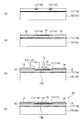
- FIG. 3 is an explanatory view showing an example of the structure and formation method of the light emission amplifying part in the semiconductor ring laser device according to the embodiment of the present invention.
- the first semiconductor layer 10 n doped with arsenic (As) is formed on the Si semiconductor substrate 10.
- the first semiconductor layer 10n is an n-type semiconductor layer.
- the SiO 2 insulating layer 11 is formed by implanting oxygen into the first semiconductor layer 10n.
- an internal insulating layer 11a is formed inside the first semiconductor layer 10n, and a pair of surface insulating layers 11b and 11c are formed on the surface of the first semiconductor layer 10n.
- the internal insulating layer 11a is formed by implanting oxygen into the surface of the Si semiconductor substrate 10 and then heat-oxidizing to diffuse the SiO 2 layer therein, or after forming the SiO 2 layer on the surface of the Si semiconductor substrate 10 It can be formed by forming a Si film.
- the pair of surface insulating layers 11b and 11c can be formed by implanting oxygen into a mask opening patterned by a photolithography process and subjecting it to a heat oxidation treatment.
- the n + layer 12 is formed by further doping arsenic (As) outside the surface insulating layers 11b and 11c, and boron (
- the second semiconductor layer (p-type semiconductor layer) 13 is formed by highly doping B).
- the metal electrode 14 is formed on the n + layer 12
- the transparent electrode (ITO or the like) 15 is formed on the second semiconductor layer 13
- the metal electrode 14 and the transparent A forward voltage is applied between the electrode 15 and boron (B) is diffused by an annealing process using Joule heat of the current flowing through the pn junction 13a.
- dressed photons are generated in the vicinity of the pn junction 13a.
- the Si semiconductor substrate itself is an indirect transition semiconductor, has low light emission efficiency, and does not provide useful light emission simply by forming a pn junction, and does not itself have light transmittance in the visible light region. .
- the Si semiconductor substrate is annealed using phonons to generate dressed photons in the vicinity of the pn junction, thereby changing Si as an indirect transition type semiconductor as if it were a direct transition type semiconductor.
- pn junction light emission with high efficiency and high output is possible.
- An example of boron (B) doping conditions for obtaining such a pn junction type light emission is a dose density of 5 ⁇ 10 13 / cm 2 , an acceleration energy at the time of implantation: 700 keV, and a wavelength of the light L irradiated in the annealing process. Is a desired wavelength band in the visible light region.
- the transparent electrode 15 is removed and the metal electrode 16 is formed on the second semiconductor layer 13, so that the light emission amplification section 2A having the pn junction 13a as the active layer. Is formed.
- the light emission amplification section 2A applies a voltage between the metal electrode 14 and the metal electrode 16 to emit light having a wavelength equivalent to the wavelength of the light L irradiated in the annealing process from the pn junction section 13a.
- FIG. 4 is an explanatory view showing an example of the structure and forming method of the optical waveguide in the semiconductor ring laser device according to the embodiment of the present invention.
- the process shown in FIG. 4A is performed in the same process as FIG. 3A described above, and an internal insulating layer 11a is formed inside the first semiconductor layer 10n, and a pair of surfaces is formed on the surface of the first semiconductor layer 10n. Surface insulating layers 11b and 11c are formed.
- the process shown in FIG. 4B is performed in the same process as the process shown in FIG. 3B.
- the n + layer 12 is omitted, and the second process is performed between the pair of surface insulating layers 11b and 11c.
- a semiconductor layer 13 is formed.
- FIG. 4C The process shown in FIG. 4C is the same as the process shown in FIG. 3C, and the metal electrode 14 is formed on the first semiconductor layer 10n outside the pair of surface insulating layers 11b and 11c. Then, after forming a transparent electrode (ITO or the like) 15 on the second semiconductor layer 13, a forward voltage is applied between the metal electrode 14 and the transparent electrode 15 to cause Joule heat of current flowing through the pn junction 13a. Boron (B) is diffused by an annealing process. Further, by irradiating the pn junction 13a with light L in the course of this annealing treatment, dressed photons are generated in the vicinity of the pn junction 13a.
- ITO transparent electrode
- the metal electrode 14 and the transparent electrode 15 are removed, whereby the optical waveguide 21 having the second semiconductor layer 13 as the light guide layer and the surface insulating layers 11b and 11c as the cladding layers. Is formed.
- the optical waveguide 21 is not limited to the forming method shown in FIGS. 4A to 4D, and for example, as shown in FIG. 4E, the first semiconductor layer in which the internal insulating layer 11a is formed. By forming the rib 10r on 10n, the rib-type optical waveguide 21 can be formed. In the example shown in FIG. 4E, the light propagating through the optical waveguide 21 is limited to infrared light that can be transmitted through the Si layer.
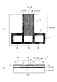
- FIG. 5 is an explanatory diagram showing an example of the structure of the light detection unit in the semiconductor ring laser device according to the embodiment of the present invention.
- the light detection unit 4 has a structure having a pn junction 13a similar to the light emission amplification unit 2A, and can be formed in the same process as the formation process shown in FIG. it can.
- the light detection unit 4 has a planar structure as shown in FIG. 5A, and is an extension of the optical waveguide 21 in which the second semiconductor layer 13 is a light guide layer and the surface insulating layers 11b and 11c are cladding layers.
- the light detection unit 4 is formed.
- the light detection unit 4 propagates through the optical waveguide 21 with zero bias or reverse bias applied between the terminals 4 a and 4 b connected to the metal electrode 14 of the light detection unit 4 and the terminal 4 c connected to the metal electrode 16. A change in generated current due to incidence of incoming laser beams L1 and L2 is output. Note that the light detection unit 4 is not limited to the example shown in FIG. 5, and can be formed by a light receiving element mounted on or connected to the Si semiconductor substrate 10.
- the operation of the semiconductor ring laser device 1 of the present invention will be described using a ring laser gyro as an example.
- the ring laser gyro detects angular velocity using the sagnac effect.
- the ring laser gyro is different in frequency between two laser beams L1 and L2 that circulate around the ring resonator 20 in opposite directions. Therefore, the rotation operation of the semiconductor ring laser device 1 can be detected by detecting the difference by the light detection unit 4.
- the laser light L1 propagating clockwise through the optical waveguide 21 forming the ring resonator 20 of the semiconductor laser section 2 is propagated counterclockwise.
- the laser beam L2 to be excited is excited.
- Part of the laser beams L1 and L2 is propagated to the extraction optical waveguide 21A via the laser beam extraction unit 3, and enters the light detection unit 4 formed at the end of the extraction optical waveguide 21A.
- the light detection unit 4 Since the laser beams L1 and L2 extracted by the extraction optical waveguide 21A are combined and enter the light detection unit 4, the light detection unit 4 detects the beat frequency of the laser beams L1 and L2, and thereby the laser beams L1 and L2 Frequency difference is detected. The angular velocity of rotation can be obtained from this frequency difference.
- the semiconductor ring laser device 1 forms the second semiconductor layer 13 by doping the first semiconductor layer 10n of the Si semiconductor substrate 10 with B (boron) at a high concentration.
- B boron
- the pn junction 13a obtained by annealing while irradiating light to the semiconductor layer 13 has a light emission amplification function, an optical waveguide function, and a light detection function on one Si semiconductor substrate 10.
- a semiconductor ring laser device 1 is formed. According to this, since the optical amplification section 2A and the light detection section 4 can be formed in a part of the optical waveguide 21, complicated optical axis alignment is not required by forming them using a series of photolithography processes.
- the arithmetic processing unit 5 that performs arithmetic processing on the detection signal of the light detection unit 4 can be integrally formed in the Si semiconductor substrate 10, it is possible to meet the demand for ultra-compact and ultra-light weight.
- 1 Semiconductor ring laser device
- 2 Semiconductor laser unit
- 2A emission amplification unit
- 3 laser beam extraction unit
- 4 light detection unit
- 5 arithmetic processing unit
- 10 Si semiconductor substrate
- 10n First semiconductor layer
- 11 Insulating layer
- 11a Internal insulating layer
- 12 n + layer
- 13 second semiconductor layer
- 13a pn junction
- 14 Metal electrode
- 15 Transparent electrode
- 20 ring resonator
- 21 optical waveguide
- 21A extraction optical waveguide
- 22 Reflection part
- L1, L2 Laser light
Landscapes
- Physics & Mathematics (AREA)
- Electromagnetism (AREA)
- Optics & Photonics (AREA)
- General Physics & Mathematics (AREA)
- Condensed Matter Physics & Semiconductors (AREA)
- Engineering & Computer Science (AREA)
- Plasma & Fusion (AREA)
- Power Engineering (AREA)
- Remote Sensing (AREA)
- Radar, Positioning & Navigation (AREA)
- Geometry (AREA)
- Semiconductor Lasers (AREA)
- Optical Integrated Circuits (AREA)
- Gyroscopes (AREA)
- Lasers (AREA)
Description
2A:発光増幅部,
3:レーザー光取り出し部,4:光検出部,5:演算処理部,
10:Si半導体基板,10n:第1半導体層,
11:絶縁層,11a:内部絶縁層,11b,11c:表面絶縁層,
12:n+層,13:第2半導体層,13a:pn接合部,
14,16:金属電極,15:透明電極,
20:リング共振器,21:光導波路,21A:取り出し光導波路,
22:反射部,L1,L2:レーザー光
Claims (6)
- 一つのSi半導体基板と、
前記Si半導体基板に形成された光導波路によって構成されるリング共振器と、
前記光導波路の少なくとも一部に発光増幅部を備え、前記リング共振器を互いに逆方向に周回する2つのレーザー光を発生させる半導体レーザー部と、
前記Si半導体基板に形成され、前記リング共振器から前記2つのレーザー光を取り出して当該2つのレーザー光の周波数差を検出する光検出部とを備え、
前記発光増幅部は、前記Si半導体基板における第1半導体層にB(ボロン)を高濃度ドープして得られる第2半導体層に光を照射しながらアニール処理を施すことで得られるpn接合部を有することを特徴とする半導体リングレーザー装置。 - 前記光検出部は、前記Si半導体基板における第1半導体層にB(ボロン)を高濃度ドープして得られる第2半導体層に光を照射しながらアニール処理を施すことで得られるpn接合部を有することを特徴とする請求項1記載の半導体リングレーザー装置。
- 前記第1半導体層は前記Si半導体基板にヒ素(As)をドープしたn型半導体層であることを特徴とする請求項1又は2に記載の半導体リングレーザー装置。
- 前記Si半導体基板は、前記光検出部の検出信号を演算処理する演算処理部を備え、
前記演算処理部は、前記Si半導体基板に作り込まれた半導体素子によって演算処理回路が形成されていることを特徴とする請求項1~3のいずれかに記載の半導体リングレーザー装置。 - 前記リング共振器は、前記Si半導体基板に形成された複数の反射部で折り返される複数の直線光導波路を有することを特徴とする請求項1~4のいずれかに記載の半導体リングレーザー装置。
- 前記リング共振器は、曲線光導波路を含む環状光導波路を有することを特徴とする請求項1~4のいずれかに記載の半導体リングレーザー装置。
Priority Applications (3)
| Application Number | Priority Date | Filing Date | Title |
|---|---|---|---|
| US14/427,532 US20150244146A1 (en) | 2012-09-14 | 2013-09-04 | Semiconductor ring laser apparatus |
| CN201380047925.5A CN104782004A (zh) | 2012-09-14 | 2013-09-04 | 半导体环形激光装置 |
| KR1020157004850A KR20150054777A (ko) | 2012-09-14 | 2013-09-04 | 반도체 링 레이저 장치 |
Applications Claiming Priority (2)
| Application Number | Priority Date | Filing Date | Title |
|---|---|---|---|
| JP2012-203152 | 2012-09-14 | ||
| JP2012203152A JP2014059170A (ja) | 2012-09-14 | 2012-09-14 | 半導体リングレーザー装置 |
Publications (1)
| Publication Number | Publication Date |
|---|---|
| WO2014042049A1 true WO2014042049A1 (ja) | 2014-03-20 |
Family
ID=50278163
Family Applications (1)
| Application Number | Title | Priority Date | Filing Date |
|---|---|---|---|
| PCT/JP2013/073778 Ceased WO2014042049A1 (ja) | 2012-09-14 | 2013-09-04 | 半導体リングレーザー装置 |
Country Status (6)
| Country | Link |
|---|---|
| US (1) | US20150244146A1 (ja) |
| JP (1) | JP2014059170A (ja) |
| KR (1) | KR20150054777A (ja) |
| CN (1) | CN104782004A (ja) |
| TW (1) | TW201415739A (ja) |
| WO (1) | WO2014042049A1 (ja) |
Cited By (1)
| Publication number | Priority date | Publication date | Assignee | Title |
|---|---|---|---|---|
| CN106996776A (zh) * | 2017-03-30 | 2017-08-01 | 中国航空工业集团公司西安飞行自动控制研究所 | 一种激光陀螺工作点恢复系统及方法 |
Families Citing this family (4)
| Publication number | Priority date | Publication date | Assignee | Title |
|---|---|---|---|---|
| JP2015210348A (ja) * | 2014-04-25 | 2015-11-24 | 株式会社日立エルジーデータストレージ | 光源モジュールおよび映像投射装置 |
| JP6278423B2 (ja) * | 2016-06-30 | 2018-02-14 | 株式会社ソディック | 発光素子 |
| CN109556591B (zh) * | 2018-11-22 | 2020-09-18 | 华中科技大学 | 一种基于超稳激光的被动式激光陀螺仪 |
| EP4096036A1 (en) * | 2021-05-26 | 2022-11-30 | EFFECT Photonics B.V. | Semiconductor ring laser, photonic integrated circuit and opto-electronic system comprising the same |
Citations (8)
| Publication number | Priority date | Publication date | Assignee | Title |
|---|---|---|---|---|
| JPH05288556A (ja) * | 1992-04-06 | 1993-11-02 | Nippon Telegr & Teleph Corp <Ntt> | 半導体レーザジャイロ |
| JP2001280973A (ja) * | 2000-03-31 | 2001-10-10 | Canon Inc | 3次元リングレーザ装置およびこれを用いたジャイロ・コンパス |
| JP2002344079A (ja) * | 2001-05-11 | 2002-11-29 | Canon Inc | 半導体リングレーザ装置及びその作製方法 |
| EP1857779A1 (en) * | 2006-05-15 | 2007-11-21 | Honeywell International Inc. | Integrated optical rotation sensor and method for sensing rotation rate |
| EP1906146A2 (en) * | 2006-09-29 | 2008-04-02 | Honeywell International Inc. | Optical resonator gyro and method for reducing resonance asymmetry errors |
| WO2009054467A1 (ja) * | 2007-10-25 | 2009-04-30 | Advanced Telecommunications Research Institute International | 半導体レーザジャイロ |
| JP2012169565A (ja) * | 2011-02-16 | 2012-09-06 | Optoelectronics Industry And Technology Development Association | 受光素子の作製方法 |
| JP2012243824A (ja) * | 2011-05-16 | 2012-12-10 | Univ Of Tokyo | 半導体レーザダイオード及びその作製方法 |
Family Cites Families (3)
| Publication number | Priority date | Publication date | Assignee | Title |
|---|---|---|---|---|
| JP2001308467A (ja) * | 2000-04-20 | 2001-11-02 | Mitsubishi Electric Corp | 光半導体装置とその製造方法 |
| JP2010164504A (ja) * | 2009-01-19 | 2010-07-29 | Rohm Co Ltd | 光ジャイロセンサ |
| JP5493430B2 (ja) * | 2009-03-31 | 2014-05-14 | ソニー株式会社 | 固体撮像装置とその製造方法、及び電子機器 |
-
2012
- 2012-09-14 JP JP2012203152A patent/JP2014059170A/ja active Pending
-
2013
- 2013-08-30 TW TW102131406A patent/TW201415739A/zh unknown
- 2013-09-04 KR KR1020157004850A patent/KR20150054777A/ko not_active Withdrawn
- 2013-09-04 CN CN201380047925.5A patent/CN104782004A/zh active Pending
- 2013-09-04 WO PCT/JP2013/073778 patent/WO2014042049A1/ja not_active Ceased
- 2013-09-04 US US14/427,532 patent/US20150244146A1/en not_active Abandoned
Patent Citations (8)
| Publication number | Priority date | Publication date | Assignee | Title |
|---|---|---|---|---|
| JPH05288556A (ja) * | 1992-04-06 | 1993-11-02 | Nippon Telegr & Teleph Corp <Ntt> | 半導体レーザジャイロ |
| JP2001280973A (ja) * | 2000-03-31 | 2001-10-10 | Canon Inc | 3次元リングレーザ装置およびこれを用いたジャイロ・コンパス |
| JP2002344079A (ja) * | 2001-05-11 | 2002-11-29 | Canon Inc | 半導体リングレーザ装置及びその作製方法 |
| EP1857779A1 (en) * | 2006-05-15 | 2007-11-21 | Honeywell International Inc. | Integrated optical rotation sensor and method for sensing rotation rate |
| EP1906146A2 (en) * | 2006-09-29 | 2008-04-02 | Honeywell International Inc. | Optical resonator gyro and method for reducing resonance asymmetry errors |
| WO2009054467A1 (ja) * | 2007-10-25 | 2009-04-30 | Advanced Telecommunications Research Institute International | 半導体レーザジャイロ |
| JP2012169565A (ja) * | 2011-02-16 | 2012-09-06 | Optoelectronics Industry And Technology Development Association | 受光素子の作製方法 |
| JP2012243824A (ja) * | 2011-05-16 | 2012-12-10 | Univ Of Tokyo | 半導体レーザダイオード及びその作製方法 |
Non-Patent Citations (5)
| Title |
|---|
| HAJIME TANAKA ET AL.: "17p-Bll-3 Homo Setsugo Si o Mochiita 1.3pm Tai no Photodiode", NEN SHUNKI (DAI 59 KAI) EXTENDED ABSTRACTS, JAPAN SOCIETY OF APPLIED PHYSICS AND RELATED SOCIETIES, 29 February 2012 (2012-02-29), pages 03-184 * |
| HAJIME TANAKA ET AL.: "Si Hikari Kenshutsuki no Kin Sekigaiiki deno Hikari Zofuku Kino Hatsugen", NEN SHUKI (DAI 73 KAI) EXTENDED ABSTRACTS; THE JAPAN SOCIETY OF APPLIED PHYSICS, 27 August 2012 (2012-08-27), pages 03-137 * |
| KAWAZOE T. ET AL.: "Si homojunction structured near-infrared laser based on a phonon-assisted process", APPLIED PHYSICS B, vol. 107, 25 May 2012 (2012-05-25), pages 659 - 663 * |
| TADASHI KAWAZOE ET AL.: "17p-Bll-6 Homo Setsugo Si o Mochiita Si Laser no Dosa Kensho", NEN SHUNKI (DAI 59 KAI) EXTENDED ABSTRACTS, JAPAN SOCIETY OF APPLIED PHYSICS AND RELATED SOCIETIES, 29 February 2012 (2012-02-29), pages 03-187 * |
| TANAKA H. ET AL.: "Increasing Si photodetector photosensitivity in near-infrared region and manifestation of optical amplification by dressed photons", APPLIED PHYSICS B, vol. 108, 24 May 2012 (2012-05-24), pages 51 - 56 * |
Cited By (2)
| Publication number | Priority date | Publication date | Assignee | Title |
|---|---|---|---|---|
| CN106996776A (zh) * | 2017-03-30 | 2017-08-01 | 中国航空工业集团公司西安飞行自动控制研究所 | 一种激光陀螺工作点恢复系统及方法 |
| CN106996776B (zh) * | 2017-03-30 | 2020-04-07 | 中国航空工业集团公司西安飞行自动控制研究所 | 一种激光陀螺工作点恢复系统及方法 |
Also Published As
| Publication number | Publication date |
|---|---|
| US20150244146A1 (en) | 2015-08-27 |
| CN104782004A (zh) | 2015-07-15 |
| JP2014059170A (ja) | 2014-04-03 |
| KR20150054777A (ko) | 2015-05-20 |
| TW201415739A (zh) | 2014-04-16 |
Similar Documents
| Publication | Publication Date | Title |
|---|---|---|
| CN114830464B (zh) | 具有增益调节用于提高性能的基于环形波导的集成光子光学陀螺仪 | |
| Liu et al. | Optical amplification and lasing by stimulated Raman scattering in silicon waveguides | |
| US10027089B2 (en) | Coupled ring resonator system | |
| US7564563B2 (en) | Laser gyro and electronic device using the same | |
| Bonneville et al. | High on-chip gain spiral Al2O3: Er3+ waveguide amplifiers | |
| EP1393017B1 (fr) | Gyrometre laser etat solide comportant un bloc resonateur | |
| JPH07117620B2 (ja) | 光 源 | |
| JP2014059170A (ja) | 半導体リングレーザー装置 | |
| CN107809058B (zh) | 一种单片集成半导体随机激光器 | |
| US11431153B2 (en) | Semiconductor optical amplifier, light output apparatus, and distance measuring apparatus | |
| CN104993374B (zh) | 一种单模激射圆环微腔激光器 | |
| US9562768B2 (en) | Active waveguide optical gyroscope | |
| JP4728989B2 (ja) | ラマン散乱光増強デバイス | |
| CN100561127C (zh) | 使用半导体激光器的陀螺仪 | |
| JP2007013065A (ja) | 近赤外光検出素子 | |
| JP5338796B2 (ja) | 光ジャイロ | |
| CN105470792A (zh) | 高功率两芯共腔光纤激光器 | |
| Rong et al. | Monolithic integrated ring resonator Raman silicon laser and amplifier | |
| JP2008002954A (ja) | 光ジャイロ | |
| Koyama | High Power VCSEL Amplifier for 3D Sensing | |
| CN119764984A (zh) | 一种集成于薄膜铌酸锂片上的ase光源结构 | |
| Gu et al. | Fractal superconducting nanowire single-photon detectors with low polarization sensitivity | |
| WO2006103850A1 (ja) | 導波路素子及びレーザ発生器 | |
| Lim et al. | Introduction to Lidar | |
| KR20250046603A (ko) | 연속 주파수 가변 어레이 광원 |
Legal Events
| Date | Code | Title | Description |
|---|---|---|---|
| 121 | Ep: the epo has been informed by wipo that ep was designated in this application |
Ref document number: 13837352 Country of ref document: EP Kind code of ref document: A1 |
|
| ENP | Entry into the national phase |
Ref document number: 20157004850 Country of ref document: KR Kind code of ref document: A |
|
| WWE | Wipo information: entry into national phase |
Ref document number: 14427532 Country of ref document: US |
|
| NENP | Non-entry into the national phase |
Ref country code: DE |
|
| 122 | Ep: pct application non-entry in european phase |
Ref document number: 13837352 Country of ref document: EP Kind code of ref document: A1 |