WO2014034833A1 - 保護素子 - Google Patents
保護素子 Download PDFInfo
- Publication number
- WO2014034833A1 WO2014034833A1 PCT/JP2013/073264 JP2013073264W WO2014034833A1 WO 2014034833 A1 WO2014034833 A1 WO 2014034833A1 JP 2013073264 W JP2013073264 W JP 2013073264W WO 2014034833 A1 WO2014034833 A1 WO 2014034833A1
- Authority
- WO
- WIPO (PCT)
- Prior art keywords
- metal
- layer
- opening
- melting point
- protective element
- Prior art date
- Legal status (The legal status is an assumption and is not a legal conclusion. Google has not performed a legal analysis and makes no representation as to the accuracy of the status listed.)
- Ceased
Links
Images



Classifications
-
- H—ELECTRICITY
- H01—ELECTRIC ELEMENTS
- H01H—ELECTRIC SWITCHES; RELAYS; SELECTORS; EMERGENCY PROTECTIVE DEVICES
- H01H85/00—Protective devices in which the current flows through a part of fusible material and this current is interrupted by displacement of the fusible material when this current becomes excessive
- H01H85/02—Details
- H01H85/04—Fuses, i.e. expendable parts of the protective device, e.g. cartridges
- H01H85/05—Component parts thereof
- H01H85/055—Fusible members
- H01H85/08—Fusible members characterised by the shape or form of the fusible member
- H01H85/11—Fusible members characterised by the shape or form of the fusible member with applied local area of a metal which, on melting, forms a eutectic with the main material of the fusible member, i.e. M-effect devices
-
- H—ELECTRICITY
- H01—ELECTRIC ELEMENTS
- H01M—PROCESSES OR MEANS, e.g. BATTERIES, FOR THE DIRECT CONVERSION OF CHEMICAL ENERGY INTO ELECTRICAL ENERGY
- H01M50/00—Constructional details or processes of manufacture of the non-active parts of electrochemical cells other than fuel cells, e.g. hybrid cells
- H01M50/50—Current conducting connections for cells or batteries
- H01M50/572—Means for preventing undesired use or discharge
- H01M50/574—Devices or arrangements for the interruption of current
- H01M50/583—Devices or arrangements for the interruption of current in response to current, e.g. fuses
-
- H—ELECTRICITY
- H02—GENERATION; CONVERSION OR DISTRIBUTION OF ELECTRIC POWER
- H02H—EMERGENCY PROTECTIVE CIRCUIT ARRANGEMENTS
- H02H3/00—Emergency protective circuit arrangements for automatic disconnection directly responsive to an undesired change from normal electric working condition with or without subsequent reconnection ; integrated protection
- H02H3/08—Emergency protective circuit arrangements for automatic disconnection directly responsive to an undesired change from normal electric working condition with or without subsequent reconnection ; integrated protection responsive to excess current
- H02H3/085—Emergency protective circuit arrangements for automatic disconnection directly responsive to an undesired change from normal electric working condition with or without subsequent reconnection ; integrated protection responsive to excess current making use of a thermal sensor, e.g. thermistor, heated by the excess current
-
- Y—GENERAL TAGGING OF NEW TECHNOLOGICAL DEVELOPMENTS; GENERAL TAGGING OF CROSS-SECTIONAL TECHNOLOGIES SPANNING OVER SEVERAL SECTIONS OF THE IPC; TECHNICAL SUBJECTS COVERED BY FORMER USPC CROSS-REFERENCE ART COLLECTIONS [XRACs] AND DIGESTS
- Y02—TECHNOLOGIES OR APPLICATIONS FOR MITIGATION OR ADAPTATION AGAINST CLIMATE CHANGE
- Y02E—REDUCTION OF GREENHOUSE GAS [GHG] EMISSIONS, RELATED TO ENERGY GENERATION, TRANSMISSION OR DISTRIBUTION
- Y02E60/00—Enabling technologies; Technologies with a potential or indirect contribution to GHG emissions mitigation
- Y02E60/10—Energy storage using batteries
Definitions
- the present invention relates to a protective element for protecting an electric device, and more particularly to a protective element for protecting an electric element or circuit included in the electric device.
- the present invention relates to a protection element that cuts off a current flow when an excessive current flows in an electric device such as a secondary battery, that is, an overcurrent protection element.
- a thermal fuse element, a current fuse element, a polymer PTC element, or the like is used as a protective element that cuts off the current flow when an excess current flows during charging or discharging of a cylindrical lithium ion secondary battery.
- the polymer PTC element can be arranged by being incorporated in a sealing plate of a secondary battery, it is particularly useful in that a battery pack constituted by a large number of secondary batteries becomes compact.
- a commercially available annular PTC element cannot continuously carry a large current (for example, a current of 10 A).
- the PTC element has a recoverability that becomes low resistance when the abnormality is removed and the temperature is lowered, but there may be a problem depending on the application.
- the cell continues to generate heat unless the short-circuited cell using the PTC element is removed, resulting in a battery cell. May burst.
- Non-Patent Document 1 it has been proposed to use a spacer instead of the PTC element inside the sealing plate, for example, in the cylindrical lithium ion secondary battery cell (see Non-Patent Document 1 below). .
- a spacer when a spacer is used, there is a problem that protection against excess current cannot be secured.
- the overcurrent protection element it is preferable to quickly and surely cut off the excess current even if it is an excess current that does not greatly exceed the rated capacity, for example, an excess current that is about twice the rated capacity. Therefore, the problem to be solved by the present invention is to ensure that even when an excessive current that does not greatly exceed the rated capacity, for example, an excess current that is about twice the rated capacity, can be passed while allowing a larger current to flow. It is to provide a protective element that can provide quick protection.
- the present invention provides: A layered element formed of insulating resin and having at least one through opening; A conductive metal thin layer located on each main surface of the layered element, and a fuse layer located on a side surface defining at least one of the through openings and electrically connecting the conductive metal thin layer; A protective element comprising a fuse layer including at least a first metal layer made of a high melting point metal and a second metal layer made of a low melting point metal is provided.
- the present invention provides an electric device, for example, a secondary battery, comprising the protective element of the present invention as described above and below.
- the protective element of the present invention comprises a layered element formed of an insulating resin, and this layered element has at least one through opening.
- the opening extends along the thickness direction of the layered element and penetrates the layered element, and the cross-sectional shape in the direction perpendicular to the thickness direction is not particularly limited, but is circular, for example. Is preferred. However, other shapes, such as squares, rhombuses, rectangles, and ellipses may be used.
- the number of through openings is at least one. That is, it may be one or two or more, for example, two, three, four, five, eight, or nine, but is appropriately selected depending on the degree of protection required for the protective element. it can. In the case of having one through opening, the through opening is preferably located at the center of the layered element, that is, the center of the cross-sectional shape in the direction perpendicular to the thickness direction.
- the insulating resin constituting the layered element is not particularly limited as long as it is an electrically insulating resin.
- resins such as polyethylene, polypropylene, polycarbonate, fluorine resin, ABS resin, polycarbonate-ABS alloy resin, PBT resin, and elastomer.
- a resin such as polyethylene or polyvinylidene fluoride.
- Such a resin has the same flexibility as the polymer used for the polymer PTC element, and the protective element of the present invention is used instead of the polymer PTC element.
- the protective element of the present invention can be used in place of the spacer used inside the sealing plate of the secondary battery cell described above, in which case the protective element is used as a washer. be able to.
- the layered element comprises a thin conductive metal layer disposed on the main surface on both sides thereof.
- the conductive metal thin layer is not particularly limited as long as it is a thin layer of conductive metal (for example, a thickness of about 0.1 ⁇ m to 100 ⁇ m).
- conductive metal for example, copper, nickel, aluminum, gold, etc. It can be composed of metal and may be formed of a plurality of thin metal layers.
- a layered element in which a thin conductive metal layer is located on each main surface is obtained by simultaneously extruding an insulating resin constituting the layered element together with a metal sheet (or metal foil) constituting the thin metal layer. It can be manufactured by obtaining an extrudate in which an insulating resin is sandwiched between sheets (or metal foils).
- a layered product of an insulating resin is obtained by, for example, extrusion, the layered product is sandwiched between metal sheets (or metal foils), and these are thermocompression bonded together to obtain a pressed product. You can also.
- Such an extrudate is a state in which a large number of layered elements of insulating resin having conductive metal thin layers on both main surfaces are gathered adjacent to each other.
- a layered element having a single conductive thin layer can be obtained by cutting into a predetermined shape and size.
- a conductive metal thin layer may be formed on the main surfaces on both sides by plating a conductive metal on the insulating resin layered element. In this case as well, it is preferable to obtain the aggregated state as described above and then divide it into individual layered elements.
- the layered element is preliminarily separated from the layered element by extruding or thermocompressing another metal layer, particularly preferably a metal foil, on its main surface, for example as described above. It is particularly preferable to keep it in close contact. In this case, it is preferable to form a thin conductive metal layer by plating on the other metal layer.
- this conductive metal thin layer is formed by plating, it is advantageous in that the plating layer as the conductive metal thin layer can be in close contact with another metal layer in close contact with the layered element.
- the protective element of the present invention has a conductive metal thin layer and a fuse layer formed by nickel plating and tin plating having nickel foil or nickel plated copper foil as another metal layer on both main surfaces of the layered element. It has a metal layer to constitute.
- the form of the layered element is not particularly limited as long as the dimension in the thickness direction is smaller than the other dimensions, and preferably considerably small (for example, a sheet-like form).
- the plane shape of the layered element (the figure when the layered element is viewed from directly above, for example, the contour shape of the protective element shown in FIG. 2) or the cross-sectional shape in the direction perpendicular to the thickness direction of the layered element is geometrically linear. It is preferable to have a main surface having a symmetrical and / or point-symmetrical shape, for example, a circular shape, a square shape, a rectangular shape, a diamond shape, an annular shape (particularly an annular shape, a so-called donut shape).
- the layered element is preferably annular, particularly annular.
- the central opening for example, the central circular opening in the case of an annular shape, may be the through opening of the present invention.
- the layered element has one or more additional through openings, for example, through holes having a circular cross section, at a portion between the inner circumference and the outer circumference defining the ring shape (for example, an intermediate portion thereof). It's okay.
- the protection element of the present invention has a fuse layer that is located on a side surface that defines at least one of such through-openings and that electrically connects thin conductive metal layers located on both main surfaces of the layered element.
- the fuse layer includes at least two types of metal layers having different melting points (hereinafter, of the two types of metal layers, a layer made of a refractory metal is referred to as a “first metal layer” and a layer made of a low melting point metal. (Referred to as “second metal layer”).
- the fuse layer may be composed of three or more metal layers. When the fuse layer is composed of three or more metal layers, the metals forming these layers do not have to be different from each other, and at least two types may be different.
- the melting point of another metal layer other than the first metal layer and the second metal layer is a temperature not lower than the melting point of the second metal layer, more preferably not higher than the melting point of the first metal layer, and the second metal layer.
- the temperature is higher than the melting point of.
- the stacking order is not limited and can be set as appropriate according to product requirements.
- the metal forming the outermost layer can be Ni or the like.
- the metal layer is preferably laminated, but is not limited to this. For example, one layer is formed around the half of the through opening, and another layer is formed around the other half. May be formed.
- the protective element of the present invention can be used even when an excess current of 1.2 to 4 times, preferably 1.5 to 2.0 times the rated capacity of the protective element flows.
- the generation of arc can be suppressed, and excess current can be cut off quickly and reliably.
- the protection element of the present invention blocks excess current as follows.
- excessive current flowing from the thin conductive metal layer on one main surface to the thin conductive metal layer on the other main surface excessive current flows through the fuse layer and generates heat.
- the second metal layer made of a low melting point metal is melted.
- the current flowing in the second metal layer also flows in the first metal layer, and the current flowing in the first metal layer increases. Therefore, an excess current at a low magnification of the rated capacity of the protective element, for example, 1. Even when an excess current of 5 to 2.0 times flows, the first metal layer is quickly melted, and the excess current is quickly and reliably interrupted.
- the metal layer having the lowest melting point is first melted and current is commutated to the remaining metal layers, and the current flowing through these metal layers is the same as above. Will increase. And by repeating such fusing and commutation sequentially, the fuse layer is blown quickly, and the excess current is cut off quickly and reliably.
- the metal forming the metal layer is not particularly limited as long as it is conductive.
- Ni-B alloy Ni, Ni, Cu, Ag, Au, Al, Zn, Rh, Ru, Ir, Pd, Pt, Ni—P Alloy, Ni-B alloy, Sn, Sn-Ag alloy, Sn-Cu alloy, Sn-Ag-Cu alloy, Sn-Ag-Cu-Bi alloy, Sn-Ag-Cu-Bi-In alloy, Sn-Ag- Bi—In alloy, Sn—Ag—Cu—Sb alloy, Sn—Sb alloy, Sn—Cu—Ni—P—Ge alloy, Sn—Cu—Ni alloy, Sn—Ag—Ni—Co alloy, Sn—Ag— Cu—Co—Ni alloy, Su—Bi—Ag alloy, Sn—Zn alloy, Sn—In alloy, Sn—Cu—Sb alloy, Sn—Fe alloy, Zn—Ni alloy, Zn—Fe alloy, Zn—Co alloy ,
- the refractory metal is not limited, but, for example, Ni, Cu, Ag, Au, Al, Zn, Sn, Rh, Ru, Ir, Pd, Pt, Sn, Ni—Au alloy, Ni-P alloy and Ni-B alloy are mentioned.
- the first metal layer is preferably formed by electroless plating of the refractory metal, but is not limited thereto.
- low melting point metal examples include, but are not limited to, Sn, Sn—Ag alloy, Sn—Cu alloy, Sn—Ag—Cu alloy, Sn—Ag—Cu—Bi alloy, Sn—Ag—Cu—.
- the low melting point metal is preferably a conductive metal having a melting point lower than the decomposition temperature of the insulating resin constituting the layered element.
- a conductive metal having a melting point lower than the decomposition temperature of the insulating resin constituting the layered element when an excess current flows, the fuse layer is cut before the decomposition temperature of the insulating resin is reached, and the insulation Decomposition of the functional resin can be prevented.
- the decomposition temperature of the insulating resin refers to a temperature at which the insulating resin is thermally decomposed, and can be measured by, for example, a differential thermothermal weight simultaneous measurement apparatus (TG-DTA).
- the insulating resin is high-density polyethylene
- a gradual weight loss is observed between 300 and 550 ° C. in air, and a rapid weight loss occurs particularly at 400 ° C. or higher. That is, 400 ° C. is the decomposition temperature.
- the second metal layer is preferably formed by electroplating the low melting point metal on the first metal layer, but is not limited thereto.
- the thickness of the fuse layer is not particularly limited, but is preferably 0.001 to 0.02 mm, and more preferably 0.002 to 0.015 mm.
- the thickness of the fuse layer is less than 0.001 mm, it is difficult to form a uniform plating layer, and pinholes or the like may occur.
- the thickness of the fuse layer exceeds 0.02 mm, the time and cost for plating are increased. In such a case, it is preferable to adjust the element characteristics by increasing the number of through openings or the diameter of the through openings.
- the thickness ratio of each metal layer in the fuse layer is not particularly limited as long as desired characteristics can be obtained.
- the fuse layer includes the first metal layer and the second metal layer
- the first metal The ratio of the layer to the second metal layer (thickness ratio) is 1: 100 to 5: 1, preferably 1:25 to 3: 5, more preferably 1:25 to 3:10.
- the layered element When a single through opening having a fuse layer on the side is provided, the layered element is circular or other suitable flat plate shape without holes, and its central portion (planar shape is circular (ie, disk shape) It is preferable to provide a through opening (also referred to as “center through opening”) in such a layered element where such a central portion exists). As a result, the layered element has a strictly annular shape. The current flowing through the thin conductive metal layer on one main surface of the layered element having such an annular shape flows toward one end of the through opening, and then passes through the fuse layer to form the through opening. Flows radially from the other end of the part over the thin conductive metal layer on the other main surface of the layered element.
- a larger through opening is formed in the central part of the annular element as compared with an aspect in which a plurality of through openings to be described in detail later is provided.
- the opening is preferably provided, and a fuse layer is provided on the side surface of the through opening. Since such a protective element can reduce the resistance value, a large current (preferably a current larger than 20 A, such as a current of 30 to 40 A or larger, such as 50 A) is selected by selecting a suitable metal layer material. It can be suitably used when flowing. Moreover, since only one through opening is provided, the manufacture of the protective element is simplified.
- the layered element has an annular shape defined by an inner periphery 30 and an outer periphery 34 as shown in FIG. 2 or FIG.
- the diameter of the circle defining the inner circumference of the layered element is preferably 6 to 16 mm, for example, and the diameter of the circle defining the outer circumference is preferably 13 to 24 mm, for example.
- the diameter of a circle on the inner circumference is, for example, 6.5 mm, and the thickness of the fuse layer is, for example, 0.008 mm.
- a through opening having the same cross-sectional shape and size (“In this case, it is preferable to provide the through openings at an equal angle with respect to the center of the inner circumferential circle that defines the ring. For example, two through openings are provided every 180 °, three every 120 °, four every 90 °, and six every 60 °.
- the layered element may have only one peripheral through opening. Therefore, the number of circumferential through openings may be 1 to 6, for example.
- a fuse layer may also be provided on the side surface defining such a central through opening.
- the diameter of the cross-sectional circle of the central through opening is larger than the diameter of the cross-sectional circle of the peripheral through opening, it is preferable not to provide a fuse layer in the central through opening.
- Whether or not the fuse layer is provided in the central through opening as described above is determined by whether or not the current flowing through the fuse layer provided in each through opening of the protective element is substantially equal.
- the central through opening has a larger circular cross section than the peripheral through opening, if a fuse layer is provided in the central through opening, substantially the majority of the current flowing through the protective element is likely to flow through the fuse layer, Since it is difficult for current to flow through the fuse layer provided in another through opening having a smaller circular cross section, the meaning of providing the fuse layer in the other through opening is reduced.
- the layered element is an annular element defined by an outer circumference and an inner circumference, a through opening is defined by the inner circumferential surface, and another through opening is located inside the layered element, ie Further, it may be provided as a peripheral through-opening through between the inner periphery and the outer periphery that define the layered element (that is, the portion of the insulating resin that defines the layered element). Accordingly, in this case, the layered element has a central through opening (one) defined by the inner circumference and at least one through opening (corresponding to the peripheral through opening described above) penetrating through the body part of the layered element.
- the fuse layer exists on the side surface (that is, the wall) that defines the peripheral through opening. If the diameter of the central through-opening is not much different from the diameter of the peripheral through-opening and a fuse layer exists in the central through-opening, current flows through the fuse layer in the same way as the fuse layer of the peripheral through-opening. If expected, a fuse layer may also be provided in the central through opening. When the diameter of the central through opening is larger than the diameter of the peripheral through opening and a fuse layer exists in the central through opening, a much larger amount of current flows through the fuse layer than the fuse layer of the peripheral through opening. In the case where it is expected, there is no point in providing a fuse layer in the peripheral through opening, and therefore no fuse is provided in the central through opening.
- the central through opening does not have a fuse layer and is arranged circumferentially around it. And a plurality of peripheral through openings.
- the circumference in which the peripheral through-opening is provided is usually preferably single, but in some cases, it may be a multiple circumference, for example, a double circumference or a triple circumference.
- the resistance value of the protection element can be controlled according to the number of peripheral through openings provided. Accordingly, there is an advantage that the resistance value of the protection element can be easily and precisely changed by simply changing the number of through openings provided, as compared with the above-described embodiment in which the fuse layer is provided only in the central through opening.
- the peripheral through-opening is preferably located in contrast to the center of the layered element when the layered element is ring-shaped, for example annular.
- the center of the annular element that is, the figure defining the inner circumference, for example, the same angle around the center of the circle, for example, two every 180 °, three every 120 ° , Preferably there are four every 90 °.
- the diameter of the central through opening (without the fuse layer) is 6 to 16 mm, and the diameter of the sectional circle around the peripheral through opening (with the fuse layer) is 0.2 to 1 mm.
- the outer diameter of the layered element is preferably 13 to 24 mm, for example.
- eight peripheral through openings having a diameter of 0.6 mm are provided, and the thickness of the fuse layer is preferably 0.008 mm, for example.
- the through opening may have any other suitable cross-sectional shape, and preferably has a circular cross section.
- a square, a rectangle, a rhombus, a triangle, etc. may be sufficient.
- the above-mentioned diameter corresponds to the equivalent diameter of another cross-sectional shape.
- the cross-sectional shape of the through-opening the size (usually the diameter) of the through-opening and the length in the thickness direction, the thickness of the fuse layer, the fuse so as to melt in accordance with the assumed excess current amount
- Various factors such as the material of each metal layer and the ratio of each metal layer in the layer, and the number and arrangement of the through openings are selected, and the numerical values are selected in a predetermined manner. This selection can be made by those skilled in the art with respect to these factors, for example by trial and error.
- the thin conductive metal layer and the fuse layer are integrally formed by high-melting point metal plating and low-melting point metal plating, more preferably by Ni plating and Sn plating.
- the fuse layer includes a first metal layer (Ni plating) and a second metal layer (Sn plating).
- Ni plating Ni plating
- Sn plating second metal layer
- the conductive metal thin layer and the fuse layer can be formed simultaneously and integrally by plating the layered element having the through opening with the high melting point metal and the low melting point metal. That is, the fuse layer and the conductive metal thin layer are formed of the same type of metal.
- an electrolytic plating method or an electroless plating method can be used, but an electroless plating method is used for a high melting point metal and an electrolytic plating method is used for a low melting point metal. It is preferable.
- a metal foil preferably nickel foil or nickel-plated copper foil, which is in close contact with the layered element, between the layered element and the conductive metal thin layer.
- the conductive metal thin layer formed as the plating layer can be in close contact with the metal foil, and as a result, the conductive metal thin layer is firmly bonded to the layered element via the metal foil.
- the protection element of the present invention includes a first electric element (for example, a secondary battery) and a second electric element (for example, a charger) as another electric element in order to protect a circuit to be protected or an electric element constituting the circuit. Between the two, so that one of the thin conductive metal layers is in direct or indirect contact with the first electrical element and the other conductive The thin metal layer is in direct or indirect contact with the second electrical element. Accordingly, the present invention also provides an electrical device comprising the protection element of the present invention and the circuits and / or electrical elements electrically connected thereby.
- a first electric element for example, a secondary battery
- a second electric element for example, a charger
- the protection element of the present invention has a thin conductive metal layer on the main surfaces on both sides of the layered element, and allows a large current to flow by electrically connecting them with the fuse layer, but also an excess current.
- the current flows, the current flows intensively in the fuse layer. As a result, the fuse layer melts and the circuit is cut off, whereby the current flow can be cut off.
- FIG. 1 schematically shows a protection element of the present invention in a sectional view along the thickness direction.
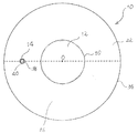
- FIG. 2 schematically shows the protection element shown in FIG. 1 in a plan view.
- FIG. 3 schematically shows a fuse layer in the protection element shown in FIGS. 1 and 2 in a sectional view.
- FIG. 4 schematically shows a protective element according to another aspect of the present invention in a cross-sectional view along the thickness direction.
- FIG. 5 schematically shows the protection element shown in FIG. 4 in a plan view.
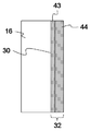
- FIG. 6 schematically shows the fuse layer in the protection element shown in FIGS. 4 and 5 in a cross-sectional view.
- FIG. 1 schematically shows one embodiment of the protection element of the present invention in a cross-sectional view along the thickness direction (a portion appearing as a cut surface is indicated by A), and FIG. Is schematically shown in a plan view. Further, FIG. 3 schematically shows a fuse layer of the protection element shown in FIGS. 1 and 2 in a sectional view.
- the illustrated protection element 10 is formed of an insulating resin, and includes at least one through opening, in the illustrated embodiment, two through openings, a central through opening 12 having a circular cross section and a peripheral through opening 14 having a circular cross section. And having an annular layered element 16. It has thin conductive metal layers 22 and 24 located on the major surfaces 18 and 20 on both sides of the layered element 16. In the illustrated embodiment, there are additional metal layers 26 and 28 between the layered element 16 and the thin conductive metal layer.
- a fuse layer 40 is present on a circumferential side 38 that defines a peripheral through opening 14 located in the body portion 36 of the layered element between the inner periphery 30 and the outer periphery 34 of the annulus.
- the fuse layer 40 includes a first metal layer 41 that exists on the circumferential side surface 38 that defines the peripheral through-opening 14, and a second metal layer 42 that exists on the first metal layer 41.
- peripheral through opening 14 having a fuse layer 40 is provided in the middle of the body portion 36 along a diameter (shown in broken lines in FIG. 2) that passes through the center O of the layered element.
- a peripheral through opening may be provided on the opposite side along the diametrical direction. In that case, a peripheral through opening is provided around the center O every 180 °.
- a perforation that has three fuse layers, eg, every 120 °, four every 90 °, six every 60 °, or eight every 45 °, with respect to the center O of the circle. The openings may be provided at an equal angle.
- the protective element can be positioned on the electric device.
- the protective element can be positioned on the sealing plate by providing such a convex portion on the sealing plate of the secondary battery cell and fitting the convex portion into the central through opening.
- the layered element 16 does not have a central through-opening 12 (and thus the layered element is disk-shaped) and has only at least one peripheral through-opening 14 that has a fuse layer 40. You can do it.
- FIGS. 4 and 5 A protective element 10 'according to still another embodiment of the present invention is shown in FIGS. 4 and 5 in the same manner as FIGS.
- the fuse layer 32 is shown in FIG. 6 as in FIG.
- the same reference numerals are used for the same elements as in FIGS.
- the layered element 16 does not have the peripheral through opening 14 but only the central through opening 12, which has the fuse layer 32.
- the fuse layer 32 includes a first metal layer 43 that exists on the inner periphery 30 that defines the central through opening 12, and a second metal layer 44 that exists on the first metal layer 43.
- Example 1 The protection element of the present invention shown in FIGS. 1 and 2 was manufactured. Therefore, the protection element 10 having only the fuse layer 40 and not having the fuse layer 32 was manufactured. However, eight peripheral through openings 14 were formed at equal intervals in the circumferential shape.
- a sheet of insulating resin (made of polyethylene, thickness 0.3 mm, corresponding to the layered element 16) is prepared, and nickel foil (thickness: 22 ⁇ m, corresponding to the other metal layers 26 and 28) is provided on both sides thereof. These were placed and pressed together under heating to obtain a press-bonded product in which nickel foil was attached to both main surfaces.
- a through hole having a diameter of 0.6 mm (corresponding to the peripheral through opening 14) was formed at a predetermined location of the pressure-bonded product, and then the pressure-bonded material was subjected to Ni plating by an electroless method.
- the thickness of the nickel layer formed by the Ni plating process was about 1.5 ⁇ m.
- the pressure-bonded product was subjected to Sn plating by an electrolytic method.
- the thickness of the tin layer formed by the Sn plating process was about 6.5 ⁇ m.
- a conductive metal thin layer (corresponding to the conductive metal thin layers 22 and 24), a first metal layer (corresponding to the first metal layer 41), and a second metal layer (corresponding to the second metal layer 42).
- a fuse layer (corresponding to the fuse layer 40) was obtained.
- the annular element was punched out from the pressure-bonded article, and the protective element 10 of the present invention was obtained in which the eight through holes are positioned at predetermined positions around the center of the annular element at every 45 °.
- the diameter of the outer peripheral circle 34 of the obtained annular element was 15 mm, and the diameter of the inner periphery 30 (that is, the diameter of the central through opening) was 6.4 mm.
- This annular element has nickel foils functioning as separate metal layers 26 and 28 on both main surfaces of the insulating resin layer as the layered element 16, and a peripheral through opening at an intermediate part of the main body part 36 of the annular part. 14 Further, the annular element has plating layers (nickel plating layer and tin plating layer) as the conductive metal thin layers 22 and 24 on the nickel foil, and the first metal is formed on the inner peripheral surface defining the peripheral through opening. A plating layer functioning as the fuse layer 40 composed of the layer 41 and the second metal layer 42 was provided.
- Example 2 to Example 2 were carried out in the same manner as Example 1 except that Sn—Cu (Cu 4 wt%) plating treatment and Sn—Bi (Bi 16 wt%) plating treatment were carried out instead of tin plating treatment, respectively. 4 protective elements were obtained.
- Comparative Examples 1 to 3 Example except that nickel plating is performed instead of tin plating, and the thickness of the nickel plating layer formed by the nickel plating is 4.5, 6.5, and 8.5 ⁇ m, respectively. In the same manner as in Example 1, protective elements of Comparative Examples 1 to 3 were obtained.
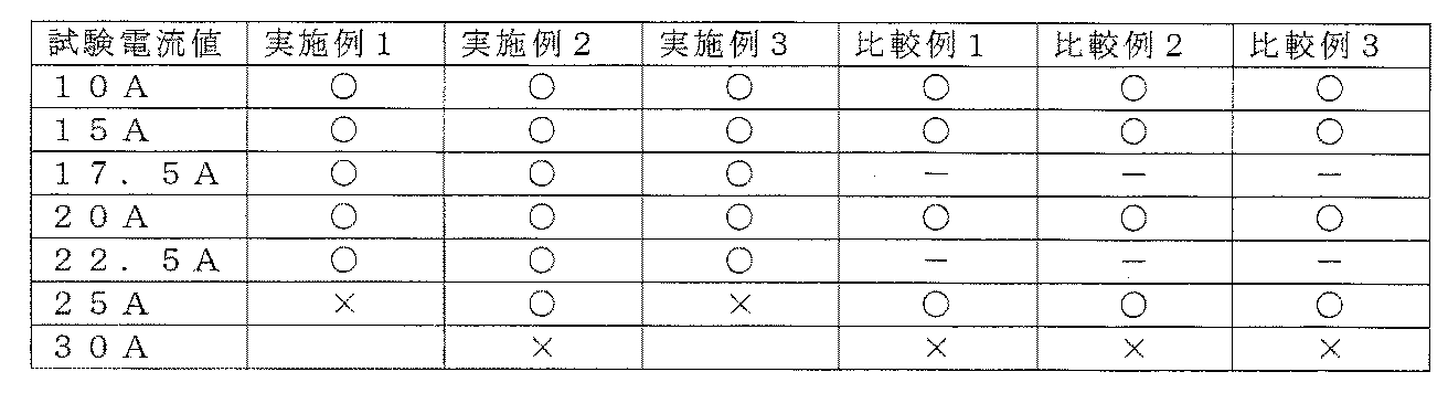
- Test Example 1 When the current shown in Table 2 below was passed through the protective elements of Examples 1 to 3 and Comparative Examples 1 to 3 from one conductive metal thin layer 22 to the other conductive metal thin layer 24, and energized for 10 minutes.
- the current value at which the fuse layer did not blow was investigated (60 Vdc setting). In each case, the maximum current value at which the fuse layer did not blow (blow) was defined as the rated capacity.
- the results are shown in Table 2. In the table, “ ⁇ ” indicates that blowing was not performed for 10 minutes, “ ⁇ ” indicates that blowing was performed within 10 minutes, and “ ⁇ ” indicates that there was no data.
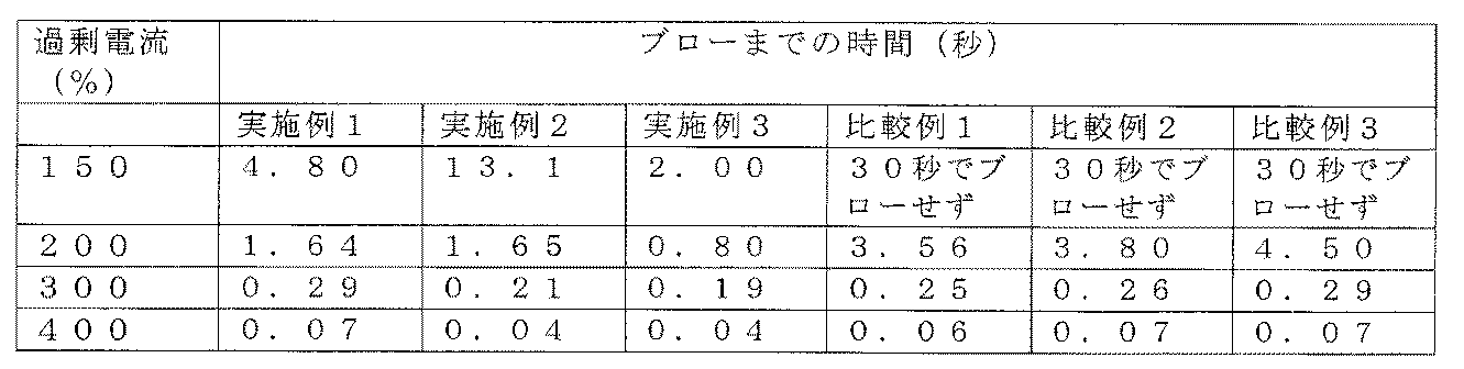
- Test Example 2 In the protective elements of Examples 1 to 3 and Comparative Examples 1 to 3, from one conductive metal thin layer 22 to the other conductive metal thin layer 24, 150%, 200%, 300%, and An excess current of 400% was applied, and the current interruption time (that is, the time until the fuse layer was blown) was measured. The results are shown in Table 3 below.
- the protective element of the present invention can be used as a protective element that cuts off the current flow when an excessive current flows in an electric device such as a secondary battery.
- the protective element of the present invention can also be used as a substitute for, for example, a nickel washer incorporated in a sealing plate or a washer obtained by applying nickel plating to a stainless material in a cylindrical lithium ion secondary battery cell.
- the protective element since the protective element has a layered element formed of an insulating resin, the function as a washer is improved by the elasticity of the resin. Therefore, the protection element of the present invention can be used as a washer having the characteristics of the protection element of the present invention described above.
Landscapes
- Chemical & Material Sciences (AREA)
- Chemical Kinetics & Catalysis (AREA)
- Electrochemistry (AREA)
- General Chemical & Material Sciences (AREA)
- Fuses (AREA)
Description
そこで、本発明が解決しようとする課題は、より大きい電流を流すことを可能にしながら、定格容量をそれほど大きく上回らない過剰電流、例えば定格容量の2倍程度の過剰電流に対しても、確実かつ迅速な保護を提供できる保護素子を提供することである。
絶縁性樹脂により形成され、少なくとも1つの貫通開口部を有する層状要素、
層状要素の各主表面上に位置する導電性金属薄層、および
該貫通開口部の少なくとも1つを規定する側面上に位置し、導電性金属薄層を電気的に接続するヒューズ層であって、少なくとも、高融点金属からなる第1金属層および低融点金属からなる第2金属層を含むヒューズ層
を有して成る、保護素子を提供する。
図1および図2に示す本発明の保護素子を製造した。従って、ヒューズ層40のみを有し、ヒューズ層32を有さない保護素子10を製造した。但し、周辺貫通開口部14は、周状に等間隔で8つ形成した。
スズメッキ処理に代えて、それぞれ、Sn-Cu(Cu 4重量%)メッキ処理、およびSn-Bi(Bi 16重量%)メッキ処理を行うこと以外は、実施例1と同様にして、実施例2~4の保護素子を得た。
スズメッキ処理に代えて、ニッケルメッキ処理を行い、該ニッケルメッキ処理により形成されるニッケルメッキ層の厚さが、それぞれ、4.5、6.5、および8.5μmであること以外は、実施例1と同様にして、比較例1~3の保護素子を得た。

実施例1~3および比較例1~3の保護素子に、一方の導電性金属薄層22から他方の導電性金属薄層24に、下記表2に示す電流を流し、10分間通電した際にヒューズ層がブローしない電流値を調査した(60Vdc設定)。それぞれにおいてヒューズ層がブロー(溶断)しない最大電流値を定格容量とした。結果を表2に示す。なお、表中「○」は10分間ブローしなかったことを示し、「×」は10分内にブローしたことを示し、「-」はデータなしを示す。
実施例1~3および比較例1~3の保護素子に、一方の導電性金属薄層22から他方の導電性金属薄層24に、それぞれの定格容量の150%、200%、300%、および400%の過剰電流を流し、電流遮断時間(即ち、ヒューズ層がブローするまでの時間)を測定した。結果を下記表3に示す。
16…層状要素、18,20…主表面、22,24…導電性金属薄層、
26,28…別の金属層、30…内側周、32…ヒューズ層、34…外側周、
36…本体部分、38…側面、40…ヒューズ層、41…第1金属層、
42…第2金属層、43…第1金属層、44…第2金属層。
Claims (17)
- 絶縁性樹脂により形成され、少なくとも1つの貫通開口部を有する層状要素、
層状要素の各主表面上に位置する導電性金属薄層、および
該貫通開口部の少なくとも1つを規定する側面上に位置し、導電性金属薄層を電気的に接続するヒューズ層であって、少なくとも、高融点金属からなる第1金属層および低融点金属からなる第2金属層を含むヒューズ層
を有して成る、保護素子。 - ヒューズ層が、高融点金属からなる第1金属層および低融点金属からなる第2金属層からなることを特徴とする請求項1に記載の保護素子。
- 高融点金属が、Niであることを特徴とする請求項1または2に記載の保護素子。
- 低融点金属が、絶縁性樹脂の分解温度よりも低い融点を有することを特徴とする請求項1または2に記載の保護素子。
- 低融点金属が、Sn、Sn-Cu合金、またはSn-Bi合金であることを特徴とする請求項4に記載の保護素子。
- 第1金属層が、高融点金属を無電解メッキすることにより形成され、第2金属層が、該第1金属層上に低融点金属を電解メッキすることにより形成されていることを特徴とする請求項1~5のいずれかに記載の保護素子。
- 第1金属層と第2金属層の厚みの比が、1:100~5:1であることを特徴とする請求項1~6のいずれかに記載の保護素子。
- 導電性金属薄層およびヒューズ層が、高融点金属および低融点金属をメッキすることによって一体に形成されていることを特徴とする請求項1~7のいずれかに記載の保護素子。
- 層状要素と導電性金属薄層との間に位置する金属箔を更に有して成ることを特徴とする請求項8に記載の保護素子。
- 金属箔が、ニッケル箔またはニッケルメッキ銅箔であることを特徴とする請求項9に記載の保護素子。
- 層状要素が、内側周面および外側周面により規定される環状要素であって、内側周面によって規定される1つの貫通開口部を有することを特徴とする請求項1~10のいずれかに記載の保護素子。
- 層状要素が、内側周面と外側周面により規定され、少なくとも2つの貫通開口部を有する環状要素であって、これらの貫通開口部は、内側周面によって規定される中心貫通開口部および内側周面と外側周面との間に位置する少なくとも1つの周辺貫通開口部であり、周辺貫通開口部がヒューズ層を有することを特徴とする請求項1~10のいずれかに記載の保護素子。
- 層状要素において、周辺貫通開口部が、中心貫通開口部の回りで45°毎に8つ設けられていることを特徴とする請求項12に記載の保護素子。
- 層状要素が円環状形状を有することを特徴とする請求項1~13のいずれかに記載の保護素子。
- 請求項1~14のいずれかに記載の保護素子を有して成ることを特徴とする電気装置。
- 請求項1~14のいずれかに記載の保護素子を有して成ることを特徴とする2次電池セル。
- 絶縁性樹脂により形成され、少なくとも1つの貫通開口部を有する層状要素、
層状要素の各主表面上に位置する導電性金属薄層、および
該貫通開口部の少なくとも1つを規定する側面上に位置し、導電性金属薄層を電気的に接続するヒューズ層であって、融点の異なる少なくとも2種の金属層を含むヒューズ層
を有して成る、ワッシャー。
Priority Applications (4)
| Application Number | Priority Date | Filing Date | Title |
|---|---|---|---|
| US14/424,403 US10050431B2 (en) | 2012-08-31 | 2013-08-30 | Protection element |
| CN201380044745.1A CN104584176B (zh) | 2012-08-31 | 2013-08-30 | 保护元件 |
| JP2014533101A JP6231985B2 (ja) | 2012-08-31 | 2013-08-30 | 保護素子 |
| KR1020157008146A KR20150048241A (ko) | 2012-08-31 | 2013-08-30 | 보호 소자 |
Applications Claiming Priority (2)
| Application Number | Priority Date | Filing Date | Title |
|---|---|---|---|
| JP2012192157 | 2012-08-31 | ||
| JP2012-192157 | 2012-08-31 |
Publications (1)
| Publication Number | Publication Date |
|---|---|
| WO2014034833A1 true WO2014034833A1 (ja) | 2014-03-06 |
Family
ID=50183638
Family Applications (1)
| Application Number | Title | Priority Date | Filing Date |
|---|---|---|---|
| PCT/JP2013/073264 Ceased WO2014034833A1 (ja) | 2012-08-31 | 2013-08-30 | 保護素子 |
Country Status (6)
| Country | Link |
|---|---|
| US (1) | US10050431B2 (ja) |
| JP (1) | JP6231985B2 (ja) |
| KR (1) | KR20150048241A (ja) |
| CN (1) | CN104584176B (ja) |
| TW (1) | TWI628688B (ja) |
| WO (1) | WO2014034833A1 (ja) |
Cited By (2)
| Publication number | Priority date | Publication date | Assignee | Title |
|---|---|---|---|---|
| JP2019185933A (ja) * | 2018-04-04 | 2019-10-24 | 株式会社豊田中央研究所 | 二次電池及びその製造方法 |
| JP2020024888A (ja) * | 2018-08-08 | 2020-02-13 | Littelfuseジャパン合同会社 | 保護素子 |
Families Citing this family (7)
| Publication number | Priority date | Publication date | Assignee | Title |
|---|---|---|---|---|
| TWI629703B (zh) * | 2012-08-31 | 2018-07-11 | 太谷電子日本合同公司 | 保護元件、電氣裝置、2次單電池及墊圈 |
| JP6437262B2 (ja) * | 2014-09-26 | 2018-12-12 | デクセリアルズ株式会社 | 実装体の製造方法、温度ヒューズ素子の実装方法及び温度ヒューズ素子 |
| JP7010706B2 (ja) * | 2018-01-10 | 2022-01-26 | デクセリアルズ株式会社 | ヒューズ素子 |
| CN110783502B (zh) * | 2019-09-23 | 2022-04-26 | 江苏正力新能电池技术有限公司 | 一种防止电池外短路的结构及顶盖 |
| CN110783519B (zh) * | 2019-09-23 | 2022-03-18 | 江苏正力新能电池技术有限公司 | 一种防止电池外短路的连接结构及电池顶盖 |
| CN113054295B (zh) * | 2019-12-26 | 2022-08-09 | 比亚迪股份有限公司 | 盖板组件、电池、电池模组、动力电池包和电动汽车 |
| DE102021124154A1 (de) | 2021-09-17 | 2023-03-23 | Bayerische Motoren Werke Aktiengesellschaft | Unterlegscheibe für einen elektrischen Energiespeicher, elektrischer Energiespeicher, Anordnung sowie Kraftfahrzeug |
Citations (3)
| Publication number | Priority date | Publication date | Assignee | Title |
|---|---|---|---|---|
| JPH10275546A (ja) * | 1997-03-29 | 1998-10-13 | Uchihashi Estec Co Ltd | 温度ヒュ−ズ及び二次電池における温度ヒュ−ズの取付け構造 |
| JP2002042632A (ja) * | 2000-07-25 | 2002-02-08 | Matsuo Electric Co Ltd | 超小型ヒューズ及びその製造方法 |
| JP2007280807A (ja) * | 2006-04-07 | 2007-10-25 | Sumitomo Electric Ind Ltd | ヒューズ及びその製造方法 |
Family Cites Families (10)
| Publication number | Priority date | Publication date | Assignee | Title |
|---|---|---|---|---|
| US4320374A (en) * | 1979-03-21 | 1982-03-16 | Kearney-National (Canada) Limited | Electric fuses employing composite aluminum and cadmium fuse elements |
| JPH1050184A (ja) * | 1996-07-30 | 1998-02-20 | Kyocera Corp | チップヒューズ素子 |
| US7436284B2 (en) * | 2002-01-10 | 2008-10-14 | Cooper Technologies Company | Low resistance polymer matrix fuse apparatus and method |
| JP4001757B2 (ja) * | 2002-03-06 | 2007-10-31 | 内橋エステック株式会社 | 合金型温度ヒュ−ズ |
| US20090027821A1 (en) * | 2007-07-26 | 2009-01-29 | Littelfuse, Inc. | Integrated thermistor and metallic element device and method |
| US20110188166A1 (en) * | 2008-07-10 | 2011-08-04 | Hiroyuki Koyama | PTC Device and Electrical Apparatus Containing the Same |
| US9847203B2 (en) | 2010-10-14 | 2017-12-19 | Avx Corporation | Low current fuse |
| CN103503109A (zh) | 2011-03-03 | 2014-01-08 | 泰科电子日本合同会社 | 保护元件 |
| CN202025698U (zh) * | 2011-05-13 | 2011-11-02 | Aem科技(苏州)股份有限公司 | 悬空熔丝型表面贴装熔断器 |
| TWI629703B (zh) | 2012-08-31 | 2018-07-11 | 太谷電子日本合同公司 | 保護元件、電氣裝置、2次單電池及墊圈 |
-
2013
- 2013-08-29 TW TW102130990A patent/TWI628688B/zh not_active IP Right Cessation
- 2013-08-30 US US14/424,403 patent/US10050431B2/en active Active
- 2013-08-30 WO PCT/JP2013/073264 patent/WO2014034833A1/ja not_active Ceased
- 2013-08-30 JP JP2014533101A patent/JP6231985B2/ja not_active Expired - Fee Related
- 2013-08-30 KR KR1020157008146A patent/KR20150048241A/ko not_active Withdrawn
- 2013-08-30 CN CN201380044745.1A patent/CN104584176B/zh not_active Expired - Fee Related
Patent Citations (3)
| Publication number | Priority date | Publication date | Assignee | Title |
|---|---|---|---|---|
| JPH10275546A (ja) * | 1997-03-29 | 1998-10-13 | Uchihashi Estec Co Ltd | 温度ヒュ−ズ及び二次電池における温度ヒュ−ズの取付け構造 |
| JP2002042632A (ja) * | 2000-07-25 | 2002-02-08 | Matsuo Electric Co Ltd | 超小型ヒューズ及びその製造方法 |
| JP2007280807A (ja) * | 2006-04-07 | 2007-10-25 | Sumitomo Electric Ind Ltd | ヒューズ及びその製造方法 |
Cited By (5)
| Publication number | Priority date | Publication date | Assignee | Title |
|---|---|---|---|---|
| JP2019185933A (ja) * | 2018-04-04 | 2019-10-24 | 株式会社豊田中央研究所 | 二次電池及びその製造方法 |
| US11101456B2 (en) | 2018-04-04 | 2021-08-24 | Kabushiki Kaisha Toyota Chuo Kenkyusho | Secondary battery and method for manufacturing same |
| JP2020024888A (ja) * | 2018-08-08 | 2020-02-13 | Littelfuseジャパン合同会社 | 保護素子 |
| CN110828255A (zh) * | 2018-08-08 | 2020-02-21 | 力特电子(日本)有限责任公司 | 保护元件 |
| CN110828255B (zh) * | 2018-08-08 | 2024-12-03 | 力特电子(日本)有限责任公司 | 保护元件 |
Also Published As
| Publication number | Publication date |
|---|---|
| CN104584176A (zh) | 2015-04-29 |
| CN104584176B (zh) | 2018-03-27 |
| TWI628688B (zh) | 2018-07-01 |
| US10050431B2 (en) | 2018-08-14 |
| KR20150048241A (ko) | 2015-05-06 |
| US20150333497A1 (en) | 2015-11-19 |
| JPWO2014034833A1 (ja) | 2016-08-08 |
| TW201409519A (zh) | 2014-03-01 |
| JP6231985B2 (ja) | 2017-11-15 |
Similar Documents
| Publication | Publication Date | Title |
|---|---|---|
| JP6231985B2 (ja) | 保護素子 | |
| JP6306508B2 (ja) | 保護素子 | |
| US12009551B2 (en) | Short-circuit protection of battery cells using fuses | |
| JP7346785B2 (ja) | ディスク型ヒューズ | |
| JP6209585B2 (ja) | 封口体 | |
| US9023218B2 (en) | Method of making fusible links | |
| WO2012118153A1 (ja) | 保護素子 | |
| JP2020145088A (ja) | 封口体 | |
| JP2015097183A (ja) | 可溶導体の製造方法 | |
| JP6336240B2 (ja) | 保護素子 | |
| JP6891148B2 (ja) | 保護素子 | |
| CN220604432U (zh) | 单层贴装型pptc元件和多层贴装型pptc元件 | |
| JP6352095B2 (ja) | 保護素子 | |
| TWI286329B (en) | Recoverable over-current protection device and its manufacturing method |
Legal Events
| Date | Code | Title | Description |
|---|---|---|---|
| 121 | Ep: the epo has been informed by wipo that ep was designated in this application |
Ref document number: 13832530 Country of ref document: EP Kind code of ref document: A1 |
|
| ENP | Entry into the national phase |
Ref document number: 2014533101 Country of ref document: JP Kind code of ref document: A |
|
| NENP | Non-entry into the national phase |
Ref country code: DE |
|
| ENP | Entry into the national phase |
Ref document number: 20157008146 Country of ref document: KR Kind code of ref document: A |
|
| WWE | Wipo information: entry into national phase |
Ref document number: 14424403 Country of ref document: US |
|
| 122 | Ep: pct application non-entry in european phase |
Ref document number: 13832530 Country of ref document: EP Kind code of ref document: A1 |