WO2014034513A1 - 表示装置 - Google Patents
表示装置 Download PDFInfo
- Publication number
- WO2014034513A1 WO2014034513A1 PCT/JP2013/072381 JP2013072381W WO2014034513A1 WO 2014034513 A1 WO2014034513 A1 WO 2014034513A1 JP 2013072381 W JP2013072381 W JP 2013072381W WO 2014034513 A1 WO2014034513 A1 WO 2014034513A1
- Authority
- WO
- WIPO (PCT)
- Prior art keywords
- touch panel
- display device
- interference
- interference sheet
- repeating units
- Prior art date
- Legal status (The legal status is an assumption and is not a legal conclusion. Google has not performed a legal analysis and makes no representation as to the accuracy of the status listed.)
- Ceased
Links
Images










Classifications
-
- G—PHYSICS
- G06—COMPUTING OR CALCULATING; COUNTING
- G06F—ELECTRIC DIGITAL DATA PROCESSING
- G06F3/00—Input arrangements for transferring data to be processed into a form capable of being handled by the computer; Output arrangements for transferring data from processing unit to output unit, e.g. interface arrangements
- G06F3/01—Input arrangements or combined input and output arrangements for interaction between user and computer
- G06F3/03—Arrangements for converting the position or the displacement of a member into a coded form
- G06F3/041—Digitisers, e.g. for touch screens or touch pads, characterised by the transducing means
- G06F3/044—Digitisers, e.g. for touch screens or touch pads, characterised by the transducing means by capacitive means
-
- G—PHYSICS
- G02—OPTICS
- G02F—OPTICAL DEVICES OR ARRANGEMENTS FOR THE CONTROL OF LIGHT BY MODIFICATION OF THE OPTICAL PROPERTIES OF THE MEDIA OF THE ELEMENTS INVOLVED THEREIN; NON-LINEAR OPTICS; FREQUENCY-CHANGING OF LIGHT; OPTICAL LOGIC ELEMENTS; OPTICAL ANALOGUE/DIGITAL CONVERTERS
- G02F1/00—Devices or arrangements for the control of the intensity, colour, phase, polarisation or direction of light arriving from an independent light source, e.g. switching, gating or modulating; Non-linear optics
- G02F1/01—Devices or arrangements for the control of the intensity, colour, phase, polarisation or direction of light arriving from an independent light source, e.g. switching, gating or modulating; Non-linear optics for the control of the intensity, phase, polarisation or colour
- G02F1/13—Devices or arrangements for the control of the intensity, colour, phase, polarisation or direction of light arriving from an independent light source, e.g. switching, gating or modulating; Non-linear optics for the control of the intensity, phase, polarisation or colour based on liquid crystals, e.g. single liquid crystal display cells
- G02F1/133—Constructional arrangements; Operation of liquid crystal cells; Circuit arrangements
- G02F1/1333—Constructional arrangements; Manufacturing methods
- G02F1/13338—Input devices, e.g. touch panels
-
- G—PHYSICS
- G02—OPTICS
- G02F—OPTICAL DEVICES OR ARRANGEMENTS FOR THE CONTROL OF LIGHT BY MODIFICATION OF THE OPTICAL PROPERTIES OF THE MEDIA OF THE ELEMENTS INVOLVED THEREIN; NON-LINEAR OPTICS; FREQUENCY-CHANGING OF LIGHT; OPTICAL LOGIC ELEMENTS; OPTICAL ANALOGUE/DIGITAL CONVERTERS
- G02F1/00—Devices or arrangements for the control of the intensity, colour, phase, polarisation or direction of light arriving from an independent light source, e.g. switching, gating or modulating; Non-linear optics
- G02F1/01—Devices or arrangements for the control of the intensity, colour, phase, polarisation or direction of light arriving from an independent light source, e.g. switching, gating or modulating; Non-linear optics for the control of the intensity, phase, polarisation or colour
- G02F1/13—Devices or arrangements for the control of the intensity, colour, phase, polarisation or direction of light arriving from an independent light source, e.g. switching, gating or modulating; Non-linear optics for the control of the intensity, phase, polarisation or colour based on liquid crystals, e.g. single liquid crystal display cells
- G02F1/133—Constructional arrangements; Operation of liquid crystal cells; Circuit arrangements
- G02F1/1333—Constructional arrangements; Manufacturing methods
- G02F1/1335—Structural association of cells with optical devices, e.g. polarisers or reflectors
- G02F1/133509—Filters, e.g. light shielding masks
- G02F1/133512—Light shielding layers, e.g. black matrix
-
- G—PHYSICS
- G02—OPTICS
- G02F—OPTICAL DEVICES OR ARRANGEMENTS FOR THE CONTROL OF LIGHT BY MODIFICATION OF THE OPTICAL PROPERTIES OF THE MEDIA OF THE ELEMENTS INVOLVED THEREIN; NON-LINEAR OPTICS; FREQUENCY-CHANGING OF LIGHT; OPTICAL LOGIC ELEMENTS; OPTICAL ANALOGUE/DIGITAL CONVERTERS
- G02F1/00—Devices or arrangements for the control of the intensity, colour, phase, polarisation or direction of light arriving from an independent light source, e.g. switching, gating or modulating; Non-linear optics
- G02F1/01—Devices or arrangements for the control of the intensity, colour, phase, polarisation or direction of light arriving from an independent light source, e.g. switching, gating or modulating; Non-linear optics for the control of the intensity, phase, polarisation or colour
- G02F1/13—Devices or arrangements for the control of the intensity, colour, phase, polarisation or direction of light arriving from an independent light source, e.g. switching, gating or modulating; Non-linear optics for the control of the intensity, phase, polarisation or colour based on liquid crystals, e.g. single liquid crystal display cells
- G02F1/133—Constructional arrangements; Operation of liquid crystal cells; Circuit arrangements
- G02F1/1333—Constructional arrangements; Manufacturing methods
- G02F1/1335—Structural association of cells with optical devices, e.g. polarisers or reflectors
- G02F1/133526—Lenses, e.g. microlenses or Fresnel lenses
-
- G—PHYSICS
- G02—OPTICS
- G02F—OPTICAL DEVICES OR ARRANGEMENTS FOR THE CONTROL OF LIGHT BY MODIFICATION OF THE OPTICAL PROPERTIES OF THE MEDIA OF THE ELEMENTS INVOLVED THEREIN; NON-LINEAR OPTICS; FREQUENCY-CHANGING OF LIGHT; OPTICAL LOGIC ELEMENTS; OPTICAL ANALOGUE/DIGITAL CONVERTERS
- G02F1/00—Devices or arrangements for the control of the intensity, colour, phase, polarisation or direction of light arriving from an independent light source, e.g. switching, gating or modulating; Non-linear optics
- G02F1/01—Devices or arrangements for the control of the intensity, colour, phase, polarisation or direction of light arriving from an independent light source, e.g. switching, gating or modulating; Non-linear optics for the control of the intensity, phase, polarisation or colour
- G02F1/13—Devices or arrangements for the control of the intensity, colour, phase, polarisation or direction of light arriving from an independent light source, e.g. switching, gating or modulating; Non-linear optics for the control of the intensity, phase, polarisation or colour based on liquid crystals, e.g. single liquid crystal display cells
- G02F1/133—Constructional arrangements; Operation of liquid crystal cells; Circuit arrangements
- G02F1/1333—Constructional arrangements; Manufacturing methods
- G02F1/1343—Electrodes
- G02F1/13439—Electrodes characterised by their electrical, optical, physical properties; materials therefor; method of making
-
- G—PHYSICS
- G06—COMPUTING OR CALCULATING; COUNTING
- G06F—ELECTRIC DIGITAL DATA PROCESSING
- G06F3/00—Input arrangements for transferring data to be processed into a form capable of being handled by the computer; Output arrangements for transferring data from processing unit to output unit, e.g. interface arrangements
- G06F3/01—Input arrangements or combined input and output arrangements for interaction between user and computer
- G06F3/03—Arrangements for converting the position or the displacement of a member into a coded form
- G06F3/041—Digitisers, e.g. for touch screens or touch pads, characterised by the transducing means
-
- G—PHYSICS
- G06—COMPUTING OR CALCULATING; COUNTING
- G06F—ELECTRIC DIGITAL DATA PROCESSING
- G06F3/00—Input arrangements for transferring data to be processed into a form capable of being handled by the computer; Output arrangements for transferring data from processing unit to output unit, e.g. interface arrangements
- G06F3/01—Input arrangements or combined input and output arrangements for interaction between user and computer
- G06F3/03—Arrangements for converting the position or the displacement of a member into a coded form
- G06F3/041—Digitisers, e.g. for touch screens or touch pads, characterised by the transducing means
- G06F3/0412—Digitisers structurally integrated in a display
-
- G—PHYSICS
- G02—OPTICS
- G02F—OPTICAL DEVICES OR ARRANGEMENTS FOR THE CONTROL OF LIGHT BY MODIFICATION OF THE OPTICAL PROPERTIES OF THE MEDIA OF THE ELEMENTS INVOLVED THEREIN; NON-LINEAR OPTICS; FREQUENCY-CHANGING OF LIGHT; OPTICAL LOGIC ELEMENTS; OPTICAL ANALOGUE/DIGITAL CONVERTERS
- G02F2201/00—Constructional arrangements not provided for in groups G02F1/00 - G02F7/00
- G02F2201/30—Constructional arrangements not provided for in groups G02F1/00 - G02F7/00 grating
-
- G—PHYSICS
- G06—COMPUTING OR CALCULATING; COUNTING
- G06F—ELECTRIC DIGITAL DATA PROCESSING
- G06F2203/00—Indexing scheme relating to G06F3/00 - G06F3/048
- G06F2203/041—Indexing scheme relating to G06F3/041 - G06F3/045
- G06F2203/04111—Cross over in capacitive digitiser, i.e. details of structures for connecting electrodes of the sensing pattern where the connections cross each other, e.g. bridge structures comprising an insulating layer, or vias through substrate
-
- G—PHYSICS
- G06—COMPUTING OR CALCULATING; COUNTING
- G06F—ELECTRIC DIGITAL DATA PROCESSING
- G06F3/00—Input arrangements for transferring data to be processed into a form capable of being handled by the computer; Output arrangements for transferring data from processing unit to output unit, e.g. interface arrangements
- G06F3/01—Input arrangements or combined input and output arrangements for interaction between user and computer
- G06F3/03—Arrangements for converting the position or the displacement of a member into a coded form
- G06F3/041—Digitisers, e.g. for touch screens or touch pads, characterised by the transducing means
- G06F3/044—Digitisers, e.g. for touch screens or touch pads, characterised by the transducing means by capacitive means
- G06F3/0446—Digitisers, e.g. for touch screens or touch pads, characterised by the transducing means by capacitive means using a grid-like structure of electrodes in at least two directions, e.g. using row and column electrodes
Definitions
- the present invention relates to a display device. More specifically, the present invention relates to a display device including a touch panel and a display panel.
- a touch panel In recent years, in order to improve the operability of information equipment, display devices having a touch panel have been provided. As a large-sized touch panel, an optical system such as infrared is mainly used, but a capacitive touch panel is also being studied. As the capacitive touch panel, for example, a mesh-type touch panel in which fine metal wires are arranged in a mesh shape is used.
- the display panel tends to increase the number of pixels of the display device in order to obtain a high resolution, and tends to use a complicated pixel pattern in order to improve the viewing angle characteristics.
- the touch panel having a regular pattern such as a mesh type is currently limited in design due to production and performance problems. Therefore, the number of pixels of the display panel and the pixel pattern are limited. Therefore, it is difficult to change the design so that the generation of moire can be reduced.
- the angle formed between the regular pattern formation direction of the touch panel wiring and the regular pattern formation direction of the pixels of the display panel and the pitch of each regular pattern are set to values that can reduce the occurrence of moire. Even if it can be set, moire occurs if a slight shift occurs in the production process.
- the present invention has been made in view of the above-described situation, and for a display device provided with a touch panel, it is possible to visually recognize moire while maintaining the transmittance of the display device without requiring a change in the design of the touch panel and the display panel.
- An object of the present invention is to provide a display device that is difficult to perform.
- the inventor has studied a method for reducing the occurrence of moire, and has focused on the fact that moire becomes difficult to visually recognize by narrowing the moire pitch (interval between the fringes constituting the interference fringes).
- the present inventor inserted an interference sheet having a constant repeating structure parallel to each other into the display device, and changed the occurrence of interference, thereby reducing the size of the generated moire pitch. I found that it can be made narrower than before adding a sheet. According to this method, moire is actually generated, but since the moire pitch is narrow, the moire becomes difficult to visually recognize and feels reduced.
- the transmittance of the display device is found to be extremely low, and the interval between the repeating units of the interference sheet to be inserted is set between the adjacent linear portions of the black matrix. It has been found that it is possible to make it difficult to visually recognize moire while maintaining the transmittance of the display device by making the distance wider than the distance between the adjacent wirings of the touch panel.
- the present inventor has arrived at the present invention, conceiving that the above-mentioned problems can be solved brilliantly.
- a display panel including a black matrix having a plurality of linear portions parallel to each other, a touch panel having a plurality of wirings parallel to each other, and a repeating structure including a plurality of repeating units parallel to each other.
- An interference sheet the interference sheet is disposed between the touch panel and the display panel, the spacing between adjacent straight portions of the black matrix is A, the spacing between adjacent wirings of the touch panel is B, When the interval between adjacent repeating units of the interference sheet is C, the display device satisfies the following formula (1).
- Examples of the display panel include a liquid crystal display panel (LCD: Liquid Crystal Display Panel), an electroluminescence display panel (EL: Electroluminescence Display Panel), a plasma display panel (Plasma Display Panel), and the like.
- LCD Liquid Crystal Display Panel
- EL Electroluminescence Display Panel
- plasma display panel Plasma Display Panel
- Examples of the touch panel having a plurality of wirings parallel to each other in the display area include mesh type and stripe type touch panels, and can be applied to a capacitive touch panel.
- the interference sheet By providing the interference sheet, it is possible to change how the interference occurs, narrow the moire pitch, and make it difficult to visually recognize the moire.
- the transmittance of the display device is maintained by using the interference sheet satisfying the above formula (1). However, it is possible to make it difficult to visually recognize moire.
- the plurality of repeating units included in the interference sheet are formed of, for example, a light shielding member.
- the light shielding member include a member made of a metal such as copper (Cu), iron (Fe), titanium (Ti), and aluminum (Al), a resin containing a black pigment, and the like.
- the plurality of repeating units of the interference sheet are formed by molding a transparent substrate, for example.
- the transparent substrate include highly transparent resin films such as PET (polyethylene terephthalate) and TAC (triacetyl cellulose), and glass.
- Examples of the repetitive structure of the interference sheet include (a) a form that forms a striped pattern and (b) a form that forms a lattice pattern when viewed in plan.
- a form that forms a striped pattern it is difficult to visually recognize moire generated in a striped pattern
- b it is difficult to visually recognize moire generated in a lattice pattern.
- the present invention it is possible to provide a display device that makes it difficult to visually recognize moire while maintaining the transmittance of the display device without requiring a change in the design of the touch panel and the display panel. Can do.
- FIG. 3 is a schematic cross-sectional view of the display device according to the first embodiment.
- FIG. 3 is a schematic perspective view of the display device according to the first embodiment.
- FIG. 3 is a schematic cross-sectional view of an interference sheet that can be used in the first embodiment.
- FIG. 3 is a schematic cross-sectional view of an interference sheet that can be used in the first embodiment.
- FIG. 3 is a schematic cross-sectional view of an interference sheet that can be used in the first embodiment.
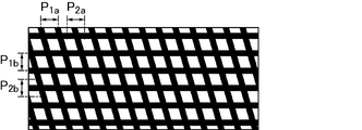
- FIG. 2 is a schematic plan view of an interference sheet (wiring of a touch panel, black matrix of a liquid crystal panel) that can be used in the first embodiment.
- FIG. 2 is a schematic plan view of an interference sheet (wiring of a touch panel, black matrix of a liquid crystal panel) that can be used in the first embodiment.
- FIG. 2 is a schematic plan view of an interference sheet (wiring of a touch panel, black matrix of a liquid crystal panel) that can be used in the first embodiment.
- FIG. 2 is a schematic plan view of an interference sheet (wiring of a touch panel, black matrix of a liquid crystal panel) that can be used in the first embodiment.
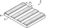
- FIG. 3 is a schematic perspective view of an interference sheet that can be used in the first embodiment.
- FIG. 3 is a schematic perspective view of an interference sheet that can be used in the first embodiment.
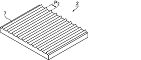
- FIG. 3 is a schematic perspective view of an interference sheet that can be used in the first embodiment.
- FIG. 3 is a schematic perspective view of an interference sheet that can be used in the first embodiment.
- FIG. 6 is a schematic cross-sectional view of a display device according to a second embodiment.
- FIG. 6 is a schematic cross-sectional view of a display device according to a third embodiment.
- the cross-sectional schematic diagram of the display apparatus X assumed in simulation.
- the cross-sectional schematic diagram of the display apparatus Y assumed in simulation.
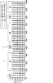
- the graph showing the simulation result of the display apparatus X The graph showing the simulation result of the display apparatus Y.
- FIG. 1 is a schematic cross-sectional view of the display device according to the first embodiment.
- FIG. 2 is a schematic perspective view of the display device according to the first embodiment.
- the touch panel 1, the interference sheet 2, and the display panel 3 are arranged in this order from the observation surface side to the back surface side.
- a capacitive touch panel is used as the touch panel 1 and a liquid crystal panel is used as the display panel 3 will be described as an example with reference to FIG. 2, but the present embodiment is not limited thereto.
- the capacitive touch panel 1 includes a transparent substrate 11 made of glass, resin, and the like, and a plurality of wirings 8 formed on the transparent substrate 11 for sensing static electricity.
- the plurality of wirings 8 may be formed of a light transmissive material or a light shielding material.
- the plurality of wirings 8 are formed with a regular pattern, but the wiring group composed of the plurality of wirings forms a lattice pattern even when forming a striped pattern when viewed as a whole. May be.
- the display panel 3 includes a first substrate 40 (color filter substrate), a second substrate 50 (array substrate), and a liquid crystal layer 60 sandwiched between the first substrate 40 and the second substrate 50.
- the first substrate 40 includes a transparent substrate 12 made of glass, resin, or the like, a black matrix 9 and a color filter 41 in order from the viewer side.
- the second substrate 50 includes a transparent substrate, a thin film transistor (TFT), a data signal line, a scanning signal line, a pixel electrode, and the like.
- the black matrix 9 is a member provided to shield a portion that is not suitable as a display unit, and is formed so as to surround one pixel, for example. Further, the black matrix 9 is formed with a certain regular pattern. However, when viewed as a whole, the black matrix 9 may form a striped pattern or a lattice pattern.
- FIGS. 6 to 9 are schematic plan views of interference sheets that can be used in the first embodiment.
- Each of the plurality of repeating units included in the interference sheet 2 may be (i) a light shielding member, or (ii) a transparent base material.
- the black-colored portion in FIGS. 6 to 9 corresponds to a portion made of a light-shielding member, while in the case of (ii), the white portion in FIGS. 6 to 9 is transparent. It corresponds to a part formed by molding a base material.
- Examples of the above (i) include a plurality of repeating units as shown in FIG. 3 when viewed in cross section.
- the plurality of repeating units shown in FIG. 3 are formed with a plurality of repeating units (light shielding portions) 4 formed of a light shielding member on the transparent substrate 5.
- Such an interference sheet 2 is manufactured by vapor deposition, photolithography etching, etc. on the transparent substrate 5 when the light-shielding member is a metal (Cu, Ag, etc.).
- 5 is manufactured by printing a light-shielding paint containing a black pigment such as carbon.
- Examples of the above (ii) include a plurality of repeating units as shown in FIG. 4 or FIG. 5 when viewed in cross section.
- the plurality of repeating units shown in FIG. 4 includes a plurality of hemispherical convex portions 6 formed by molding a transparent substrate.
- the interference sheet 2 having such a plurality of repeating units is manufactured by injection molding a resin such as acrylic or PC (polycarbonate).
- the plurality of repeating units shown in FIG. 5 are configured by forming a plurality of pointed convex portions 7 formed by forming a transparent base material in a sawtooth shape.
- the interference sheet 2 having such a plurality of repeating units is manufactured by injection molding a resin such as acrylic or PC (polycarbonate).
- a commercially available lens sheet used for a backlight can also be used.
- the repeating structure of the interference sheet examples include a striped pattern as shown in FIG. 6 or FIG. 7 or a lattice pattern as shown in FIG. 8 or FIG. It is done.
- the lattice pattern includes a plurality of repeating units (first repeating unit) parallel to each other and a plurality of other repeating units (second repeating unit) intersecting with each of the plurality of repeating units. ). It is preferable that the intervals between adjacent repeating units constituting the repeating structure are equal intervals. This is because if there is a large variation in the spacing between adjacent ones of the repeating structure, the light from the backlight unit is scattered, and the displayed image may be blurred.
- FIGS. 6 to 9 are the same as the patterns of a plurality of wirings included in the touch panel 1 and the black matrix pattern included in the liquid crystal panel.
- 6 to 9 are also schematic plan views of a plurality of wirings provided in the touch panel that can be used in the first embodiment, and are also schematic plan views of black matrices provided in the liquid crystal panel that can be used in the first embodiment.
- the blacked out portion corresponds to a wiring group.
- a blackened portion corresponds to a black matrix.
- the interval between adjacent repeating units of the interference sheet 2 is as follows.
- the distance between the centers of the light shielding portions 4 adjacent is represented by P 1.
- the distance between the tips of the convex portions 6 and 7 adjacent is represented by P 2.
- the locations serving as references for P 1 and P 2 are different between the case (i) and the case (ii).
- the interval between the centers of the adjacent light shielding portions 4 is the first interval P 1a and / or the second interval P 1b .
- the interval between the tips of the adjacent convex portions 6 and 7 is expressed by the first interval P 2a and / or the second interval P 2b .
- the interval between the centers of the adjacent light shielding portions 4 is such that at least one of the first interval P 1a and the second interval P 1b satisfies the above formula (1).
- both the first interval P 1a and the second interval P 1b satisfy the above formula (1).
- the distance between the tips of the adjacent convex portions 6 and 7 is such that at least one of the first distance P 2a and the second distance P 2b is the above formula.
- the distance of the wiring between adjacent with the touch panel 1 if wiring group constituting the stripe pattern is represented by the interval P 1 between the centers of each wire, the wiring group of the lattice-like pattern When configured, it is represented by a distance P 1a or P 1b between the centers of the wirings.
- P 1 , P 1a , and P 1b are, for example, 300 to 500 ⁇ m.
- the interval between adjacent straight line portions of the black matrix 9 included in the display panel 3 is represented by the interval P 1 between the centers of the respective straight line portions when the black matrix 9 forms a striped pattern.
- the black matrix 9 forms a lattice pattern, it is represented by the interval P 1a or P 1b between the centers of the respective straight line portions.
- all of P 1 , P 1a , and P 1b are, for example, 100 to 200 ⁇ m.
- the interference sheet 2 When the interference sheet 2 is viewed obliquely, it is represented by a schematic perspective view as shown in FIGS.
- the interference sheet shown in FIG. 10 corresponds to FIG. 3 in a schematic sectional view and FIG. 6 in a schematic plan view.
- the interference sheet shown in FIG. 11 corresponds to the cross-sectional schematic diagram of FIG. 4 and the plan schematic diagram of FIG.
- the interference sheet shown in FIG. 12 corresponds to FIG. 5 in a schematic sectional view and FIG. 6 in a schematic plan view.
- the transparent substrate examples include highly transparent resin films such as PET (polyethylene terephthalate) and TAC (triacetyl cellulose), glass, and the like.
- the light-shielding member examples include copper (Cu), iron (Fe), Examples thereof include metals such as titanium (Ti) and aluminum (Al), and resins containing black pigments.
- the interference sheet, the black matrix, the touch panel wiring that can be used in the first embodiment, and the features of the repeated structure thereof have been exemplified.
- an optimum repeating structure can be selected as appropriate.
- a liquid crystal panel including a black matrix having a plurality of straight line portions with an interval A between adjacent straight line portions and a touch panel having a plurality of wires with an interval between adjacent wire lines B are prepared.
- a gate driver, a source driver, a display control circuit, and the like are mounted on the liquid crystal panel, and a backlight unit is disposed on the back side of the liquid crystal panel.
- the selected interference sheet is inserted between the touch panel and the liquid crystal panel, and it is confirmed whether or not moire occurs visually.
- an appropriate interference sheet can be determined by replacing only the interference sheet without changing the design of the touch panel and the display panel. In this way, by observing the display device that actually incorporates the interference sheet, the influence of conditions that are difficult to include in the simulation, such as the deflection of the interference sheet and the gap between the interference sheet and the display panel, should be confirmed. Can do.
- the interference sheet selected by the simulation and examination is inserted between the touch panel and the liquid crystal display panel, thereby completing the display device.
- the moire interval may be widened or narrowed when the display device is observed from different angles. Looks.
- the gap between the display panel and the interference sheet and between the interference sheet and the touch panel is preferably narrow (specifically, 100 ⁇ m or less). It is preferable to arrange the interference sheet and the touch panel closely. Between the display panel and the interference sheet and between the touch panel and the interference sheet may or may not be fixed with an adhesive, a screw or the like.
- the interference sheet is preferably electrically connected to the ground, whereby radiation noise from the display device can be blocked and the operation of the touch panel can be stabilized.
- the second embodiment is the same as the first embodiment except that the number of interference sheets is different.
- two interference sheets 22 a and 22 b are arranged between the touch panel 21 and the display panel 23. Any of these interference sheets 22a and 22b may have the above configuration (i), or both may have the above configuration (ii). ) And one having the above configuration (ii) may be used.
- the value of the interval between adjacent repeating units of each interference sheet only needs to satisfy the above formula (1). For example, when the interval between the interference sheets 22a is Ca and the interval between the interference sheets 22b is Cb, A ⁇ Cb ⁇ Ca ⁇ B is determined.
- the moire pitch can be narrowed by inserting the interference sheet, and the moire can be made difficult to visually recognize as in the first embodiment.
- the third embodiment is the same as the first embodiment except that the number and arrangement order of interference sheets are different.
- the touch panel 31, the interference sheet 32a, the display panel 33, and the interference sheet 32b are arranged in this order from the observation surface side to the back surface side.
- Any of these interference sheets 32a and 32b may have the above-mentioned configuration (i), or both may have the above-mentioned configuration (ii). ) And one having the above configuration (ii) may be used.
- the value of the interval between the adjacent repeating structures of the interference sheets may satisfy the above formula (1). For example, when the distance between the interference sheets 32a is Cc and the distance between the interference sheets 32b is Cd, A ⁇ Cd ⁇ Cc ⁇ B.
- the moire pitch can be narrowed by inserting the interference sheet, and the moire can be made difficult to visually recognize as in the first embodiment.
- FIGS. 17 and 18 are graphs showing simulation results of the occurrence of moiré in the display devices X and Y.
- the vertical axis represents the moire contrast
- the horizontal axis represents the distance in the horizontal direction. 17 and 18 indicate the moire pitch.
- Moire can be simulated by approximating the shadow generated by the structure of the transmitted light from the backlight with a sine wave.
- the transmitted light from the backlight unit 110 causes shadows generated by a plurality of linear portions of the black matrix of the display panel 103, a plurality of wirings of the touch panel 101, and a plurality of repeating units of the interference sheet 102. These were approximated by sinusoidal waves and expressed as S AX , S BX , and S CX curves. Further, by superposing the obtained waveforms of S AX , S BX and S CX and observing the density cycle, generation of moiré that is expected to be observed when viewing the screen of the display device X can be prevented.
- the size of the period width of the waveforms of S AX , S BX and S CX is S AX ⁇ S CX ⁇ S BX .
- a is an arbitrary constant
- k 1 is the width of the straight line portion of the black matrix of the display panel
- L 1 is the distance between the adjacent straight line portions of the black matrix of the display panel
- ⁇ 1 is the display This corresponds to an error in panel layout.
- a is an arbitrary constant
- k 2 is the width of the repeating unit of the interference sheet
- L 2 is the distance between the adjacent repeating units of the interference sheet
- ⁇ 2 is an error in the arrangement of the interference sheet Equivalent to.
- when 0 ⁇ x ⁇ 180 / (a ⁇ k 3 ) + ⁇ 3 , and 180 / (a ⁇ k 3 ) + ⁇ 3 ⁇ x ⁇ 180 / (a ⁇ k 3 ) + ⁇ 3 + L 3 , it is expressed by repetition of a waveform with f (x) 0.
- a is an arbitrary constant
- k 3 is the width of the touch panel wiring
- L 3 is a distance from end to end of adjacent wirings of the touch panel
- ⁇ 3 is an error in the arrangement of the touch panel.
- the display device Y the transmitted light from the backlight unit 210, a plurality of linear portions of the black matrix of the display panel 203, the shadow generated by a plurality of lines of the touch panel 201, is approximated by each sine wave, S AY and Expressed as a S BY curve. Also, the occurrence of moire expected to be observed when viewing the screen of the display device Y was considered by superimposing the obtained waveforms of S AY and S BY and observing the density cycle. . In the display device Y, the size of the cycle width of the waveforms of S AY and S BY is S AY ⁇ S BY . S AY and S BY were calculated by the same method as S AX and S Bx .
- the simulations are as follows: (a) the width of the straight line portion of the black matrix of the display panel, the distance between the adjacent straight line portions, (b) the width of the repeating unit of the interference sheet, and the adjacent repeating unit. We examined the distance from end to end, (c) the width of the touch panel wiring, and the distance from end to end between the adjacent wirings.
- the occurrence of moire can be simulated on the same principle even if the interval is replaced with the interval between adjacent wires of the touch panel, or the interval between adjacent repeating units of the interference sheet. That is, in the display device X, when the interval between adjacent linear portions of the black matrix of the display panel is A, the interval between adjacent wirings of the touch panel is B, and the interval between adjacent repeating units of the interference sheet is C. By inserting an interference sheet satisfying A ⁇ C ⁇ B, the moire pitch can be narrowed and the moire can be made difficult to visually recognize.
- Display panel 4 Light shielding part 5: Transparent substrate 6: Convex part (Hemispherical) 7: Convex (tip is sharp) 8: Wiring 9: Black matrix 110, 210: Backlight unit 11, 12: Transparent substrate 40: First substrate (color filter substrate) 41: Color filter 50: Second substrate (array substrate) 60: Liquid crystal layer
Landscapes
- Physics & Mathematics (AREA)
- Nonlinear Science (AREA)
- Engineering & Computer Science (AREA)
- General Physics & Mathematics (AREA)
- Optics & Photonics (AREA)
- Crystallography & Structural Chemistry (AREA)
- Chemical & Material Sciences (AREA)
- Mathematical Physics (AREA)
- General Engineering & Computer Science (AREA)
- Theoretical Computer Science (AREA)
- Human Computer Interaction (AREA)
- Devices For Indicating Variable Information By Combining Individual Elements (AREA)
- Position Input By Displaying (AREA)
- Liquid Crystal (AREA)
Abstract
本発明は、タッチパネルを備えた表示装置について、タッチパネル及び表示パネルの設計の変更を必要とせずに、表示装置の透過率を維持しつつ、モアレを視認し難くする表示装置を提供する。本発明の表示装置は、互いに平行な複数の直線部を有するブラックマトリクスを備えた表示パネルと、互いに平行な複数の配線を有するタッチパネルと、互いに平行な複数の繰り返し単位を含む繰り返し構造を有する干渉シートとを備え、該タッチパネルと該表示パネルとの間に該干渉シートが配置され、該ブラックマトリクスの隣り合う直線部同士の間隔をA、該タッチパネルの隣り合う配線同士の間隔をB、該干渉シートの隣り合う繰り返し単位同士の間隔をCとすると、A<C<Bを満たすものである。
Description
本発明は、表示装置に関する。より詳しくは、タッチパネルと、表示パネルとを備える表示装置に関するものである。
近年、情報機器の操作性を高めるため、タッチパネルを備えた表示装置が提供されている。大型用のタッチパネルとしては、赤外線などの光学方式が主流であるが、静電容量方式のタッチパネルも検討されている。静電容量方式のタッチパネルには、例えば、金属細線をメッシュ状に配したメッシュタイプのタッチパネルが用いられる。
メッシュタイプのタッチパネルと表示パネルとを積層した表示装置では、規則正しく配置されたタッチパネルの金属細線と、規則正しく配置された表示パネルのブラックマトリクス等とが重ね合わせられることで干渉が起こり、モアレ(干渉縞)が発生する。モアレが発生すると、表示装置の視覚性は著しく損なわれる。
モアレの発生を低減する方法としては、光学シートの規則的パターンの形成方向と、表示パネルの画素の規則的パターンの形成方向とが成す角度を、モアレの発生が低減される角度に設定する方法が知られている。また、表示パネルの画素パターンのピッチとタッチパネルのメッシュ状に配した配線パターンのピッチを、モアレ縞の間隔が最少となるように、設定する方法が検討されている(例えば、特許文献1参照)。
近年、表示装置は薄型化に伴い、タッチパネルと表示パネルとの間隔を狭く設計する傾向にあり、モアレが発生し易くなる。上記の方法によれば、モアレの発生を低減することができるものの、表示装置ごとに、タッチパネルの配線の規則的パターンの形成方向と表示パネルの画素(すなわち、ブラックマトリクスで囲まれる領域)の規則的パターンの形成方向とが成す角度、各規則的パターンのピッチ等を設定する必要がある。そのため、表示装置に搭載する表示パネルの画素パターンが変わると、タッチパネルも再設計が必要となり、標準化が困難である。
また、表示パネルは、高い解像率を得るために表示装置の画素数を増加する傾向にあり、視野角特性を向上するために複雑な画素パターンを用いる傾向にある。一方で、メッシュタイプ等の規則的パターンを有するタッチパネルは、現状では、生産上、性能上の問題により、配線の規則的パターンのピッチは設計に制限があるため、表示パネルの画素数、画素パターン等に合わせて、モアレの発生を低減できるように設計を変更することは困難である。
更に、仮に、タッチパネルの配線の規則的パターンの形成方向と表示パネルの画素の規則的パターンの形成方向とが成す角度や、各規則的パターンのピッチを、モアレの発生を低減できるような値に設定できたとしても、生産工程で僅かにずれが生じると、モアレが発生してしまう。
本発明は、上記現状に鑑みてなされたものであり、タッチパネルを備えた表示装置について、タッチパネル及び表示パネルの設計の変更を必要とせずに、表示装置の透過率を維持しつつ、モアレを視認し難くする表示装置を提供することを目的とするものである。
本発明者は、モアレの発生を低減する方法について検討を行い、モアレピッチ(干渉縞を構成する各縞同士の間隔)を狭くすることで、モアレが視認し難くなることに着目した。また、本発明者は研究を重ねた結果、表示装置に互いに平行な一定の繰り返し構造を持つ干渉シートを挿入し、干渉の起こり方を変化させることで、発生するモアレピッチの大きさを、該干渉シートを追加する前と比較して狭くすることができることを見いだした。該方法によると、実際にはモアレは発生しているが、モアレピッチが狭いために、モアレは視認し難くなり、低減された様に感じる。
更に、上記干渉シートの隣り合う繰り返し単位の間隔が狭すぎると、表示装置の透過率が極端に下がることを見いだし、挿入する干渉シートの繰り返し単位同士の間隔を、ブラックマトリクスの隣り合う直線部同士の間隔より広く、また、タッチパネルの隣り合う配線同士の間隔より狭くすることで、表示装置の透過率を維持しつつ、モアレを視認し難くすることができることを見いだした。
こうして本発明者は、上記課題をみごとに解決することができることに想到し、本発明に到達したものである。
すなわち、本発明の一側面は、互いに平行な複数の直線部を有するブラックマトリクスを備えた表示パネルと、互いに平行な複数の配線を有するタッチパネルと、互いに平行な複数の繰り返し単位を含む繰り返し構造を有する干渉シートとを備え、該タッチパネルと該表示パネルとの間に該干渉シートが配置され、該ブラックマトリクスの隣り合う直線部同士の間隔をA、該タッチパネルの隣り合う配線同士の間隔をB、該干渉シートの隣り合う繰り返し単位同士の間隔をCとすると、下記式(1)を満たす表示装置である。

本発明の表示装置の構成としては、このような構成要素を必須として形成されるものである限り、表示装置に通常用いられるその他の構成要素を適宜適用することができる。
上記表示パネルとしては、液晶表示パネル(LCD:Liquid Crystal Display Panel)、エレクトロルミネセンス表示パネル(EL:Electroluminescence Display Panel)、プラズマディスプレイパネル(Plasma Display Panel)等が挙げられる。
表示領域内に互いに平行な複数の配線を有するタッチパネルとしては、メッシュタイプ、ストライプタイプ等のタッチパネルが挙げられ、静電容量方式のタッチパネルに適用することができる。
上記干渉シートを備えることで、干渉の起こり方を変化させ、モアレピッチを狭くして、モアレを視認し難くすることができる。
上記干渉シートの隣り合う繰り返し単位同士の間隔Cが狭すぎると、表示装置の透過率が極端に下がるため、上記式(1)を満たす干渉シートを用いることで、表示装置の透過率を維持しつつ、モアレを視認し難くすることができる。
上記干渉シートが有する複数の繰り返し単位は、例えば、遮光性の部材で構成される。遮光性の部材としては、銅(Cu)、鉄(Fe)、チタン(Ti)、アルミニウム(Al)等の金属、黒色顔料を含む樹脂等からなる部材が挙げられる。
上記干渉シートが有する複数の繰り返し単位は、例えば、透明基材を成形して成る。透明基材としては、PET(ポリエチレンテレフタレート)、TAC(トリアセチルセルロース)等の高透明樹脂フィルム、ガラス等が挙げられる。
上記干渉シートが有する繰り返し構造としては、平面視した場合に、(a)縞状パターンを構成する形態、及び、(b)格子状パターンを構成する形態が挙げられる。(a)の形態では、縞状パターンで発生するモアレを視認し難くすることができ、(b)の形態では、格子状パターンで発生するモアレを視認し難くすることができる。
上記(b)格子状パターンを構成する形態の例としては、平面視した場合に、互いに平行な複数の繰り返し単位(第一の繰り返し単位)と、該互いに平行な複数の繰り返し単位のそれぞれと交差する他の互いに平行な繰り返し単位(第二の繰り返し単位)とからなる例が挙げられる。
本発明によれば、タッチパネルを備えた表示装置について、タッチパネル及び表示パネルの設計の変更を必要とせずに、表示装置の透過率を維持しつつ、モアレを視認し難くする表示装置を提供することができる。
以下に実施形態を掲げ、本発明について図面を参照して更に詳細に説明するが、本発明はこれらの実施形態のみに限定されるものではない。
(実施形態1)
図1は、実施形態1の表示装置の断面模式図である。また、図2は、実施形態1の表示装置の斜視模式図である。図1に示すように、実施形態1では、タッチパネル1、干渉シート2及び表示パネル3が、観察面側から背面側に向かって、この順に配置されている。以下、図2を用いて、タッチパネル1として静電容量方式のタッチパネルを用い、表示パネル3として、液晶パネルを用いる場合を例として説明するが、本実施形態はこれに限定されるものではない。
図1は、実施形態1の表示装置の断面模式図である。また、図2は、実施形態1の表示装置の斜視模式図である。図1に示すように、実施形態1では、タッチパネル1、干渉シート2及び表示パネル3が、観察面側から背面側に向かって、この順に配置されている。以下、図2を用いて、タッチパネル1として静電容量方式のタッチパネルを用い、表示パネル3として、液晶パネルを用いる場合を例として説明するが、本実施形態はこれに限定されるものではない。
図2に示すように、静電容量方式のタッチパネル1は、ガラス、樹脂等からなる透明基板11と、該透明基板11上に形成された静電気を感知するための複数の配線8とを備える。複数の配線8は、透光材料で形成されても、遮光材料で形成されてもよい。また、複数の配線8は、一定の規則的パターンをもって形成されるが、該複数の配線からなる配線群は、全体として見たときに、縞状パターンを構成しても、格子状パターンを構成してもよい。
表示パネル3は、第一基板40(カラーフィルタ基板)と、第二基板50(アレイ基板)と、第一基板40及び第二基板50に挟持された液晶層60とを備える。第一基板40は、観察者側から順に、ガラス、樹脂等からなる透明基板12、ブラックマトリクス9及びカラーフィルタ41を備える。第二基板50は、透明基板、薄膜トランジスタ(TFT)、データ信号線、走査信号線、画素電極等を備える。ブラックマトリクス9は、表示部として適切でない部分を遮光するために設けられる部材であり、例えば、一つの画素を囲うように形成される。また、ブラックマトリクス9は、一定の規則パターンをもって形成されるが、全体として見たときに、縞状パターンを構成しても、格子状パターンを構成してもよい。
以下に、干渉シート2について詳しく説明する。図3~5は、実施形態1で用いられうる干渉シートの断面模式図であり、図6~9は、実施形態1で用いられうる干渉シートの平面模式図である。干渉シート2が有する複数の繰り返し単位のそれぞれは、(i)遮光性の部材で構成されたものであってもよいし、(ii)透明基材を成形して成るものであってもよい。上記(i)の場合、図6~9において黒く塗りつぶされた部分が遮光性の部材で構成された部分に相当し、一方、上記(ii)の場合、図6~9において白色の部分が透明基材が成形されて成る部分に相当する。
上記(i)の例としては、断面視した場合に、図3で示されるような複数の繰り返し単位が挙げられる。図3で示される複数の繰り返し単位は、透明基材5の上に遮光性の部材で形成された複数の繰り返し単位(遮光部分)4が形成されている。このような干渉シート2は、遮光性の部材が金属(Cu、Ag等)の場合は、透明基材5上に、蒸着、フォトリソエッチング等することによって製造され、樹脂の場合は、透明基材5上に、カーボン等の黒色顔料を含む遮光性のある塗料を印刷して製造される。
上記(ii)の例としては、断面視した場合に、図4又は図5で示されるような複数の繰り返し単位が挙げられる。図4で示される複数の繰り返し単位は、透明基材を成形して成る、半球状の複数の凸部6で構成される。このような複数の繰り返し単位を有する干渉シート2は、アクリルやPC(ポリカーボネート)などの樹脂を射出成型することによって製造される。一方、図5で示される複数の繰り返し単位は、透明基材を成形して成る、先の尖った複数の凸部7がノコギリ歯状に並んで構成される。このような複数の繰り返し単位を有する干渉シート2は、アクリルやPC(ポリカーボネート)などの樹脂を射出成型することによって製造される。なお、干渉シート2としては、バックライトに用いられる市販のレンズシートを用いることもできる。
上記干渉シートが有する繰り返し構造の例としては、平面視した場合に、図6若しくは図7で示されるような縞状パターン、又は、図8若しくは図9で示されるような、格子状パターンが挙げられる。該格子状パターンは、言い換えれば、互いに平行な複数の繰り返し単位(第一の繰り返し単位)と、該複数の繰り返し単位のそれぞれと交差する他の互いに平行な複数の繰り返し単位(第二の繰り返し単位)とからなる。繰り返し構造を構成する互いに平行な繰り返し単位の隣り合うもの同士の間隔は、それぞれ等間隔であることが好ましい。繰り返し構造の隣り合うもの同士の間隔のばらつきが大きいと、バックライトユニットからの光が散乱し、表示される映像がぼやけてしまうおそれがあるためである。
図6~図9で示されるパターンは、更に、タッチパネル1が有する複数の配線のパターン、及び、液晶パネルが有するブラックマトリクスのパターンとも同様である。すなわち、図6~図9は、実施形態1で用いられうるタッチパネルが備える複数の配線の平面模式図でもあり、実施形態1で用いられうる液晶パネルが備えるブラックマトリクスの平面模式図でもある。図6~9がタッチパネルを表すときは、黒く塗りつぶされた部分が配線群に相当する。また、図6~9が液晶パネルを表すときは、黒く塗りつぶされた部分がブラックマトリクスに相当する。
干渉シート2が有する隣り合う繰り返し単位同士の間隔とは、以下のとおりである。上記(i)の場合は、図3に示すように、隣り合う遮光部分4の中心同士の間隔は、P1で表される。上記(ii)の場合は、図4及び図5に示すように、隣り合う凸部6、7の先端同士の間隔は、P2で表される。平面視においては、縞状パターンでは、図6及び図7に示すように、上記(i)の場合と上記(ii)の場合とで、P1及びP2の基準となる場所が異なる。格子状パターンでは、図8及び図9に示すように、上記(i)の場合、隣り合う遮光部分4の中心同士の間隔は、第一の間隔P1a及び/又は第二の間隔P1bで表され、上記(ii)の場合、隣り合う凸部6、7の先端同士の間隔は、第一の間隔P2a及び/又は第二の間隔P2bで表される。格子状のパターンにおいて、上記(i)の場合、隣り合う遮光部分4の中心同士の間隔は、第一の間隔P1a及び第二の間隔P1bの少なくとも一方が、上記式(1)を満たしていればよいが、第一の間隔P1a及び第二の間隔P1bのいずれもが上記式(1)を満たしていることがより好ましい。同様に、格子状のパターンにおいて、上記(ii)の場合、隣り合う凸部6、7の先端同士の間隔は、第一の間隔P2a及び第二の間隔P2bの少なくとも一方が、上記式(1)を満たしていればよいが、第一の間隔P2a及び第二の間隔P2bのいずれもが上記式(1)を満たしていることがより好ましい。
例えば、32型4K2K(画素数:4096×2160)の液晶パネルと併せて使用する場合、干渉シート2が有する隣り合う繰り返し単位同士の間隔の具体的な大きさとしては、P1、P1a、P1b、P2、P2a、P2bのいずれも、例えば、200~300μmである。
同様に、タッチパネル1が有する隣り合う配線同士の間隔は、該配線群が縞状パターンを構成する場合は、各配線の中心同士の間隔P1で表わされ、該配線群が格子状パターンを構成する場合は、各配線の中心同士の間隔P1a又はP1bで表わされる。タッチパネル1が有する隣り合う配線同士の間隔の具体的な大きさとしては、P1、P1a、P1bのいずれも、例えば、300~500μmである。
同様に、表示パネル3が有するブラックマトリクス9の隣り合う直線部同士の間隔は、該ブラックマトリクス9が縞状パターンを構成する場合は、各直線部の中心同士の間隔P1で表わされ、該ブラックマトリクス9が格子状パターンを構成する場合は、各直線部の中心同士の間隔P1a又はP1bで表わされる。ブラックマトリクス9が有する隣り合う直線部同士の間隔の具体的な大きさとしては、P1、P1a、P1bのいずれも、例えば、100~200μmである。
干渉シート2を斜めから見たときには、図10~12のような斜視模式図で表される。図10に示す干渉シートは、断面模式図が図3、平面模式図が図6に対応する。図11に示す干渉シートは、断面模式図が図4、平面模式図が図6に対応する。図12に示す干渉シートは、断面模式図が図5、平面模式図が図6に対応する。
上記透明基材としては、PET(ポリエチレンテレフタレート)、TAC(トリアセチルセルロース)等の高透明樹脂フィルム、ガラス等が挙げられ、上記遮光性の部材としては、銅(Cu)、鉄(Fe)、チタン(Ti)、アルミニウム(Al)等の金属、黒色顔料を含む樹脂等が挙げられる。
以上、実施形態1で用いることができる干渉シート、ブラックマトリクス及びタッチパネルの配線並びにその繰り返し構造の特徴について例示したが、この限りではなく、表示装置及びタッチパネルの構造に起因して発生するモアレの形状、モアレピッチ等に応じて、適宜、最適な繰り返し構造を選択することができる。
以下に、実施形態1の表示装置の製造工程について説明する。
まず、隣り合う直線部同士の間隔がAである複数の直線部を有するブラックマトリクスを備える液晶パネル、及び、隣り合う配線同士の間隔がBである複数の配線を有するタッチパネルを用意する。次に、液晶パネルに対し、ゲートドライバー、ソースドライバー、表示制御回路等を実装するとともに、液晶パネルの背面側にバックライトユニットを配置する。
次に、A及びBの具体的な値を設定し、干渉シートの隣り合う繰り返し単位同士の間隔Cが下記式(1)を満たす干渉シートを選抜する。

次に、選抜した干渉シートを上記タッチパネルと上記液晶パネルとの間に挿入し、目視でモアレが発生するか否かを確認する。このとき、ブラックマトリクスが有する複数の直線部、タッチパネルが有する複数の配線、及び、干渉シートが有する繰り返し構造の繰り返し単位が平行となるように配置することで、より干渉縞が発生し易くなり、より効果的にモアレを視認し難くすることができる。
モアレの発生が低減されない場合は、上記式(1)を満たす他の干渉シートを挿入し、再度検討を行う。この際、タッチパネル及び表示パネルの設計を変更することなく、干渉シートのみを交換することで、適切な干渉シートを決定することができる。このように、実際に干渉シートを組み込んだ表示装置を観察することで、干渉シートのたわみや、干渉シートと表示パネルとの間隙等、シミュレーションには含めることが難しい条件の影響を、確認することができる。
モアレが視認され難いことを確認した後、上記タッチパネルと上記液晶表示パネルとの間に、上記シミュレーション及び検討により選抜した干渉シートを挿し込み、表示装置が完成する。
表示装置の組み立て工程において、表示パネルと干渉シートの間、及び干渉シートとタッチパネルとの間の間隙が広いと、表示装置を異なる角度から観察した場合に、モアレの間隔が、広がったり狭まったりして見える。このようなモアレの変化を低減するためには、表示パネルと干渉シートの間、及び、干渉シートとタッチパネルとの間の間隙は狭い(具体的には、100μm以下)ことが好ましく、表示パネル、干渉シート及びタッチパネルは、密接して配置することが好ましい。表示パネルと干渉シートとの間、及び、タッチパネルと干渉シートとの間は、接着剤、ビス等で固定されていてもよいし、されていなくてもよい。
また、上記干渉シートは、電気的にグラウンドに接続しておくことが好ましく、これにより、表示装置からの輻射ノイズを遮断することができ、タッチパネルの動作を安定させることができる。
(実施形態2)
実施形態2は、干渉シートの枚数が異なる点以外は、実施形態1と同様である。実施形態2では、図13に示すように、タッチパネル21と表示パネル23との間に、二枚の干渉シート22a及び22bが配置されている。これらの干渉シート22a及び22bは、いずれもが上記(i)の構成を有するものであってもよいし、いずれもが上記(ii)の構成を有するものであってもよいし、上記(i)の構成を有するものと上記(ii)の構成を有するものとがそれぞれ1枚ずつ用いられたものであってもよい。本実施形態のように、干渉シートを複数枚挿入する場合には、各干渉シートの隣り合う繰り返し単位の間隔の値が、上記式(1)を満たせばよい。例えば、干渉シート22aの間隔をCa、干渉シート22bの間隔をCbとすると、A<Cb<Ca<Bで決定される。
実施形態2は、干渉シートの枚数が異なる点以外は、実施形態1と同様である。実施形態2では、図13に示すように、タッチパネル21と表示パネル23との間に、二枚の干渉シート22a及び22bが配置されている。これらの干渉シート22a及び22bは、いずれもが上記(i)の構成を有するものであってもよいし、いずれもが上記(ii)の構成を有するものであってもよいし、上記(i)の構成を有するものと上記(ii)の構成を有するものとがそれぞれ1枚ずつ用いられたものであってもよい。本実施形態のように、干渉シートを複数枚挿入する場合には、各干渉シートの隣り合う繰り返し単位の間隔の値が、上記式(1)を満たせばよい。例えば、干渉シート22aの間隔をCa、干渉シート22bの間隔をCbとすると、A<Cb<Ca<Bで決定される。
実施形態2の表示装置においても、干渉シートを挿入することで、モアレピッチを狭くすることができ、実施形態1と同様に、モアレを視認し難くすることができる。
(実施形態3)
実施形態3は、干渉シートの枚数及び配置順が異なる点以外は、実施形態1と同様である。実施形態3では、図14に示すように、タッチパネル31、干渉シート32a、表示パネル33及び干渉シート32bが、観察面側から背面側に向かって、この順に配置されている。これらの干渉シート32a及び32bは、いずれもが上記(i)の構成を有するものであってもよいし、いずれもが上記(ii)の構成を有するものであってもよいし、上記(i)の構成を有するものと上記(ii)の構成を有するものとがそれぞれ1枚ずつ用いられたものであってもよい。本実施形態のように、表示パネルの上下にそれぞれ干渉シートを挿入する場合には、各干渉シートの隣り合う繰り返し構造の間隔の値が、上記式(1)を満たせばよい。例えば、干渉シート32aの間隔をCc、干渉シート32bの間隔をCdとすると、A<Cd<Cc<Bで決定される。
実施形態3は、干渉シートの枚数及び配置順が異なる点以外は、実施形態1と同様である。実施形態3では、図14に示すように、タッチパネル31、干渉シート32a、表示パネル33及び干渉シート32bが、観察面側から背面側に向かって、この順に配置されている。これらの干渉シート32a及び32bは、いずれもが上記(i)の構成を有するものであってもよいし、いずれもが上記(ii)の構成を有するものであってもよいし、上記(i)の構成を有するものと上記(ii)の構成を有するものとがそれぞれ1枚ずつ用いられたものであってもよい。本実施形態のように、表示パネルの上下にそれぞれ干渉シートを挿入する場合には、各干渉シートの隣り合う繰り返し構造の間隔の値が、上記式(1)を満たせばよい。例えば、干渉シート32aの間隔をCc、干渉シート32bの間隔をCdとすると、A<Cd<Cc<Bで決定される。
実施形態3の表示装置においても、干渉シートを挿入することで、モアレピッチを狭くすることができ、実施形態1と同様に、モアレを視認し難くすることができる。
(評価試験)
干渉シートを有する表示装置(以下、表示装置Xともいう。)と、干渉シートを有さない表示装置(以下、表示装置Yともいう。)におけるモアレの発生について、評価試験を行った。
干渉シートを有する表示装置(以下、表示装置Xともいう。)と、干渉シートを有さない表示装置(以下、表示装置Yともいう。)におけるモアレの発生について、評価試験を行った。
図15及び図16は、それぞれ、シミュレーションにおいて想定した表示装置X及びYの構成を示す断面模式図である。表示装置Xは、図15に示すように、タッチパネル101、干渉シート102、表示パネル103及びバックライトユニット110が、観察面側から背面側に向かって、この順に配置された構成を有する。表示装置Yは、図16に示すように、タッチパネル201、表示パネル203及びバックライトユニット210が、観察面側から背面側に向かって、この順に配置された構成を有する。図17及び図18は、表示装置X及びYのモアレ発生の各シミュレーション結果を表すグラフである。図17及び図18において、縦軸はモアレコントラスト、横軸は横方向の距離を表す。図17及び図18中の横向きの両矢印は、モアレピッチを表す。
モアレは、バックライトからの透過光が構造物に起因して発生する影を、正弦波で近似することでシミュレートすることができる。
表示装置Xについては、バックライトユニット110からの透過光が、表示パネル103のブラックマトリクスの複数の直線部、タッチパネル101の複数の配線、及び、干渉シート102の複数の繰り返し単位によって発生する影を、それぞれ正弦波で近似し、SAX、SBX、SCXの曲線として表した。また、得られたSAX、SBX及びSCXの波形を重ね合わせ、その疎密の周期を観察することで、表示装置Xの画面を見たときに観察されると予想されるモアレの発生を考察した。表示装置Xでは、SAX、SBX及びSCXの波形の周期幅の大きさは、SAX<SCX<SBXである。
SAXは、0<x<180/(a×k1)+φ1の時、f(x)=|sin(a×k1×x-φ1)|であり、180/(a×k1)+φ1<x<180/(a×k1)+φ1+L1の時、f(x)=0である波形の繰り返しで表される。aは、任意の定数、k1は、表示パネルのブラックマトリクスの直線部の幅、L1は、表示パネルのブラックマトリクスの隣り合う直線部同士の端から端までの距離、φ1は、表示パネルの配置の誤差に相当する。
SBXは、0<x<180/(a×k2)+φの時、f(x)=|sin(a×k2×x-φ2)|であり、180/(a×k2)+φ2<x<180/(a×k2)+φ2+L2の時、f(x)=0である波形の繰り返しで表される。aは、任意の定数、k2は、干渉シートの繰り返し単位の幅、L2は、干渉シートの隣り合う繰り返し単位同士の端から端までの距離、φ2は、干渉シートの配置の誤差に相当する。
SCXは、0<x<180/(a×k3)+φ3の時、f(x)=|sin(a×k3×x-φ3)|であり、180/(a×k3)+φ3<x<180/(a×k3)+φ3+L3の時、f(x)=0である波形の繰り返しで表される。aは、任意の定数、k3は、タッチパネルの配線の幅、L3は、タッチパネルの隣り合う配線同士の端から端までの距離、φ3は、タッチパネルの配置の誤差に相当する。
表示装置Yについては、バックライトユニット210からの透過光が、表示パネル203のブラックマトリクスの複数の直線部、タッチパネル201の複数の配線によって発生する影を、それぞれ正弦波で近似し、SAY及びSBYの曲線として表した。また、得られた、SAY及びSBYの波形を重ね合わせ、その疎密の周期を観察することで、表示装置Yの画面を見たときに観察されると予想されるモアレの発生を考察した。表示装置Yでは、SAY及びSBYの波形の周期幅の大きさは、SAY<SBYである。SAY、SBYは、上記SAX、SBxと同様の方法で算出した。
図17と図18とを比較すると、図18に示すように、干渉シートを有さない表示装置Yでは、SAyとSByが密に現れる部分と、疎で現れる部分が、周期的に観察され、疎密の周期幅は広い。そのため、モアレピッチは広くなり、モアレは視認し易いと考えられる。一方、図17に示すように、干渉シートを有する表示装置Xでは、SAx、SBx及びSCxが密に現れる部分と、疎で現れる部分が、周期的に観察され、疎密の周期幅は、表示装置Yの場合よりも狭い。そのため、表示装置Xは、表示装置Yと比較して、モアレピッチは狭くなり、モアレは視認し難いと考えられる。
以上のシミュレーション結果から、SAX、SBX及びSCXの波形の周期幅の大きさが、SAX<SCX<SBXとなるような、干渉シートを挿入することでモアレピッチを狭くすることができ、モアレを視認し難くすることができることが分かった。上記シミュレーションは、(イ)表示パネルのブラックマトリクスの直線部の幅、及び、隣り合う直線部同士の端から端までの距離、(ロ)干渉シートの繰り返し単位の幅、及び、隣り合う繰り返し単位同士の端から端までの距離、(ハ)タッチパネルの配線の幅、及び、隣り合う配線同士の端から端までの距離に着目し検討を行ったが、表示パネルのブラックマトリクスの隣り合う直線部同士の間隔、タッチパネルの隣り合う配線同士の間隔、干渉シートの隣り合う繰り返し単位同士の間隔に置き換えたとしても同様の原理で、モアレの発生をシミュレートすることができる。すなわち、表示装置Xにおいて、表示パネルのブラックマトリクスの隣り合う直線部同士の間隔をA、タッチパネルの隣り合う配線同士の間隔をB、干渉シートの隣り合う繰り返し単位同士の間隔をCとした場合に、A<C<Bを満たす干渉シートを挿入することで、モアレピッチを狭くすることができ、モアレを視認し難くすることができる。
1、21、31、101、201:タッチパネル
2、22a、22b、32a、32b、102:干渉シート
3、23、33、103、203:表示パネル
4:遮光部分
5:透明基材
6:凸部(半球状)
7:凸部(先端が尖っている)
8:配線
9:ブラックマトリクス
110、210:バックライトユニット
11、12:透明基板
40:第一基板(カラーフィルタ基板)
41:カラーフィルタ
50:第二基板(アレイ基板)
60:液晶層
2、22a、22b、32a、32b、102:干渉シート
3、23、33、103、203:表示パネル
4:遮光部分
5:透明基材
6:凸部(半球状)
7:凸部(先端が尖っている)
8:配線
9:ブラックマトリクス
110、210:バックライトユニット
11、12:透明基板
40:第一基板(カラーフィルタ基板)
41:カラーフィルタ
50:第二基板(アレイ基板)
60:液晶層
Claims (5)
- 互いに平行な複数の直線部を有するブラックマトリクスを備えた表示パネルと、
互いに平行な複数の配線を有するタッチパネルと、
互いに平行な複数の繰り返し単位を含む繰り返し構造を有する干渉シートとを備え、
該タッチパネルと該表示パネルとの間に該干渉シートが配置され、
該ブラックマトリクスの隣り合う直線部同士の間隔をA、該タッチパネルの隣り合う配線同士の間隔をB、該干渉シートの隣り合う繰り返し単位同士の間隔をCとすると、下記式(1)を満たすことを特徴とする表示装置。

- 前記干渉シートが有する複数の繰り返し単位は、遮光性の部材で構成されることを特徴とする請求項1に記載の表示装置。
- 前記干渉シートが有する複数の繰り返し単位は、透明基材を成形して成ることを特徴とする請求項1に記載の表示装置。
- 前記干渉シートが有する繰り返し構造は、平面視した場合に、縞状パターンを構成することを特徴とする請求項1~3のいずれかに記載の表示装置。
- 前記干渉シートが有する繰り返し構造は、平面視した場合に、格子状パターンを構成し、
該格子状パターンは、前記互いに平行な複数の繰り返し単位と、該複数の繰り返し単位のそれぞれと交差する他の互いに平行な複数の繰り返し単位とからなる
することを特徴とする請求項1~3のいずれかに記載の表示装置。
Priority Applications (1)
| Application Number | Priority Date | Filing Date | Title |
|---|---|---|---|
| US14/422,046 US20150241728A1 (en) | 2012-08-31 | 2013-08-22 | Display device |
Applications Claiming Priority (2)
| Application Number | Priority Date | Filing Date | Title |
|---|---|---|---|
| JP2012192163 | 2012-08-31 | ||
| JP2012-192163 | 2012-08-31 |
Publications (1)
| Publication Number | Publication Date |
|---|---|
| WO2014034513A1 true WO2014034513A1 (ja) | 2014-03-06 |
Family
ID=50183328
Family Applications (1)
| Application Number | Title | Priority Date | Filing Date |
|---|---|---|---|
| PCT/JP2013/072381 Ceased WO2014034513A1 (ja) | 2012-08-31 | 2013-08-22 | 表示装置 |
Country Status (2)
| Country | Link |
|---|---|
| US (1) | US20150241728A1 (ja) |
| WO (1) | WO2014034513A1 (ja) |
Cited By (2)
| Publication number | Priority date | Publication date | Assignee | Title |
|---|---|---|---|---|
| US20180188590A1 (en) * | 2017-01-05 | 2018-07-05 | Boe Technology Group Co., Ltd. | Touch display screen and method for manufacturing the same, touch display device |
| EP3343331A4 (en) * | 2015-07-30 | 2019-05-01 | Boe Technology Group Co. Ltd. | DISPLAY PANEL, TOUCH INDICATOR AND DISPLAY PANEL MANUFACTURING METHOD |
Families Citing this family (2)
| Publication number | Priority date | Publication date | Assignee | Title |
|---|---|---|---|---|
| CN105094433B (zh) * | 2015-08-12 | 2018-09-04 | 京东方科技集团股份有限公司 | 显示基板和显示装置 |
| CN210222424U (zh) * | 2019-09-23 | 2020-03-31 | 北京京东方显示技术有限公司 | 显示面板及显示装置 |
Citations (7)
| Publication number | Priority date | Publication date | Assignee | Title |
|---|---|---|---|---|
| JPH03120037A (ja) * | 1989-10-04 | 1991-05-22 | Sanyo Kokusaku Pulp Co Ltd | 積層体の干渉縞発生防止方法及び干渉縞の発生を防止した積層体 |
| JP2002313121A (ja) * | 2001-04-16 | 2002-10-25 | Nitto Denko Corp | タッチパネル付照明装置及び反射型液晶表示装置 |
| JP2005018726A (ja) * | 2002-10-16 | 2005-01-20 | Alps Electric Co Ltd | 透明座標入力装置および透明複合材 |
| JP2006162922A (ja) * | 2004-12-07 | 2006-06-22 | Seiko Epson Corp | 電気光学装置および電子機器 |
| JP2008083463A (ja) * | 2006-09-28 | 2008-04-10 | Hitachi Displays Ltd | 表示装置 |
| JP2008134489A (ja) * | 2006-11-29 | 2008-06-12 | Sharp Corp | 表示装置 |
| JP2009020294A (ja) * | 2007-07-11 | 2009-01-29 | Sharp Corp | 表示装置 |
Family Cites Families (2)
| Publication number | Priority date | Publication date | Assignee | Title |
|---|---|---|---|---|
| WO2010137376A1 (ja) * | 2009-05-29 | 2010-12-02 | シャープ株式会社 | 液晶表示装置 |
| US8599150B2 (en) * | 2009-10-29 | 2013-12-03 | Atmel Corporation | Touchscreen electrode configuration |
-
2013
- 2013-08-22 WO PCT/JP2013/072381 patent/WO2014034513A1/ja not_active Ceased
- 2013-08-22 US US14/422,046 patent/US20150241728A1/en not_active Abandoned
Patent Citations (7)
| Publication number | Priority date | Publication date | Assignee | Title |
|---|---|---|---|---|
| JPH03120037A (ja) * | 1989-10-04 | 1991-05-22 | Sanyo Kokusaku Pulp Co Ltd | 積層体の干渉縞発生防止方法及び干渉縞の発生を防止した積層体 |
| JP2002313121A (ja) * | 2001-04-16 | 2002-10-25 | Nitto Denko Corp | タッチパネル付照明装置及び反射型液晶表示装置 |
| JP2005018726A (ja) * | 2002-10-16 | 2005-01-20 | Alps Electric Co Ltd | 透明座標入力装置および透明複合材 |
| JP2006162922A (ja) * | 2004-12-07 | 2006-06-22 | Seiko Epson Corp | 電気光学装置および電子機器 |
| JP2008083463A (ja) * | 2006-09-28 | 2008-04-10 | Hitachi Displays Ltd | 表示装置 |
| JP2008134489A (ja) * | 2006-11-29 | 2008-06-12 | Sharp Corp | 表示装置 |
| JP2009020294A (ja) * | 2007-07-11 | 2009-01-29 | Sharp Corp | 表示装置 |
Cited By (2)
| Publication number | Priority date | Publication date | Assignee | Title |
|---|---|---|---|---|
| EP3343331A4 (en) * | 2015-07-30 | 2019-05-01 | Boe Technology Group Co. Ltd. | DISPLAY PANEL, TOUCH INDICATOR AND DISPLAY PANEL MANUFACTURING METHOD |
| US20180188590A1 (en) * | 2017-01-05 | 2018-07-05 | Boe Technology Group Co., Ltd. | Touch display screen and method for manufacturing the same, touch display device |
Also Published As
| Publication number | Publication date |
|---|---|
| US20150241728A1 (en) | 2015-08-27 |
Similar Documents
| Publication | Publication Date | Title |
|---|---|---|
| JP6503728B2 (ja) | 表示装置 | |
| CN104428738B (zh) | 触摸板传感器、触摸板装置以及显示装置 | |
| KR102405198B1 (ko) | 감소된 모아레 패턴들을 갖는 터치 디스플레이 시스템 | |
| CN104090673B (zh) | 具有低可见度导体的触屏传感器 | |
| US20140332256A1 (en) | Micro-wire electrode structure having non-linear gaps | |
| US10055832B2 (en) | Conductive film, display device having the same, and method of evaluating conductive film | |
| KR101301480B1 (ko) | 터치스크린 센서, 이를 구비하는 영상 표시 장치 및 그 제조 방법 | |
| JP6511382B2 (ja) | 導電性フィルム、及びこれを備える表示装置 | |
| KR101961259B1 (ko) | 도전성 필름, 이것을 구비하는 표시 장치 및 도전성 필름의 평가 방법 | |
| EP2743764B1 (en) | Method of designing random pattern and apparatus for designing random pattern | |
| JP6451258B2 (ja) | タッチパネル用電極基板、及びタッチパネル、ならびに表示装置 | |
| KR101878250B1 (ko) | 도전성 필름, 이것을 구비하는 표시 장치 및 도전성 필름의 평가 방법 | |
| KR101615949B1 (ko) | 도전성 필름 및 그것을 구비하는 터치 패널과 표시 장치 | |
| WO2018166189A1 (en) | Touch panel, mutual capacitive touch screen, and touch display device | |
| CN106990868B (zh) | 触控显示装置 | |
| US20210351253A1 (en) | Electronic Device and Display Apparatus | |
| EP3477448B1 (en) | Touch panel, and display device | |
| JPWO2014097921A1 (ja) | 表示装置及び導電性フイルムのパターンの決定方法 | |
| TWI619052B (zh) | 觸摸板 | |
| CN101122684A (zh) | 无莫尔纹的立体显示装置及方法 | |
| JP6015203B2 (ja) | タッチパネル用電極基材、及びタッチパネル、並びに画像表示装置 | |
| WO2014034513A1 (ja) | 表示装置 | |
| CN106896553A (zh) | 具有触控感测功能的显示装置 | |
| JP6265021B2 (ja) | タッチパネルセンサ、タッチパネル装置および表示装置 | |
| JP6477079B2 (ja) | タッチパネルセンサ、タッチパネル装置および表示装置 |
Legal Events
| Date | Code | Title | Description |
|---|---|---|---|
| 121 | Ep: the epo has been informed by wipo that ep was designated in this application |
Ref document number: 13832966 Country of ref document: EP Kind code of ref document: A1 |
|
| WWE | Wipo information: entry into national phase |
Ref document number: 14422046 Country of ref document: US |
|
| NENP | Non-entry into the national phase |
Ref country code: DE |
|
| 122 | Ep: pct application non-entry in european phase |
Ref document number: 13832966 Country of ref document: EP Kind code of ref document: A1 |
|
| NENP | Non-entry into the national phase |
Ref country code: JP |