WO2014034504A1 - 基板ステージ及びそれを備えた基板処理装置 - Google Patents
基板ステージ及びそれを備えた基板処理装置 Download PDFInfo
- Publication number
- WO2014034504A1 WO2014034504A1 PCT/JP2013/072344 JP2013072344W WO2014034504A1 WO 2014034504 A1 WO2014034504 A1 WO 2014034504A1 JP 2013072344 W JP2013072344 W JP 2013072344W WO 2014034504 A1 WO2014034504 A1 WO 2014034504A1
- Authority
- WO
- WIPO (PCT)
- Prior art keywords
- substrate
- stage
- spin chuck
- substrate stage
- mounting surface
- Prior art date
- Legal status (The legal status is an assumption and is not a legal conclusion. Google has not performed a legal analysis and makes no representation as to the accuracy of the status listed.)
- Ceased
Links
Images



Classifications
-
- H—ELECTRICITY
- H10—SEMICONDUCTOR DEVICES; ELECTRIC SOLID-STATE DEVICES NOT OTHERWISE PROVIDED FOR
- H10P—GENERIC PROCESSES OR APPARATUS FOR THE MANUFACTURE OR TREATMENT OF DEVICES COVERED BY CLASS H10
- H10P72/00—Handling or holding of wafers, substrates or devices during manufacture or treatment thereof
- H10P72/70—Handling or holding of wafers, substrates or devices during manufacture or treatment thereof for supporting or gripping
- H10P72/78—Handling or holding of wafers, substrates or devices during manufacture or treatment thereof for supporting or gripping using vacuum or suction, e.g. Bernoulli chucks
-
- H—ELECTRICITY
- H10—SEMICONDUCTOR DEVICES; ELECTRIC SOLID-STATE DEVICES NOT OTHERWISE PROVIDED FOR
- H10P—GENERIC PROCESSES OR APPARATUS FOR THE MANUFACTURE OR TREATMENT OF DEVICES COVERED BY CLASS H10
- H10P72/00—Handling or holding of wafers, substrates or devices during manufacture or treatment thereof
- H10P72/70—Handling or holding of wafers, substrates or devices during manufacture or treatment thereof for supporting or gripping
- H10P72/76—Handling or holding of wafers, substrates or devices during manufacture or treatment thereof for supporting or gripping using mechanical means, e.g. clamps or pinches
- H10P72/7604—Handling or holding of wafers, substrates or devices during manufacture or treatment thereof for supporting or gripping using mechanical means, e.g. clamps or pinches the wafers being placed on a susceptor, stage or support
- H10P72/7614—Handling or holding of wafers, substrates or devices during manufacture or treatment thereof for supporting or gripping using mechanical means, e.g. clamps or pinches the wafers being placed on a susceptor, stage or support characterised by a plurality of individual support members, e.g. support posts or protrusions
Definitions
- the present invention relates to a substrate stage on which a substrate is placed, and a substrate processing apparatus including the substrate stage.
- a photolithography technique is generally used.
- a process of applying a photoresist solution to the substrate to form a resist film, exposing the resist film to a predetermined circuit pattern, and then performing a development process is performed.
- the substrate when performing substrate processing such as application or development of a photoresist solution, the substrate is placed in a vacuum-sucked state on a rotatable substrate stage called a spin chuck stage.
- a spin chuck stage When the photoresist solution is applied and the substrate is rotated, the substrate is frictionally charged. Further, when the substrate is peeled from the spin chuck stage after the substrate processing, the substrate is peeled and charged.
- the charge charged on the substrate in this manner becomes a problem because it causes electrostatic breakdown of an element (for example, a thin film transistor) formed on the substrate surface.
- Patent Document 1 Measures against electrostatic breakdown described above are disclosed in, for example, Patent Document 1 and Patent Document 2.
- Japanese Patent Application Laid-Open No. 2004-133620 discloses a configuration in which a charged substrate is neutralized during a process of forming a coating film using ions generated by an ionizer. In this configuration, the air generated by the blower mechanism is used to transport ions generated by the ionizer to the substrate.
- Patent Document 2 discloses a configuration in which an amorphous alumina film is formed by anodization after a predetermined emboss shape is formed on a substrate mounting surface in a substrate stage.
- the amorphous alumina film is dense and strong, and therefore functions as a film for preventing peeling electrification. Further, it is said that a good temperature distribution can be obtained while preventing exfoliation charging by forming an embossed shape on the mounting surface in association with the formation of an alumina film.
- Patent Document 1 is an effective method as a countermeasure against electrostatic breakdown, but the applicant's research has revealed that the countermeasure against electrostatic breakdown may not be sufficient even with this configuration.
- a substrate stage according to the present invention includes a placement surface on which a substrate is placed, a suction groove provided on the placement surface, for sucking the substrate, and a placement surface. It has a configuration (first configuration) including a plurality of fine irregularities provided at random in at least a part.
- the substrate stage having this configuration does not need to form an alumina film on the mounting surface, can simplify the structure, and can be manufactured at low cost.
- the substrate stage having the first configuration may be configured to be rotatable (second configuration). This configuration can be applied to, for example, a coating apparatus.
- the substrate stage having the first or second configuration it is preferable to adopt a configuration (third configuration) in which fine unevenness is not provided on the outermost peripheral portion of the mounting surface. According to this configuration, leakage can be prevented when the substrate is sucked using the suction groove.
- the Ra (arithmetic mean roughness) of the region where the fine unevenness is provided is 0.6 ⁇ m or more and 1.0 ⁇ m or less (fourth) Is preferable. According to this configuration, for example, even when the substrate stage rotates at a high speed (for example, 1000 rpm or more), the possibility that the substrate is peeled off from the substrate stage can be reduced.
- the substrate stage having any one of the first to fourth configurations may have a configuration (fifth configuration) in which the fine unevenness is provided over substantially the entire area of the mounting surface. According to this configuration, the contact area between the substrate placed on the placement surface and the substrate stage is reduced as much as possible, and the amount that the substrate is charged when the substrate is separated from the placement surface (charge amount of the substrate) It is easy to suppress.
- the substrate stage having any one of the first to fourth configurations may have a configuration (sixth configuration) in which the fine unevenness is provided in a part of the mounting surface.
- the partial range of the mounting surface is about 1/3 to 1/2 of the entire mounting surface.
- the partial range may include a plurality of annular regions (seventh configuration) formed concentrically at intervals.
- the substrate stage having any one of the first to seventh configurations may further include a lateral shift prevention unit for preventing lateral displacement of the substrate (eighth configuration). According to this configuration, it is possible to reduce the possibility that the substrate peels off from the substrate stage when the substrate stage rotates at a high speed.
- the fine irregularities have a configuration (9th configuration) formed by blasting. According to this configuration, it is easy to obtain a large number of irregularities on the mounting surface at random.
- the present invention has a configuration (tenth configuration) which is a substrate processing apparatus including the substrate stage having any one of the first to ninth configurations.
- a configuration which is a substrate processing apparatus including the substrate stage having any one of the first to ninth configurations.
- an element for example, a thin film transistor
- Examples of the substrate processing apparatus include a coating apparatus and a developing apparatus.
- the substrate processing apparatus having the tenth configuration may further include a configuration (eleventh configuration) further including a rotating unit that rotates the substrate stage and a decompression unit that depressurizes the suction groove.
- a configuration (eleventh configuration) further including a rotating unit that rotates the substrate stage and a decompression unit that depressurizes the suction groove.
- the present invention it is possible to suppress the charging of the substrate due to peeling, and to provide a substrate stage with a simple configuration.
- a substrate processing apparatus that includes such a substrate stage and is appropriately provided with countermeasures against electrostatic discharge.
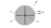
- FIG. 1 is a schematic plan view when a substrate stage (spin chuck stage) according to a first embodiment of the present invention is viewed from above.
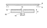
- FIG. 5 is a schematic cross-sectional view for explaining the relationship between the spin chuck stage and the substrate, showing a state before the substrate is placed on the spin chuck stage.
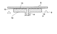
- FIG. 3 is a schematic cross-sectional view for explaining the relationship between a spin chuck stage and a substrate, and shows a state where the substrate is placed on the spin chuck stage.
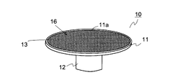
- 1 is a perspective view conceptually showing a substrate stage (spin chuck stage) according to a first embodiment of the present invention.
- the schematic diagram for demonstrating the effect acquired by the substrate stage (spin chuck stage) which concerns on 1st Embodiment of this invention The graph which shows the effect acquired by the substrate stage (spin chuck stage) concerning a 1st embodiment of the present invention.
- Schematic plan view when a substrate stage (spin chuck stage) according to a second embodiment of the present invention is viewed from above
- Schematic plan view when a substrate stage (spin chuck stage) according to a third embodiment of the present invention is viewed from above
- the substrate processing apparatus is a coating apparatus that applies a solution to a substrate
- the substrate processing apparatus is not limited to the coating apparatus, and may be, for example, a developing apparatus for performing a developing process.
- the embodiment shown here is merely an example, and the configuration of the embodiment may be appropriately changed within the scope of the technical idea of the present invention.
- FIG. 1 is a schematic view showing a configuration of a substrate processing apparatus (coating apparatus 1) according to the first embodiment of the present invention.
- a coating apparatus 1 shown in FIG. 1 is used to apply a photoresist solution (form a resist film) to, for example, a semiconductor substrate or a glass substrate for a liquid crystal display.
- a substrate S that is not an element constituting the coating apparatus 1 is also shown for easy understanding.
- the coating apparatus 1 includes a cup 2 having an upper opening.
- a discharge port 2 a is provided at the lower portion of the cup 2.
- a spin chuck stage 10 for adsorbing and rotating the substrate S is disposed in the cup 2.
- the spin chuck stage 10 is connected to the motor 5 via the rotary shaft 4, thereby enabling the spin chuck stage 10 to rotate.
- a nozzle 6 for dropping a photoresist solution onto the substrate S adsorbed on the stage 10 is disposed.
- the coating apparatus 1 includes a rotor cup 3a (rotary body) and a rotor chamber 3b (lid body), and a combination of the two can form a state close to sealing. It has become.
- the rotor cup 3a and the rotor chamber 3b are provided to rotate at the same speed as the spin chuck stage 10.
- the spin chuck stage 10 is an example of the substrate stage of the present invention. Moreover, the motor 5 is an example of the rotating part of the present invention.
- the material constituting the spin chuck stage 10 is not particularly limited, but for example, a resin such as PPS (polyphenylene sulfide) resin, polyimide resin, or fluorine resin is preferable. By configuring the spin chuck stage 10 with resin, the possibility of damaging a glass substrate or the like placed on the stage can be reduced.
- FIG. 2 is a schematic plan view when the substrate stage (spin chuck stage 10) according to the first embodiment of the present invention is viewed from above.
- the spin chuck stage 10 includes a disk-shaped mounting portion 11 on which the substrate S is mounted, and an outer cylindrical column-shaped column portion 12 into which the rotating shaft 4 is fitted. As a whole, it is substantially T-shaped in a side view (sectional view).
- the spin chuck stage 10 provided in a substantially T shape in a side view is connected to the rotary shaft 4 so that the mounting surface 13 (upper surface) on which the substrate S is mounted is horizontal. This is to prevent unevenness in the thickness of the resist film formed on the substrate S.
- a through-hole 14 is formed in the central portion of the spin chuck stage 10 so as to penetrate in the vertical direction (expression considering FIG. 1).
- the through-hole 14 provided in a substantially circular shape when viewed from above has a diameter on the lower side larger than that on the upper side so that the rotary shaft 4 can be fitted and fixed.
- a suction groove 15 (an example of the suction groove of the present invention) for vacuum-sucking the substrate S is formed on the mounting surface 13.
- the suction groove 15 (whose width is about 1 mm, for example) is provided so that the substrate S does not peel from the placement surface 13 due to high-speed rotation.
- the suction groove 15 includes a plurality of annular grooves 15 a formed concentrically around the through hole 14 and a cross-shaped groove 15 b provided so as to intersect at the position of the through hole 14. Each annular groove 15a intersects the cross-shaped groove 15b at four locations. In the state where the substrate S is placed on the placement surface 13, the through hole 14 and the suction groove 15 are provided so as to communicate with each other.
- a through hole 7 is formed inside the rotary shaft 4 so that the suction groove 15 can be decompressed by the decompression unit 8.
- the decompression unit 8 is an example of the decompression unit of the present invention, and a specific example is a vacuum pump.
- a pipe is formed between the vacuum pump and the through hole 7 and an on-off valve that can open and close the communication between the vacuum pump and the through hole 7 is provided.
- FIG. 3A is a schematic cross-sectional view for explaining the relationship between the spin chuck stage 10 and the substrate S, and shows a state before the substrate S is placed on the spin chuck stage 10.
- FIG. 3B is a schematic cross-sectional view for explaining the relationship between the spin chuck stage 10 and the substrate S, and shows a state where the substrate S is placed on the spin chuck stage 10.
- the substrate S is placed on the placement surface 13 of the spin chuck stage 10. Specifically, the substrate S is carried on the spin chuck stage 10 by the transfer arm 9. Then, the spin chuck stage 10 is raised (moved in the direction of arrow U; see FIG. 3A) by an unillustrated lifting mechanism, whereby the substrate S is transferred from the transfer arm 9 to the spin chuck stage 10.
- the present invention is not limited thereto, and in some cases, a configuration in which the substrate S is transferred from the transfer arm 9 to the spin chuck stage 10 by lowering the transfer arm 9 may be adopted.
- the decompression unit 8 When the substrate S is placed on the placement surface 13, the decompression unit 8 is driven and the air in the suction groove 15 is sucked. Thereby, the substrate S is vacuum-sucked on the placement surface 13.
- the spin chuck stage 10 is rotated together with the rotating shaft 4 by driving the motor 5. Before and after this, an appropriate amount of a photoresist solution is dropped from the nozzle 6 onto the substrate S. Further, before the spin chuck stage 10 rotates at high speed, a state close to sealing is formed by the rotor cup 3a and the rotor chamber 3b. As the substrate S rotates, the excess photoresist solution is scattered by the centrifugal force, and the photoresist solution is uniformly applied onto the substrate S. The surplus photoresist solution that has been scattered is discharged out of the cup 2 through the discharge port 2a.
- the driving of the motor 5 and the decompression unit 8 is stopped, and the substrate S placed on the placement surface 13 is transferred to the transfer arm 9.
- the spin chuck stage 10 is lowered (moved in the direction of arrow D; see FIG. 3B) by an elevator mechanism (not shown), whereby the substrate S is moved to the spin chuck stage 10.
- an elevator mechanism not shown
- the substrate S is moved to the spin chuck stage 10.
- a configuration in which the substrate S is transferred from the spin chuck stage 10 to the transfer arm 9 by raising the transfer arm 9 may be adopted.
- the spin chuck stage 10 of the present embodiment is devised so that the charge (charge amount) generated on the substrate S due to peeling charging is minimized. This will be described below.
- FIG. 4 is a perspective view conceptually showing the substrate stage (spin chuck stage 10) according to the first embodiment of the present invention.
- the through hole 14 and the suction groove 15 provided on the mounting surface 13 of the spin chuck stage 10 are omitted.
- the mounting surface 13 of the spin chuck stage 10 is subjected to a roughening process over substantially the entire area.
- the outer periphery (outermost periphery) of the mounting surface 13 is provided with a region 11a (annular region) that has not been subjected to roughening treatment for the purpose of preventing leakage.
- channel 15 is formed may be included in the range where a roughening process is performed, you may make it not include depending on the case.
- the surface roughening treatment method is not particularly limited, and for example, blasting is used.
- the region 11a that is not subjected to the roughening treatment is provided on the outer periphery of the mounting surface 13, and this can be obtained by performing masking during blasting.
- a technique such as etching may be used. By blasting, a lot of fine irregularities (irregularities having a smaller gap than the gap between the mounting surface 13 and the bottom surface of the suction groove 15) are randomly provided on the mounting surface 13 that is originally provided flat (smooth). Can be formed.
- alumina ceramic an example of an abrasive
- Ra arithmetic mean roughness
- FIG. 5 is a schematic diagram for explaining an effect obtained by the substrate stage (spin chuck stage 10) according to the first embodiment of the present invention.
- FIG. 5 shows a partial cross section of the mounting portion 11 (see FIG. 1) constituting the spin chuck stage 10.
- the upper stage (a diagram showing the configuration of the present embodiment) is a diagram showing a state where blasting is performed
- the lower stage is a diagram showing a state where blasting is not performed.
- fine irregularities 16 are formed on the mounting surface 13 that has been subjected to blasting.
- substrate S becomes small in the mounting surface 13 in which the blasting was performed compared with the mounting surface (it corresponds to the conventional structure) in which the blasting is not performed.
- the charge amount of the substrate S generated by peeling the substrate S from the mounting surface 13 can be reduced.
- the unevenness 16 formed on the mounting surface 13 is minute so that the roughness of the mounting surface 13 does not become too large.
- the roughness (Ra) is preferably 0.6 ⁇ m or more and 1.4 ⁇ m or less, and more preferably 0.6 ⁇ m, in order to achieve both reduction of the charge amount and holding of the substrate S when the substrate S is rotated at high speed. More preferably, it is 1.0 ⁇ m or less.
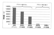
- FIG. 6 is a graph showing effects obtained by the substrate stage (spin chuck stage 10) according to the first embodiment of the present invention.
- FIG. 6 shows the result of measuring the charge amount on the substrate S peeled from the spin chuck stage 10.
- “with blasting” corresponds to the configuration of the present invention (this embodiment), and “without blasting” is a comparative example.
- FIG. 6 it has been demonstrated that the amount of charge on the substrate after peeling from the spin chuck stage can be greatly reduced by blasting the spin chuck stage. From the results shown in FIG. 6, it can be seen that when the PPS resin is used for the spin chuck stage 10, the conductive type is slightly more advantageous than the insulating type.
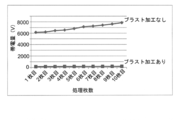
- FIG. 7 is another graph showing the effect obtained by the substrate stage (spin chuck stage 10) according to the embodiment of the present invention.
- FIG. 7 shows the results of examining the change in the charge amount of the substrate S accompanying the change in the number of processed sheets.
- the charge amount is the charge amount of the substrate S after being peeled off from the spin chuck stage 10, and is an actual measurement value.
- “with blasting” corresponds to the configuration of the present invention (this embodiment), and “without blasting” is a comparative example.
- the material of the spin chuck stage 10 is a conductive PPS resin in both cases of “with blasting” and “without blasting”. From the results shown in FIG. 7, it can be seen that by performing blasting on the mounting surface 13, the charge amount of the substrate S can be stably kept low even when the number of processed sheets is increased.
- the spin chuck stage 10 of this embodiment As can be seen from the above, if the spin chuck stage 10 of this embodiment is used, the charge amount of the substrate S peeled off from the spin chuck stage 10 after the photoresist liquid is applied can be suppressed to a low level. In other words, if the spin chuck stage 10 of the present embodiment is used, it is possible to reduce the possibility that an element (TFT or the like) formed on the substrate S is electrostatically damaged, for example. Further, the spin chuck stage 10 of the present embodiment does not need to form an alumina film on the surface thereof, has a simple shape, and is advantageous in terms of manufacturing cost. Second Embodiment
- the substrate processing apparatus coating apparatus
- the substrate stage spin chuck stage
- the configuration of the second embodiment is substantially the same as the configuration of the first embodiment.
- different parts will be described below.
- symbol is attached
- the fine irregularities 16 are formed over substantially the entire area of the mounting surface 13 of the spin chuck stage 10.
- the fine irregularities 16 are formed only in a partial region of the mounting surface 13 of the spin chuck stage 10. More specifically, the region where the fine unevenness 16 is provided is within a plurality of annular regions formed on the mounting surface 13 at intervals (for example, 10 to 30 mm) concentrically (the center being the through hole 14). It has become.
- the fine irregularities 16 are provided in a plurality of annular regions provided along the annular groove 15a (adsorption groove).
- channel 15 is formed may be included in the area
- a region 11a (annular region) that is not subjected to a roughening process for the purpose of preventing leakage is provided on the outer periphery of the mounting surface 13.
- FIG. 8 is a schematic plan view of the substrate stage (spin chuck stage 10) according to the second embodiment of the present invention as viewed from above. Also in the second embodiment, the fine irregularities 16 are obtained by blasting, for example, but in the case of the second embodiment, a mask is arranged on the region where the fine irregularities 16 are not formed and blasting is performed. Will do.
- the frictional force that the substrate S receives from the placement surface 13 is increased as compared with the configuration of the first embodiment. For this reason, when the spin chuck stage 10 is rotated at a high speed (for example, 1500 rpm), the possibility that the substrate S is detached from the spin chuck stage 10 can be reduced. Even in this configuration, since the contact area between the mounting surface 13 and the substrate S is reduced due to the presence of the fine irregularities 16, the substrate S is charged by peeling the substrate S from the mounting surface 13. The amount to be charged (charge amount) can be reduced as compared with the conventional case (a configuration in which no roughening treatment is performed).
- region of the mounting surface 13 is not limited to the structure of 2nd Embodiment, The structure may be changed suitably. However, if the area where the fine unevenness 16 is provided becomes too small, the effect of reducing the amount of charge (charge amount) of the substrate S by peeling the substrate S from the mounting surface 13 becomes small. For this reason, when adopting a configuration in which the fine unevenness 16 is provided only in a partial region of the placement surface 13, this point needs to be considered. When adopting a configuration in which the fine unevenness 16 is provided only in a partial region of the placement surface 13, for example, the fine unevenness 16 is configured to occupy about 1/3 to 1/2 of the placement surface 13. Is preferred.
- a substrate processing apparatus coating apparatus
- a substrate stage spin chuck stage
- the configuration of the third embodiment is substantially the same as the configuration of the first embodiment.
- different parts will be described below.
- symbol is attached
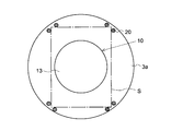
- FIG. 9 is a schematic plan view when the substrate stage (spin chuck stage 10) according to the third embodiment of the present invention is viewed from above.
- FIG. 9 shows not only the substrate stage (spin chuck stage 10) but also the rotor cup 3a. In FIG. 9, the substrate S is also shown for easy understanding.
- the spin chuck stage 10 of the third embodiment is also configured to include a placement unit 11 and a column unit 12.
- a plurality (eight in this embodiment) of lateral shift prevention pins 20 are provided on the rotor cup 3a.
- the lateral shift prevention pin 20 can be a columnar protrusion (pin) extending in the vertical direction (the direction perpendicular to the paper surface in FIG. 9 corresponds). More specifically, the lateral displacement prevention pins 20 are sandwiched between two lateral displacement prevention pins 20 at each of the four corners of the rectangular substrate S when the substrate S is placed on the placement surface 13 of the spin chuck stage 10. It arrange
- the lateral displacement of the substrate S is prevented by the lateral displacement prevention pin 20 that contacts the substrate S even if the substrate S attempts to laterally deviate from the spin chuck stage 10. Is done. For this reason, although the fine unevenness
- the lateral slip prevention pin 21 is an example of the lateral slip prevention part of the present invention.
- shift prevention part is comprised by the mechanical pin 21, the scope of the present invention is not limited to this.
- the lateral shift prevention portion may be, for example, a protruding portion that is provided so as to abut on each of the four corners of the substrate S and is substantially L-shaped in cross section.
- the lateral slip prevention unit may be provided on the spin chuck stage 10 by devising the shape of the spin chuck stage 10.
- the fine irregularities 16 may be provided in substantially the entire area of the placement surface 13 as in the first embodiment, or may be provided on a part of the placement surface 13 as in the second embodiment. May be provided only.
Landscapes
- Container, Conveyance, Adherence, Positioning, Of Wafer (AREA)
- Exposure Of Semiconductors, Excluding Electron Or Ion Beam Exposure (AREA)
Abstract
基板ステージ10は、基板Sが載置される載置面13と、載置面13に設けられて、基板Sを吸着するための吸着溝15と、載置面13の少なくとも一部にランダムに多数設けられる微細な凹凸16と、を備える。
Description
本発明は、基板が載置される基板ステージ、及び、それを備えた基板処理装置に関する。
近年、例えば半導体基板や液晶ディスプレイ用のガラス基板等に回路パターンを形成する場合、フォトリソグラフィー技術が用いられるのが一般的である。フォトリソグラフィー技術によって基板に回路パターンを形成する場合、基板にフォトレジスト液を塗布してレジスト膜を形成し、所定の回路パターンとなるようにレジスト膜を露光後、現像処理するという工程が実行される。
例えば、フォトレジスト液の塗布や現像といった基板処理を行う場合において、基板はスピンチャックステージと呼ばれる回転可能な基板ステージ上に、真空吸着された状態で載置される。フォトレジスト液を塗布して基板を回転させると、基板が摩擦帯電する。また、基板処理後にスピンチャックステージから基板を剥離すると、基板が剥離帯電する。このようにして基板に帯電した電荷は、基板表面に形成された素子(例えば薄膜トランジスター等)を静電破壊する原因となるために問題となる。
上述した静電破壊に対する対策が、例えば特許文献1や特許文献2に開示される。特許文献1には、イオナイザーによって生成されるイオンを利用して、塗布膜を形成する処理の際に帯電した基板の除電を行う構成が開示される。なお、この構成では、イオナイザーによって発生したイオンの基板への搬送は、送風機構によって形成される気流が利用される。
特許文献2には、基板ステージにおける基板の載置面に、所定のエンボス形状を形成した上で、陽極酸化処理によってアモルファス状態のアルミナ皮膜を形成する構成が開示されている。この構成では、アモルファス状態のアルミナ皮膜が緻密かつ強固であるために、剥離帯電防止用の皮膜として機能するとされている。また、載置面に、アルミナ皮膜を形成することに付随してエンボス形状を形成することで、剥離帯電を防止しつつ、良好な温度分布が得られるとされている。
特許文献1の構成は、静電破壊対策として有効な方法であるが、出願人の研究により、この構成でも静電破壊対策が十分でない場合があることがわかった。
また、特許文献2の構成では、基板ステージの載置面に対して、陽極酸化処理(アルミナ皮膜の形成)及びエンボス加工を行う必要があり、基板ステージの構成が複雑で製造に要する費用が高くなってしまう。
さらに、近年、スマートフォンなどのポータブル端末は、画面の大型化(4型以上)、高精細化(300DPI以上)に向かっており、従来よりも静電破壊の問題が深刻になってきている。この原因として、画面が大型化したためにゲート配線が長くなって、アンテナ効果として静電気放電による電荷の影響を受けやすくなったことが考えられる。また、静電破壊の発生箇所がトランジスタ部であることが多いことから、他の原因として、解像度の増加に伴ってトランジスタ部の数が増えて静電破壊を起こす確率が増えたことが考えられる。
以上の点に鑑みて、本発明の目的は、剥離に伴う基板の帯電を抑制可能であるとともに、単純な構成の基板ステージを提供することである。また、本発明の他の目的は、そのような基板ステージを備え、適切に静電気放電対策が施された基板処理装置を提供することである。
上記目的を達成するために本発明の基板ステージは、基板が載置される載置面と、前記載置面に設けられて、前記基板を吸着するための吸着溝と、前記載置面の少なくとも一部にランダムに多数設けられる微細な凹凸と、を備える構成(第1の構成)になっている。
本構成によれば、基板ステージの載置面にランダムに多数の微細な凹凸が設けられる構成になっている。このために、載置面に載置される基板と、基板ステージとの接触面積が低減される。この結果、載置面に載置された基板を載置面から剥離する際に、基板が帯電する量を低く抑制することが可能である。また、本構成の基板ステージは、載置面にアルミナ皮膜を形成する必要がなく、その構造を単純にでき、安価に製造可能である。
上記第1の構成の基板ステージは、回転可能に設けられている構成(第2の構成)であってよい。本構成は、例えば塗布装置等に適用可能である。
上記第1又は第2の構成の基板ステージにおいて、前記載置面の最外周部には微細な凹凸が設けられていない構成(第3の構成)を採用するのが好ましい。本構成によれば、吸着溝を用いて基板を吸着する際にリーク防止を図れる。
上記第1から第3のいずれかの構成の基板ステージにおいて、前記微細な凹凸が設けられている領域のRa(算術平均粗さ)は、0.6μm以上1.0μm以下である構成(第4の構成)が好ましい。本構成によれば、例えば基板ステージが高速回転(例えば1000rpm以上)した場合でも、基板が基板ステージから剥離してしまう可能性を低くできる。
上記第1から第4のいずれかの構成の基板ステージにおいて、前記微細な凹凸が前記載置面の略全域に亘って設けられている構成(第5の構成)であって構わない。本構成によれば、載置面に載置される基板と、基板ステージとの接触面積を極力減らして、基板が載置面から剥離されることによって基板が帯電する量(基板の帯電量)を抑制し易い。
上記第1から第4のいずれかの構成の基板ステージにおいて、前記微細な凹凸が前記載置面の一部の範囲に設けられている構成(第6の構成)であって構わない。本構成において、載置面の一部の範囲は、載置面全域の1/3~1/2程度であるのが好ましい。このように構成することで、基板ステージが高速回転した際に基板が基板ステージから剥離してしまう可能性を低減可能である。
上記第6の構成の基板ステージにおいて、前記一部の範囲は、同心円状に間隔をあけて形成される複数の環状領域を含む構成(第7の構成)であって構わない。
上記第1から第7のいずれかの構成の基板ステージにおいて、前記基板の横ずれを防止する横ずれ防止部を更に備える構成(第8の構成)としてもよい。本構成によれば、基板ステージが高速回転した際に基板が基板ステージから剥離してしまう可能性を低減可能である。
上記第1から第8の構成の基板ステージにおいて、前記微細な凹凸は、ブラスト加工によって形成されている構成(第9の構成)であるのが好ましい。本構成によれば、載置面に多数の凹凸をランダムに得やすい。
また、本発明は上記目的を達成するために、上記第1から第9のいずれかの構成の基板ステージを備える基板処理装置である構成(第10の構成)になっている。本構成の基板処理装置は、適切に静電気放電対策が施されているために、基板処理中に基板表面に形成された素子(例えば薄膜トランジスター等)が静電破壊される可能性が低い。なお、基板処理装置としては、塗布装置や現像装置等が挙げられる。
上記第10の構成の基板処理装置は、前記基板ステージを回転させる回転部と、前記吸着溝を減圧する減圧部と、を更に備える構成(第11の構成)であって構わない。
本発明によると、剥離に伴う基板の帯電を抑制可能であるとともに、単純な構成の基板ステージを提供できる。また、本発明によると、そのような基板ステージを備え、適切に静電気放電対策が施された基板処理装置を提供できる。
以下、本発明の基板ステージ及び基板処理装置の実施形態について、図面を参照しながら詳細に説明する。ここでは、基板処理装置が、基板に溶液を塗布する塗布装置である場合を例に説明する。ただし、基板処理装置は、塗布装置に限定される趣旨ではなく、例えば現像処理を行うための現像装置等であってもよい。また、ここで示す実施形態はあくまでも例示であり、本発明の技術思想の範囲内で、実施形態の構成は適宜変更されても構わない。
<第1実施形態>
<第1実施形態>
まず、本発明の基板ステージが適用された、第1実施形態に係る基板処理装置(塗布装置)の概略構成について説明する。図1は、本発明の第1実施形態に係る基板処理装置(塗布装置1)の構成を示す概略図である。図1に示す塗布装置1は、例えば半導体基板や液晶ディスプレイ用のガラス基板等にフォトレジスト液を塗布する(レジスト膜を形成する)ために使用される。なお、図1においては、理解を容易とするために、塗布装置1を構成する要素ではない基板Sも併せて示されている。
図1に示すように、塗布装置1は、上方が開口したカップ2を備える。このカップ2の下部には、排出口2aが設けられている。カップ2内には、基板Sを吸着して回転するためのスピンチャックステージ10が配置されている。このスピンチャックステージ10は、回転シャフト4を介してモーター5に連結されており、これによりスピンチャックステージ10の回転が可能になっている。また、スピンチャックステージ10の上方には、当該ステージ10に吸着された基板Sにフォトレジスト液を滴下するためのノズル6が配置されている。更に、塗布装置1は、均一な成膜を可能とするために、ローターカップ3a(回転体)とローターチャンバー3b(蓋体)とを備え、この両者の組み合わせによって密封に近い状態を形成できるようになっている。なお、ローターカップ3aとローターチャンバー3bとは、スピンチャックステージ10と同じ速度で回転するように設けられている。
なお、スピンチャックステージ10は、本発明の基板ステージの一例である。また、モーター5は、本発明の回転部の一例である。スピンチャックステージ10を構成する材料としては、特に限定する趣旨ではないが、例えばPPS(ポリフェニレンサルファイド)樹脂、ポリイミド樹脂、フッ素系樹脂等の樹脂が好ましい。樹脂でスピンチャックステージ10を構成することによって、当該ステージ上に載置されるガラス基板等を傷つける可能性を低減できる。
図2は、本発明の第1実施形態に係る基板ステージ(スピンチャックステージ10)を上から見た場合の概略平面図である。図1及び図2にから理解されるようにスピンチャックステージ10は、基板Sが載置される円板状の載置部11と、回転シャフト4が嵌め込まれる外形円柱状の支柱部12とを備え、全体としては側面視(断面視)略T字状になっている。この側面視略T字状に設けられるスピンチャックステージ10は、基板Sが載置される載置面13(上面)が水平となるように回転シャフト4に連結される。これは、基板S上に形成されるレジスト膜の厚みにムラが生じないようにするためである。
また、スピンチャックステージ10の中央部には、上下方向(図1を考慮した表現)に貫通する貫通孔14が形成されている。なお、上面視略円形状に設けられる貫通孔14は、回転シャフト4を嵌め込み固定できるように、上部側に比べて下部側の径が太くなっている。
載置面13には、図2に示すように、基板Sを真空吸着するための吸着溝15(本発明の吸着溝の一例)が形成されている。吸着溝15(その幅は例えば1mm程度)は、高速回転によって基板Sが載置面13から剥離しないように設けられる。吸着溝15は、貫通孔14を中心として同心円状に形成される複数の環状溝15aと、貫通孔14の位置で交差するように設けられる十字状溝15bと、を含む。各環状溝15aは、十字状溝15bと4箇所で交わる。なお、載置面13に基板Sが載置された状態において、貫通孔14と吸着溝15とは連通するように設けられている。
図1に示すように、回転シャフト4の内部には、減圧部8によって吸着溝15を減圧できるように貫通孔7が形成されている。減圧部8は、本発明の減圧部の一例であり、具体例として真空ポンプが挙げられる。なお、真空ポンプと貫通孔7との間には配管が形成され、真空ポンプと貫通孔7との連通を開け閉め可能な開閉弁が設けられる構成とするのが好ましい。
次に、以上のように構成される塗布装置1によって、基板Sにレジスト膜を形成する手順を、図1及び図2に加えて、図3A及び図3Bも参照しながら簡単に説明する。なお、図3Aは、スピンチャックステージ10と基板Sとの関係を説明するための概略断面図で、スピンチャックステージ10に基板Sが載置される前の状態を示す図である。図3Bは、スピンチャックステージ10と基板Sとの関係を説明するための概略断面図で、スピンチャックステージ10に基板Sが載置された状態を示す図である。
まず、基板Sがスピンチャックステージ10の載置面13に載置される。詳細には、基板Sは、搬送アーム9によってスピンチャックステージ10上に運ばれる。そして、スピンチャックステージ10が不図示の昇降機構によって上昇(矢印U方向に移動;図3A参照)されることによって、基板Sは搬送アーム9からスピンチャックステージ10に受け渡される。なお、これに限らず、場合によっては、搬送アーム9が下降することによって基板Sが搬送アーム9からスピンチャックステージ10に受け渡される構成が採用されても構わない。
基板Sが載置面13に載置されると、減圧部8が駆動されて、吸着溝15内の空気が吸引される。これにより、基板Sが載置面13に真空吸着される。次に、モーター5を駆動させることによって、回転シャフト4とともにスピンチャックステージ10を回転させる。これに前後して、ノズル6からフォトレジスト液が基板Sに適量滴下される。また、スピンチャックステージ10の高速回転前に、ローターカップ3aとローターチャンバー3bとによって密封に近い状態が形成される。基板Sの回転に伴い遠心力によって、余剰なフォトレジスト液が飛散され、基板S上には均一にフォトレジスト液が塗布されることになる。なお、飛散された余剰のフォトレジスト液は、排出口2aからカップ2外へと排出される。
フォトレジスト液の塗布が完了すると、モーター5及び減圧部8の駆動が停止され、載置面13に載置された基板Sが搬送アーム9へと受け渡される。詳細には、モーター5及び減圧部8の駆動停止後に、スピンチャックステージ10が不図示の昇降機構によって下降(矢印D方向に移動;図3B参照)されることによって、基板Sはスピンチャックステージ10から搬送アーム9へと受け渡される。なお、場合によっては、搬送アーム9が上昇することによって基板Sがスピンチャックステージ10から搬送アーム9に受け渡される構成が採用されても構わない。
ところで、基板Sが搬送アーム9へと受け渡される際に、基板Sとスピンチャックステージ10との間において剥離帯電が発生する。基板Sに帯電した電荷は、例えば、基板Sの表面に形成された素子を静電破壊する原因となるために、この電荷(帯電量)はできる限り小さなものとするのが好ましい。そして、本実施形態のスピンチャックステージ10は、剥離帯電によって基板Sに生じる電荷(帯電量)が極力小さくなるように工夫されている。以下、これについて説明する。
図4は、本発明の第1実施形態に係る基板ステージ(スピンチャックステージ10)を概念的に示した斜視図である。なお、図4においては、スピンチャックステージ10の載置面13に設けられる貫通孔14や吸着溝15は省略されている。図4に示すように、スピンチャックステージ10の載置面13には、その略全域に亘って粗面化処理が施されている。ただし、載置面13の外周(最外周)には、リーク防止目的で粗面化処理が施されていない領域11a(環状の領域)が設けられている。なお、粗面化処理が行われる範囲には吸着溝15が形成される領域が含まれてよいが、場合によっては含まれないようにしてもよい。
この粗面化処理の手法としては、特に限定されるものではないが、例えばブラスト加工が利用される。上述のように、載置面13の外周には粗面化処理が施されない領域11aが設けられるが、これはブラスト加工の際にマスキングを行うことによって得ることができる。なお、ブラスト加工以外に、例えばエッチング等の手法が利用されてもよい。ブラスト加工によって、元々平ら(滑らか)に設けられる載置面13に、微細な凹凸(載置面13と吸着溝15の底面との間のギャップに比べて小さなギャップを有する凹凸)をランダムに多数形成することができる。平らな表面状態の載置面13に対して、例えばRa(算術平均粗さ)=0.8μm狙いでアルミナセラミック(研磨材の一例)を噴出して材料表面を荒らす。これにより、載置面13に多数の微細な凹凸がランダムに形成されて、例えばRaが0.6~1.0μmの表面状態が得られる。
図5は、本発明の第1実施形態に係る基板ステージ(スピンチャックステージ10)によって得られる効果を説明するための模式図である。図5は、スピンチャックステージ10を構成する載置部11(図1参照)の一部の断面を示すものである。上段(本実施形態を構成を表す図)は、ブラスト加工が施された状態を示す図、下段(比較用図)はブラスト加工が施されていない状態を示す図である。図5に示すように、ブラスト加工が施された載置面13には微細な凹凸16が形成されている。このために、ブラスト加工が施されていない載置面(従来の構成に該当する)に比べて、ブラスト加工が施された載置面13は、基板Sとの接触面積が小さくなる。この結果、載置面13から基板Sを剥離することによって生じる基板Sの帯電量を低減できる。
なお、載置面13のRaが大きくなり過ぎると、スピンチャックステージ10と基板Sとの間に生じる摩擦係数が小さくなり、スピンチャックステージ10を高速回転(例えば1100rpm以上)した時に基板Sを保持できなくなる可能性がある。このために、載置面13に形成される凹凸16は微細なものとして、載置面13の粗度が大きくなり過ぎないようにするのが好ましい。この粗度(Ra)は、帯電量の低減と、基板Sを高速回転させたときの基板Sの保持を両立させるために、0.6μm以上1.4μm以下が好ましく、更には、0.6μm以上1.0μm以下がより好ましい。
図6は、本発明の第1実施形態に係る基板ステージ(スピンチャックステージ10)によって得られる効果を示すグラフである。図6は、スピンチャックステージ10から剥離した基板Sにおける帯電量を測定した結果である。図6において、「ブラスト加工あり」が本発明(本実施形態)の構成に該当し、「ブラスト加工なし」は比較例である。図6において、スピンチャックステージにブラスト加工を施すことによって、スピンチャックステージからの剥離後の基板における帯電量を大きく低減できることが実証されている。なお、図6の結果から、スピンチャックステージ10にPPS樹脂を用いる場合、絶縁性タイプよりも、導電性タイプの方が若干有利であることがわかる。
図7は、本発明の実施形態に係る基板ステージ(スピンチャックステージ10)によって得られる効果を示す別のグラフである。図7は、処理枚数の変化に伴う、基板Sの帯電量変化を調べた結果である。帯電量は、図6の場合と同様に、スピンチャックステージ10から剥離した後の基板Sの帯電量であり、実測値である。図7において「ブラスト加工あり」が本発明(本実施形態)の構成に該当し、「ブラスト加工なし」は比較例である。また、図7において、スピンチャックステージ10の材質は、「ブラスト加工あり」と「ブラスト加工なし」のいずれの場合も、導電性PPS樹脂である。図7に示される結果から、載置面13にブラスト加工を施すことによって、処理枚数が増えた場合でも、安定して基板Sの帯電量を低く保つことができることがわかる。
以上からわかるように、本実施形態のスピンチャックステージ10を用いれば、フォトレジスト液が塗布された後、スピンチャックステージ10から剥離された基板Sの帯電量を低く抑制できる。換言すると本実施形態のスピンチャックステージ10を用いれば、例えば基板S上に形成された素子(TFT等)が静電破壊される可能性を低減できる。また、本実施形態のスピンチャックステージ10は、その表面にアルミナ皮膜の形成を行う必要がなく、その形状が単純で、製造コスト面においても有利である。
<第2実施形態>
<第2実施形態>
次に、第2実施形態の基板処理装置(塗布装置)及び基板ステージ(スピンチャックステージ)について説明する。ただし、第2実施形態の構成は、第1実施形態の構成と概ね同様である。このために、以下、異なる部分について絞って説明する。なお、第1実施形態の構成と重複する部分には同一の符号を付して説明する。
第1実施形態においては、微細な凹凸16が、スピンチャックステージ10の載置面13の略全域に亘って形成された。しかし、第2実施形態では、図8に示すように、微細な凹凸16は、スピンチャックステージ10の載置面13の一部の領域にのみ形成されている。より詳細には、微細な凹凸16が設けられる領域は、載置面13上に同心円状(中心は貫通孔14)に間隔(例えば10~30mm)をあけて形成される複数の環状領域内となっている。換言すると、微細な凹凸16は、環状溝15a(吸着溝)に沿うように設けられる複数の環状領域内に設けられている。なお、微細な凹凸16が設けられる領域には、吸着溝15が形成される領域が含まれてよいが、含まれないようにしてもよい。また、第1実施形態の場合と同様に、載置面13の外周にはリーク防止目的で粗面化処理が施されていない領域11a(環状の領域)が設けられている。
なお、図8は、本発明の第2実施形態に係る基板ステージ(スピンチャックステージ10)を上から見た場合の概略平面図である。また、第2実施形態においても、微細な凹凸16は例えばブラスト加工によって得られるが、第2実施形態の場合には、微細な凹凸16を形成しない領域上にはマスクを配置してブラスト加工を行うことになる。
第2実施形態の構成を採用すると、第1実施形態の構成に比べて基板Sが載置面13から受ける摩擦力が増大する。このために、スピンチャックステージ10を高速回転(例えば1500rpm)する場合に、基板Sがスピンチャックステージ10から離脱する可能性を低減できる。この構成の場合でも、微細な凹凸16の存在によって載置面13と基板Sとの間の接触面積が低減されているために、載置面13から基板Sを剥離することによって基板Sが帯電する量(帯電量)を従来(粗面化処理を全く行わない構成)に比べて低減できる。
なお、微細な凹凸16を載置面13の一部の領域にのみ設ける構成は、第2実施形態の構成に限定されるものではなく、その構成は適宜変更されて構わない。ただし、微細な凹凸16を設ける領域が小さくなりすぎると、載置面13から基板Sを剥離することによって基板Sが帯電する量(帯電量)を低下する効果が小さくなる。このため、微細な凹凸16を載置面13の一部の領域にのみ設ける構成を採用する場合には、この点も考慮する必要がある。微細な凹凸16を載置面13の一部の領域にのみ設ける構成を採用する場合、例えば、微細な凹凸16が載置面13の1/3~1/2程度を占めるように構成するのが好ましい。
<第3実施形態>
次に、第3実施形態の基板処理装置(塗布装置)及び基板ステージ(スピンチャックステージ)について説明する。ただし、第3実施形態の構成は、第1実施形態の構成と概ね同様である。このために、以下、異なる部分について絞って説明する。なお、第1実施形態の構成と重複する部分には同一の符号を付して説明する。
次に、第3実施形態の基板処理装置(塗布装置)及び基板ステージ(スピンチャックステージ)について説明する。ただし、第3実施形態の構成は、第1実施形態の構成と概ね同様である。このために、以下、異なる部分について絞って説明する。なお、第1実施形態の構成と重複する部分には同一の符号を付して説明する。
図9は、本発明の第3実施形態に係る基板ステージ(スピンチャックステージ10)を上から見た場合の概略平面図である。図9には、基板ステージ(スピンチャックステージ10)だけではなく、ローターカップ3aも示されている。また、図9においては、理解を容易とするために基板Sも併せて示されている。
第3実施形態のスピンチャックステージ10も、第1実施形態の場合と同様に、載置部11と、支柱部12とを備える構成である。第3実施形態においては、ローターカップ3a上に複数(本実施形態では8個)の横ずれ防止ピン20が設けられている。横ずれ防止ピン20は、上下方向(図9において紙面と垂直な方向が該当)に延びる円柱状の突出部(ピン)とすることができる。横ずれ防止ピン20は、詳細には、基板Sがスピンチャックステージ10の載置面13に載置された状態において、矩形の基板Sの4つの角部のそれぞれが2つの横ずれ防止ピン20で挟み込まれるように、ローターカップ3a上に配置されている。
このように構成すると、スピンチャックステージ10を高速回転(例えば1500rpm)する場合に、基板Sがスピンチャックステージ10から横ずれしようとしても、基板Sに当接する横ずれ防止ピン20によって基板Sの横ずれは防止される。このため、スピンチャックステージ10の載置面13に微細な凹凸16を設けたにもかかわらず、基板Sが高速回転中にスピンチャックステージ10から離脱する可能性を抑制できる。なお、横ずれ防止ピン20の高さは、基板Sが横ずれしないように適宜調整する必要がある。
なお、横ずれ防止ピン21は、本発明の横ずれ防止部の一例である。また、本実施形態では、横ずれ防止部がメカニカルピン21で構成されているが、本発明の範囲はこれに限定される趣旨ではない。横ずれ防止部は、例えば、基板Sの4つの角部のそれぞれと当接するように設けられる、断面視略L字状に突起部でも構わない。また、場合によっては、横ずれ防止部はスピンチャックステージ10の形状の工夫によってスピンチャックステージ10に設けても構わない。更に第3実施形態において、微細な凹凸16は、第1実施形態のように載置面13の略全域に設けられてもよいし、第2実施形態のように載置面13の一部にのみ設けられてもよい。
1 塗布装置(基板処理装置)
5 モーター(回転部)
8 減圧部
10 スピンチャックステージ(基板ステージ)
13 載置面
15 吸着溝
16 微細な凹凸
21 横ずれ防止ピン(横ずれ防止部)
S 基板
5 モーター(回転部)
8 減圧部
10 スピンチャックステージ(基板ステージ)
13 載置面
15 吸着溝
16 微細な凹凸
21 横ずれ防止ピン(横ずれ防止部)
S 基板
Claims (11)
- 基板が載置される載置面と、
前記載置面に設けられて、前記基板を吸着するための吸着溝と、
前記載置面の少なくとも一部にランダムに多数設けられる微細な凹凸と、
を備えることを特徴とする基板ステージ。 - 当該基板ステージが回転可能に設けられていることを特徴とする請求項1に記載の基板ステージ。
- 前記載置面の最外周部には微細な凹凸が設けられていないことを特徴とする請求項1又は2に記載の基板ステージ。
- 前記微細な凹凸が設けられている領域のRa(算術平均粗さ)は、0.6μm以上1.0μm以下であることを特徴とする請求項1から3のいずれかに記載の基板ステージ。
- 前記微細な凹凸が前記載置面の略全域に亘って設けられていることを特徴とする請求項1から4のいずれかに記載の基板ステージ。
- 前記微細な凹凸が前記載置面の一部の範囲に設けられていることを特徴とする請求項1から4のいずれかに記載の基板ステージ。
- 前記一部の範囲は、同心円状に間隔をあけて形成される複数の環状領域を含む構成であることを特徴とする請求項6に記載の基板ステージ。
- 前記基板の横ずれを防止する横ずれ防止部を更に備えることを特徴とする請求項1から7のいずれかに記載の基板ステージ。
- 前記微細な凹凸は、ブラスト加工によって形成されていることを特徴とする請求項1から8のいずれかに記載の基板ステージ。
- 請求項1から9のいずれかに記載の基板ステージを備えることを特徴とする基板処理装置。
- 前記基板ステージを回転させる回転部と、
前記吸着溝を減圧する減圧部と、
を更に備えることを特徴とする請求項10に記載の基板処理装置。
Priority Applications (2)
| Application Number | Priority Date | Filing Date | Title |
|---|---|---|---|
| CN201380045572.5A CN104603927B (zh) | 2012-08-28 | 2013-08-22 | 基板载置台以及具备其的基板处理装置 |
| JP2014532957A JP5997281B2 (ja) | 2012-08-28 | 2013-08-22 | 基板ステージ及びそれを備えた基板処理装置 |
Applications Claiming Priority (2)
| Application Number | Priority Date | Filing Date | Title |
|---|---|---|---|
| JP2012187765 | 2012-08-28 | ||
| JP2012-187765 | 2012-08-28 |
Publications (1)
| Publication Number | Publication Date |
|---|---|
| WO2014034504A1 true WO2014034504A1 (ja) | 2014-03-06 |
Family
ID=50183319
Family Applications (1)
| Application Number | Title | Priority Date | Filing Date |
|---|---|---|---|
| PCT/JP2013/072344 Ceased WO2014034504A1 (ja) | 2012-08-28 | 2013-08-22 | 基板ステージ及びそれを備えた基板処理装置 |
Country Status (3)
| Country | Link |
|---|---|
| JP (1) | JP5997281B2 (ja) |
| CN (1) | CN104603927B (ja) |
| WO (1) | WO2014034504A1 (ja) |
Cited By (3)
| Publication number | Priority date | Publication date | Assignee | Title |
|---|---|---|---|---|
| JP2016100526A (ja) * | 2014-11-25 | 2016-05-30 | 東京エレクトロン株式会社 | 基板処理装置及び基板処理方法 |
| JPWO2020017314A1 (ja) * | 2018-07-19 | 2020-12-17 | ボンドテック株式会社 | 基板接合装置 |
| JP2023015011A (ja) * | 2021-07-19 | 2023-01-31 | セメス カンパニー,リミテッド | 支持ユニット及びこれを含む基板処理装置 |
Families Citing this family (1)
| Publication number | Priority date | Publication date | Assignee | Title |
|---|---|---|---|---|
| NL2033947B1 (en) * | 2023-01-11 | 2024-07-18 | Suss Microtec Solutions Gmbh & Co Kg | Component for Manufacturing Micro- and/or Nanostructured Devices and Method of Manufacturing the Same |
Citations (4)
| Publication number | Priority date | Publication date | Assignee | Title |
|---|---|---|---|---|
| JPS63287030A (ja) * | 1987-05-20 | 1988-11-24 | Toshiba Corp | ウェハ保持具 |
| JP2004165582A (ja) * | 2002-09-17 | 2004-06-10 | Nikon Corp | 基板ホルダ、基板トレイ、ステージ装置、及び基板ホルダの製造方法 |
| JP2010010719A (ja) * | 2009-10-13 | 2010-01-14 | Tokyo Electron Ltd | 基板処理装置 |
| JP2010161238A (ja) * | 2009-01-08 | 2010-07-22 | Nippon Futsuso Kogyo Kk | フッ素樹脂コーティングプレート及び吸着ステージ |
Family Cites Families (1)
| Publication number | Priority date | Publication date | Assignee | Title |
|---|---|---|---|---|
| TWI439351B (zh) * | 2008-09-29 | 2014-06-01 | 日東電工股份有限公司 | Adsorption tablets |
-
2013
- 2013-08-22 WO PCT/JP2013/072344 patent/WO2014034504A1/ja not_active Ceased
- 2013-08-22 CN CN201380045572.5A patent/CN104603927B/zh not_active Expired - Fee Related
- 2013-08-22 JP JP2014532957A patent/JP5997281B2/ja not_active Expired - Fee Related
Patent Citations (4)
| Publication number | Priority date | Publication date | Assignee | Title |
|---|---|---|---|---|
| JPS63287030A (ja) * | 1987-05-20 | 1988-11-24 | Toshiba Corp | ウェハ保持具 |
| JP2004165582A (ja) * | 2002-09-17 | 2004-06-10 | Nikon Corp | 基板ホルダ、基板トレイ、ステージ装置、及び基板ホルダの製造方法 |
| JP2010161238A (ja) * | 2009-01-08 | 2010-07-22 | Nippon Futsuso Kogyo Kk | フッ素樹脂コーティングプレート及び吸着ステージ |
| JP2010010719A (ja) * | 2009-10-13 | 2010-01-14 | Tokyo Electron Ltd | 基板処理装置 |
Cited By (5)
| Publication number | Priority date | Publication date | Assignee | Title |
|---|---|---|---|---|
| JP2016100526A (ja) * | 2014-11-25 | 2016-05-30 | 東京エレクトロン株式会社 | 基板処理装置及び基板処理方法 |
| JPWO2020017314A1 (ja) * | 2018-07-19 | 2020-12-17 | ボンドテック株式会社 | 基板接合装置 |
| JP2023015011A (ja) * | 2021-07-19 | 2023-01-31 | セメス カンパニー,リミテッド | 支持ユニット及びこれを含む基板処理装置 |
| JP7432664B2 (ja) | 2021-07-19 | 2024-02-16 | セメス カンパニー,リミテッド | 支持ユニット及びこれを含む基板処理装置 |
| US12472596B2 (en) | 2021-07-19 | 2025-11-18 | Semes Co., Ltd. | Support unit and substrate treating apparatus including the same |
Also Published As
| Publication number | Publication date |
|---|---|
| JPWO2014034504A1 (ja) | 2016-08-08 |
| CN104603927A (zh) | 2015-05-06 |
| CN104603927B (zh) | 2016-10-26 |
| JP5997281B2 (ja) | 2016-09-28 |
Similar Documents
| Publication | Publication Date | Title |
|---|---|---|
| JP5997281B2 (ja) | 基板ステージ及びそれを備えた基板処理装置 | |
| JP6139698B2 (ja) | 静電チャック | |
| KR102071727B1 (ko) | 연마 세정 기구, 기판 처리 장치 및 기판 처리 방법 | |
| JP2006310697A (ja) | 吸着チャック | |
| TWI728703B (zh) | 基板處理裝置之轉盤 | |
| JP4570054B2 (ja) | 基板処理装置 | |
| KR20170046083A (ko) | 포토마스크 관련 기판에 이용하는 기판 세정 장치 및 기판 세정 방법 | |
| KR20210095967A (ko) | 자동 클리닝 기능을 갖는 코터 및 코터 자동 클리닝 방법 | |
| JP5795920B2 (ja) | 基板処理装置 | |
| JPWO2012043349A1 (ja) | 吸着プレート | |
| KR100517547B1 (ko) | 포토레지스트 도포 장비 및 이 장비를 사용한포토레지스트 도포 방법 | |
| JP2001343632A (ja) | 液晶表示素子の製造方法 | |
| KR20240093434A (ko) | 반도체 웨이퍼 이송용 로봇암 블레이드에 탈부착되는 이중접합에 의한 미끄럼 방지 패드 | |
| TW202036701A (zh) | 基板處理裝置、基板處理方法以及半導體製造方法 | |
| JPWO2014087761A1 (ja) | 基板処理機構及びこれを用いた小型製造装置 | |
| KR101418301B1 (ko) | 다공질 세라믹 테이블 | |
| TWI646573B (zh) | 聚焦環和電漿處理裝置 | |
| JP4317613B2 (ja) | 基板保持装置 | |
| JP2019140171A (ja) | パターン形成方法及びウェーハの加工方法 | |
| JP2007258467A (ja) | 吸着装置、研磨装置、半導体デバイス製造方法およびこの方法により製造される半導体デバイス | |
| CN103972057A (zh) | 一种半导体精细特征尺寸图形的形成方法 | |
| JP3187310U (ja) | 減圧乾燥処理装置 | |
| KR101043650B1 (ko) | 코팅장비의 코터 척 | |
| JP3881425B2 (ja) | 基板処理装置 | |
| JP2004039978A (ja) | 基板保持装置 |
Legal Events
| Date | Code | Title | Description |
|---|---|---|---|
| 121 | Ep: the epo has been informed by wipo that ep was designated in this application |
Ref document number: 13833750 Country of ref document: EP Kind code of ref document: A1 |
|
| ENP | Entry into the national phase |
Ref document number: 2014532957 Country of ref document: JP Kind code of ref document: A |
|
| NENP | Non-entry into the national phase |
Ref country code: DE |
|
| 122 | Ep: pct application non-entry in european phase |
Ref document number: 13833750 Country of ref document: EP Kind code of ref document: A1 |