WO2014034038A1 - 固体撮像装置 - Google Patents
固体撮像装置 Download PDFInfo
- Publication number
- WO2014034038A1 WO2014034038A1 PCT/JP2013/004857 JP2013004857W WO2014034038A1 WO 2014034038 A1 WO2014034038 A1 WO 2014034038A1 JP 2013004857 W JP2013004857 W JP 2013004857W WO 2014034038 A1 WO2014034038 A1 WO 2014034038A1
- Authority
- WO
- WIPO (PCT)
- Prior art keywords
- inflection point
- pixel
- white reset
- control voltage
- point control
- Prior art date
- Legal status (The legal status is an assumption and is not a legal conclusion. Google has not performed a legal analysis and makes no representation as to the accuracy of the status listed.)
- Ceased
Links
Images







Classifications
-
- H—ELECTRICITY
- H04—ELECTRIC COMMUNICATION TECHNIQUE
- H04N—PICTORIAL COMMUNICATION, e.g. TELEVISION
- H04N25/00—Circuitry of solid-state image sensors [SSIS]; Control thereof
- H04N25/50—Control of the SSIS exposure
- H04N25/57—Control of the dynamic range
Definitions
- the present invention relates to a solid-state imaging device having photoelectric conversion characteristics in which a plurality of photoelectric conversion characteristics are switched at an inflection point.
- CMOS sensor In recent years, in order to expand the dynamic range, a CMOS sensor has been known in which a transfer gate is driven at an intermediate potential in an exposure period, and a linear log characteristic in which a low luminance side has a linear characteristic and a high luminance side has a log characteristic (see, for example, Patent Documents). 1). In such a CMOS sensor, inflection points, which are switching points between linear characteristics and log characteristics, vary from individual to individual.
- Patent Document 2 discloses the following technique. That is, after injecting charges from the floating diffusion into the photodetector, an off voltage higher than the normal off voltage is applied to the transfer transistor for a predetermined waiting time, and the charges are leaked from the photodetector to the floating diffusion. Then, after the standby time has elapsed, the transfer transistor is turned on, the charge accumulated in the photodetector is transferred to the floating diffusion, the output voltage corresponding to the potential of the floating diffusion is read, and the inflection point is read from the read output voltage. It is disclosed that the potential ⁇ 0 is obtained and the potential ⁇ p at the true break point is obtained by adding a certain offset to the potential ⁇ 0.
- An object of the present invention is to provide a solid-state imaging device that can suppress variation between individual inflection points even when imaging conditions change.
- a solid-state imaging device is a solid-state imaging device having a photoelectric conversion characteristic in which a plurality of photoelectric conversion characteristics are switched at an inflection point, and a charge accumulated in the light receiving element, the floating diffusion, and the light receiving element.
- An imaging device including a transfer gate for transferring to the floating diffusion, a white reset process for injecting charges into the light receiving element, and an inflection point control voltage applied to the transfer gate after the white reset process is applied for a predetermined leak period Leak processing, transfer processing for transferring charge remaining in the light receiving element to the floating diffusion after completion of the leak processing, and the imaging device using the potential of the floating diffusion as a white reset signal after completion of the transfer processing.
- White reset signal output processing including read processing An image sensor control unit that performs the white reset signal output processing multiple times by changing the inflection point control voltage and acquires a plurality of white reset signals.
- a white reset characteristic calculation unit that calculates a white reset characteristic indicating a correlation between the white reset signal and the inflection point control voltage based on a plurality of white reset signals acquired by the white reset signal acquisition unit;
- a target value calculation unit that calculates a white reset target value that is a target value of a white reset signal for setting the pixel value of the inflection point to a predetermined target pixel value based on a condition, and the target value calculation unit calculates An inflection point control voltage calculation unit that calculates an inflection point control voltage corresponding to the white reset target value using the white reset characteristic.
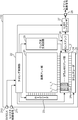
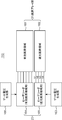
- FIG. 1 is a block diagram showing an overall configuration of a solid-state imaging device according to Embodiment 1 of the present invention. It is a block diagram which shows the detailed structure of the image pick-up element shown in FIG.
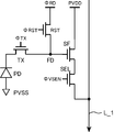
- FIG. 3 is a circuit diagram of pixels constituting the pixel array section shown in FIG. 2. It is a sequence diagram at the time of imaging operation of the circuit shown in FIG. It is a graph which shows the photoelectric conversion characteristic of a certain pixel which comprises an image sensor. It is the graph which showed the difference in the photoelectric conversion characteristic when a shutter speed changes. It is the graph which showed the difference in the photoelectric conversion characteristic when the shutter speed changes, when adjusting the inflection point control voltage so that the pixel value of the inflection point becomes constant.
- the inflection point characteristic which is the relationship between the inflection point control voltage when changing a shutter speed, and the pixel value of an inflection point. It is the graph which showed the difference in the photoelectric conversion characteristic when changing temperature. It is the graph which showed the photoelectric conversion characteristic according to temperature when adjusting the inflection point control voltage so that the pixel value of an inflection point may become constant even if temperature changes. It is the graph which showed the inflection point characteristic when temperature was changed. 6 is a graph showing inflection point characteristics when the shutter speed is set to a certain value and the temperature is set to a certain value. It is the graph which showed the white reset characteristic and the inflection point characteristic.
- FIG. 1 is a block diagram showing an overall configuration of a solid-state imaging device according to Embodiment 1 of the present invention.
- the solid-state imaging device illustrated in FIG. 1 is a solid-state imaging device having a photoelectric conversion characteristic of a linear log characteristic in which a linear characteristic and a log characteristic are switched at an inflection point.
- the solid-state imaging device according to the present embodiment is a solid-state imaging device having a linear log characteristic photoelectric conversion characteristic having a linear characteristic on the low luminance side and a log characteristic on the high luminance side from the inflection point.
- the solid-state imaging device includes an imaging element 110 and an image processing unit 120.
- the image sensor 110 and the image processing unit 120 may be configured in one IC chip or may be configured as separate IC chips.
- the image processing unit 120 includes an image signal processing unit 121 and an image sensor control unit 122.
- the image sensor control unit 122 outputs SYSCLK and the register control signal to the image sensor 110 to control the image sensor 110.
- SYSCLK is a clock signal having a predetermined frequency (for example, 54 MHz) generated by an oscillation circuit (not shown), for example.
- the register control signal is a signal for writing data to various registers included in the timing control unit 22 shown in FIG.
- the image sensor 110 is connected to the image signal processing unit 121 via one channel CH1, and outputs the normal pixel signal D1 and the white reset signal D2 to the image signal processing unit 121 via the channel CH1.
- the normal pixel signal D1 indicates a pixel signal corresponding to the charge accumulated in the light receiving element during the exposure period.
- the white reset signal D2 indicates a pixel signal obtained by executing a white reset signal output process described later.
- the image signal processing unit 121 includes, for example, an image processor, and performs predetermined image processing on the normal pixel signal D1 and the white reset signal D2 output from the image sensor 110.
- the image signal processing unit 121 includes a white reset signal acquisition unit 131, a white reset characteristic calculation unit 132, a target value calculation unit 133, an inflection point control voltage calculation unit 134, a registration unit 135, an inflection point control.
- a voltage setting unit 136 and a calibration table 137 are provided. Details of each block constituting the image signal processing unit 121 will be described later.
- the image sensor control unit 122 controls the image sensor 110 to output the normal pixel signal D1 and the white reset signal D2 from the image sensor. Details of processing of the image sensor control unit 122 will be described later.
- FIG. 2 is a block diagram showing a detailed configuration of the image sensor 110 shown in FIG.
- the image sensor 110 includes a pixel array unit 21, a timing control unit 22, a row decoder 23, a column ADC array unit 24, a column decoder 25, a sense amplifier 26, an LVDS serializer 27, an output terminal 28, a ramp wave generation circuit 29, and an input terminal.
- 210 and 211 are provided.
- the pixel array unit 21 is arranged in a matrix form with M (positive integer) rows ⁇ N (positive integer) columns, and includes a plurality of pixels including light receiving elements.
- the pixel array unit 21 includes light-shielded pixels and normal pixels.
- the normal pixel is mainly used for acquiring the normal pixel signal D1.
- the shading pixel is mainly used for acquiring the white reset signal D2.
- the normal pixel is composed of R, G, and B pixels each including a primary color filter of any of red (R), green (G), and blue (B), for example.
- the R, G, and B pixels are arranged according to a predetermined arrangement pattern such as a Bayer arrangement.
- the light shielding pixel is a pixel in which the light receiving element is shielded from light.
- the timing control unit 22 includes a PLL, a timing generator (TG), and a register, and controls the row decoder 23, the column ADC array unit 24, and the column decoder 25.
- the PLL multiplies (for example, doubles) SYSCLK as necessary and supplies it to the TG.
- the TG generates a timing signal such as a horizontal synchronizing signal and a vertical synchronizing signal in accordance with the signal supplied from the PLL, and supplies the timing signal to the row decoder 23, the column ADC array unit 24, and the column decoder 25 to synchronize their operations. .
- the register holds waveform data for defining the waveforms of various pixel control signals output to each pixel by the row decoder 23, for example.
- the waveform data held by the register is written by a register control signal output from the image sensor control unit 122. Accordingly, each pixel is controlled by the image sensor control unit 122 via the timing control unit 22 and the row decoder 23.
- the row decoder 23 includes, for example, a vertical scanning circuit and a driver circuit.
- the vertical scanning circuit is configured by, for example, a shift register, and cyclically selects each row of the pixel array unit 21 using a vertical synchronization signal output from the timing generator as a trigger, and vertically scans the pixel array unit 21.
- the row decoder 23 may sequentially select the pixel array unit 21 row by row from the upper side to the lower side, or sequentially row by pixel from the lower side to the upper side of the pixel array unit 21. You may choose.
- the driver circuit generates a pixel control signal according to the waveform data written in the register of the timing control unit 22, supplies it to each pixel, and drives each pixel.
- the column ADC array unit 24 includes N column ADCs 24x corresponding to the respective columns of the pixel array unit 21.
- the column ADC 24x is connected to the pixels of each column via the vertical signal line L_1 corresponding to each column of the pixel array unit 21, and reads the pixel signal from the pixels of the row selected by the vertical scanning circuit.
- Each pixel outputs a reference pixel signal that is a pixel signal of a reference component and a reference signal pixel signal that is a pixel signal in which a signal component is superimposed on the reference component in one horizontal period.
- the column ADC 24x includes an AD conversion circuit and a correlated double sampling circuit.
- the AD conversion circuit AD converts each of the reference pixel signal and the reference signal pixel signal.
- the AD conversion circuit counts the time until the level of the ramp signal output from the ramp wave generation circuit 29 exceeds the level of the pixel signal, and the count value is converted into a digital pixel signal.
- the pixel signal is converted into, for example, 14-bit digital data.
- the correlated double sampling circuit obtains a difference between the AD-converted reference pixel signal and the reference signal pixel signal, and generates and holds a signal pixel signal including only the signal component.
- the column decoder 25 is configured by, for example, a shift register, sequentially selects the column ADC 24x of each column in one horizontal period, horizontally scans the column ADC array unit 24, and is a digital signal pixel held by the column ADC 24x of each column. The signals are sequentially output to the sense amplifier 26.
- the sense amplifier 26 amplifies the digital signal pixel signal output from the column ADC array unit 24 via the horizontal signal line L_2 and outputs the amplified signal pixel signal to the LVDS serializer 27.
- the column ADC 24x generates a 14-bit digital signal pixel signal, shifts the phase of each bit signal by 180 degrees, and a signal whose phase is shifted by 180 degrees and a signal whose phase is not shifted. Are output to the sense amplifier 26 in total.
- a total of 28 horizontal signal lines L_2 connecting the column ADC array unit 24 and the sense amplifier 26 are provided.
- the sense amplifier 26 amplifies the signals flowing through the 28 horizontal signal lines L_2, shapes the waveform of each signal, and outputs the waveform to the LVDS serializer 27.
- the LVDS serializer 27 is a serializer conforming to the LVDS (Low Voltage differential signaling) standard.
- the LVDS serializer 27 differentially amplifies a signal output in parallel via the 28 horizontal signal lines L_2 from the sense amplifier 26 and is a 14-bit signal. And converted to serial and output to the output terminal 28.
- the output terminal 28 outputs the signal pixel signal output from the LVDS serializer 27 to the image signal processing unit 121 via the channel CH1.
- the ramp wave generation circuit 29 generates a ramp signal that changes linearly with a certain slope and outputs the ramp signal to each column ADC 24x.
- the input terminal 210 receives SYSCLK supplied from the image sensor control unit 122 and outputs it to the timing control unit 22.
- the input terminal 211 receives a register control signal supplied from the image sensor control unit 122 and outputs the register control signal to the timing control unit 22.
- FIG. 3 is a circuit diagram of pixels constituting the pixel array unit 21 shown in FIG. 3 includes a light receiving element PD (hereinafter referred to as “PD”), a transfer transistor TX (hereinafter referred to as “TX”, an example of a transfer gate), and a reset transistor RST (hereinafter referred to as “RST”).
- PD light receiving element
- TX transfer transistor
- RST reset transistor
- Amplifying transistor SF hereinafter referred to as “SF”
- SEL row selection transistor
- FD floating diffusion FD
- PD is composed of, for example, a buried photodiode, and at reset, RST and TX are turned on, and a negative drive voltage PVSS (hereinafter referred to as “PVSS”) is applied to the anode.
- PVSS negative drive voltage
- TX is composed of, for example, nMOS (negative channel, metal, and oxide semiconductor), and transfers the charge accumulated by the PD to the FD.
- a gate voltage ⁇ TX (an example of a pixel control signal, hereinafter referred to as “ ⁇ TX”) for turning on / off TX is input to the gate terminal of TX.
- the drain of TX is connected to RST via FD.
- ⁇ TX goes to a low level
- Hi high level
- FD accumulates the charge transferred from PD. Thereby, a voltage corresponding to the electric charge appears in the FD.
- RST is composed of, for example, an nMOS, resets the FD, and discharges the charge accumulated in the FD to the outside of the FD.
- a reset signal ⁇ RST (an example of a pixel control signal, hereinafter referred to as “ ⁇ RST”) for turning on / off the RST is input to the gate terminal of the RST, and a charge for injecting charge into the PD is input to the drain.
- a charge injection signal ⁇ RD (an example of a pixel control signal, hereinafter referred to as “ ⁇ RD”) is input.
- PVDD and PVSS are output from a voltage source (not shown), and ⁇ RD and ⁇ RST are output from the row decoder 23.
- SF is composed of, for example, an nMOS
- the gate terminal is connected to TX and RST via FD
- the PVDD is input to the drain terminal
- the source terminal is connected to SEL.
- the SF amplifies the voltage appearing on the FD and outputs it to the SEL.
- SEL is composed of, for example, an nMOS, and a row selection signal ⁇ VSEN (an example of a pixel control signal, hereinafter referred to as “ ⁇ VSEN”) is input to a gate terminal, a drain is connected to SF, and a source is a vertical signal line L_1. To the column ADC 24x of the corresponding row. Then, the SEL outputs the voltage amplified by the SF as a pixel signal to the column ADC 24x of the corresponding column via the vertical signal line L_1.
- ⁇ VSEN is output from the row decoder 23.
- FIG. 4 is a sequence diagram during the imaging operation of the circuit shown in FIG. Note that the sequence diagram shown in FIG. 4 is a sequence common to the light-shielding pixels and the normal pixels. Therefore, although the normal pixel outputs a white reset signal in addition to the normal pixel signal, the white reset signal is not used in the image signal processing unit 121 to calculate the white reset characteristic. In addition to the white reset signal, the light-shielded pixel also outputs a normal pixel signal, but this normal image signal does not represent subject information.
- Period t0 is the exposure period of the previous frame.
- ⁇ RD Hi
- ⁇ RST Hi
- FD is always reset.
- the charge accumulated in the PD cannot exceed the TX potential barrier, and thus has a linear characteristic.
- a part of the charge accumulated in the PD can leak into the FD over the TX potential barrier. Accordingly, since the PD accumulates charges while flowing the charges to the FD, the charges accumulated in the PD have log characteristics. As a result, a linear log characteristic in which the low luminance has a linear characteristic and the high luminance side has a log characteristic is realized.
- the inflection point is controlled by adjusting the value of the intermediate potential Mid.
- the intermediate potential Mid is referred to as “inflection point control voltage”.
- the period t1 is a reading period of the reference pixel signal of the normal pixel signal D1.
- ⁇ RD Hi
- ⁇ RST Lo
- ⁇ VSEN Hi.
- the potential of the FD decreases from PVDD to V_Ref
- the potential V_Ref is read to the column ADC 24x (see FIG. 2) as a reference pixel signal.
- the ramp signal RP_Ref corresponding to the reference pixel signal is input from the ramp wave generation circuit 29 in synchronization with the reading of the reference pixel signal.
- the column ADC 24x AD-converts the reference pixel signal of the normal pixel signal D1.
- the ramp signal RP_Ref has a waveform in which the voltage decreases linearly with a certain slope. Therefore, the column ADC 24x counts the time until the ramp signal RP_Ref reaches the reference pixel signal from the maximum value V_M, and AD converts the reference pixel signal.
- the amplitude A41 of the ramp signal RP_Ref a value slightly larger than the assumed maximum value of the reference pixel signal is employed.
- the period t2 is a charge transfer period from the PD to the FD.
- ⁇ TX Hi, and the charge accumulated in the PD is transferred to the FD.
- the potential of the FD decreases from V_Ref to V_Sig.
- the value of the potential V_Sig has a value corresponding to the amount of charge transferred from the PD to the FD, that is, a value corresponding to the illuminance of the subject.
- the period t3 is a period for reading the reference signal pixel signal of the normal pixel signal D1.
- ⁇ VSEN Hi
- V_Sig of the FD is read to the column ADC 24x as a reference signal pixel signal.
- the ramp signal RP_Sig corresponding to the reference signal pixel signal is input from the ramp wave generation circuit 29 to the column ADC 24x in synchronization with the reading of the reference signal pixel signal.
- the column ADC 24x compares the ramp signal RP_Sig with the reference signal pixel signal, and AD-converts the reference signal pixel signal.
- the column ADC 24x takes a difference between the reference pixel signal obtained in the period t1 and the reference signal pixel signal obtained in the period t3, and generates a signal pixel signal.
- the normal pixel signal D1 is obtained.
- the ramp signal RP_Sig has a waveform in which the voltage linearly decreases from the maximum value V_M with a certain slope. Therefore, the column ADC 24x counts the time until the ramp signal RP_Ref reaches the reference signal pixel signal from the maximum value V_M, and AD-converts the reference signal pixel signal. As the amplitude A42 of the ramp signal RP_Ref, a value slightly larger than the maximum value of the assumed reference signal pixel signal of the normal pixel signal D1 is employed.
- Period t5 is a white reset period.
- ⁇ RD Lo
- ⁇ RST Hi
- reset means emptying the charge of the PD.
- this reset is referred to as a black reset.
- this reset is called a white reset to distinguish it from a black reset.
- Period t6 is a leak period TA after white reset. ⁇ RD is returned to Hi, ⁇ TX is set to Mid, and the charge accumulated in the PD due to the white reset is leaked to the FD, so that the charge of the PD gradually decreases.
- the PD has a charge up to the potential barrier of TX, that is, a charge amount indicating the pixel value of the inflection point of the linear log characteristic.
- TX potential barrier of TX
- the amount of charge remaining in the PD after the end of the leak period TA has a value correlated with the TX potential barrier. . That is, if the leak period TA is secured for a certain period, the amount of charge remaining in the PD is not a value indicating the potential barrier itself, but has a value correlated with the potential barrier. Therefore, by reading out the charge remaining in the PD as a pixel signal from each pixel at the end of the leak period TA, it is possible to specify the variation in the pixel value of the inflection point of each pixel.
- the column ADC 24x receives the ramp signal RP_WRef corresponding to the reference signal of the white reset signal D2, and AD converts the reference signal of the white reset signal D2.
- the amplitude A43 of the ramp signal RP_WRef a value similar to the amplitude A41 may be adopted.
- the column ADC 24x compares the reference signal pixel signal with the ramp signal RP_WSig corresponding to the reference signal pixel signal of the white reset signal D2, and AD-converts the reference signal pixel signal. Then, the column ADC 24x takes the difference between the reference pixel signal obtained in the period t7 and the reference signal pixel signal obtained in the period t9, and generates a signal pixel signal of the white reset signal D2.
- the period t10 is the exposure period of the next frame, and the same processing as the period t1 is performed. Thereafter, the processing shown in the periods t0 to t10 is repeated, and the normal pixel signal D1 and the white reset signal D2 are obtained in one frame period.
- FIG. 5 is a graph showing the photoelectric conversion characteristics G50 of a certain pixel constituting the image sensor 110, where the vertical axis shows the pixel value and the horizontal axis shows the illuminance of the subject in logarithm.
- the photoelectric conversion characteristic G50 has a linear characteristic in a region where the illuminance is equal to or lower than the inflection point P50, and has a log characteristic in a region where the illuminance is equal to or higher than the inflection point P50.
- the linear characteristic draws a curve and the log characteristic draws a straight line because the horizontal axis is a logarithmic axis.
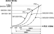
- FIG. 6 is a graph showing the difference in photoelectric conversion characteristics when the shutter speed SS changes, and the vertical axis and the horizontal axis are the same as those in FIG.
- Photoelectric conversion characteristics G61 to G63 are photoelectric conversion characteristics when the shutter speed SS is 1/30, 1/250, and 1/2000, respectively.
- the inflection point control voltage applied to the transfer transistor TX is constant during the exposure period, and the inflection point control voltage is not adjusted. Therefore, it can be seen that the pixel values of the inflection points P61, P62, and P63 become higher as D61 ⁇ D62 ⁇ D63 as the shutter speed SS becomes shorter.
- the pixel values of the inflection points P61, P62, and P63 increase as D61 ⁇ D62 ⁇ D63. Therefore, it can be seen that the dynamic range becomes narrower in the order of DM61> DM62> DM63.
- FIG. 7 is a graph showing the difference in photoelectric conversion characteristics when the shutter speed SS changes when the inflection point control voltage is adjusted so that the pixel value of the inflection point is constant.
- the horizontal axis is the same as in FIG.
- Photoelectric conversion characteristics G71 to G73 are photoelectric conversion characteristics when the shutter speed SS is 1/30, 1/250, and 1/2000, respectively.
- the inflection point control voltage is adjusted so that the pixel values of the inflection points P71, P72, and P72 maintain D70 even when the shutter speed SS changes. Specifically, as the shutter speed is shortened to 1/30, 1/250, and 1/2000, the value of the inflection point control voltage is set higher and the TX potential barrier is lowered.
- the dynamic range DM72 has the same log characteristic range as that of the dynamic range DM71, and the dynamic range is made constant.
- the dynamic range DM 73 has a log characteristic area that is the same as the log characteristic area of the dynamic range DM 71 in the same manner as the dynamic range DM 72, and the dynamic range is constant.
- the dynamic range can be made constant by adjusting the inflection point control voltage so that the pixel value of the inflection point becomes a constant value.
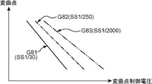
- FIG. 8 is a graph showing an inflection point characteristic that is a relationship between the inflection point control voltage and the inflection point pixel value when the shutter speed SS is changed, and the vertical axis represents the inflection point pixel value.
- the abscissa indicates the inflection point control voltage.
- inflection point characteristics G81 to G83 are inflection point characteristics when the shutter speed SS is 1/30, 1/250, and 1/2000, respectively. As the shutter speed SS is shortened to 1/30, 1/250, and 1/2000, the inflection point characteristics G81, G82, and G83 are shifted to the right. Further, the inflection point characteristics G81, G82, and G83 have a gentler slope and a reduced gain as the shutter speed SS becomes shorter.
- the inflection point control voltage is constant, the pixel value at the inflection point increases as the shutter speed SS decreases, and the photoelectric conversion characteristics G61 to G63 shown in FIG. 6 are inflection point characteristics G81 to G83. It can be seen that is reflected in.
- FIG. 9 is a graph showing the difference in photoelectric conversion characteristics when the temperature is changed, and the vertical axis and the horizontal axis are the same as those in FIG.
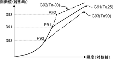
- Photoelectric conversion characteristics G91, G92, and G93 indicate the photoelectric conversion characteristics when the temperatures are Ta25, Ta-30, and Ta90, respectively. However, Ta90> Ta25> Ta-30.
- the temperature refers to the environmental temperature in the pixel array unit 21.
- the pixel value at the inflection point also changes, so that the dynamic range varies greatly.
- FIG. 10 is a graph showing photoelectric conversion characteristics according to temperature when the inflection point control voltage is adjusted so that the pixel value at the inflection point is constant even when the temperature changes. The pixel value is shown, and the horizontal axis shows the illuminance in logarithm.
- photoelectric conversion characteristics G101, G102, and G103 are photoelectric conversion characteristics when the temperatures are Ta25, Ta-30, and Ta90, respectively.
- the pixel values of the inflection point P100 are all constant at D100. Therefore, by adjusting the inflection point control voltage, the sensitivity of the log characteristics cannot be made constant, but the pixel value D100 of the inflection point P100 can be made constant. As a result, the variation of the photoelectric conversion characteristics G101, G102, and G103 becomes only the sensitivity of the log region, and the variation of the dynamic range can be reduced and the dynamic range can be made approximately constant compared to the case of FIG.
- FIG. 11 is a graph showing the inflection point characteristics when the temperature is changed.
- the vertical axis represents the pixel value of the inflection point, and the horizontal axis represents the inflection point control voltage.
- inflection point characteristics G111, G112, and G113 are inflection point characteristics when the temperatures are Ta25, Ta-30, and Ta90, respectively. However, Ta90> Ta25> Ta-30.
- the inflection point characteristics G113, G111, G112 are shifted to the right. It can also be seen that the inflection point characteristics G113, G111, and G112 increase in slope and gain as the temperature decreases.
- the shutter speed SS and the temperature change respectively.
- the inflection point control voltage needs to be determined in consideration of both the inflection point characteristics G111 to G113.
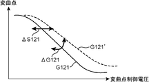
- FIG. 12 is a graph showing the inflection point characteristic G121 when the shutter speed SS is set to a certain value and the temperature is set to a certain value.
- an inflection point characteristic G121 ′ in which the horizontal axis is shifted by the offset error ⁇ S121 with respect to the inflection point characteristic G121 and the gain is shifted by the gain error ⁇ G121 with respect to the inflection point characteristic G121 is obtained. It is done.
- the inflection point characteristics are different for each chip, if the inflection point control voltage is set to the same value between different chips, the pixel value of the inflection point is shifted for each chip. Therefore, in order to align the pixel values of the inflection points in all the chips, it is necessary to measure the inflection point characteristics as shown in FIGS. 8 and 11 for each chip and calibrate in advance before shipment from the factory. There is.
- the solid-state imaging device performs such calibration at the time of imaging operation, not before shipment from the factory. This will be specifically described below.
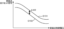
- FIG. 13 is a graph showing the white reset characteristic G131 and the inflection point characteristic G132.
- the vertical axis represents the pixel value of the inflection point or the pixel value of the white reset signal, and the horizontal axis represents the inflection point control voltage. Show.
- the white reset characteristic indicates the relationship between the inflection point control voltage applied to the transfer transistor TX in the leak period TA shown in FIG. 4 and the pixel value of the white reset signal.
- the inflection point characteristics indicate the relationship between the inflection point control voltage and the pixel value of the inflection point.
- FIG. 13 shows the white reset characteristic G131 and the inflection point characteristic G132 under the same imaging conditions, that is, when the temperature and the shutter speed SS are the same.
- the white reset characteristic G131 has a waveform obtained by shifting the inflection point characteristic G132 on the vertical axis by the offset component ⁇ WR, and there is a correlation between the two. I understand.
- the pixel value of the inflection point can be specified by subtracting the offset component ⁇ WR from the pixel value.
- the inflection point characteristic can be obtained by subtracting the offset component ⁇ WR from the white reset characteristic, and the pixel value of the inflection point can be obtained from the inflection point characteristic.
- the target pixel value of the inflection point corresponds to the imaging condition. If the offset component ⁇ WR is added, a white reset target value that is a target value of the white reset signal is obtained. Then, an inflection point control voltage corresponding to the white reset target value is obtained from the white reset characteristic. When the normal pixel is driven with this inflection point control voltage, the pixel value at the inflection point can be made the target pixel value.
- the shutter speed SS and the temperature are adopted as the imaging conditions. Therefore, the offset component ⁇ WR employs a function having two parameters, shutter speed SS and temperature. Since this function has almost no variation among individuals, a function common to all individuals may be stored in the solid-state imaging device in advance.
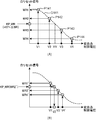
- FIG. 14A and 14B are explanatory diagrams of the calculation principle of the inflection point control voltage for setting the pixel value of the inflection point to the target pixel value, and the vertical axis indicates the pixel value of the white reset signal.
- the horizontal axis indicates the inflection point control voltage.
- FIG. 14A first, the pixel values WR1 to WR4 of the white reset signal for the four points of the voltages V1 to V4 are measured.
- four measurement points P141 to P144 defined by the voltages V1 to V4 and the pixel values WR1 to WR4 are plotted on the graph shown in FIG.
- the measurement points P141 to P144 are interpolated to calculate the white reset characteristic G141.
- linear interpolation that linearly approximates the measurement points P141 to P144 may be employed as the interpolation.
- the white reset characteristic G141 may be obtained by fitting the reference waveform of the white reset characteristic to the measurement points P141 to P144. Thereby, the white reset characteristic G141 is obtained as a function.
- the offset component ⁇ WR of the current imaging condition is added to the target pixel value KP at the inflection point, and the white reset target value KP_WR is calculated.
- the white reset target value KP_WR is substituted into the white reset characteristic G141, and the inflection point control voltage VV is calculated.
- the transfer transistor TX is driven with the inflection point control voltage VV, the pixel value at the inflection point can be set to the target pixel value KP.
- the pixel values WR1 ′ to WR4 ′ of the white reset signal for the voltages V1 ′ to V4 ′ are measured. Thereby, it is checked whether the pixel value WR2 ′ is really the white reset target value KP_WR.
- the voltage V2 ′ is set as the inflection point control voltage.
- the voltages V1 to V4 shown in FIG. 14A are set in regions different from the previous time, and again shown in FIGS. 14A and 14B.
- the inflection point control voltage is calculated by performing the processing described in (1).
- the reason why the pixel value WR2 ′ does not become the white reset target value KP_WR for example, the case where the voltages V1 to V4 are applied to the curved portion of the white reset characteristic G141 shown in FIG. Therefore, in this case, it is preferable to set the voltages V1 to V4 so that the voltages V1 to V4 are applied to the linear portion of the white reset characteristic G141.
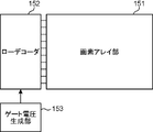
- FIG. 15 is a block diagram showing a configuration of an imaging element 110 of a comparative example of the solid-state imaging device according to the embodiment of the present invention.
- the imaging device of the comparative example includes a pixel array unit 151, a row decoder 152, and a gate voltage generation unit 153.
- the timing control unit 22, the column ADC array unit 24 to the ramp wave generation circuit 29 shown in FIG. 2 are not shown.
- the pixel array unit 151 includes an effective pixel area including effective pixels for acquiring the normal pixel signal D1 and a light-shielding pixel area including light-shielding pixels for measuring a black level reference value and the like.
- the gate voltage generation unit 153 supplies the gate voltage ⁇ TX including the inflection point control voltage to the pixel array unit 151 via the row decoder 152.
- the image sensor 110 employs the following configuration.
- FIG. 16 is a block diagram showing a configuration of the imaging element 110 of the solid-state imaging device according to the embodiment of the present invention.
- the image sensor 110 in addition to the pixel array unit 21 and the row decoder 23 illustrated in FIG. 2, the image sensor 110 further includes a gate voltage generation unit 166 (an example of a first voltage generation unit), and a gate voltage generation unit. 163 (an example of a second voltage generation unit).
- the timing control unit 22, the column ADC array unit 24 to the ramp wave generation circuit 29 shown in FIG. 2 are not shown.
- the pixel array unit 21 includes an effective pixel region 161 and a light shielding pixel region 162.
- effective pixels including PDs that are not shielded from light are arranged in a matrix of predetermined rows ⁇ predetermined columns.
- light-shielded pixels including PDs that are shielded from light in a predetermined row ⁇ predetermined column are arranged in a matrix in a predetermined row ⁇ predetermined column.
- the number of rows in the light-shielding pixel region 162 the number of rows corresponding to the type of calibration transfer control voltage may be adopted.
- four types of voltages V1 to V4 are employed as calibration transfer control voltages. Therefore, the number of rows of the light-shielding pixel region 162 is four.
- the row decoder 23 includes a row decoder 164 and a row decoder 165.
- the row decoder 164 is a row decoder for the effective pixel region 161 and supplies the gate voltage ⁇ TX generated by the gate voltage generation unit 166 to each row of the effective pixel region 161.
- the row decoder 165 is a row decoder for the light-shielded pixel region 162, and supplies the gate voltage ⁇ TX generated by the gate voltage generation unit 166 to each row of the light-shielded pixel region 162.
- the gate voltage generation unit 166 generates a gate voltage ⁇ TX to be applied to the effective pixel, and supplies it to the transfer transistor TX of each effective pixel constituting the effective pixel region 161 via the row decoder 164.
- the gate voltage ⁇ TX includes Hi, Lo, and Mid (inflection point control voltage) as shown in FIG. 4, the gate voltage generation unit 166 generates these voltages.
- the gate voltage generation unit 163 generates a gate voltage ⁇ TX that is a gate voltage ⁇ TX to be applied to the light-shielded pixels and obtains the white reset characteristics, and each light-shielded pixel that configures the light-shielded pixel region 162 via the row decoder 165. To the transfer transistor TX.
- the gate voltage generation unit 163 since the gate voltage ⁇ TX for obtaining the white reset characteristic also has Hi, Lo, Mid (inflection point control voltage), the gate voltage generation unit 163 generates these voltages.
- the gate voltage generation unit 163 generates four types of gate voltages ⁇ TX having inflection point control voltages V1 to V4 and supplies them to the row decoder 165.
- the row decoder 165 supplies a gate voltage ⁇ TX having inflection point control voltages V1 to V4 to the first to fourth rows of light shielding pixels in the light shielding pixel region 162, respectively.
- the effective pixel can perform an imaging operation, and the four types of gate voltages ⁇ TX can be supplied to the light-shielding pixel to measure the white reset signal.
- the image sensor control unit 122 performs white reset signal output processing on the light-shielded pixels.
- the white reset signal output process includes a white reset process, a leak process, a transfer process, and a read process.
- the white reset process is executed in the period t5 in FIG. 4 and is a process for injecting charges into the PD and filling up the charge amount accumulated in the PD.
- the leak process is executed in the period t5 in FIG. 4, and after the white reset process is completed, the inflection point control voltage is applied to the transfer transistor TX for a predetermined leak period TA.
- the transfer process is a process that is executed in the period t8 of FIG. 4 and transfers the charge remaining in the PD to the FD after the end of the leak process.
- the white reset signal output process is executed in the period t9 in FIG. 4, and after the transfer process is completed, the FD potential is read from the light-shielded pixel as a white reset signal.
- the image sensor control unit 122 causes both the effective pixel and the light-shielded pixel to execute the processing shown in the period t0 to t9 in FIG. 4 in one frame period. Therefore, in FIG. 4, an inflection point control voltage for imaging is adopted as the Mid for the effective pixel. Also, the inflection point control voltage of V1 is adopted as Mid for the light shielding pixels in the first row shown in FIG. 16, and the inflection point control voltage of V2 is adopted as Mid for the light shielding pixels in the second row. The inflection point control voltage of V3 is adopted as Mid for the light shielding pixel of the eye, and the inflection point control voltage of V4 is adopted as Mid for the light shielding pixel of the fourth row.
- the white reset signal acquisition unit 131 illustrated in FIG. 1 causes the image sensor control unit 122 to execute the white reset signal output processing a plurality of times while changing the inflection point control voltage to acquire a plurality of white reset signals.
- the signal output process is executed multiple times.
- the white reset signal acquisition unit 131 acquires the pixel values WR1 to WR4 of the white reset signal from the light-shielded pixels in the first to fourth rows.
- the white reset characteristic calculation unit 132 calculates a white reset characteristic indicating a correlation between the white reset signal and the inflection point control voltage based on the plurality of white reset signals acquired by the white reset signal acquisition unit 131.
- the white reset characteristic calculator 132 calculates the white reset characteristic using the pixel values WR1 to WR4 of the white reset signal.
- the white reset characteristic calculation unit 132 calculates the average value of the pixel values of the white reset signal in each column of the first to fourth rows of the light-shielded pixel region 162 as the pixel values WR1 to WR4, and calculates one white reset characteristic. do it.
- the target value calculation unit 133 sets a white reset target value KP_WR that is a target value of a white reset signal for setting the pixel value of the inflection point to a predetermined target pixel value KP based on the current imaging conditions of the solid-state imaging device. calculate. Specifically, the target value calculation unit 133 holds in advance a function for specifying the offset component ⁇ WR using the temperature and the shutter speed SS as parameters, and using this function, the offset component ⁇ WR corresponding to the current imaging condition. Ask for. Then, the target value calculation unit 133 calculates the white reset target value KP_WR by adding the offset component ⁇ WR to the target pixel value KP.
- the inflection point control voltage calculation unit 134 calculates the inflection point control voltage VV corresponding to the white reset target value KP_WR calculated by the target value calculation unit 133 using the white reset characteristic.
- the registration unit 135 registers the inflection point control voltage VV calculated by the inflection point control voltage calculation unit 134 in the calibration table 137 in association with the imaging condition.
- the inflection point control voltage setting unit 136 identifies an inflection point control voltage corresponding to the current imaging condition from the calibration table 137, and a gate voltage generation unit that generates the gate voltage ⁇ TX having the identified inflection point control voltage as Mid. 166 to generate. If the inflection point control voltage corresponding to the current imaging condition is not registered in the calibration table 137, the inflection point control voltage setting unit 136 uses the inflection point control voltage registered in the calibration table 137. A corresponding inflection point control voltage may be calculated by interpolation.
- the inflection point control voltage setting unit 136 has, for example, the inflection point control voltage obtained in the previous frame until the number of inflection point control voltages registered in the calibration table 137 reaches a predetermined number.
- the gate voltage generation unit 166 may generate the gate voltage ⁇ TX.
- the calibration table 137 is a table in which the imaging conditions and the inflection point control voltage are associated with each other, and the inflection point control voltage is registered by the inflection point control voltage calculation unit 134 as needed.
- the calibration table 137 is stored in, for example, a rewritable nonvolatile memory.
- FIG. 17 is a flowchart showing calibration of the inflection point control voltage according to the embodiment of the present invention.
- the target value calculation unit 133 specifies an offset component ⁇ WR corresponding to an imaging condition defined by a certain shutter speed SS and temperature (S171).
- the shutter speed SS may be set by the image sensor control unit 122 based on, for example, an operation instruction from the user or the illuminance of the subject. What is necessary is just to employ
- the target value calculation unit 133 calculates the white reset target value KP_WR by adding the offset component ⁇ WR to the target pixel value KP at the inflection point (S172).
- the white reset signal acquisition unit 131 sets inflection point control voltages of voltages V1 to V4 in order to acquire white reset characteristics (S173).
- the gate voltage ⁇ TX having voltages V1 to V4 as Mid is applied to the light-shielding pixels in the first to fourth rows, and the variable currently set as Mid is applied to the effective pixels.
- a gate voltage ⁇ TX having a curvature control voltage VV is applied.
- the white reset signal acquisition unit 131 reads the pixel values WR1 to WR4 of the white reset signal for the voltages V1 to V4 from the light-shielded pixels in the first to fourth rows (S174).
- the white reset characteristic calculation unit 132 calculates the white reset characteristic from the pixel values WR1 to WR4 of the white reset signal (S175).
- the inflection point control voltage calculation unit 134 substitutes the white reset target value KP_WR calculated in S172 for the function indicating the white reset characteristic calculated in S175, and the inflection corresponding to the white reset target value KP_WR.
- the point control voltage VV is calculated (S176).
- the white reset signal acquisition unit 131 sets the voltages V1 ′ to V4 ′ so that the interval is narrower than the voltages V1 to V2 set in S173 and the inflection point control voltage becomes the voltage V2 ′ ( S177).
- the gate voltage ⁇ TX having voltages V1 ′ to V4 ′ as Mid is applied to the light-shielding pixels in the first to fourth rows, and the effective pixel is currently set as Mid.
- a gate voltage ⁇ TX having an inflection point control voltage VV is applied. Note that S177 is executed in the next frame after S173.
- the white reset signal acquisition unit 131 reads the pixel values WR1 ′ to WR4 ′ of the white reset signal for the voltages V1 ′ to V4 ′ from the light-shielded pixels in the first to fourth rows (S178).
- the inflection point control voltage calculation unit 134 determines whether or not the pixel value WR2 ′ of the white reset signal is the white reset target value KP_WR (S179). If the pixel value WR2 ′ is not equal to the white reset target value KP_WR (NO in S179), the process returns to S173. Then, the white reset signal acquisition unit 131 sets the voltages V1 to V4 in a region different from the previously set voltages V1 to V4 (S173), and the processes after S174 are executed. Note that S173 is executed in the next frame after S177.
- the registration unit 135 sets the voltage V2 ′ set in S177 as the inflection point control voltage VV and corresponds to the corresponding imaging condition. At the same time, it is registered in the calibration table 137 (S180), and the process returns to S171.
- the offset component ⁇ WR corresponding to the imaging condition is specified, and the processes after S172 are executed.
- the pixel values WR1 to WR4 of the white reset signal with respect to the voltages V1 to V4 are acquired, and the white reset characteristics are obtained from the acquired pixel values WR1 to WR4.
- the white reset target value NP_WR is calculated by adding the offset component ⁇ WR corresponding to the imaging condition to the target pixel value NP at the inflection point.
- the inflection point control voltage VV corresponding to the white reset target value NP_WR is calculated from the white reset characteristic.
- the individual inflection point control voltage VV according to the imaging conditions can be specified, and variations between the inflection points can be suppressed.
- the inflection point control voltage is calibrated during the imaging operation, so that it is possible to save the trouble of performing individual calibration before shipment from the factory.
- the processing of the period t0 to t9 is executed for both the effective pixel and the light-shielded pixel, but the present invention is not limited to this.
- the effective pixel is caused to execute the processing of the periods t1 to t4 after the period t0 is finished
- the light-shielding pixel is caused to execute the processing of the periods t5 to t9 after the period t0 is finished
- the periods t1 to t4 are executed.
- the processes in the periods t5 to t9 may be performed in parallel. As a result, the read period defined by the periods t1 to t9 can be shortened.
- the solid-state imaging device is a solid-state imaging device having a photoelectric conversion characteristic in which a plurality of photoelectric conversion characteristics are switched at an inflection point.
- An imaging device including a transfer gate that transfers charges to the floating diffusion, a white reset process that injects charges into the light receiving element, and an inflection point control voltage that is applied to the transfer gate after the white reset process is completed.
- White reset signal output processing including readout processing read from the image sensor
- a white reset signal acquisition unit that acquires the plurality of white reset signals by causing the image sensor control unit to perform, and causing the image sensor control unit to execute the white reset signal output processing a plurality of times while changing the inflection point control voltage.
- a white reset characteristic calculation unit that calculates a white reset characteristic indicating a correlation between the white reset signal and the inflection point control voltage based on a plurality of white reset signals acquired by the white reset signal acquisition unit;
- a target value calculator that calculates a white reset target value that is a target value of a white reset signal for setting the pixel value of the inflection point to a predetermined target pixel value based on an imaging condition; and the target value calculator
- an inflection point control voltage calculation unit that calculates an inflection point control voltage corresponding to the calculated white reset target value using the white reset characteristic.
- white reset signals for a plurality of inflection point control voltages are acquired, and white reset characteristics indicating the relationship between the white reset signal and the inflection point control voltage are obtained from the acquired white reset signals.
- white reset target value according to the imaging condition for making the pixel value of an inflection point into a predetermined target pixel value is calculated.
- an inflection point control voltage corresponding to the white reset target value is calculated from the white reset characteristic.
- the imaging element includes an effective pixel in which the light receiving element is not shielded from light and a light shielding pixel in which the light receiving element is shielded from light, and the imaging element control unit includes the light shielding pixel during an imaging operation of the effective pixel. It is preferable to execute a white reset signal output process on the image.
- a first voltage generation unit that generates an inflection point control voltage to be applied to the transfer gate of the effective pixel, and an inflection point control voltage to be applied to the transfer gate of the light-shielding pixel, the white reset It is preferable to further include a second voltage generation unit that generates an inflection point control voltage for acquiring the characteristic.
- a registration unit that registers the inflection point control voltage calculated by the inflection point control voltage calculation unit in the calibration table in association with the imaging condition, and an inflection point control voltage corresponding to the imaging condition. It is preferable to further include an inflection point control voltage setting unit that is specified from the calibration table and causes the first voltage generation unit to generate the specified inflection point control voltage.
- the inflection point control voltage is calculated, the calculated inflection point control voltage is registered in the calibration table in association with the imaging condition. Therefore, the number of inflection point control voltages registered in the calibration table can be increased as the number of imaging times increases.
- the inflection point control voltages registered in the calibration table are used according to the imaging conditions without performing calibration thereafter.
- the inflection point control voltage of the effective pixel can be specified. As a result, the inflection point control voltage corresponding to the imaging condition can be quickly identified.
- the second voltage generation unit generates a plurality of inflection point control voltages in one frame period and supplies them to different light shielding pixels.
- the white reset characteristic has an offset component corresponding to the imaging condition with respect to the inflection point characteristic indicating the correlation between the pixel value of the inflection point and the inflection point control voltage, and the target value
- the calculation unit includes a function for specifying an offset component according to the imaging condition in advance, specifies an offset component according to the imaging condition using the function, and adds the specified offset component to the target pixel value It is preferable to calculate the white reset target value.
- the offset component according to the imaging condition is specified using the function for specifying the offset component according to the imaging condition, and the offset component is added to the target pixel value to calculate the white reset target value. Is done. Accordingly, it is possible to accurately specify the offset component corresponding to the imaging condition. Further, since it is known that the offset component according to the imaging condition has almost no variation between individuals, it is sufficient to provide a function common to all individuals in the individual imaging device without preparing a function for each individual. .
Landscapes
- Engineering & Computer Science (AREA)
- Multimedia (AREA)
- Signal Processing (AREA)
- Transforming Light Signals Into Electric Signals (AREA)
- Solid State Image Pick-Up Elements (AREA)
Description
本発明は、複数の光電変換特性が変曲点で切り替わる光電変換特性を持つ固体撮像装置に関するものである。
近年、ダイナミックレンジの拡大を図るために露光期間において転送ゲートを中間電位で駆動させ、低輝度側がリニア特性、高輝度側がログ特性のリニアログ特性を持つCMOSセンサが知られている(例えば、特許文献1)。このような、CMOSセンサでは、リニア特性とログ特性との切り替わり点である変曲点が個体別にばらついている。
そこで、特許文献2には、下記の技術が開示されている。すなわち、フローティングディフュージョンからフォトディテクタに電荷を注入した後、転送トランジスタに通常のオフ電圧よりも高いオフ電圧を所定の待機時間だけ印加して、フォトディテクタからフローティングディフュージョンに電荷をリークさせる。そして、待機時間が経過した後、転送トランジスタをオンして、フォトディテクタに蓄積された電荷をフローティングディフュージョンに転送し、フローティングディフュージョンの電位に対応した出力電圧を読み出し、読み出した出力電圧から変曲点のポテンシャルφ0を求め、ポテンシャルφ0に一定のオフセットを加えることで真の折れ点のポテンシャルφpを求めることが開示されている。
しかしながら、特許文献2では、ポテンシャルφ0に一定のオフセットを加えて真のポテンシャルφpが求められているが、このオフセットは、温度条件や露光時間等の撮像条件に応じて変動するため、真のポテンシャルφpを正確に求めることができない。
本発明の目的は、撮像条件が変化しても変曲点の個体間のばらつきを抑制することができる固体撮像素子を提供することである。
本発明の一態様による固体撮像素子は、複数の光電変換特性が変曲点で切り替わる光電変換特性を持つ固体撮像装置であって、受光素子、フローティングディフュージョン、及び前記受光素子で蓄積された電荷を前記フローティングディフュージョンに転送する転送ゲートを含む撮像素子と、前記受光素子に電荷を注入する白リセット処理と、前記白リセット処理の終了後、前記転送ゲートに変曲点制御電圧を所定のリーク期間印加するリーク処理と、前記リーク処理の終了後、前記受光素子に残存する電荷を前記フローティングディフュージョンに転送する転送処理と、前記転送処理の終了後、前記フローティングディフュージョンの電位を白リセット信号として前記撮像素子から読み出す読出処理とを含む白リセット信号出力処理を実行する撮像素子制御部と、前記撮像素子制御部に、前記白リセット信号出力処理を、前記変曲点制御電圧を変えて複数回実行させ、複数の白リセット信号を取得する白リセット信号取得部と、前記白リセット信号取得部により取得された複数の白リセット信号に基づき、前記白リセット信号と前記変曲点制御電圧との相関関係を示す白リセット特性を算出する白リセット特性算出部と、撮像条件に基づいて、前記変曲点の画素値を所定の目標画素値にするための白リセット信号の目標値である白リセット目標値を算出する目標値算出部と、前記目標値算出部により算出された白リセット目標値に対応する変曲点制御電圧を、前記白リセット特性を用いて算出する変曲点制御電圧算出部とを備える。
図1は、本発明の実施の形態1による固体撮像装置の全体構成を示すブロック図である。図1に示す固体撮像装置は、リニア特性とログ特性とが変曲点で切り替わるリニアログ特性の光電変換特性を持つ固体撮像装置である。具体的には、本実施の形態による固体撮像装置は、変曲点より低輝度側がリニア特性を持ち、高輝度側がログ特性を持つリニアログ特性の光電変換特性を持つ固体撮像装置である。
固体撮像装置は、撮像素子110及び画像処理部120を備えている。撮像素子110及び画像処理部120は1つのICチップ内に構成されていても良いし、別のICチップとして構成されても良い。
画像処理部120は、画像信号処理部121及び撮像素子制御部122を備えている。撮像素子制御部122は、SYSCLKとレジスタ制御信号とを撮像素子110に出力し、撮像素子110を制御する。SYSCLKは例えば図略の発振回路により生成される所定の周波数(例えば54MHz)を持つクロック信号である。レジスタ制御信号は、図2に示すタイミング制御部22が備えている各種のレジスタにデータを書き込むための信号である。
撮像素子110は、1本のチャネルCH1を介して画像信号処理部121と接続され、チャネルCH1を介して通常画素信号D1と白リセット信号D2とを画像信号処理部121に出力する。ここで、通常画素信号D1は、露光期間において受光素子に蓄積された電荷に応じた画素信号を示す。また、白リセット信号D2は、後述する白リセット信号出力処理を実行することで得られる画素信号を示す。
画像信号処理部121は、例えば、画像処理プロセッサにより構成され、撮像素子110から出力された通常画素信号D1及び白リセット信号D2に対して所定の画像処理を施す。本実施の形態では、画像信号処理部121は、白リセット信号取得部131、白リセット特性算出部132、目標値算出部133、変曲点制御電圧算出部134、登録部135、変曲点制御電圧設定部136、及びキャリブレーションテーブル137を備えている。画像信号処理部121を構成する各ブロックの詳細については後述する。
撮像素子制御部122は、撮像素子110を制御して、通常画素信号D1及び白リセット信号D2を撮像素子から出力させる。撮像素子制御部122の処理の詳細については後述する。
図2は、図1に示す撮像素子110の詳細な構成を示すブロック図である。撮像素子110は、画素アレイ部21、タイミング制御部22、ローデコーダ23、カラムADCアレイ部24、カラムデコーダ25、センスアンプ26、LVDSシリアライザ27、出力端子28、ランプ波生成回路29、及び入力端子210,211を備えている。
画素アレイ部21は、M(正の整数)行×N(正の整数)列でマトリックス状に配列され、受光素子を含む複数の画素により構成されている。また、画素アレイ部21は、遮光画素と通常画素とを含む。
通常画素は、主に通常画素信号D1を取得するために使用される。遮光画素は、主に白リセット信号D2を取得するために使用される。
ここで、通常画素は、例えば赤(R)、緑(G)、青(B)のいずれかの原色カラーフィルタを備えた、R,G,Bの画素により構成されている。そして、R,G,Bの画素は、例えばベイヤー配列等の所定の配列パターンにしたがって配列されている。
なお、原色カラーフィルタに代えて、例えば、シアン(C)、イエロー(Y)、マゼンタ(M)の補色カラーフィルタを採用してもよい。この場合、C、Y、Mの画素を例えばベイヤー配列等の配列パターンにしたがって配列させればよい。遮光画素は、受光素子が遮光された画素である。
タイミング制御部22は、PLL、タイミングジェネレータ(TG)、及びレジスタを備え、ローデコーダ23、カラムADCアレイ部24、及びカラムデコーダ25を制御する。PLLは、必要に応じてSYSCLKを逓倍(例えば2逓倍)してTGに供給する。TGはPLLから供給された信号にしたがって、水平同期信号及び垂直同期信号等のタイミング信号を生成し、ローデコーダ23、カラムADCアレイ部24、及びカラムデコーダ25に供給し、これらの動作を同期させる。
レジスタは、例えばローデコーダ23が各画素に出力する各種の画素制御信号の波形を規定するための波形データを保持している。ここで、レジスタが保持する波形データは、撮像素子制御部122から出力されるレジスタ制御信号によって書き込まれている。したがって、各画素は、撮像素子制御部122によりタイミング制御部22及びローデコーダ23を介して制御される。
ローデコーダ23は、例えば、垂直走査回路と、ドライバ回路とを備えている。垂直走査回路は、例えば、シフトレジスタにより構成され、タイミングジェネレータから出力される垂直同期信号をトリガーとして、画素アレイ部21の各行をサイクリックに選択し、画素アレイ部21を垂直走査する。ここで、ローデコーダ23は、画素アレイ部21を上側から下側に向けて1行ずつ、順次に選択してもよいし、画素アレイ部21を下側から上側に向けて1行ずつ、順次に選択してもよい。
ドライバ回路は、タイミング制御部22のレジスタに書き込まれた波形データにしたがって画素制御信号を生成し、各画素に供給し、各画素を駆動させる。
カラムADCアレイ部24は、画素アレイ部21の各列に対応するN個のカラムADC24xを備えている。カラムADC24xは、画素アレイ部21の各列に対応する垂直信号線L_1を介して各列の画素と接続され、垂直走査回路により選択された行の画素から画素信号を読み出す。
各画素は、1水平期間において、リファレンス成分の画素信号であるリファレンス画素信号と、リファレンス成分にシグナル成分が重畳された画素信号であるリファレンス・シグナル画素信号とを出力する。カラムADC24xは、AD変換回路及び相関二重サンプリング回路を含む。AD変換回路は、リファレンス画素信号及びリファレンス・シグナル画素信号をそれぞれAD変換する。ここで、AD変換回路は、画素信号が入力されると、ランプ波生成回路29から出力されるランプ信号のレベルが画素信号のレベルを超えるまでの時間をカウントし、カウント値をデジタルの画素信号として求める。本実施の形態では、画素信号は、例えば14ビットのデジタルデータに変換される。
相関二重サンプリング回路は、AD変換されたリファレンス画素信号及びリファレンス・シグナル画素信号の差分を求め、シグナル成分のみからなるシグナル画素信号を生成して保持する。
カラムデコーダ25は、例えばシフトレジスタにより構成され、1水平期間において、各列のカラムADC24xを順次に選択し、カラムADCアレイ部24を水平走査し、各列のカラムADC24xが保持するデジタルのシグナル画素信号をセンスアンプ26に順次に出力させる。
センスアンプ26は、カラムADCアレイ部24から水平信号線L_2を介して出力されるデジタルのシグナル画素信号を増幅し、LVDSシリアライザ27に出力する。本実施の形態では、カラムADC24xは、14ビットのデジタルのシグナル画素信号を生成し、各ビットの信号の位相を180度ずらし、位相が180度ずらされた信号と、位相がずらされていない信号とからなる合計28個の信号をセンスアンプ26に出力する。
よって、カラムADCアレイ部24とセンスアンプ26とを接続する水平信号線L_2は、合計28本となる。そして、センスアンプ26は、28本の水平信号線L_2を流れる信号をそれぞれ増幅して、各信号の波形を成形してLVDSシリアライザ27に出力する。
LVDSシリアライザ27は、LVDS(Low Voltage differential signaling)規格に準拠したシリアライザであり、センスアンプ26から28本の水平信号線L_2を介してパラレルで出力される信号を差動増幅して14ビットの信号とし、シリアルに変換して出力端子28に出力する。
出力端子28は、LVDSシリアライザ27から出力されるシグナル画素信号をチャネルCH1を介して画像信号処理部121に出力する。
ランプ波生成回路29は、一定の傾きを持ってリニアに変化するランプ信号を生成して、各カラムADC24xに出力する。入力端子210は、撮像素子制御部122から供給されるSYSCLKが入力され、タイミング制御部22に出力する。入力端子211は、撮像素子制御部122から供給されるレジスタ制御信号が入力され、タイミング制御部22に出力する。
図3は、図2に示す画素アレイ部21を構成する画素の回路図である。図3に示す画素は、受光素子PD(以下、“PD”と記述する。)、転送トランジスタTX(以下、“TX”と記述する。転送ゲートの一例)、リセットトランジスタRST(以下、“RST”と記述する。)、増幅トランジスタSF(以下、“SF”と記述する。)、行選択トランジスタSEL(以下、“SEL”と記述する。)、及びフローティングディフュージョンFD(以下、“FD”と記述する。)を備えている。
PDは、例えば埋込型のフォトダイオードにより構成され、リセット時において、RST及びTXがオンされ、アノードに負の駆動電圧PVSS(以下、“PVSS”と記述する)が印加されている。
TXは、例えばnMOS(negative channel Metal Oxide Semiconductor)により構成され、PDにより蓄積された電荷をFDに転送する。TXのゲート端子には、TXをオン、オフするためのゲート電圧φTX(画素制御信号の一例、以下、“φTX”と記述する。)が入力される。TXのドレインは、FDを介してRSTに接続されている。φTXがローレベル(以下、“Lo”と記述する。)になるとTXのゲート端子が閉じてTXがオフし、φTXがハイレベル(以下、“Hi”と記述する。)になると、TXのゲート端子が開いてTXがオンする。なお、φTXは、ローデコーダ23から出力される。
FDは、PDから転送された電荷を蓄積する。これにより、FDには電荷に応じた電圧が現れる。
RSTは、例えばnMOSにより構成され、FDをリセットし、FDに蓄積された電荷をFDの外部に排出する。RSTのゲート端子には、RSTをオン、オフするためのリセット信号φRST(画素制御信号の一例、以下、“φRST”と記述する。)が入力され、ドレインにはPDに電荷を注入するための電荷注入信号φRD(画素制御信号の一例、以下、“φRD”と記述する。)が入力されている。RSTは、φRST=Hiになると、オンしてFDをリセットし、φRST=Loになるとオフする。RSTのドレインはSFのドレインと分離されているので、φRDを制御することによって、RST、TXを介して、PDに電荷を注入することができる。
なお、PVDD、PVSSは図略の電圧源から出力され、φRD、φRSTは、ローデコーダ23から出力される。
SFは、例えばnMOSにより構成され、ゲート端子がFDを介してTX及びRSTに接続され、ドレイン端子にPVDDが入力され、ソース端子がSELに接続されている。そして、SFはFDに現れる電圧を電流増幅してSELに出力する。
SELは、例えばnMOSにより構成され、ゲート端子に行選択信号φVSEN(画素制御信号の一例、以下、“φVSEN”と記述する。)が入力され、ドレインがSFに接続され、ソースが垂直信号線L_1を介して対応する列のカラムADC24xに接続されている。そして、SELは、SFにより電流増幅された電圧を画素信号として、垂直信号線L_1を介して対応する列のカラムADC24xに出力する。ここで、φVSENはローデコーダ23から出力される。
図4は、図3に示す回路の撮像動作時のシーケンス図である。なお、図4に示すシーケンス図は、遮光画素及び通常画素、共通のシーケンスとなっている。したがって、通常画素は通常画素信号に加えて白リセット信号も出力するが、この白リセット信号は画像信号処理部121において、白リセット特性を算出するために使用されない。また、遮光画素も白リセット信号に加えて、通常画素信号を出力するが、この通常画像信号は、被写体の情報を表していない。
期間t0は、前フレームの露光期間である。φRD=Hi、φRST=Hiとされ、FDが常時リセットされている。φTX=Mid(中間電位)とされ、FDが常時リセットされている。φTX=Midとすることでリニアログ特性が実現される。つまり、φTX=Midとすると、TXのゲート端子が半開状態になる。
そのため、低輝度の被写体を露光した場合、PDに蓄積された電荷はTXのポテンシャル障壁を越えることができないため、リニア特性を持つことになる。一方、高輝度の被写体を露光した場合、PDに蓄積された電荷の一部は、TXのポテンシャル障壁を越えてFDに漏れ出ることができる。したがって、PDはFDに電荷を流しつつ、電荷を蓄積するため、PDに蓄積される電荷はログ特性を持つことになる。これにより、低輝度がリニア特性を持ち、高輝度側がログ特性を持つリニアログ特性が実現される。また、変曲点は、中間電位Midの値を調整することで制御される。以下、中間電位Midのことを「変曲点制御電圧」と記述する。
期間t1は、通常画素信号D1のリファレンス画素信号の読出期間である。φRD=Hiを維持した状態で、φRST=Lo、φVSEN=Hiにされる。これにより、FDの電位がPVDDからV_Refに下がり、電位V_Refがリファレンス画素信号としてカラムADC24x(図2参照)に読み出される。
カラムADC24xには、リファレンス画素信号の読み出しに同期して、ランプ波生成回路29からリファレンス画素信号に対応するランプ信号RP_Refが入力される。これにより、カラムADC24xは、通常画素信号D1のリファレンス画素信号をAD変換する。ここで、ランプ信号RP_Refは、一定の傾きで電圧がリニアに減少する波形を有している。したがって、カラムADC24xは、ランプ信号RP_Refが、最大値V_Mからリファレンス画素信号に到達するまでの時間をカウントし、リファレンス画素信号をAD変換する。ランプ信号RP_Refの振幅A41としては、想定されるリファレンス画素信号の最大値よりも多少大きい値が採用される。
期間t2は、PDからFDへの電荷転送期間である。φTX=Hiにされ、PDに蓄積された電荷がFDに転送される。これにより、FDの電位が、V_RefからV_Sigに低下する。電位V_Sigの値はPDからFDに転送された電荷量に応じた値、すなわち、被写体の照度に応じた値を持つ。
期間t3は、通常画素信号D1のリファレンス・シグナル画素信号の読み出し期間である。φVSEN=Hiの状態でφTX=Loに戻される。これにより、FDの電位V_Sigがリファレンス・シグナル画素信号として、カラムADC24xに読み出される。
カラムADC24xには、リファレンス・シグナル画素信号の読み出しに同期して、ランプ波生成回路29からリファレンス・シグナル画素信号に対応するランプ信号RP_Sigが入力される。これにより、カラムADC24xは、ランプ信号RP_Sigとリファレンス・シグナル画素信号とを比較して、リファレンス・シグナル画素信号をAD変換する。そして、カラムADC24xは、期間t1で得たリファレンス画素信号と、期間t3で得たリファレンス・シグナル画素信号との差分をとり、シグナル画素信号を生成する。これにより、通常画素信号D1が得られる。
ここで、ランプ信号RP_Sigは、最大値V_Mから一定の傾きで電圧がリニアに減少する波形を有している。したがって、カラムADC24xは、ランプ信号RP_Refが、最大値V_Mからリファレンス・シグナル画素信号に到達するまでの時間をカウントし、リファレンス・シグナル画素信号をAD変換する。ランプ信号RP_Refの振幅A42としては、想定される通常画素信号D1のリファレンス・シグナル画素信号の最大値よりも多少大きな値が採用される。
期間t4では、φRST=Hi、φVSEN=Loにされ、次のフレームの露光が開始できる状態にされる。
期間t5は、白リセット期間である。φRD=Lo、φRST=Hi、φTX=Hiにされ、RSTのドレイン端子からFD及びPDに電荷が注入され、PDの電荷の蓄積量が満杯にされる。普通はリセットと言えば、PDの電荷を空にすることを指す。以下、このリセットを黒リセットと呼ぶ。一方、期間t5では、PDの電荷が満杯にされている。そのため、このリセットを黒リセットと区別して白リセットと呼ぶ。
期間t6は、白リセット後のリーク期間TAである。φRD=Hiに戻され、φTX=Midにされ、白リセットによりPDに蓄積された電荷がFDにリークされ、PDの電荷が徐々に減少する。
このリーク期間TAを無限に広げたとしたら、PDにはTXのポテンシャル障壁までの電荷、つまり、リニアログ特性の変曲点の画素値を示す電荷量が残ることになる。但し、リーク期間TAを無限にしなくても、リーク期間TAを一定期間確保すれば、リーク期間TAの終了後にPDに残存する電荷量は、TXのポテンシャル障壁と相関がある値を持つことになる。つまり、リーク期間TAを一定期間確保すれば、PDに残存する電荷量はポテンシャル障壁そのものを指す値ではないが、ポテンシャル障壁と相関のある値を持つことになる。したがって、リーク期間TAの終了時にPDに残存する電荷を画素信号として各画素から読み出すことにより、各画素の変曲点の画素値のばらつきを特定することができる。
期間t7、t8、t9では、期間t1、t2、t3とそれぞれ同じ動作が行われる。
期間T7では、φRD=Hiを維持した状態で、φTX=Lo、φVSEN=Hiにされる。これにより、FDの電位がPVDDからV_Refに下がり、電位V_Refが白リセット信号D2のリファレンス画素信号として、カラムADC24xに読み出される。
カラムADC24xには、白リセット信号D2のリファレンス信号に対応するランプ信号RP_WRefが入力され、白リセット信号D2のリファレンス信号がAD変換される。ここで、ランプ信号RP_WRefの振幅A43としては、振幅A41と同程度の値を採用すればよい。
期間t8では、φTX=Hiにされ、PDに残存する電荷がFDに転送される。これにより、FDの電位が、V_RefからV_WSigに低下する。電位V_WSigの値はリーク期間TAの終了時にPDに残存する電荷量に応じた値を持つ。
期間t9では、φVSEN=Hiの状態でφTX=Loに戻される。これにより、FDの電位V_WSigが白リセット信号D2のリファレンス・シグナル画素信号として、カラムADC24xに読み出される。
カラムADC24xは、白リセット信号D2のリファレンス・シグナル画素信号に対応するランプ信号RP_WSigと当該リファレンス・シグナル画素信号とを比較して、当該リファレンス・シグナル画素信号をAD変換する。そして、カラムADC24xは、期間t7で得たリファレンス画素信号と、期間t9で得たリファレンス・シグナル画素信号との差分をとり、白リセット信号D2のシグナル画素信号を生成する。
ランプ信号RP_WSigの振幅A44としては、想定される白リセット信号D2のリファレンス・シグナル画素信号よりも多少大きな値が採用される。
期間t10は、次フレームの露光期間であり、期間t1と同じ処理が行われる。以後、期間t0~t10に示す処理が繰り返され、1フレーム期間において、通常画素信号D1と白リセット信号D2とが得られる。
図5は、撮像素子110を構成するある画素の光電変換特性G50を示すグラフであり、縦軸は画素値を示し、横軸は被写体の照度を対数で示している。図5に示すように、光電変換特性G50は、照度が変曲点P50以下の領域ではリニア特性を持ち、照度が変曲点P50以上の領域ではログ特性を持っている。なお、図5において、リニア特性が曲線を描き、ログ特性が直線を描いているのは、横軸が対数軸だからである。
図6は、シャッタースピードSSが変化した時の光電変換特性の違いを示したグラフであり、縦軸及び横軸は図5と同じである。光電変換特性G61~G63はそれぞれ、シャッタースピードSSを1/30、1/250、1/2000としたときの光電変換特性である。
シャッタースピードSSが1/30、1/250、1/2000と短くなるにつれて、リニア特性の傾きが減少し、リニア特性の感度が低下していることが分かる。また、図6の例では、露光期間において転送トランジスタTXに印加される変曲点制御電圧が一定にされており、変曲点制御電圧の調整が行われていない。そのため、変曲点P61、P62、P63は、シャッタースピードSSが短くなるにつれて、画素値がD61<D62<D63と高くなっていることが分かる。
ダイナミックレンジDM61は、DM62、DM63は、それぞれ、光電変換特性G61、G62、G63において、画素値=0から最大画素値D_Maxまでの照度範囲である。
シャッタースピードSSを短く設定するにつれて、画素値=0における照度がL61、L62、L63と増加している。また、変曲点P61、P62、P63の画素値はD61<D62<D63と増大している。そのため、ダイナミックレンジはDM61>DM62>DM63の順番に狭くなっていることが分かる。
図7は、変曲点の画素値が一定になるように変曲点制御電圧を調整した場合において、シャッタースピードSSが変化した時の光電変換特性の違いを示したグラフであり、縦軸及び横軸は図6と同じである。
光電変換特性G71~G73はそれぞれ、シャッタースピードSSを1/30、1/250、1/2000としたときの光電変換特性である。図7の例では、シャッタースピードSSが変化しても変曲点P71、P72、P72の画素値がD70を維持するように、変曲点制御電圧が調整されている。具体的には、シャッタースピードが1/30、1/250、1/2000と短くなるにつれて、変曲点制御電圧の値が高く設定され、TXのポテンシャル障壁が下げられている。
ダイナミックレンジDM71、DM72、DM73は、それぞれ、光電変換特性G71、G72、G73において、画素値=0から最大画素値D_Maxまでの照度範囲である。
光電変換特性G72において、画素値=0の照度L72は、光電変換特性G71の画素値=0の照度L71よりも高くなっているが、変曲点P72の画素値がD70に維持されている。その結果、ダイナミックレンジDM72は、ログ特性の範囲がダイナミックレンジDM71のログ特性の範囲と同じになり、ダイナミックレンジが一定にされている。
また、ダイナミックレンジDM73も、ダイナミックレンジDM72と同様、ログ特性の領域がダイナミックレンジDM71のログ特性の領域と同じになり、ダイナミックレンジが一定にされている。
したがって、シャッタースピードSSを変えても変曲点の画素値が一定の値になるように変曲点制御電圧を調整することで、ダイナミックレンジを一定にすることができる。
図8は、シャッタースピードSSを変えたときの変曲点制御電圧と変曲点の画素値との関係である変曲点特性を示したグラフであり、縦軸は変曲点の画素値を示し、横軸は変曲点制御電圧を示している。
図8において、変曲点特性G81~G83は、それぞれ、シャッタースピードSSを1/30、1/250、1/2000としたときの変曲点特性である。1/30、1/250、1/2000とシャッタースピードSSが短くなるにつれて、変曲点特性G81、G82、G83は右側にシフトしている。また、変曲点特性G81、G82、G83は、シャッタースピードSSが短くなるにつれて、傾きが緩やかになり、ゲインが減少している。
よって、変曲点制御電圧を一定にした場合、シャッタースピードSSが短いほど、変曲点の画素値が増大しており、図6に示す光電変換特性G61~G63が変曲点特性G81~G83に反映されていることが分かる。
図9は、温度を変化させたときの光電変換特性の違いを示したグラフであり、縦軸及び横軸は図7と同じである。光電変換特性G91、G92、G93は、それぞれ、温度をTa25、Ta-30、Ta90としたときの光電変換特性を示している。但し、Ta90>Ta25>Ta-30である。ここで、温度とは画素アレイ部21内の環境温度を指す。
Ta25からTa90に温度が上昇すると、変曲点はP91からP93に変化し、画素値はD91からD93に低下する。また、Ta25からTa90に温度が上昇すると、ログ領域の傾きが増大し、ログ領域の感度が増大していることが分かる。
一方、Ta25からTa-30に温度が低下すると、変曲点はP91からP92に変化し、画素値はD91からD92に増大する。また、Ta25からTa-30に温度が低下すると、ログ領域の傾きが減少し、ログ領域の感度が低下していることが分かる。
このように、温度が変化すると、ログ領域の感度が変化することに加えて、変曲点の画素値も変化するため、ダイナミックレンジが大きくばらついてしまう。
図10は、温度が変化しても変曲点の画素値が一定になるように変曲点制御電圧を調整したときの、温度に応じた光電変換特性を示したグラフであり、縦軸は画素値を示し、横軸は照度を対数で示している。図10において、光電変換特性G101、G102、G103は、それぞれ、温度がTa25、Ta-30、Ta90のときの光電変換特性である。
図10に示すように、光電変換特性G101、G102、G103は、変曲点P100の画素値が全てD100で一定にされている。そのため、変曲点制御電圧を調整することで、ログ特性の感度は一定にすることはできないが、変曲点P100の画素値D100を一定にすることができる。その結果、光電変換特性G101、G102、G103のばらつきがログ領域の感度のみとなり、図9の場合に比べてダイナミックレンジのばらつきを小さくし、ダイナミックレンジをおよそ一定にすることができる。
図11は、温度を変えたときの変曲点特性を示したグラフであり、縦軸は変曲点の画素値を示し、横軸は変曲点制御電圧を示している。図11において、変曲点特性G111、G112、G113は、それぞれ、温度をTa25、Ta-30、Ta90としたときの変曲点特性である。但し、Ta90>Ta25>Ta-30である。
温度がTa90、Ta25、Ta-30と低下すると、変曲点特性G113、G111、G112は右側にシフトしている。また、変曲点特性G113、G111、G112は、温度が低下するにつれて、傾きが増大し、ゲインが増大していることが分かる。
よって、変曲点制御電圧を一定にした場合、温度が低いほど、変曲点の画素値が増大しており、図9に示す光電変換特性G91~G93が変曲点特性G111~G113に反映されていることが分かる。
実際のカメラでの状況を考えると、シャッタースピードSSと温度とがそれぞれ変化するため、変曲点のばらつきをなくすには、図8に示す変曲点特性G81~G83と、図11に示す変曲点特性G111~G113との両方を考慮して、変曲点制御電圧を決定する必要がある。
また、図8及び図11に示す変曲点特性はチップ毎、すなわち、固体撮像装置の個体別に異なる特性を持っている。図12は、シャッタースピードSSをある値に設定し、温度をある値にした時の変曲点特性G121を示したグラフである。チップが異なると、例えば、変曲点特性G121に対して横軸にオフセット誤差ΔS121だけずれ、且つ、変曲点特性G121に対してゲインがゲイン誤差ΔG121だけずれた変曲点特性G121´が得られる。
このように、チップ毎に変曲点特性が異なるため、異なるチップ間で変曲点制御電圧を同じ値に設定すると、チップ毎に変曲点の画素値がずれてしまう。よって、全チップで変曲点の画素値を揃えるためには、チップ毎に図8や図11に示すような変曲点特性を測定し、工場出荷前に事前にキャリブレーションをしておく必要がある。
しかしながら、このようなチップ毎のキャリブレーションを工場出荷前に行うことは膨大な労力と時間とがかかってしまい、事実上困難である。
そこで、本実施の形態による固体撮像装置は、このようなキャリブレーションを工場出荷前ではなく、撮像動作時に実行している。以下、具体的に説明する。
図13は、白リセット特性G131と変曲点特性G132とを示したグラフであり、縦軸は変曲点の画素値又は白リセット信号の画素値を示し、横軸は変曲点制御電圧を示している。
ここで、白リセット特性は、図4に示すリーク期間TAにおいて転送トランジスタTXに印加される変曲点制御電圧と、白リセット信号の画素値との関係を示す。また、変曲点特性は、変曲点制御電圧と変曲点の画素値との関係を示す。なお、図13では、同一撮像条件下、つまり、温度及びシャッタースピードSSを同一にしたときの白リセット特性G131と変曲点特性G132とが示されている。
図13に示すように、撮像条件が同じである場合、白リセット特性G131は、変曲点特性G132をオフセット成分ΔWRだけ縦軸にシフトさせた波形を持っており、両者に相関があることが分かる。
よって、白リセット信号の画素値が分かれば、その画素値からオフセット成分ΔWRを差し引けば、変曲点の画素値を特定することができる。別の言い方をすれば、白リセット特性が分かれば、その白リセット特性からオフセット成分ΔWRを差し引けば、変曲点特性が得られ、その変曲点特性から変曲点の画素値が分かる。
このように、白リセット特性と変曲点特性とは、撮像条件が同じであれば、オフセット成分ΔWRだけずれた関係を持っているため、変曲点の目標画素値にその撮像条件に応じたオフセット成分ΔWRを加算すれば、白リセット信号の目標値である白リセット目標値が得られる。そして、その白リセット目標値に対応する変曲点制御電圧が白リセット特性から求められる。そして、この変曲点制御電圧で通常画素を駆動させると変曲点の画素値を目標画素値にすることができる。
本実施の形態では、撮像条件として、シャッタースピードSSと温度とを採用する。したがって、オフセット成分ΔWRは、シャッタースピードSSと温度との2つをパラメータとする関数が採用される。なお、この関数は個体別のばらつきがほとんどないため、全個体共通の関数を予め固体撮像装置に記憶させておけばよい。
図14(A)、(B)は、変曲点の画素値を目標画素値にするための変曲点制御電圧の算出原理の説明図であり、縦軸は白リセット信号の画素値を示し、横軸は変曲点制御電圧を示している。図14(A)に示すように、まず、電圧V1~V4の4点に対する白リセット信号の画素値WR1~WR4が測定される。次に、電圧V1~V4と画素値WR1~WR4とによって規定される4つの測定点P141~P144が図14に示すグラフ上にプロットされる。
次に、測定点P141~P144が補間され、白リセット特性G141が算出される。ここで、補間としては、例えば、測定点P141~P144を直線近似する線形補間を採用してもよい。また、白リセット特性のリファレンス波形を測定点P141~P144にフィッティングして白リセット特性G141を求めてもよい。これにより、白リセット特性G141が関数として得られる。
次に、変曲点の目標画素値KPに現在の撮像条件のオフセット成分ΔWRが加算され、白リセット目標値KP_WRが算出される。そして、白リセット特性G141に白リセット目標値KP_WRが代入され、変曲点制御電圧VVが算出される。この変曲点制御電圧VVで転送トランジスタTXを駆動すると、変曲点の画素値を目標画素値KPにすることができる。
次に、図14(B)に示すように、先程とは異なる電圧V1´~V4´を設定する。ここで、電圧V1´~V4´は、電圧V2´が変曲点制御電圧VVとなるように等間隔に設定される。この場合、電圧V1´~V4´の間隔は電圧V1~V4より狭くされる。
次に、電圧V1´~V4´に対する白リセット信号の画素値WR1´~WR4´が測定される。これにより、画素値WR2´が本当に白リセット目標値KP_WRになっているかが調べられる。
そして、画素値WR2´が白リセット目標値KP_WRになっていれば、電圧V2´が変曲点制御電圧として設定される。一方、画素値WR2´が白リセット目標値KP_WRになっていなければ、図14(A)に示す電圧V1~V4が前回とは異なる領域に設定され、再度、図14(A)、(B)で説明した処理が行われ、変曲点制御電圧が算出される。ここで、画素値WR2´が白リセット目標値KP_WRにならない理由としては、電圧V1~V4が例えば、図14に示す白リセット特性G141の曲線部分に当てはめられたケースが考えられる。したがって、この場合、電圧V1~V4が白リセット特性G141の直線部分に当てはめられるように、電圧V1~V4を設定することが好ましい。
このような変曲点制御電圧のキャリブレーションを撮像動作中に実行するためには以下のような構成が必要になる。
図15は、本発明の実施の形態における固体撮像装置の比較例の撮像素子110の構成を示すブロック図である。図15に示すように、比較例の撮像素子は、画素アレイ部151、ローデコーダ152、及びゲート電圧生成部153を備えている。なお、図15においては、図2に示すタイミング制御部22、カラムADCアレイ部24~ランプ波生成回路29の図示を省略している。
画素アレイ部151は、通常画素信号D1を取得するための有効画素からなる有効画素領域と、黒レベル基準値等を測定するための遮光画素からなる遮光画素領域とを含んでいる。ゲート電圧生成部153は、変曲点制御電圧を含むゲート電圧φTXを、ローデコーダ152を介して画素アレイ部151に供給する。
このように、比較例では、ゲート電圧生成部153が一つであるため、固体撮像装置が撮像動作を行っている際に、露光用の変曲点制御電圧しか画素アレイ部151に供給することができず、キャリブレーション用の変曲点制御電圧(電圧V1~V4)を画素アレイ部151に供給することができなかった。そのため、比較例では、撮像動作中にキャリブレーション用の変曲点制御電圧を画素アレイ部151に供給することができなかった。そこで、本実施の形態では、撮像素子110は下記の構成を採用する。
図16は、本発明の実施の形態による固体撮像装置の撮像素子110の構成を示すブロック図である。図16に示すように、撮像素子110は、図2に示す画素アレイ部21及びローデコーダ23に加えて、更に、ゲート電圧生成部166(第1電圧生成部の一例)と、ゲート電圧生成部163(第2電圧生成部の一例)とを備えている。なお、図16においては、図2に示すタイミング制御部22、カラムADCアレイ部24~ランプ波生成回路29の図示を省略している。
画素アレイ部21は、有効画素領域161及び遮光画素領域162を備えている。有効画素領域161は、遮光されていないPDを含む有効画素が所定行×所定列でマトリックス状に配列されている。遮光画素領域162は、所定行×所定列で遮光されたPDを含む遮光画素が所定行×所定列でマトリックス状に配列されている。
ここで、遮光画素領域162の行数としては、キャリブレーション用の転送制御電圧の種類に応じた行数を採用すればよい。本実施の形態では、キャリブレーション用の転送制御電圧として、電圧V1~V4の4種類を採用する。したがって、遮光画素領域162の行数は4行を採用する。
ローデコーダ23は、ローデコーダ164及びローデコーダ165を備えている。ローデコーダ164は、有効画素領域161用のローデコーダであり、有効画素領域161の各行にゲート電圧生成部166により生成されたゲート電圧φTXを供給する。
ローデコーダ165は、遮光画素領域162用のローデコーダであり、遮光画素領域162の各行にゲート電圧生成部166により生成されたゲート電圧φTXを供給する。
ゲート電圧生成部166は、有効画素に印加するゲート電圧φTXを生成し、ローデコーダ164を介して有効画素領域161を構成する各有効画素の転送トランジスタTXに供給する。ここで、ゲート電圧φTXには、図4に示すように、Hi、Lo、Mid(変曲点制御電圧)があるため、ゲート電圧生成部166は、これらの電圧を生成する。
ゲート電圧生成部163は、遮光画素に印加するゲート電圧φTXであって、白リセット特性を取得するためのゲート電圧φTXを生成し、ローデコーダ165を介して遮光画素領域162を構成する各遮光画素の転送トランジスタTXに供給する。ここで、白リセット特性を取得するためのゲート電圧φTXも、Hi、Lo、Mid(変曲点制御電圧)があるため、ゲート電圧生成部163はこれらの電圧を生成する。
具体的には、ゲート電圧生成部163は、変曲点制御電圧がV1~V4を持つ4種類のゲート電圧φTXを生成し、ローデコーダ165に供給する。ローデコーダ165は、変曲点制御電圧がV1~V4であるゲート電圧φTXを、それぞれ、遮光画素領域162の1~4行目の遮光画素に供給する。
これにより、1フレーム期間において、有効画素に撮像動作を行わせ、且つ、遮光画素に4種類のゲート電圧φTXを供給して白リセット信号を測定させることができる。
次に、図1に示す画像信号処理部121及び撮像素子制御部122について詳細に説明する。撮像素子制御部122は、白リセット信号出力処理を遮光画素に対して実行する。白リセット信号出力処理は、白リセット処理、リーク処理、転送処理、及び読出処理を含む。白リセット処理は、図4の期間t5で実行され、PDに電荷を注入し、PDが蓄積する電荷量を満杯にする処理である。
リーク処理は、図4の期間t5で実行され、白リセット処理の終了後、転送トランジスタTXに変曲点制御電圧を所定のリーク期間TA印加する処理である。
転送処理は、図4の期間t8で実行され、リーク処理の終了後、PDに残存する電荷をFDに転送する処理である。
白リセット信号出力処理は、図4の期間t9で実行され、転送処理の終了後、FDの電位を白リセット信号として遮光画素から読み出す処理である。
本実施の形態では、撮像素子制御部122は、1フレーム期間において図4の期間t0~t9に示す処理を有効画素及び遮光画素の両方に実行させる。したがって、図4において、有効画素には、Midとして撮像用の変曲点制御電圧が採用される。また、図16に示す1行目の遮光画素にはMidとしてV1の変曲点制御電圧が採用され、2行目の遮光画素にはMidとしてV2の変曲点制御電圧が採用され、3行目の遮光画素にはMidとしてV3の変曲点制御電圧が採用され、4行目の遮光画素にはMidとしてV4の変曲点制御電圧が採用される。
図1に示す白リセット信号取得部131は、撮像素子制御部122に、白リセット信号出力処理を、変曲点制御電圧を変えて複数回実行させ、複数の白リセット信号を取得する。本実施の形態では、白リセット信号取得部131は、撮像素子制御部122に、1~4行目の遮光画素にMid=V1~V4のゲート電圧φTXを同一タイミングで入力させることで、白リセット信号出力処理を複数回実行させる。そして、白リセット信号取得部131は、1~4行目の遮光画素から白リセット信号の画素値WR1~WR4を取得する。
白リセット特性算出部132は、白リセット信号取得部131により取得された複数の白リセット信号に基づき、白リセット信号と変曲点制御電圧との相関関係を示す白リセット特性を算出する。本実施の形態では、白リセット特性算出部132は、図14(A)、(B)に示すように、白リセット信号の画素値WR1~WR4を用いて白リセット特性を算出する。ここで、白リセット特性算出部132は、遮光画素領域162の1~4行目の各列の白リセット信号の画素値の平均値を画素値WR1~WR4として求め、1つの白リセット特性を算出すればよい。
目標値算出部133は、固体撮像装置の現在の撮像条件に基づいて、変曲点の画素値を所定の目標画素値KPにするための白リセット信号の目標値である白リセット目標値KP_WRを算出する。具体的には、目標値算出部133は、温度及びシャッタースピードSSをパラメータとするオフセット成分ΔWRを特定する関数を予め保持しており、この関数を用いて現在の撮像条件に対応するオフセット成分ΔWRを求める。そして、目標値算出部133は、目標画素値KPにオフセット成分ΔWRを加算して白リセット目標値KP_WRを算出する。
変曲点制御電圧算出部134は、目標値算出部133により算出された白リセット目標値KP_WRに対応する変曲点制御電圧VVを、白リセット特性を用いて算出する。
登録部135は、変曲点制御電圧算出部134により算出された変曲点制御電圧VVを撮像条件と対応付けてキャリブレーションテーブル137に登録する。
変曲点制御電圧設定部136は、現在の撮像条件に対応する変曲点制御電圧をキャリブレーションテーブル137から特定し、特定した変曲点制御電圧をMidとして持つゲート電圧φTXをゲート電圧生成部166に生成させる。なお、変曲点制御電圧設定部136は、現在の撮像条件に対応する変曲点制御電圧がキャリブレーションテーブル137に登録されていなければ、キャリブレーションテーブル137に登録された変曲点制御電圧を補間することで、該当する変曲点制御電圧を算出すればよい。また、変曲点制御電圧設定部136は、キャリブレーションテーブル137に登録される変曲点制御電圧の個数が所定個数になるまでは、例えば、前フレームで得られた変曲点制御電圧を持つゲート電圧φTXをゲート電圧生成部166に生成させればよい。
キャリブレーションテーブル137は、撮像条件と変曲点制御電圧とが対応付けられたテーブルであり、変曲点制御電圧算出部134により、変曲点制御電圧が随時登録される。なお、キャリブレーションテーブル137は、例えば書き換え可能な不揮発性メモリに記憶されている。
図17は、本発明の実施の形態による変曲点制御電圧のキャリブレーションを示すフローチャートである。まず、目標値算出部133は、あるシャッタースピードSSと温度とによって規定される撮像条件に応じたオフセット成分ΔWRを特定する(S171)。
ここで、シャッタースピードSSは、例えば、ユーザの操作指示や被写体の照度等に基づいて撮像素子制御部122により設定されるものを採用すればよい。温度は、例えば、撮像素子110に設けられた図略の温度センサにより測定されたものを採用すればよい。なお、オフセット成分ΔWRには個体差がほとんどないため、撮像条件が特定されれば、全個体で共通のオフセット成分ΔWRを採用することができる。
次に、目標値算出部133は、変曲点の目標画素値KPにオフセット成分ΔWRを加算して、白リセット目標値KP_WRを算出する(S172)。
次に、白リセット信号取得部131は、図14に示すように、白リセット特性を取得するために電圧V1~V4の変曲点制御電圧を設定する(S173)。これにより、図4に示すシーケンスにしたがって、1~4行目の遮光画素には、Midとして電圧V1~V4を持つゲート電圧φTXが印加され、有効画素には、Midとして現在設定されている変曲点制御電圧VVを持つゲート電圧φTXが印加される。次に、白リセット信号取得部131は、1~4行目の遮光画素から電圧V1~V4に対する白リセット信号の画素値WR1~WR4を読み出す(S174)。
次に、白リセット特性算出部132は、図14で説明したように、白リセット信号の画素値WR1~WR4から白リセット特性を算出する(S175)。次に、変曲点制御電圧算出部134は、S172で算出された白リセット目標値KP_WRを、S175で算出された白リセット特性を示す関数に代入し、白リセット目標値KP_WRに対応する変曲点制御電圧VVを算出する(S176)。
次に、白リセット信号取得部131は、S173で設定した電圧V1~V2よりも間隔が狭く、且つ、変曲点制御電圧が電圧V2´となるように電圧V1´~V4´を設定する(S177)。これにより、図4に示すシーケンスにしたがって、1~4行目の遮光画素には、Midとして電圧V1´~V4´を持つゲート電圧φTXが印加され、有効画素には、Midとして現在設定されている変曲点制御電圧VVを持つゲート電圧φTXが印加される。なお、S177は、S173の次のフレームにおいて実行される。次に、白リセット信号取得部131は、1~4行目の遮光画素から電圧V1´~V4´に対する白リセット信号の画素値WR1´~WR4´を読み出す(S178)。
次に、変曲点制御電圧算出部134は、白リセット信号の画素値WR2´が白リセット目標値KP_WRになっているか否かを判定する(S179)。そして、画素値WR2´が白リセット目標値KP_WRになっていなければ(S179でNO)、処理がS173に戻される。そして、白リセット信号取得部131は、前回設定した電圧V1~V4とは異なる領域に電圧V1~V4を設定し(S173)、S174以降の処理が実行される。なお、S173は、S177の次のフレームにおいて実行される。
一方、画素値WR2´が白リセット目標値KP_WRになっていれば(S179でYES)、登録部135は、S177で設定した電圧V2´を変曲点制御電圧VVとし、該当する撮像条件と対応付けてキャリブレーションテーブル137に登録し(S180)、処理をS171に戻す。そして、S171において、固体撮像装置の撮像条件が変化した場合、その撮像条件に対応するオフセット成分ΔWRが特定され、S172以降の処理が実行される。
このように、本実施の形態の固体撮像装置によれば、電圧V1~V4に対する白リセット信号の画素値WR1~WR4が取得され、取得された画素値WR1~WR4から白リセット特性が求められる。そして、変曲点の目標画素値NPに撮像条件に応じたオフセット成分ΔWRが加算されて白リセット目標値NP_WRが算出される。そして、白リセット目標値NP_WRに対応する変曲点制御電圧VVが白リセット特性から算出される。
その結果、撮像条件に応じた個体別の変曲点制御電圧VVを特定することができ、変曲点の個体間のばらつきを抑制することができる。
また、撮像動作時に変曲点制御電圧のキャリブレーションが行われ、工場出荷前に個体別にキャリブレーションを行う手間を省くことができる。
なお、上記説明では、変曲点特性を取得するための電圧をV1~V4の4つとしたが、本発明はこれに限定されず、2つ以上であれば、3つ、5つ、6つ、7つというように、適宜好ましい値を採用すればよい。
また、図4では、有効画素及び遮光画素共、期間t0~t9の処理を実行させたが、本発明はこれに限定されない。例えば、有効画素には、期間t0が終了した後、期間t1~t4の処理を実行させ、遮光画素には、期間t0が終了した後、期間t5~t9の処理を実行させ、期間t1~t4と期間t5~t9との処理を並列させてもよい。これにより、期間t1~t9で規定される読出期間を短縮させることができる。
(本実施の形態のまとめ)
(1)本実施の形態による固体撮像装置は、複数の光電変換特性が変曲点で切り替わる光電変換特性を持つ固体撮像装置であって、受光素子、フローティングディフュージョン、及び前記受光素子で蓄積された電荷を前記フローティングディフュージョンに転送する転送ゲートを含む撮像素子と、前記受光素子に電荷を注入する白リセット処理と、前記白リセット処理の終了後、前記転送ゲートに変曲点制御電圧を所定のリーク期間印加するリーク処理と、前記リーク処理の終了後、前記受光素子に残存する電荷を前記フローティングディフュージョンに転送する転送処理と、前記転送処理の終了後、前記フローティングディフュージョンの電位を白リセット信号として前記撮像素子から読み出す読出処理とを含む白リセット信号出力処理を実行する撮像素子制御部と、前記撮像素子制御部に、前記白リセット信号出力処理を、前記変曲点制御電圧を変えて複数回実行させ、複数の白リセット信号を取得する白リセット信号取得部と、前記白リセット信号取得部により取得された複数の白リセット信号に基づき、前記白リセット信号と前記変曲点制御電圧との相関関係を示す白リセット特性を算出する白リセット特性算出部と、撮像条件に基づいて、前記変曲点の画素値を所定の目標画素値にするための白リセット信号の目標値である白リセット目標値を算出する目標値算出部と、前記目標値算出部により算出された白リセット目標値に対応する変曲点制御電圧を、前記白リセット特性を用いて算出する変曲点制御電圧算出部とを備える。
(1)本実施の形態による固体撮像装置は、複数の光電変換特性が変曲点で切り替わる光電変換特性を持つ固体撮像装置であって、受光素子、フローティングディフュージョン、及び前記受光素子で蓄積された電荷を前記フローティングディフュージョンに転送する転送ゲートを含む撮像素子と、前記受光素子に電荷を注入する白リセット処理と、前記白リセット処理の終了後、前記転送ゲートに変曲点制御電圧を所定のリーク期間印加するリーク処理と、前記リーク処理の終了後、前記受光素子に残存する電荷を前記フローティングディフュージョンに転送する転送処理と、前記転送処理の終了後、前記フローティングディフュージョンの電位を白リセット信号として前記撮像素子から読み出す読出処理とを含む白リセット信号出力処理を実行する撮像素子制御部と、前記撮像素子制御部に、前記白リセット信号出力処理を、前記変曲点制御電圧を変えて複数回実行させ、複数の白リセット信号を取得する白リセット信号取得部と、前記白リセット信号取得部により取得された複数の白リセット信号に基づき、前記白リセット信号と前記変曲点制御電圧との相関関係を示す白リセット特性を算出する白リセット特性算出部と、撮像条件に基づいて、前記変曲点の画素値を所定の目標画素値にするための白リセット信号の目標値である白リセット目標値を算出する目標値算出部と、前記目標値算出部により算出された白リセット目標値に対応する変曲点制御電圧を、前記白リセット特性を用いて算出する変曲点制御電圧算出部とを備える。
この構成によれば、複数の変曲点制御電圧に対する白リセット信号が取得され、取得された白リセット信号から白リセット信号と変曲点制御電圧との関係を示す白リセット特性が求められる。そして、変曲点の画素値を所定の目標画素値にするための撮像条件に応じた白リセット目標値が算出される。そして、白リセット目標値に対応する変曲点制御電圧が白リセット特性から算出される。
その結果、撮像条件に応じた個体別の変曲点制御電圧を特定することができ、変曲点の個体間のばらつきを抑制することができる。
(2)前記撮像素子は、前記受光素子が遮光されていない有効画素と、前記受光素子が遮光された遮光画素とを含み、前記撮像素子制御部は、前記有効画素の撮像動作時に前記遮光画素に対して白リセット信号出力処理を実行することが好ましい。
この構成によれば、遮光画素に対して白リセット信号出力処理が実行されているため、撮像動作中に撮像条件に応じた個体別の変曲点制御電圧が得られる。そのため、工場出荷前において、個体別の変曲点制御電圧を求めるためのキャリブレーションを行わなくても、個体間の変曲点のばらつきを抑制することができる。
(3)前記有効画素の前記転送ゲートに印加する変曲点制御電圧を生成する第1電圧生成部と、前記遮光画素の前記転送ゲートに印加する変曲点制御電圧であって、前記白リセット特性を取得するための変曲点制御電圧を生成する第2電圧生成部とを更に備えることが好ましい。
この構成によれば、有効画素の転送ゲートに印加する変曲点制御電圧を生成する第1電圧生成部と、遮光画素の転送ゲートに印加する変曲点制御電圧を生成する第2電圧生成部とが個別に設けられている。そのため、撮像動作時において、個体別の変曲点制御電圧を求めるためのキャリブレーションを容易に行うことができる。
(4)前記変曲点制御電圧算出部により算出された変曲点制御電圧を前記撮像条件と対応付けてキャリブレーションテーブルに登録する登録部と、前記撮像条件に対応する変曲点制御電圧を前記キャリブレーションテーブルから特定し、特定した変曲点制御電圧を前記第1電圧生成部に生成させる変曲点制御電圧設定部とを更に備えることが好ましい。
この構成によれば、変曲点制御電圧が算出される都度、算出された変曲点制御電圧が撮像条件と対応付けてキャリブレーションテーブルに登録される。そのため、撮像回数が増大するにつれて、キャリブレーションテーブルに登録される変曲点制御電圧の個数を増大させることができる。そして、ある程度の個数の変曲点制御電圧がキャリブレーションテーブルに登録されると、以後、キャリブレーションを行わなくても、キャリブレーションテーブルに登録された変曲点制御電圧を用いて撮像条件に応じた有効画素の変曲点制御電圧を特定することができる。その結果、撮像条件に応じた変曲点制御電圧を速やかに特定することができる。
(5)前記第2電圧生成部は、1フレーム期間において、複数の変曲点制御電圧を生成し、それぞれ、異なる遮光画素に供給することが好ましい。
この構成によれば、1フレーム期間において、異なる遮光画素に異なる変曲点制御電圧が供給されるため、1フレーム単位で白リセット特性を得ることができる。
(6)前記白リセット特性は、前記変曲点の画素値と前記変曲点制御電圧との相関関係を示す変曲点特性に対して前記撮像条件に応じたオフセット成分を持ち、前記目標値算出部は、前記撮像条件に応じたオフセット成分を特定するための関数を予め備え、当該関数を用いて前記撮像条件に応じたオフセット成分を特定し、特定したオフセット成分を前記目標画素値に加算して前記白リセット目標値を算出することが好ましい。
この構成によれば、撮像条件に応じたオフセット成分を特定するための関数を用いて撮像条件に応じたオフセット成分が特定され、そのオフセット成分が目標画素値に加算されて白リセット目標値が算出される。したがって、撮像条件に応じたオフセット成分を正確に特定することができる。また、撮像条件に応じたオフセット成分は個体間のばらつきがほとんどないことが知られているため、個体別の関数を用意しなくても、全個体共通の関数を個体撮像装置に設ければよい。
Claims (6)
- 複数の光電変換特性が変曲点で切り替わる光電変換特性を持つ固体撮像装置であって、
受光素子、フローティングディフュージョン、及び前記受光素子で蓄積された電荷を前記フローティングディフュージョンに転送する転送ゲートを含む撮像素子と、
前記受光素子に電荷を注入する白リセット処理と、前記白リセット処理の終了後、前記転送ゲートに変曲点制御電圧を所定のリーク期間印加するリーク処理と、前記リーク処理の終了後、前記受光素子に残存する電荷を前記フローティングディフュージョンに転送する転送処理と、前記転送処理の終了後、前記フローティングディフュージョンの電位を白リセット信号として前記撮像素子から読み出す読出処理とを含む白リセット信号出力処理を実行する撮像素子制御部と、
前記撮像素子制御部に、前記白リセット信号出力処理を、前記変曲点制御電圧を変えて複数回実行させ、複数の白リセット信号を取得する白リセット信号取得部と、
前記白リセット信号取得部により取得された複数の白リセット信号に基づき、前記白リセット信号と前記変曲点制御電圧との相関関係を示す白リセット特性を算出する白リセット特性算出部と、
撮像条件に基づいて、前記変曲点の画素値を所定の目標画素値にするための白リセット信号の目標値である白リセット目標値を算出する目標値算出部と、
前記目標値算出部により算出された白リセット目標値に対応する変曲点制御電圧を、前記白リセット特性を用いて算出する変曲点制御電圧算出部とを備える固体撮像装置。 - 前記撮像素子は、前記受光素子が遮光されていない有効画素と、前記受光素子が遮光された遮光画素とを含み、
前記撮像素子制御部は、前記有効画素の撮像動作時に前記遮光画素に対して白リセット信号出力処理を実行する請求項1記載の固体撮像装置。 - 前記有効画素の前記転送ゲートに印加する変曲点制御電圧を生成する第1電圧生成部と、
前記遮光画素の前記転送ゲートに印加する変曲点制御電圧であって、前記白リセット特性を取得するための変曲点制御電圧を生成する第2電圧生成部とを更に備える請求項2記載の固体撮像装置。 - 前記変曲点制御電圧算出部により算出された変曲点制御電圧を前記撮像条件と対応付けてキャリブレーションテーブルに登録する登録部と、
前記撮像条件に対応する変曲点制御電圧を前記キャリブレーションテーブルから特定し、特定した変曲点制御電圧を前記第1電圧生成部に生成させる変曲点制御電圧設定部とを更に備える請求項3記載の固体撮像装置。 - 前記第2電圧生成部は、1フレーム期間において、複数の変曲点制御電圧を生成し、それぞれ、異なる遮光画素に供給する請求項3又は4記載の固体撮像装置。
- 前記白リセット特性は、前記変曲点の画素値と前記変曲点制御電圧との相関関係を示す変曲点特性に対して前記撮像条件に応じたオフセット成分を持ち、
前記目標値算出部は、前記撮像条件に応じたオフセット成分を特定するための関数を予め備え、当該関数を用いて前記撮像条件に応じたオフセット成分を特定し、特定したオフセット成分を前記目標画素値に加算して前記白リセット目標値を算出する請求項1~5のいずれかに記載の固体撮像装置。
Applications Claiming Priority (2)
| Application Number | Priority Date | Filing Date | Title |
|---|---|---|---|
| JP2012-191815 | 2012-08-31 | ||
| JP2012191815 | 2012-08-31 |
Publications (1)
| Publication Number | Publication Date |
|---|---|
| WO2014034038A1 true WO2014034038A1 (ja) | 2014-03-06 |
Family
ID=50182879
Family Applications (1)
| Application Number | Title | Priority Date | Filing Date |
|---|---|---|---|
| PCT/JP2013/004857 Ceased WO2014034038A1 (ja) | 2012-08-31 | 2013-08-14 | 固体撮像装置 |
Country Status (1)
| Country | Link |
|---|---|
| WO (1) | WO2014034038A1 (ja) |
Citations (2)
| Publication number | Priority date | Publication date | Assignee | Title |
|---|---|---|---|---|
| JP2006140666A (ja) * | 2004-11-11 | 2006-06-01 | Renesas Technology Corp | 撮像装置の駆動方法 |
| WO2011132393A1 (ja) * | 2010-04-23 | 2011-10-27 | コニカミノルタオプト株式会社 | 撮像装置および撮像装置の温度特性補正方法 |
-
2013
- 2013-08-14 WO PCT/JP2013/004857 patent/WO2014034038A1/ja not_active Ceased
Patent Citations (2)
| Publication number | Priority date | Publication date | Assignee | Title |
|---|---|---|---|---|
| JP2006140666A (ja) * | 2004-11-11 | 2006-06-01 | Renesas Technology Corp | 撮像装置の駆動方法 |
| WO2011132393A1 (ja) * | 2010-04-23 | 2011-10-27 | コニカミノルタオプト株式会社 | 撮像装置および撮像装置の温度特性補正方法 |
Similar Documents
| Publication | Publication Date | Title |
|---|---|---|
| US8508629B2 (en) | Analog row black level calibration for CMOS image sensor | |
| US10630912B2 (en) | Image sensor, image capturing apparatus, and method for controlling image sensor | |
| KR101497821B1 (ko) | 고체 촬상 장치 | |
| US20170118433A1 (en) | Solid-state image sensing device and electronic device | |
| WO2016013412A1 (ja) | 固体撮像素子、撮像制御方法、信号処理方法、及び、電子機器 | |
| US9918033B2 (en) | Signal processing apparatus and signal processing method, and image capturing apparatus | |
| JP6362511B2 (ja) | 撮像装置及びその制御方法 | |
| US9191636B2 (en) | Solid-state imaging device having varying pixel exposure times | |
| US10469731B2 (en) | Image sensor and imaging device including the same | |
| JP2011166398A (ja) | 画像信号処理装置、撮像装置、画像信号処理方法、およびプログラム | |
| JP2018014602A (ja) | 撮像装置及びその制御方法、プログラム、記憶媒体 | |
| JP2006033036A (ja) | 撮像装置 | |
| KR102160805B1 (ko) | 이미지 센서의 출력 데이터 보정 방법 | |
| JP2017184181A (ja) | 撮像素子 | |
| JP2012175690A (ja) | 固体撮像素子 | |
| JP5299597B1 (ja) | 固体撮像装置 | |
| WO2014034038A1 (ja) | 固体撮像装置 | |
| JP6432185B2 (ja) | 撮像装置、画像読取装置及び画像形成装置 | |
| CN103517003A (zh) | 固态成像装置及其驱动方法和电子设备 | |
| JP6257348B2 (ja) | 固体撮像装置、撮像システム及び複写機 | |
| JP2012244379A (ja) | 固体撮像装置 | |
| US20150029370A1 (en) | Solid-state imaging device | |
| JP2013183347A (ja) | 固体撮像装置 | |
| JP2013118595A (ja) | 固体撮像装置 | |
| JP6433276B2 (ja) | 撮像装置及びその制御方法、プログラム、記憶媒体 |
Legal Events
| Date | Code | Title | Description |
|---|---|---|---|
| 121 | Ep: the epo has been informed by wipo that ep was designated in this application |
Ref document number: 13833776 Country of ref document: EP Kind code of ref document: A1 |
|
| NENP | Non-entry into the national phase |
Ref country code: DE |
|
| 122 | Ep: pct application non-entry in european phase |
Ref document number: 13833776 Country of ref document: EP Kind code of ref document: A1 |
|
| NENP | Non-entry into the national phase |
Ref country code: JP |