WO2014030499A1 - Dc-dcコンバータ装置および電力変換装置 - Google Patents
Dc-dcコンバータ装置および電力変換装置 Download PDFInfo
- Publication number
- WO2014030499A1 WO2014030499A1 PCT/JP2013/070412 JP2013070412W WO2014030499A1 WO 2014030499 A1 WO2014030499 A1 WO 2014030499A1 JP 2013070412 W JP2013070412 W JP 2013070412W WO 2014030499 A1 WO2014030499 A1 WO 2014030499A1
- Authority
- WO
- WIPO (PCT)
- Prior art keywords
- outer peripheral
- converter device
- peripheral side
- circuit board
- transformer
- Prior art date
- Legal status (The legal status is an assumption and is not a legal conclusion. Google has not performed a legal analysis and makes no representation as to the accuracy of the status listed.)
- Ceased
Links
Images


Classifications
-
- H—ELECTRICITY
- H02—GENERATION; CONVERSION OR DISTRIBUTION OF ELECTRIC POWER
- H02M—APPARATUS FOR CONVERSION BETWEEN AC AND AC, BETWEEN AC AND DC, OR BETWEEN DC AND DC, AND FOR USE WITH MAINS OR SIMILAR POWER SUPPLY SYSTEMS; CONVERSION OF DC OR AC INPUT POWER INTO SURGE OUTPUT POWER; CONTROL OR REGULATION THEREOF
- H02M3/00—Conversion of DC power input into DC power output
- H02M3/22—Conversion of DC power input into DC power output with intermediate conversion into AC
- H02M3/24—Conversion of DC power input into DC power output with intermediate conversion into AC by static converters
- H02M3/28—Conversion of DC power input into DC power output with intermediate conversion into AC by static converters using discharge tubes with control electrode or semiconductor devices with control electrode to produce the intermediate AC
- H02M3/325—Conversion of DC power input into DC power output with intermediate conversion into AC by static converters using discharge tubes with control electrode or semiconductor devices with control electrode to produce the intermediate AC using devices of a triode or a transistor type requiring continuous application of a control signal
- H02M3/335—Conversion of DC power input into DC power output with intermediate conversion into AC by static converters using discharge tubes with control electrode or semiconductor devices with control electrode to produce the intermediate AC using devices of a triode or a transistor type requiring continuous application of a control signal using semiconductor devices only
- H02M3/33569—Conversion of DC power input into DC power output with intermediate conversion into AC by static converters using discharge tubes with control electrode or semiconductor devices with control electrode to produce the intermediate AC using devices of a triode or a transistor type requiring continuous application of a control signal using semiconductor devices only having several active switching elements
- H02M3/33576—Conversion of DC power input into DC power output with intermediate conversion into AC by static converters using discharge tubes with control electrode or semiconductor devices with control electrode to produce the intermediate AC using devices of a triode or a transistor type requiring continuous application of a control signal using semiconductor devices only having several active switching elements having at least one active switching element at the secondary side of an isolation transformer
- H02M3/33584—Bidirectional converters
-
- B—PERFORMING OPERATIONS; TRANSPORTING
- B60—VEHICLES IN GENERAL
- B60L—PROPULSION OF ELECTRICALLY-PROPELLED VEHICLES; SUPPLYING ELECTRIC POWER FOR AUXILIARY EQUIPMENT OF ELECTRICALLY-PROPELLED VEHICLES; ELECTRODYNAMIC BRAKE SYSTEMS FOR VEHICLES IN GENERAL; MAGNETIC SUSPENSION OR LEVITATION FOR VEHICLES; MONITORING OPERATING VARIABLES OF ELECTRICALLY-PROPELLED VEHICLES; ELECTRIC SAFETY DEVICES FOR ELECTRICALLY-PROPELLED VEHICLES
- B60L1/00—Supplying electric power to auxiliary equipment of vehicles
- B60L1/003—Supplying electric power to auxiliary equipment of vehicles to auxiliary motors, e.g. for pumps, compressors
-
- B—PERFORMING OPERATIONS; TRANSPORTING
- B60—VEHICLES IN GENERAL
- B60L—PROPULSION OF ELECTRICALLY-PROPELLED VEHICLES; SUPPLYING ELECTRIC POWER FOR AUXILIARY EQUIPMENT OF ELECTRICALLY-PROPELLED VEHICLES; ELECTRODYNAMIC BRAKE SYSTEMS FOR VEHICLES IN GENERAL; MAGNETIC SUSPENSION OR LEVITATION FOR VEHICLES; MONITORING OPERATING VARIABLES OF ELECTRICALLY-PROPELLED VEHICLES; ELECTRIC SAFETY DEVICES FOR ELECTRICALLY-PROPELLED VEHICLES
- B60L3/00—Electric devices on electrically-propelled vehicles for safety purposes; Monitoring operating variables, e.g. speed, deceleration or energy consumption
- B60L3/0023—Detecting, eliminating, remedying or compensating for drive train abnormalities, e.g. failures within the drive train
- B60L3/003—Detecting, eliminating, remedying or compensating for drive train abnormalities, e.g. failures within the drive train relating to inverters
-
- B—PERFORMING OPERATIONS; TRANSPORTING
- B60—VEHICLES IN GENERAL
- B60L—PROPULSION OF ELECTRICALLY-PROPELLED VEHICLES; SUPPLYING ELECTRIC POWER FOR AUXILIARY EQUIPMENT OF ELECTRICALLY-PROPELLED VEHICLES; ELECTRODYNAMIC BRAKE SYSTEMS FOR VEHICLES IN GENERAL; MAGNETIC SUSPENSION OR LEVITATION FOR VEHICLES; MONITORING OPERATING VARIABLES OF ELECTRICALLY-PROPELLED VEHICLES; ELECTRIC SAFETY DEVICES FOR ELECTRICALLY-PROPELLED VEHICLES
- B60L50/00—Electric propulsion with power supplied within the vehicle
- B60L50/50—Electric propulsion with power supplied within the vehicle using propulsion power supplied by batteries or fuel cells
- B60L50/51—Electric propulsion with power supplied within the vehicle using propulsion power supplied by batteries or fuel cells characterised by AC-motors
-
- B—PERFORMING OPERATIONS; TRANSPORTING
- B60—VEHICLES IN GENERAL
- B60L—PROPULSION OF ELECTRICALLY-PROPELLED VEHICLES; SUPPLYING ELECTRIC POWER FOR AUXILIARY EQUIPMENT OF ELECTRICALLY-PROPELLED VEHICLES; ELECTRODYNAMIC BRAKE SYSTEMS FOR VEHICLES IN GENERAL; MAGNETIC SUSPENSION OR LEVITATION FOR VEHICLES; MONITORING OPERATING VARIABLES OF ELECTRICALLY-PROPELLED VEHICLES; ELECTRIC SAFETY DEVICES FOR ELECTRICALLY-PROPELLED VEHICLES
- B60L58/00—Methods or circuit arrangements for monitoring or controlling batteries or fuel cells, specially adapted for electric vehicles
- B60L58/10—Methods or circuit arrangements for monitoring or controlling batteries or fuel cells, specially adapted for electric vehicles for monitoring or controlling batteries
- B60L58/18—Methods or circuit arrangements for monitoring or controlling batteries or fuel cells, specially adapted for electric vehicles for monitoring or controlling batteries of two or more battery modules
- B60L58/20—Methods or circuit arrangements for monitoring or controlling batteries or fuel cells, specially adapted for electric vehicles for monitoring or controlling batteries of two or more battery modules having different nominal voltages
-
- H—ELECTRICITY
- H02—GENERATION; CONVERSION OR DISTRIBUTION OF ELECTRIC POWER
- H02M—APPARATUS FOR CONVERSION BETWEEN AC AND AC, BETWEEN AC AND DC, OR BETWEEN DC AND DC, AND FOR USE WITH MAINS OR SIMILAR POWER SUPPLY SYSTEMS; CONVERSION OF DC OR AC INPUT POWER INTO SURGE OUTPUT POWER; CONTROL OR REGULATION THEREOF
- H02M3/00—Conversion of DC power input into DC power output
- H02M3/22—Conversion of DC power input into DC power output with intermediate conversion into AC
- H02M3/24—Conversion of DC power input into DC power output with intermediate conversion into AC by static converters
- H02M3/28—Conversion of DC power input into DC power output with intermediate conversion into AC by static converters using discharge tubes with control electrode or semiconductor devices with control electrode to produce the intermediate AC
-
- B—PERFORMING OPERATIONS; TRANSPORTING
- B60—VEHICLES IN GENERAL
- B60L—PROPULSION OF ELECTRICALLY-PROPELLED VEHICLES; SUPPLYING ELECTRIC POWER FOR AUXILIARY EQUIPMENT OF ELECTRICALLY-PROPELLED VEHICLES; ELECTRODYNAMIC BRAKE SYSTEMS FOR VEHICLES IN GENERAL; MAGNETIC SUSPENSION OR LEVITATION FOR VEHICLES; MONITORING OPERATING VARIABLES OF ELECTRICALLY-PROPELLED VEHICLES; ELECTRIC SAFETY DEVICES FOR ELECTRICALLY-PROPELLED VEHICLES
- B60L2210/00—Converter types
- B60L2210/10—DC to DC converters
-
- B—PERFORMING OPERATIONS; TRANSPORTING
- B60—VEHICLES IN GENERAL
- B60L—PROPULSION OF ELECTRICALLY-PROPELLED VEHICLES; SUPPLYING ELECTRIC POWER FOR AUXILIARY EQUIPMENT OF ELECTRICALLY-PROPELLED VEHICLES; ELECTRODYNAMIC BRAKE SYSTEMS FOR VEHICLES IN GENERAL; MAGNETIC SUSPENSION OR LEVITATION FOR VEHICLES; MONITORING OPERATING VARIABLES OF ELECTRICALLY-PROPELLED VEHICLES; ELECTRIC SAFETY DEVICES FOR ELECTRICALLY-PROPELLED VEHICLES
- B60L2240/00—Control parameters of input or output; Target parameters
- B60L2240/10—Vehicle control parameters
- B60L2240/36—Temperature of vehicle components or parts
-
- B—PERFORMING OPERATIONS; TRANSPORTING
- B60—VEHICLES IN GENERAL
- B60L—PROPULSION OF ELECTRICALLY-PROPELLED VEHICLES; SUPPLYING ELECTRIC POWER FOR AUXILIARY EQUIPMENT OF ELECTRICALLY-PROPELLED VEHICLES; ELECTRODYNAMIC BRAKE SYSTEMS FOR VEHICLES IN GENERAL; MAGNETIC SUSPENSION OR LEVITATION FOR VEHICLES; MONITORING OPERATING VARIABLES OF ELECTRICALLY-PROPELLED VEHICLES; ELECTRIC SAFETY DEVICES FOR ELECTRICALLY-PROPELLED VEHICLES
- B60L2270/00—Problem solutions or means not otherwise provided for
- B60L2270/10—Emission reduction
- B60L2270/14—Emission reduction of noise
- B60L2270/145—Structure borne vibrations
-
- Y—GENERAL TAGGING OF NEW TECHNOLOGICAL DEVELOPMENTS; GENERAL TAGGING OF CROSS-SECTIONAL TECHNOLOGIES SPANNING OVER SEVERAL SECTIONS OF THE IPC; TECHNICAL SUBJECTS COVERED BY FORMER USPC CROSS-REFERENCE ART COLLECTIONS [XRACs] AND DIGESTS
- Y02—TECHNOLOGIES OR APPLICATIONS FOR MITIGATION OR ADAPTATION AGAINST CLIMATE CHANGE
- Y02T—CLIMATE CHANGE MITIGATION TECHNOLOGIES RELATED TO TRANSPORTATION
- Y02T10/00—Road transport of goods or passengers
- Y02T10/60—Other road transportation technologies with climate change mitigation effect
- Y02T10/70—Energy storage systems for electromobility, e.g. batteries
-
- Y—GENERAL TAGGING OF NEW TECHNOLOGICAL DEVELOPMENTS; GENERAL TAGGING OF CROSS-SECTIONAL TECHNOLOGIES SPANNING OVER SEVERAL SECTIONS OF THE IPC; TECHNICAL SUBJECTS COVERED BY FORMER USPC CROSS-REFERENCE ART COLLECTIONS [XRACs] AND DIGESTS
- Y02—TECHNOLOGIES OR APPLICATIONS FOR MITIGATION OR ADAPTATION AGAINST CLIMATE CHANGE
- Y02T—CLIMATE CHANGE MITIGATION TECHNOLOGIES RELATED TO TRANSPORTATION
- Y02T10/00—Road transport of goods or passengers
- Y02T10/60—Other road transportation technologies with climate change mitigation effect
- Y02T10/72—Electric energy management in electromobility
Definitions
- the present invention relates to a DC-DC converter device and a power conversion device that can be reduced in size even at high output and that are excellent in vibration resistance or shock resistance.
- Electrical vehicles and plug-in hybrid vehicles are equipped with an inverter device for driving a motor with a high-voltage storage battery for driving power and a low-voltage storage battery for operating auxiliary equipment such as a vehicle light and a radio.
- Such a vehicle is equipped with a DC-DC converter device that performs power conversion from a high voltage storage battery to a low voltage storage battery or power conversion from a low voltage storage battery to a high voltage storage battery.
- the DC-DC converter device includes a high voltage side switching circuit that converts a high-voltage direct current into an alternating current, a transformer that converts the alternating high voltage into an alternating low voltage, and a low-voltage switching circuit that converts the low-voltage alternating voltage into a direct current. It has.
- a transformer, a high voltage side switching circuit, and an electronic component constituting a low voltage side switching circuit are mounted on a wiring board, and the wiring board is fixed to a cooling block having a radiation fin.
- a cooling block having a radiation fin Is known (see, for example, Patent Document 1).
- Patent Document 1 has a structure in which all electronic components constituting a DC-DC converter device are arranged on one wiring board. For this reason, if a component such as a transformer having a large volume or weight is used in order to obtain a large output, vibration resistance or impact resistance is lowered.
- a DC-DC converter device includes a transformer, a high-voltage side switching circuit unit connected to the primary side of the transformer, a low-voltage circuit board unit connected to the secondary side of the transformer, and at least one choke coil Including a transformer, a high voltage side switching circuit unit, and a case member that houses the low voltage side switching circuit.
- the case member has a bottom surface portion and an outer peripheral side wall formed by rising along the outer periphery of the bottom surface portion, and at least the transformer has at least one side surface directly along one side of the outer peripheral side wall of the case member.
- the low-voltage circuit board part is arranged on the center of the rectangular area of the bottom part of the case member, or no component is arranged.
- the low-voltage circuit board portion is formed on the center of the case member, or no component is arranged, and the transformer arranged along the outer peripheral side wall of the case member is separated by the outer peripheral side wall. Since it is supported, vibration resistance or impact resistance can be improved.
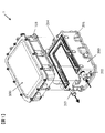
- FIG. 1 is an external perspective view showing an embodiment of a power conversion device including a DC-DC converter device and an inverter device of the present invention.
- the external appearance perspective view which looked at the DC-DC converter apparatus illustrated in FIG. 1 from the bottom face side.
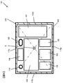
- FIG. 2 is a schematic plan view of the DC-DC converter device illustrated in FIG. 1.
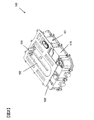
- FIG. 5 is a perspective view illustrating a mounting state of the DC-DC converter device illustrated in FIG. 4.
- the disassembled perspective view which shows one Embodiment of the high voltage side switching circuit part.
- the disassembled perspective view which shows one Embodiment of a low-voltage circuit board part.
- FIG. 6 is a plan view showing a modification of the first embodiment.
- FIG. 3 is a schematic plan view of a DC-DC converter device according to a second embodiment.
- FIG. 1 is an external perspective view of a power conversion device including the DC-DC converter device of the present invention
- FIG. 2 is an external perspective view of the DC-DC converter device shown in FIG.
- the power converter 1 is obtained by integrating a DC-DC converter device 100 and an inverter device 200.
- FIG. 1 shows the DC-DC converter device 100 and the inverter device 200 separated from each other.
- the DC-DC converter device 100 is fixed to the upper surface side of the case of the inverter device 200 with a plurality of bolts.
- the power conversion device 1 is applied to a vehicle such as an electric vehicle or a plug-in hybrid vehicle, and the inverter device 200 drives a traveling motor with electric power from an on-vehicle high voltage storage battery.
- the vehicle is equipped with a low voltage storage battery for operating auxiliary equipment such as a light and a radio, and the DC-DC converter device 100 converts power from a high voltage storage battery to a low voltage storage battery or a high voltage from a low voltage storage battery. Perform power conversion to storage battery.
- a cooling flow path 204 through which a cooling medium flows is formed in the case 201 of the inverter device 200 in order to cool the heat generating components in the inverter device 200.
- the cooling medium flows into the cooling channel from the inlet pipe 202 and flows out from the outlet pipe 203.
- the cooling channel is formed in a U shape so as to connect the inlet pipe 202 and the outlet pipe 203 along the outer peripheral side wall of the case 201 of the inverter device 200.
- the bottom surface portion 102 of the case member 101 of the DC-DC converter device 100 is fixed so as to face the inverter device 200.
- the DC-DC converter device 100 functions as a lid that covers the upper opening of the cooling flow path 204 when the inverter device 200 is fixed.
- the wall surface is the bottom surface portion 102 of the DC-DC converter device 100 and the upper surface side of the cooling flow path 204.
- the DC-DC converter device 100 is directly cooled by a cooling medium such as cooling water flowing through the cooling flow path 204.
- a seal such as an O-ring is provided between the bottom surface portion 102 of the case member 101 of the DC-DC converter device 100 and the top surface portion of the inverter device 200 so that the cooling medium in the cooling flow path 204 does not leak. ) Is provided.
- a mixture of antifreeze and water in a ratio of 1: 1 is generally suitable as the cooling medium.
- other cooling media can be used.
- a flow path wall 151 is provided on the bottom surface portion 102 of the DC-DC converter device 100 so as to project into the cooling passage 204 of the inverter device 200 and divide the flow of the cooling medium.
- an opening 152 that forms a U-shaped cooling passage through which the cooling medium divided by the flow path wall 151 flows is formed in the bottom surface portion 102 of the DC-DC converter device 100.
- the cooling medium flowing into the cooling flow path 204 from the inlet pipe 202 of the inverter device 200 is divided by the flow path wall 151 of the DC-DC converter apparatus 100 and also flows into the opening 152 of the DC-DC converter apparatus 100. .
- the cooling medium that has flowed into the opening 152 of the DC-DC converter device 100 flows in a U-shape and returns to the cooling flow path 204 again.
- the bottom surface portion 102 of the DC-DC converter device 100 serves as a lid member for the cooling flow path 204, and the DC-DC converter device 100 is effectively prevented by the cooling medium flowing in the opening 152. Can be cooled.
- the power conversion device constituted by the inverter device 200 and the DC-DC converter device 100 shows one embodiment, and the shape and structure of each device can be applied with various modifications. It is.
- the cooling device that cools the inverter device 200 and the DC-DC converter device 100 is shown as an embodiment.
- a cooling device that uses a cooling gas such as air may be used. There is no.
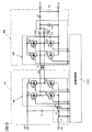
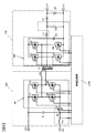
- FIG. 3 is a diagram showing an embodiment of a circuit configuration of the DC-DC converter device 100.
- a DC-DC converter device 100 shown as an embodiment of the present invention is a bidirectional DC-DC converter.
- the DC-DC converter device 100 includes a high voltage side switching circuit unit 107, a low voltage side switching circuit unit 150, and a transformer (Tr) provided between the high voltage side switching circuit unit 107 and the low voltage side switching circuit unit 150. 103). Switching control of the high voltage side switching circuit unit 107 and the low voltage side switching circuit unit 150 is performed by the control circuit unit CTR.
- the high voltage side switching circuit unit 107 is connected to MOSFETs (switching elements) H1 to H4, a choke coil Lr, a smoothing capacitor Cn, an IGBT switch H0, and an IGBT switch H0 connected as an H bridge type switching circuit.
- a shunt resistor Ri and a choke coil Lc are provided.
- the smoothing capacitor element Cn is disposed on the input side of the H-bridge type switching circuit, and smoothes the input current input to the high voltage side switching circuit unit 107.
- a gate resistor (not shown) is connected to the gate terminals of the switching elements H1 to H4.
- the control circuit unit CTR can measure a potential difference between both ends of the shunt resistor Ri and detect a high-voltage current.
- the choke coil Lc is disposed between the high voltage power supply HV ( ⁇ ) and the shunt resistor Ri and functions as a normal mode filter.
- the high voltage circuit board 40 surrounded by a broken line in FIG. 3, wirings for connecting the switching elements H1 to H4 constituting the high voltage side switching circuit unit 107 in an H bridge are provided.
- the high voltage circuit board 40 also includes power semiconductor modules 35 to be described later which are switching elements H1 to H4, a power semiconductor module 36 which is an IGBT switch H0, a smoothing capacitor 38 (Cn), and other electronic components other than the resonance coil Lr. Are mounted, and their wiring patterns are also provided.
- the high voltage side switching circuit unit 107 will be described later with reference to FIG.
- the low voltage side switching circuit unit 150 includes MOSFETs (switching elements) S3 and S4 that constitute a synchronous rectifier circuit and MOSFETs (switching elements) S1 that constitute an active clamp circuit in order to ensure high output on the low voltage side.
- MOSFETs switching elements
- S3 and S4 that constitute a synchronous rectifier circuit
- MOSFETs switching elements
- S1 that constitute an active clamp circuit in order to ensure high output on the low voltage side.
- S2 reactors L1 and L2 configured as a full-wave rectification type double current (current doubler), an output capacitor Co, a noise filter inductor Lf, and a capacitor Cf.
- the gate resistances of the MOSFETs S1 to S4 are not shown.
- the low voltage circuit board portion 108 In the low voltage circuit board portion 108 surrounded by a broken line in FIG. 3, wirings for connecting the switching elements S1 to S4 constituting the low voltage side switching circuit portion 150 are provided. On the low-voltage circuit board portion 108, electronic components other than the reactors L1 and L2 among the electronic components shown in FIG. 3 are mounted and their wiring patterns are also provided.
- the low voltage circuit board unit 108 will be described later with reference to FIG.
- the switching circuit and smooth reactor small reactors (L1, L2) are arranged in two circuits in parallel so as to have symmetry, thereby increasing the output.
- L1, L2 The switching circuit and smooth reactor small reactors
- an active clamp circuit using MOSFETs S1 and S2 having freewheeling diodes is provided to reduce the breakdown voltage of the switching element by suppressing the generation of surge voltage during switching, thereby reducing the breakdown voltage of the circuit components.
- the device is downsized.
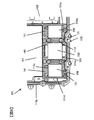
- FIG. 4 is a schematic plan view of the DC-DC converter device shown in FIG. 1
- FIG. 5 is a perspective view showing a mounted state of the DC-DC converter device shown in FIG.
- the case member 101 of the DC-DC converter device 100 is made of a conductive metal such as an aluminum metal.
- the bottom surface portion 102 of the case member 101 has a substantially rectangular shape in a plan view, and an outer peripheral side wall 115 raised substantially perpendicular to the bottom surface portion 102 is integrally formed on the outer periphery of the bottom surface portion 102.
- a plurality of storage chambers are provided by partition walls 111a to 111f described later.
- These storage chambers are provided with a transformer 103, choke coils 104 and 105, a noise filter coil 106, a power semiconductor module 35 that constitutes switching elements H1 to H4, a smoothing capacitor 38, and the like. 107, a low-voltage circuit board portion 108 provided with switching elements S1 to S4 and the like are accommodated. The arrangement of these electronic components will be described later.
- the transformer 103 corresponds to the transformer Tr
- the choke coils 104 and 105 correspond to the reactors L1 and L2 of the current doubler
- the noise filter coil 106 corresponds to the noise filter inductor Lf. Yes.
- the outer peripheral side wall 115 of the case member 101 includes a first long side 115a on the lower side in FIGS. 4 and 5, a second long side 115b on the upper side in FIGS. 4 and 5, and a first long side on the left side in FIGS. It is composed of a short side 115c and a second long side 115d on the right side of FIGS.
- the first partition wall 111a installed in parallel with the lower first long side 115a and the upper second long side 115b are installed in parallel.
- the second partition wall 111b, the third partition wall 111c installed in parallel with the second short side 115d on the right side, and the first long side 115a on the lower side and orthogonal to the long side 115a
- the fourth to sixth three partition walls 111d, 111e, and 111f installed at predetermined intervals are installed.
- the first storage chamber in which the low-voltage circuit board unit 108 is stored is partitioned by the first partition wall 111a, the second partition wall 111b, the third partition wall 111c, and the first short side 115c on the left side.
- the second storage chamber in which the high-voltage side switching circuit unit 107 is stored is partitioned by the third partition wall 111c, the second short side 115d on the right side, and the first and second long sides 115a and 115b.
- the third storage chamber in which the choke coil 104 is stored is partitioned by the first partition wall 111a, the fourth partition wall 111d, the fifth partition wall 111e, and the first long side 115a.
- partition walls constitute a storage chamber together with the outer peripheral wall 115 of the case member 101 as a partition wall member.
- the fourth storage chamber in which the transformer 103 is stored is partitioned by the first partition wall 111a, the fifth partition wall 111e, the sixth partition wall 111f, and the first long side 115a.
- These partition walls constitute a storage chamber together with the outer peripheral wall 115 of the case member 101 as a partition wall member.
- the fifth storage chamber in which the choke coil 105 is stored is partitioned by the first partition wall 111a, the sixth partition wall 111f, the third partition wall 111c, and the first long side 115a.
- These partition walls constitute a storage chamber together with the outer peripheral wall 115 of the case member 101 as a partition wall member.
- the sixth storage chamber in which the noise filter coil 106 is stored is partitioned by the second partition wall 111b, the upper second long side 115b, and the left first short side 115c.
- the third to fifth containment rooms are arranged side by side from left to right along the long side 115a. That is, the transformer 103 is disposed in the fourth storage chamber so that one side surface thereof directly faces one long side 115 a of the outer peripheral side wall 115.
- the choke coils 104 and 105 are respectively arranged so that one side faces the long side 115a of the outer peripheral side wall 115 directly. That is, the transformer 103 and the choke coils 104 and 105 are constrained by the surrounding wall members.
- the first storage chamber is disposed above the third to fifth storage chambers, that is, inside the case member 101 from the transformer 103 and the choke coils 104 and 105.
- the low voltage circuit board portion 108 accommodated in the first accommodating chamber has one side surface on the short side directly facing the short side 115c on the left side of the outer peripheral side wall 115, and the longitudinal direction thereof is the first and first side.
- the two partition walls 111a and 111b are arranged in parallel. That is, the low voltage circuit board portion 108 is restrained by the surrounding wall member.
- the low voltage circuit board part 108 is arranged so that a part thereof is located on the center C of the rectangular region of the bottom part 102 of the case member 101. That is, in FIG. 4, the straight line indicated by two two-dot chain lines is a diagonal line of the bottom surface part 102 having a rectangular shape, and the low voltage circuit board part 108 is placed on the center C indicated by a double circle at the intersection of the diagonal lines. Is installed.
- the low voltage circuit board unit 108 is mounted with the active clamp circuit and the switching elements S1 to S4 of the synchronous rectifier circuit, the output capacitor Co, and the like surrounded by a dotted line in FIG. Is provided.
- the sixth storage chamber is disposed between the low voltage circuit board portion 108 and the other long side 115c of the outer peripheral side wall 115, that is, between the second partition wall 111b and the long side 115b.
- the noise filter coil 106 accommodated in the sixth accommodating chamber is disposed so that one side surface thereof directly faces the other long side 115 b of the outer peripheral side wall 115.
- the second storage chamber is provided between the third partition wall 111c and the right short side 115d.
- the high-voltage side switching circuit unit 107 housed in the second housing chamber is arranged such that one side surface of the long side faces the short side 115d on the right side of the outer peripheral side wall 115 directly.
- the other side surface on the long side of the high voltage side switching circuit unit 107 is arranged to face the other side surface on the short side of the low voltage circuit board unit 108 and one side surface of the choke coil 105, that is, the third partition wall 111c. ing.
- the voltage-side switching circuit unit 107 is constrained by the surrounding wall members and is arranged in a direction substantially perpendicular to the longitudinal direction of the low-voltage circuit board unit 108.
- the high voltage side switching circuit unit 107 includes a high voltage circuit board 40 on which wirings for connecting the switching elements H1 to H4 and the switching elements H1 to H4 to the bridge circuit are formed, as will be described later.
- the high voltage circuit board 40 is mounted with a choke coil Lc and a shunt resistor Ri. That is, on the high voltage circuit board 40, electronic components other than the switching elements H1 to H4 are mounted among the electronic components in the region surrounded by the dotted line in FIG.
- an opening 109 for high-voltage power supply and an opening 110 for low-voltage power output are provided on both sides of the noise filter coil 106, respectively. Is formed.
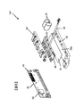
- FIG. 6 is an exploded perspective view showing an embodiment of the high voltage side switching circuit unit 107.
- the high voltage side switching circuit unit 107 configured as a high voltage module includes a high voltage circuit board 40, power semiconductor modules 35 and 36, a metal base 30, a leaf spring 33, a temperature sensor 34, and a smoothing capacitor element 38.
- the power semiconductor module 35 corresponds to the MOSFETs H1 to H4 in FIG. 3
- the power semiconductor module 36 corresponds to the IGBT switch H0 in FIG.
- the smoothing capacitor element 38 corresponds to the smoothing capacitor Cn of FIG.
- the choke coil Lr can be integrated into the high voltage module shown in FIG. 6 or can be installed separately.
- the metal base 30 is formed by, for example, aluminum die casting or the like, and is fixed to the inner surface of the bottom surface portion 102 of the case member 101 by a fastening member such as a screw.
- the metal base 30 has a recess 30a formed in the upper part, and power semiconductor modules 35 and 36 are disposed in the recess 30a.
- the power semiconductor modules 35 and 36 are pressed against each other by a leaf spring 33 disposed above the power semiconductor modules 35 and 36, and are in contact with the bottom surface of the concave portion of the metal base 30 through an insulating sheet 31 having good thermal conductivity.
- the leaf spring 33 is fixed to the inner surface of the bottom surface portion 102 of the case member 101 by a fastening member such as a screw.
- the metal base 30 for example, a material having high thermal conductivity such as A6063 can be used, and the case member 101 can be made of a general aluminum die casting material such as ADC12 type. Thereby, compared with the case where the metal base 30 is not attached and the entire case member 101 is formed of a material having high thermal conductivity, the material cost can be reduced.
- Thermally conductive grease (not shown) between the inner surface of the bottom surface portion 102 of the case member 101 and the metal base 30, between the metal base 30 and the insulating sheet 31, and between the insulating sheet 31 and the power semiconductor modules 35 and 36. Is applied.
- the bottom surface portion 102 of the case member 101 constitutes the cooling flow path 204 together with the inverter device 200, and the heat generated from the heat generating members such as the power semiconductor modules 35 and 36 circulates in the cooling flow path 204. Cooled by the cooling medium.
- the smoothing capacitor 38 is accommodated in a capacitor case (not shown) fixed to the metal base 30.
- This capacitor case is disposed above the leaf spring 33 that press-contacts the power semiconductor modules 35 and 35 with a slight gap from the leaf spring 33.
- the temperature sensor 34 is fixed to the metal base 30 by a fastening member such as a screw.
- the temperature sensor 34 is connected to the control circuit unit CTR illustrated in FIG. 3 by a harness.
- the temperature sensor 34 detects the temperature of the power semiconductor modules 35 and 36 via the metal base 30 and transmits the detection signal to the control circuit unit CTR.
- the control circuit unit CTR determines whether or not an abnormality has occurred based on the temperature information transmitted from the temperature sensor 34. If it is determined that there is an abnormality, the output from the DC-DC converter device 100 is limited. Perform protection control.
- the high voltage circuit board 40 is mounted so as to rise substantially perpendicularly to the bottom surface portion 102 of the case member 101.
- the lower end surface of the high-voltage circuit board 40 is located in the vicinity of the inner surface of the bottom surface portion 102 of the case member 101 and covers the sides of the power semiconductor modules 35 and 36 attached to the metal base 30. By doing so, the width (height) of the high voltage circuit board 40 is widened, the area of the high voltage circuit board 40 is increased, and the internal space of the case member 101 is effectively utilized.
- Lead terminals of the power semiconductor modules 35 and 36 are connected to the high voltage circuit board 40.
- the lead terminals of the power semiconductor modules 35 and 36 are inserted into terminal holes provided in the high voltage circuit board 40 and soldered.
- the switching elements H 1 to H 4 of the four power semiconductor modules 35 connected to the high voltage circuit board 40 are connected as an H bridge circuit by wiring provided on the high voltage circuit board 40.
- a connector 41 having a plurality of connector pins on the upper side is mounted on the high voltage circuit board 40.
- a control circuit board on which the control circuit unit CTR shown in FIG. 3 is formed is arranged on the upper side of the case member 101. Each connector pin of the connector 41 is provided on the control circuit board. The pin hole is inserted and soldered.
- the control circuit unit CTR and the power semiconductor modules 35 and 36 are electrically connected by a connector 41, and the control circuit unit CTR performs switching control of the power semiconductor module 35 and on / off control of the power semiconductor module 36.
- a choke coil 42 (Lc in FIG. 3) is mounted on the high voltage circuit board 40.
- the choke coil 42 is electrically connected between the (+) or ( ⁇ ) of the high voltage power supply and the H bridge circuit, and functions as a normal mode filter.
- the two smoothing capacitor elements 38 are connected in parallel by a connecting bus bar and connected to the high voltage circuit board 40.
- the high voltage circuit board 40 is exemplified as a structure in which the high voltage circuit board 40 is raised and fixed substantially perpendicularly to the inner surface of the bottom surface portion 102 of the case member 101.
- the high voltage circuit board 40 may be arranged on the upper side of the power semiconductor modules 35 and 36 and / or the smoothing capacitor element 38 in parallel with the inner surface of the bottom surface portion 102 of the case member 101.
- the power semiconductor modules 35 and 36 may be directly brought into contact with the inner surface of the bottom surface portion 102 of the case member 101 without using the metal base 30.
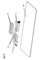
- FIG. 7 is an exploded perspective view of the low-voltage circuit board unit 108.
- the low-voltage circuit board portion 108 includes a base substrate 50 formed of an aluminum-based metal having good thermal conductivity. Although not shown, an insulating film is formed on one surface of the base substrate 50, and wirings constituting the active clamp circuit and the synchronous rectifier circuit shown in FIG. 3 are formed on the insulating film. As described above, the low-voltage circuit board portion 108 includes the power semiconductor module 51 (corresponding to the switching elements S1 to S4), the output capacitor 52 (Co in FIG. 3), and the active clamp circuit capacitor 53 (Cc in FIG. 3). It is mounted with solder.
- the power semiconductor module 51 is a surface mount MOSFET package, the bottom surface of which is made of metal such as copper, and has the same potential as the drain electrode of the MOSFET chip inside the module.
- a good heat dissipation structure that also serves as an electrical connection can be formed by connecting the wiring with the solder.
- the transformer 103 and the choke coils 104 and 105 are connected to the low voltage circuit board unit 108 by bus bars 121, 122 and 123, respectively.
- the noise filter coil 106 is connected to the low voltage circuit board 108 by a bus bar 124.
- the high-voltage side switching circuit unit 107 is connected to the transformer 103 by a bus bar.
- the transformer 103, the choke coils 104 and 105, the noise filter coil 106, the high voltage side switching circuit unit 107, and the low voltage circuit board unit 108 are arranged in the case member 101 of the DC-DC converter device 100.
- the low voltage circuit board portion 108 is disposed on the center C of the rectangular region of the bottom surface portion 102 of the case member 101.
- the transformer 103 and the choke coils 104 and 105 are located along the one long side 115a of the outer peripheral side wall 115 of the case member 101 at a position deviated from the center C of the rectangular region of the bottom surface portion 102 of the case member 101. Directly facing each other.
- the high voltage side switching circuit portion 107 is directly opposed along the other short side 115d of the outer peripheral side wall 115 of the case member 101 at a position deviated from the center C of the rectangular region of the bottom surface portion 102 of the case member 101. Are arranged.
- the low voltage circuit board unit 108 has a weight of about 200 to 300 g, for example.
- the weight of the transformer 103 is about 250 to 350 g, for example, and the weights of the choke coils 104 and 105 are about 150 to 250 g, respectively.
- the rectangular area of the low voltage circuit board 108 is about 4 to 5 times that of the transformer 103 and about 6 to 8 times that of the choke coils 104 and 105. Therefore, the weight per unit area of the transformer 103 is the largest, and the choke coils 104 and 105 are also larger than the low voltage circuit board portion 108, respectively.
- the weight is 250 g to 350 g, and the area is only slightly smaller than that of the low voltage side switching circuit unit 108 as shown in FIG. However, the weight per unit area is larger than that of the low-voltage circuit board unit 108.
- the height of the transformer 103 and the choke coils 104 and 105 is, for example, about 25 to 40 mm, and is larger than the thickness of the low-voltage circuit board portion 108 (height from the inner surface of the bottom surface portion 102 of the case member 101).
- the high voltage side switching circuit unit 107 is thicker than the low voltage circuit board unit 108 because the smoothing capacitor 38 is disposed above the power semiconductor modules 35 and 36.
- a part having a large weight and height per unit area is disposed facing the outer peripheral side wall 115 of the case member 101, and the weight and thickness (height per unit area) are determined.
- the low-voltage circuit board portion 108 with a small) is arranged so that a part thereof is located on the center C of the rectangular region of the bottom surface portion 102 of the case member 101. For this reason, it is excellent with respect to vibration resistance or impact resistance.
- FIG. 8 is a plan view showing a modification of the first embodiment.
- the transformer 103 and the choke coils 104 and 105 are disposed in the accommodating portion 131 formed by one long side 115a of the outer peripheral side wall 115 and the partition walls 111d, 111e, and 111f, respectively.
- the modification is characterized in that a resin 141 is filled in each accommodating portion 131 formed by one long side 115a of the outer peripheral side wall 115 and the partition walls 111d to 111f.
- Each of the transformer 103 and the choke coils 104 and 105 disposed in each housing portion 131 is fixed with its outer peripheral side surface covered with a resin 141. For this reason, the transformer 103 and the choke coils 104 and 105 can be fixed more reliably, and vibration resistance or impact resistance can be improved.
- the height of the partition walls 111a to 111f may be lower than the outer peripheral side wall 115, and may be about 1/3 or more of the height of each component.
- the electronic components 103, 104, and 105 that are heavy and high in height are arranged facing the long side 115 a of the outer peripheral side wall 115. Further, in the modification, it has been described that these electronic components 103 to 105 are fixed by sealing the periphery with resin. In the first embodiment and the modification, the electronic components 103 to 105 are fastened to the bottom surface portion 102 of the base member 101 by fastening with fastening members.
- FIG. 9 is a diagram showing a circuit configuration as a second embodiment of the DC-DC converter device of the present invention. 9 is different from FIG. 3 in that a center tap is provided on the secondary coil side of the transformer Tr, the reactor L1 is connected between the center tap and the positive electrode of the low-voltage power supply output unit, and the reactor L2 is removed. It is. Other than that, the configuration is the same as that illustrated in FIG. 3, and the corresponding components are denoted by the same reference numerals and description thereof is omitted.
- FIG. 10 is a schematic plan view showing one embodiment of a mounted state of the circuit shown in FIG.
- the noise filter coil 106 is disposed at the place where the choke coil 105 is disposed on the bottom surface portion 102 of the case member 101 in the first embodiment.
- the high voltage side switching circuit unit 107 is moved to one long side 115a side of the outer peripheral side wall 115, and the positions of the opening 109 for high voltage power supply input and the opening 110 for low voltage power output are the high voltage side switching circuit unit. 107 and the other long side 115c of the outer peripheral side wall 115 are moved. Then, the low-voltage circuit board portion 108 is moved closer to the position where the noise filter coil 106 was disposed, and is disposed close to the other long side 115 c of the outer peripheral side wall 115.
- the low-voltage circuit board portion 108 has one side surface on the short side side along one short side 115b of the outer peripheral side wall 115 and one side surface on the long side side along the other long side 115c of the outer peripheral side wall 115. Directly facing each other.
- a mounting structure in which no components are mounted on the center C of the rectangular region of the bottom surface portion 102 of the case member 101 is obtained. That is, the low-voltage circuit board portion 108 can also be mounted at a position off the center C of the rectangular area of the bottom surface portion 102 of the case member 101.
- the center of the rectangular area of the bottom surface portion 102 of the case member 101 has the smallest strength.
- the vibration resistance or the shock resistance of the DC-DC converter device 100 can be obtained by adopting a structure in which no parts are arranged near the center C. Can be further improved.
- An electronic component having a large weight and height per unit area such as the transformer 103 and the choke coils 104 and 105, is arranged along one long side 115a of the outer peripheral side wall 115 of the case member 101 of the DC-DC converter device 100.
- the structure is arranged directly facing each other. Therefore, these parts can be supported and restrained by the outer peripheral side wall 115.
- the low voltage circuit board portion 108 having a small weight and thickness (height) per unit area is disposed on the center C of the rectangular region of the bottom surface portion 102 of the case member 101 (Embodiment 1), or A structure (Embodiment 2) in which none of the components are arranged is employed. For this reason, in combination with the above (1), the DC-DC converter device 100 can have excellent vibration resistance or shock resistance.
- the partition walls 111a to 111f are integrally formed on the bottom surface portion 102 of the case member 101, and together with the outer peripheral side wall 115, the transformer 103, choke coils 104 and 105, the low voltage circuit board portion 108, and the high voltage side switching circuit.
- Each of the portions 107 is formed with a storage portion 131 that stores the portion 107. For this reason, the transformer 103, the choke coils 104 and 105, the low-voltage circuit board unit 108, and the high-voltage side switching circuit unit 107 are supported and restrained, and the vibration resistance or shock resistance of the DC-DC converter device 100 is increased. Can be improved.
- Resin 141 is filled in each accommodating portion 131 that accommodates the transformer 103 and the choke coils 104 and 105 to cover the outer peripheral side surfaces of the transformer 103 and the choke coils 104 and 105 to increase the fixing strength. For this reason, the vibration resistance or the shock resistance of the DC-DC converter device 100 can be improved.
- the bus bars 121 to 124 are used to connect the transformer 103, the choke coils 104 and 105, the noise filter coil 106, and the low voltage circuit board unit 108, and the transformer 103 and the high voltage side switching circuit unit 107. Yes.
- the low-voltage circuit board portion 108 and the high-voltage circuit board 40 can be formed separately from one control circuit board, and the area of the control circuit board is reduced, so that the DC-DC converter The vibration resistance or impact resistance of the apparatus 100 can be improved.
- the high voltage side switching circuit unit 107 employs a structure in which the power semiconductor modules 35 and 36 are pressed against the metal base 30. For this reason, by using a material having high thermal conductivity for the metal base 30, the case member 101 can be made of a normal inexpensive metal material, and the cost can be reduced.
- the power conversion device 1 is configured by fixing the bottom surface portion 102 of the DC-DC converter device 100 to the inverter device 200 in which the cooling flow path 204 through which the cooling medium flows is formed. Therefore, the DC-DC converter device 100 and the inverter device 200 can be efficiently cooled.
- a flow path wall 151 that divides the cooling flow path 204 of the inverter device 200 is provided on the bottom surface portion 102 of the DC-DC converter apparatus 100, and communicates from one surface of the flow path wall 151 to the other surface.
- a U-shaped opening 152 was provided. The cooling medium flows into the opening 152 through the flow path wall 151, flows through the opening 152, and returns to the cooling flow path 204. Since the DC-DC converter device 100 is directly cooled by the cooling medium while the cooling medium flows through the opening 152, the cooling efficiency of the DC-DC converter device 100 is excellent.
- the transformer 103, the choke coils 104 and 105, the noise filter coil 106, the low-voltage circuit board portion 108, and the high-voltage side mounted on the inner surface of the bottom surface portion 102 of the case member 101 shown in the first and second embodiments.
- the arrangement of the switching circuit unit 107 is merely an example, and various modifications can be made.
- the transformer 103 may be disposed at the corner of the case member 101.
- the arrangement of the high voltage side switching circuit unit 107 may be replaced with the arrangement of the transformer 103 and the choke coils 104 and 105, and the high voltage side switching circuit unit 107 may be arranged almost in parallel with the low voltage circuit board unit 108.
- a noise filter capacitor Cf may be mounted on the bottom surface portion 102 of the case member 101. Further, a resonance capacitor element and a resonance coil constituting a resonance circuit may be connected in series to the primary side of the main transformer Tr, and zero voltage switching (ZVS) may be performed at a high switching frequency (100 kHz). Switching loss can be reduced and conversion efficiency can be improved. Further, a noise filter capacitor may be added to the input section of the high voltage side switching circuit section. A resonance capacitor and / or a noise filter capacitor may be mounted on the bottom surface portion 102 of the case member 101.
- the smoothing capacitor element 38 (Cn), the resonance capacitor Cc, and the noise filter capacitor Cy may be accommodated in one case to constitute a capacitor module.
- the capacitor module is a constituent member of the high voltage side switching circuit unit 107.
- the capacitor module is preferably disposed at a position directly facing along at least one side of the outer peripheral side wall 115 of the case member 101.
- the DC-DC converter device 100 that is integrated with the inverter device 200 and constitutes the power conversion device 1 is exemplified.
- the DC-DC converter device 100 of the present invention can be integrated into a device other than the inverter device 200, or can be mounted alone at a predetermined mounting position.
- the power converter device 1 mounted in vehicles such as an electric vehicle and a plug-in hybrid vehicle, was demonstrated to the example, this invention is not limited to these, The power converter device used for vehicles, such as a construction machine, It can also be applied to.
- the present invention can be applied with various modifications within the scope of the gist of the present invention.
- the outer peripheral side wall is provided on the bottom surface of the case member of the DC-DC converter device, Is at least one side faced directly along one side of the outer peripheral side wall of the case member, and is the low voltage side switching circuit portion placed on the center of the rectangular area of the bottom face portion of the case member?
- any structure may be used as long as no parts are arranged.
Landscapes
- Engineering & Computer Science (AREA)
- Power Engineering (AREA)
- Transportation (AREA)
- Mechanical Engineering (AREA)
- Life Sciences & Earth Sciences (AREA)
- Sustainable Development (AREA)
- Sustainable Energy (AREA)
- Dc-Dc Converters (AREA)
Abstract
高出力化を図り、体積や重量の大きい部品を搭載しても、耐振動性あるいは耐衝撃性に優れたDC-DCコンバータ装置を提供する。 トランス103、チョークコイル104、105は、ケース部材101の外周側壁115の一長辺115aに沿って配置され、高電圧側スイッチング回路部107は、外周側壁115の一短辺115dに沿って配置されている。そして、単位面積当たりの重量が小さい低電圧回路基板部108は、その一部が底面部102の矩形領域の中心上に位置するように配置されている。
Description
本発明は、高出力であっても、小型化が可能であり、かつ、耐振動性あるいは耐衝撃性に優れたDC-DCコンバータ装置および電力変換装置に関する。
電気自動車やプラグインハイブリッド車は、動力駆動用の高電圧蓄電池でモータ駆動するためのインバータ装置および車両のライトやラジオなどの補機を作動させるための低電圧蓄電池を備えている。このような車両には、高電圧蓄電池から低電圧蓄電池への電力変換または低電圧蓄電池から高電圧蓄電池への電力変換を行うDC-DCコンバータ装置が搭載されている。
DC-DCコンバータ装置は、高電圧の直流電流を交流電流に変換する高電圧側スイッチング回路、交流高電圧を交流低電圧に変換するトランス、低電圧交流電圧を直流電流に変換する低電圧スイッチング回路を備えている。
従来のDC-DCコンバータ装置として、トランス、高電圧側スイッチング回路および低電圧側スイッチング回路を構成する電子部品を配線基板上に実装し、この配線基板を、放熱フィンを有する冷却ブロックに固定した構造が知られている(例えば、特許文献1参照)。
上記特許文献1では、1枚の配線基板上に、DC-DCコンバータ装置を構成するすべての電子部品を配置する構造である。このため、大出力とするために、トランス等の部品として体積や重量の大きいものを用いると、耐振動性あるいは耐衝撃性が低下する。
本発明のDC-DCコンバータ装置は、トランスと、トランスの一次側に接続された高電圧側スイッチング回路部と、トランスの二次側に接続された低電圧回路基板部、および少なくとも一つのチョークコイルを含む低電圧側スイッチング回路部と、トランス、高電圧側スイッチング回路部、および低電圧側スイッチング回路を収容するケース部材と、を備える。ケース部材は、底面部と、底面部の外周に沿って立ち上げて形成された外周側壁とを有し、少なくともトランスは、少なくとも一側面がケース部材の外周側壁の一側辺に沿って、直接、対面して配置され、ケース部材の底面部の矩形領域の中心上には、低電圧回路基板部が配置されているか、または部品が配置されていないことを特徴とする。
本発明によれば、ケース部材の中心上には低電圧回路基板部がされるか、または、部品が配置されておらず、ケース部材の外周側壁に沿って配置されたトランスは、外周側壁によって支持されるので、耐振動性あるいは耐衝撃性を向上することができる。
-実施形態1-
[電力変換装置]
以下、図面を参照して、本発明のDC-DCコンバータ装置および電力変換装置の一実施の形態について説明する。
図1は、本発明のDC-DCコンバータ装置を備える電力変換装置の外観斜視図であり、図2は、図1に図示されたDCーDCコンバータ装置を底面側からみた外観斜視図である。
電力変換装置1は、DC-DCコンバータ装置100とインバータ装置200とを一体化したものであり、図1ではDC-DCコンバータ装置100とインバータ装置200とを分離した状態で示されている。DC-DCコンバータ装置100は、複数のボルトによりインバータ装置200のケース上面側に固定されている。
[電力変換装置]
以下、図面を参照して、本発明のDC-DCコンバータ装置および電力変換装置の一実施の形態について説明する。
図1は、本発明のDC-DCコンバータ装置を備える電力変換装置の外観斜視図であり、図2は、図1に図示されたDCーDCコンバータ装置を底面側からみた外観斜視図である。
電力変換装置1は、DC-DCコンバータ装置100とインバータ装置200とを一体化したものであり、図1ではDC-DCコンバータ装置100とインバータ装置200とを分離した状態で示されている。DC-DCコンバータ装置100は、複数のボルトによりインバータ装置200のケース上面側に固定されている。
電力変換装置1は、電気自動車やプラグインハイブリッド車等の車両に適用され、インバータ装置200は車載の高電圧蓄電池からの電力により走行用モータを駆動する。車両にはライトやラジオなどの補機を作動させるための低電圧蓄電池が搭載されており、DC-DCコンバータ装置100は、高電圧蓄電池から低電圧蓄電池への電力変換または低電圧蓄電池から高電圧蓄電池への電力変換を行う。
インバータ装置200のケース201にはインバータ装置200内の発熱部品の冷却のため、冷却媒体が流れる冷却流路204が形成されている。冷却媒体は入口配管202から冷却流路内に流入し、出口配管203から流出する。冷却流路は、インバータ装置200のケース201の外周側壁に沿って、入口配管202と出口配管203とを連結するようにコ字形状に形成されている。一方、DC-DCコンバータ装置100のケース部材101は、その底面部102がインバータ装置200と対向して固定される。DC-DCコンバータ装置100は、インバータ装置200が固定された状態では、冷却流路204の上部開口を覆う蓋として機能する。すなわち、DC-DCコンバータ装置100の底面部102、冷却流路204の上面側の壁面となっている。これにより、DC-DCコンバータ装置100は、冷却流路204内を流通する冷却水等の冷却媒体により直接冷却される。DC-DCコンバータ装置100のケース部材101の底面部102と、インバータ装置200の上面部の間には、冷却流路204の冷却媒体が漏れ出ないように、Oリングなどのシール(図示せず)が設けられている。
本実施の形態では、冷却媒体としては不凍液と水を1:1で混合したものが一般的に適している。しかし、それ以外の冷却媒体を用いることもできる。
DC-DCコンバータ装置100の底面部102には、図2に図示されるように、インバータ装置200の冷却通路204に突出して冷却媒体の流れを分流する流路壁151が設けられている。また、DC-DCコンバータ装置100の底面部102には、流路壁151で分流された冷却媒体が流通するU字形状の冷却通路を形成する開口部152が形成されている。
DC-DCコンバータ装置100の底面部102には、図2に図示されるように、インバータ装置200の冷却通路204に突出して冷却媒体の流れを分流する流路壁151が設けられている。また、DC-DCコンバータ装置100の底面部102には、流路壁151で分流された冷却媒体が流通するU字形状の冷却通路を形成する開口部152が形成されている。
インバータ装置200の入口配管202から冷却流路204内に流入した冷却媒体は、DC-DCコンバータ装置100の流路壁151で分流され、DC-DCコンバータ装置100の開口部152内にも流入する。DC-DCコンバータ装置100の開口部152内に流入した冷却媒体は、U字形状に流通して再び冷却流路204内に還流する。開口部152内では、DC-DCコンバータ装置100の底面部102が冷却流路204の蓋部材となっており、開口部152内を流通する冷却媒体により、DC-DCコンバータ装置100を効果的に冷却することができる。
なお、上記インバータ装置200とDC-DCコンバータ装置100とにより構成される電力変換装置は、一実施の形態を示すものであり、各装置の形状・構造等は、種々、変形して適用が可能である。また、インバータ装置200とDC-DCコンバータ装置100とを冷却する冷却装置は、一実施の形態として示したものであり、他に、空気等の冷却気体を用いた冷却装置等を用いても差し支えはない。
[DC-DCコンバータ装置の回路構成]
次に、DC-DCコンバータ装置100について説明する。図3はDC-DCコンバータ装置100の回路構成の一実施の形態を示す図である。
図3に示すように、本発明の一実施の形態として示すDC-DCコンバータ装置100は、双方向DCーDCコンバータである。このDC-DCコンバータ装置100は、高電圧側スイッチング回路部107と、低圧側スイッチング回路部150と、高電圧側スイッチング回路部107と低圧側スイッチング回路部150との間に設けられたトランス(Tr)103とを備えている。高電圧側スイッチング回路部107と低圧側スイッチング回路部150のスイッチング制御は制御回路部CTRにより行われる。
次に、DC-DCコンバータ装置100について説明する。図3はDC-DCコンバータ装置100の回路構成の一実施の形態を示す図である。
図3に示すように、本発明の一実施の形態として示すDC-DCコンバータ装置100は、双方向DCーDCコンバータである。このDC-DCコンバータ装置100は、高電圧側スイッチング回路部107と、低圧側スイッチング回路部150と、高電圧側スイッチング回路部107と低圧側スイッチング回路部150との間に設けられたトランス(Tr)103とを備えている。高電圧側スイッチング回路部107と低圧側スイッチング回路部150のスイッチング制御は制御回路部CTRにより行われる。
高電圧側スイッチング回路部107は、Hブリッジ型スイッチング回路として接続されたMOSFET(スイッチング素子)H1~H4と、チョークコイルLrと、平滑コンデンサCnと、IGBTスイッチH0と、IGBTスイッチH0に接続されるシャント抵抗RiおよびチョークコイルLcとを備える。平滑コンデンサ素子Cnは、Hブリッジ型スイッチング回路の入力側に配置され、高電圧側スイッチング回路部107に入力される入力電流を平滑にする。スイッチング素子H1~H4のゲート端子には図示しないゲート抵抗が接続されている。
制御回路部CTRにより、シャント抵抗Riの両端の電位差を測定し、高電圧系の電流を検出することができる。チョークコイルLcは、高電圧電源HV(-)とシャント抵抗Riとの間に配置されており、ノーマルモードフィルタとして機能する。
図3で破線で囲った高電圧回路基板40には、高電圧側スイッチング回路部107を構成するスイッチング素子H1~H4をHブリッジ接続する配線が設けられる。高電圧回路基板40にはまた、スイッチング素子H1~H4である後述するパワー半導体モジュール35、IGBTスイッチH0であるパワー半導体モジュール36、平滑コンデンサ38(Cn)、および共振コイルLrを除くその他の電子部品が実装されるとともに、それらの配線パターンも設けられる。高電圧側スイッチング回路部107は図6で後述する。
低電圧側スイッチング回路部150は、低電圧側での高出力を確保するために、同期整流回路を構成するMOSFET(スイッチング素子)S3,S4と、アクティブクランプ回路を構成するMOSFET(スイッチング素子)S1,S2と、全波整流型の倍電流(カレントダブラー)として構成されたリアクトルL1,L2と、出力コンデンサCoと、ノイズフィルタ用のインダクタLfおよびコンデンサCfとを備えている。MOSFETS1~S4のゲート抵抗は図示を省略した。
図3で破線で囲った低電圧回路基板部108には、低電圧側スイッチング回路部150を構成するスイッチング素子S1~S4を接続する配線が設けられる。低電圧回路基板部108にはまた、図3に示す電子部品のうちリアクトルL1,L2を除く電子部品が実装されるとともに、それらの配線パターンも設けられる。低電圧回路基板部108は図7で後述する。
スイッチング回路および平滑リアクトルの小型リアクトル(L1,L2)を、対称性を持たせるように2回路並列配置とすることで高出力化している。このように、小型リアクトルを2回路配置とすることで、大型リアクトル1台を配置させる場合に比べて、DC-DCコンバータ装置全体の小型化が可能となる。加えて、還流ダイオードを持つMOSFET S1,S2を用いたアクティブクランプ回路を設けて、スイッチング時のサージ電圧発生を抑制してスイッチング素子の耐圧を低減させることで、回路部品の低耐圧化を図り、装置を小型化している。
[DC-DCコンバータ装置の構造]
図4は、図1に図示されたDC-DCコンバータ装置の模式的平面図であり、図5は、図4に図示されたDC-DCコンバータ装置の実装状態を示す斜視図である。
DC-DCコンバータ装置100のケース部材101は、アルミニウム系金属などの導電性金属により形成されている。ケース部材101の底面部102は、平面視でほぼ矩形形状を有し、底面部102の外周には、底面部102に対してほぼ垂直に立ち上げられた外周側壁115が一体に成型されている。
ケース部材101内には、後述する仕切壁111a~111fにより複数の収容室が設けられている。これらの収容室には、トランス103、チョークコイル104、105、ノイズフィルタ用コイル106、スイッチング素子H1~H4を構成するパワー半導体モジュー35や平滑コンデンサ38などが設けられている高電圧側スイッチング回路部107、スイッチング素子S1~S4などが設けられている低電圧回路基板部108等が収容されている。これらの電子部品の配置については後述する。
図3の回路図との対応を記載すると、トランス103はトランスTrに、チョークコイル104、105はカレントダブラのリアクトルL1、L2に、ノイズフィルタ用コイル106は、ノイズフィルタ用インダクタLfに対応している。
―ケース部材内での電子部品の配置―
図4及び図5を参照してケース部材内での電子部品の配置を説明する。なお、以下の説明では、上下左右とは図4及び図5の紙面内における位置関係を示す意味で使用する。
ケース部材101の外周側壁115は、図4及び5の下側の第1の長辺115aと、図4及び5の上側の第2の長辺115bと、図4及び5の左側の第1の短辺115cと、図4及び5の右側の第2の長辺115dとで構成されている。
図4及び図5を参照してケース部材内での電子部品の配置を説明する。なお、以下の説明では、上下左右とは図4及び図5の紙面内における位置関係を示す意味で使用する。
ケース部材101の外周側壁115は、図4及び5の下側の第1の長辺115aと、図4及び5の上側の第2の長辺115bと、図4及び5の左側の第1の短辺115cと、図4及び5の右側の第2の長辺115dとで構成されている。
外周側壁115で囲まれたケース部材101内には、下側の第1の長辺115aに平行に設置された第1の仕切壁111aと、上側の第2の長辺115bに平行に設置された第2の仕切壁111bと、右側の第2の短辺115dに平行に設置された第3の仕切壁111cと、下側の第1の長辺115aと直交して、かつ長辺115aに沿って所定間隔で設置された第4~第6の3枚の仕切壁111d,111e,111fとが設置されている。
低電圧回路基板部108が収容される第1の収容室は、第1の仕切壁111a、第2の仕切壁111b、第3の仕切壁111c、および、左側の第1の短辺115cにより区画されている。
高電圧側スイッチング回路部107が収容される第2の収容室は、第3の仕切壁111c、右側の第2の短辺115d、第1および第2の長辺115a,115bにより区画されている。
チョークコイル104が収容される第3の収容室は、第1の仕切壁111a、第4の仕切壁111d、第5の仕切壁111e、および第1の長辺115aにより区画されている。
これらの仕切壁は仕切壁部材としてケース部材101の外周壁部115とともに収容室を構成する。
トランス103が収容される第4の収容室は、第1の仕切壁111a、第5の仕切壁111e、第6の仕切壁111f、および第1の長辺115aにより区画されている。
これらの仕切壁は仕切壁部材としてケース部材101の外周壁部115とともに収容室を構成する。
チョークコイル105が収容される第5の収容室は、第1の仕切壁111a、第6の仕切壁111f、第3の仕切壁111c、および第1の長辺115aにより区画されている。
これらの仕切壁は仕切壁部材としてケース部材101の外周壁部115とともに収容室を構成する。
ノイズフィルタ用コイル106が収容される第6の収容室は、第2の仕切壁111b、上側の第2の長辺115b、および、左側の第1の短辺115cにより区画されている。
第3~5の収容室は長辺115aに沿って、左から右に並設されている。すなわち、第4の収容室には、トランス103が、その一側面を、直接、外周側壁115の一方の長辺115aに対面して配置されている。トランス103の両隣の第3及び第5の収容室には、チョークコイル104、105が、それぞれ、その一側面を、直接、外周側壁115の長辺115aに対面して配置されている。すなわち、トランス103、チョークコイル104、105はその周囲の壁部材で拘束されている。
第1の収容室は、第3~第5の収容室の上側に、すなわち、トランス103、チョークコイル104、105よりもケース部材101の内方に配置されている。第1の収容室に収容された低電圧回路基板部108は、その短辺側の一側面が、直接、外周側壁115の左側の短辺115cに対面し、その長手方向が、第1および第2の仕切壁111a,111bと平行にして配置されている。すなわち、低電圧回路基板部108はその周囲の壁部材で拘束されている。
低電圧回路基板部108は、その一部が、ケース部材101の底面部102の矩形領域の中心C上に位置するように配置されている。すなわち、図4において、2本の二点鎖線で示す直線は、矩形形状の底面部102の対角線であり、この対角線の交点に二重丸で示す中心C上には、低電圧回路基板部108が搭載されている。
低電圧回路基板部108は、上述したように、図3に点線で囲まれたアクティブクランプ回路及び同期整流回路のスイッチング素子S1~S4および出力コンデンサCoなどが実装されるとともに、必要な配線パターンが設けられている。
第6の収容室は、低電圧回路基板部108と、外周側壁115の他方の長辺115cとの間、すなわち、第2の仕切壁111bと長辺115bとの間に配置されている。第6の収容室に収容されたノイズフィルタ用コイル106は、その一側面が、直接、外周側壁115の他方の長辺115bに対面して配置されている。
第2の収容室は、第3の仕切壁111cと右側の短辺115dと間に設けられている。第2の収容室に収容された高電圧側スイッチング回路部107は、その長辺側の一側面が、直接、外周側壁115の右側の短辺115dに対面して配置されている。高電圧側スイッチング回路部107の長辺側の他側面は、低電圧回路基板部108の短辺側の他側面およびチョークコイル105の一側面、すなわち第3の仕切壁111cに対面して配置されている。換言すれば、電圧側スイッチング回路部107は、周囲の壁部材で拘束され、かつ、低電圧回路基板部108の長手方向とほぼ直角方向に向けて配置されている。
高電圧側スイッチング回路部107は、後述する如く、スイッチング素子H1~H4およびスイッチング素子H1~H4をブリッジ回路に接続する配線が形成された高電圧回路基板40を含んでいる。また、高電圧回路基板40には、チョークコイルLcおよびシャント抵抗Riが実装されている。つまり、高電圧回路基板40には、図3に点線で囲まれた領域内の電子部品の中、スイッチング素子H1~H4を除く電子部品が実装されている。
なお、外周側壁115の長辺115bと低電圧回路基板部108との間には、ノイズフィルタ用コイル106の両側に、高圧電源入力用の開口部109および低圧電源出力用の開口部110がそれぞれ形成されている。
―高電圧側スイッチング回路部107―
図6は、高電圧側スイッチング回路部107の一実施の形態を示す分解斜視図である。
高電圧モジュールとして構成される高電圧側スイッチング回路部107は、高電圧回路基板40、パワー半導体モジュール35、36、金属ベース30、板ばね33、温度センサ34および平滑コンデンサ素子38から構成されている。パワー半導体モジュール35は、図3のMOSFET H1~H4に対応し、パワー半導体モジュール36は、図3のIGBTスイッチH0に対応する。また、平滑コンデンサ素子38は、図3の平滑コンデンサCnに対応する。
なお、チョークコイルLrは、図6の高電圧モジュールに一体化することも、別に設置することもできる。
図6は、高電圧側スイッチング回路部107の一実施の形態を示す分解斜視図である。
高電圧モジュールとして構成される高電圧側スイッチング回路部107は、高電圧回路基板40、パワー半導体モジュール35、36、金属ベース30、板ばね33、温度センサ34および平滑コンデンサ素子38から構成されている。パワー半導体モジュール35は、図3のMOSFET H1~H4に対応し、パワー半導体モジュール36は、図3のIGBTスイッチH0に対応する。また、平滑コンデンサ素子38は、図3の平滑コンデンサCnに対応する。
なお、チョークコイルLrは、図6の高電圧モジュールに一体化することも、別に設置することもできる。
金属ベース30は、例えば、アルミダイカスト等により形成され、ケース部材101の底面部102の内面にねじ等の締結部材により固定される。金属ベース30には、上部に凹部30aが形成されており、凹部30a内にパワー半導体モジュール35、36が配置されている。パワー半導体モジュール35、36は、その上方に配置された板ばね33により圧接されて、熱伝導性の良い絶縁シート31を介して金属ベース30の凹部底面に接触している。板ばね33は、ねじ等の締結部材によりケース部材101の底面部102の内面に固定されている。
金属ベース30として、例えば、A6063のような熱伝導率が高い材料を用いることにより、ケース部材101を、例えば、ADC12タイプのような一般的なアルミダイカスト用材料を用いることが可能となる。これにより、金属ベース30を装着せず、ケース部材101全体を熱伝導率が高い材料で形成する場合に比し、材料費を安価にすることができる。
ケース部材101の底面部102の内面と金属ベース30との間、金属ベース30と絶縁シート31の間、絶縁シート31とパワー半導体モジュール35、36の間には熱伝導性グリース(図示せず)が塗布されている。上述した如く、ケース部材101の底面部102は、インバータ装置200と共に冷却流路204を構成しており、パワー半導体モジュール35、36等の発熱部材から発生した熱は、冷却流路204を循環する冷却媒体によって冷却される。
平滑コンデンサ38は、金属ベース30に固定された図示しないコンデンサケースに収容されている。このコンデンサケースは、パワー半導体モジュール35、35を圧接する板ばね33の上方に、板ばね33と僅かな空隙を存して配置される。
温度センサ34は金属ベース30にねじ等の締結部材より固定されている。温度センサ34は、ハーネスにより、図3に図示された制御回路部CTRに接続されている。温度センサ34は、金属ベース30を介してパワー半導体モジュール35、36の温度を検出し、その検出信号を制御回路部CTRに送信する。制御回路部CTRは、温度センサ34から送信される温度情報に基づいて異常発生の有無を判断し、異常有りと判断された場合には、DC-DCコンバータ装置100からの出力を制限する等の保護制御を行う。
高電圧回路基板40は、ケース部材101の底面部102に対してほぼ垂直に立ち上げて取り付けられている。高電圧回路基板40の下端面は、ケース部材101の底面部102の内面近傍に位置しており、金属ベース30に取り付けられたパワー半導体モジュール35、36の側方を覆っている。このようにすることにより、高電圧回路基板40の幅(高さ)を広くして、高電圧回路基板40の面積を大きくし、ケース部材101の内部スペースを有効に活用している。
高電圧回路基板40には、パワー半導体モジュール35、36のリード端子が接続されている。パワー半導体モジュール35、36のリード端子は、高電圧回路基板40に設けられた端子孔に挿通され、半田付けされる。
高電圧回路基板40に接続された4個のパワー半導体モジュール35のスイッチング素子H1~H4は、高電圧回路基板40に設けられた配線により、Hブリッジ回路として接続される。
高電圧回路基板40には、上部側に複数のコネクタピンを有するコネクタ41が実装されている。図示はしないが、ケース部材101の上部側には、図3に図示された制御回路部CTRが形成された制御回路基板が配置されており、コネクタ41の各コネクタピンは、制御回路基板に設けられたピン孔に挿通され、半田付けされる。制御回路部CTRとパワー半導体モジュール35、36はコネクタ41により電気的に接続され、制御回路部CTRによりパワー半導体モジュール35のスイッチング制御およびパワー半導体モジュール36のオン・オフ制御が行われる。
高電圧回路基板40には、チョークコイル42(図3のLc)が実装されている。チョークコイル42は、高電圧電源の(+)または(-)とHブリッジ回路の間に電気的に接続され、ノーマルモードフィルタとして機能する。
2個の平滑コンデンサ素子38は、図示はしないが、接続用バスバーにより並列に接続されて、高電圧回路基板40に接続されている。
なお、上記実施形態においては、高電圧回路基板40をケース部材101の底面部102の内面にほぼ垂直に立ち上げて固定した構造として例示した。しかし、高電圧回路基板40を、パワー半導体モジュール35、36および/または平滑コンデンサ素子38の上部側に、ケース部材101の底面部102の内面と平行に配置してもよい。
また、金属ベース30を用いずに、パワー半導体モジュール35、36を、直接、ケース部材101の底面部102の内面に接触させるようにしてもよい。
なお、上記実施形態においては、高電圧回路基板40をケース部材101の底面部102の内面にほぼ垂直に立ち上げて固定した構造として例示した。しかし、高電圧回路基板40を、パワー半導体モジュール35、36および/または平滑コンデンサ素子38の上部側に、ケース部材101の底面部102の内面と平行に配置してもよい。
また、金属ベース30を用いずに、パワー半導体モジュール35、36を、直接、ケース部材101の底面部102の内面に接触させるようにしてもよい。
―低電圧回路基板部108―
図7は、低電圧回路基板部108の分解斜視図である。
低電圧回路基板部108は、熱伝導性のよいアルミニウム系金属などで形成されたベース基板50を含んでいる。図示はしないが、ベース基板50の一面に絶縁膜が形成され、絶縁膜上に図3に図示されたアクティブクランプ回路や同期整流回路を構成する配線が形成されている。上述した如く、低電圧回路基板部108には、パワー半導体モジュール51(スイッチング素子S1~S4に対応)、出力コンデンサ52(図3のCo)およびアクティブクランプ回路用コンデンサ53(図3のCc)が半田により実装されている。パワー半導体モジュール51は、面実装MOSFETパッケージであって、その底面は銅等の金属で形成され、モジュール内部のMOSFETチップのドレイン電極と同電位となっており、この底面とベース基板50に形成された配線とを半田で接続することで、電気的接続も兼ねた良好な放熱構造を形成できる。
図5を参照すると、トランス103、チョークコイル104、105は、それぞれ、バスバー121、122、123により低電圧回路基板部108に接続されている。ノイズフィルタ用コイル106は、バスバー124により低電圧回路基板部108に接続されている。また、図示はしないが、高電圧側スイッチング回路部107は、バスバーによりトランス103に接続されている。
上述した如く、DC-DCコンバータ装置100のケース部材101内には、トランス103、チョークコイル104、105、ノイズフィルタ用コイル106、高電圧側スイッチング回路部107および低電圧回路基板部108が、配置されて収容されている。
つまり、図4に示すように、ケース部材101の底面部102の矩形領域の中心C上には低電圧回路基板部108が配置されている。トランス103、チョークコイル104、105は、ケース部材101の底面部102の矩形領域の中心Cから外れた位置で、上述したように、ケース部材101の外周側壁115の一方の長辺115aに沿って、直接、対面して配置されている。また、高電圧側スイッチング回路部107は、ケース部材101の底面部102の矩形領域の中心Cから外れた位置で、ケース部材101の外周側壁115の他方の短辺115dに沿って、直接、対面して配置されている。
つまり、図4に示すように、ケース部材101の底面部102の矩形領域の中心C上には低電圧回路基板部108が配置されている。トランス103、チョークコイル104、105は、ケース部材101の底面部102の矩形領域の中心Cから外れた位置で、上述したように、ケース部材101の外周側壁115の一方の長辺115aに沿って、直接、対面して配置されている。また、高電圧側スイッチング回路部107は、ケース部材101の底面部102の矩形領域の中心Cから外れた位置で、ケース部材101の外周側壁115の他方の短辺115dに沿って、直接、対面して配置されている。
低電圧回路基板部108は、例えば、重量が200~300g程度である。一方、トランス103の重量は、例えば、250~350g程度であり、チョークコイル104、105の重量は、それぞれ、150~250g程度である。図4に図示されているように、低電圧回路基板部108の矩形領域は、トランス103の4~5倍、チョークコイル104、105の6~8倍程度である。従って、単位面積当たりの重量は、トランス103が最も大きく、チョークコイル104、105も、それぞれ、低電圧回路基板部108よりも大きい。高電圧側スイッチング回路部107は、平滑コンデンサ38を備えるので、例えば、250g~350gの重量となり、図6に図示されているように、面積は低電圧側スイッチング回路部108より若干小さいだけであるが、単位面積当たりの重量が、低電圧回路基板部108よりも大きい。
トランス103およびチョークコイル104、105の高さは、例えば、25~40mm程度であり、低電圧回路基板部108の厚さ(ケース部材101の底面部102の内面からの高さ)よりも大きい。高電圧側スイッチング回路部107は、パワー半導体モジュール35、36の上部に平滑コンデンサ38が配置されるため、低電圧回路基板部108よりも厚さが大きい。
このように、本発明の一実施の形態では、単位面積当たりの重量および高さが大きい部品をケース部材101の外周側壁115に面して配置し、単位面積当たりの重量および厚さ(高さ)が小さい低電圧回路基板部108を、その一部がケース部材101の底面部102の矩形領域の中心C上に位置するように配置した。
このため、耐振動性あるいは耐衝撃性に対して優れている。
このため、耐振動性あるいは耐衝撃性に対して優れている。
(変形例)
図8は、実施形態1の変形例を示す平面図である。
上述した如く、トランス103、チョークコイル104、105は、それぞれ、外周側壁115の一方の長辺115aと仕切壁111d,111e,111fにより形成された収容部131内に配置されている。図8に図示されるように、変形例は、外周側壁115の一方の長辺115aと仕切壁111d~111fにより形成される各収容部131内に樹脂141を充填した点に特徴を有する。
図8は、実施形態1の変形例を示す平面図である。
上述した如く、トランス103、チョークコイル104、105は、それぞれ、外周側壁115の一方の長辺115aと仕切壁111d,111e,111fにより形成された収容部131内に配置されている。図8に図示されるように、変形例は、外周側壁115の一方の長辺115aと仕切壁111d~111fにより形成される各収容部131内に樹脂141を充填した点に特徴を有する。
各収容部131内に配置されたトランス103、チョークコイル104、105は、それぞれ、その外周側面が樹脂141により覆われて固定されている。このため、トランス103、チョークコイル104、105の固定がより確実となり、耐振動性あるいは耐衝撃性を向上することができる。
仕切壁111a~111fの高さは、外周側壁115よりも低くてもよく、各部品の高さの1/3程度以上であればよい。
仕切壁111a~111fの高さは、外周側壁115よりも低くてもよく、各部品の高さの1/3程度以上であればよい。
なお、以上説明した第1の実施形態では、重量が重く、かつ背丈の高い電子部品103,104,105が外周側壁115の長辺115aなどに対面して配置されていると説明した。また、変形例では、これら電子部品103~105は周囲を樹脂封止して固着すると説明した。第1の実施形態や変形例において、電子部品103~105は締結部材で締結してベース部材101の底面部102に固定されている。
―実施形態2―
図9は、本発明のDC-DCコンバータ装置の実施形態2としての回路構成を示す図である。
図9において、図3と異なる点は、トランスTrの二次コイル側にセンタータップを設け、センタータップと低電圧電源出力部の正極との間にリアクトルL1を接続し、リアクトルL2を取り除いた点である。それ以外は、図3に図示された構成と同様であり、対応する構成に同一の符号を付して説明を省略する。
図9は、本発明のDC-DCコンバータ装置の実施形態2としての回路構成を示す図である。
図9において、図3と異なる点は、トランスTrの二次コイル側にセンタータップを設け、センタータップと低電圧電源出力部の正極との間にリアクトルL1を接続し、リアクトルL2を取り除いた点である。それ以外は、図3に図示された構成と同様であり、対応する構成に同一の符号を付して説明を省略する。
図10は、図9に示された回路の実装状態の一実施の形態を示す模式的平面図である。
実施形態2に示すDC-DCコンバータ装置100では、チョークコイル104のみが必要とされ、チョークコイル105を実装する必要はない。
そこで、図10に図示されたDC-DCコンバータ装置100では、実施形態1においてケース部材101の底面部102におけるチョークコイル105が配置されていた場所に、ノイズフィルタ用コイル106が配置されている。
実施形態2に示すDC-DCコンバータ装置100では、チョークコイル104のみが必要とされ、チョークコイル105を実装する必要はない。
そこで、図10に図示されたDC-DCコンバータ装置100では、実施形態1においてケース部材101の底面部102におけるチョークコイル105が配置されていた場所に、ノイズフィルタ用コイル106が配置されている。
高電圧側スイッチング回路部107が、外周側壁115の一方の長辺115a側に移動され、高圧電源入力用の開口部109および低圧電源出力用の開口部110の位置が、高電圧側スイッチング回路部107と外周側壁115の他方の長辺115cとの間に移動されている。
そして、低電圧回路基板部108を、ノイズフィルタ用コイル106が配置されていた位置側に寄せ、外周側壁115の他方の長辺115cに近接配置させている。つまり、低電圧回路基板部108は、短辺側の一側面が外周側壁115の一方の短辺115bに、また、長辺側の一側面が外周側壁115の他方の長辺115cに沿って、直接、対面して配置されている。
そして、低電圧回路基板部108を、ノイズフィルタ用コイル106が配置されていた位置側に寄せ、外周側壁115の他方の長辺115cに近接配置させている。つまり、低電圧回路基板部108は、短辺側の一側面が外周側壁115の一方の短辺115bに、また、長辺側の一側面が外周側壁115の他方の長辺115cに沿って、直接、対面して配置されている。
このように配置することにより、図10に図示されるように、ケース部材101の底面部102の矩形領域の中心C上には、如何なる部品も搭載されない実装構造とされる。つまり、低電圧回路基板部108も、ケース部材101の底面部102の矩形領域の中心Cから外れた位置に搭載することができる。
ケース部材101の底面部102の矩形領域の中心が最も強度が小さいが、この中心C近傍には如何なる部品も配置されない構造とすることにより、DC-DCコンバータ装置100の耐振動性あるいは耐衝撃性を、一層、向上することができる。
ケース部材101の底面部102の矩形領域の中心が最も強度が小さいが、この中心C近傍には如何なる部品も配置されない構造とすることにより、DC-DCコンバータ装置100の耐振動性あるいは耐衝撃性を、一層、向上することができる。
本発明の各実施形態によれば、下記の効果を奏する。
(1)トランス103、チョークコイル104、105等の単位面積当たりの重量及び高さが大きい電子部品を、DC-DCコンバータ装置100のケース部材101の外周側壁115の一方の長辺115aに沿って、直接、対面して配置した構造としている。従って、これらの部品を外周側壁115で支持、拘束することができる。
(1)トランス103、チョークコイル104、105等の単位面積当たりの重量及び高さが大きい電子部品を、DC-DCコンバータ装置100のケース部材101の外周側壁115の一方の長辺115aに沿って、直接、対面して配置した構造としている。従って、これらの部品を外周側壁115で支持、拘束することができる。
(2)ケース部材101の底面部102の矩形領域の中心C上に、単位面積当たりの重量および厚さ(高さ)の小さい低電圧回路基板部108を配置する(実施形態1)か、あるいはいずれの部品も配置しない構造(実施形態2)としている。このため、上記(1)と相俟って、DC-DCコンバータ装置100の耐振動性あるいは耐衝撃性を優れたものとすることができる。
(3)ケース部材101の底面部102に、仕切壁111a~111fを一体に成型して、外周側壁115と共に、トランス103、チョークコイル104、105、低電圧回路基板部108、高電圧側スイッチング回路部107を、それぞれ、収容する収容部131を形成している。このため、トランス103、チョークコイル104、105、低電圧回路基板部108、高電圧側スイッチング回路部107を支持し、拘束する強度が大きくなり、DC-DCコンバータ装置100の耐振動性あるいは耐衝撃性を向上することができる。
(4)トランス103、チョークコイル104、105を収容する各収容部131内に樹脂141を充填して、トランス103、チョークコイル104、105の外周側面を覆い、固定強度を増大させている。このため、DC-DCコンバータ装置100の耐振動性あるいは耐衝撃性を向上することができる。
(4)トランス103、チョークコイル104、105を収容する各収容部131内に樹脂141を充填して、トランス103、チョークコイル104、105の外周側面を覆い、固定強度を増大させている。このため、DC-DCコンバータ装置100の耐振動性あるいは耐衝撃性を向上することができる。
(5)トランス103、チョークコイル104、105およびノイズフィルタ用コイル106と低電圧回路基板部108との接続、およびトランス103と高電圧側スイッチング回路部107との接続をバスバー121~124により行っている。このため、1枚の制御用回路基板から、低電圧回路基板部108および高電圧回路基板40を分離して形成することが可能となり、制御用回路基板の面積が小さくなるので、DC-DCコンバータ装置100の耐振動性あるいは耐衝撃性を向上することができる。
(6)高電圧側スイッチング回路部107として、金属ベース30にパワー半導体モジュール35、36を圧接して構成する構造を採用した。このため、金属ベース30として熱伝導性の高い材料を用いることにより、ケース部材101は、通常の安価な金属材料とすることが可能となり、コストを低減することができる。
(7)DC-DCコンバータ装置100の底面部102を、冷却媒体が流通する冷却流路204が形成されたインバータ装置200に固定して電力変換装置1を構成した。従って、DC-DCコンバータ装置100およびインバータ装置200を効率的に冷却することができる。
(8)DC-DCコンバータ装置100の底面部102に、インバータ装置200の冷却流路204を分流する流路壁151を設け、また、流路壁151の一方の面から他方の面に連通するU字形状の開口152を設けた。冷却媒体は、流路壁151により開口部152内に流入し、開口部152内を流通して冷却流路204内に還流する。開口部152内を冷却媒体が流通する間、DC-DCコンバータ装置100は、冷却媒体により、直接、冷却されるため、DC-DCコンバータ装置100の冷却の効率が優れたものとなる。
(8)DC-DCコンバータ装置100の底面部102に、インバータ装置200の冷却流路204を分流する流路壁151を設け、また、流路壁151の一方の面から他方の面に連通するU字形状の開口152を設けた。冷却媒体は、流路壁151により開口部152内に流入し、開口部152内を流通して冷却流路204内に還流する。開口部152内を冷却媒体が流通する間、DC-DCコンバータ装置100は、冷却媒体により、直接、冷却されるため、DC-DCコンバータ装置100の冷却の効率が優れたものとなる。
なお、上記実施形態1、2に示した、ケース部材101の底面部102の内面に実装されたトランス103、チョークコイル104、105、ノイズフィルタ用コイル106、低電圧回路基板部108および高電圧側スイッチング回路部107の配置は、一例を示すに過ぎないものであり、種々、変形が可能である。
例えば、トランス103をケース部材101の角部に配置してもよい。高電圧側スイッチング回路部107の配置をトランス103、チョークコイル104、105の配置と入れ替え、高電圧側スイッチング回路部107を低電圧回路基板部108とほぼ平行に配置してもよい。
例えば、トランス103をケース部材101の角部に配置してもよい。高電圧側スイッチング回路部107の配置をトランス103、チョークコイル104、105の配置と入れ替え、高電圧側スイッチング回路部107を低電圧回路基板部108とほぼ平行に配置してもよい。
ケース部材101の底面部102に、ノイズフィルタ用コンデンサCfを搭載するようにしてもよい。
また、主トランスTrの一次側に、共振回路を構成する共振コンデンサ素子および共振コイルを直列に接続し、高スイッチング周波数(100kHz)でゼロ電圧スイッチング(ZVS)させてもよい。スイッチング損失が低減し変換効率を向上することができる。また、高電圧側スイッチング回路部の入力部にノイズフィルタ用コンデンサを付加してもよい。共振コンデンサおよび/またはノイズフィルタ用コンデンサをケース部材101の底面部102に搭載するようにしてもよい。
また、主トランスTrの一次側に、共振回路を構成する共振コンデンサ素子および共振コイルを直列に接続し、高スイッチング周波数(100kHz)でゼロ電圧スイッチング(ZVS)させてもよい。スイッチング損失が低減し変換効率を向上することができる。また、高電圧側スイッチング回路部の入力部にノイズフィルタ用コンデンサを付加してもよい。共振コンデンサおよび/またはノイズフィルタ用コンデンサをケース部材101の底面部102に搭載するようにしてもよい。
平滑コンデンサ素子38(Cn)、共振コンデンサCc、ノイズフィルタ用コンデンサCyを1つのケース内に収容してコンデンサモジュールを構成するようにしてもよい。この場合、コンデンサモジュールは、高電圧側スイッチング回路部107の構成部材となる。コンデンサモジュールは、ケース部材101の外周側壁115の少なくとも一側辺に沿って、直接、対面する位置に配置することが好ましい。
上記実施形態では、インバータ装置200に一体化されて電力変換装置1を構成するDC-DCコンバータ装置100として例示した。しかし、本発明のDC-DCコンバータ装置100は、インバータ装置200以外の装置に一体化したり、あるいは、単独で所定の取付位置に装着したりすることができるものである。また、上記実施形態では、電気自動車やプラグインハイブリッド車等の車両に搭載される電力変換装置1を例に説明したが、本発明はこれらに限らず建設機械等の車両に用いられる電力変換装置にも適用することができる。
その他、本発明は、本発明の趣旨の範囲内において、種々、変形して適用することが可能であり、要は、DC-DCコンバータ装置のケース部材の底面部に外周側壁を設け、トランスの少なくとも一側面をケース部材の外周側壁の一側辺に沿って、直接、対面して配置し、ケース部材の底面部の矩形領域の中心上には、低電圧側スイッチング回路部が配置されているか、または、部品が配置されていない構造としたものであればよい。
1 電力変換装置
35、36 パワー半導体モジュール(H1~H4、H0)
38 平滑コンデンサ素子(Cn)
40 高電圧回路基板
42 チョークコイル(Lc)
50 低電圧回路基板
51 パワー半導体モジュール(S1~S4)
100 DC-DCコンバータ装置
101 ケース部材
102 底面部
103 トランス(Tr)
104、105 チョークコイル(L1、L2)
106 ノイズフィルタ用コイル(Lf)
107 高電圧側スイッチング回路部
108 低電圧回路基板部
111a~111f 仕切壁
115 外周側壁
115a、115b 長辺
115c、115d 短辺
121~124 バスバー
131 収容部
141 樹脂
150 低電圧側スイッチング回路部
151 流路壁
152 開口部
200 インバータ装置
CTR 制御回路部
Claims (15)
- トランスと、
前記トランスの一次側に接続された高電圧側スイッチング回路部と、
前記トランスの二次側に接続された低電圧回路基板部、および少なくとも一つのチョークコイルを含む低電圧側スイッチング回路部と、
前記トランス、前記高電圧側スイッチング回路部、および前記低電圧側スイッチング回路を収容するケース部材と、を備え、
前記ケース部材は、底面部と、前記底面部の外周に沿って立ち上げて形成された外周側壁とを有し、
少なくとも前記トランスは、少なくとも一側面が前記ケース部材の外周側壁の一側辺に沿って、直接、対面して配置され、
前記ケース部材の底面部の矩形領域の中心上には、前記低電圧回路基板部が配置されているか、または部品が配置されていないことを特徴とするDC-DCコンバータ装置。 - 請求項1に記載のDC-DCコンバータ装置において、
前記トランスの高さおよび単位矩形領域当たりの重量は、それぞれ、前記低電圧回路基板部の高さおよび単位面積当たりの重量よりも大きいことを特徴とするDC-DCコンバータ装置。 - 請求項2に記載のDC-DCコンバータ装置において、
前記ケース部材は、前記外周側壁と共に前記トランスの周囲を囲む仕切壁部材を備え、前記外周側壁と前記仕切壁によって構成される収容部内に前記トランスの外周側面を覆う樹脂が充填されていることを特徴とするDC-DCコンバータ装置。 - 請求項1に記載のDC-DCコンバータ装置において、
前記少なくとも一つの第1のチョークコイルは、少なくとも一側面が前記ケース部材の外周側壁の一側辺に沿って配置され、前記第1のチョークコイルの高さおよび単位面積当たりの重量は、それぞれ、前記低電圧回路基板部の高さおよび単位面積当たりの重量よりも大きいことを特徴とするDC-DCコンバータ装置。 - 請求項4に記載のDC-DCコンバータ装置において、
前記ケース部材は、前記外周側壁と共に、前記トランスの外周を囲む第1の仕切壁部材と、前記外周側壁と共に、前記第1のチョークコイルの外周を囲む第2の仕切壁部材とを備え、前記外周側壁と前記第1の仕切壁部材によって構成される第1の収容部内に前記トランスの外周側面を覆う樹脂が充填され、前記外周側壁と前記第2の仕切壁部材によって構成される第2の収容部内に前記第1のチョークコイルの外周側面を覆う樹脂が充填されていることを特徴とするDC-DCコンバータ装置。 - 請求項4に記載のDC-DCコンバータ装置において、
前記低電圧側スイッチング回路部は、さらに前記第1のチョークコイルと並列接続される第2のチョークコイルを備え、前記第2のチョークコイルは、少なくとも一側面が前記ケース部材の外周側壁の一側辺に沿って配置され、前記第2のチョークコイルの高さおよび単位面積当たりの重量は、それぞれ、前記低電圧回路基板部の高さおよび単位面積当たりの重量よりも大きいことを特徴とするDC-DCコンバータ装置。 - 請求項6に記載のDC-DCコンバータ装置において、
前記ケース部材は、前記外周側壁と共に、前記トランスの外周を囲む第1の仕切壁部材と、前記外周側壁と共に、前記第1のチョークコイルの外周を囲む第2の仕切壁部材と、前記外周側壁と共に、前記第2のチョークコイルの外周を囲む第3の仕切壁部材とを備え、前記外周側壁と前記第1の仕切壁部材によって構成される第1の収容部内に前記トランスの外周側面を覆う樹脂が充填され、前記外周側壁と前記第2の仕切壁部材によって構成される第2の収容部内に前記第1のチョークコイルの外周側面を覆う樹脂が充填され、前記外周側壁と前記第3の仕切壁部材によって構成される第3の収容部内に前記第2のチョークコイルの外周側面を覆う樹脂が充填されていることを特徴とするDC-DCコンバータ装置。 - 請求項6に記載のDC-DCコンバータ装置において、
さらに、前記低電圧回路基板部と前記トランスを接続する第1のバスバーと、前記低電圧回路基板部と前記第1のチョークコイルを接続する第2のバスバーと、前記低電圧回路基板部と前記第2のチョークコイルを接続する第3のバスバーとを備えることを特徴とするDC-DCコンバータ装置。 - 請求項1に記載のDC-DCコンバータ装置において、
さらに、前記チョークコイルの後段に設けられてノイズ成分をキャンセルするためのノイズフィルタ用コイルを備え、前記ノイズフィルタ用コイルは、前記ケース部材の外周側壁と前記低電圧回路基板部との間に配置されていることを特徴とするDC-DCコンバータ装置。 - 請求項9に記載のDC-DCコンバータ装置において、
さらに、前記ノイズフィルタ用コイルと前記低電圧回路基板部とを接続する第4のバスバーを備えることを特徴とするDC-DCコンバータ装置。 - 請求項1に記載のDC-DCコンバータ装置において、
前記低電圧回路基板部は、少なくとも1つの短辺側が前記ケース部材の外周側壁の一側辺に沿って、直接、対面して配置されていることを特徴とするDC-DCコンバータ装置。 - 請求項11に記載のDC-DCコンバータ装置において、
前記低電圧回路基板部の前記1つの短辺は、前記トランスが対面する前記外周側壁とは異なる側壁の外周側壁に対面していることを特徴とするDC-DCコンバータ装置。 - 請求項11に記載のDC-DCコンバータ層において、
前記高電圧側スイッチング回路部は、その長手方向が前記低電圧回路基板部とは、ほぼ直交する方向に向けて配置されていることを特徴とするDC-DCコンバータ装置。 - 請求項1乃至13のいずれか1項に記載のDC-DCコンバータ装置と、
前記DC-DCコンバータ装置の前記底面部に固定されたインバータ装置とを備え、
前記DC-DCコンバータ装置の底面部と前記インバータ装置との境界部に、冷却媒体が流通する冷却流路が形成されていることを特徴とする電力変換装置。 - 請求項14に記載の電力変換装置において、
前記冷却流路は、前記インバータ装置のケースの内周面に沿って形成されると共に、前記DC-DCコンバータ装置の底面部に、前記冷却流路に突出され、第1の流路と第2の流路に分流する流路壁と、前記第1の流路および前記第2の流路を連通する開口部とが形成され、前記第1の流路を流通する冷却媒体が、前記流路壁に遮断されて前記第1の流路から前記開口部を経由して前記第2の流路に戻るように流通することを特徴とする電力変換装置。
Applications Claiming Priority (2)
| Application Number | Priority Date | Filing Date | Title |
|---|---|---|---|
| JP2012-185506 | 2012-08-24 | ||
| JP2012185506A JP5926651B2 (ja) | 2012-08-24 | 2012-08-24 | Dc−dcコンバータ装置および電力変換装置 |
Publications (1)
| Publication Number | Publication Date |
|---|---|
| WO2014030499A1 true WO2014030499A1 (ja) | 2014-02-27 |
Family
ID=50149809
Family Applications (1)
| Application Number | Title | Priority Date | Filing Date |
|---|---|---|---|
| PCT/JP2013/070412 Ceased WO2014030499A1 (ja) | 2012-08-24 | 2013-07-29 | Dc-dcコンバータ装置および電力変換装置 |
Country Status (2)
| Country | Link |
|---|---|
| JP (1) | JP5926651B2 (ja) |
| WO (1) | WO2014030499A1 (ja) |
Cited By (1)
| Publication number | Priority date | Publication date | Assignee | Title |
|---|---|---|---|---|
| WO2025126753A1 (ja) * | 2023-12-15 | 2025-06-19 | サンデン株式会社 | 電子部品の耐振構造及びそれを備えた熱媒体加熱装置 |
Families Citing this family (7)
| Publication number | Priority date | Publication date | Assignee | Title |
|---|---|---|---|---|
| JP6349265B2 (ja) * | 2015-01-28 | 2018-06-27 | オムロン株式会社 | 双方向dc−dcコンバータ、パワーコンディショナ及び分散型電源システム |
| JP2016171705A (ja) * | 2015-03-13 | 2016-09-23 | パナソニックIpマネジメント株式会社 | 電源装置 |
| CN109964548B (zh) | 2016-11-17 | 2021-08-27 | Lg伊诺特有限公司 | Dc-dc转换器 |
| WO2018093195A1 (ko) * | 2016-11-17 | 2018-05-24 | 엘지이노텍 주식회사 | 직류-직류 컨버터 |
| US10912232B2 (en) * | 2016-12-09 | 2021-02-02 | Mitsubishi Electric Corporation | Electronic circuit board and power conversion device |
| KR102725755B1 (ko) * | 2019-01-28 | 2024-11-04 | 에이치엘만도 주식회사 | 전기 자동차용 배터리 충전 장치 |
| KR20240081170A (ko) * | 2022-11-30 | 2024-06-07 | 엘지이노텍 주식회사 | 전력변환장치 |
Citations (8)
| Publication number | Priority date | Publication date | Assignee | Title |
|---|---|---|---|---|
| JP2000102252A (ja) * | 1998-09-25 | 2000-04-07 | Denso Corp | 電力変換装置 |
| JP2003244959A (ja) * | 2002-02-20 | 2003-08-29 | Tdk Corp | スイッチング電源とその製造方法 |
| JP2006261368A (ja) * | 2005-03-17 | 2006-09-28 | Toyota Motor Corp | 電子部品収容構造体 |
| JP2006288052A (ja) * | 2005-03-31 | 2006-10-19 | Tdk Corp | Dc−dcコンバータ |
| JP2006288091A (ja) * | 2005-03-31 | 2006-10-19 | Tdk Corp | フィルタ回路および電源装置 |
| JP2008312413A (ja) * | 2007-06-18 | 2008-12-25 | Shindengen Electric Mfg Co Ltd | 液冷電力変換装置 |
| JP2011024408A (ja) * | 2009-06-19 | 2011-02-03 | Tdk Corp | スイッチング電源装置 |
| JP2012156298A (ja) * | 2011-01-26 | 2012-08-16 | Sanken Electric Co Ltd | Dc/dcコンバータモジュール |
-
2012
- 2012-08-24 JP JP2012185506A patent/JP5926651B2/ja active Active
-
2013
- 2013-07-29 WO PCT/JP2013/070412 patent/WO2014030499A1/ja not_active Ceased
Patent Citations (8)
| Publication number | Priority date | Publication date | Assignee | Title |
|---|---|---|---|---|
| JP2000102252A (ja) * | 1998-09-25 | 2000-04-07 | Denso Corp | 電力変換装置 |
| JP2003244959A (ja) * | 2002-02-20 | 2003-08-29 | Tdk Corp | スイッチング電源とその製造方法 |
| JP2006261368A (ja) * | 2005-03-17 | 2006-09-28 | Toyota Motor Corp | 電子部品収容構造体 |
| JP2006288052A (ja) * | 2005-03-31 | 2006-10-19 | Tdk Corp | Dc−dcコンバータ |
| JP2006288091A (ja) * | 2005-03-31 | 2006-10-19 | Tdk Corp | フィルタ回路および電源装置 |
| JP2008312413A (ja) * | 2007-06-18 | 2008-12-25 | Shindengen Electric Mfg Co Ltd | 液冷電力変換装置 |
| JP2011024408A (ja) * | 2009-06-19 | 2011-02-03 | Tdk Corp | スイッチング電源装置 |
| JP2012156298A (ja) * | 2011-01-26 | 2012-08-16 | Sanken Electric Co Ltd | Dc/dcコンバータモジュール |
Cited By (2)
| Publication number | Priority date | Publication date | Assignee | Title |
|---|---|---|---|---|
| WO2025126753A1 (ja) * | 2023-12-15 | 2025-06-19 | サンデン株式会社 | 電子部品の耐振構造及びそれを備えた熱媒体加熱装置 |
| JP2025095955A (ja) * | 2023-12-15 | 2025-06-26 | サンデン株式会社 | 電子部品の耐振構造及びそれを備えた熱媒体加熱装置 |
Also Published As
| Publication number | Publication date |
|---|---|
| JP2014045547A (ja) | 2014-03-13 |
| JP5926651B2 (ja) | 2016-05-25 |
Similar Documents
| Publication | Publication Date | Title |
|---|---|---|
| JP5926651B2 (ja) | Dc−dcコンバータ装置および電力変換装置 | |
| JP5818754B2 (ja) | Dc−dcコンバータ装置 | |
| JP6045340B2 (ja) | Dc−dcコンバータ装置 | |
| JP6175556B2 (ja) | 電力変換装置 | |
| JP5855899B2 (ja) | Dc−dcコンバータ及び電力変換装置 | |
| US10128770B2 (en) | Converter and electric power conversion apparatus | |
| JP6104347B1 (ja) | 電力変換装置 | |
| JP5914290B2 (ja) | 電力変換装置 | |
| JP6169181B2 (ja) | Dc−dcコンバータ装置 | |
| WO2013015106A1 (ja) | 電力変換装置 | |
| JP6218150B2 (ja) | 電力変換装置 | |
| JP6945671B2 (ja) | 電力変換装置 | |
| WO2013061799A1 (ja) | 電力変換装置 | |
| JP6161550B2 (ja) | 電力変換装置 | |
| JP4396627B2 (ja) | 電力変換装置 | |
| JP6962347B2 (ja) | 電力変換装置 | |
| JP7366082B2 (ja) | 電力変換装置 | |
| JP4075734B2 (ja) | 半導体装置の実装構造 | |
| JP2014131395A (ja) | Dc−dcコンバータ装置および共振コイルユニット | |
| JP2019170158A (ja) | 電力変換装置 | |
| JP7276554B2 (ja) | 直流直流コンバータ装置 | |
| WO2017170184A1 (ja) | 電力変換装置 | |
| JP5609811B2 (ja) | 電源装置 | |
| WO2019244624A1 (ja) | 電力変換装置 | |
| WO2025182101A1 (ja) | 電力変換装置 |
Legal Events
| Date | Code | Title | Description |
|---|---|---|---|
| 121 | Ep: the epo has been informed by wipo that ep was designated in this application |
Ref document number: 13830249 Country of ref document: EP Kind code of ref document: A1 |
|
| NENP | Non-entry into the national phase |
Ref country code: DE |
|
| 122 | Ep: pct application non-entry in european phase |
Ref document number: 13830249 Country of ref document: EP Kind code of ref document: A1 |