WO2014017793A1 - 금속입자층 형성 방법 및 이를 이용하여 제조된 발광소자 - Google Patents
금속입자층 형성 방법 및 이를 이용하여 제조된 발광소자 Download PDFInfo
- Publication number
- WO2014017793A1 WO2014017793A1 PCT/KR2013/006540 KR2013006540W WO2014017793A1 WO 2014017793 A1 WO2014017793 A1 WO 2014017793A1 KR 2013006540 W KR2013006540 W KR 2013006540W WO 2014017793 A1 WO2014017793 A1 WO 2014017793A1
- Authority
- WO
- WIPO (PCT)
- Prior art keywords
- acid
- metal
- light emitting
- indium
- layer
- Prior art date
- Legal status (The legal status is an assumption and is not a legal conclusion. Google has not performed a legal analysis and makes no representation as to the accuracy of the status listed.)
- Ceased
Links
Images


Classifications
-
- H—ELECTRICITY
- H10—SEMICONDUCTOR DEVICES; ELECTRIC SOLID-STATE DEVICES NOT OTHERWISE PROVIDED FOR
- H10H—INORGANIC LIGHT-EMITTING SEMICONDUCTOR DEVICES HAVING POTENTIAL BARRIERS
- H10H20/00—Individual inorganic light-emitting semiconductor devices having potential barriers, e.g. light-emitting diodes [LED]
- H10H20/80—Constructional details
- H10H20/81—Bodies
-
- H—ELECTRICITY
- H10—SEMICONDUCTOR DEVICES; ELECTRIC SOLID-STATE DEVICES NOT OTHERWISE PROVIDED FOR
- H10H—INORGANIC LIGHT-EMITTING SEMICONDUCTOR DEVICES HAVING POTENTIAL BARRIERS
- H10H20/00—Individual inorganic light-emitting semiconductor devices having potential barriers, e.g. light-emitting diodes [LED]
- H10H20/80—Constructional details
- H10H20/882—Scattering means
Definitions
- the present invention relates to a method of forming a metal layer having an uneven structure by a simpler method and a method of manufacturing a light emitting device capable of improving light extraction efficiency using the same.
- a light emitting device is a semiconductor device that generates light by flowing a current through a PN junction in a forward direction.
- Light emitting devices using semiconductors are attracting attention in next-generation lighting equipment applications because they have high efficiency for converting electrical energy into light energy, have a long lifespan of more than 5 to 10 years, and can greatly reduce power consumption and maintenance costs. .
- a sapphire substrate is mainly used for growing a gallium nitride compound semiconductor for manufacturing a light emitting device.
- a low-power gallium nitride-based light emitting device is fabricated by placing a sapphire substrate with a crystal structure on a lead frame and then connecting two electrodes to the top.
- the sapphire substrate is thinned to a thickness of about 80 microns or less and attached to the lead frame. Since the thermal conductivity of the sapphire substrate is about 50 W / m ⁇ K, even if its thickness is about 80 microns, the thermal resistance is very large, so that it is difficult to obtain a desired heat emission specification.
- a flip chip bonding method is used to further improve heat dissipation characteristics.
- Flip chip bonding inverts a chip made of a light emitting diode structure to a submount such as a silicon wafer (thermal conductivity of about 150 W / m ⁇ K) having excellent thermal conductivity or an AlN ceramic substrate (180 W / m ⁇ K of thermal conductivity).
- a submount such as a silicon wafer (thermal conductivity of about 150 W / m ⁇ K) having excellent thermal conductivity or an AlN ceramic substrate (180 W / m ⁇ K of thermal conductivity).
- heat dissipation efficiency may be improved than when heat is released through the sapphire substrate.
- the degree of improvement is not satisfactory and the manufacturing process is complicated. .
- a vertical LED manufactured by removing a sapphire substrate has been attracting attention.
- Vertical LEDs can be manufactured by removing and packaging the sapphire substrate by a laser lift-off (LLO) method from the light emitting structure and are known to have the best heat dissipation efficiency.
- LLO laser lift-off
- the laser lift-off method has an advantage in that the manufacturing process is simple, unlike the flip chip bonding method.
- the light emitting area is about 60% of the chip area, whereas in the case of the vertical LED with the sapphire substrate removed, the light emitting area is about 90% of the chip area. Excellent properties.
- the vertical LED with the sapphire substrate removed shows a lower light extraction efficiency than the conventional light emitting device because of the following reasons.
- a light emitting device is fabricated by covering an LED structure from which a sapphire substrate is removed and a molding material such as epoxy or a molding material mixed with phosphors.
- a molding material such as epoxy or a molding material mixed with phosphors.
- GaN gallium nitride
- a large portion of is not emitted to the outside but totally reflected and then proceeds toward the light emitting structure again and disappears.
- the refractive index of gallium nitride is about 2.6, if the refractive index of the molding material is assumed to be about 1.5, the amount of light totally reflected at the bonding surface of the two materials is about 9%, which requires much improvement in light extraction efficiency.
- an object of the present invention is to provide a method for forming a metal layer having a concave-convex structure in a simpler process and a light emitting device that can improve the light extraction efficiency using the same. .
- Base material that can be oxidized to generate electrons
- the substrate is oxidized by the organic acid activator to generate electrons
- the metal particle layer may have a nano-sized uneven structure.
- the irregularities may be one having a height of 10 to 1,000nm.
- the substrate may include one or more selected from the group consisting of indium, tin, zinc, aluminum, gallium, antimony, iridium, ruthenium, nickel, silver, and gold.
- the substrate may further include removing a metal oxide film formed by meeting oxygen in air.
- the forming of the metal particle layer may be performed by immersing the substrate in the activation solution one or more times.
- the metal compound is any one selected from the group consisting of metal salts, metal oxides and metal hydrates including palladium, silver, gold, copper, gallium, titanium, tantalum, ruthenium, tin, platinum or alloys thereof. It may contain the above.
- the concentration of the metal compound in the activation solution may be 0.001 to 5g / L.
- the organic acid activator may be an organic acid having 1 to 10 carbon atoms.
- the organic acid activator citric acid (citric acid), oxalic acid (oxalic acid), malonic acid (malonic acid), malic acid (malic acid), tartaric acid, acetic acid (acetic acid), fumaric acid (fumaric acid) , Lactic acid, formic acid, propionic acid, propionic acid, butyric acid, iminodiacetic acid, glyoxylic acid and ascorbic acid It may include any one or more selected from the group.
- the organic acid activator may be aliphatic polycarboxylic acid having 2 to 10 carbon atoms.
- the complexing agent may include any one or more selected from the group consisting of HCl, HF, and NHF 3 .
- the activation solution may further include an alkylene glycol monoalkyl ether.
- the present invention also provides a device comprising a metal particle layer made of metal particles precipitated by reduction of a metal compound, prepared by the above-described method.
- a light emitting device in which a light emitting structure, an electrode layer, and a metal particle layer are sequentially formed on a substrate, wherein the metal particle layer is formed of metal particles precipitated by reduction of a metal compound according to the above-described method.
- a light emitting device is provided.
- the light emitting structure may have a structure in which the n-type semiconductor layer / active layer / p-type semiconductor layer is sequentially stacked.
- the electrode layer is indium tin oxide (ITO), indium zinc oxide (IZO), indium zinc tin oxide (IZTO), indium aluminum zinc oxide (IAZO), indium gallium zinc oxide (IGZO), Using at least one selected from the group consisting of indium gallium tin oxide (IGTO), aluminum zinc oxide (AZO), antimony tin oxide (ATO), gallium zinc oxide (GZO), IrOx, RuOx, Ni, Ag, and Au It may be formed.
- ITO indium tin oxide
- IZO indium zinc oxide
- IZTO indium aluminum zinc oxide
- IAZO indium aluminum zinc oxide
- IGZO indium gallium zinc oxide
- IrOx IrOx
- RuOx Ni, Ag, and Au It may be formed.
- the light emitting device may be a low power light emitting diode, a high power flip type light emitting diode, a vertical light emitting diode, or an organic light emitting diode.
- the metal compound layer is reduced by a wet process of contacting the metal compound with an activation solution containing an organic acid activator to precipitate metal particles, thereby forming a metal particle layer having an uneven structure.
- the metal particle layer according to the present invention is applied to a light emitting device, the light extraction efficiency of the light emitting device can be improved by a simpler process.
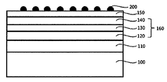
- FIG. 2 is a view showing an optical path when an uneven structure metal particle layer is formed on an electrode layer according to an embodiment of the present invention.
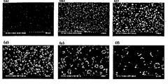
- FIG 3 is a photograph of the surface of the uneven structure metal particle layer according to the magnification using a scanning electron microscope (SEM) according to an embodiment of the present invention.
- SEM scanning electron microscope
- first and second are used to describe various components, and the terms are used only for the purpose of distinguishing one component from another component.
- each layer or element when each layer or element is referred to as being formed “on” or “on” of each layer or element, it means that each layer or element is formed directly on each layer or element, or It is meant that a layer or element can additionally be formed between each layer, on the object, the substrate.
- the method according to the present invention comprises the step of contacting a substrate capable of being oxidized to generate electrons with an activation solution comprising a metal compound, an organic acid activator, and a complexing agent, wherein the substrate is formed by the organic acid activator. It is oxidized to generate electrons, and the metal compound is reduced by the electrons to precipitate as metal particles on the surface of the substrate to form a metal particle layer.
- the metal particle layer since the metal particle layer is formed by the metal particles precipitated by the reduction reaction of the metal compound, it may include a plurality of naturally-sized nano-sized uneven structure.
- the nano-size corresponds to the size of the metal particles of the uneven structure is stone w, can be several tens of nanometers to thousands of nanosizes.
- the metal particle layer may form an uneven structure having a height of about 10 to about 1,000 nm, preferably about 30 to about 500 nm.
- the height of the uneven structure can be controlled by adjusting the contact time or the number of times of contact between the substrate and the activation solution. For example, by repeatedly immersing the substrate in the activation solution several times or more times, more metal particles can be precipitated to increase the height of the uneven structure.
- the substrate may include one or more selected from the group consisting of indium, tin, zinc, aluminum, gallium, antimony, iridium, ruthenium, nickel, silver, and gold.
- the substrate includes a component that can be oxidized by contact with an organic acid activator to generate electrons.
- the substrate may be a transparent electrode of the light emitting device, in this case indium tin oxide (ITO), indium zinc oxide (IZO), indium zinc tin oxide (IZTO), indium aluminum zinc oxide), IGZO (indium gallium zinc oxide), IGTO (indium gallium tin oxide), AZO (aluminum zinc oxide), ATO (antimony tin oxide), GZO (gallium zinc oxide), IrOx, RuOx, Ni, Ag, Au It may include any one or more selected from the group consisting of. Examples of when two or more components are included may be RuOx / ITO, Ni / IrOx / Au, and Ni / IrOx / Au / ITO.
- the concentration of the metal compound in the activation solution may be about 0.001 to about 5 g / L, preferably about 0.001 to about 0.5 g / L. If the concentration is too low, less than 0.001 g / L, the metal nanoparticles can not be formed, if the concentration is too high exceeding 5 g / L there is a problem that the metal particles are too large.
- the activator is characterized in that the organic acid, not the inorganic acid.
- the organic acid activator serves to promote a reduction reaction of the metal compound.
- the organic acid activator may be an organic acid having 1 to 10 carbon atoms, and promotes reduction of the metal compound without excessively etching the substrate as compared to the inorganic acid, and thus is more advantageous for forming the metal particle layer of the nanostructure.
- the organic acid activator citric acid (citric acid), oxalic acid (oxalic acid), malonic acid (malonic acid), malic acid (malic acid), tartaric acid, acetic acid (acetic acid), fumaric acid (fumaric acid) , Lactic acid, formic acid, propionic acid, propionic acid, butyric acid, iminodiacetic acid, glyoxylic acid and ascorbic acid It may include any one or more selected from the group.
- the formation of the metal particle layer may be easier.
- the aliphatic polycarboxylic acid having 2 to 10 carbon atoms is used, the uneven structure of the metal particle layer is further increased. It is most preferable because it can be formed finely and uniformly.
- the complexing agent serves to form ligands with the metal ions of the metal compound.
- HF HF, NHF 4 , or HCl
- HCl hydrochloric acid
- the complexing agent forms a ligand with metal ions of the metal compound and then reacts with the metal of the metal compound to precipitate nano-sized metal particles on the surface of the substrate.
- metal ions of the metal compound For example, when palladium chloride is used as the metal compound and hydrochloric acid is used as the complexing agent, palladium particles may be precipitated on the surface of the substrate by a reaction as in Scheme 1 below to form a metal particle layer having an uneven structure.
- the activation solution may further include an alkylene glycol monoalkyl ether for stability of the solution.
- the alkylene glycol monoalkyl ether is, for example, ethylene glycol monoethyl ether, ethylene glycol monobutyl ether, propylene glycol monomethyl ether, propylene glycol monoethyl ether, propylene glycol monobutyl ether, diethylene glycol monomethyl ether, di Ethylene glycol monoethyl ether, diethylene glycol monopropyl ether, diethylene glycol monobutyl ether, dipropylene glycol monomethyl ether, dipropylene glycol monoethyl ether, dipropylene glycol monopropyl ether, dipropylene glycol monobutyl ether, triethylene Glycol monomethyl ether, triethylene glycol monoethyl ether, triethylene glycol monopropyl ether, triethylene glycol monobutyl ether, tripropylene glycol monomethyl ether,
- the method for forming a metal particle layer according to the present invention can be used to manufacture a variety of devices that require nano-sized uneven structure. For example, there is a light emitting element.
- a light emitting device in which a light emitting structure, an electrode layer, and a metal particle layer are sequentially formed on a substrate, wherein the metal particle layer is formed of metal particles precipitated by reduction of a metal compound according to the above-described method.
- a light emitting device is provided.
- the light emitting device using the method for forming a metal particle layer of the present invention forming a light emitting structure on a substrate, forming an electrode layer on the light emitting structure, and forming a metal particle layer on the electrode layer by using a wet method according to the present invention. It can be prepared by the step.
- the light emitting device manufactured according to the present invention has a metal particle layer having an uneven structure on the electrode layer by depositing metal nanoparticles by a wet process of metal salt reduction in order to minimize the total internal reflection of light emitted from the light emitting structure. It is characterized by forming.
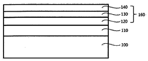
- FIGS. 1A to 1C are cross-sectional views schematically illustrating a structure according to a manufacturing process of a light emitting device according to an embodiment of the present invention.
- a light emitting structure 160 is first formed on a substrate 100 for manufacturing a light emitting device according to an embodiment of the present invention.
- the substrate 100 may be formed of, for example, at least one of sapphire (Al 2 O 3 ), silicon carbide (SiC), gallium nitride (GaN), zinc oxide (ZnO), or aluminum nitride (AlN). .
- the substrate 100 may be a sapphire substrate.
- Sapphire (Al 2 O 3 ) is a crystal in which alumina is grown as a single crystal at 2300 ° C. or more.
- the sapphire (Al 2 O 3 ) is chemically and thermally stable and thus has a high temperature process and has a high binding energy and dielectric constant.
- the light emitting structure 160 may be formed by growing a plurality of nitride-based semiconductor layers.
- the light emitting structure 160 includes, for example, an n-type semiconductor layer 120, an active layer 130, and a p-type semiconductor layer 140, and electrons and p-types provided from the n-type semiconductor layer 120. Holes provided from the semiconductor layer 140 may be recombined in the active layer 130 to generate light.
- the n-type semiconductor layer 120 and the p-type semiconductor layer 140 may be a gallium nitride-based semiconductor material having a composition formula of Al x Ga (1-x) N (where 0 ⁇ x ⁇ 1), and the gallium nitride By controlling the component ratio of the compound, a light emitting diode from a long wavelength to a short wavelength can be freely produced.
- the n-type semiconductor layer 120 is a layer for supplying electrons to the active layer 130 and may be formed of a GaN layer or a GaN / AlGaN layer doped with n-type conductive impurities.
- n-type conductive impurity for example, Si, Ge, Sn or the like can be used.
- the n-type semiconductor layer 120 is a Si-doped GaN layer Or a GaN / AlGaN layer.
- the n-type semiconductor layer 120 is illustrated as a single layer in FIGS. 1A to 1C, the n-type semiconductor layer 120 may be formed as a single layer or a multilayer, but the present invention is not limited thereto.
- the active layer 130 is formed on the n-type semiconductor layer 120 and may be formed of an InGaN / GaN layer having a multi-quantum well structure, or may be formed of one quantum well layer or a double hetero structure. have.
- the p-type semiconductor layer 140 may be formed of a GaN layer or a GaN / AlGaN layer doped with a p-type conductive impurity.
- a p-type conductive impurity for example, Mg, Zn, Be or the like can be used.
- the p-type semiconductor layer 140 may be formed of a GaN layer or a GaN / AlGaN layer doped with Mg.
- the p-type semiconductor layer 140 is illustrated as a single layer in FIGS. 1A to 1C, the p-type semiconductor layer 140 may also be formed as a single layer or a multilayer, and the present invention is not limited thereto. Accordingly, the light emitting structure 160 may include at least one of an N-P junction, a P-N junction, an N-P-N junction, and a P-N-P junction structure.
- a buffer layer 110 may be further formed between the light emitting structure 160 and the substrate 100 to alleviate the lattice constant difference between the two.
- the buffer layer 110 may be formed of a pure undoped GaN layer, and may be omitted depending on the characteristics of the device and the process conditions.
- the light emitting structure 160 may be an organic light emitting diode (OLED) having a top emission or a bottom emission structure.
- OLED organic light emitting diode
- An organic light emitting diode is an element that emits light when an exciton formed by recombining injected electrons and holes in an organic material by arranging an organic material layer between two electrodes and applying an electric field to a ground state.
- the organic light emitting diodes may be classified into various materials according to materials, light emitting mechanisms, light emitting directions, driving methods, and the like.
- the organic light emitting diodes may be divided into bottom emission and bottom glass emitting light toward the glass substrate. It can be divided into a top emission (emission).
- the manufacturing method of the light emitting device of the present invention can be applied to the organic light emitting diode of the bottom emission (for example, bottom emission) can improve the light extraction efficiency.
- an electrode layer 150 is formed on the light emitting structure 160 after the light emitting structure 160 is formed.
- the electrode layer 150 may be a transparent conductive layer having electrical conductivity.
- the electrode layer 150 may be indium tin oxide (ITO), indium zinc oxide (IZO), indium zinc tin oxide (IZTO), indium aluminum zinc oxide (IAZO), indium gallium zinc oxide (IGZO), or indium IGTO (IGTO).
- the electrode layer 150 may be formed by an e-beam evaporation method or a sputtering method, but is not limited thereto. Conventionally used methods may be used.
- the electrode layer 150 meets oxygen in the air and may naturally generate a metal oxide film. Therefore, the process of removing the metal oxide film may be further performed.
- the metal oxide film removing process may be performed by immersing the substrate on which the light emitting structure 160 and the electrode layer 150 are formed in an organic acid solution.
- the organic acid may be the same as or different from the activator added to the activation solution.
- citric acid oxalic acid, malonic acid, malic acid, malic acid, tartaric acid, acetic acid, fumaric acid, lactic acid
- Organic acids such as formic acid, propionic acid, butyric acid, iminodiacetic acid, glyoxylic acid, or ascorbic acid.
- the metal particle layer 200 including the nano-sized uneven structure is formed on the electrode layer 150.
- the metal particle layer 200 is formed to improve light extraction of the light emitting structure 160. That is, instead of performing a physical or chemical etching process to form an unevenness to improve light extraction, metal nanoparticles are precipitated by a wet process by metal salt reduction to form a metal particle layer 200 including a nano-sized uneven structure. . According to the method of the present invention, problems such as damage to the light emitting structure 160 by the physicochemical etching process may be solved.
- the substrate 100 on which the light emitting structure 160 and the electrode layer 150 are formed is immersed in an activating solution containing a metal compound, an organic acid activator, and a complexing agent to deposit metal particles on the electrode layer 150.
- a metal particle layer 200 including an uneven structure of size is formed.
- the metal compound may be palladium, silver, gold, copper, gallium, titanium, tantalum, ruthenium, tin, platinum or metal salts including alloys thereof, metal chlorides, metal oxides, metal hydrates, and the like, but is not limited thereto.
- a metal chloride such as palladium chloride (PdCl 2 ) may be used as the metal compound.
- the concentration of the metal compound in the activation solution may be about 0.001 to about 5 g / L, preferably about 0.001 to about 0.5 g / L. If the concentration is too low, less than 0.001 g / L, the metal nanoparticles can not be formed, if the concentration is too high exceeding 5 g / L there is a problem that the metal particles are too large.
- the organic acid activator serves to promote a reduction reaction of the metal compound. In addition, by finely etching the electrode layer 150 may serve as a double to reduce the total reflection.
- the activator for example, citric acid (citric acid), oxalic acid (oxalic acid), malonic acid (malonic acid), malic acid (malic acid), tartaric acid, acetic acid (acetic acid), fumaric acid (fumaric acid), Lactic acid, formic acid, propionic acid, butyric acid, iminodiacetic acid, glyoxylic acid, ascorbic acid, or other Organic acids such as aliphatic polycarboxylic acids can be used.
- an organic acid such as citric acid to promote the reduction reaction of the metal compound without excessively etching the electrode layer 150 as the activator.
- the pH of the activation solution is adjusted to 1 to 6, including the organic acid as the activator, the formation of the metal particle layer 200 may be easier.
- the activator includes an organic acid, particularly a polycarboxylic acid such as citric acid, the uneven structure of the metal particle layer 200 may be more finely and uniformly formed.
- the complexing agent serves to form ligands with the metal ions of the metal compound.
- HF HF, NHF 4 , or HCl
- HCl hydrochloric acid
- the complexing agent may form a metal ion and a ligand of the metal compound, and then perform a substitution reaction with the metal of the metal compound, thereby depositing a metal to a nano size on the surface of the electrode layer 150 to form the metal particle layer 200.
- a metal ion and a ligand of the metal compound For example, when palladium chloride is used as the metal compound and hydrochloric acid is used as the complexing agent, palladium particles are deposited on the surface of the electrode layer 150 in the same reaction as in Scheme 1 to form a metal particle layer 200 having an uneven structure. Can be.
- the metal particle layer 200 is formed of the metal particles precipitated by the reduction reaction of the metal compound, the metal particle layer 200 includes a plurality of nano-sized uneven structures.
- the nano-size corresponds to the size of the metal particles of stone w, may be several tens of nanometers to thousands of nanometers in size. According to one embodiment of the invention, it is possible to form the uneven structure having a height of about 10 to about 1,000 nm, preferably about 30 to about 500 nm.
- a step of depositing the metal nanoparticles on the electrode layer 150 by immersing the substrate in the activation solution may be repeatedly performed as necessary. It is possible to form the metal particle layer 200 having a concave-convex structure of an appropriate size by adjusting the number of times immersed in the activation solution.
- a high refractive index can be achieved by forming an uneven structure made of nano-sized metal on the electrode layer, and the light extraction center can be moved upward to improve light extraction efficiency.
- the present invention can significantly reduce the total reflection of light, thereby significantly improving the light extraction efficiency of the light emitting device.
- a light emitting device including a metal particle layer having an uneven structure on an electrode layer may include a low power light emitting diode, a high power flip light emitting diode, a vertical light emitting diode, an organic light emitting diode (OLED), or other light emitting devices. Applicable without limitation.
- the substrate 100 may be removed using a laser lift-off process.
- a laser lift-off process After etching the surface of the n-type semiconductor layer separated from the substrate 100 to form an unevenness, a plurality of n-type electrodes are formed at predetermined intervals by depositing a conductive material on the surface of the n-type semiconductor layer.
- trenches for depositing the n-type electrode may be previously formed at predetermined intervals.
- a chip breaking process may be performed to separate the LEDs into individual LED devices, thereby completing the LED device.
- MOCVD metal-organic chemical vapor deposition
- ITO indium tin oxide
- FIG. 3 is a photograph of the surface of the metal particle layer including the concave-convex structure formed according to an embodiment of the present invention according to the magnification with a scanning electron microscope (SEM).
- SEM scanning electron microscope
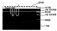
- Figure 4 shows the results of analyzing the elemental composition on the surface of the metal particle layer including the concave-convex structure formed according to the embodiment using a field emission scanning electron microscope (FE-SEM). Referring to FIG. 4, it can be seen that an uneven structure including Pd is formed.
- FE-SEM field emission scanning electron microscope
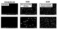
- FIG. 5 is an SEM image of the surface of the ITO substrate and the metal particle layer prepared in Examples and Comparative Examples after pretreatment. It can be seen from FIG. 5 that the metal particle layer in the case of using the organic acid according to the embodiment of the present invention has a smaller size and a higher density of the metal particles than in the case of the comparative example using the inorganic acid. In addition, it was also found that the surface of the ITO substrate was etched in the comparative example, so that Pd metal particles were not easily produced.
- the metal particle layer formed by the method according to the present invention forms a uniform nanoparticle layer, light extraction efficiency of 20% or more can be expected to be increased when a light emitting device is applied, and a small efficiency reduction of 5% or less can be expected even when a high power device is operated. Can be.
- the metal compound layer is reduced by a wet process of contacting the metal compound with an activation solution containing an organic acid activator to precipitate metal particles, thereby forming a metal particle layer having an uneven structure.
- the metal particle layer according to the present invention is applied to a light emitting device, the light extraction efficiency of the light emitting device can be improved by a simpler process.
Landscapes
- Electroluminescent Light Sources (AREA)
Abstract
Description
Claims (19)
- 산화되어 전자를 발생할 수 있는 기재를,금속화합물, 유기산 활성화제 및 착화제를 포함하는 활성화 용액과 접촉시키는 단계를 포함하며,상기 기재는 상기 유기산 활성화제에 의해 산화되어 전자를 발생시키고,상기 금속화합물은 상기 전자에 의해 환원되어 상기 기재의 표면 상에 금속입자로 석출되어 금속입자층을 형성하는 것인, 금속입자층 형성 방법.
- 제1항에 있어서,상기 금속입자층은 나노 크기의 요철 구조를 갖는 것인 방법.
- 제2항에 있어서, 상기 요철은 10 내지 1,000nm의 높이를 갖는 것인 방법.
- 제1항에 있어서,상기 기재는 인듐, 주석, 아연, 알루미늄, 갈륨, 안티몬, 이리듐, 루테늄, 니켈, 은, 금으로 이루어진 군에서 선택되는 하나 이상을 포함하는 것인 방법.
- 제4항에 있어서,상기 기재는 ITO(indium tin oxide), IZO(indium zinc oxide), IZTO(indium zinc tin oxide), IAZO(indium aluminum zinc oxide), IGZO(indium gallium zinc oxide), IGTO(indium gallium tin oxide), AZO(aluminum zinc oxide), ATO(antimony tin oxide), GZO(gallium zinc oxide), IrOx, RuOx, Ni, Ag 및 Au 로 이루어진 군에서 선택되는 어느 하나 이상을 포함하는 것인 방법.
- 제1항에 있어서,상기 금속입자층을 형성하기 이전에 상기 기재가 공기 중의 산소와 만나 형성되는 금속산화막을 제거하는 단계를 더 포함하는 방법.
- 제1항에 있어서,상기 금속입자층을 형성하는 단계는 상기 기재를 상기 활성화 용액에 1회 이상 침지하여 수행되는 것인 방법.
- 제1항에 있어서,상기 금속화합물은 팔라듐, 은, 금, 구리, 갈륨, 티타늄, 탄탈륨, 루테늄, 주석, 백금 또는 이들의 합금을 포함하는 금속염, 금속 산화물 및 금속 수화물로 이루어진 군에서 선택되는 어느 하나 이상을 포함하는 것인 방법.
- 제1항에 있어서,상기 활성화 용액 중 금속화합물의 농도는 0.001 내지 5g/L인 방법.
- 제1항에 있어서,상기 유기산 활성화제는 탄소수 1 ~ 10 의 유기산인 방법.
- 제1항에 있어서,상기 유기산 활성화제는 구연산(citric acid), 옥살산(oxalic acid), 말론산(malonic acid), 사과산(malic acid), 주석산(tartaric acid), 초산(acetic acid), 푸마르산(fumaric acid), 젖산(lactic acid), 포름산(formic acid), 프로피온산(propionic acid), 부티르산(butyric acid), 이미노디아세트산(iminodiacetic acid), 글리옥실산(glyoxylic acid) 및 아스코르빈산(ascorbic acid)으로 이루어진 군에서 선택되는 어느 하나 이상을 포함하는 것인 방법.
- 제1항에 있어서,상기 유기산 활성화제는 탄소수 2 내지 10 의 지방족 폴리카르본산(aliphatic polycarboxylic acid) 인 방법.
- 제1항에 있어서,상기 착화제는 HCl, HF, 및 NHF3으로 이루어진 군에서 선택되는 어느 하나 이상을 포함하는 것인 방법.
- 제1항에 있어서, 상기 활성화 용액은 알킬렌글리콜 모노알킬 에테르를 더 포함하는 것인 방법.
- 제1항 내지 제14항 중 어느 한 항에 따른 방법으로 제조된, 금속화합물의 환원에 의해 석출된 금속입자로 이루어진 금속입자층을 포함하는 소자.
- 기판 상에 발광 구조물, 전극층 및 금속입자층이 순차적으로 형성되어 있는 발광소자이며, 상기 금속입자층은 제1항 내지 제14항 중 어느 한 항에 따른 방법으로 금속화합물의 환원에 의해 석출된 금속 입자로 형성된 것인 발광소자.
- 제16항에 있어서,상기 발광 구조물은 n형 반도체층/활성층/p형 반도체층이 순차적으로 적층된 구조를 갖는 것인 발광소자.
- 제16항에 있어서,상기 전극층은 ITO(indium tin oxide), IZO(indium zinc oxide), IZTO(indium zinc tin oxide), IAZO(indium aluminum zinc oxide), IGZO(indium gallium zinc oxide), IGTO(indium gallium tin oxide), AZO(aluminum zinc oxide), ATO(antimony tin oxide), GZO(gallium zinc oxide), IrOx, RuOx, Ni, Ag 및 Au 로 이루어진 군에서 선택되는 어느 하나 이상을 이용하여 형성된 것인 발광소자.
- 제16항에 있어서, 상기 발광소자는 저출력용 발광 다이오드, 고출력 플립형 발광 다이오드, 수직형 발광 다이오드, 또는 유기 발광 다이오드인 발광소자.
Priority Applications (3)
| Application Number | Priority Date | Filing Date | Title |
|---|---|---|---|
| CN201380037834.3A CN104769733B (zh) | 2012-07-24 | 2013-07-22 | 用于改进发光器件的光提取效率的方法以及用于制造发光器件的方法 |
| US14/405,113 US10161046B2 (en) | 2012-07-24 | 2013-07-22 | Method for forming metal particle layer and light emitting device fabricated using metal particle layer formed by the method |
| JP2015501606A JP5876189B2 (ja) | 2012-07-24 | 2013-07-22 | 金属粒子層の形成方法、及び、発光素子の製造方法 |
Applications Claiming Priority (4)
| Application Number | Priority Date | Filing Date | Title |
|---|---|---|---|
| KR10-2012-0080457 | 2012-07-24 | ||
| KR20120080457 | 2012-07-24 | ||
| KR1020130086065A KR101548420B1 (ko) | 2012-07-24 | 2013-07-22 | 금속입자층 형성 방법 및 이를 이용하여 제조된 발광소자 |
| KR10-2013-0086065 | 2013-07-22 |
Publications (1)
| Publication Number | Publication Date |
|---|---|
| WO2014017793A1 true WO2014017793A1 (ko) | 2014-01-30 |
Family
ID=49997543
Family Applications (1)
| Application Number | Title | Priority Date | Filing Date |
|---|---|---|---|
| PCT/KR2013/006540 Ceased WO2014017793A1 (ko) | 2012-07-24 | 2013-07-22 | 금속입자층 형성 방법 및 이를 이용하여 제조된 발광소자 |
Country Status (1)
| Country | Link |
|---|---|
| WO (1) | WO2014017793A1 (ko) |
Cited By (1)
| Publication number | Priority date | Publication date | Assignee | Title |
|---|---|---|---|---|
| CN112186081A (zh) * | 2020-09-28 | 2021-01-05 | 华灿光电(苏州)有限公司 | 发光二极管外延片及其制备方法 |
Citations (5)
| Publication number | Priority date | Publication date | Assignee | Title |
|---|---|---|---|---|
| US20080105560A1 (en) * | 2006-11-08 | 2008-05-08 | Industrial Technology Research Institute | Method for Preparing Nano Metallic Particles |
| US20080303034A1 (en) * | 2007-06-08 | 2008-12-11 | Kuo-Chin Huang | Light-emitting gallium nitride-based III-V group compound semiconductor device and manufacturing method thereof |
| US7776196B2 (en) * | 2006-09-28 | 2010-08-17 | Kabushiki Kaisha Toshiba | Method for arranging particles and method for manufacturing light-emitting device |
| KR20120014677A (ko) * | 2010-08-10 | 2012-02-20 | 인하대학교 산학협력단 | 전도성 매개물층이 적용된 금속 나노입자 내장형 발광다이오드 구조 |
| KR101134191B1 (ko) * | 2010-04-26 | 2012-04-09 | 전북대학교산학협력단 | 코어-쉘 나노입자를 이용한 표면 플라즈몬 공명-기반 발광 다이오드 |
-
2013
- 2013-07-22 WO PCT/KR2013/006540 patent/WO2014017793A1/ko not_active Ceased
Patent Citations (5)
| Publication number | Priority date | Publication date | Assignee | Title |
|---|---|---|---|---|
| US7776196B2 (en) * | 2006-09-28 | 2010-08-17 | Kabushiki Kaisha Toshiba | Method for arranging particles and method for manufacturing light-emitting device |
| US20080105560A1 (en) * | 2006-11-08 | 2008-05-08 | Industrial Technology Research Institute | Method for Preparing Nano Metallic Particles |
| US20080303034A1 (en) * | 2007-06-08 | 2008-12-11 | Kuo-Chin Huang | Light-emitting gallium nitride-based III-V group compound semiconductor device and manufacturing method thereof |
| KR101134191B1 (ko) * | 2010-04-26 | 2012-04-09 | 전북대학교산학협력단 | 코어-쉘 나노입자를 이용한 표면 플라즈몬 공명-기반 발광 다이오드 |
| KR20120014677A (ko) * | 2010-08-10 | 2012-02-20 | 인하대학교 산학협력단 | 전도성 매개물층이 적용된 금속 나노입자 내장형 발광다이오드 구조 |
Cited By (2)
| Publication number | Priority date | Publication date | Assignee | Title |
|---|---|---|---|---|
| CN112186081A (zh) * | 2020-09-28 | 2021-01-05 | 华灿光电(苏州)有限公司 | 发光二极管外延片及其制备方法 |
| CN112186081B (zh) * | 2020-09-28 | 2021-08-03 | 华灿光电(苏州)有限公司 | 发光二极管外延片及其制备方法 |
Similar Documents
| Publication | Publication Date | Title |
|---|---|---|
| TWI362123B (ko) | ||
| CN106098882B (zh) | 一种发光二极管外延片及其制备方法 | |
| WO2009123401A1 (ko) | 발광소자 및 그 제조방법 | |
| CN101188263B (zh) | 氮化物半导体发光器件的制造方法 | |
| WO2014104621A1 (en) | Process for depositing epitaxial zno on iii-nitride-based light emitting diode and light emitting diode including epitaxial zno | |
| WO2009131401A2 (ko) | 발광 소자 및 그 제조방법 | |
| WO2010101332A1 (ko) | 발광소자 | |
| WO2017057997A1 (en) | Light emitting diode devices with zinc oxide layer | |
| JP5112761B2 (ja) | 化合物半導体素子およびそれを用いる照明装置ならびに化合物半導体素子の製造方法 | |
| CN103647009A (zh) | 氮化物发光二极管及其制备方法 | |
| WO2009126010A2 (ko) | 발광 소자 | |
| CN107482095B (zh) | 一种led外延生长方法 | |
| WO2010055987A1 (ko) | 산화갈륨 기반 기판 제조방법, 발광소자 및 발광소자 제조방법 | |
| CN114883460A (zh) | 发光二极管外延片及其制备方法 | |
| WO2013100619A1 (ko) | 탄소 도핑된 p형 질화물층을 포함하는 질화물계 발광소자 | |
| JP5638543B2 (ja) | 発光素子の製造方法 | |
| TWI488333B (zh) | LED element and manufacturing method thereof | |
| CN102044606A (zh) | 一种led外延片及其外延生长方法 | |
| KR101548420B1 (ko) | 금속입자층 형성 방법 및 이를 이용하여 제조된 발광소자 | |
| WO2013157875A1 (ko) | 고효율 발광다이오드 제조방법 | |
| KR100621918B1 (ko) | 투명 전도성 나노막대를 전극으로 포함하는 발광소자 | |
| WO2009134109A2 (ko) | 발광 소자 및 그 제조방법 | |
| WO2014017793A1 (ko) | 금속입자층 형성 방법 및 이를 이용하여 제조된 발광소자 | |
| WO2013066088A1 (ko) | 투명 박막, 이를 포함하는 발광 소자와 이들의 제조 방법 | |
| CN114094001B (zh) | 基底、发光二极管外延片及其制造方法 |
Legal Events
| Date | Code | Title | Description |
|---|---|---|---|
| 121 | Ep: the epo has been informed by wipo that ep was designated in this application |
Ref document number: 13823145 Country of ref document: EP Kind code of ref document: A1 |
|
| ENP | Entry into the national phase |
Ref document number: 2015501606 Country of ref document: JP Kind code of ref document: A |
|
| WWE | Wipo information: entry into national phase |
Ref document number: 14405113 Country of ref document: US |
|
| NENP | Non-entry into the national phase |
Ref country code: DE |
|
| 122 | Ep: pct application non-entry in european phase |
Ref document number: 13823145 Country of ref document: EP Kind code of ref document: A1 |