WO2014017159A1 - モジュールおよびその製造方法 - Google Patents
モジュールおよびその製造方法 Download PDFInfo
- Publication number
- WO2014017159A1 WO2014017159A1 PCT/JP2013/064617 JP2013064617W WO2014017159A1 WO 2014017159 A1 WO2014017159 A1 WO 2014017159A1 JP 2013064617 W JP2013064617 W JP 2013064617W WO 2014017159 A1 WO2014017159 A1 WO 2014017159A1
- Authority
- WO
- WIPO (PCT)
- Prior art keywords
- semiconductor substrate
- module
- resin layer
- main surface
- connection terminal
- Prior art date
- Legal status (The legal status is an assumption and is not a legal conclusion. Google has not performed a legal analysis and makes no representation as to the accuracy of the status listed.)
- Ceased
Links
Images


Classifications
-
- H—ELECTRICITY
- H10—SEMICONDUCTOR DEVICES; ELECTRIC SOLID-STATE DEVICES NOT OTHERWISE PROVIDED FOR
- H10W—GENERIC PACKAGES, INTERCONNECTIONS, CONNECTORS OR OTHER CONSTRUCTIONAL DETAILS OF DEVICES COVERED BY CLASS H10
- H10W74/00—Encapsulations, e.g. protective coatings
- H10W74/01—Manufacture or treatment
- H10W74/012—Manufacture or treatment of encapsulations on active surfaces of flip-chip devices, e.g. forming underfills
-
- H—ELECTRICITY
- H10—SEMICONDUCTOR DEVICES; ELECTRIC SOLID-STATE DEVICES NOT OTHERWISE PROVIDED FOR
- H10W—GENERIC PACKAGES, INTERCONNECTIONS, CONNECTORS OR OTHER CONSTRUCTIONAL DETAILS OF DEVICES COVERED BY CLASS H10
- H10W74/00—Encapsulations, e.g. protective coatings
- H10W74/01—Manufacture or treatment
- H10W74/014—Manufacture or treatment using batch processing
-
- H—ELECTRICITY
- H10—SEMICONDUCTOR DEVICES; ELECTRIC SOLID-STATE DEVICES NOT OTHERWISE PROVIDED FOR
- H10W—GENERIC PACKAGES, INTERCONNECTIONS, CONNECTORS OR OTHER CONSTRUCTIONAL DETAILS OF DEVICES COVERED BY CLASS H10
- H10W74/00—Encapsulations, e.g. protective coatings
- H10W74/10—Encapsulations, e.g. protective coatings characterised by their shape or disposition
- H10W74/111—Encapsulations, e.g. protective coatings characterised by their shape or disposition the semiconductor body being completely enclosed
- H10W74/114—Encapsulations, e.g. protective coatings characterised by their shape or disposition the semiconductor body being completely enclosed by a substrate and the encapsulations
- H10W74/117—Encapsulations, e.g. protective coatings characterised by their shape or disposition the semiconductor body being completely enclosed by a substrate and the encapsulations the substrate having spherical bumps for external connection
-
- H—ELECTRICITY
- H10—SEMICONDUCTOR DEVICES; ELECTRIC SOLID-STATE DEVICES NOT OTHERWISE PROVIDED FOR
- H10W—GENERIC PACKAGES, INTERCONNECTIONS, CONNECTORS OR OTHER CONSTRUCTIONAL DETAILS OF DEVICES COVERED BY CLASS H10
- H10W74/00—Encapsulations, e.g. protective coatings
- H10W74/10—Encapsulations, e.g. protective coatings characterised by their shape or disposition
- H10W74/15—Encapsulations, e.g. protective coatings characterised by their shape or disposition on active surfaces of flip-chip devices, e.g. underfills
-
- H—ELECTRICITY
- H10—SEMICONDUCTOR DEVICES; ELECTRIC SOLID-STATE DEVICES NOT OTHERWISE PROVIDED FOR
- H10W—GENERIC PACKAGES, INTERCONNECTIONS, CONNECTORS OR OTHER CONSTRUCTIONAL DETAILS OF DEVICES COVERED BY CLASS H10
- H10W90/00—Package configurations
- H10W90/701—Package configurations characterised by the relative positions of pads or connectors relative to package parts
-
- H—ELECTRICITY
- H10—SEMICONDUCTOR DEVICES; ELECTRIC SOLID-STATE DEVICES NOT OTHERWISE PROVIDED FOR
- H10W—GENERIC PACKAGES, INTERCONNECTIONS, CONNECTORS OR OTHER CONSTRUCTIONAL DETAILS OF DEVICES COVERED BY CLASS H10
- H10W72/00—Interconnections or connectors in packages
- H10W72/071—Connecting or disconnecting
- H10W72/072—Connecting or disconnecting of bump connectors
-
- H—ELECTRICITY
- H10—SEMICONDUCTOR DEVICES; ELECTRIC SOLID-STATE DEVICES NOT OTHERWISE PROVIDED FOR
- H10W—GENERIC PACKAGES, INTERCONNECTIONS, CONNECTORS OR OTHER CONSTRUCTIONAL DETAILS OF DEVICES COVERED BY CLASS H10
- H10W72/00—Interconnections or connectors in packages
- H10W72/071—Connecting or disconnecting
- H10W72/073—Connecting or disconnecting of die-attach connectors
-
- H—ELECTRICITY
- H10—SEMICONDUCTOR DEVICES; ELECTRIC SOLID-STATE DEVICES NOT OTHERWISE PROVIDED FOR
- H10W—GENERIC PACKAGES, INTERCONNECTIONS, CONNECTORS OR OTHER CONSTRUCTIONAL DETAILS OF DEVICES COVERED BY CLASS H10
- H10W72/00—Interconnections or connectors in packages
- H10W72/851—Dispositions of multiple connectors or interconnections
- H10W72/874—On different surfaces
- H10W72/877—Bump connectors and die-attach connectors
-
- H—ELECTRICITY
- H10—SEMICONDUCTOR DEVICES; ELECTRIC SOLID-STATE DEVICES NOT OTHERWISE PROVIDED FOR
- H10W—GENERIC PACKAGES, INTERCONNECTIONS, CONNECTORS OR OTHER CONSTRUCTIONAL DETAILS OF DEVICES COVERED BY CLASS H10
- H10W74/00—Encapsulations, e.g. protective coatings
- H10W74/10—Encapsulations, e.g. protective coatings characterised by their shape or disposition
- H10W74/131—Encapsulations, e.g. protective coatings characterised by their shape or disposition the semiconductor body being only partially enclosed
- H10W74/142—Encapsulations, e.g. protective coatings characterised by their shape or disposition the semiconductor body being only partially enclosed the encapsulations exposing the passive side of the semiconductor body
-
- H—ELECTRICITY
- H10—SEMICONDUCTOR DEVICES; ELECTRIC SOLID-STATE DEVICES NOT OTHERWISE PROVIDED FOR
- H10W—GENERIC PACKAGES, INTERCONNECTIONS, CONNECTORS OR OTHER CONSTRUCTIONAL DETAILS OF DEVICES COVERED BY CLASS H10
- H10W90/00—Package configurations
- H10W90/701—Package configurations characterised by the relative positions of pads or connectors relative to package parts
- H10W90/721—Package configurations characterised by the relative positions of pads or connectors relative to package parts of bump connectors
- H10W90/724—Package configurations characterised by the relative positions of pads or connectors relative to package parts of bump connectors between a chip and a stacked insulating package substrate, interposer or RDL
-
- H—ELECTRICITY
- H10—SEMICONDUCTOR DEVICES; ELECTRIC SOLID-STATE DEVICES NOT OTHERWISE PROVIDED FOR
- H10W—GENERIC PACKAGES, INTERCONNECTIONS, CONNECTORS OR OTHER CONSTRUCTIONAL DETAILS OF DEVICES COVERED BY CLASS H10
- H10W90/00—Package configurations
- H10W90/701—Package configurations characterised by the relative positions of pads or connectors relative to package parts
- H10W90/731—Package configurations characterised by the relative positions of pads or connectors relative to package parts of die-attach connectors
- H10W90/734—Package configurations characterised by the relative positions of pads or connectors relative to package parts of die-attach connectors between a chip and a stacked insulating package substrate, interposer or RDL
Definitions
- the present invention relates to a module in which a semiconductor substrate and connection terminals are arranged on one main surface of a wiring board, and a method for manufacturing the module.
- the semiconductor substrate 102 is flip-chip mounted, and the resin layer 104 covering the semiconductor substrate 102 and the connection terminals 103 is further formed. . Then, the module 100 is formed by polishing the resin layer 104 and the upper surface of the semiconductor substrate 102 so that the end surface of the connection terminal 103 is exposed from the upper surface of the resin layer 104.
- the semiconductor substrate 102 to be flip-chip mounted has a circuit formed on the surface facing the wiring substrate 101, and the upper surface of the semiconductor substrate 102 (the surface not facing the wiring substrate) is polished so that the characteristics of the semiconductor substrate 102 can be obtained. Therefore, the module 100 can be reduced in height by polishing the resin layer 104 and the semiconductor substrate 102 until the end face of the connection terminal 103 is exposed. Further, since the upper surface of the semiconductor substrate 102 having a higher thermal conductivity than the resin of the resin layer 104 is exposed from the surface of the resin layer 104, the heat dissipation characteristics of the module 100 are also improved.
- JP 2002-343904 (see paragraph 0013, FIG. 1, etc.)
- the present invention has been made in view of the above-described problems, and an object thereof is to provide a module having excellent heat dissipation characteristics and a method for manufacturing the module.
- a module of the present invention includes a wiring board, a semiconductor substrate mounted on one main surface of the wiring board, and provided on the one main surface, on one side of the semiconductor substrate. And a resin layer covering a part of the side surface of the semiconductor substrate so that the end portion is exposed.
- a columnar connection terminal may be erected on the one main surface of the wiring board such that one end thereof is exposed from the resin layer.
- the module can be connected to an external mother board or the like by the connection terminal.
- the connection terminal having a high thermal conductivity is exposed from the surface of the resin layer, the heat generated from the module can be dissipated from the connection terminal, thereby further improving the heat dissipation characteristics of the module.
- connection terminal since the side surface of the connection terminal is exposed from the surface of the resin layer, when connecting the module and the mother board with solder, the solder forms a fillet shape in a state of spreading to the side surface of the connection terminal.
- the connection strength with the mother board is improved.
- the height of the end surface on the one end side of the connection terminal from the one main surface of the wiring board is higher than the height of the end surface on the one surface side of the semiconductor substrate from the one main surface. You may do it. In this way, when the module is connected to an external mother board or the like, the module and the mother board can be easily connected without interfering with the semiconductor substrate.
- the height of the end surface on the one surface side of the semiconductor substrate from the one main surface of the wiring substrate is higher than the height from the one main surface of the end surface on the one end portion side of the connection terminal. You may do it.
- the distance between one surface of the semiconductor substrate and the mother board is shortened, so that the heat generated from the module passes through the planar ground electrode or the like formed on the mother board. Heat dissipation, and the heat dissipation characteristics of the module are improved.
- the distance between the mother board and the connection terminal is larger than the distance between the mother board and the semiconductor substrate, so a gap is formed between the mother board and the connection terminal. can do.
- the solder that connects the mother board and the connection terminal is not pressed down, and the solder does not easily protrude from the connection portion, so that a short circuit between the solder and the adjacent terminal (for example, the adjacent connection terminal) is prevented. be able to.
- a contact portion of the surface of the resin layer with the semiconductor substrate is formed in a fillet shape that spreads from the edge of the side surface of the semiconductor substrate toward the resin layer. In this way, the stress applied to the contact portion between the surface of the resin layer and the semiconductor substrate is dispersed by the resin formed in a fillet shape, so that the resin of the resin layer can be prevented from peeling from the semiconductor substrate.
- corner portion of the semiconductor substrate protruding from the surface of the resin layer may be chamfered.
- irregularities may be formed on the one surface of the semiconductor substrate. If unevenness is formed on one surface of the semiconductor substrate exposed from the resin layer, the surface area (exposed portion) of the semiconductor substrate having a high thermal conductivity increases, so that the heat dissipation characteristics can be further improved.
- a metal film may be formed on at least a part of the one surface of the semiconductor substrate exposed from the resin layer.
- the heat dissipation characteristics of the module are further improved by the metal film having a higher thermal conductivity than the semiconductor substrate.
- the metal film as an electrode for connection with an external mother board, etc., the module and the mother board can be connected with the connection terminal and the metal film. The connection strength can be improved.
- irregularities may be formed on the surface of the metal film.
- the surface area of the metal film is increased, the heat dissipation characteristics of the module are further improved.
- the connection area increases, so that the connection strength between the module and the mother board can be improved.
- a module manufacturing method includes: a module body including a wiring substrate, a semiconductor substrate mounted on one main surface of the wiring substrate, and a resin layer provided on the one main surface that covers the semiconductor substrate.
- a resin layer covering a part of the side surface of the semiconductor substrate can be formed so that the end portion on the one surface side of the semiconductor substrate is exposed, so that the heat dissipation characteristics are excellent. Modules can be manufactured.
- the module element body further provided with a columnar connection terminal erected on the one main surface of the wiring board covered with the resin layer is prepared, and in the removal step, You may make it remove a part of said resin layer so that the edge part of the said one surface side of a semiconductor substrate and the one edge part of the said connection terminal may be exposed.
- the height of the end surface on the one end side of the connection terminal from the one main surface of the wiring board is set to the height from the one main surface of the end surface on the one surface side of the semiconductor substrate.
- the module may be manufactured to be higher than the height. In this way, a module that can be easily connected to an external mother board can be manufactured.
- the height of the end surface on the one surface side of the semiconductor substrate from the one main surface of the wiring substrate is set from the one main surface of the end surface on the one end portion side of the connection terminal.
- the module may be manufactured to be higher than the height. In this way, when the mother board and the module (connection terminal) are connected, the distance between the mother board and the semiconductor substrate is shortened, so that the heat generated from the module is transmitted via the ground electrode of the mother board and the like. A module that can easily dissipate heat can be manufactured.
- the distance between the mother substrate and the connection terminal is larger than the distance between the mother substrate and the semiconductor substrate, a gap can be formed between the mother substrate and the connection terminal. In this way, the solder that joins the mother board and the connection terminal is not pressed down, and the solder hardly protrudes from the joined portion, so that a module that can prevent a short circuit with the adjacent terminal can be manufactured.
- the resin layer that covers a part of the side surface of each of the semiconductor substrate and the connection terminal is formed so that the end portion on the one surface side of the semiconductor substrate disposed on the one main surface of the wiring substrate is exposed.
- FIG. 1 is a cut front view of the module mounting apparatus 1 on which the module 2 is mounted.
- a module mounting apparatus 1 on which a module 2 according to this embodiment is mounted includes a mother board 3, a module 2 mounted on the mother board 3, and a connecting portion between the mother board 3 and the module 2. And an underfill resin layer 4 made of a resin, for example, and mounted on an electronic device using a high frequency such as a mobile phone.
- the mother board 3 has a ground electrode 5 for grounding and wiring patterns (not shown) constituting various circuits, and the ground electrode 5 and the wiring pattern are formed in a predetermined wiring pattern or mother board 3 by a via conductor 6 or the like. Are connected to the mounting electrodes 7 formed on the front and back surfaces.
- the ground electrode 5 formed on the mother substrate 3 is connected to the mounting electrode 7 connected to the columnar connection terminal 8 of the module 2 described later and the metal film 10 formed on the lower surface 9a of the semiconductor substrate 9. It is connected via a conductor 6.
- the mother substrate 3 is formed of a material such as glass epoxy resin or ceramic.
- the underfill resin layer 4 is made of, for example, an epoxy resin, and is formed by filling a resin so as to fill a gap between the mother substrate 3 and the module 2 when the module 2 is mounted on the mother substrate 3.
- the underfill resin layer 4 may be omitted.
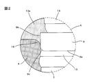
- FIG. 2 is an enlarged view of area A in FIG.
- the module 2 includes a wiring board 11, a semiconductor substrate 9 mounted on one main surface 11 a of the wiring board 11, a column-shaped connection terminal 8 erected, and the other main board 11 of the wiring board 11.
- Chip components 12a, 12b, and 12c mounted on the surface 11b, a resin layer 13a that covers the semiconductor substrate 9 and the connection terminals 8 on one main surface 11a of the wiring substrate 11, and a chip component on the other main surface 11b of the wiring substrate 11 And a resin layer 13b covering 12a to 12c.
- the module include a Bluetooth (registered trademark) module, a wireless LAN module, and an antenna switch module disposed immediately below an antenna of a mobile phone.
- the wiring substrate 11 is formed of a glass epoxy resin substrate, a low-temperature co-fired ceramic (LTCC) substrate, a glass substrate, and the like, and both main surfaces 11a and 11b have mounting electrodes 15 and electrodes 15a for forming connection terminals 8; A wiring pattern (not shown) and the like are formed, and a ground electrode 14 for grounding, another wiring pattern (not shown), a via conductor (not shown) and the like are formed inside.
- the wiring board 11 may be either a single layer board or a multilayer board.
- the wiring substrate 11 is an LTCC multilayer substrate
- a ceramic green sheet in which a slurry in which a mixed powder such as alumina and glass is mixed with an organic binder and a solvent is formed into a sheet is formed.
- Via holes are formed at predetermined positions of the ceramic green sheet by laser processing, etc., and the formed via holes are filled with a conductor paste containing Ag, Cu, etc., and via conductors for interlayer connection are formed, and printing by the conductor paste is performed.
- Various electrode patterns are formed. Thereafter, the ceramic green sheets are laminated and pressed to form a ceramic laminate, which is fired at a low temperature of about 1000 ° C., so-called low temperature firing.
- the semiconductor substrate 9 and the chip components 12a to 12c are mounted on both the main surfaces 11a and 11b of the wiring substrate 11 as mounting components.
- the semiconductor substrate 9 forms a system IC that processes, for example, an RF signal and a baseband signal by forming a predetermined electric circuit on the surface of the wiring substrate 11 that faces the one main surface 11a.
- face down mounting flip chip mounting
- the chip components 12a to 12c are composed of a chip capacitor, a chip inductor, and a chip resistor, and are mounted on the other main surface 11b of the wiring board 11 by a known surface mounting technique.
- the columnar (pin-shaped) connection terminals 8 are mainly composed of Cu, for example, and are mounted on the electrodes 15a formed on one main surface of the wiring board 11 via solder.
- a metal film 10 is formed on the lower surface 9 a (corresponding to one surface in the present invention) of the semiconductor substrate 9 and the lower end surface 8 a of the connection terminal 8.
- the metal film 10 is, for example, a Ni / Au film in which a Ni layer is formed on the lower surface 9a of the semiconductor substrate 9 (or the lower end surface 8a of the connection terminal 8), and an Au layer is formed on the Ni layer. .
- the chip components 12a to 12c mounted on the other main surface 11b of the wiring board 11 there are some chip components 12a to 12c that are different in height from the other main surface 11b of the wiring board 11, In this embodiment, as shown in FIG. 1, the chip component 12a has the lowest height from the other main surface 11b of the wiring board 11 among all the chip components 12a to 12c. Further, each of the semiconductor substrate 9 and the connection terminal 8 is formed so that the height from the one main surface 11a of the wiring substrate 11 is the same in the mounted or standing state.
- the height Ht of the semiconductor substrate 9 (or connection terminal 8) having the highest height from the one main surface 11a of the wiring substrate 11 on the one main surface 11a of the wiring substrate 11 is the other main surface of the wiring substrate 11.
- 11b of the chip component 12a that other from the main surface 11b of the height H 0 semiconductor substrate to be lower than the (other main surface tallest low chip component in 11b) 9 (or the connection terminal 8) is formed ing.
- the semiconductor substrate 9 has a larger area (cross-sectional area) than any of the other mounting components (each chip component 12a to 12c). .
- the height of the lower end surface 8a (one surface side end surface) of the connection terminal 8 from the one main surface 11a of the wiring substrate 11 is from the one main surface 11a of the lower surface 9a (one surface side end surface) of the semiconductor substrate 9.
- the connection terminals 8 may be formed so as to be higher than the height. By forming the connection terminals 8 in this way, the semiconductor substrate 9 does not get in the way when the module 2 is mounted on the external mother substrate 3, and the mountability of the module 2 is improved.
- the semiconductor substrate 9 is formed such that the height of the lower surface 9a of the semiconductor substrate 9 from the one main surface 11a of the wiring substrate 11 is higher than the height from the one main surface 11a of the lower end surface 8a of the connection terminal 8. It may be a configuration. In this case, when the module 2 is connected to the mother substrate 3, the distance between the lower surface 9 a of the semiconductor substrate 9 and the mother substrate 3 is shortened, so that the heat generated from the module 2 is formed on the surface of the mother substrate 3. It is easy to dissipate heat through the ground electrode 5 and the heat dissipation characteristics of the module 2 are improved.
- the distance between the mother board and the connection terminal 8 is larger than the distance between the mother board and the semiconductor substrate 9.
- a gap can be formed between the two.
- the solder that connects the mother board and the connection terminal 8 is not pressed down, and the solder does not easily protrude from the connection portion, so that it is possible to prevent a short circuit between the connection terminal 8 and another adjacent terminal. it can.
- the resin layer 13a on the one principal surface 11a of the wiring board 11 is made of, for example, epoxy resin, and as shown in FIG. 1, the end on the lower surface 9a side of the semiconductor substrate 9 and the lower end of the connection terminal 8 (one in the present invention). Part of the side surfaces of the semiconductor substrate 9 and the connection terminal 8 are formed so as to be exposed).
- the end portion on the lower surface 9 a side of the semiconductor substrate 9 is a portion including the lower surface 9 a of the semiconductor substrate 9 and part of the side surface adjacent to the lower surface 9 a of the semiconductor substrate 9. That is, the resin layer 13a is formed so that the lower end portion of the semiconductor substrate 9 and the lower end portion of the connection terminal 8 protrude from the surface of the resin layer 13a.
- the contact portion 16 of the surface of the resin layer 13a with the semiconductor substrate 9 is, as shown in FIG. 2, from the edge of the side surface 9b of the semiconductor substrate 9 toward the resin layer 13a from the lower edge of the semiconductor substrate 9. It is formed in a fillet shape spreading at the bottom. Further, the corner portion 9c of the portion protruding from the surface of the resin layer 13a of the semiconductor substrate 9 is chamfered. These shapes can be formed by a removing step for removing the resin described later.
- the resin layer 13b on the other main surface 11b of the wiring board 11 is made of, for example, the same kind of epoxy resin as the resin layer 13a on the one main surface 11a, so that the chip components 12a to 12c are not exposed as shown in FIG. It is formed in a state where all of the chip parts are covered.
- the resin forming the resin layer 13b is a resin to suppress the warp. It is preferable to use a resin having a smaller linear expansion coefficient than the resin forming the layer 13a.
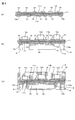
- FIGS. 3 shows a part of each process for manufacturing the module 2
- FIG. 4 shows each process following FIG.
- a planar grounding ground electrode 14 and a wiring pattern are formed therein, and the semiconductor substrate 9 and the chip components 12a to 12c are formed on both main surfaces 11a and 11b.
- the wiring board 11 on which the mounting electrode 15 and the connection terminal forming electrode 15a are formed is prepared (wiring board preparation step).
- the semiconductor substrate 9, the connection terminal 8, and the chip components 12a to 12c are mounted at positions corresponding to the mounting electrodes 15 of the wiring substrate 11 (component and connection terminal mounting).
- the semiconductor component 9 is face-down mounted (flip chip mounting) on the one main surface 11a of the wiring substrate 11, and the chip components 12a to 12c are mounted on the other main surface 11b of the wiring substrate 11 by a known surface mounting technique.
- the pin-like connection terminals 8 are mounted on the electrodes 15 for forming the connection terminals of the wiring board 11 via solder.
- the connection terminal 8 for example, a columnar metal made of Cu or an alloy containing Cu as a main component can be used.
- a resin layer 13a covering the semiconductor substrate 9 and the connection terminals 8 is formed on one main surface 11a of the wiring substrate 11, and each chip component is formed on the other main surface 11b.
- a resin layer 13b covering 12a to 12c is formed (resin layer forming step).
- a resin is applied or printed on both the main surfaces 11a and 11b by using a dispensing method or a printing method, and put into an oven set at a predetermined curing temperature (for example, about 180 ° C. for an epoxy resin). For example, the resin is cured to form both resin layers 13a and 13b.
- the semiconductor substrate 9 and the columnar connection terminals 8 mounted on the one main surface 11a of the wiring substrate 11 and the semiconductor substrate 9 and the connection terminals 8 provided on the one main surface 11a of the wiring substrate 11 are covered.
- a resin layer 13a, chip components 12a to 12c mounted on the other main surface 11b of the wiring substrate 11, and a resin layer 13b covering the chip components 12a to 12c provided on the other main surface 11b of the wiring substrate 11 The module body 18 provided is manufactured.
- connection terminal 8 can be easily mounted in the mounting process of the semiconductor substrate 9, but the method of forming the connection terminal 8 is the method described above.
- the columnar connection terminals 8 may be formed by plating before mounting the semiconductor substrate 9 on the one main surface 11a of the wiring substrate 11.
- the semiconductor substrate 9 is mounted after the connection terminal 8 is formed, and the resin layer 13a is formed by covering the connection terminal 8 with resin together with the semiconductor substrate 9 mounted on the one main surface 11a.
- the solder for connecting the connection terminal is exposed from the resin layer 13a as described above even if the connection terminal 8 is polished or ground. There is no. Therefore, the connection terminals 8 having a fine diameter can be formed with high precision on the one main surface 11a of the wiring board 11, and the pitch of the connection terminals 8 can be reduced.
- connection terminals 8 are formed after mounting the semiconductor substrate 9, the resin layer 13 a is formed before the connection terminals 8 are formed, and the surface of the connection terminal forming electrode 15 a is exposed by irradiating the surface of the resin layer 13 a with a laser.
- a recess for forming a connection terminal is formed in the resin layer 13a, and a conductive paste (for example, Ag paste or Cu paste) is filled in the recess by using a printing technique, or a conductor (for example, Cu) is formed by plating or the like.
- the columnar connection terminals 8 may be formed on the one main surface 11 a of the wiring substrate 11.
- wiring board preparation step to resin layer formation step correspond to the preparation step in the present invention.
- the surface of the resin layer 13a of the module body 18 is polished so that the lower surface 9a of the semiconductor substrate 9 and the lower end of the connection terminal 8 are exposed from the surface of the resin layer 13a. Or it grinds and removes a part (removal process).
- the resin of the resin layer 13a when the resin of the resin layer 13a is removed by polishing, it is preferably performed by lapping or sand blasting using loose abrasive grains. Since the resin of the resin layer 13a can be removed preferentially by adjusting the particle size, material, etc. of the loose abrasive grains, the end on the lower surface 9a side of the semiconductor substrate 9 and the lower end of the connection terminal 8 are exposed. As described above, it is possible to easily form the resin layer 13a that covers part of the side surfaces of the semiconductor substrate 9 and the connection terminal 8. In this step, the semiconductor substrate 9 and part of the lower end portion of the connection terminal 8 may be removed.
- the corner portion 9c of the portion protruding from the surface of the resin layer 13a of the semiconductor substrate 9 is chamfered, and the contact portion 16 between the surface of the resin layer 13a and the semiconductor substrate 9 (side surface 9b) 9 is formed in a fillet shape spreading toward the resin layer 13a from the edge of the side surface 9b on the lower surface 9a side of the semiconductor substrate 9 (see FIG. 2).
- angular part 9c does not need to be chamfered by adjusting the particle size, material, etc. of a loose abrasive grain, and the contact part 16 does not need to be made into a fillet shape.
- the lower surface 9a of the semiconductor substrate 9 is polished or ground so as to be uneven.
- the unevenness when unevenness is formed on the lower surface 9a of the semiconductor substrate 9, when the metal film 10 is formed on the lower surface 9a, the unevenness can be formed also on the metal film 10, and the thermal conductivity is high.
- the surface area of the metal film 10 can be increased.
- the unevenness formed on the lower surface 9a of the semiconductor substrate 9 may be formed with an average surface roughness (Ra) in the range of 0.1 ⁇ m to 15 ⁇ m. preferable.
- the terminal 8 is polished or ground.
- the height Ht of the semiconductor substrate 9 (or connection terminal 8) having the highest height from the one main surface 11a of the wiring substrate 11 is the chip component 12a having the lowest height from the other main surface 11b of the wiring substrate 11. polishing or grinding a semiconductor substrate 9 (or the connection terminal 8) to be lower than the height H 0 of the.
- the semiconductor substrate 9 and the connection terminal 8 may be polished or ground.
- the height of the semiconductor substrate 9 and the connection terminal 8 can be adjusted by adjusting the particle size, material, and the like of the loose abrasive used for polishing.
- a metal film 10 is formed on the lower surface 9a of the semiconductor substrate 9 and the lower end surface 8a of the connection terminal 8 exposed from the surface of the resin layer 13a (metal film forming step).
- Module 2 is manufactured.
- the metal film 10 is formed using a plating process or a printing technique.
- a plating process a Ni layer is grown on the lower surface 9a of the semiconductor substrate 9 and the lower end surface 8a of the connection terminal 8, and an Au layer is grown thereon to form the metal film 10.
- the metal film 10 on the lower surface 9a of the semiconductor substrate 9 does not need to be formed on the entire surface of the lower surface 9a of the semiconductor substrate 9, and may be formed at least partially.
- the lower surface 9a of the semiconductor substrate 9 is set so that the one main surface 11a of the wiring substrate 11 of the module 2 manufactured by the method for manufacturing the module 2 faces the mother substrate 3.
- the metal film 10 formed on the lower end surface 8a of the connection terminal 8 and the mounting electrode 7 formed on the surface of the mother substrate 3 are connected by soldering or the like.
- the metal substrate 10 is not formed on the semiconductor substrate 9 and the connection terminals 8. It is also possible to connect the module 2.
- the semiconductor substrate 9 and the connection terminals 8 that are flip-chip mounted are disposed on the one main surface 11a of the wiring substrate 11, and a chip such as a chip capacitor is disposed on the other main surface 11b.
- Parts 12a to 12c are arranged.
- the module 2 In order to reduce the size of the module 2 (to reduce the mounting area of the wiring board 11), it is effective to dispose mounting components on both main surfaces 11a and 11b of the wiring board 11. Further, as in the prior art shown in FIG. 5, it is also effective to reduce the height of the module 2 by reducing the height by polishing the lower surface 9 a of the semiconductor substrate 9 together with the connection terminals 8. However, for example, when the semiconductor substrate 9 and the chip components 12a to 12c are mounted on the same main surface of the wiring substrate 11, the lower surface 9a of the semiconductor substrate 9 is polished to reduce the height of the module 2. It is difficult.
- the flip-chip mounted semiconductor substrate 9 and the connection terminal 8 are disposed on the one main surface 11a of the wiring substrate 11 so that the characteristics are not deteriorated even when the lower surface 9a is polished.
- the chip parts 12a to 12b such as chip capacitors and chip inductors are arranged on the other main surface 11b, and the surface of the resin layer 13a on the one main surface 11a of the wiring board 11 is polished or ground together with the semiconductor substrate 9 and the connection terminals 8.
- the height Ht of the semiconductor substrate 9 (or connection terminal 8) having the highest height from the one main surface 11a of the wiring substrate 11 is the chip component 12a having the lowest height from the other main surface 11b of the wiring substrate 11.
- the height H 0 semiconductor substrate 9 to be lower than (or connecting terminals 8) is polished or ground, it is possible to reduce the height of reliably module 2.
- the module 2 is mounted on the mother substrate 3 as compared with the configuration of the module in which the lower surface 9a of the semiconductor substrate 9 is covered with the resin layer 13a.
- the distance between the lower surface 9a of the semiconductor substrate 9 and the planar ground electrode 5 formed on the mother substrate 3 is shortened, thereby improving the shielding characteristics of the semiconductor substrate 9.
- the heat generated from the module 2 is easily radiated through the ground electrode 5, so that the heat dissipation characteristics of the module 2 are improved. To do.
- connection terminal 8 connected to the ground electrode 5 of the mother board 3 (height from the one main surface 11a of the wiring board 11) can be shortened.
- the parasitic inductance due to the connection terminal 8 is reduced, and the ground can be strengthened.
- the amount of resin forming the resin layer 13a is less than the amount of resin in the resin layer 13b on the other main surface 11b.
- the semiconductor substrate 9 that is harder than the resin forming the both resin layers 13a and 13b has a wiring board 11 Of the mounting components 9, 12a to 12c mounted on both the main surfaces 11a and 11b, the one having the largest area (cross-sectional area) in plan view is used. Therefore, the shrinkage of both the resin layers 13a and 13b described above is used. Warpage of the wiring substrate 11 caused by the stress balance being lost can be suppressed.
- the resin forming the resin layer 13b has a smaller linear expansion coefficient than that of the resin forming the resin layer 13a, warping of the wiring board 11 can be further suppressed.
- a part of each side surface of the semiconductor substrate 9 and the connection terminal 8 is formed so that the end portion on the lower surface 9a side of the semiconductor substrate 9 and the lower end portion of the connection terminal 8 are exposed. Since the resin layer 13a to be coated is formed, the lower end portion including the lower surface 9a of the semiconductor substrate 9 having higher thermal conductivity than the resin of the resin layer 13a is exposed, so that only the lower surface 9a of the semiconductor substrate 9 is conventionally provided. As compared with the module in which is exposed, the heat dissipation characteristics of the module 2 can be improved.
- the contact portion 16 of the surface of the resin layer 13 a with the semiconductor substrate 9 is resin from the edge of the side surface 9 b of the semiconductor substrate 9 on the lower surface 9 a side of the semiconductor substrate 9. Since it is formed in a fillet shape spreading toward the bottom toward the layer 13a, the stress applied to the contact portion 16 between the surface of the resin layer 13a and the semiconductor substrate 9 is dispersed by the resin formed in the fillet shape, and the resin of the resin layer 13a Can be prevented from peeling from the semiconductor substrate 9.
- the unevenness is formed on the lower surface 9a of the semiconductor substrate 9, the surface area of the semiconductor substrate 9 having high thermal conductivity (the portion exposed from the resin layer 13a) increases, and the heat dissipation characteristics of the module 2 are improved.
- the metal film 10 is formed on at least a part of the lower surface 9a of the semiconductor substrate 9 exposed from the resin layer 13a, the metal film 10 having higher thermal conductivity than the semiconductor substrate 9 improves the heat dissipation characteristics of the module 2. To do. Further, by using the metal film 10 formed on the lower surface 9 a of the semiconductor substrate 9 as an electrode for connection with the mother substrate 3, the connection between the mother substrate 3 and the module 2 is connected to the connection terminal 8 and the metal film 10. Therefore, the connection strength between the mother board 3 and the module 2 can be improved.
- the surface area of the metal film 10 is increased, and the heat dissipation characteristics of the module 2 can be improved. Further, when the metal film 10 is used as an electrode for connection with the mother substrate 3, the connection area is increased, so that the connection strength between the module 2 and the mother substrate 3 can be improved.
- the metal film 10 is formed of a Ni / Au film, the wettability of solder when the module 2 and the mother board 3 are connected by solder is improved.
- the lower surface 9a of the semiconductor substrate 9 is protected by forming the metal film 10 on the lower surface 9a of the semiconductor substrate 9, it is possible to suppress the semiconductor substrate 9 from being damaged by external stress or the like.
- the area of the semiconductor substrate 9 in plan view may be smaller than the area of any of the other mounted components.
- it may be disposed on the one main surface 11a of the wiring substrate 11. That is, it is only necessary to mount or place the semiconductor substrate 9 whose lower surface 9a can be polished or ground on the one main surface 11a of the wiring substrate 11, and in order to reduce the mounting area of the wiring substrate 11, What is necessary is just to devise arrangement
- chip components 12a to 12c such as chip capacitors and chip inductors are mounted on the other main surface 11b of the wiring board 11, but the other main surface 11b is the same as the semiconductor substrate 9 mounted on the one main surface 11a.
- a different semiconductor substrate 9 may be mounted.
- connection terminals 8 formed on one main surface 11 a of the wiring board 11 may be any number, and the connection terminals 8 may be arranged on the other main surface 11 b of the wiring board 11. Further, the connection terminals 8 are not necessarily arranged on the one main surface 11 a of the wiring board 11. That is, the connection terminal 8 and the semiconductor substrate 9 may be disposed on different main surfaces of the wiring substrate 11.
- a shield layer made of a metal film may be formed on at least one of the resin layer 13a and the resin layer 13b.
- the resin layer 13b may not be provided.
- the present invention can be applied to various modules in which a semiconductor substrate and connection terminals are arranged on one main surface of a wiring board.
Landscapes
- Structures Or Materials For Encapsulating Or Coating Semiconductor Devices Or Solid State Devices (AREA)
Abstract
放熱特性の優れたモジュールとこのモジュールの製造方法を提供することを目的とする。 モジュール2は、配線基板11と、記配線基板11の一方主面11aに実装された半導体基板9と、一方主面11aに立設された柱状の接続端子8と、一方主面11aに設けられ、半導体基板9の下面9a側の端部と接続端子8の下端部が露出するように、半導体基板9および接続端子8それぞれの側面の一部を被覆する樹脂層13aとを備えることにより、樹脂層13aの樹脂よりも熱伝導率が高い半導体基板9の下面9a側の端部および接続端子8の下端部が樹脂層13aの表面から露出するため、放熱特性の優れたモジュール2を得ることができる。
Description
本発明は、配線基板の一方主面上に半導体基板と接続端子が配置されたモジュールおよびこのモジュールの製造方法に関する。
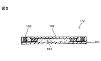
近年、携帯電話などの携帯端末装置の小型・薄型化に伴って、これに搭載されるモジュールの小型化が要求されている。そこで、従来では、図5に示すように、モジュール100を構成する配線基板101の一方主面上にフェイスダウンで実装(フリップチップ実装)された半導体基板102と、該半導体基板102と同一主面上に配置された柱状の接続端子103と、半導体基板102および柱状の接続端子103を被覆する樹脂層104を備えるモジュールが提案されている(特許文献1)。
この場合、モジュール100の一方主面上に柱状の接続端子103を形成した後、半導体基板102をフリップチップ実装し、さらに、当該半導体基板102および接続端子103を被覆する樹脂層104が形成される。そして、樹脂層104の上面から接続端子103の端面が露出するように、樹脂層104と半導体基板102の上面を研磨してモジュール100を形成する。
フリップチップ実装される半導体基板102は、配線基板101との対向面に回路が形成されており、半導体基板102の上面(配線基板との非対向面)を研磨することで、半導体基板102の特性を変えずにモジュール100の低背化が可能であるため、接続端子103の端面が露出するまで樹脂層104および半導体基板102を研磨することで、モジュール100の低背化が可能である。また、熱伝導率が樹脂層104の樹脂よりも高い半導体基板102の上面が樹脂層104の表面から露出するため、モジュール100の放熱特性も向上する。
しかしながら、上記した従来技術では、半導体基板102の上面のみが樹脂層104から露出しているため、発熱性が高い半導体基板(例えば、高周波モジュール等で使用されるパワーアンプIC等)を実装した場合に、放熱が足りずに、半導体基板102が誤動作する等の不具合が生じるおそれがあった。
本発明は、上記した課題に鑑みてなされたものであり、放熱特性の優れたモジュールを提供するとともに、このモジュールの製造方法を提供することを目的とする。
上記した目的を達成するために、本発明のモジュールは、配線基板と、前記配線基板の一方主面に実装された半導体基板と、前記一方主面に設けられ、前記半導体基板の一方面側の端部が露出するように、前記半導体基板の側面の一部を被覆する樹脂層とを備えたことを特徴としている。
このように構成することにより、樹脂層よりの熱伝導率が高い半導体基板の一方面のみならず側面の一部も樹脂層の表面から露出するため、半導体基板の一方面のみが樹脂層から露出する従来のモジュールと比較して、モジュールの放熱特性を向上することができる。
また、前記配線基板の前記一方主面に、その一方端部が前記樹脂層から露出するように柱状の接続端子が立設されていてもよい。このように構成することで、接続端子により、モジュールと外部のマザー基板等とを接続することが可能になる。また、熱伝導率の高い接続端子が樹脂層表面から露出するため、モジュールから発生する熱を接続端子からも放熱することができ、これにより、モジュールの放熱特性がさらに向上する。
また、接続端子の側面が樹脂層の表面から露出するため、モジュールとマザー基板とを半田により接続する際、半田が、接続端子の側面まで濡れ広がった状態のフィレット形状を形成するため、モジュールとマザー基板との接続強度が向上する。
また、前記接続端子の前記一方端部側の端面の前記配線基板の前記一方主面からの高さが、前記半導体基板の前記一方面側の端面の前記一方主面からの高さよりも高くなるようにしてもよい。このようにすることで、モジュールを外部のマザー基板等に接続する際、半導体基板が邪魔にならずに、モジュールとマザー基板との接続を容易に行うことができる。
また、前記半導体基板の前記一方面側の端面の前記配線基板の前記一方主面からの高さが、前記接続端子の前記一方端部側の端面の前記一方主面からの高さよりも高くなるようにしてもよい。この場合、モジュールをマザー基板等に接続したときに半導体基板の一方面とマザー基板との距離が短くなるため、モジュールから発生する熱が、マザー基板に形成された面状のグランド電極などを介して放熱しやすくなり、さらにモジュールの放熱特性が向上する。
また、マザー基板と接続端子とを半田により接続する際、マザー基板と接続端子との距離がマザー基板と半導体基板との距離よりも大きくなるため、マザー基板と接続端子との間にギャップを形成することができる。このようにすると、マザー基板と接続端子とを接続する半田が押さえつけられることがなく、半田が接続部分からはみ出しにくくなるため、半田と隣接端子(例えば、隣接した接続端子)との短絡を防止することができる。
また、前記樹脂層の表面の前記半導体基板との接触部が、前記半導体基板の側面の前記一方面側の端縁から樹脂層に向けて裾広がりのフィレット状に形成されていることが好ましい。このようにすると、樹脂層の表面と半導体基板との接触部にかかる応力がフィレット状に形成された樹脂により分散されるため、樹脂層の樹脂が半導体基板から剥離することを防止できる。
また、前記半導体基板の前記樹脂層の表面から突出した部分の角部が、面取りされていてもよい。このように構成することにより、半導体基板の割れや欠けを抑制することができる。
また、前記半導体基板の前記一方面に凹凸が形成されていてもよい。樹脂層から露出した半導体基板の一方面に凹凸が形成されていると、熱伝導率の高い半導体基板の表面積(露出した部分)が増加するため、さらに放熱特性の向上を図ることができる。
また、樹脂層から露出した前記半導体基板の前記一方面の少なくとも一部に金属膜が形成されていてもよい。この場合、半導体基板よりも熱伝導率が高い金属膜により、さらにモジュールの放熱特性が向上する。また、金属膜を外部のマザー基板等との接続用の電極として利用することにより、モジュールとマザー基板との接続を、接続端子と金属膜とで行うことが可能になるため、マザー基板とモジュールとの接続強度の向上を図ることができる。
また、前記金属膜の表面に凹凸が形成されていてもよい。この場合、金属膜の表面積が増加するため、さらにモジュールの放熱特性が向上する。また、金属膜をマザー基板との接続用の電極として利用する場合も、接続面積が増加するため、モジュールとマザー基板との接続強度の向上を図ることができる。
また、モジュールの製造方法は、配線基板と、前記配線基板の一方主面に実装された半導体基板と、前記半導体基板を被覆する前記一方主面に設けられた樹脂層とを備えるモジュール素体を準備する準備工程と、前記樹脂層の表面から前記半導体基板の一方面側の端部が露出するように、前記モジュール素体の前記樹脂層の表面を研磨または研削して一部を除去する除去工程とを備えることを特徴としている。
このようにモジュールを製造することにより、半導体基板の一方面側の端部が露出するように、半導体基板の側面の一部を被覆する樹脂層を形成することができるため、放熱特性の優れたモジュールを製造することができる。
また、前記準備工程において、前記配線基板の前記一方主面に立設された柱状の接続端子を前記樹脂層に被覆された状態でさらに備える前記モジュール素体を準備し、前記除去工程において、前記半導体基板の前記一方面側の端部および前記接続端子の一方端部が露出するように前記樹脂層の一部を除去するようにしてもよい。
このように構成することにより、放熱特性の優れ、かつ、外部のマザー基板との接続か可能なモジュールを製造することができる。また、接続端子の一方端部(側面を含む)が樹脂層の表面から露出することにより、モジュールとマザー基板とを半田により接続する際、その半田が接続端子の側面まで濡れ広がるため、マザー基板との接続強度の高いモジュールを製造することができる。
また、前記除去工程において、前記接続端子の前記一方端部側の端面の前記配線基板の前記一方主面からの高さを、前記半導体基板の前記一方面側の端面の前記一方主面からの高さよりも高くするようにモジュールを製造してもよい。このようにすることで、外部のマザー基板との接続が容易なモジュールを製造することができる。
また、前記除去工程において、前記半導体基板の前記一方面側の端面の前記配線基板の前記一方主面からの高さを、前記接続端子の前記一方端部側の端面の前記一方主面からの高さよりも高くするようにモジュールを製造してもよい。このようにすることで、マザー基板とモジュール(接続端子)とを接続する際に、マザー基板と半導体基板との距離が短くなるため、モジュールから発生する熱をマザー基板のグランド電極等を介して容易に放熱することができるモジュールを製造することができる。
また、マザー基板と接続端子との距離がマザー基板と半導体基板との距離よりも大きくなるため、マザー基板と接続端子との間にギャップを形成することができる。このようにすると、マザー基板と接続端子とを接合する半田が押さえつけられることがなくなり、半田が接合部分からはみ出しにくくなるため、隣接端子との短絡を防止できるモジュールを製造することができる。
本発明によれば、配線基板の一方主面に配置された半導体基板の一方面側の端部が露出するように、半導体基板および接続端子それぞれの側面の一部を被覆する樹脂層を形成することにより、従来のように、半導体基板の一方面のみが露出したモジュールと比較して、モジュールの放熱特性の向上を図ることができる。
(モジュール搭載装置の構成)
本発明の一実施形態にかかるモジュール2が搭載されたモジュール搭載装置1について、図1を参照して説明する。なお、図1はモジュール2が搭載されたモジュール搭載装置1の切断正面図である。
本発明の一実施形態にかかるモジュール2が搭載されたモジュール搭載装置1について、図1を参照して説明する。なお、図1はモジュール2が搭載されたモジュール搭載装置1の切断正面図である。
この実施形態にかかるモジュール2を搭載したモジュール搭載装置1は、図1に示すように、マザー基板3と、該マザー基板3に実装されたモジュール2と、マザー基板3とモジュール2との接続部を保護するための、樹脂により形成されたアンダーフィル樹脂層4とを備え、例えば、携帯電話等の高周波が用いられる電子機器に搭載される。
マザー基板3は、内部に接地用のグランド電極5と各種回路を構成する配線パターン(図示せず)が形成され、グランド電極5および配線パターンはビア導体6等により所定の配線パターンやマザー基板3の表裏面に形成された実装用電極7等に接続される。この実施形態では、マザー基板3に形成されたグランド電極5は、後述するモジュール2の柱状の接続端子8および半導体基板9の下面9aに形成された金属膜10に接続される実装電極7にビア導体6を介して接続される。なお、マザー基板3は、ガラスエポキシ樹脂、セラミック等の材料により形成される。
また、アンダーフィル樹脂層4は、例えば、エポキシ樹脂からなり、マザー基板3上にモジュール2を実装した時のマザー基板3とモジュール2との間の隙間を埋めるように樹脂を充填して形成される。なお、アンダーフィル樹脂層4はなくてもかまわない。
(モジュール2の構成)
次に、この実施形態にかかるモジュール2について図1および図2を参照して説明する。なお、図2は図1におけるA領域の拡大図である。
次に、この実施形態にかかるモジュール2について図1および図2を参照して説明する。なお、図2は図1におけるA領域の拡大図である。
モジュール2は、図1に示すように、配線基板11と、該配線基板11の一方主面11aに実装された半導体基板9および立設された柱状の接続端子8と、配線基板11の他方主面11bに実装されたチップ部品12a,12b,12cと、配線基板11の一方主面11aの半導体基板9と接続端子8を被覆する樹脂層13aと、配線基板11の他方主面11bのチップ部品12a~12cを被覆する樹脂層13bとを備えるモジュールであり、その例として、Bluetooth(登録商標)モジュール、無線LANモジュール、携帯電話のアンテナ直下に配置されるアンテナスイッチモジュールなどが挙げられる。
配線基板11は、ガラスエポキシ樹脂基板、低温同時焼成セラミック(LTCC)基板、ガラス基板などから形成され、その両主面11a,11bには、実装用電極15、接続端子8形成用の電極15a、配線パターン(図示せず)などが形成されるとともに、内部には接地用のグランド電極14、他の配線パターン(図示せず)、ビア導体(図示せず)等が形成される。なお、配線基板11は、単層基板および多層基板のいずれを使用してもかまわない。
例えば、配線基板11がLTCC多層基板である場合の製造方法は、アルミナおよびガラスなどの混合粉末が有機バインダおよび溶剤などと一緒に混合されたスラリーがシート化されたセラミックグリーンシートを形成し、このセラミックグリーンシートの所定位置に、レーザー加工などによりビアホールが形成され、形成されたビアホールにAgやCuなどを含む導体ペーストが充填されて、層間接続用のビア導体が形成され、導体ペーストによる印刷により種々の電極パターンが形成される。その後、各セラミックグリーンシートを積層、圧着することによりセラミック積層体を形成して、約1000℃前後の低い温度で焼成する、所謂、低温焼成して製造される。
また、配線基板11の両主面11a,11bには、実装部品として、半導体基板9とチップ部品12a~12cが実装される。半導体基板9は、配線基板11の一方主面11aに対向する表面に所定の電気回路が形成されることにより、例えば、RF信号やベースバンド信号を処理するシステムICを構成し、配線基板11の一方主面11aにフェイスダウン実装(フリップチップ実装)される。また、チップ部品12a~12cは、チップコンデンサ、チップインダクタ、チップ抵抗からなり、配線基板11の他方主面11bに周知の表面実装技術により実装される。また、柱状(ピン状)の接続端子8は、例えばCuを主成分とし、配線基板11の一方主面に形成された電極15aに半田を介して実装される。
この場合、配線基板11の一方主面11aには、フリップチップ実装された半導体基板9と接続端子8のみが配置され、配線基板11の他方主面11bには、半導体基板9を除く他の実装部品(チップ部品12a~12c)が配置される。また、半導体基板9の下面9a(本発明における一方面に相当)と接続端子8の下端面8aには、金属膜10が形成される。この金属膜10は、例えば、半導体基板9の下面9a(または、接続端子8の下端面8a)にNi層が形成され、そのNi層の上からAu層が形成されたNi/Au膜である。
なお、配線基板11の他方主面11bに実装されるチップ部品12a~12cの中には、それぞれが実装された状態で、配線基板11の他方主面11bからの高さが異なるものがあり、この実施形態では、図1に示すように、チップ部品12aが全チップ部品12a~12cの中で配線基板11の他方主面11bからの高さが最も低い。また、半導体基板9と接続端子8それぞれは、実装または立設された状態で、配線基板11の一方主面11aからの高さが同じになるように形成されている。
また、配線基板11の一方主面11aにおいて、配線基板11の一方主面11aからの高さが最も高い半導体基板9(または、接続端子8)の高さHtが、配線基板11の他方主面11bのチップ部品12a(他方主面11bにおいて最も高さの低いチップ部品)の当該他方主面11bからの高さH0よりも低くなるように半導体基板9(または、接続端子8)が形成されている。
また、各実装部品9,12a~12cそれぞれを平面視した場合、半導体基板9は他の実装部品(各チップ部品12a~12c)のいずれよりも面積(横断面積)が大きいものが使用されている。
なお、接続端子8の下端面8a(一方面側の端面)の配線基板11の一方主面11aからの高さが、半導体基板9の下面9a(一方面側の端面)の一方主面11aからの高さよりも高くなるように、接続端子8を形成してもかまわない。このように接続端子8を形成することにより、モジュール2を外部のマザー基板3に実装するときに、半導体基板9が邪魔にならず、モジュール2の実装性が向上する。
また、半導体基板9の下面9aの配線基板11の一方主面11aからの高さが接続端子8の下端面8aの一方主面11aからの高さよりも高くなるように、半導体基板9を形成する構成であってもよい。この場合は、モジュール2をマザー基板3に接続したときに半導体基板9の下面9aとマザー基板3との距離が短くなるため、モジュール2から発生する熱を、マザー基板3に形成された面状のグランド電極5を介して放熱しやすくなり、モジュール2の放熱特性が向上する。
また、マザー基板3と接続端子8を半田により接続する場合には、マザー基板と接続端子8との距離がマザー基板と半導体基板9との距離よりも大きくなるため、マザー基板と接続端子8との間にギャップを形成することができる。このようにすると、マザー基板と接続端子8とを接続する半田が押さえつけられることがなくなり、半田が接続部分からはみ出しにくくなるため、接続端子8と隣接する他の端子との短絡を防止することができる。
配線基板11の一方主面11aの樹脂層13aは、例えば、エポキシ樹脂からなり、図1に示すように、半導体基板9の下面9a側の端部と接続端子8の下端部(本発明における一方端部に相当)が露出するように、半導体基板9および接続端子8それぞれの側面の一部を被覆して形成される。半導体基板9の下面9a側の端部とは、半導体基板9の下面9aおよび半導体基板9の下面9aに隣接する側面の一部を含む部分である。すなわち、半導体基板9の下端部と接続端子8の下端部がそれぞれ樹脂層13aの表面から突出するように、樹脂層13aが形成される。
このとき、樹脂層13aの表面の半導体基板9との接触部16は、図2に示すように、半導体基板9の側面9bの当該半導体基板9の下面側の端縁から樹脂層13aに向けて裾広がりのフィレット状に形成されている。また、半導体基板9の樹脂層13aの表面から突出した部分の角部9cが面取りされている。これらの形状は、後述する樹脂を除去する除去工程により形成することができる。
配線基板11の他方主面11bの樹脂層13bは、例えば、一方主面11aの樹脂層13aと同種のエポキシ樹脂からなり、図1に示すように、各チップ部品12a~12cが露出しないように各チップ部品の全てを被覆した状態で形成される。
なお、樹脂層13a側の厚みに対して樹脂層13b側の厚みが十分厚い場合など、モジュール2の反りが大きい場合には、その反りを抑制するため、樹脂層13bを形成する樹脂は、樹脂層13aを形成する樹脂よりも、線膨張係数が小さいものを使用することが好ましい。
(モジュール2の製造方法)
次に、この実施形態にかかるモジュール2の製造方法について、図3および図4を参照して説明する。なお、図3はモジュール2を製造する各工程の一部を示し、図4は図3に続く各工程を示す。
次に、この実施形態にかかるモジュール2の製造方法について、図3および図4を参照して説明する。なお、図3はモジュール2を製造する各工程の一部を示し、図4は図3に続く各工程を示す。
まず、図3(a)に示すように、その内部に面状の接地用グランド電極14と配線パターンが形成されるとともに、その両主面11a,11bに半導体基板9と各チップ部品12a~12cの実装用電極15および接続端子形成用の電極15aが形成された配線基板11を準備する(配線基板準備工程)。
次に、図3(b)に示すように、配線基板11の実装用電極15それぞれに対応する位置に半導体基板9、接続端子8、各チップ部品12a~12cを実装する(部品、接続端子実装工程)。このとき、半導体部品9を配線基板11の一方主面11aにフェイスダウン実装(フリップチップ実装)し、各チップ部品12a~12cを、配線基板11の他方主面11bに周知の表面実装技術により実装する。また、配線基板11の接続端子形成用の電極15に半田を介して、ピン状の接続端子8を実装する。接続端子8としては、例えばCuや、Cuを主成分とする合金からなる柱状の金属を用いることができる。
次に、図3(c)に示すように、配線基板11の一方主面11aにおいて、半導体基板9および接続端子8を被覆する樹脂層13aを形成するとともに、他方主面11bにおいて、各チップ部品12a~12cを被覆する樹脂層13bを形成する(樹脂層形成工程)。このとき、ディスペンス方式または印刷方式などを用いて両主面11a,11b上に樹脂を塗布または印刷し、所定の硬化温度(例えば、エポキシ樹脂であれば180℃程度)に設定されたオーブンに投入するなどして樹脂を硬化させて両樹脂層13a,13bを形成する。
このようにして、配線基板11の一方主面11aに実装された半導体基板9および柱状の接続端子8と、配線基板11の一方主面11aに設けられた半導体基板9および接続端子8を被覆する樹脂層13aと、配線基板11の他方主面11bに実装されたチップ部品12a~12cと、配線基板11の他方主面11bに設けられた各チップ部品12a~12cを被覆する樹脂層13bとを備えるモジュール素体18を製造する。
なお、上記のように接続端子8としてピン状の金属を用いると、半導体基板9の実装工程において容易に接続端子8を実装することが可能であるが、接続端子8の形成方法は上記した方法のほか、配線基板11の一方主面11aに半導体基板9を実装する前に、めっき処理により柱状の接続端子8を形成してもよい。この場合、接続端子8の形成後に半導体基板9を実装し、一方主面11a上に実装された半導体基板9とともに、接続端子8を樹脂により被覆して樹脂層13aを形成するとよい。この方法によると、上記したピン状の接続端子8を実装する場合と異なり、接続端子8を研磨または研削しても上記したように樹脂層13aから接続端子を接続するための半田が露出することがない。したがって、配線基板11の一方主面11a上に微細な径の接続端子8を高精度に形成することができ、接続端子8の狭ピッチ化が可能になる。
また、半導体基板9を実装後、接続端子8を形成する前に樹脂層13aを形成し、樹脂層13aの表面に対してレーザーを照射するなどにより接続端子形成用電極15aの表面が露出するように接続端子形成用の凹部を樹脂層13aに形成し、印刷技術を用いて当該凹部に導電ペースト(例えば、AgペーストやCuペースト)を充填したり、めっき処理などにより導体(例えば、Cu)を形成したりして、配線基板11の一方主面11aに柱状の接続端子8を形成してもよい。
なお、図3(a)~図3(c)の工程(配線基板準備工程~樹脂層形成工程)が本発明における準備工程に相当する。
次に、図4(a)に示すように、樹脂層13aの表面から半導体基板9の下面9aと接続端子8の下端部が露出するように、モジュール素体18の樹脂層13aの表面を研磨または研削して一部を除去する(除去工程)。
例えば、研磨により樹脂層13aの樹脂を除去する場合は、遊離砥粒を使用したラップ研磨やサンドブラストにより行うことが好ましい。遊離砥粒の粒径や材質などを調整することにより、樹脂層13aの樹脂を優先的に除去することができるため、半導体基板9の下面9a側の端部および接続端子8の下端部が露出するように、半導体基板9および接続端子8それぞれの側面の一部を被覆する樹脂層13aを容易に形成することができる。なお、この工程において、半導体基板9および接続端子8の下端部の一部を除去してもよい。
また、除去工程により、半導体基板9の樹脂層13aの表面から突出した部分の角部9cを面取りするとともに、樹脂層13aの表面と半導体基板9(側面9b)との接触部16を、半導体基板9の側面9bの当該半導体基板9の下面9a側の端縁から樹脂層13aに向けて裾広がりのフィレット状に形成する(図2参照)。なお、遊離砥粒の粒径や材質などを調整することにより、角部9cは面取りしなくてもよいし、接触部16をフィレット状にしなくてもよい。さらに、半導体基板9の下面9aにも凹凸ができるように研磨または研削する。このように、半導体基板9の下面9aに凹凸を形成すると、その下面9aに金属膜10を形成したときに、当該金属膜10にも凹凸を形成することが可能になり、熱伝導率の高い金属膜10の表面積を増加することができる。
なお、半導体基板9の下面9aの平均粗さ(Ra)の値が小さすぎると半導体基板9の下面9aにめっき処理により金属膜10を形成することが困難になり、平均粗さ(Ra)の値が大きすぎると半導体基板9が破損するおそれがあるため、半導体基板9の下面9aに形成される凹凸は、表面の平均粗さ(Ra)が0.1μm~15μmの範囲で形成することが好ましい。
また、この実施形態では、除去工程において、半導体基板9および接続端子8それぞれの配線基板11の一方主面11aからの高さが同じになるように、樹脂層13aの表面とともに半導体基板9および接続端子8を研磨または研削する。さらに、配線基板11の一方主面11aからの高さが最も高い半導体基板9(または接続端子8)の高さHtが、配線基板11の他方主面11bからの高さが最も低いチップ部品12aの高さH0よりも低くなるように半導体基板9(または接続端子8)を研磨または研削する。
なお、上記したように、半導体基板9と接続端子8それぞれの配線基板11の一方主面11aからの高さを必ずしも揃える必要はなく、どちらか一方が高くなるように半導体基板9(または接続端子8)を研磨または研削する構成であってもかまわない。この場合、例えば、研磨する際に使用する遊離砥粒の粒径や材質等を調整することにより、半導体基板9および接続端子8の高さを調整することが可能である。
次に、図4(b)に示すように、樹脂層13aの表面から露出した半導体基板9の下面9aおよび接続端子8の下端面8aに金属膜10を形成して(金属膜形成工程)、モジュール2を製造する。このとき、金属膜10は、めっき処理や印刷技術などを用いて形成する。例えば、めっき処理の場合は、半導体基板9の下面9aおよび接続端子8の下端面8aにNi層を成長させ、その上からAu層を成長させて金属膜10を形成する。なお、半導体基板9の下面9aの金属膜10は、半導体基板9の下面9aの全面に形成する必要はなく、少なくとも一部に形成すればよい。
なお、モジュール搭載装置1を製造する場合は、上記したモジュール2の製造方法により製造したモジュール2の配線基板11の一方主面11aがマザー基板3と対向するようにして、半導体基板9の下面9aおよび接続端子8の下端面8aに形成された金属膜10とマザー基板3の表面に形成された実装電極7とを半田などを介して接続することにより製造する。
なお、マザー基板3とモジュール2との接続に半田を用いず、例えば、導電性接着剤を使用する場合には、半導体基板9および接続端子8に金属膜10を形成せずにマザー基板3とモジュール2とを接続することも可能である。
したがって、上記した実施形態によれば、配線基板11の一方主面11aにはフリップチップ実装された半導体基板9と接続端子8のみが配置されるとともに、他方主面11bにはチップコンデンサなどのチップ部品12a~12cが配置される。
モジュール2を小型化(配線基板11の実装面積を小さくする)するためには、配線基板11の両主面11a,11bに実装部品を配置することが効果的である。また、図5に示した従来技術のように、半導体基板9の下面9aを接続端子8とともに研磨等することにより低背化し、モジュール2の小型化を図ることも有効である。しかしながら、例えば、配線基板11の同一主面上に半導体基板9と各チップ部品12a~12cを実装する構成にすると、半導体基板9の下面9aを研磨等してモジュール2の低背化を図ることは困難である。チップコンデンサやチップインダクタである各チップ部品12a~12cを研磨等により削ると特性が劣化するおそれがあるためである。そのため、このような構成にすると、半導体基板9の当該同一主面からの高さを、同一主面上に実装された各チップ部品12a~12cの高さよりも低くすることが困難である。
そこで、この実施形態では、上記したように配線基板11の一方主面11aにはその下面9aを研磨しても特性が劣化しないフリップチップ実装された半導体基板9と接続端子8のみを配置するとともに、他方主面11bにチップコンデンサやチップインダクタ等の各チップ部品12a~12bを配置して、配線基板11の一方主面11aの樹脂層13aの表面を半導体基板9および接続端子8とともに研磨または研削することによりモジュール2の低背化を図ることができるモジュール構成とした。
また、配線基板11の一方主面11aからの高さが最も高い半導体基板9(または接続端子8)の高さHtが、配線基板11の他方主面11bからの高さが最も低いチップ部品12aの高さH0よりも低くなるように半導体基板9(または接続端子8)が研磨または研削されるため、確実にモジュール2の低背化を図ることができる。
また、樹脂層13aの表面から半導体基板9の下面9aが露出するため、半導体基板9の下面9aが樹脂層13aに被覆されるモジュールの構成と比較して、モジュール2をマザー基板3に実装したときに、半導体基板9の下面9aとマザー基板3に形成された面状のグランド電極5との距離が短くなり、これにより、半導体基板9のシールド特性が向上する。また、半導体基板9の下面9aとマザー基板3のグランド電極5との距離が短くなると、モジュール2から発生する熱を、グランド電極5を介して放熱し易くなるため、モジュール2の放熱特性が向上する。
また、樹脂層13aの表面を研磨または研削することにより、マザー基板3のグランド電極5に接続される接続端子8の長さ(配線基板11の一方主面11aからの高さ)を短くできるため、接続端子8に起因する寄生インダクタンスが低減し、これによりグランドの強化を図ることができる。
また、このように、配線基板11の一方主面11aの樹脂層13aを研磨すると、樹脂層13aを形成する樹脂の量が他方主面11bの樹脂層13bの樹脂の量よりも少なくなるため、両樹脂層13a,13bそれぞれで生じる収縮応力のバランスが崩れ、配線基板11が反るおそれがあるが、両樹脂層13a,13bを形成する樹脂よりも硬い半導体基板9には、配線基板11の両主面11a,11bに実装される各実装部品9,12a~12cのうち、平面視での面積(横断面積)が最も大きいものが使用されるため、上記した両樹脂層13a,13bの収縮応力のバランスが崩れることにより生じる配線基板11の反りを抑制することができる。
また、樹脂層13bを形成する樹脂は樹脂層13aを形成する樹脂よりも線膨張係数が小さいものが使用されるため、さらに配線基板11の反りを抑制することができる。
また、配線基板11の一方主面11a側において、半導体基板9の下面9a側の端部と接続端子8の下端部が露出するように、半導体基板9および接続端子8それぞれの側面の一部を被覆する樹脂層13aが形成されるため、樹脂層13aの樹脂よりも熱伝導率の高い半導体基板9の下面9aを含む下端部が露出することにより、従来のように半導体基板9の下面9aのみが露出するモジュールと比較して、モジュール2の放熱特性の向上を図ることができる。
また、図2に示すように、樹脂層13aの表面の半導体基板9(側面9b)との接触部16が、半導体基板9の側面9bの、当該半導体基板9の下面9a側の端縁から樹脂層13aに向けて裾広がりのフィレット状に形成されるため、樹脂層13aの表面と半導体基板9との接触部16にかかる応力がフィレット状に形成された樹脂により分散し、樹脂層13aの樹脂が半導体基板9から剥離することを防止できる。
また、図2に示すように、半導体基板9の樹脂層13aの表面から突出した部分の角部9cが研磨または研削により面取りされているため、半導体基板9の割れや欠けを抑制することができる。
また、半導体基板9の下面9aに凹凸が形成されているため、熱伝導率の高い半導体基板9の表面積(樹脂層13aから露出した部分)が増加し、モジュール2の放熱特性が向上する。
また、樹脂層13aから露出した半導体基板9の下面9aの少なくとも一部に金属膜10が形成されるため、半導体基板9よりも熱伝導率が高い金属膜10により、モジュール2の放熱特性が向上する。また、半導体基板9の下面9aに形成された金属膜10をマザー基板3との接続用の電極として利用することにより、マザー基板3とモジュール2との接続を、接続端子8と金属膜10とで行うことが可能になるため、マザー基板3とモジュール2との接続強度の向上を図ることができる。
また、半導体基板9の下面9aに形成された金属膜10の表面に凹凸が形成されるため、金属膜10の表面積が増加し、さらにモジュール2の放熱特性を向上することができる。また、金属膜10をマザー基板3との接続用の電極として利用する場合も、接続面積が増加するため、モジュール2とマザー基板3との接続強度の向上を図ることができる。
また、半導体基板9の下面9a側の端部と接続端子8の下端部が、樹脂層13aの表面から突出することにより、モジュール2をマザー基板3に実装したときのアンダーフィル樹脂層4とモジュール2との接触面積が増加するため、マザー基板3とモジュール2との接続信頼性が向上する。
また、金属膜10がNi/Au膜で形成されているため、モジュール2とマザー基板3とを半田により接続する際の半田の濡れ性が向上する。
また、半導体基板9の下面9aに金属膜10が形成されることにより、半導体基板9の下面9aが保護されるため、半導体基板9が外部応力などにより破損することを抑制することができる。
なお、本発明は上記した各実施形態に限定されるものではなく、その趣旨を逸脱しない限りにおいて、上記したもの以外に種々の変更を行なうことが可能である。
例えば、上記した各実施形態において、配線基板11の一方主面11aにフリップチップ実装される半導体基板9は複数個あっても構わない。また、半導体基板9の平面視での面積は、他の実装部品のいずれかの面積よりも小さいものであってもよい。また、実装後の高さが、研磨または研削後の半導体基板9の高さより低くなる実装部品であれば、配線基板11の一方主面11aに配置してもよい。すなわち、配線基板11の一方主面11aに、その下面9aを研磨または研削可能な半導体基板9を実装または配置する構成であればよく、その他は、配線基板11の実装面積を小さくするために、適宜、各実装部品の配置を工夫すればよい。
また、配線基板11の他方主面11bにはチップコンデンサやチップインダクタなどのチップ部品12a~12cのみを実装したが、他方主面11bには一方主面11aに実装される半導体基板9と同じ、または異なる半導体基板9を実装してもよい。
また、配線基板11の一方主面11aに形成される接続端子8の個数はいくつでもよく、また、配線基板11の他方主面11bにも接続端子8を配置してもよい。また、接続端子8は、必ずしも配線基板11の一方主面11aに配置する必要はない。すなわち、接続端子8と半導体基板9とは配線基板11の異なる主面に配置してもよい。
また、樹脂層13a、樹脂層13bの少なくとも一方に金属膜からなるシールド層を形成してもよい。
また、樹脂層13bは、設けられていなくともよい。
また、上記した各実施形態において、配線基板11の他方主面11bに各チップ部品12a~12cを実装しない構成であってもかまわない。
本発明は、配線基板の一方主面上に半導体基板と接続端子が配置された種々のモジュールに適用することができる。
2 モジュール
8 接続端子
9 半導体基板
10 金属膜
11 配線基板
13a,13b 樹脂層
18 モジュール素体
8 接続端子
9 半導体基板
10 金属膜
11 配線基板
13a,13b 樹脂層
18 モジュール素体
Claims (13)
- 配線基板と、
前記配線基板の一方主面に実装された半導体基板と、
前記一方主面に設けられ、前記半導体基板の一方面側の端部が露出するように、前記半導体基板の側面の一部を被覆する樹脂層と
を備えたことを特徴とするモジュール。 - 前記配線基板の前記一方主面に、その一方端部が前記樹脂層から露出するように柱状の接続端子が立設されていることを特徴とする請求項1に記載のモジュール。
- 前記接続端子の前記一方端部側の端面の前記配線基板の前記一方主面からの高さが、前記半導体基板の前記一方面側の端面の前記一方主面からの高さよりも高いことを特徴とする請求項2に記載のモジュール。
- 前記半導体基板の前記一方面側の端面の前記配線基板の前記一方主面からの高さが、前記接続端子の前記一方端部側の端面の前記一方主面からの高さよりも高いことを特徴とする請求項2に記載のモジュール。
- 前記樹脂層の表面の前記半導体基板との接触部が、前記半導体基板の側面の前記一方面側の端縁から樹脂層に向けて裾広がりのフィレット状に形成されていることを特徴とする請求項1ないし4のいずれかに記載のモジュール。
- 前記半導体基板の前記樹脂層の表面から突出した部分の角部が、面取りされていることを特徴とする請求項1ないし5のいずれかに記載のモジュール。
- 前記半導体基板の前記一方面に凹凸が形成されていることを特徴とする請求項1ないし6のいずれかに記載のモジュール。
- 前記半導体基板の前記一方面の少なくとも一部に金属膜が形成されていることを特徴とする請求項1ないし7のいずれかに記載のモジュール。
- 前記金属膜の表面に凹凸が形成されていることを特徴とする請求項8に記載のモジュール。
- 配線基板と、前記配線基板の一方主面に実装された半導体基板と、前記半導体基板を被覆する前記一方主面に設けられた樹脂層とを備えるモジュール素体を準備する準備工程と、
前記樹脂層の表面から前記半導体基板の一方面側の端部が露出するように、前記モジュール素体の前記樹脂層の表面を研磨または研削して一部を除去する除去工程と
を備えることを特徴とするモジュールの製造方法。 - 前記準備工程において、前記配線基板の前記一方主面に立設された柱状の接続端子を前記樹脂層に被覆された状態でさらに備える前記モジュール素体を準備し、
前記除去工程において、前記半導体基板の前記一方面側の端部および前記接続端子の一方端部が露出するように前記樹脂層の一部を除去することを特徴とする請求項10に記載のモジュールの製造方法。 - 前記除去工程において、前記接続端子の前記一方端部側の端面の前記配線基板の前記一方主面からの高さを、前記半導体基板の前記一方面側の端面の前記一方主面からの高さよりも高くすることを特徴とする請求項11に記載のモジュールの製造方法。
- 前記除去工程において、前記半導体基板の前記一方面側の端面の前記配線基板の前記一方主面からの高さを、前記接続端子の前記一方端部側の端面の前記一方主面からの高さよりも高くすることを特徴とする請求項11に記載のモジュールの製造方法。
Priority Applications (1)
| Application Number | Priority Date | Filing Date | Title |
|---|---|---|---|
| JP2014526795A JP6282589B2 (ja) | 2012-07-26 | 2013-05-27 | モジュールおよびその製造方法 |
Applications Claiming Priority (2)
| Application Number | Priority Date | Filing Date | Title |
|---|---|---|---|
| JP2012-165609 | 2012-07-26 | ||
| JP2012165609 | 2012-07-26 |
Publications (1)
| Publication Number | Publication Date |
|---|---|
| WO2014017159A1 true WO2014017159A1 (ja) | 2014-01-30 |
Family
ID=49996977
Family Applications (1)
| Application Number | Title | Priority Date | Filing Date |
|---|---|---|---|
| PCT/JP2013/064617 Ceased WO2014017159A1 (ja) | 2012-07-26 | 2013-05-27 | モジュールおよびその製造方法 |
Country Status (3)
| Country | Link |
|---|---|
| JP (1) | JP6282589B2 (ja) |
| TW (1) | TWI649841B (ja) |
| WO (1) | WO2014017159A1 (ja) |
Cited By (11)
| Publication number | Priority date | Publication date | Assignee | Title |
|---|---|---|---|---|
| CN108364977A (zh) * | 2017-01-27 | 2018-08-03 | 株式会社日本显示器 | 显示面板的制造方法 |
| US10439586B2 (en) | 2017-07-19 | 2019-10-08 | Murata Manufacturing Co., Ltd. | Electronic module having a filler in a sealing resin |
| WO2019216300A1 (ja) * | 2018-05-08 | 2019-11-14 | 株式会社村田製作所 | 高周波モジュール |
| US10938436B2 (en) | 2019-01-21 | 2021-03-02 | Murata Manufacturing Co., Ltd. | Front-end module and communication apparatus |
| US11201633B2 (en) | 2017-03-14 | 2021-12-14 | Murata Manufacturing Co., Ltd. | Radio frequency module |
| US11270922B2 (en) | 2018-03-20 | 2022-03-08 | Murata Manufacturing Co., Ltd. | Radio-frequency module |
| US11387400B2 (en) | 2017-07-19 | 2022-07-12 | Murata Manufacturing Co., Ltd. | Electronic module with sealing resin |
| WO2022220000A1 (ja) * | 2021-04-16 | 2022-10-20 | 株式会社村田製作所 | 高周波モジュール及び通信装置 |
| JP2023023365A (ja) * | 2021-08-05 | 2023-02-16 | 住友電気工業株式会社 | 半導体装置およびその製造方法 |
| TWI848848B (zh) * | 2023-11-08 | 2024-07-11 | 同欣電子工業股份有限公司 | 減少基板於構裝製程發生翹曲的方法 |
| US12040755B2 (en) | 2017-03-15 | 2024-07-16 | Murata Manufacturing Co., Ltd. | High-frequency module and communication device |
Families Citing this family (1)
| Publication number | Priority date | Publication date | Assignee | Title |
|---|---|---|---|---|
| JP2024060195A (ja) | 2022-10-19 | 2024-05-02 | 株式会社村田製作所 | 回路モジュール |
Citations (3)
| Publication number | Priority date | Publication date | Assignee | Title |
|---|---|---|---|---|
| JP2000040775A (ja) * | 1998-07-23 | 2000-02-08 | Fujitsu Ltd | 半導体装置及びその製造方法 |
| JP2003007931A (ja) * | 2001-06-20 | 2003-01-10 | Sony Corp | 半導体装置およびその製造方法 |
| JP2005203633A (ja) * | 2004-01-16 | 2005-07-28 | Matsushita Electric Ind Co Ltd | 半導体装置、半導体装置実装体、および半導体装置の製造方法 |
Family Cites Families (2)
| Publication number | Priority date | Publication date | Assignee | Title |
|---|---|---|---|---|
| JP2005175113A (ja) * | 2003-12-10 | 2005-06-30 | Fdk Corp | フリップチップ実装用プリント配線基板 |
| JP2010080699A (ja) * | 2008-09-26 | 2010-04-08 | Panasonic Corp | 高周波モジュールとその製造方法 |
-
2013
- 2013-05-27 JP JP2014526795A patent/JP6282589B2/ja active Active
- 2013-05-27 WO PCT/JP2013/064617 patent/WO2014017159A1/ja not_active Ceased
- 2013-07-23 TW TW102126185A patent/TWI649841B/zh active
Patent Citations (3)
| Publication number | Priority date | Publication date | Assignee | Title |
|---|---|---|---|---|
| JP2000040775A (ja) * | 1998-07-23 | 2000-02-08 | Fujitsu Ltd | 半導体装置及びその製造方法 |
| JP2003007931A (ja) * | 2001-06-20 | 2003-01-10 | Sony Corp | 半導体装置およびその製造方法 |
| JP2005203633A (ja) * | 2004-01-16 | 2005-07-28 | Matsushita Electric Ind Co Ltd | 半導体装置、半導体装置実装体、および半導体装置の製造方法 |
Cited By (15)
| Publication number | Priority date | Publication date | Assignee | Title |
|---|---|---|---|---|
| CN108364977A (zh) * | 2017-01-27 | 2018-08-03 | 株式会社日本显示器 | 显示面板的制造方法 |
| US11201633B2 (en) | 2017-03-14 | 2021-12-14 | Murata Manufacturing Co., Ltd. | Radio frequency module |
| US12040755B2 (en) | 2017-03-15 | 2024-07-16 | Murata Manufacturing Co., Ltd. | High-frequency module and communication device |
| US10439586B2 (en) | 2017-07-19 | 2019-10-08 | Murata Manufacturing Co., Ltd. | Electronic module having a filler in a sealing resin |
| US11387400B2 (en) | 2017-07-19 | 2022-07-12 | Murata Manufacturing Co., Ltd. | Electronic module with sealing resin |
| US11270922B2 (en) | 2018-03-20 | 2022-03-08 | Murata Manufacturing Co., Ltd. | Radio-frequency module |
| JPWO2019216300A1 (ja) * | 2018-05-08 | 2021-02-12 | 株式会社村田製作所 | 高周波モジュール |
| US11309259B2 (en) | 2018-05-08 | 2022-04-19 | Murata Manufacturing Co., Ltd. | High frequency module |
| WO2019216300A1 (ja) * | 2018-05-08 | 2019-11-14 | 株式会社村田製作所 | 高周波モジュール |
| US10938436B2 (en) | 2019-01-21 | 2021-03-02 | Murata Manufacturing Co., Ltd. | Front-end module and communication apparatus |
| WO2022220000A1 (ja) * | 2021-04-16 | 2022-10-20 | 株式会社村田製作所 | 高周波モジュール及び通信装置 |
| JP2023023365A (ja) * | 2021-08-05 | 2023-02-16 | 住友電気工業株式会社 | 半導体装置およびその製造方法 |
| JP7655141B2 (ja) | 2021-08-05 | 2025-04-02 | 住友電気工業株式会社 | 半導体装置の製造方法 |
| US12513929B2 (en) | 2021-08-05 | 2025-12-30 | Sumitomo Electric Industries, Ltd. | Semiconductor device and method of manufacturing the same |
| TWI848848B (zh) * | 2023-11-08 | 2024-07-11 | 同欣電子工業股份有限公司 | 減少基板於構裝製程發生翹曲的方法 |
Also Published As
| Publication number | Publication date |
|---|---|
| TWI649841B (zh) | 2019-02-01 |
| TW201405726A (zh) | 2014-02-01 |
| JP6282589B2 (ja) | 2018-02-21 |
| JPWO2014017159A1 (ja) | 2016-07-07 |
Similar Documents
| Publication | Publication Date | Title |
|---|---|---|
| JP6282589B2 (ja) | モジュールおよびその製造方法 | |
| JP5773082B2 (ja) | モジュール | |
| JP5195903B2 (ja) | 電子部品モジュール及び該電子部品モジュールの製造方法 | |
| US9591747B2 (en) | Module board | |
| KR101740816B1 (ko) | 칩 인덕터 | |
| JP5768889B2 (ja) | モジュールの製造方法およびモジュール | |
| US7656677B2 (en) | Multilayer electronic component and structure for mounting multilayer electronic component | |
| CN110178214A (zh) | 模块 | |
| TWI521655B (zh) | High frequency module and high frequency module carrying device | |
| US9343844B2 (en) | Electronic component | |
| US10643785B2 (en) | Thin film type coil component | |
| CN103608915B (zh) | 电路模块 | |
| JP6473829B2 (ja) | 配線基板、電子装置および電子モジュール | |
| JP4821424B2 (ja) | セラミック多層基板及びその製造方法 | |
| JP5066830B2 (ja) | セラミック多層基板 | |
| WO2023021888A1 (ja) | 電子部品モジュール | |
| JP2013110299A (ja) | 複合モジュール | |
| JP2013197564A (ja) | 複合モジュールおよび複合モジュールの製造方法 | |
| JP2013058515A (ja) | モジュールの製造方法 | |
| WO2013099360A1 (ja) | モジュールおよびこれを備えるモジュール搭載部品 | |
| WO2023021887A1 (ja) | 電子部品モジュール | |
| TW201352128A (zh) | 電磁干擾屏蔽材料、電磁干擾屏蔽裝置、電磁干擾屏蔽裝置製造方法、可屏蔽電磁干擾之封裝模組及電子產品 |
Legal Events
| Date | Code | Title | Description |
|---|---|---|---|
| 121 | Ep: the epo has been informed by wipo that ep was designated in this application |
Ref document number: 13823077 Country of ref document: EP Kind code of ref document: A1 |
|
| ENP | Entry into the national phase |
Ref document number: 2014526795 Country of ref document: JP Kind code of ref document: A |
|
| NENP | Non-entry into the national phase |
Ref country code: DE |
|
| 122 | Ep: pct application non-entry in european phase |
Ref document number: 13823077 Country of ref document: EP Kind code of ref document: A1 |