WO2014010734A1 - 撮像装置 - Google Patents
撮像装置 Download PDFInfo
- Publication number
- WO2014010734A1 WO2014010734A1 PCT/JP2013/069193 JP2013069193W WO2014010734A1 WO 2014010734 A1 WO2014010734 A1 WO 2014010734A1 JP 2013069193 W JP2013069193 W JP 2013069193W WO 2014010734 A1 WO2014010734 A1 WO 2014010734A1
- Authority
- WO
- WIPO (PCT)
- Prior art keywords
- image
- unit
- imaging
- fourier transform
- microlens
- Prior art date
- Legal status (The legal status is an assumption and is not a legal conclusion. Google has not performed a legal analysis and makes no representation as to the accuracy of the status listed.)
- Ceased
Links
Images




Classifications
-
- H—ELECTRICITY
- H04—ELECTRIC COMMUNICATION TECHNIQUE
- H04N—PICTORIAL COMMUNICATION, e.g. TELEVISION
- H04N5/00—Details of television systems
- H04N5/222—Studio circuitry; Studio devices; Studio equipment
- H04N5/262—Studio circuits, e.g. for mixing, switching-over, change of character of image, other special effects ; Cameras specially adapted for the electronic generation of special effects
- H04N5/272—Means for inserting a foreground image in a background image, i.e. inlay, outlay
-
- H—ELECTRICITY
- H04—ELECTRIC COMMUNICATION TECHNIQUE
- H04N—PICTORIAL COMMUNICATION, e.g. TELEVISION
- H04N23/00—Cameras or camera modules comprising electronic image sensors; Control thereof
- H04N23/60—Control of cameras or camera modules
-
- H—ELECTRICITY
- H10—SEMICONDUCTOR DEVICES; ELECTRIC SOLID-STATE DEVICES NOT OTHERWISE PROVIDED FOR
- H10F—INORGANIC SEMICONDUCTOR DEVICES SENSITIVE TO INFRARED RADIATION, LIGHT, ELECTROMAGNETIC RADIATION OF SHORTER WAVELENGTH OR CORPUSCULAR RADIATION
- H10F39/00—Integrated devices, or assemblies of multiple devices, comprising at least one element covered by group H10F30/00, e.g. radiation detectors comprising photodiode arrays
- H10F39/80—Constructional details of image sensors
- H10F39/806—Optical elements or arrangements associated with the image sensors
- H10F39/8063—Microlenses
Definitions
- the present invention relates to an imaging apparatus.
- an imaging device that synthesizes an image focused on an arbitrary image plane from data obtained by one shooting is known.
- the imaging apparatus described in Patent Document 1 synthesizes image data based on output values of pixels that receive light rays that pass through a photographing optical system and are incident on the centers of a plurality of microlenses.
- the conventional technique has a problem that the contrast of the composite image data is lowered when the width of the virtual pixel is made smaller than the pitch of the microlens in order to increase the resolution of the composite image data.
- an imaging device includes a plurality of microlenses arranged two-dimensionally, a plurality of light receiving elements arranged corresponding to the plurality of microlenses, and a plurality of light receiving elements.
- An image synthesis unit that synthesizes an image on an arbitrary image plane of the imaging optical system based on the signal, and an image processing unit that removes signals of other pixels from the signals of the pixels constituting the image synthesized by the image synthesis unit; Is provided.
- the signals from the plurality of light receiving elements corresponding to the pixels overlap with the signals from the plurality of light receiving elements corresponding to the other pixels.
- the imaging device includes a plurality of microlenses that are two-dimensionally arranged so that a light beam that has passed through the photographing optical system is incident, and the microlens corresponding to each of the plurality of microlenses.
- An image that synthesizes image data of an image on an arbitrary image plane of the imaging optical system based on outputs of a plurality of light receiving elements arranged on the rear side of the lens and a plurality of light receiving elements corresponding to each of the plurality of microlenses.
- the calculation unit applies a Wiener filter based on the Fourier image of the point spread function to the result of the Fourier transform by the Fourier transform unit, thereby performing a Fourier transform.
- the size of the point spread function is equal to the size of the region covered by one microlens.
- the number of elements of the point spread function is preferably equal to the number of light receiving elements covered by one microlens.
- the point spread function is determined from an array of a plurality of microlenses and an array of pixels to be combined by the image combining unit. It is preferable.
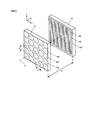
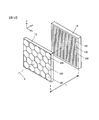
- FIG. 2 is a perspective view of the imaging unit 100.
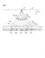
- FIG. FIG. 2 is a cross-sectional view schematically showing a photographic lens L1 and an imaging unit 100.
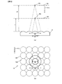
- 2 is a cross-sectional view schematically showing a light flux from a light spot on an image plane to be combined and an imaging unit 100.
- FIG. It is the schematic diagram which showed the breadth of the light about the light spot P4 and the light spot P5 on a respectively different image surface.
- FIG. It is a figure explaining the determination method of each incident area on an imaging surface in case the light beam from one light spot injects into many microlenses 120.
- FIG. It is a figure which shows the light spot P7 of the position which shifted
- PSF It is the top view which looked at the micro lens array 12 which concerns on 2nd Embodiment from the optical axis direction.
- the digital camera according to the present embodiment has a focal position desired by the user by numerical processing by using the fact that an image signal acquired by photographing through a microlens array has wavefront information such as depth information. Generate image data.
- the subject luminous flux incident through the photographing lens forms an image near the microlens array.
- the position at which the light beam forms an image according to the position of the subject differs in the optical axis direction of the photographing lens. Further, if the subject is a three-dimensional object, the subject light beam does not form an image on the same plane.
- the digital camera generates (synthesizes) image data that reproduces an image of a subject that is imaged at an imaging position in the optical axis direction desired by the user.
- the generated image data is referred to as composite image data.
- the composite image data appears as if the focal point of the imaging optical system is at the imaging position (not the actual imaging position but the position desired by the user). Therefore, in the following description, this imaging position is referred to as a focal position.
- the digital camera of the present embodiment is configured to be able to generate composite image data having a resolution larger than the number of microlenses included in the microlens array.
- the digital camera includes a large number of microlenses and a plurality of imaging pixels (light receiving elements) corresponding to the individual microlenses.
- the digital camera applies not only to the image signal output from the imaging pixel corresponding to one microlens but also to the microlens arranged in the periphery so as to be the composite image data of the focal position selected by the user.
- a composite image signal corresponding to an image formation region for one pixel of the composite image data is generated, and composite image data having a variable focal position is generated. Details will be described below.
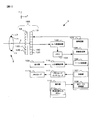
- FIG. 1 is a diagram showing a configuration of a digital camera according to the first embodiment.
- the digital camera 1 is configured such that the interchangeable lens 2 having the photographing lens L1 can be attached and detached by, for example, a bayonet type lens mount mechanism.
- the digital camera 1 includes an imaging unit 100, a control circuit 101, an A / D conversion circuit 102, a memory 103, an operation unit 112, a display 109, an LCD drive circuit 110, and a memory card interface 111.
- the imaging unit 100 includes a microlens array 12 and an imaging element 13 in which a large number of microlenses 120 are arranged two-dimensionally.
- the Z axis is set to be parallel to the optical axis of the photographic lens L1
- the X axis and the Y axis are set to be orthogonal to each other in a plane orthogonal to the Z axis.
- the photographing lens L1 is composed of a plurality of optical lens groups, and forms an image of a light beam from a subject near the focal plane.
- the photographing lens L1 is provided with a diaphragm 11 for adjusting the amount of incident light.
- the taking lens L1 is represented by a single lens for convenience of explanation.
- a microlens array 12 and an image sensor 13 are arranged in this order in the vicinity of the planned imaging plane of the photographic lens L1.
- the image sensor 13 is configured by a CCD or CMOS image sensor including a plurality of photoelectric conversion elements.
- the image sensor 13 captures a subject image formed on the imaging surface, and outputs a photoelectric conversion signal (image signal) corresponding to the subject image to the A / D conversion circuit 102 under the control of the control circuit 101.
- the details of the imaging unit 100 will be described later.
- the A / D conversion circuit 102 is a circuit that performs analog processing on the image signal output from the image sensor 13 and then converts it to a digital image signal.
- the control circuit 101 includes a CPU, a memory, and other peripheral circuits.
- the control circuit 101 reads and executes a control program stored in advance in a ROM (not shown) or the like. With this control program, the control circuit 101 performs a predetermined calculation using signals input from each unit constituting the digital camera 1 and sends a control signal to each unit of the digital camera 1 to control the photographing operation. Further, as will be described later, the control circuit 101 determines the focus position of the composite image data based on the operation signal input from the operation unit 112 in accordance with the operation of the focus position input button 112a.
- the control circuit 101 functionally includes an image composition unit 105, a Fourier transform unit 106, a division unit 107, and an inverse Fourier transform unit 108.
- the image composition unit 105 synthesizes composite image data of an arbitrary focal plane different from the planned focal plane of the photographic lens L1.
- the Fourier transform unit 106 performs Fourier transform on the synthesized image data synthesized by the image synthesis unit 105.
- the division unit 107 effectively divides the result of the Fourier transform by a Fourier image of a point spread function described later.
- the inverse Fourier transform unit 108 performs inverse Fourier transform on the result of division by the division unit 107 to create target image data. Details of the image composition unit 105, Fourier transform unit 106, division unit 107, and inverse Fourier transform unit 108 will be described later.
- the memory 103 is used to temporarily store the image signal digitally converted by the A / D conversion circuit 102, and data during or after the image processing, image compression processing, and display image data creation processing. It is a volatile storage medium.
- the memory card interface 111 is an interface that allows the memory card 111a to be attached and detached.
- the memory card interface 111 is an interface circuit that writes image data to the memory card 111a and reads image data recorded on the memory card 111a in accordance with the control of the control circuit 101.
- the memory card 111a is a semiconductor memory card such as a compact flash (registered trademark) or an SD card.
- the LCD drive circuit 110 is a circuit that drives the display 109 based on a command from the control circuit 101.
- the display device 109 is composed of a liquid crystal panel or the like, and displays display data created by the control circuit 101 based on image data recorded on the memory card 111a in the reproduction mode.
- the display 109 displays a menu screen for setting various operations of the digital camera 1.
- the operation unit 112 receives a user operation and outputs various operation signals corresponding to the operation content to the control circuit 101.
- the operation unit 112 includes a focus position input button 112a, a power button, a release button, other setting menu display switching buttons, a setting menu determination button, and the like.
- the focus position input button 112a is operated by the user when inputting the focus position y of the composite image data.
- the operation unit 112 outputs an operation signal including the focus position y to the control circuit 101.
- the imaging unit 100 includes a microlens array 12 and an imaging element 13.
- the microlens array 12 includes a plurality of microlenses 120 that are two-dimensionally arranged squarely on the XY plane.
- photoelectric conversion elements 130 (hereinafter referred to as imaging pixels 130) that receive light that has passed through each microlens 120 are two-dimensionally arranged in an arrangement pattern corresponding to the microlens 120.
- the image sensor 13 is arranged at a position away from the microlens array 12 by the focal length f of the microlens 120. That is, for each microlens 120, a plurality of imaging pixels 130 corresponding to (covered with) the microlens 120 are provided at positions separated by the focal length f of the microlens 120.
- FIG. 2 illustrates only a part of the plurality of microlenses 120 provided in the microlens array 12 and the plurality of imaging pixels 130 provided in the imaging element 13.
- about one hundred of the imaging pixels 130 are covered by one microlens 120, and thus the microlens array 12 has about a hundredth of the number of microlenses 120 of the number of imaging pixels 130 included in the imaging element 13. have.
- the focal length f of the microlens 120 is about several hundred micrometers (about one hundredth of the focal length of the photographing lens L1).
- the so-called exit pupil position of the photographic lens L1 can be regarded as almost infinite for the microlens 120. That is, the position of the exit pupil of the photographic lens L1 and the imaging surface of the imaging element 13 can be optically conjugate.
- FIG. 3 is a cross-sectional view schematically showing the photographing lens L1 and the imaging unit 100.
- a microlens array 12 is provided in the vicinity of the planned imaging plane S1 of the photographic lens L1 shown on the left side of FIG. 3, and an imaging element 13 is provided in the vicinity of the focal position S2 of the microlens 120.
- the subject image formed in the vicinity of the microlens array 12 by the photographing lens L1 is compressed by each microlens 120 included in the microlens array 12 and is folded into the image sensor 13.
- the image magnification of the photographic lens L1 is 1/50, that is, when the photographic lens L1 forms the subject image on the planned imaging plane S1 with an actual size of 1/50
- the subject image is viewed in the depth direction. Is imaged at a magnification of 1 / 2,500 which is its square. That is, the photographic lens L1 forms a three-dimensional image obtained by compressing the subject in the three-dimensional space in the depth direction on the planned imaging plane S1.
- FIG. 4 is a cross-sectional view schematically showing the light flux from the light spot on the image plane to be synthesized and the imaging unit 100.
- a light spot P1 provided on the image plane S3 to be synthesized is considered.
- the spread angle ⁇ 1 of light traveling from the light spot P1 toward the imaging unit 100 is limited by the size of the pupil of the photographing lens L1 (that is, the F value of the photographing lens L1). If the F value of the microlens 120 is equal to or smaller than the F value of the photographic lens L1, the light beam emitted from the light spot P1 and incident on a certain microlens 120 is in a region covered by the microlens 120. Does not spread outside.
- the light beams 30a to 30e incident on these microlenses 120a to 120e are incident on the imaging surface.
- the total radiation amount limited to the pupil from the light spot P1 can be obtained.
- the image composition unit 105 first identifies (1) a microlens 120 on which a light beam from the light point is incident with respect to a certain light spot on the image plane to be synthesized, and then (2) identifies For each microlens 120, it is specified to which imaging pixel the light beam from the light spot is incident.
- the angle of light spreading from the light spot can be specified by the pupil of the taking lens L1.
- the F value of the taking lens L1 is the same as the F value of the microlens 120.
- FIG. 5A is a cross-sectional view schematically showing the spread of the light spot P4 and the light spot P5 on different image planes, and FIG. 5B shows this from the photographic lens L1 side.
- FIG. The light beam from the light spot P4 existing on the image plane S4 at a position separated from the microlens 120 by the focal length f of the microlens 120 is spread to the size 31 of the microlens 120 for one microlens array. 12 is incident.
- the luminous flux from the light spot P5 existing on the image plane S5 at a position that is twice the focal length f of the microlens 120, that is, 2f away from the microlens 120, is shown in FIGS. 5 (a) and 5 (b). As shown in each of the figures, it spreads to a size 32 that exceeds one microlens 120.
- the microlens 120 on which the light beam from a certain light spot is incident is specified based on the distance from the light spot to the microlens 120 (that is, the distance from the image plane to be synthesized to the microlens 120). Can do. Actually, it is necessary to specify these microlenses 120 in consideration of the F value of the photographing lens L1. For example, when the F value of the photographing lens L1 is larger than the F value of the microlens 120 (the photographing lens L1 is darker than the microlens 120), the spread of the light beam from the light spot is small.
- the image composition unit 105 identifies (2) which imaging pixel the light flux from the light spot enters for each identified microlens 120. For example, when the light spot is at a position separated from the microlens 120 by the focal length f of the microlens 120 as in the light spot P4 of FIG. 5, a circular opening is formed in the entire region covered by the microlens 120 immediately below the microlens 120. The light spreads out. Therefore, in this case, all the imaging pixels 130 covered by one microlens 120 may be selected.
- the light spot when the light spot is located at a position closer than the focal length f from the microlens 120, the light spreads without converging at the microlens 120, but the spread is limited because the spread angle of the incident light beam is limited. It remains in the area covered with one microlens 120.
- the light spot when the light spot is at a position farther than the focal length f, the light flux from the light spot is incident on the plurality of microlenses 120, and therefore, from a large number of imaging pixels 130 covered by the plurality of microlenses 120. It is necessary to select an imaging pixel 130 necessary for creating a composite pixel.
- the case where the light spot is at a position farther than the focal distance f will be described by taking as an example the case where the light spot P5 in FIG. 5, that is, the light spot is at a position 2 f away from the microlens 120.
- the light flux from the light spot is a microlens 120 immediately below the light spot and eight microlenses 120 adjacent thereto. And a total of nine microlenses 120.
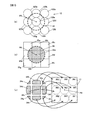
- FIG. 6 is a plan view of a part of the imaging surface of the imaging device 13 covered with the 25 microlenses 120 shown in FIG. 5B as seen from the optical axis direction.
- the position of each microlens 120 in FIG. 5B is indicated by a broken line superimposed on the imaging surface of the imaging element 13.
- the light beam from the light spot P5 shown in FIG. 5A is incident on the nine regions 33a to 33i shown in FIG. As is apparent from FIG. 6, these regions 33a to 33i have a shape in which the region covered by one microlens 120 is divided into nine.
- the size of the area on the imaging surface (the size of the light cross section) on which the light beam from the light spot is incident is covered by one microlens 120. It always matches the size of the area to be read.
- FIG. 7A is a plan view of a part of the microlens array 12 as viewed from the optical axis direction.
- the control circuit 101 specifies a range in which the light beam from the light spot P6 illustrated in the center of FIG.
- a region 34 extending over the nine microlenses 120a to 120i is a range where the light flux from the light spot P6 spreads.
- the region 34 is divided by a grid having the size of each microlens 120.
- squares 35a to 35i each having a diameter of each of the microlenses 120 arranged so as to correspond to each of the nine microlenses 120a to 120i shown in FIG.
- a region 34 where the light beam from the light spot P6 spreads is divided by the grating.
- the divided regions 34a to 34i are arranged in regions covered with the corresponding microlenses 120a to 120i, respectively.
- the relative positions of the divided areas 34a to 34i in each covering area are the same as the relative positions of the nine squares 35a to 35i shown in FIG. 7B.
- the divided area 34a corresponding to the square 35a in the upper left corner is arranged in the upper left corner of the corresponding covered area 36a.
- the region where the light flux from the light spot spreads is d / (h / f).
- (h / f) may be a negative value. In this case, it is assumed that there is a light spot on the image sensor 13 side from the microlens 120.
- the method of creating a composite pixel has been described by giving an example in which a light spot is on the lens central axis of a specific microlens 120.
- this method of creating a composite pixel can be used when a light spot exists at other positions. Can also be applied. If only the light spot on the lens central axis of the microlens 120 is synthesized, the number of pixels of the synthesized image data to be created is limited to the number of microlenses 120, and the synthesized image data having a low number of pixels. Can only be created. Therefore, the image composition unit 105 of the present embodiment sets a larger number of light spots on the image plane to be synthesized, and creates synthesized pixels for those light spots by the synthesis method described above, thereby increasing the number of pixels. Create composite image data.
- FIG. 8 is a diagram showing a light spot P7 at a position shifted by p to the left from the position of the light spot P5 with respect to the image plane S5 shown in FIG.
- the range 37 in which the light beam spreads is also shifted to the left by p. Therefore, by setting a divided region for the shifted range 37 in the same manner as in FIG. 7, a composite pixel corresponding to the light spot P7 can be created.
- a composite pixel corresponding to the light spot P7 can be created.
- the composite image data has 16 times the number of pixels as the number of microlenses 120.
- the output of one imaging pixel 130 is used to create a plurality of synthesis pixels.
- a large number of three-dimensional light spots are continuously present on the image plane to be synthesized, and light from these light spots is superimposed on the imaging plane of the image sensor 13. Therefore, when a light spot on the microlens 120 is provided, the light receiving output of the imaging pixel 130 into which the light beam from the light spot enters includes an output corresponding to the light beam from a light spot other than the light spot. Will be.
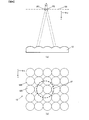
- FIG. 9 is a schematic diagram showing a state in which the light beams from the respective light spots overlap.
- FIG. 9A is a cross-sectional view of the image plane S4 to be synthesized, the microlens array 12, and the image pickup device 13 taken along the YZ plane.
- 9B is a plan view of the imaging surface of the imaging element 13 as viewed from the optical axis direction.
- five light spots P8 to P12 arranged in a line on the image plane S4 that is separated from the microlens 120 by the focal length f of the microlens 120.
- These five light spots P8 to P12 are provided at half the width d of the microlens 120, that is, at positions separated by d / 2. Specifically, the light spots P8, P10, and P12 are set at positions on the central axis of different microlenses 120, and the light spots P9 and P11 are set between two adjacent microlenses 120. At this time, the light beams 40 to 44 from the light spots P8 to P12 enter the regions 45 to 49 on the image pickup surface of the image pickup device 13 so as to overlap each other.
- the light beam 41 from the light spot P9 is incident on the region 46 shown in FIG. 9B.
- This region 46 is a region 45 where the light beam 40 from the light point P8 is incident and the light beam 42 from the light point P10. Overlaps with the incident region 47. That is, the light reception output from the imaging pixel 130 corresponding to the region where the region 45 and the region 46 overlap each other includes an output corresponding to the light beam 40 from the light point P8 and an output corresponding to the light beam 41 from the light point P9. It is superimposed.
- the output Pi of the composite pixel corresponding to the i-th light spot can be calculated by the following equation (1).
- the control circuit 101 divides one microlens 120 into four parts vertically and horizontally and provides 16 light spots.
- the output Pi of the combined pixel can be calculated using the following equation (2).
- the output distribution of the synthesized pixel at this time is shown in FIG.
- the vertical axis in FIG. 10 is the pixel output, and the horizontal axis is the pixel position.
- the synthesized pixel is a pixel output subjected to triangular convolution integration. From such an output distribution, a point spread function (PSF) representing how the light beam spreads from the light spot by the microlens 120 can be obtained.
- PSF point spread function
- PSF is determined from the arrangement of a plurality of microlenses 120 and the arrangement of pixels synthesized by the image synthesis unit 105.
- the size of the PSF is assumed to be equal to the size of the area covered by one microlens 120.
- the number of PSF elements is equal to the number of the plurality of imaging pixels 130 covered by one microlens 120.
- the output distribution of the synthesized pixel is illustrated one-dimensionally.
- the PSF can be obtained by performing calculation in consideration of not only the superimposition of the light beams from the left and right light spots but also the superposition of the light beams from all the surrounding light spots.
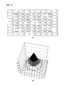
- FIG. 11A is a diagram showing the derived PSF value
- FIG. 11B is a diagram in which the PSF is plotted in three-dimensional coordinates.
- PSF values are shown for 81 points in one microlens 120.
- the division unit 107 solves the pixel output superposition shown in FIG. 10 using the PSF derived as described above.
- the superposition of pixel outputs can be expressed as the following equation (3). Here, for the sake of simplicity, it is expressed in one dimension.
- psf (t) represents PSF
- f (x) represents the true light intensity
- i (x) represents the superimposed pixel output. Since psf (t) is known by the above-described method and the superimposed pixel output i (x) is also known, the true light intensity f (x) can be obtained.
- i (x) is Fourier transformed
- the above equation (3) is expressed by the product of the Fourier transform image PSF (u) of PSF and the Fourier transform image F (u) of true light intensity f (x). It will be. That is, the Fourier transform image I (u) of i (x) is expressed as the following equation (4).
- the Fourier transform image F of the true light intensity f (x) from the above equation (5). (U) can be obtained. Thereafter, if the Fourier transform image F (u) is subjected to inverse Fourier transform, the true light intensity f (x) can be obtained.
- the division unit 107 of the present embodiment suppresses this high frequency noise using a known Wiener filter.
- the Wiener filter is applied to the above equation (5), the following equation (6) is obtained.
- the division unit 107 obtains a Fourier transform image F (u) of the true light intensity f (x) by the following equation (6) instead of the above equation (5), thereby obtaining clear composite image data in which high-frequency noise is suppressed. create.
- PSF * (u) means a complex conjugate of PSF (u).
- the imaging signal output from the imaging element 13 is converted into a digital image signal by the A / D conversion circuit 102 and stored in the memory 103.
- the control circuit 101 receives a focus position to be synthesized and an aperture value that determines the depth of field from the operation unit 112.
- the image synthesis unit 105 synthesizes a two-dimensional image of the input focal position and aperture value.
- the Fourier transform unit 106 determines a point spread function (PSF) for one light spot from the arrangement of the microlenses 120 in the microlens array 12 and the position of the synthesis pixel of the image synthesis unit 105, and this PSF and Fourier transform is performed on the composite image by the image composition unit 105.
- the dividing unit 107 effectively divides the Fourier image of the combined image by the image combining unit 105 by the Fourier image of the PSF using the Wiener filter as shown in the above equation (6), and the true light intensity f (x) is obtained.
- a Fourier image F (u) is obtained.
- the inverse Fourier transform unit 108 performs inverse Fourier transform on the Fourier image F (u) to obtain improved target image data from the original synthesized image data.
- This image is a high-contrast image in which the superposition of the incident light beam by the microlens 120 is solved.
- the digital camera 1 corresponds to each of the microlens array 12 including a plurality of microlenses 120 arranged two-dimensionally so that a light beam transmitted through the photographing lens L1 is incident thereon, and each of the plurality of microlenses 120. And an imaging device 13 having a plurality of imaging pixels 130 arranged on the rear side of the microlens 120.
- the control circuit 101 based on the output of the plurality of imaging pixels 130 corresponding to each of the plurality of microlenses 120, an image composition unit 105 that composes image data of an image on an arbitrary image plane of the photographing lens L 1, and image composition
- the Fourier transform unit 106 that performs Fourier transform on the image data synthesized by the unit 105, and the Fourier transform result is effectively divided by the Fourier image of the point spread function that represents the optical spread of the light beam incident on the plurality of microlenses 120.
- a division unit 107 that performs the inverse Fourier transform on the result of the division by the division unit 107 and generates target image data. Since this is done, it is possible to synthesize image data having both high contrast and high resolution.
- the division unit 107 effectively divides the result of the Fourier transform by the Fourier transform unit 106 by applying a Wiener filter based on the Fourier image of the point spread function to the result of the Fourier transform by the Fourier transform unit 106. Since it did in this way, the clear image in which the high frequency noise was suppressed can be obtained.
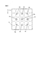
- FIG. 12 is a plan view of the microlens array 12 according to the second embodiment viewed from the optical axis direction. As shown in FIG. 12, in this embodiment, hexagonal microlenses 120 constituting a honeycomb structure are used. The present invention can also be applied to the microlens 120 having such a shape as in the first embodiment.
- the PSF used in this embodiment is different from that of the first embodiment.
- the derivation method itself is the same as that of the first embodiment. That is, the superimposition of the light beams from the surrounding light spots as shown in FIG. 10 may be calculated two-dimensionally.
- Modification 1 Although an embodiment in which the present invention is applied to a digital camera with interchangeable lenses has been described above, the present invention is not limited to such an embodiment.
- the present invention can be applied to a lens-integrated camera or the like.
- the arrangement and shape of the microlenses 120 are not limited to those described in the first and second embodiments. The same applies to the arrangement and shape of each imaging pixel on the imaging surface of the imaging element 13.
- the imaging pixel 130 covered with each microlens 120 may be separated for each microlens 120.
- the true light intensity f (x) may be obtained without using the Wiener filter. That is, the dividing unit 107 may be configured to obtain F (u) using (4) instead of the above equation (5).
- the high-pass filter is effective for the original image before composition, not for the composite image.
- the image is an image near the focal position of the microlens, and the intensity change with respect to the one-dimensional position is defined as f (x).
- the diameter of the microlens is S
- the light output spreads from this position by S, and therefore the intensity at the image sensor is f (x) / S. Because the position x 0 on a certain image sensor surface is a superposition of such light It can be expressed.
- FIG. 13 is a conceptual diagram for explaining the contents that complement the contrast that is lowered by adding a high-pass filter. If the spatial frequency is lower than the microlens density, there is no particular problem in the contrast of the composite image. However, if the spatial frequency is higher than the microlens density, the contrast of the composite image is lowered due to the influence of superposition. Therefore, high-pass filter processing is performed on the original image before synthesis to emphasize a portion having a high spatial frequency in advance. Thereby, even if the image composition of an arbitrary image plane as in the present application is performed, the reduction in contrast of the portion having a high spatial frequency is complemented.
- FIG. 14 is a diagram showing a configuration of a control circuit 101A for carrying out this modification.
- the control circuit 101A includes a high-pass filter unit 201 and an image composition unit 105.
- the Fourier transform unit 106, the division unit 107, and the inverse Fourier transform unit 108 of the control circuit 101 in FIG. 1 are deleted, and a high-pass filter unit 201 is provided instead. Since the image composition unit 105 is the same as the image composition unit 105 of the above embodiment, the same reference numerals are given.
- the original image data before image synthesis is input from the memory 103 to the control circuit 101A, it is first input to the high-pass filter unit 201 and subjected to high-pass filter processing. Thereafter, a two-dimensional image of the focus position and aperture value input to the image composition unit 105 and instructed by the operation unit 112 is synthesized as in the above embodiment. Thereafter, the synthesized image after synthesis is output.
- the present invention is not limited to the above-described embodiments, and other forms conceivable within the scope of the technical idea of the present invention are also included in the scope of the present invention. .
- SYMBOLS 1 Digital camera, 2 ... Interchangeable lens, 12 ... Micro lens array, 13 ... Imaging element, 101 ... Control circuit, 105 ... Image composition part, 106 ... Fourier transformation part, 107 ... Division part, 108 ... Inverse Fourier transformation part, 120 ... microlens, 130 ... imaging pixel, L1 ... photographing lens
Landscapes
- Engineering & Computer Science (AREA)
- Multimedia (AREA)
- Signal Processing (AREA)
- Studio Devices (AREA)
- Image Processing (AREA)
- Image Input (AREA)
Abstract
Description
本発明の第2の態様によると、第1の態様の撮像装置において、画素に対応する複数の受光素子からの信号と、他の画素に対応する複数の受光素子からの信号には重複している受光素子からの信号が含まれ、画像処理部は、画素に対応する複数の受光素子からの信号から重複している他の画素の信号を除去することが好ましい。
本発明の第3の態様によると、撮像装置は、撮影光学系を透過した光束が入射するよう二次元状に配置された複数のマイクロレンズと、複数のマイクロレンズの各々に対応して当該マイクロレンズの後側に配置された複数の受光素子と、複数のマイクロレンズの各々に対応する複数の受光素子の出力に基づいて、撮影光学系の任意の像面における像の画像データを合成する画像合成部と、画像合成部により合成された画像データをフーリエ変換するフーリエ変換部と、複数のマイクロレンズに入射した光束の光学的な広がりを表すポイントスプレッドファンクションのフーリエ像でフーリエ変換部によるフーリエ変換の結果を実効的に除算する演算部と、演算部による除算の結果を逆フーリエ変換し、目的画像データを作成する逆フーリエ変換部とを備える。
本発明の第4の態様によると、第3の態様の撮像装置において、演算部は、ポイントスプレッドファンクションのフーリエ像に基づくウィナーフィルタをフーリエ変換部によるフーリエ変換の結果に適用することにより、フーリエ変換部によるフーリエ変換の結果を実効的に除算することが好ましい。
本発明の第4の態様によると、第3または4の態様の撮像装置において、ポイントスプレッドファンクションの大きさは1つのマイクロレンズが被覆する領域の大きさと等しいことが好ましい。
本発明の第6の態様によると、第5の態様の撮像装置において、ポイントスプレッドファンクションの要素数は1つのマイクロレンズが被覆する複数の受光素子の数に等しいことが好ましい。
本発明の第7の態様によると、第3~6のいずれか一態様の撮像装置において、ポイントスプレッドファンクションは、複数のマイクロレンズの配列と、画像合成部が合成する画素の配列とから決定されることが好ましい。
本実施の形態のデジタルカメラは、マイクロレンズアレイを介して撮影することにより取得された画像信号が奥行き情報等の波面情報を有することを利用して、数値処理によってユーザが所望する焦点位置を有する画像データを生成する。撮影レンズを介して入射した被写体光束は、マイクロレンズアレイの近傍に結像する。このとき、被写体の位置に応じて光束が結像する位置は撮影レンズの光軸方向に異なるものとなり、さらに被写体が三次元物体であれば被写体光束は同一平面上には結像しない。本実施の形態のデジタルカメラは、ユーザが所望する光軸方向の結像位置に結像する被写体の像を再現した画像データを生成(合成)する。以下、この生成された画像データを合成画像データと称する。合成画像データは、結像光学系の焦点があたかも当該結像位置(実際の結像位置ではなくユーザが所望する位置)にあるように見える。そこで、以下の説明において、この結像位置のことを焦点位置と呼ぶこととする。




(1)デジタルカメラ1は、撮影レンズL1を透過した光束が入射するよう二次元状に配置された複数のマイクロレンズ120から成るマイクロレンズアレイ12と、複数のマイクロレンズ120の各々に対応して当該マイクロレンズ120の後側に配置された複数の撮像画素130を有する撮像素子13とを備える。制御回路101は、複数のマイクロレンズ120の各々に対応する複数の撮像画素130の出力に基づいて、撮影レンズL1の任意の像面における像の画像データを合成する画像合成部105と、画像合成部105により合成された画像データをフーリエ変換するフーリエ変換部106と、複数のマイクロレンズ120に入射した光束の光学的な広がりを表すポイントスプレッドファンクションのフーリエ像でフーリエ変換の結果を実効的に除算する除算部107と、除算部107による除算の結果を逆フーリエ変換し、目的画像データを作成する逆フーリエ変換部108と、を備える。このようにしたので、コントラストの高さと分解能の高さを両立した画像データを合成することができる。
以下、図面を用いて、本発明の第2の実施の形態であるデジタルカメラについて説明する。なお、第1の実施の形態と同一の箇所には第1の実施の形態と同一の符号を付し、説明を省略する。
レンズ交換可能なデジタルカメラに本発明を適用した実施形態について上述したが、本発明はこのような実施の形態に限定されない。例えばレンズ一体型のカメラ等についても本発明を適用することが可能である。
マイクロレンズ120の配列および形状は、第1および第2の実施の形態で述べたものに限定されない。また、撮像素子13の撮像面における各撮像画素の配列および形状についても同様である。例えば、各マイクロレンズ120により被覆される撮像画素130が、マイクロレンズ120毎に分離していてもよい。
ウィナーフィルタを用いずに真の光強度f(x)を求めてもよい。すなわち、上式(5)ではなく(4)を用いてF(u)を求めるように除算部107を構成してもよい。
上記実施の形態では、画像合成部105により合成された合成画像に対して、フーリエ変換部106、除算部107、逆フーリエ変換部108の処理により、マイクロレンズ120による入射光束の重畳を解き、コントラストの高い画像を求めるようにした。しかし、合成前の画像の空間周波数成分が高い部分にハイパスフィルターを加え、低下するコントラストをあらかじめ補完しておくようにしてもよい。

とあらわすことができる。

と考えることができる。
日本国特許出願2012年第156940号(2012年7月12日出願)
Claims (7)
- 二次元状に配置された複数のマイクロレンズと、
前記複数のマイクロレンズに対応して配置された複数の受光素子と、
前記複数の受光素子からの信号に基づいて、撮影光学系の任意の像面における画像を合成する画像合成部と、
前記画像合成部で合成された画像を構成する画素の信号から他の画素の信号を除去する画像処理部とを備える撮像装置。 - 請求項1に記載の撮像装置において、
前記画素に対応する複数の受光素子からの信号と、前記他の画素に対応する複数の受光素子からの信号には重複している受光素子からの信号が含まれ、
前記画像処理部は、前記画素に対応する複数の受光素子からの信号から前記重複している他の画素の信号を除去する撮像装置。 - 撮影光学系を透過した光束が入射するよう二次元状に配置された複数のマイクロレンズと、
前記複数のマイクロレンズの各々に対応して当該マイクロレンズの後側に配置された複数の受光素子と、
前記複数のマイクロレンズの各々に対応する前記複数の受光素子の出力に基づいて、前記撮影光学系の任意の像面における像の画像データを合成する画像合成部と、
前記画像合成部により合成された前記画像データをフーリエ変換するフーリエ変換部と、
前記複数のマイクロレンズに入射した光束の光学的な広がりを表すポイントスプレッドファンクションのフーリエ像で前記フーリエ変換部によるフーリエ変換の結果を実効的に除算する演算部と、
前記演算部による前記除算の結果を逆フーリエ変換し、目的画像データを作成する逆フーリエ変換部とを備える撮像装置。 - 請求項3に記載の撮像装置において、
前記演算部は、前記ポイントスプレッドファンクションのフーリエ像に基づくウィナーフィルタを前記フーリエ変換部によるフーリエ変換の結果に適用することにより、前記フーリエ変換部によるフーリエ変換の結果を実効的に除算する撮像装置。 - 請求項3または4に記載の撮像装置において、
前記ポイントスプレッドファンクションの大きさは1つの前記マイクロレンズが被覆する領域の大きさと等しい撮像装置。 - 請求項5に記載の撮像装置において、
前記ポイントスプレッドファンクションの要素数は1つの前記マイクロレンズが被覆する前記複数の受光素子の数に等しい撮像装置。 - 請求項3~6のいずれか一項に記載の撮像装置において、
前記ポイントスプレッドファンクションは、前記複数のマイクロレンズの配列と、前記画像合成部が合成する画素の配列とから決定される撮像装置。
Priority Applications (4)
| Application Number | Priority Date | Filing Date | Title |
|---|---|---|---|
| CN201380036923.6A CN104471924B (zh) | 2012-07-12 | 2013-07-12 | 拍摄装置 |
| US14/413,288 US9838618B2 (en) | 2012-07-12 | 2013-07-12 | Image processing device configured to correct output data based upon a point spread function |
| JP2014524899A JP6344236B2 (ja) | 2012-07-12 | 2013-07-12 | 画像処理装置および撮像装置 |
| US15/807,103 US10341580B2 (en) | 2012-07-12 | 2017-11-08 | Image processing device configured to correct an image so as to decrease output data |
Applications Claiming Priority (2)
| Application Number | Priority Date | Filing Date | Title |
|---|---|---|---|
| JP2012-156940 | 2012-07-12 | ||
| JP2012156940 | 2012-07-12 |
Related Child Applications (2)
| Application Number | Title | Priority Date | Filing Date |
|---|---|---|---|
| US14/413,288 A-371-Of-International US9838618B2 (en) | 2012-07-12 | 2013-07-12 | Image processing device configured to correct output data based upon a point spread function |
| US15/807,103 Continuation US10341580B2 (en) | 2012-07-12 | 2017-11-08 | Image processing device configured to correct an image so as to decrease output data |
Publications (1)
| Publication Number | Publication Date |
|---|---|
| WO2014010734A1 true WO2014010734A1 (ja) | 2014-01-16 |
Family
ID=49916173
Family Applications (1)
| Application Number | Title | Priority Date | Filing Date |
|---|---|---|---|
| PCT/JP2013/069193 Ceased WO2014010734A1 (ja) | 2012-07-12 | 2013-07-12 | 撮像装置 |
Country Status (4)
| Country | Link |
|---|---|
| US (2) | US9838618B2 (ja) |
| JP (2) | JP6344236B2 (ja) |
| CN (2) | CN108337419A (ja) |
| WO (1) | WO2014010734A1 (ja) |
Families Citing this family (3)
| Publication number | Priority date | Publication date | Assignee | Title |
|---|---|---|---|---|
| JP5671842B2 (ja) * | 2010-06-03 | 2015-02-18 | 株式会社ニコン | 画像処理装置および撮像装置 |
| CN105812623B (zh) * | 2014-12-30 | 2018-10-16 | 深圳超多维科技有限公司 | 微透镜阵列成像装置与成像方法 |
| KR102554417B1 (ko) * | 2018-06-18 | 2023-07-11 | 삼성전자주식회사 | 이미지 센서 |
Citations (2)
| Publication number | Priority date | Publication date | Assignee | Title |
|---|---|---|---|---|
| JP2010258689A (ja) * | 2009-04-23 | 2010-11-11 | Canon Inc | 画像復元装置 |
| WO2012043211A1 (ja) * | 2010-10-01 | 2012-04-05 | 富士フイルム株式会社 | 撮像装置 |
Family Cites Families (19)
| Publication number | Priority date | Publication date | Assignee | Title |
|---|---|---|---|---|
| CN1219395C (zh) * | 2002-01-30 | 2005-09-14 | 株式会社理光 | 摄像装置和摄像方法 |
| US7173663B2 (en) * | 2002-10-31 | 2007-02-06 | Freescale Semiconductor, Inc. | Automatic exposure control system for a digital camera |
| US20050133879A1 (en) * | 2003-04-07 | 2005-06-23 | Takumi Yamaguti | Solid-state imaging device, signal processing device, camera, and spectral device |
| US20070279618A1 (en) * | 2004-10-15 | 2007-12-06 | Matsushita Electric Industrial Co., Ltd. | Imaging Apparatus And Image Improving Method |
| CA2609623C (en) * | 2005-06-03 | 2015-12-29 | Universitaet Zuerich | Photoarray for detecting time-dependent image data |
| JP4826152B2 (ja) * | 2005-06-23 | 2011-11-30 | 株式会社ニコン | 画像合成方法及び撮像装置 |
| JP4444936B2 (ja) * | 2006-09-19 | 2010-03-31 | 富士フイルム株式会社 | 撮影装置および方法並びにプログラム |
| US7792423B2 (en) * | 2007-02-06 | 2010-09-07 | Mitsubishi Electric Research Laboratories, Inc. | 4D light field cameras |
| US8229294B2 (en) * | 2007-12-10 | 2012-07-24 | Mitsubishi Electric Research Laboratories, Inc. | Cameras with varying spatio-angular-temporal resolutions |
| JP5187145B2 (ja) * | 2008-11-07 | 2013-04-24 | 株式会社ニコン | 画像合成装置および方法 |
| JP5463718B2 (ja) * | 2009-04-16 | 2014-04-09 | ソニー株式会社 | 撮像装置 |
| JP5499778B2 (ja) * | 2010-03-03 | 2014-05-21 | 株式会社ニコン | 撮像装置 |
| JP5671842B2 (ja) * | 2010-06-03 | 2015-02-18 | 株式会社ニコン | 画像処理装置および撮像装置 |
| CN103155542A (zh) * | 2010-09-24 | 2013-06-12 | 富士胶片株式会社 | 图像拾取装置和图像拾取设备 |
| US20140176592A1 (en) * | 2011-02-15 | 2014-06-26 | Lytro, Inc. | Configuring two-dimensional image processing based on light-field parameters |
| JP2012222742A (ja) * | 2011-04-13 | 2012-11-12 | Sony Corp | 撮像素子および撮像装置 |
| WO2012147245A1 (ja) * | 2011-04-27 | 2012-11-01 | パナソニック株式会社 | 撮像装置、撮像装置を備える撮像システム、及び撮像方法 |
| CN105866917A (zh) * | 2011-05-31 | 2016-08-17 | 株式会社尼康 | 镜头镜筒及相机机身 |
| WO2014178607A1 (ko) * | 2013-05-02 | 2014-11-06 | 주식회사 레이언스 | 이미지센서와 이의 구동방법 |
-
2013
- 2013-07-12 JP JP2014524899A patent/JP6344236B2/ja active Active
- 2013-07-12 US US14/413,288 patent/US9838618B2/en active Active
- 2013-07-12 WO PCT/JP2013/069193 patent/WO2014010734A1/ja not_active Ceased
- 2013-07-12 CN CN201810281528.9A patent/CN108337419A/zh active Pending
- 2013-07-12 CN CN201380036923.6A patent/CN104471924B/zh active Active
-
2017
- 2017-11-08 US US15/807,103 patent/US10341580B2/en active Active
-
2018
- 2018-05-24 JP JP2018099866A patent/JP6516045B2/ja active Active
Patent Citations (2)
| Publication number | Priority date | Publication date | Assignee | Title |
|---|---|---|---|---|
| JP2010258689A (ja) * | 2009-04-23 | 2010-11-11 | Canon Inc | 画像復元装置 |
| WO2012043211A1 (ja) * | 2010-10-01 | 2012-04-05 | 富士フイルム株式会社 | 撮像装置 |
Also Published As
| Publication number | Publication date |
|---|---|
| US20180070027A1 (en) | 2018-03-08 |
| US20150319351A1 (en) | 2015-11-05 |
| CN108337419A (zh) | 2018-07-27 |
| JP6344236B2 (ja) | 2018-06-20 |
| JP2018186508A (ja) | 2018-11-22 |
| US9838618B2 (en) | 2017-12-05 |
| US10341580B2 (en) | 2019-07-02 |
| JPWO2014010734A1 (ja) | 2016-06-23 |
| CN104471924A (zh) | 2015-03-25 |
| JP6516045B2 (ja) | 2019-05-22 |
| CN104471924B (zh) | 2018-05-01 |
Similar Documents
| Publication | Publication Date | Title |
|---|---|---|
| JP6149339B2 (ja) | 表示装置 | |
| WO2011152531A1 (ja) | 撮像装置 | |
| JP4941332B2 (ja) | 撮像装置 | |
| JP4967873B2 (ja) | 撮像装置 | |
| JP2010114758A (ja) | 画像合成装置および方法 | |
| JP6397281B2 (ja) | 撮像装置、その制御方法およびプログラム | |
| JP6516045B2 (ja) | 画像処理装置 | |
| JP7642022B2 (ja) | 計測装置、撮像装置、制御方法及びプログラム | |
| JP6036799B2 (ja) | 画像処理装置 | |
| JP6376206B2 (ja) | 画像処理装置および撮像装置 | |
| JP6102061B2 (ja) | 画像処理装置 | |
| WO2021171980A1 (ja) | 画像処理装置及びその制御方法並びにプログラム | |
| WO2017126242A1 (ja) | 撮像装置、及び、画像データ生成方法 | |
| JP2014155071A (ja) | 画像処理装置、撮像装置、制御方法、及びプログラム | |
| JP2016082325A (ja) | 撮像装置、画像処理装置および画像処理プログラム | |
| JP2016031446A (ja) | 撮像装置及びその制御方法 | |
| KR20130106525A (ko) | 영상 처리 장치 및 이의 영상 처리 방법 | |
| JP6593428B2 (ja) | 表示装置 | |
| JP2018098738A (ja) | 画像処理装置、撮像装置、画像処理方法および画像処理プログラム | |
| JP6491539B2 (ja) | 撮像装置及びその制御方法、システムならびにプログラム | |
| JP2015220599A (ja) | 情報処理装置、制御方法、プログラム及び記録媒体 | |
| JP6387149B2 (ja) | 画像処理装置、撮像装置、制御方法、及びプログラム |
Legal Events
| Date | Code | Title | Description |
|---|---|---|---|
| 121 | Ep: the epo has been informed by wipo that ep was designated in this application |
Ref document number: 13816028 Country of ref document: EP Kind code of ref document: A1 |
|
| ENP | Entry into the national phase |
Ref document number: 2014524899 Country of ref document: JP Kind code of ref document: A |
|
| NENP | Non-entry into the national phase |
Ref country code: DE |
|
| WWE | Wipo information: entry into national phase |
Ref document number: 14413288 Country of ref document: US |
|
| 122 | Ep: pct application non-entry in european phase |
Ref document number: 13816028 Country of ref document: EP Kind code of ref document: A1 |