WO2014010309A1 - 検査方法、検査装置及びガラス板の製造方法 - Google Patents
検査方法、検査装置及びガラス板の製造方法 Download PDFInfo
- Publication number
- WO2014010309A1 WO2014010309A1 PCT/JP2013/064013 JP2013064013W WO2014010309A1 WO 2014010309 A1 WO2014010309 A1 WO 2014010309A1 JP 2013064013 W JP2013064013 W JP 2013064013W WO 2014010309 A1 WO2014010309 A1 WO 2014010309A1
- Authority
- WO
- WIPO (PCT)
- Prior art keywords
- inspection
- glass plate
- angle
- measured
- point
- Prior art date
- Legal status (The legal status is an assumption and is not a legal conclusion. Google has not performed a legal analysis and makes no representation as to the accuracy of the status listed.)
- Ceased
Links
Images




Classifications
-
- G—PHYSICS
- G01—MEASURING; TESTING
- G01N—INVESTIGATING OR ANALYSING MATERIALS BY DETERMINING THEIR CHEMICAL OR PHYSICAL PROPERTIES
- G01N21/00—Investigating or analysing materials by the use of optical means, i.e. using sub-millimetre waves, infrared, visible or ultraviolet light
- G01N21/84—Systems specially adapted for particular applications
- G01N21/88—Investigating the presence of flaws or contamination
- G01N21/95—Investigating the presence of flaws or contamination characterised by the material or shape of the object to be examined
- G01N21/958—Inspecting transparent materials or objects, e.g. windscreens
Definitions
- the present invention relates to a method for inspecting a glass plate, and more particularly to a method for inspecting a colored layer formed on the glass plate.
- the glass plate attached to the window of an automobile may be provided with a black coating layer on the periphery.
- the black coating layer is a black and belt-like layer formed by screen-printing a ceramic paste made of a low melting point glass powder and a pigment in the form of a paste on a glass surface and then baking it.
- Japanese Patent Application Laid-Open No. 2004-243630 describes that a black coating layer is formed on a glass plate by screen printing.
- Japanese Patent Laid-Open No. 2006-105807 illuminates a printed material using scattered light, images a plurality of images of the printed material with a CCD camera from the side through which the scattered light is transmitted, and combines the images to inspect an image.
- the inspection image is binarized into a dark part and a bright part, the bright parts are ordered in descending order of the area, and the size of the area becomes (m + 1) th or less (m is the number of non-printing parts).
- An inspection method is described in which bright portions are defined as printing defects, dark portions are ordered in descending order of area, and dark portions having an area size equal to or smaller than (n + 1) th (n is the number of printed portions) are printed stains.
- Japanese Patent Laid-Open No. 2004-188646 prepares in advance threshold standard data created by associating a standard value of an inspection threshold value with the type of element solder printing portion, A print inspection method is described in which a threshold value is set for each element solder printing portion of a board based on the threshold standard data according to the type of the element solder printing portion.
- Japanese Patent Application Laid-Open No. 2004-58298 discloses an inspection object created by classifying unit shape / position data indicating the shape and position of a unit printing portion printed on an electrode according to a grouping condition into a data group.
- a print inspection method for determining a printing state by comparing data and an imaging result of a substrate by an imaging unit is described.
- Japanese Patent Application Laid-Open No. 2004-58298 is for recognizing small cream solder, and is applied to a black coating layer printed on the periphery of a large glass plate having a vertical and horizontal size exceeding 1 m. It is not possible to determine the small chip that has occurred.
- the object of the present invention is to accurately detect chipping in the black coating layer.
- a representative embodiment of the present invention is a method for inspecting defects in a colored layer formed on a glass plate, and a plurality of images are formed on the boundary of the colored layer using an image of the glass plate to be inspected.
- a first step of setting the inspection point a second step of measuring an angle formed by two line segments connecting the set inspection point and the adjacent inspection points on both sides, and the measurement
- FIG. 1A is a plan view of a glass plate 1 to be inspected by the inspection apparatus according to the embodiment of the present invention
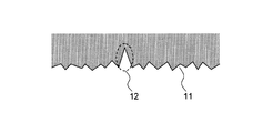
- FIG. 1B is an enlarged view of a portion A of the glass plate 1.
- the illustrated glass plate 1 is a glass plate attached to a window of an automobile, and a black coating layer is provided on the peripheral edge thereof.
- the black coating layer is a usually black and belt-like layer formed by screen-printing a ceramic paste made of a low melting point glass powder and a pigment in the form of a paste on a glass surface and then baking it.
- the inspection apparatus discriminates the black coating layer from bleeding and chipping, and accurately detects the chipping.
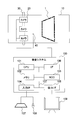
- FIG. 2 is a block diagram showing the configuration of the inspection apparatus according to the embodiment of the present invention.
- the inspection apparatus includes a conveyor 10 that conveys a glass plate 1 to be inspected, a camera 20 that photographs the glass plate 1 being conveyed, a lamp 30 that irradiates light on the glass plate 1 photographed by the camera 20, and a conveyor.
- 10 includes a sensor 40 for detecting the glass plate 1 on the top 10 and an inspection system 100 for analyzing an image taken by the camera 20.
- the camera 20 is an imaging device that captures a conveyed glass plate 1 and obtains a black and white image of the glass plate.
- a CCD line sensor can be used.
- a line sensor is used for the camera 20
- a plane image of the glass plate to be inspected can be obtained by continuously acquiring images (for example, moving images) according to the conveyance of the glass plate 1.
- a CCD camera or a CMOS sensor in which image sensors are arranged two-dimensionally (planar) may be used instead of a line sensor in which image sensors are arranged one-dimensionally.
- the inspection apparatus includes a plurality of cameras 20 in order to improve the resolution of a captured image.
- An image captured by the camera 20 is input to the inspection system 100.
- the lamp 30 is a light emitting element that irradiates light on the glass plate 1 photographed by the camera 20 from the back side of the conveyor 10 (opposite side of the camera 20).
- a fluorescent lamp can be used.
- the lamp 30 may be a high-frequency fluorescent lamp that operates at a cycle earlier than the shooting interval of the camera 20.
- the sensor 40 is a sensor that detects that the glass plate 1 transported on the conveyor 10 has been placed on the sensor 40 (that is, has reached a position suitable for photographing by the camera 20). For example, a photoelectric switch is used. Can do.
- a signal output from the sensor 40 is input to the inspection system 100.
- the inspection system 100 captures an image acquired by the camera 20 based on a signal output from the sensor 40.
- the inspection system 100 includes a processor (CPU) 101, a memory 102, a storage device (HDD) 103, an input device 104, an output device 105, and an interface 106, and these components are connected via a bus 107. It is.
- the processor 101 is a processing device that executes a program stored in the memory 102.
- the memory 102 is a high-speed and volatile storage device such as a DRAM (Dynamic Random Access Memory), and stores an operating system (OS) and application programs.
- OS operating system
- the processor 101 executes the operating system, the basic function of the computer is realized, and when the application program is executed, the function provided by the computer is realized.
- the memory 102 stores a program for executing the reference value acquisition process shown in FIG. 5 and the missing detection process shown in FIG.
- the storage device 103 is a large-capacity nonvolatile storage device such as a magnetic storage device or a flash memory, and stores a program executed by the processor 101 and data used when the program is executed.
- the program is read from the storage device 103, loaded into the memory 102, and executed by the processor 101.
- the input device 104 is connected to user interfaces such as a keyboard 107 and a mouse 108.
- a user interface such as a display device 109 and a printer is connected to the output device 105.
- the input device 104 and the output device 105 may be configured with an interface capable of inputting and outputting data, such as a USB and an optical disk drive.
- the interface 106 connects the inspection system 100 to the camera 20 and the sensor 40.
- the interface 106 may include a communication interface that controls communication with other devices.
- the inspection system 100 may be physically constructed on one computer, or may be constructed on a logical partition physically configured on one or a plurality of computers.
- the program executed by the processor 101 is provided to the computer via a nonvolatile storage medium or a network.
- the computer may be provided with an interface for reading a storage medium (CD-ROM, flash memory, etc.).
- FIG. 5 is a flowchart of the reference value acquisition process according to the embodiment of the present invention. This reference value acquisition process is executed by the processor 101 of the inspection system 100.
- the glass plate to be manufactured is visually inspected to obtain image data (reference value) of the glass plate that can be determined to be good (S101).
- image data reference value
- tip of a black coating layer is found in the glass plate for reference value acquisition, a reference value is acquired using another glass plate.
- enlargement / reduction processing is performed to smooth the boundary line of the black coating layer (S102).
- the enlargement / reduction process may be performed a plurality of times. This is because if the number of enlargement / reduction processes is small, the unevenness of the boundary of the black coating layer due to bleeding becomes rough, and the possibility of erroneous detection in the chipping detection process increases. Moreover, you may perform the smoothing process which smooths a line which is not an expansion / contraction process. By performing the smoothing process, it is possible to smooth the unevenness of the boundary due to bleeding of the black coating layer, to obtain an accurate reference value, and to reduce false detection of a chip.
- the acquired image data may be binarized to clarify the boundary of the black coating layer.
- the subsequent processes can be speeded up.
- it may be determined that a portion where the luminance change in the image is large is a boundary. In this way, the boundary can be accurately defined even when the boundary line of the black coating layer is thin.
- a plurality of inspection points are set on the boundary of the black coating layer, and formed by line segments connecting the coordinates of the inspection points and the inspection points adjacent to the inspection points.
- the angle (angle ⁇ formed by line segment BC and line segment CD in FIG. 3) is measured (S103).
- a predetermined algorithm such as a Douglas-Poiker algorithm or a cone intersection method can be used for setting the inspection point.
- the preset detection angle is compared with the measured angle of the inspection point (S104).
- the angle of the inspection point is smaller than the detection angle, it is determined that the measured inspection point angle is the shape of the boundary of the normal black coating layer, and the coordinates of the inspection point and the measured angle are the reference values. Is stored in the memory 102 (S105). On the other hand, if the angle of the inspection point is equal to or larger than the detection angle, it is determined that the measured inspection point angle is an abnormal value, and the process returns to step S103 to measure the angle of the next inspection point.
- step S106 it is determined whether the measurement of the angles of all the inspection points has been completed. If the measurement of the angles of all the inspection points has been completed, the reference value acquisition process is terminated. On the other hand, if there is an inspection point for which the angle measurement has not been completed, the process returns to step S103, and the angle of the next inspection point is measured.
- tip detection process of embodiment of this invention is demonstrated.
- the manufactured glass plate is cut into a desired shape.
- the black coating layer is inspected (see FIG. 6).
- a silver paste is printed and baked to form a defogger hot wire or an antenna.
- the glass plate is bent to a predetermined curvature.
- Pre-adhesion for deaeration between glass plates is performed.
- Heat and press in an autoclave and finish bonding is performed by pressing the intermediate film.
- the intermediate film protruding from the glass plate is cut.
- the manufacturing process described above is merely an example of a normal process except for the inspection process (4), and may be different from the process described in the specification except for the inspection process (4).
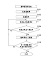
- FIG. 6 is a flowchart of the chip detection process according to the embodiment of the present invention.
- a reference value of a glass plate having the same model number as the glass plate 1 to be inspected is acquired, and the reference value is confirmed (S201).
- enlargement / reduction processing is performed to smooth the boundary line of the black coating layer (S202).
- the enlargement / reduction process may be performed a plurality of times. This is because if the number of times of enlargement / reduction processing is small, the unevenness at the boundary of the black coating layer becomes rough due to bleeding, and the possibility of erroneous detection increases. Moreover, you may perform the smoothing process which smooths a line which is not an expansion / contraction process. By performing the smoothing process, the unevenness of the boundary due to the blurring of the black coating layer can be smoothed, and the erroneous detection of the chip can be reduced.
- the acquired image data may be binarized to clarify the boundary of the black coating layer.
- the subsequent processes can be speeded up.
- it may be determined that a portion where the luminance change in the image is large is a boundary. In this way, the boundary can be accurately defined even when the boundary line of the black coating layer is thin.
- the first inspection point is defined on the boundary line of the black coating layer (S203), a plurality of inspection points (points A to E in FIG. 4) are set, and the coordinates of each inspection point and the inspection adjacent to the inspection point are set.
- the angle formed by the line segment connecting the points (in FIG. 4, the angle ⁇ formed by the line segment BC and the line segment CD) is measured, and the coordinates and angles of the measured inspection points are stored in the memory 102 (S204).
- a predetermined algorithm such as a Douglas-Poker algorithm or a cone intersection method can be used for setting the inspection points and for setting the inspection points.
- the set inspection point and the reference point obtained by the reference value acquisition process are superimposed at the same coordinates, and the reference point closest to each inspection point is searched to determine the reference point corresponding to each inspection point (S205). Specifically, when the distance between the inspection point and the reference point is smaller than a predetermined position allowable length, it is determined that the inspection point corresponds to the reference point. Note that if the position allowable length includes a plurality of points, the closest point is selected.
- the inspection point C on the glass plate 1 to be inspected and the reference point C ′ are compared, the distance between the point C and the point C ′ is shorter than the allowable position length L. Therefore, it can be determined that the inspection point C corresponds to the reference point C ′.
- the angle of the inspection point is compared with the angle of the corresponding reference point (S207). As a result, when the angle of the inspection point is smaller than the angle of the corresponding reference point, a chip is detected, and the coordinates of the point where the chip is detected are recorded in the memory 102 (S209). On the other hand, when the angle of the inspection point is equal to or larger than the angle of the reference point, it is determined that no chip is detected.
- the output of the inspection result is, for example, displayed on the display device 109 by superimposing a predetermined mark on the coordinates of the location where the chipping is detected on the image of the glass plate where the chipping is detected.
- sound sound, warning sound, etc.
- a conveyor branch for collecting the glass in which chipping has been detected may be provided, and the glass in which chipping has been detected may be allowed to flow through the branched collection line.
- the colored film attached to the cover glass of the liquid crystal display device used for TV receivers and smart phones is formed in the same process as the formation of the black coating layer described above, and the inspection method of the present invention can be applied. .
- the black coating layer has a defect. Therefore, it is possible to determine whether the black coating layer is blurred or missing. Moreover, since the presence or absence of a chip
- the reference value is obtained from the black coating layer of the glass plate used as the sample and the angle of the inspection point is compared with the reference value to determine the presence or absence of a defect, it is possible to accurately detect a chip.
- the inspection point angle and the reference value are compared to determine the presence or absence of a defect. It can be accurately associated.
- the binarization processing of the image of the glass plate is performed before setting the inspection point, the boundary of the black coating layer can be clarified, and the subsequent processing can be speeded up.
Landscapes
- Physics & Mathematics (AREA)
- Health & Medical Sciences (AREA)
- Life Sciences & Earth Sciences (AREA)
- Chemical & Material Sciences (AREA)
- Analytical Chemistry (AREA)
- Biochemistry (AREA)
- General Health & Medical Sciences (AREA)
- General Physics & Mathematics (AREA)
- Immunology (AREA)
- Pathology (AREA)
- Investigating Materials By The Use Of Optical Means Adapted For Particular Applications (AREA)
- Length Measuring Devices By Optical Means (AREA)
Description
本発明は、ガラス板を検査する方法に関し、特に、ガラス板上に形成された着色層を検査する方法に関する。
自動車の窓に取り付けられるガラス板は、その周縁部に黒色被覆層が設けられることがある。この黒色被覆層は、低融点ガラスの粉末と顔料とをペースト状にしたセラミックペーストを、ガラス面上にスクリーン印刷した後、焼き付けることによって形成される黒色で帯状の層である。
例えば、特開2004-243630号公報には、スクリーン印刷によってガラス板上に黒色被覆層を形成することが記載されている。
また、特開2006-105807号公報には、散乱光を用いて印刷物を照明し、印刷物の複数の画像を散乱光が透過する側からCCDカメラで撮像し、該画像を合成して検査用画像とし、該検査用画像を暗部と明部とに2値化処理し、明部を面積の大きい順に順序づけし、面積の大きさが(m+1)番目以下(mは非印刷部の個数)となる明部を印刷欠陥とし、暗部を面積の大きい順に順序づけし、面積の大きさが(n+1)番目以下(nは印刷部の個数)となる暗部を印刷汚れとする検査方法が記載されている。
また、特開2004-188646号公報には、検査用のしきい値の標準値を要素半田印刷部の種類と関連づけて作成されたしきい値標準データを予め準備しておき、印刷検査対象の基板の要素半田印刷部のそれぞれについて、しきい値標準データに基づき当該要素半田印刷部の種類に応じたしきい値を設定する印刷検査方法が記載されている。
また、特開2004-58298号公報には、電極に印刷される単位印刷部の形状および位置を示す単位形状・位置データをグループ化条件に従って括ることによってデータ群に分類して作成された検査用データと撮像手段による基板の撮像結果を比較することにより印刷状態を判定する印刷検査方法が記載されている。
しかし、特開2006-105807号公報に記載された技術では、ピンホールや印刷汚れを検出することができるものの、黒色被覆層のエッジの欠けを検出することはできない。
また、特開2004-58298号公報に記載された技術では、小さなクリーム半田を認識するためのものであり、縦横の大きさが1mを超える大きなガラス板の周縁部に印刷された黒色被覆層に生じた小さな欠けを判別することはできない。
さらに、スクリーン印刷によって形成された黒色被覆層は、その境界部が滲むことから、滲みと区別して欠けを検出する必要がある。
本発明は、黒色被覆層の欠けを的確に検出することを目的とする。
すなわち、本発明の代表的な実施形態は、ガラス板上に形成された着色層の欠陥を検査する方法であって、検査対象のガラス板の画像を用いて、前記着色層の境界上に複数の検査点を設定する第1のステップと、前記設定された検査点と隣接する両側の検査点とを結ぶ2本の線分で形成される角度を測定する第2のステップと、前記測定された角度と所定の検査検出角とを比較し、前記測定された角度が前記検査検出角より小さい場合、前記着色層に欠陥を検出したと判定する第3のステップと、を含むことを特徴とする検査方法である。
本発明の代表的な一実施形態によれば、黒色被覆層の欠けを的確に検出することができる。
図1Aは、本発明の実施形態の検査装置で検査されるガラス板1の平面図であり、図1Bは、ガラス板1のA部の拡大図である。
図示したガラス板1は、自動車の窓に取り付けられるガラス板であり、その周縁部に黒色被覆層が設けられる。黒色被覆層は、低融点ガラスの粉末と顔料とをペースト状にしたセラミックペーストを、ガラス面上にスクリーン印刷した後、焼き付けることによって形成される通常黒色で帯状の層である。
この黒色被覆層は、スクリーン印刷で形成されるので、図1Bに示すように、滲み11や欠け12が境界部分に生じる。本発明の実施形態の検査装置は、この黒色被覆層の滲みと欠けとを判別して、欠けを的確に検出する。
図2は、本発明の実施形態の検査装置の構成を示すブロック図である。
本実施形態の検査装置は、検査対象のガラス板1を搬送するコンベア10、搬送されるガラス板1を撮影するカメラ20、カメラ20によって撮影されるガラス板1に光を照射するランプ30、コンベア10上のガラス板1を検出するセンサ40、及び、カメラ20が撮影した画像を解析する検査システム100を有する。
カメラ20は、搬送されるガラス板1を撮影し、ガラス板の白黒画像を得る撮像装置で、例えばCCDラインセンサを用いることができる。カメラ20にラインセンサを用いた場合、ガラス板1の搬送に従って連続して画像(例えば、動画像)を取得することによって、検査対象のガラス板の平面画像を得ることができる。なお、一次元に撮像素子が並んでいるラインセンサではなく、二次元(平面状)に撮像素子が並んでいるCCDカメラや、CMOSセンサを用いてもよい。
本実施形態の検査装置は、撮影した画像の解像度を向上させるため、複数のカメラ20を有する。カメラ20が撮影した画像は、検査システム100に入力される。
ランプ30は、カメラ20によって撮影されるガラス板1に、コンベア10の裏面側(カメラ20の反対側)から光を照射する発光素子で、例えば蛍光灯ランプを用いることができる。ランプ30がコンベア10の裏面側から光を照射することによって、コントラストが高い画像を得ることができる。なお、ランプ30は、カメラ20の撮影間隔より早い周期で動作する高周波蛍光灯を用いるとよい。
センサ40は、コンベア10上を搬送されるガラス板1がセンサ40上に乗った(すなわち、カメラ20による撮影に適した位置に到達した)ことを検出するセンサで、例えば、光電スイッチを用いることができる。センサ40が出力した信号は、検査システム100に入力される。検査システム100は、センサ40から出力された信号によって、カメラ20が取得した画像を取り込む。
本実施形態の検査システム100は、プロセッサ(CPU)101、メモリ102、記憶装置(HDD)103、入力装置104、出力装置105及びインターフェース106を有し、これらの構成がバス107で接続された計算機である。
プロセッサ101は、メモリ102に格納されたプログラムを実行する処理装置である。
メモリ102は、例えば、DRAM(Dynamic Random Access Memory)のような高速かつ揮発性の記憶装置であり、オペレーティングシステム(OS)及びアプリケーションプログラムを格納する。プロセッサ101が、オペレーティングシステムを実行することによって、計算機の基本機能が実現され、アプリケーションプログラムを実行することによって、計算機が提供する機能が実現される。具体的には、メモリ102は、図5に示す基準値取得処理及び図6に示す欠け検出処理を実行するためのプログラムを格納する。
記憶装置103は、例えば、磁気記憶装置、フラッシュメモリ等の大容量かつ不揮発性の記憶装置であり、プロセッサ101によって実行されるプログラム及びプログラム実行時に使用されるデータを格納する。なお、プログラムは、記憶装置103から読み出され、メモリ102にロードされて、プロセッサ101によって実行される。
入力装置104には、キーボード107、マウス108などのユーザインターフェースが接続される。出力装置105には、ディスプレイ装置109、プリンタなどのユーザインターフェースが接続される。なお、入力装置104及び出力装置105は、USB、光ディスクドライブなどのデータを入出力できるインターフェースで構成されてもよい。
インターフェース106は、検査システム100をカメラ20及びセンサ40に接続する。なお、インターフェース106は、他の装置との通信を制御する通信インターフェースを含んでもよい。
検査システム100は、物理的に一つの計算機上に構築されても、物理的に一つ又は複数の計算機上に構成された論理区画上に構築されてもよい。
なお、プロセッサ101によって実行されるプログラムは、不揮発性の記憶媒体又はネットワークを介して計算機に提供される。このため、計算機は、記憶媒体(CD-ROM、フラッシュメモリ等)を読み込むインターフェースを備えるとよい。
図5は、本発明の実施形態の基準値取得処理のフローチャートである。この基準値取得処理は、検査システム100のプロセッサ101が実行する。
まず、製造されるガラス板を目視で検査し、良好と判定できるガラス板の画像データ(基準値)を取得する(S101)。なお、基準値取得用のガラス板に黒色被覆層の欠けが見つかった場合、他のガラス板を用いて基準値を取得する。
その後、黒色被覆層の境界線をスムージングする拡縮処理を行う(S102)。なお、拡縮処理は複数回行うとよい。拡縮処理の回数が少ないと、滲みによる黒色被覆層の境界の凹凸が粗くなり、欠け検出処理における誤検出の可能性が高くなるからである。また、拡縮処理ではない、線をスムージングする円滑化処理を行ってもよい。円滑化処理を行うことによって、黒色被覆層の滲みによる境界の凸凹を円滑化して、正確な基準値を取得し、欠けの誤検出を減らすことができる。
なお、拡縮処理の前に、取得した画像データの2値化処理を行って黒色被覆層の境界を明確化してもよい。拡縮処理の前に2値化処理を行うことによって、以後の処理を高速化することができる。また、2値化処理に代えて、画像中の輝度の変化が大きい箇所を境界であると判定してもよい。このようにすると、黒色被覆層の境界線が薄い場合でも正確に境界を定めることができる。
その後、黒色被覆層の境界上に複数の検査点(図3の点A~E)を設定し、各検査点の座標と、当該検査点と隣接する検査点とを結ぶ線分で形成される角度(図3において、線分BCと線分CDによって形成される角θ)を測定する(S103)。また、検査点の設定には、所定のアルゴリズム、例えば、ダグラス・ポイカーアルゴリズム、コーン交差法などを用いることができる。
その後、予め設定した検出角と測定された検査点の角度とを比較する(S104)。
その結果、検査点の角度が検出角より小さい場合、測定された検査点の角度が通常の黒色被覆層の境界の形状であると判定し、当該検査点の座標及び測定された角度を基準値としてメモリ102に記憶する(S105)。一方、検査点の角度が検出角以上である場合、測定された検査点の角度は異常値であると判定し、ステップS103に戻り、次の検査点の角度を測定する。
その後、全ての検査点の角度の測定が終了しているかを判定し(S106)、全ての検査点の角度の測定が終了していれば、基準値取得処理を終了する。一方、角度の測定が終了していない検査点があれば、ステップS103に戻り、次の検査点の角度を測定する。
次に、本発明の実施形態の欠け検出処理を含むガラス板の製造工程について説明する。
(1)製造されたガラス板を所望の形状に切断する。
(2)低融点ガラスの粉末と顔料とをペースト状にしたセラミックペーストを、ガラス面上にスクリーン印刷する。
(3)印刷されたセラミックペーストをガラス板に焼き付ける。
(4)黒色被覆層を検査する(図6参照)。
(5)必要に応じて、銀ペーストを印刷し、焼き付け、デフォッガ熱線やアンテナを形成する。
(6)ガラス板を所定の曲率に曲げる。
(7)ガラス板と中間膜とを合わせる。
(8)ガラス板間を脱気する予備接着を行う。
(9)オートクレーブで加熱・加圧し、中間膜を圧着する仕上げ接着を行う。
(10)ガラス板からはみ出ている中間膜を切断する。
(1)製造されたガラス板を所望の形状に切断する。
(2)低融点ガラスの粉末と顔料とをペースト状にしたセラミックペーストを、ガラス面上にスクリーン印刷する。
(3)印刷されたセラミックペーストをガラス板に焼き付ける。
(4)黒色被覆層を検査する(図6参照)。
(5)必要に応じて、銀ペーストを印刷し、焼き付け、デフォッガ熱線やアンテナを形成する。
(6)ガラス板を所定の曲率に曲げる。
(7)ガラス板と中間膜とを合わせる。
(8)ガラス板間を脱気する予備接着を行う。
(9)オートクレーブで加熱・加圧し、中間膜を圧着する仕上げ接着を行う。
(10)ガラス板からはみ出ている中間膜を切断する。
なお、通常のガラス板では、工程(1)~(5)のみでよく、(6)以後は、合わせガラスの場合に必要となる工程である。また、強化ガラスであれば、熱処理や化学処理の工程が追加される。
前述した製造工程は、検査工程(4)を除いて通常の工程の単なる例示であり、検査工程(4)以外は明細書に記載した工程と異なるものでもよい。
図6は、本発明の実施形態の欠け検出処理のフローチャートである。
まず、検査対象のガラス板1と同じ型番のガラス板の基準値を取得し、その基準値を確認する(S201)。
その後、黒色被覆層の境界線をスムージングする拡縮処理を行う(S202)。なお、拡縮処理は複数回行うとよい。拡縮処理の回数が少ないと、滲みによって黒色被覆層の境界の凹凸が粗くなり、誤検出の可能性が高くなるからである。また、拡縮処理ではない、線をスムージングする円滑化処理を行ってもよい。円滑化処理を行うことによって、黒色被覆層の滲みによる境界の凸凹を円滑化して、欠けの誤検出を減らすことができる。
なお、拡縮処理の前に、取得した画像データを2値化処理を行って黒色被覆層の境界を明確化してもよい。拡縮処理の前に2値化処理を行うことによって、以後の処理を高速化することができる。また、2値化処理に代えて、画像中の輝度の変化が大きい箇所を境界であると判定してもよい。このようにすると黒色被覆層の境界線が薄い場合でも正確に境界を定めることができる。
その後、黒色被覆層の境界線上に最初の検査点を定め(S203)、複数の検査点(図4の点A~E)を設定し、各検査点の座標と、当該検査点と隣接する検査点とを結ぶ線分で形成される角度(図4において、線分BCと線分CDによって形成される角θ)を測定し、測定した検査点の座標と角をメモリ102に記憶する(S204)。また、検査点の設定には、また、検査点の設定には、所定のアルゴリズム、例えば、ダグラス・ポイカーアルゴリズム、コーン交差法などを用いることができる。
その後、設定された検査点と、基準値取得処理で得られた基準点とを同じ座標で重畳し、各検査点から最も近い基準点を探索して、各検査点に対応する基準点を判定する(S205)。具体的には、検査点と基準点との距離が、予め定めた位置許容長より小さい場合、当該検査点と当該基準点とが対応すると判定する。なお、位置許容長に複数の点が含まれる場合、最も近い点を選択する。
例えば、図4に示すように、検査対象のガラス板1の上の検査点Cと基準点C'とを対比した場合、点Cと点C'との距離は位置許容長Lより短い。よって、検査点Cと基準点C'とが対応すると判定することができる。
そして、検査点と基準点との距離が、予め定めた位置許容長より小さい場合(S206でYes)、検査点の角度と対応する基準点の角度とを比較する(S207)。その結果、検査点の角度が対応する基準点の角度より小さい場合、欠けが検出されたので、欠けが検出された点の座標をメモリ102に記録する(S209)。一方、検査点の角度が基準点の角度以上である場合、欠けは検出されないと判定する。
一方、検査点と基準点との距離が、予め定めた位置許容長以上である場合(S206でNo)、当該検査点に対応する基準値が存在しないので、検査点の角度と予め定めた検査検出角とを比較する(S208)。その結果、検査点の角度が検査検出角より小さい場合、欠けが検出されたので、欠けが検出された点の座標をメモリ102に記録する(S209)。一方、検査点の角度が検査検出角以上である場合、欠けは検出されないと判定する。
その後、全ての検査点の処理が終了したかを判定し(S210)、処理が終了していない検査点があれば、ステップS203に戻り、次の検査点について処理をする。一方、全ての検査点の処理が終了していれば、検出結果を出力し(S211)、欠け検査処理を終了する。
検査結果の出力は、例えば、欠けが検出されたガラス板の画像上で、欠けが検出された箇所の座標に所定のマークを重畳し、ディスプレイ装置109に表示する。また、欠けが検出された場合、スピーカから音(音声、警告音など)を出力して、作業者に知らせてもよい。また、欠けが検出されたガラスを回収するためのコンベアの分岐を設け、欠けが検出されたガラスを、分岐した回収ラインに流してもよい。
また、本実施の形態の欠け検査方法について、黒色被覆層の内側の輪郭における処理を説明したが、黒色被覆層の外側の輪郭についても同じ処理を実行することができる。
また、TV受像機やスマートフォンに用いられる液晶表示装置のカバーガラスに付される着色膜は、前述した黒色被覆層の形成と同様の工程で形成され、本発明の検査方法を適用することができる。
以上に説明したように、本発明の実施形態によると、ガラス板上に形成された黒色被覆層の境界上に設定された検査点の角度が検査検出角より小さい場合、前記黒色被覆層に欠陥を検出したと判定するので、黒色被覆層の滲みと欠けとを判別することができる。また、各検査点において欠けの有無を判別するので、黒色被覆層の形成範囲が大きい場合(例えば、ガラス板の周囲に印刷された黒枠)でも、欠けを的確に検出することができる。
また、各検査点の位置を測定し、欠けを検出した検査点の位置を出力するので、黒色被覆層において欠けがある場所を知ることができる。
また、サンプルとして用いるガラス板の黒色被覆層から基準値を取得して、検査点の角度と基準値とを比較して、欠陥の有無を判定するので、欠けを的確に検出することができる。
また、検査点と基準点との距離が所定の位置許容長内である場合に、検査点の角度と基準値とを比較して、欠陥の有無を判定するので、検査点と基準値とを的確に対応付けることができる。
また、検査点を設定する前に、ガラス板の画像の2値化処理を行うので、黒色被覆層の境界を明確にすることができ、以後の処理を高速化することができる。
また、検査点を設定する前に、画像中の輪郭を円滑化する処理を行うので、黒色被覆層の滲みによる境界の凸凹を滑らかにして、誤検出を減らすことができる。
以上、本発明を添付の図面を参照して詳細に説明したが、本発明はこのような具体的構成に限定されるものではなく、添付した請求の範囲の趣旨内における様々な変更及び同等の構成を含むものである。
本願は2012年7月10日に日本国特許庁に出願された特願2012-154538に基づく優先権を主張し、この出願の全ての内容は参照により本明細書に組み込まれる。
Claims (8)
- ガラス板上に形成された着色層の欠陥を検査する方法であって、
検査対象のガラス板の画像を用いて、前記着色層の境界上に複数の検査点を設定する第1のステップと、
前記設定された検査点と隣接する両側の検査点とを結ぶ2本の線分で形成される角度を測定する第2のステップと、
前記測定された角度と所定の検査検出角とを比較し、前記測定された角度が前記検査検出角より小さい場合、前記着色層に欠陥を検出したと判定する第3のステップと、を含むことを特徴とする検査方法。 - 前記第2のステップでは、設定された検査点の位置を測定し、前記測定された位置と前記測定された角度とを関連付けて記憶し、
前記第3のステップでは、前記欠陥を検出した検査点の位置の情報を出力することを特徴とする請求項1に記載の検査方法。 - サンプルとして用いられるガラス板上の着色層の境界上に複数の検査点を設定し、前記設定された検査点と隣接する両側の検査点とを結ぶ2本の線分で形成される角度を測定し、前記測定された角度を基準値として記憶する第4のステップと、
前記検査対象のガラス板において測定された角度と、当該角度に対応する基準値とを比較し、当該測定された角度が当該基準値より小さい場合、前記着色層に欠陥を検出したと判定する第5のステップと、を含むことを特徴とする請求項1に記載の検査方法。 - 前記第5のステップは、前記測定された角度の頂点となる検査点と前記基準値を与える検査点とを所定の座標において重畳させ、前記二つの検査点の距離が所定の許容範囲内である場合、当該角度と当該基準値とが対応すると判定するステップを含むことを特徴とする請求項3に記載の検査方法。
- 前記第1のステップでは、前記検査点を設定する前に、前記画像の2値化処理を行うことを特徴とする請求項1に記載の検査方法。
- 前記第1のステップでは、前記検査点を設定する前に、前記画像中の輪郭を円滑化する処理を行うことを特徴とする請求項1に記載の検査方法。
- ガラス板上の着色層の欠陥を検査する検査装置であって、
前記ガラス板の画像を取得するカメラと、
前記ガラス板に光を照射する光源と、
前記取得した画像を解析する計算機と、を有し、
前記計算機は、請求項1から6のいずれか一つの検査方法によって、前記ガラス板を検査することを特徴とする検査装置。 - 着色層が表面上に形成されるガラス板の製造方法であって、
前記ガラス板上に着色部材を塗布する工程と、
前記塗布された着色部材によって形成された着色層を、請求項1から6のいずれか一つの方法によって検査する工程と、
前記塗布された着色部材を前記ガラス板上に定着させる工程とを含むガラス板の製造方法。
Applications Claiming Priority (2)
| Application Number | Priority Date | Filing Date | Title |
|---|---|---|---|
| JP2012154538A JP5998691B2 (ja) | 2012-07-10 | 2012-07-10 | 検査方法、検査装置及びガラス板の製造方法 |
| JP2012-154538 | 2012-07-10 |
Publications (1)
| Publication Number | Publication Date |
|---|---|
| WO2014010309A1 true WO2014010309A1 (ja) | 2014-01-16 |
Family
ID=49915783
Family Applications (1)
| Application Number | Title | Priority Date | Filing Date |
|---|---|---|---|
| PCT/JP2013/064013 Ceased WO2014010309A1 (ja) | 2012-07-10 | 2013-05-21 | 検査方法、検査装置及びガラス板の製造方法 |
Country Status (2)
| Country | Link |
|---|---|
| JP (1) | JP5998691B2 (ja) |
| WO (1) | WO2014010309A1 (ja) |
Families Citing this family (1)
| Publication number | Priority date | Publication date | Assignee | Title |
|---|---|---|---|---|
| CN104596472B (zh) * | 2015-01-04 | 2017-04-12 | 合肥通用机械研究院 | 一种乙烯裂解炉管磁记忆检测及安全评估方法 |
Citations (7)
| Publication number | Priority date | Publication date | Assignee | Title |
|---|---|---|---|---|
| JPH0666731A (ja) * | 1992-08-24 | 1994-03-11 | Dainippon Printing Co Ltd | 画像検査装置 |
| JPH11201908A (ja) * | 1998-01-16 | 1999-07-30 | Nec Corp | 外観検査装置、外観検査方法及び外観検査プログラムを記録した記録媒体 |
| JP2001033226A (ja) * | 1999-07-23 | 2001-02-09 | Toshiba Corp | パターン検査装置及びパターン検査方法 |
| JP2001165636A (ja) * | 1999-12-10 | 2001-06-22 | Japan Radio Co Ltd | プリント基板配線パターン欠陥検出方法及び装置 |
| JP2004243630A (ja) * | 2003-02-13 | 2004-09-02 | Asahi Glass Co Ltd | ガラス板の位置決め方法 |
| JP2006047078A (ja) * | 2004-08-04 | 2006-02-16 | Central Glass Co Ltd | 透明板状体の印刷欠陥および/または印刷汚れの検査方法 |
| JP2006105807A (ja) * | 2004-10-06 | 2006-04-20 | Central Glass Co Ltd | 透明板状体の印刷欠陥および/または印刷汚れの検査方法 |
Family Cites Families (1)
| Publication number | Priority date | Publication date | Assignee | Title |
|---|---|---|---|---|
| JP2010243209A (ja) * | 2009-04-01 | 2010-10-28 | Seiko Epson Corp | 欠陥検査方法および欠陥検出装置 |
-
2012
- 2012-07-10 JP JP2012154538A patent/JP5998691B2/ja not_active Expired - Fee Related
-
2013
- 2013-05-21 WO PCT/JP2013/064013 patent/WO2014010309A1/ja not_active Ceased
Patent Citations (7)
| Publication number | Priority date | Publication date | Assignee | Title |
|---|---|---|---|---|
| JPH0666731A (ja) * | 1992-08-24 | 1994-03-11 | Dainippon Printing Co Ltd | 画像検査装置 |
| JPH11201908A (ja) * | 1998-01-16 | 1999-07-30 | Nec Corp | 外観検査装置、外観検査方法及び外観検査プログラムを記録した記録媒体 |
| JP2001033226A (ja) * | 1999-07-23 | 2001-02-09 | Toshiba Corp | パターン検査装置及びパターン検査方法 |
| JP2001165636A (ja) * | 1999-12-10 | 2001-06-22 | Japan Radio Co Ltd | プリント基板配線パターン欠陥検出方法及び装置 |
| JP2004243630A (ja) * | 2003-02-13 | 2004-09-02 | Asahi Glass Co Ltd | ガラス板の位置決め方法 |
| JP2006047078A (ja) * | 2004-08-04 | 2006-02-16 | Central Glass Co Ltd | 透明板状体の印刷欠陥および/または印刷汚れの検査方法 |
| JP2006105807A (ja) * | 2004-10-06 | 2006-04-20 | Central Glass Co Ltd | 透明板状体の印刷欠陥および/または印刷汚れの検査方法 |
Also Published As
| Publication number | Publication date |
|---|---|
| JP5998691B2 (ja) | 2016-09-28 |
| JP2014016267A (ja) | 2014-01-30 |
Similar Documents
| Publication | Publication Date | Title |
|---|---|---|
| JP6574163B2 (ja) | 基板の異物質検査方法 | |
| JP6619194B2 (ja) | タッチパネル検査装置及び方法 | |
| TW201020511A (en) | Method of measuring a three-dimensional shape | |
| WO2020079567A1 (en) | Automated inspection for sheet parts of arbitrary shape from manufactured film | |
| JP2009293999A (ja) | 木材欠陥検出装置 | |
| TWI495867B (zh) | Application of repeated exposure to multiple exposure image blending detection method | |
| TWI753424B (zh) | 外觀檢查管理系統、外觀檢查管理裝置、外觀檢查管理方法以及程式 | |
| JP2012088199A (ja) | 異物検査装置および異物検査方法 | |
| JP2010181328A (ja) | 太陽電池ウェハ表面の検査装置,太陽電池ウェハ表面の検査用プログラム,太陽電池ウェハ表面の検査方法 | |
| JP2016217989A (ja) | 欠陥検査装置および欠陥検査方法 | |
| TW201231914A (en) | Surface shape evaluating method and surface shape evaluating device | |
| JP2017090081A (ja) | 外観検査装置及び外観検査方法 | |
| KR20160095381A (ko) | 투명전극 필름의 광학 검사방법 | |
| JP5998691B2 (ja) | 検査方法、検査装置及びガラス板の製造方法 | |
| JP7268341B2 (ja) | 検査性能診断装置、検査性能診断方法、検査性能診断装置用のプログラム、および、検査性能診断システム | |
| KR101028335B1 (ko) | 와이어 검사 장치 | |
| JP2017133868A (ja) | パターン検査装置およびパターン検査方法 | |
| JP4302028B2 (ja) | 透明電極膜基板の検査装置及びその方法並びにプログラム | |
| CN111788544B (zh) | 操作检测装置和操作检测方法 | |
| JP2012225824A (ja) | 立体欠陥検査方法および検査装置 | |
| CN106872483A (zh) | 解决光学检测设备因透明材质中的气泡影响检测的方法 | |
| TWI860043B (zh) | 圖像傳送系統及圖像傳送方法 | |
| TWI905576B (zh) | 縱長狀的光學積層體的外觀檢查方法和外觀檢查裝置 | |
| JP2006078421A (ja) | パターン欠陥検出装置及びその方法 | |
| JP2007271410A (ja) | 欠陥検出方法、欠陥検出装置及び欠陥検出プログラム |
Legal Events
| Date | Code | Title | Description |
|---|---|---|---|
| 121 | Ep: the epo has been informed by wipo that ep was designated in this application |
Ref document number: 13817430 Country of ref document: EP Kind code of ref document: A1 |
|
| NENP | Non-entry into the national phase |
Ref country code: DE |
|
| 122 | Ep: pct application non-entry in european phase |
Ref document number: 13817430 Country of ref document: EP Kind code of ref document: A1 |