WO2014010299A1 - マイクロチップ及びマイクロチップの製造方法 - Google Patents
マイクロチップ及びマイクロチップの製造方法 Download PDFInfo
- Publication number
- WO2014010299A1 WO2014010299A1 PCT/JP2013/063054 JP2013063054W WO2014010299A1 WO 2014010299 A1 WO2014010299 A1 WO 2014010299A1 JP 2013063054 W JP2013063054 W JP 2013063054W WO 2014010299 A1 WO2014010299 A1 WO 2014010299A1
- Authority
- WO
- WIPO (PCT)
- Prior art keywords
- substrate layer
- microchip
- layer made
- substrate
- silicone resin
- Prior art date
Links
- 238000004519 manufacturing process Methods 0.000 title claims description 31
- 239000000758 substrate Substances 0.000 claims abstract description 315
- 150000003377 silicon compounds Chemical class 0.000 claims abstract description 26
- 239000000203 mixture Substances 0.000 claims description 81
- 229920002050 silicone resin Polymers 0.000 claims description 58
- -1 polydimethylsiloxane Polymers 0.000 claims description 41
- 150000003961 organosilicon compounds Chemical class 0.000 claims description 39
- 239000004205 dimethyl polysiloxane Substances 0.000 claims description 38
- 229920000435 poly(dimethylsiloxane) Polymers 0.000 claims description 38
- 238000000034 method Methods 0.000 claims description 34
- 238000000576 coating method Methods 0.000 claims description 22
- 239000011248 coating agent Substances 0.000 claims description 17
- 239000004417 polycarbonate Substances 0.000 claims description 10
- 229910021331 inorganic silicon compound Inorganic materials 0.000 claims description 7
- 238000007789 sealing Methods 0.000 claims description 6
- 239000004925 Acrylic resin Substances 0.000 claims description 5
- 229920000178 Acrylic resin Polymers 0.000 claims description 5
- 230000005489 elastic deformation Effects 0.000 claims description 4
- 229920000515 polycarbonate Polymers 0.000 claims description 4
- 238000000151 deposition Methods 0.000 claims description 3
- 238000005304 joining Methods 0.000 claims description 3
- 230000008021 deposition Effects 0.000 claims description 2
- 238000005516 engineering process Methods 0.000 abstract description 36
- 239000000463 material Substances 0.000 abstract description 18
- 239000007788 liquid Substances 0.000 description 22
- 238000004458 analytical method Methods 0.000 description 12
- 239000011521 glass Substances 0.000 description 8
- 238000001994 activation Methods 0.000 description 6
- 238000007740 vapor deposition Methods 0.000 description 6
- 230000000873 masking effect Effects 0.000 description 5
- 239000002184 metal Substances 0.000 description 5
- 229910052751 metal Inorganic materials 0.000 description 5
- 229920003229 poly(methyl methacrylate) Polymers 0.000 description 5
- 239000004926 polymethyl methacrylate Substances 0.000 description 5
- 239000000126 substance Substances 0.000 description 5
- 230000004913 activation Effects 0.000 description 4
- 230000015572 biosynthetic process Effects 0.000 description 4
- 238000010586 diagram Methods 0.000 description 4
- 239000007789 gas Substances 0.000 description 4
- 238000010438 heat treatment Methods 0.000 description 4
- 238000003475 lamination Methods 0.000 description 4
- 229920003023 plastic Polymers 0.000 description 4
- 239000004033 plastic Substances 0.000 description 4
- 229920001296 polysiloxane Polymers 0.000 description 4
- 239000012488 sample solution Substances 0.000 description 4
- 239000004743 Polypropylene Substances 0.000 description 3
- 239000003795 chemical substances by application Substances 0.000 description 3
- 229920001577 copolymer Polymers 0.000 description 3
- MTHSVFCYNBDYFN-UHFFFAOYSA-N diethylene glycol Chemical compound OCCOCCO MTHSVFCYNBDYFN-UHFFFAOYSA-N 0.000 description 3
- 238000007598 dipping method Methods 0.000 description 3
- 229920005989 resin Polymers 0.000 description 3
- 239000011347 resin Substances 0.000 description 3
- 239000000523 sample Substances 0.000 description 3
- 125000005372 silanol group Chemical group 0.000 description 3
- 239000000243 solution Substances 0.000 description 3
- 239000002904 solvent Substances 0.000 description 3
- 239000010409 thin film Substances 0.000 description 3
- 239000004698 Polyethylene Substances 0.000 description 2
- 239000004793 Polystyrene Substances 0.000 description 2
- 238000006243 chemical reaction Methods 0.000 description 2
- 230000000694 effects Effects 0.000 description 2
- 125000002887 hydroxy group Chemical group [H]O* 0.000 description 2
- 239000000178 monomer Substances 0.000 description 2
- 238000000465 moulding Methods 0.000 description 2
- 102000039446 nucleic acids Human genes 0.000 description 2
- 108020004707 nucleic acids Proteins 0.000 description 2
- 150000007523 nucleic acids Chemical class 0.000 description 2
- 229920000139 polyethylene terephthalate Polymers 0.000 description 2
- 239000005020 polyethylene terephthalate Substances 0.000 description 2
- 238000003752 polymerase chain reaction Methods 0.000 description 2
- 230000000379 polymerizing effect Effects 0.000 description 2
- 238000004544 sputter deposition Methods 0.000 description 2
- VIEHKBXCWMMOOU-UHFFFAOYSA-N 2,2,3,3,4,4,4-heptafluorobutyl 2-methylprop-2-enoate Chemical compound CC(=C)C(=O)OCC(F)(F)C(F)(F)C(F)(F)F VIEHKBXCWMMOOU-UHFFFAOYSA-N 0.000 description 1
- HNFMVVHMKGFCMB-UHFFFAOYSA-N 3-[3-[4-(1-aminocyclobutyl)phenyl]-5-phenylimidazo[4,5-b]pyridin-2-yl]pyridin-2-amine Chemical compound NC1=NC=CC=C1C1=NC2=CC=C(C=3C=CC=CC=3)N=C2N1C1=CC=C(C2(N)CCC2)C=C1 HNFMVVHMKGFCMB-UHFFFAOYSA-N 0.000 description 1
- 229940126062 Compound A Drugs 0.000 description 1
- 238000000018 DNA microarray Methods 0.000 description 1
- LFQSCWFLJHTTHZ-UHFFFAOYSA-N Ethanol Chemical compound CCO LFQSCWFLJHTTHZ-UHFFFAOYSA-N 0.000 description 1
- NLDMNSXOCDLTTB-UHFFFAOYSA-N Heterophylliin A Natural products O1C2COC(=O)C3=CC(O)=C(O)C(O)=C3C3=C(O)C(O)=C(O)C=C3C(=O)OC2C(OC(=O)C=2C=C(O)C(O)=C(O)C=2)C(O)C1OC(=O)C1=CC(O)=C(O)C(O)=C1 NLDMNSXOCDLTTB-UHFFFAOYSA-N 0.000 description 1
- OPFJDXRVMFKJJO-ZHHKINOHSA-N N-{[3-(2-benzamido-4-methyl-1,3-thiazol-5-yl)-pyrazol-5-yl]carbonyl}-G-dR-G-dD-dD-dD-NH2 Chemical compound S1C(C=2NN=C(C=2)C(=O)NCC(=O)N[C@H](CCCN=C(N)N)C(=O)NCC(=O)N[C@H](CC(O)=O)C(=O)N[C@H](CC(O)=O)C(=O)N[C@H](CC(O)=O)C(N)=O)=C(C)N=C1NC(=O)C1=CC=CC=C1 OPFJDXRVMFKJJO-ZHHKINOHSA-N 0.000 description 1
- VYPSYNLAJGMNEJ-UHFFFAOYSA-N Silicium dioxide Chemical compound O=[Si]=O VYPSYNLAJGMNEJ-UHFFFAOYSA-N 0.000 description 1
- 229910002808 Si–O–Si Inorganic materials 0.000 description 1
- PMJVNUNOOIWGHN-BJMVGYQFSA-N [(e)-(4-nitrophenyl)methylideneamino]urea Chemical compound NC(=O)N\N=C\C1=CC=C([N+]([O-])=O)C=C1 PMJVNUNOOIWGHN-BJMVGYQFSA-N 0.000 description 1
- 230000003213 activating effect Effects 0.000 description 1
- 229910052782 aluminium Inorganic materials 0.000 description 1
- XAGFODPZIPBFFR-UHFFFAOYSA-N aluminium Chemical compound [Al] XAGFODPZIPBFFR-UHFFFAOYSA-N 0.000 description 1
- 230000003321 amplification Effects 0.000 description 1
- 239000012491 analyte Substances 0.000 description 1
- 239000007864 aqueous solution Substances 0.000 description 1
- 239000012298 atmosphere Substances 0.000 description 1
- QVGXLLKOCUKJST-UHFFFAOYSA-N atomic oxygen Chemical compound [O] QVGXLLKOCUKJST-UHFFFAOYSA-N 0.000 description 1
- 239000012472 biological sample Substances 0.000 description 1
- JKJWYKGYGWOAHT-UHFFFAOYSA-N bis(prop-2-enyl) carbonate Chemical compound C=CCOC(=O)OCC=C JKJWYKGYGWOAHT-UHFFFAOYSA-N 0.000 description 1
- 239000008280 blood Substances 0.000 description 1
- 210000004369 blood Anatomy 0.000 description 1
- 239000000919 ceramic Substances 0.000 description 1
- 239000008199 coating composition Substances 0.000 description 1
- 239000008119 colloidal silica Substances 0.000 description 1
- 238000004891 communication Methods 0.000 description 1
- 239000002131 composite material Substances 0.000 description 1
- 229940126086 compound 21 Drugs 0.000 description 1
- 238000009833 condensation Methods 0.000 description 1
- 230000005494 condensation Effects 0.000 description 1
- 238000005336 cracking Methods 0.000 description 1
- 238000004132 cross linking Methods 0.000 description 1
- 238000005520 cutting process Methods 0.000 description 1
- 238000005137 deposition process Methods 0.000 description 1
- 230000008034 disappearance Effects 0.000 description 1
- 239000006185 dispersion Substances 0.000 description 1
- 238000001312 dry etching Methods 0.000 description 1
- UCUHCTMMKAMNTG-UHFFFAOYSA-N ethane-1,1,2-trisulfonic acid Chemical compound OS(=O)(=O)CC(S(O)(=O)=O)S(O)(=O)=O UCUHCTMMKAMNTG-UHFFFAOYSA-N 0.000 description 1
- 229910052731 fluorine Inorganic materials 0.000 description 1
- 239000011737 fluorine Substances 0.000 description 1
- 125000000524 functional group Chemical group 0.000 description 1
- 238000003205 genotyping method Methods 0.000 description 1
- 230000007062 hydrolysis Effects 0.000 description 1
- 238000006460 hydrolysis reaction Methods 0.000 description 1
- 238000001746 injection moulding Methods 0.000 description 1
- 230000010354 integration Effects 0.000 description 1
- 238000007733 ion plating Methods 0.000 description 1
- 238000010884 ion-beam technique Methods 0.000 description 1
- 230000001678 irradiating effect Effects 0.000 description 1
- 238000011901 isothermal amplification Methods 0.000 description 1
- 238000004811 liquid chromatography Methods 0.000 description 1
- 150000002739 metals Chemical class 0.000 description 1
- 238000003199 nucleic acid amplification method Methods 0.000 description 1
- 230000003287 optical effect Effects 0.000 description 1
- 239000001301 oxygen Substances 0.000 description 1
- 229910052760 oxygen Inorganic materials 0.000 description 1
- 244000052769 pathogen Species 0.000 description 1
- 230000001717 pathogenic effect Effects 0.000 description 1
- 230000035515 penetration Effects 0.000 description 1
- 239000012994 photoredox catalyst Substances 0.000 description 1
- 229920002285 poly(styrene-co-acrylonitrile) Polymers 0.000 description 1
- 229920001197 polyacetylene Polymers 0.000 description 1
- 229920000573 polyethylene Polymers 0.000 description 1
- 229920000306 polymethylpentene Polymers 0.000 description 1
- 229920000098 polyolefin Polymers 0.000 description 1
- 229920001155 polypropylene Polymers 0.000 description 1
- 229920002223 polystyrene Polymers 0.000 description 1
- 102000004196 processed proteins & peptides Human genes 0.000 description 1
- 108090000765 processed proteins & peptides Proteins 0.000 description 1
- 102000004169 proteins and genes Human genes 0.000 description 1
- 108090000623 proteins and genes Proteins 0.000 description 1
- 230000000717 retained effect Effects 0.000 description 1
- 238000007650 screen-printing Methods 0.000 description 1
- 239000004065 semiconductor Substances 0.000 description 1
- 239000010703 silicon Substances 0.000 description 1
- 229910052710 silicon Inorganic materials 0.000 description 1
- 229920002379 silicone rubber Polymers 0.000 description 1
- 239000007921 spray Substances 0.000 description 1
- 238000005728 strengthening Methods 0.000 description 1
- 229920000638 styrene acrylonitrile Polymers 0.000 description 1
- 229920001897 terpolymer Polymers 0.000 description 1
- 238000001771 vacuum deposition Methods 0.000 description 1
- XLYOFNOQVPJJNP-UHFFFAOYSA-N water Substances O XLYOFNOQVPJJNP-UHFFFAOYSA-N 0.000 description 1
- 238000001039 wet etching Methods 0.000 description 1
Images


Classifications
-
- B—PERFORMING OPERATIONS; TRANSPORTING
- B32—LAYERED PRODUCTS
- B32B—LAYERED PRODUCTS, i.e. PRODUCTS BUILT-UP OF STRATA OF FLAT OR NON-FLAT, e.g. CELLULAR OR HONEYCOMB, FORM
- B32B27/00—Layered products comprising a layer of synthetic resin
- B32B27/06—Layered products comprising a layer of synthetic resin as the main or only constituent of a layer, which is next to another layer of the same or of a different material
- B32B27/08—Layered products comprising a layer of synthetic resin as the main or only constituent of a layer, which is next to another layer of the same or of a different material of synthetic resin
-
- B—PERFORMING OPERATIONS; TRANSPORTING
- B81—MICROSTRUCTURAL TECHNOLOGY
- B81C—PROCESSES OR APPARATUS SPECIALLY ADAPTED FOR THE MANUFACTURE OR TREATMENT OF MICROSTRUCTURAL DEVICES OR SYSTEMS
- B81C3/00—Assembling of devices or systems from individually processed components
- B81C3/001—Bonding of two components
-
- B—PERFORMING OPERATIONS; TRANSPORTING
- B01—PHYSICAL OR CHEMICAL PROCESSES OR APPARATUS IN GENERAL
- B01L—CHEMICAL OR PHYSICAL LABORATORY APPARATUS FOR GENERAL USE
- B01L3/00—Containers or dishes for laboratory use, e.g. laboratory glassware; Droppers
- B01L3/50—Containers for the purpose of retaining a material to be analysed, e.g. test tubes
- B01L3/502—Containers for the purpose of retaining a material to be analysed, e.g. test tubes with fluid transport, e.g. in multi-compartment structures
- B01L3/5027—Containers for the purpose of retaining a material to be analysed, e.g. test tubes with fluid transport, e.g. in multi-compartment structures by integrated microfluidic structures, i.e. dimensions of channels and chambers are such that surface tension forces are important, e.g. lab-on-a-chip
- B01L3/502707—Containers for the purpose of retaining a material to be analysed, e.g. test tubes with fluid transport, e.g. in multi-compartment structures by integrated microfluidic structures, i.e. dimensions of channels and chambers are such that surface tension forces are important, e.g. lab-on-a-chip characterised by the manufacture of the container or its components
-
- B—PERFORMING OPERATIONS; TRANSPORTING
- B32—LAYERED PRODUCTS
- B32B—LAYERED PRODUCTS, i.e. PRODUCTS BUILT-UP OF STRATA OF FLAT OR NON-FLAT, e.g. CELLULAR OR HONEYCOMB, FORM
- B32B27/00—Layered products comprising a layer of synthetic resin
- B32B27/28—Layered products comprising a layer of synthetic resin comprising synthetic resins not wholly covered by any one of the sub-groups B32B27/30 - B32B27/42
- B32B27/283—Layered products comprising a layer of synthetic resin comprising synthetic resins not wholly covered by any one of the sub-groups B32B27/30 - B32B27/42 comprising polysiloxanes
-
- B—PERFORMING OPERATIONS; TRANSPORTING
- B32—LAYERED PRODUCTS
- B32B—LAYERED PRODUCTS, i.e. PRODUCTS BUILT-UP OF STRATA OF FLAT OR NON-FLAT, e.g. CELLULAR OR HONEYCOMB, FORM
- B32B3/00—Layered products comprising a layer with external or internal discontinuities or unevennesses, or a layer of non-planar form; Layered products having particular features of form
- B32B3/26—Layered products comprising a layer with external or internal discontinuities or unevennesses, or a layer of non-planar form; Layered products having particular features of form characterised by a particular shape of the outline of the cross-section of a continuous layer; characterised by a layer with cavities or internal voids ; characterised by an apertured layer
- B32B3/30—Layered products comprising a layer with external or internal discontinuities or unevennesses, or a layer of non-planar form; Layered products having particular features of form characterised by a particular shape of the outline of the cross-section of a continuous layer; characterised by a layer with cavities or internal voids ; characterised by an apertured layer characterised by a layer formed with recesses or projections, e.g. hollows, grooves, protuberances, ribs
-
- B—PERFORMING OPERATIONS; TRANSPORTING
- B32—LAYERED PRODUCTS
- B32B—LAYERED PRODUCTS, i.e. PRODUCTS BUILT-UP OF STRATA OF FLAT OR NON-FLAT, e.g. CELLULAR OR HONEYCOMB, FORM
- B32B37/00—Methods or apparatus for laminating, e.g. by curing or by ultrasonic bonding
- B32B37/12—Methods or apparatus for laminating, e.g. by curing or by ultrasonic bonding characterised by using adhesives
-
- B—PERFORMING OPERATIONS; TRANSPORTING
- B01—PHYSICAL OR CHEMICAL PROCESSES OR APPARATUS IN GENERAL
- B01L—CHEMICAL OR PHYSICAL LABORATORY APPARATUS FOR GENERAL USE
- B01L2200/00—Solutions for specific problems relating to chemical or physical laboratory apparatus
- B01L2200/06—Fluid handling related problems
- B01L2200/0689—Sealing
-
- B—PERFORMING OPERATIONS; TRANSPORTING
- B01—PHYSICAL OR CHEMICAL PROCESSES OR APPARATUS IN GENERAL
- B01L—CHEMICAL OR PHYSICAL LABORATORY APPARATUS FOR GENERAL USE
- B01L2300/00—Additional constructional details
- B01L2300/08—Geometry, shape and general structure
- B01L2300/0809—Geometry, shape and general structure rectangular shaped
- B01L2300/0816—Cards, e.g. flat sample carriers usually with flow in two horizontal directions
-
- B—PERFORMING OPERATIONS; TRANSPORTING
- B01—PHYSICAL OR CHEMICAL PROCESSES OR APPARATUS IN GENERAL
- B01L—CHEMICAL OR PHYSICAL LABORATORY APPARATUS FOR GENERAL USE
- B01L2300/00—Additional constructional details
- B01L2300/08—Geometry, shape and general structure
- B01L2300/0887—Laminated structure
-
- B—PERFORMING OPERATIONS; TRANSPORTING
- B32—LAYERED PRODUCTS
- B32B—LAYERED PRODUCTS, i.e. PRODUCTS BUILT-UP OF STRATA OF FLAT OR NON-FLAT, e.g. CELLULAR OR HONEYCOMB, FORM
- B32B2383/00—Polysiloxanes
-
- B—PERFORMING OPERATIONS; TRANSPORTING
- B32—LAYERED PRODUCTS
- B32B—LAYERED PRODUCTS, i.e. PRODUCTS BUILT-UP OF STRATA OF FLAT OR NON-FLAT, e.g. CELLULAR OR HONEYCOMB, FORM
- B32B2457/00—Electrical equipment
-
- B—PERFORMING OPERATIONS; TRANSPORTING
- B81—MICROSTRUCTURAL TECHNOLOGY
- B81B—MICROSTRUCTURAL DEVICES OR SYSTEMS, e.g. MICROMECHANICAL DEVICES
- B81B2201/00—Specific applications of microelectromechanical systems
- B81B2201/05—Microfluidics
- B81B2201/058—Microfluidics not provided for in B81B2201/051 - B81B2201/054
-
- B—PERFORMING OPERATIONS; TRANSPORTING
- B81—MICROSTRUCTURAL TECHNOLOGY
- B81B—MICROSTRUCTURAL DEVICES OR SYSTEMS, e.g. MICROMECHANICAL DEVICES
- B81B2203/00—Basic microelectromechanical structures
- B81B2203/03—Static structures
- B81B2203/0323—Grooves
-
- B—PERFORMING OPERATIONS; TRANSPORTING
- B81—MICROSTRUCTURAL TECHNOLOGY
- B81B—MICROSTRUCTURAL DEVICES OR SYSTEMS, e.g. MICROMECHANICAL DEVICES
- B81B2203/00—Basic microelectromechanical structures
- B81B2203/03—Static structures
- B81B2203/0323—Grooves
- B81B2203/0338—Channels
-
- B—PERFORMING OPERATIONS; TRANSPORTING
- B81—MICROSTRUCTURAL TECHNOLOGY
- B81C—PROCESSES OR APPARATUS SPECIALLY ADAPTED FOR THE MANUFACTURE OR TREATMENT OF MICROSTRUCTURAL DEVICES OR SYSTEMS
- B81C2203/00—Forming microstructural systems
- B81C2203/03—Bonding two components
- B81C2203/032—Gluing
-
- G—PHYSICS
- G01—MEASURING; TESTING
- G01N—INVESTIGATING OR ANALYSING MATERIALS BY DETERMINING THEIR CHEMICAL OR PHYSICAL PROPERTIES
- G01N35/00—Automatic analysis not limited to methods or materials provided for in any single one of groups G01N1/00 - G01N33/00; Handling materials therefor
- G01N35/00029—Automatic analysis not limited to methods or materials provided for in any single one of groups G01N1/00 - G01N33/00; Handling materials therefor provided with flat sample substrates, e.g. slides
- G01N2035/00099—Characterised by type of test elements
- G01N2035/00158—Elements containing microarrays, i.e. "biochip"
-
- Y—GENERAL TAGGING OF NEW TECHNOLOGICAL DEVELOPMENTS; GENERAL TAGGING OF CROSS-SECTIONAL TECHNOLOGIES SPANNING OVER SEVERAL SECTIONS OF THE IPC; TECHNICAL SUBJECTS COVERED BY FORMER USPC CROSS-REFERENCE ART COLLECTIONS [XRACs] AND DIGESTS
- Y10—TECHNICAL SUBJECTS COVERED BY FORMER USPC
- Y10T—TECHNICAL SUBJECTS COVERED BY FORMER US CLASSIFICATION
- Y10T428/00—Stock material or miscellaneous articles
- Y10T428/24—Structurally defined web or sheet [e.g., overall dimension, etc.]
- Y10T428/24479—Structurally defined web or sheet [e.g., overall dimension, etc.] including variation in thickness
- Y10T428/24612—Composite web or sheet
Definitions
- This technology relates to a microchip composed of a plurality of substrate layers. More specifically, the present invention relates to a microchip in which a bonding layer is provided at an interface of a substrate layer.
- microchips having wells and channels for performing chemical and biological analysis on a silicon or glass substrate have been developed by applying microfabrication technology in the semiconductor industry. These microchips are beginning to be used in, for example, electrochemical detectors for liquid chromatography and small electrochemical sensors in medical settings.
- ⁇ -TAS micro-Total-Analysis System
- lab-on-chip a sample-on-chip
- biochips a microchip that uses microchips
- speed up and high efficiency of chemical and biological analysis As a technology that enables downsizing, integration, or downsizing of analyzers, it is attracting attention.
- ⁇ -TAS can be analyzed with a small amount of sample and disposable use of microchips (disposable). Has been.
- the above-mentioned microchip is generally manufactured by attaching another substrate to a substrate on which wells and flow paths are formed. In joining the substrates, it is necessary to reliably seal the microstructure in which the sample is introduced without impairing the microstructure such as the flow path provided in the substrate.
- Patent Document 1 discloses “a microchip in which a region into which a solution is introduced is disposed with a negative pressure relative to atmospheric pressure”.
- the microchip is formed by bonding a plurality of substrate layers made of different materials.
- the bonding strength between the substrate layers may be insufficient.
- the main object of the present technology is to provide a technology for increasing the bonding strength between the substrate layers.
- the present technology includes a plurality of substrate layers and a bonding layer made of a silicon compound provided at an interface of the substrate layers, and at least one of the bonding layers is made of an organosilicon compound.
- the plurality of substrate layers include a substrate layer made of a non-silicone resin and a substrate layer made of polydimethylsiloxane, and both surfaces of the substrate layer made of polydimethylsiloxane are substrate layers made of a first non-silicone resin. And a substrate layer made of a second non-silicone resin and the bonding layer may be bonded.
- the substrate layer made of the first non-silicone resin has a groove on the joint surface with the substrate layer made of polydimethylsiloxane, and has a groove on the joint surface with the substrate layer made of polydimethylsiloxane.
- the substrate layer made of the second non-silicone resin and the substrate layer made of the polydimethylsiloxane may be a microchip bonded via a bonding layer made of the organosilicon compound.
- the substrate layer made of polydimethylsiloxane and the substrate layer made of the first non-silicone resin may be bonded via a bonding layer made of an inorganic silicon compound.
- the substrate layer made of polydimethylsiloxane has a groove on the joint surface with the substrate layer made of the first non-silicone resin, and the substrate layer made of the first non-silicone resin and the second non-silicone
- a microchip in which a substrate layer made of resin is bonded to each of the substrate layers made of polydimethylsiloxane and the bonding layer made of the organosilicon compound may be used.
- the substrate layer made of the first non-silicone resin and the substrate layer made of the second non-silicone resin may be made of acrylic resin or polycarbonate, or may be gas impermeable.
- the substrate layer made of polydimethylsiloxane may have a self-sealing property by elastic deformation, and the inner space of the groove may be a negative pressure with respect to the atmospheric pressure.
- the present technology includes a vapor deposition step of coating a groove forming surface of a substrate layer made of a first non-silicone resin provided with grooves with a crosslinkable composition containing a silicon compound, and a substrate made of a second non-silicone resin. And a coating step of coating a surface of the layer on which the groove is not provided with a crosslinkable composition containing an organosilicon compound.
- the groove-forming surface of the substrate layer made of the first non-silicone resin, which is coated with the crosslinkable composition containing the silicon compound, and the crosslinkable composition containing the organosilicon compound A step of bonding the surface of the substrate layer made of the second non-silicone resin, which is not provided with the groove, to the substrate layer made of polydimethylsiloxane, respectively.
- This technology provides a microchip with increased bonding strength between substrate layers.
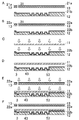
- a and B are schematic diagrams for explaining the configuration of the microchip 1a according to the first embodiment of the present technology. It is a flowchart for demonstrating the manufacturing method of the microchip 1a.
- a to F are schematic views for explaining a method of manufacturing the microchip 1a. It is a schematic diagram for demonstrating the structure of the microchip 1b which concerns on 2nd embodiment of this technique. It is a flowchart for demonstrating the manufacturing method of the microchip 1b.
- a to F are schematic views for explaining a method of manufacturing the microchip 1b. It is a mimetic diagram for explaining the composition of microchip 1c concerning a third embodiment of this art.
- a to F are schematic views for explaining a method of manufacturing the microchip 1c.
- FIG. 1 is a schematic diagram showing a configuration of a microchip 1a according to the first embodiment of the present technology.
- 1A is a schematic top view
- FIG. 1B is a schematic cross-sectional view corresponding to the PP cross section of FIG. 1A.
- the microchip denoted by reference numeral 1a in the figure as an area into which a liquid such as a sample solution is introduced, an introduction part 3 into which the liquid is introduced from the outside, wells 51 to 55 serving as a reaction field for the analyte, Channels 41 to 45 connecting the part 3 and the wells 51 to 55 are provided.
- wells 51 all five wells to which the liquid is supplied by the flow path 41 are referred to as wells 51, and each of the five wells to which the liquid is supplied by the flow paths 42, 43, 44, and 45 This will be described as wells 52, 53, 54, and 55.
- the configuration of the microchip according to the present technology is not limited to the number and arrangement of the introduction unit 3, the flow paths 41 to 45, and the wells 51 to 55 shown in FIG.
- the microchip according to the present technology includes a plurality of substrate layers and a bonding layer made of a silicon compound provided at the interface of the substrate layers. Further, at least one of the bonding layers is made of an organosilicon compound.
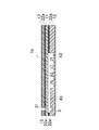
- the microchip 1a according to this embodiment shown in FIG. 1B is composed of, for example, three substrate layers 11, 12, and 13.
- the plurality of substrate layers 11, 12, and 13 constituting the microchip 1a preferably include a substrate layer made of a non-silicone resin and a substrate layer made of polydimethylsiloxane.
- both surfaces of the substrate layer made of polydimethylsiloxane are bonded to the substrate layer made of the first non-silicone resin and the substrate layer made of the second non-silicone resin through the bonding layer.
- the substrate layer made of polydimethylsiloxane is used as the substrate layer 11, and among the two substrate layers bonded to the substrate layer 11, "made of the first non-silicone resin".
- the “substrate layer” is referred to as “substrate layer 12”
- the “substrate layer made of the second non-silicone resin” is referred to as “substrate layer 13”. This is the same in the second embodiment and the third embodiment described later.
- the substrate layer 12 has a groove on the joint surface with the substrate layer 11, and the groove introduces a liquid such as a sample solution in the introduction part 3, the flow paths 41 to 45, and the wells 51 to 55. Corresponds to the area.
- the substrate layer 12 is bonded to the substrate layer 11 via a bonding layer 22b made of a silicon compound.
- the bonding layer 22b is a bonding layer made of an inorganic silicon compound.
- the substrate layer 13 does not have a groove on the bonding surface with the substrate layer 11, and the substrate layer 13 is bonded to the substrate layer 11 via the bonding layer 22a made of an organosilicon compound.
- the region where the liquid such as the introduction portion 3 provided in the microchip 1a is introduced is microscopic. There is no communication with the outside of the chip 1a.
- the substrate layer 11 is made of a material having elasticity, a part of the puncture member such as a needle can be penetrated from the outside of the microchip 1a to the introduction portion 3 while overlooking the introduction port 31 formed in the substrate layer 13. Is possible.
- the liquid can be introduced into a region such as the introduction portion 3 in the microchip 1a. Further, since the sealed region is connected only to the inside of the syringe by the penetration of the substrate layer 11 with a needle or the like, the liquid can be introduced without bubbles entering the flow paths 41 to 45 and the wells 51 to 55. Can do.
- the puncture site can be naturally sealed by the self-sealing property of the substrate layer 11. .
- self-sealing property of the substrate layer.
- the liquid introduced into the microchip 1a refers to a sample solution or the like containing an analysis object or a substance that reacts with another substance to generate the analysis object.
- the analysis target include nucleic acids such as DNA and RNA, proteins including peptides, antibodies, and the like.
- the biological sample itself containing the said analysis target object, such as blood, or its diluted solution can also be made into the liquid introduce
- an analysis method using the microchip 1a for example, an analysis method using a nucleic acid amplification reaction such as a conventional PCR (Polymerase Chain Reaction) method in which a temperature cycle is performed and various isothermal amplification methods without a temperature cycle are used. included.
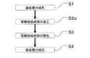
- symbol S ⁇ b> 1 is a step of forming a substrate layer.
- this step grooves corresponding to the introduction portion 3, the channels 41 to 45 and the wells 51 to 55 and a hole corresponding to the introduction port 31 are formed in the substrate layer 12.
- Glass, plastics, metals, ceramics, and the like can be adopted as the material for the substrate layers 12 and 13, but plastics are particularly preferable.
- the substrate layers 12 and 13 are preferably made of a material having gas impermeability.
- Gas impermeable plastics include PMMA (polymethyl methacrylate: acrylic resin), PC (polycarbonate), PS (polystyrene), PP (polypropylene), PE (polyethylene), PET (polyethylene terephthalate), diethylene glycol bis.
- PMMA polymethyl methacrylate: acrylic resin
- PC polycarbonate
- PS polystyrene
- PP polypropylene
- PE polyethylene
- PET polyethylene terephthalate
- diethylene glycol bis diethylene glycol bis.
- non-silicone resins such as acrylic resin and PC are preferable.
- the material of the substrate layers 11, 12, and 13 is light transmissive and has little autofluorescence and wavelength dispersion. Therefore, it is preferable to select a material having a small optical error because of a small value.
- the formation of the introduction portion 3 and the like on the substrate layers 12 and 13 can be performed by a known method. For example, wet etching or dry etching of a glass substrate layer, or nanoimprint, injection molding or cutting of a plastic substrate layer.
- the microchip 1a is not limited to the configuration shown in FIG. The remaining portion may be formed on the substrate layer 12.
- the substrate layer forming step S1 is not an essential step, and substrate layers 12 and 13 in which grooves and holes are formed in advance are separately prepared. It can also carry out from lamination process S2 of a crosslinkable composition to layers 12 and 13.
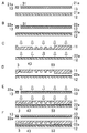
- FIG. 3 is a figure which shows typically each process from this process to joining process S4 of a substrate layer.
- a crosslinkable composition 21b containing a silicon compound is laminated on the substrate layer 12, and a crosslinkable composition 21a containing a silicon compound is laminated on the substrate layer 13.
- a crosslinkable composition 21a containing an organosilicon compound is applied to the surface of the substrate layer 13 in which only holes corresponding to the introduction port 31 are formed, and no groove is provided (crosslinkable composition).
- a crosslinkable composition 21b containing a silicon compound is vapor-deposited on the groove forming surface of the substrate layer 12 on which grooves corresponding to the introduction part 3 and the like are formed (deposition step S2b of the crosslinkable composition).
- the crosslinkable composition containing a silicon compound used in the manufacturing process of the microchip 1a is, for example, a condensate containing silanol groups generated by hydrolysis and partial condensation of alkoxysilanes, and the condensate is an alcohol. It may be dispersed in a liquid such as a solvent.
- the crosslinkable composition 21a used in the coating step S2a preferably contains an organosilicon compound.
- the crosslinkable composition containing an organosilicon compound is obtained, for example, by adding a condensate of an alkoxysilane containing an organic functional group to a solvent in which a condensate containing a silanol group is dispersed.
- colloidal silica and the like may be added to the crosslinkable composition containing the organosilicon compound.
- the crosslinkable composition 21a containing a silicon compound used in this step can be a commercially available silicone hard coat agent or the like.
- a hard coat agent “NSC-1600” manufactured by Nippon Seika Co., Ltd. can be used.
- a hard coat agent “NSC-2705” manufactured by Nippon Seika Co., Ltd. can be used.
- crosslinkable composition 21a containing the organosilicon compound to the substrate layer 13 can be performed by a known method. For example, dipping coat, spray coat, flow coat, spin coat and the like. As long as the coating method is such that the organic chain contained in the crosslinkable composition 21a is retained, an appropriate method may be selected according to the characteristics and shape of the material of the substrate layer 13, and the coating method is particularly limited. Not.
- the crosslinkable composition 21b used in the vapor deposition step S2b also contains a silicon compound, but is not limited to a condensate containing an organosilicon compound, and is a condensate containing a silicon compound containing no organic chain. Also good.
- a silicon compound that does not contain an organic chain is referred to as an “inorganic silicon compound”.
- Examples of the crosslinkable composition 21b include a solution containing a condensate of alkoxysilanes such as a polysiloxane oligomer.
- the vapor deposition onto the substrate layer 12 of the crosslinkable composition 21b containing an inorganic silicon compound can be performed by a known method. For example, vacuum deposition, ion plating, sputtering and the like. From these methods, an appropriate method may be selected according to the characteristics and shape of the material of the substrate layer 13, and the deposition method is not particularly limited.
- the crosslinkable compositions 21a and 21b are applied or vapor-deposited only on the surfaces of the substrate layers 12 and 13 in contact with the substrate layers 11, The crosslinkable compositions 21a and 21b may be applied or vapor-deposited on other portions of the substrate layers 12 and 13.
- the microchip 1a according to the first embodiment of the present technology whether or not the crosslinkable compositions 21a and 21b are applied to the substrate layers 12 and 13 other than the bonding surfaces with the respective substrate layers 11 or whether or not vapor deposition is performed.
- the crosslinkable composition 21 a and 21b are applied or vapor-deposited on the outer surface of the microchip 1a, the crosslinkable compositions 21a and 21b are cured by the curing treatment of the crosslinkable compositions 21a and 21b, which will be described later.
- the outer surface of 1a is covered with a layer formed by curing the crosslinkable compositions 21a and 21b. By covering with this layer, the outer surface of the microchip 1a is less likely to be damaged, and the durability of the microchip 1a is improved.
- symbol S3 is the process of superposing
- this step is a step of polymerizing the crosslinkable compositions 21a and 21b to form the bonding layers 22a and 22b.
- Silanol groups contained in the crosslinkable compositions 21a and 21b are condensed by heating to form siloxane bonds (Si—O—Si).
- the layers formed by curing the crosslinkable compositions 21a and 21b including the siloxane bond are the bonding layers 22a and 22b.
- the heating temperature is determined according to the material of each of the substrate layers 12 and 13. Good.
- the heating temperature is preferably 80 to 120 ° C. when PC is used for the substrate layers 12 and 13, for example, and 60 to 80 ° C. is preferable when PMMA is used.
- symbol S4 is a bonding step of the substrate layer.
- the groove-formed surface (surface on which the region is formed) of the substrate layer 12 coated with the crosslinkable composition 21b containing the silicon compound and the substrate coated with the crosslinkable composition 21a containing the organosilicon compound This is a bonding step in which the surface of the layer 13 on which the groove is not provided is bonded to the substrate layer 11.
- the substrate layer 12 is bonded to the substrate layer 11, and then the substrate layer 11 and the substrate layer 13 are bonded.
- the order of bonding of the substrate layers 11, 12, 13 may start from the bonding of the substrate layer 11 and the substrate layer 13.
- the substrate layer 11 is preferably made of a silicone resin capable of forming a siloxane bond with the bonding layers 22a and 22b because the bonding layers 22a and 22b stacked on the substrate layers 12 and 13 contain siloxane bonds. Further, a silicone elastomer having elasticity is suitable for the substrate layer 11, and for example, polydimethylsiloxane (PDMS) is desirable.
- PDMS polydimethylsiloxane
- the plurality of substrate layers constituting the microchip include the substrate layers 12 and 13 that are the above-described substrate layers made of non-silicone resin, the substrate layer 11 that is made of PDMS, It is preferable that both surfaces of the substrate layer made of PDMS are bonded to the substrate layers (substrate layers 12 and 13) each made of a non-silicone resin via bonding layers 22a and 22b.
- This preferred configuration is the same for the second and third embodiments described later.
- activation processing is performed on the surface of the substrate layer 12 on which the bonding layer 22 b is provided and one surface of the substrate layer 11.
- the activation treatment can be performed by irradiating oxygen plasma or ultraviolet rays, and other known methods such as ion beam irradiation may be used.
- OH group bonds are generated on the surface of the bonding layer 22b on the substrate layer 12.
- the substrate layer 11 is made of a silicone resin
- OH group bonds are generated on the surface subjected to the activation treatment. Bonds of OH groups generated in the substrate layer 11 and the bonding layer 22b are highly reactive.
- the groove in the substrate layer 12 corresponding to the region such as the introduction portion 3 The sky can be hermetically sealed so as to be a negative pressure (1/100 atm) with respect to the atmospheric pressure.
- the liquid is automatically sucked by the negative pressure inside the microchip 1a when the liquid is introduced, and a fine channel structure is formed.
- the liquid can be introduced into the microchip 1a in a shorter time.
- the material of the substrate layers 12 and 13 is preferably gas-impermeable. Even if the microchip 1a is stored in the atmosphere, the substrate layers 12 and 13 constituting the outer surface of the microchip 1a are made of a material having gas impermeability such as PC. The region is held at negative pressure. Further, when the substrate layers 12 and 13 are made of a gas-impermeable material, the liquid introduced into the wells 51 to 55 is vaporized by heating even when the microchip 1a is heated in the analysis process. Further, it is possible to prevent disappearance (liquid loss) through the substrate layer 11.
- the bonding between the substrate layer 13 and the substrate layer 11 is performed by activating the surfaces of the bonding layer 22a and the substrate layer 11 (FIG. 3E), generating OH groups on the treated surface, and then processing each other.
- the surfaces are pasted together (FIG. 3F).
- the substrate layer 11 is bonded to the surface of the substrate layer 13 where the groove is not formed via the bonding layer 22a made of an organosilicon compound.
- the bonding layers 22a and 22b containing a silicon compound are provided on the bonding surfaces of the substrate layers 11, 12, and 13 and bonded via siloxane bonds.
- the substrate layers 11, 12, and 13 can be firmly bonded. Therefore, a structure such as a fine channel formed in the substrate layer can be reliably sealed.
- a siloxane bond can be formed and a strong bonded state can be obtained without using a glass substrate layer.
- the microchip 1a is less likely to be damaged than a microchip using a glass substrate layer. Further, by not using the glass substrate layer, the microchip 1a can be reduced in weight.
- the bonding layers 22a and 22b in the microchip 1a have the effect of increasing the strength of the microchip 1a itself, in addition to the effect of strengthening the bonding of the substrate layers 11, 12, and 13. Since the bonding layers 22a and 22b are sandwiched between the substrate layers 11, 12, and 13, deformation of the microchip 1a is prevented.
- at least one bonding layer 22a of the microchip 1a is made of an organosilicon compound, it is more flexible and less susceptible to cracking than a bonding layer made of a silicon compound that does not contain an organic chain, and the durability of the microchip 1a is improved. Improve.
- FIG. 4 is a schematic cross-sectional view showing the configuration of a microchip 1b according to the second embodiment of the present technology.
- the microchip 1b has the same configuration as that of the first embodiment except for the bonding layer 22a provided at the interface between the substrate layer 11 and the substrate layer 12.
- the same components as those in the first embodiment are denoted by the same reference numerals, and description thereof is omitted.
- the material of the substrate layers 11, 12, 13 constituting the microchip 1b is the same as that of the substrate layer having the same reference numeral in the microchip 1a.
- the bonding layer is formed on the interface between the substrate layer 11 and the surface on which the groove corresponding to the region such as the introduction portion 3 of the substrate layer 12 is formed, as well as the interface between the substrate layer 11 and the substrate layer 13. 22a is provided.
- microchip Manufacturing Method According to Second Embodiment of the Present Technology
- a microchip 1b manufacturing method will be described with reference to a flowchart shown in FIG.
- the manufacturing process of the microchip 1b the forming process S1 of the substrate layer, the curing process S3 of the crosslinkable composition, and the bonding process S4 of the substrate layer are the same as the manufacturing process of the microchip 1a according to the first embodiment. . Therefore, a cross-linking composition coating step S2a different from the microchip 1a manufacturing step will be described with reference to FIG.
- crosslinkable composition 21a containing an organosilicon compound.
- the crosslinkable composition 21a that covers the substrate layers 12 and 13 both contains an organosilicon compound.
- the method for applying the crosslinkable composition 21a containing the organosilicon compound to each of the substrate layers 12 and 13 is the same as the method described in the first embodiment. Further, in the coating step S2a of the crosslinkable composition 21a on the substrate layer 12, the coating was performed only on the portion of the substrate layer 12 that was in contact with the substrate layer 11.
- masking may be performed on the uncoated portion of the substrate layer 12 before coating (the masking layer is not shown in FIG. 6A). ).
- a water-soluble resist can be used for the masking.
- the portion of the substrate layer 12 where the wells and the like are formed is covered with a water-soluble resist, and the crosslinkable compound 21 a is applied to the substrate layer 12.
- the water-soluble resist is removed from the substrate layer 12 using, for example, water.
- a technique such as ultrasonic waves may be used in combination.
- a metal thin film may also be used for masking.
- a metal such as aluminum is coated on the substrate layer 12 with a thickness of about 100 nm by vapor deposition or sputtering.
- the removal of the metal thin film from the substrate layer 12 is performed using, for example, an alkaline aqueous solution.
- the metal thin film is peeled off from the substrate layer 12 by using a technique such as ultrasonic waves in combination.
- the part which masks is not limited to the area
- dipping coat is selected as the coating method of the crosslinkable composition 21a and the crosslinkable composition 21a is not applied to one surface of the substrate layer 12 disposed on the outer surface of the microchip 1b, this surface is used. Can be masked.
- crosslinkable composition 21a may be partially applied to the substrate layer 12 by precision screen printing or the like without masking the substrate layer 12.
- the bonding layer 22a may be formed in a region where the liquid is introduced, such as the introduction portion 3, as in the microchip 1a according to the first embodiment.
- the presence or absence of application of the crosslinkable composition 21a to the groove portion of the substrate layer 12 is not particularly limited as long as the sample solution and the analysis using the microchip 1b are not affected.
- the microchip 1a which concerns on 1st embodiment and the microchip 1c which concerns on 3rd embodiment mentioned later are also the same.
- the crosslinkable composition containing the organosilicon compound covering the substrate layer 12 and the crosslinkable composition containing the organosilicon compound covering the substrate layer 13 are both denoted by reference numeral 21a.
- the composition of the crosslinkable composition covering each of the substrate layers 12 and 13 need not be the same.
- a crosslinkable composition 21a containing an appropriate organosilicon compound may be selected in accordance with each material.
- the crosslinkable composition 21a containing an organosilicon compound is superposed
- the bonding layer 22a provided on the substrate layer 12 and one surface of the substrate layer 11 made of a silicone resin such as polydimethylsiloxane are activated (FIG. 6C).
- the layer 11 and the substrate layer 12 are bonded together (FIG. 6D).
- the activation process is performed on the bonding layer 22 a provided on the substrate layer 13 and the other surface of the substrate layer 11 (FIG. 6E), and the substrate layer 11 and the substrate layer 13 are bonded together. (FIG. 6F).
- a bonding layer 22a containing a silicon compound is provided on each bonding surface of the substrate layers 11, 12, and 13, thereby providing a substrate.
- the layers 11, 12, 13 can be firmly bonded.
- the bonding layers 22a and 22a laminated on the substrate layer 12 and the substrate layer 13 in the microchip 1b both contain an organic silicon compound, the bonding layers 22a and 22a are flexible and hardly crack, and are compared with a bonding layer that does not include an organic chain. Therefore, it is more difficult to peel off from the substrate layers 11, 12, and 13, and the durability of the microchip 1b is improved.
- FIG. 7 is a schematic cross-sectional view showing the configuration of a microchip 1c according to the third embodiment of the present technology.
- the substrate layer 11 has a groove on the joint surface with the substrate layer 12.
- the substrate layers 12 and 13 are bonded to the substrate layer 11 via bonding layers made of an organosilicon compound. That is, unlike the microchip 1a according to the first embodiment and the microchip 1b according to the second embodiment, the microchip 1c has a region where a liquid such as the introduction portion 3 is introduced into the substrate layer 11. Other configurations are the same as those of the microchip 1b.
- microchip 1b The same components as those of the microchip 1b are denoted by the same reference numerals, and description thereof is omitted. Further, the material of the substrate layers 11, 12, and 13 constituting the microchip 1c is the same as the substrate layer denoted by the same reference numeral in the microchip 1a according to the first embodiment.
- the microchip manufacturing method according to the third embodiment of the present technology The manufacturing method of the microchip 1c is the same as the manufacturing process of the microchip 1b according to the second embodiment, and thus the flowchart is omitted.
- a substrate layer forming step S1 and a crosslinkable composition coating step S2a, which are partially different from the manufacturing steps of the microchip 1b, will be described with reference to FIG.
- a groove corresponding to a region such as the introduction portion 3 is formed in the substrate layer 11 made of a silicone resin such as polydimethylsiloxane. Therefore, as shown in FIG. 8A, the substrate layer 12 and the substrate layer 13 are formed with the inlet 31 but not with the unevenness of the wells 51 to 55 and the like.
- a crosslinkable composition 21a containing an organosilicon compound is applied to each of the substrate layers 12 and 13 (FIG. 8A).
- the crosslinkable composition 21a covering the substrate layers 12 and 13 contains an organosilicon compound.
- the method of applying the crosslinkable composition 21a containing the organosilicon compound to each of the substrate layers 12 and 13 is the same as the method mentioned in the method for manufacturing the microchip 1a.
- the composition of the crosslinkable compositions 21a and 21a containing the organosilicon compound that covers the substrate layers 12 and 13 is not necessarily the same.
- the substrate layers 12 and 13 coated with the crosslinkable composition 21a containing the organosilicon compound polymerize the crosslinkable compositions 21a and 21a containing the organosilicon compound in the curing step S3, as in the manufacturing process of the microchip 1a. Then, the bonding layers 22a and 22a are formed (FIG. 8B). Thereafter, in the substrate layer bonding step S4, the bonding layer 22a provided on the substrate layer 12 and the surface of the substrate layer 11 on which the groove is formed are activated (FIG. 8C), and the substrate layer 11 and the substrate layer 12 are activated. Are pasted together (FIG. 8D).
- an activation process is performed on the bonding layer 22 a provided on the substrate layer 13 and the other surface of the substrate layer 11 (FIG. 8E), and the substrate layer 11 and the substrate layer 13 are bonded together. (FIG. 8F).
- a bonding layer containing a silicon compound is provided on each bonding surface of the substrate layers 11, 12, and 13.
- the bonding layers 22a and 22a of the microchip 1c both contain an organosilicon compound, and are therefore flexible and hardly cracked.
- the crosslinkable composition 21a containing an organic silicon compound which cannot select a method such as vapor deposition, to the substrate layers 12 and 13 because it contains an organic chain.
- a microchip comprising a plurality of substrate layers and a bonding layer made of a silicon compound provided at an interface between the substrate layers, wherein at least one of the bonding layers is made of an organosilicon compound.
- the plurality of substrate layers include a substrate layer made of a non-silicone resin and a substrate layer made of polydimethylsiloxane, and both surfaces of the substrate layer made of polydimethylsiloxane are made of a first non-silicone resin.
- the substrate layer made of the first non-silicone resin has a groove on the joint surface with the substrate layer made of polydimethylsiloxane, and has a groove on the joint surface with the substrate layer made of polydimethylsiloxane.
- the substrate layer made of polydimethylsiloxane has a groove on a joint surface with the substrate layer made of the first non-silicone resin, and the substrate layer made of the first non-silicone resin and the second non-silicone resin.
- the minute structure in the microchip is hermetically sealed, so that a valuable trace sample can be reliably analyzed. Further, the microchip can be reduced in weight by not using the glass substrate layer. For this reason, it becomes easy to carry and the microchip according to the present technology can be used for clinical genotyping and pathogen determination.
- 1a, 1b, 1c Microchip, 11, 12, 13: Substrate layer, 21a, 21b: Crosslinkable composition, 22a, 22b: Bonding layer, 3: Introduction part, 31: Introduction port, 41, 42, 43, 44, 45: channel, 51, 52, 53, 54, 55: well
Abstract
Description
前記複数の基板層は、非シリコーン樹脂からなる基板層と、ポリジメチルシロキサンからなる基板層と、を含み、前記ポリジメチルシロキサンからなる基板層の両面は、第1の非シリコーン樹脂からなる基板層及び第2の非シリコーン樹脂からなる基板層と、前記接合層を介して、接合していてもよい。
また、前記第1の非シリコーン樹脂からなる基板層は前記ポリジメチルシロキサンからなる基板層との接合面に溝を有し、前記ポリジメチルシロキサンからなる基板層との接合面に溝を有していない前記第2の非シリコーン樹脂からなる基板層と、前記ポリジメチルシロキサンからなる基板層とは、前記有機ケイ素化合物からなる接合層を介して接合している、マイクロチップであってもよい。
さらに、前記ポリジメチルシロキサンからなる基板層と、前記第1の非シリコーン樹脂からなる基板層とは、無機ケイ素化合物からなる接合層を介して接合していてもよい。
その他、前記ポリジメチルシロキサンからなる基板層は前記第1の非シリコーン樹脂からなる基板層との接合面に溝を有し、前記第1の非シリコーン樹脂からなる基板層と前記第2の非シリコーン樹脂からなる基板層とが、各々前記ポリジメチルシロキサンからなる基板層と、前記有機ケイ素化合物からなる接合層を介して接合している、マイクロチップであってもよい。
前記第1の非シリコーン樹脂からなる基板層及び第2の非シリコーン樹脂からなる基板層は、アクリル樹脂又はポリカーボネートからなるものであってもよくガス不透過性であってもよい。
さらに、前記ポリジメチルシロキサンからなる基板層は弾性変形による自己封止性を備え、前記溝の内空が大気圧に対して負圧とされていてもよい。
マイクロチップの製造方法には、前記ケイ素化合物を含む架橋性組成物で被覆された、前記第1の非シリコーン樹脂からなる基板層の前記溝形成面と、前記有機ケイ素化合物を含む架橋性組成物で被覆された、前記第2の非シリコーン樹脂からなる基板層の前記溝が設けられていない面と、を各々ポリジメチルシロキサンからなる基板層と、貼り合わせる接合工程を含んでいてもよい。
1.本技術の第一実施形態に係るマイクロチップの構成
2.本技術の第一実施形態に係るマイクロチップの製造方法
(1)基板層の成形
(2)架橋性組成物の積層
(3)架橋性組成物の硬化
(4)基板層の接合
3.本技術の第二実施形態に係るマイクロチップの構成
4.本技術の第二実施形態に係るマイクロチップの製造方法
(1)架橋性組成物の塗工
5.本技術の第三実施形態に係るマイクロチップの構成
6.本技術の第三実施形態に係るマイクロチップの製造方法
(1)基板層の成形
(2)架橋性組成物の塗工
図1は、本技術の第一実施形態に係るマイクロチップ1aの構成を示す模式図である。図1Aは上面模式図であり、図1Bは、図1AのP-P断面に対応する断面模式図である。
マイクロチップ1aの製造方法について、図2に示すフローチャートを参照して説明する。
図2中、符号S1は基板層の成形工程である。本工程では、基板層12に、導入部3、流路41~45、及びウェル51~55に相当する溝と、基板層13に導入口31に相当する孔を成形する。基板層12,13の材料には、ガラス、プラスチック類、金属類及びセラミック類などを採用できるが、特に、プラスチック類が好ましい。また、後述するように、基板層12,13にはガス不透過性を有する材料が好ましい。ガス不透過性を有するプラスチック類としては、PMMA(ポリメチルメタアクリレート:アクリル樹脂)、PC(ポリカーボネート)、PS(ポリスチレン)、PP(ポリプロピレン)、PE(ポリエチレン)、PET(ポリエチレンテレフタレート)、ジエチレングリコールビスアリルカーボネート、SAN樹脂(スチレン-アクリロニトリル共重合体)、MS樹脂(MMA-スチレン共重合体)、TPX(ポリ(4-メチルペンテン-1))、ポリオレフィン、SiMA(シロキサニルメタクリレートモノマー)-MMA共重合体、SiMA-フッ素含有モノマー共重合体、シリコーンマクロマー(A)-HFBuMA(ヘプタフルオロブチルメタクリレート)-MMA3元共重合体、ジ置換ポリアセチレン系ポリマー等が挙げられる。このうち、非シリコーン樹脂である、アクリル樹脂やPCが好適である。
図2中、符号S2(S2a及びS2b)は、基板層12,13への架橋性組成物の積層工程である。また、図3は、本工程から、基板層の接合工程S4までの各工程を模式的に示す図である。図3Aに示すように、本工程では、基板層12にケイ素化合物を含む架橋性組成物21bを、基板層13に、ケイ素化合物を含む架橋性組成物21aを積層する。具体的には、導入口31に相当する孔のみが形成された基板層13の、溝が設けられていない面に、有機ケイ素化合物を含む架橋性組成物21aを塗工し(架橋性組成物の塗工工程S2a)、導入部3等に相当する溝が形成された基板層12の溝形成面に、ケイ素化合物を含む架橋性組成物21bを蒸着する(架橋性組成物の蒸着工程S2b)。
マイクロチップ1aの製造工程で用いる、ケイ素化合物を含む架橋性組成物とは、例えば、アルコキシシラン類が加水分解・部分縮合により生成されたシラノール基を含有する縮合物であり、この縮合物がアルコール溶媒などの液体に分散されている状態であってもよい。塗工工程S2aにおいて用いる架橋性組成物21aは、有機ケイ素化合物を含むものが好ましい。有機ケイ素化合物を含む架橋性組成物は、例えば、先のシラノール基を含有する縮合物が分散された溶媒に、有機官能基を含むアルコキシシランの縮合物が加えられたものである。具体的には、例えば、アルキルトリアルコキシシランとテトラアルコキシシランとの縮合物が含まれる溶媒などである。この他、有機ケイ素化合物を含む架橋性組成物には、上記の縮合物の他、コロイド状のシリカなどが添加されていてもよい。
一方、蒸着工程S2bで用いる架橋性組成物21bも、ケイ素化合物が含まれているが、有機ケイ素化合物を含む縮合物には限定されず、有機鎖を含まないケイ素化合物を含む縮合物であってもよい。本実施形態では、有機鎖を含まないケイ素化合物を、「無機ケイ素化合物」と称する。架橋性組成物21bとしては、例えば、ポリシロキサンオリゴマーなどのアルコキシシラン類の縮合物を含む溶液などが挙げられる。
図2中、符号S3は架橋性組成物を重合して硬化する工程である。本工程では、図3A及び図3Bに示すように、基板層12,13に積層された架橋性組成物21a,21bを加熱して、硬化させる。すなわち、本工程は、架橋性組成物21a,21bを重合させて接合層22a,22bを形成させる工程である。架橋性組成物21a,21bに含まれるシラノール基が加熱により縮合し、シロキサン結合(Si-O-Si)が形成される。このシロキサン結合を含む、架橋性組成物21a,21bが硬化して形成された層が、接合層22a,22bである。
図2中、符号S4は基板層の接合工程である。本工程では、ケイ素化合物を含む架橋性組成物21bで被覆された基板層12の溝形成面(領域が形成された面)と、有機ケイ素化合物を含む架橋性組成物21aで被覆された、基板層13の溝が設けられていない面とを、基板層11と貼り合わせる接合工程である。具体的には、例えば、基板層11に基板層12を貼り合わせ、次いで基板層11と基板層13とを貼り合わせる。基板層11,12,13の貼り合わせの順序は、基板層11と基板層13との接合から始めてもよい。
図4は、本技術の第二実施形態に係るマイクロチップ1bの構成を示す断面模式図である。マイクロチップ1bは、基板層11と基板層12の界面に設けられる接合層22a以外の構成については、第一実施形態と同一である。第一実施形態と同一の構成については、同一の符号を付し、説明については省略する。また、マイクロチップ1bを構成する基板層11,12,13の材料は、マイクロチップ1aにおいて同一の符号を付した基板層と同じである。マイクロチップ1bでは、基板層12の導入部3等の領域に相当する溝が形成された面と基板層11との界面にも、基板層11と基板層13の界面と同じように、接合層22aが設けられている。
マイクロチップ1bの製造方法について、図5に示すフローチャートを参照して説明する。マイクロチップ1bの製造工程では、基板層の成形工程S1、架橋性組成物の硬化工程S3、及び基板層の接合工程S4については、第一実施形態に係るマイクロチップ1aの製造工程と同様である。そこで、マイクロチップ1aの製造工程と異なる架橋性組成物の塗工工程S2aについて、図6を参照して説明する。
本工程では、図6Aに示すように、基板層12の導入部3等の領域に相当する溝が形成されている面と、基板層13の一の面に、各々、有機ケイ素化合物を含む架橋性組成物21aを塗工する。本実施形態では、基板層12,13を被覆する架橋性組成物21aは、何れも有機ケイ素化合物を含んでいる。有機ケイ素化合物を含む架橋性組成物21aの、各基板層12,13への塗工方法は、第一実施形態において挙げた手法と同様である。また、基板層12への架橋性組成物21aの塗工工程S2aでは、基板層12において基板層11と接する部分のみに塗工した。
図7は、本技術の第三実施形態に係るマイクロチップ1cの構成を示す断面模式図である。マイクロチップ1cにおいては、基板層11は、基板層12との接合面に溝を有している。また、基板層12,13は、各々基板層11と有機ケイ素化合物からなる接合層を介して接合している。すなわち、マイクロチップ1cは、第一実施形態に係るマイクロチップ1a及び第二実施形態に係るマイクロチップ1bと異なり、基板層11に導入部3等の液体が導入される領域が形成されている。その他の構成については、マイクロチップ1bと同一である。マイクロチップ1bと同一の構成については、同一の符号を付し、説明については省略する。また、マイクロチップ1cを構成する基板層11,12,13の材料は、第一実施形態に係るマイクロチップ1aにおいて同一の符号を付した基板層と同じである。
マイクロチップ1cの製造方法については、第二実施形態に係るマイクロチップ1bの製造工程と同一の製造工程であるため、フローチャートは省略する。マイクロチップ1bの製造工程と一部異なる、基板層の成形工程S1と架橋性組成物の塗工工程S2aについては、図8を参照して説明する。
基板層の成形工程S1では、ポリジメチルシロキサンなどのシリコーン樹脂からなる基板層11に、導入部3などの領域に相当する溝を成形する。そのため、図8Aに示すように、基板層12及び基板層13には、導入口31は成形されるものの、ウェル51~55等の凹凸が成形されない。
架橋性組成物の塗工工程S2aでは、基板層12,13の各々一の面に、有機ケイ素化合物を含む架橋性組成物21aを塗工する(図8A)。マイクロチップ1cの製造工程においても、第二実施形態に係るマイクロチップ1bと同様に、基板層12,13を被覆する架橋性組成物21aは何れも、有機ケイ素化合物を含んでいる。有機ケイ素化合物を含む架橋性組成物21aの各基板層12,13への塗工方法は、マイクロチップ1aの製造方法において挙げた手法と同様である。なお、各基板層12,13を被覆する有機ケイ素化合物を含む架橋性組成物21a,21aの組成は、同一である必要はない。
(1)複数の基板層と、前記基板層の界面に設けられた、ケイ素化合物からなる接合層とからなり、前記接合層のうち少なくとも1つは有機ケイ素化合物からなる、マイクロチップ。
(2)前記複数の基板層は、非シリコーン樹脂からなる基板層と、ポリジメチルシロキサンからなる基板層と、を含み、前記ポリジメチルシロキサンからなる基板層の両面は、第1の非シリコーン樹脂からなる基板層及び第2の非シリコーン樹脂からなる基板層と、前記接合層を介して、接合している、上記(1)記載のマイクロチップ。
(3)前記第1の非シリコーン樹脂からなる基板層は前記ポリジメチルシロキサンからなる基板層との接合面に溝を有し、前記ポリジメチルシロキサンからなる基板層との接合面に溝を有していない前記第2の非シリコーン樹脂からなる基板層と、前記ポリジメチルシロキサンからなる基板層とは、前記有機ケイ素化合物からなる接合層を介して接合している、上記(2)記載のマイクロチップ。
(4)前記ポリジメチルシロキサンからなる基板層と、前記第1の非シリコーン樹脂からなる基板層とは、無機ケイ素化合物からなる接合層を介して接合している、上記(3)記載のマイクロチップ。
(5)前記ポリジメチルシロキサンからなる基板層は前記第1の非シリコーン樹脂からなる基板層との接合面に溝を有し、前記第1の非シリコーン樹脂からなる基板層と前記第2の非シリコーン樹脂からなる基板層とが、各々前記ポリジメチルシロキサンからなる基板層と、前記有機ケイ素化合物からなる接合層を介して接合している、上記(2)記載のマイクロチップ。
(6)前記第1の非シリコーン樹脂からなる基板層及び第2の非シリコーン樹脂からなる基板層は、アクリル樹脂又はポリカーボネートからなる、上記(2)~(5)の何れかに記載のマイクロチップ。
(7)前記第1の非シリコーン樹脂からなる基板層及び第2の非シリコーン樹脂からなる基板層は、ガス不透過性である、上記(2)~(6)の何れかに記載のマイクロチップ。
(8)前記ポリジメチルシロキサンからなる基板層は弾性変形による自己封止性を備え、前記溝の内空が大気圧に対して負圧とされている、上記(2)~(7)の何れかに記載のマイクロチップ。
Claims (10)
- 複数の基板層と、
前記基板層の界面に設けられた、ケイ素化合物からなる接合層とからなり、
前記接合層のうち少なくとも1つは有機ケイ素化合物からなる、
マイクロチップ。 - 前記複数の基板層は、非シリコーン樹脂からなる基板層と、ポリジメチルシロキサンからなる基板層と、を含み、
前記ポリジメチルシロキサンからなる基板層の両面は、第1の非シリコーン樹脂からなる基板層及び第2の非シリコーン樹脂からなる基板層と、前記接合層を介して、接合している、
請求項1記載のマイクロチップ。 - 前記第1の非シリコーン樹脂からなる基板層は前記ポリジメチルシロキサンからなる基板層との接合面に溝を有し、
前記ポリジメチルシロキサンからなる基板層との接合面に溝を有していない前記第2の非シリコーン樹脂からなる基板層と、前記ポリジメチルシロキサンからなる基板層とは、前記有機ケイ素化合物からなる接合層を介して接合している、
請求項2記載のマイクロチップ。 - 前記ポリジメチルシロキサンからなる基板層と、
前記第1の非シリコーン樹脂からなる基板層とは、
無機ケイ素化合物からなる接合層を介して接合している、
請求項3記載のマイクロチップ。 - 前記ポリジメチルシロキサンからなる基板層は前記第1の非シリコーン樹脂からなる基板層との接合面に溝を有し、
前記第1の非シリコーン樹脂からなる基板層と前記第2の非シリコーン樹脂からなる基板層とが、各々前記ポリジメチルシロキサンからなる基板層と、前記有機ケイ素化合物からなる接合層を介して接合している、
請求項2記載のマイクロチップ。 - 前記第1の非シリコーン樹脂からなる基板層及び第2の非シリコーン樹脂からなる基板層は、アクリル樹脂又はポリカーボネートからなる、
請求項4記載のマイクロチップ。 - 前記第1の非シリコーン樹脂からなる基板層及び第2の非シリコーン樹脂からなる基板層は、ガス不透過性である、
請求項6記載のマイクロチップ。 - 前記ポリジメチルシロキサンからなる基板層は弾性変形による自己封止性を備え、
前記溝の内空が大気圧に対して負圧とされている、
請求項7記載のマイクロチップ。 - 溝が設けられた第1の非シリコーン樹脂からなる基板層の溝形成面をケイ素化合物を含む架橋性組成物で被覆する蒸着工程と、
第2の非シリコーン樹脂からなる基板層の溝が設けられていない面を有機ケイ素化合物を含む架橋性組成物で被覆する塗工工程と、
を含む、
マイクロチップの製造方法。 - 前記ケイ素化合物を含む架橋性組成物で被覆された、前記第1の非シリコーン樹脂からなる基板層の前記溝形成面と、
前記有機ケイ素化合物を含む架橋性組成物で被覆された、前記第2の非シリコーン樹脂からなる基板層の前記溝が設けられていない面と、を
各々ポリジメチルシロキサンからなる基板層と、貼り合わせる接合工程を含む、
請求項9記載のマイクロチップの製造方法。
Priority Applications (6)
| Application Number | Priority Date | Filing Date | Title |
|---|---|---|---|
| SG11201500017YA SG11201500017YA (en) | 2012-07-09 | 2013-05-09 | Microchip and method for producing manufacturing the same |
| EP18176114.9A EP3388841B1 (en) | 2012-07-09 | 2013-05-09 | Microchip and method for manufacturing the same |
| CN201380035497.4A CN104412110A (zh) | 2012-07-09 | 2013-05-09 | 微芯片和用于制造微芯片的方法 |
| EP13817319.0A EP2871482B1 (en) | 2012-07-09 | 2013-05-09 | Microchip and method for producing microchip |
| JP2014524677A JP6361503B2 (ja) | 2012-07-09 | 2013-05-09 | マイクロチップ及びマイクロチップの製造方法 |
| US14/408,498 US20150239217A1 (en) | 2012-07-09 | 2013-05-09 | Microchip and method for manufacturing the same |
Applications Claiming Priority (2)
| Application Number | Priority Date | Filing Date | Title |
|---|---|---|---|
| JP2012-153584 | 2012-07-09 | ||
| JP2012153584 | 2012-07-09 |
Publications (1)
| Publication Number | Publication Date |
|---|---|
| WO2014010299A1 true WO2014010299A1 (ja) | 2014-01-16 |
Family
ID=49915774
Family Applications (1)
| Application Number | Title | Priority Date | Filing Date |
|---|---|---|---|
| PCT/JP2013/063054 WO2014010299A1 (ja) | 2012-07-09 | 2013-05-09 | マイクロチップ及びマイクロチップの製造方法 |
Country Status (6)
| Country | Link |
|---|---|
| US (1) | US20150239217A1 (ja) |
| EP (2) | EP3388841B1 (ja) |
| JP (2) | JP6361503B2 (ja) |
| CN (1) | CN104412110A (ja) |
| SG (1) | SG11201500017YA (ja) |
| WO (1) | WO2014010299A1 (ja) |
Cited By (1)
| Publication number | Priority date | Publication date | Assignee | Title |
|---|---|---|---|---|
| WO2018109829A1 (ja) * | 2016-12-13 | 2018-06-21 | 栄研化学株式会社 | マイクロチップ |
Families Citing this family (4)
| Publication number | Priority date | Publication date | Assignee | Title |
|---|---|---|---|---|
| CN106391153B (zh) * | 2016-11-07 | 2019-04-09 | 华南理工大学 | 一种负压引导的微流体自律运动的微流控芯片 |
| CN106914286A (zh) * | 2017-01-12 | 2017-07-04 | 上海小海龟科技有限公司 | 一种生物芯片及其封装方法 |
| WO2021038049A1 (en) * | 2019-08-29 | 2021-03-04 | Astraveus | Apparatus and method for clamping a microfluidic device |
| CN115414971B (zh) * | 2022-08-03 | 2023-11-17 | 南方科技大学 | 微控流芯片的制备方法及微控流芯片 |
Citations (4)
| Publication number | Priority date | Publication date | Assignee | Title |
|---|---|---|---|---|
| JP2001519907A (ja) * | 1997-04-04 | 2001-10-23 | アクレイラ バイオサイエンシズ | 包囲されたマイクロチャネル構造体の製造方法 |
| JP2005257283A (ja) * | 2004-03-09 | 2005-09-22 | Fluidware Technologies Kk | マイクロチップ |
| WO2007055151A1 (ja) * | 2005-11-11 | 2007-05-18 | Konica Minolta Medical & Graphic, Inc. | マイクロリアクタおよびマイクロ分析システム |
| JP2011163984A (ja) | 2010-02-10 | 2011-08-25 | Sony Corp | マイクロチップ及びマイクロチップの製造方法 |
Family Cites Families (17)
| Publication number | Priority date | Publication date | Assignee | Title |
|---|---|---|---|---|
| US6825047B1 (en) * | 1996-04-03 | 2004-11-30 | Applera Corporation | Device and method for multiple analyte detection |
| JP2002055030A (ja) * | 2000-08-10 | 2002-02-20 | Sanyo Electric Co Ltd | 半導体装置の解析方法 |
| JP3933058B2 (ja) * | 2002-02-25 | 2007-06-20 | 日立化成工業株式会社 | マイクロ流体システム用支持ユニット及びその製造方法 |
| JP2004325153A (ja) * | 2003-04-23 | 2004-11-18 | Aida Eng Ltd | マイクロチップ及びその製造方法 |
| EP1785457A4 (en) * | 2004-09-03 | 2012-12-19 | Jsr Corp | COATING COMPOSITION, UNDERCOATING COMPOSITION, MULTILAYER BODY WITH COATING FILM OF SUCH A COMPOSITION, PHOTOCATALYZER COATING FILM AND MOLDED BODY |
| EP1885839B1 (en) * | 2005-04-26 | 2018-08-08 | Life Technologies Corporation | Systems and methods for multiple analyte detection |
| EP1900513B1 (en) * | 2005-06-17 | 2012-04-11 | Richell Corporation | Joint structure |
| EP2537657A3 (en) * | 2005-08-09 | 2016-05-04 | The University of North Carolina At Chapel Hill | Methods and materials for fabricating microfluidic devices |
| JP4998462B2 (ja) * | 2006-03-29 | 2012-08-15 | 日本ゼオン株式会社 | 樹脂複合成形体の製造方法 |
| US20080014532A1 (en) * | 2006-07-14 | 2008-01-17 | 3M Innovative Properties Company | Laminate body, and method for manufacturing thin substrate using the laminate body |
| GR1006447B (el) * | 2006-09-15 | 2009-06-19 | Εθνικο Κεντρο Ερευνας Φυσικων Επιστημων (Εκεφε) "Δημοκριτος" | Μεθοδος συγκολλησης |
| JP4992123B2 (ja) * | 2006-12-01 | 2012-08-08 | コニカミノルタアドバンストレイヤー株式会社 | マイクロチップ基板の接合方法、及びマイクロチップ |
| JP2008175795A (ja) * | 2006-12-21 | 2008-07-31 | Sumitomo Bakelite Co Ltd | プラスチック製マイクロチップ、及びその製造方法、並びにそれを利用したバイオチップ又はマイクロ分析チップ |
| US8293061B2 (en) * | 2008-03-06 | 2012-10-23 | University Of Maryland College Park | Low temperature polymer bonding using UV/ozone surface treatment |
| JP5279825B2 (ja) * | 2008-04-22 | 2013-09-04 | アルプス電気株式会社 | 接合部材及びその製造方法 |
| WO2010101044A1 (ja) * | 2009-03-03 | 2010-09-10 | コニカミノルタオプト株式会社 | マイクロチップ用カバー部材、マイクロチップ用カバー部材の製造方法、マイクロチップ、及びマイクロチップの製造方法 |
| JPWO2011122215A1 (ja) * | 2010-03-31 | 2013-07-08 | コニカミノルタ株式会社 | マイクロチップの製造方法及びマイクロチップ |
-
2013
- 2013-05-09 SG SG11201500017YA patent/SG11201500017YA/en unknown
- 2013-05-09 JP JP2014524677A patent/JP6361503B2/ja active Active
- 2013-05-09 CN CN201380035497.4A patent/CN104412110A/zh active Pending
- 2013-05-09 EP EP18176114.9A patent/EP3388841B1/en active Active
- 2013-05-09 EP EP13817319.0A patent/EP2871482B1/en active Active
- 2013-05-09 US US14/408,498 patent/US20150239217A1/en not_active Abandoned
- 2013-05-09 WO PCT/JP2013/063054 patent/WO2014010299A1/ja active Application Filing
-
2018
- 2018-06-28 JP JP2018122948A patent/JP6627921B2/ja active Active
Patent Citations (4)
| Publication number | Priority date | Publication date | Assignee | Title |
|---|---|---|---|---|
| JP2001519907A (ja) * | 1997-04-04 | 2001-10-23 | アクレイラ バイオサイエンシズ | 包囲されたマイクロチャネル構造体の製造方法 |
| JP2005257283A (ja) * | 2004-03-09 | 2005-09-22 | Fluidware Technologies Kk | マイクロチップ |
| WO2007055151A1 (ja) * | 2005-11-11 | 2007-05-18 | Konica Minolta Medical & Graphic, Inc. | マイクロリアクタおよびマイクロ分析システム |
| JP2011163984A (ja) | 2010-02-10 | 2011-08-25 | Sony Corp | マイクロチップ及びマイクロチップの製造方法 |
Cited By (1)
| Publication number | Priority date | Publication date | Assignee | Title |
|---|---|---|---|---|
| WO2018109829A1 (ja) * | 2016-12-13 | 2018-06-21 | 栄研化学株式会社 | マイクロチップ |
Also Published As
| Publication number | Publication date |
|---|---|
| US20150239217A1 (en) | 2015-08-27 |
| JP2019002932A (ja) | 2019-01-10 |
| EP2871482A4 (en) | 2016-03-09 |
| JPWO2014010299A1 (ja) | 2016-06-20 |
| CN104412110A (zh) | 2015-03-11 |
| SG11201500017YA (en) | 2015-02-27 |
| EP2871482B1 (en) | 2018-07-18 |
| JP6627921B2 (ja) | 2020-01-08 |
| JP6361503B2 (ja) | 2018-07-25 |
| EP3388841B1 (en) | 2019-12-11 |
| EP3388841A1 (en) | 2018-10-17 |
| EP2871482A1 (en) | 2015-05-13 |
Similar Documents
| Publication | Publication Date | Title |
|---|---|---|
| JP6627921B2 (ja) | マイクロチップ | |
| JP5229215B2 (ja) | マイクロチップの製造方法 | |
| JP6353451B2 (ja) | マイクロ化学チップ及び反応装置 | |
| JP6422197B2 (ja) | マイクロ化学チップを製造する方法 | |
| WO2011089892A1 (ja) | 硬質シリコーン樹脂の接着方法、微細構造を有する基板の接合方法および当該接合方法を利用したマイクロ流体デバイスの製造方法 | |
| WO2008004572A1 (fr) | Puce à micro passage et procédé de transfert de fluide | |
| EP2507001A1 (en) | Composite plastic articles | |
| US20170341075A1 (en) | Methods and Apparatus for Coated Flowcells | |
| JPWO2008087800A1 (ja) | マイクロチップの製造方法、及びマイクロチップ | |
| US10099218B2 (en) | Method for manufacturing and/or packaging a chip | |
| WO2008065868A1 (en) | Microchip substrate bonding method and microchip | |
| JP2008224431A (ja) | マイクロチップの製造方法、及びマイクロチップ | |
| KR20150016043A (ko) | 미세유동장치 및 그 제조방법 | |
| Ahn et al. | Solvent-free thermoplastic-poly (dimethylsiloxane) bonding mediated by UV irradiation followed by gas-phase chemical deposition of an adhesion linker | |
| JP2005249540A (ja) | マイクロチップ及びpdms基板と対面基板との貼り合わせ方法 | |
| WO2019187275A1 (ja) | 流体デバイス用複合部材およびその製造方法 | |
| JP5239870B2 (ja) | マイクロチップ、及びマイクロチップの製造方法 | |
| JP5516954B2 (ja) | 微細構造を有する基板の接合方法および当該接合方法を利用したマイクロ流体デバイスの製造方法 | |
| JP4992123B2 (ja) | マイクロチップ基板の接合方法、及びマイクロチップ | |
| KR20140143514A (ko) | 기판접합을 위한 기판표면처리방법 및 기판접합방법 | |
| JP2019055379A (ja) | マイクロ流路チップとその製造方法 | |
| CN110227563B (zh) | Pdms微流控芯片防蒸发的密封方法及pdms微流控芯片 | |
| JP5545255B2 (ja) | マイクロチップ及びその製造方法 | |
| Sachsenheimer et al. | Elisabeth Wilhelm, Christiane Neumann, Kai |
Legal Events
| Date | Code | Title | Description |
|---|---|---|---|
| 121 | Ep: the epo has been informed by wipo that ep was designated in this application |
Ref document number: 13817319 Country of ref document: EP Kind code of ref document: A1 |
|
| WWE | Wipo information: entry into national phase |
Ref document number: 2013817319 Country of ref document: EP |
|
| ENP | Entry into the national phase |
Ref document number: 2014524677 Country of ref document: JP Kind code of ref document: A |
|
| WWE | Wipo information: entry into national phase |
Ref document number: 14408498 Country of ref document: US |
|
| NENP | Non-entry into the national phase |
Ref country code: DE |