WO2014007218A1 - 光選択吸収膜、集熱管および太陽熱発電装置 - Google Patents
光選択吸収膜、集熱管および太陽熱発電装置 Download PDFInfo
- Publication number
- WO2014007218A1 WO2014007218A1 PCT/JP2013/068056 JP2013068056W WO2014007218A1 WO 2014007218 A1 WO2014007218 A1 WO 2014007218A1 JP 2013068056 W JP2013068056 W JP 2013068056W WO 2014007218 A1 WO2014007218 A1 WO 2014007218A1
- Authority
- WO
- WIPO (PCT)
- Prior art keywords
- layer
- absorption film
- light selective
- selective absorption
- metal
- Prior art date
- Legal status (The legal status is an assumption and is not a legal conclusion. Google has not performed a legal analysis and makes no representation as to the accuracy of the status listed.)
- Ceased
Links
Images


Classifications
-
- F—MECHANICAL ENGINEERING; LIGHTING; HEATING; WEAPONS; BLASTING
- F24—HEATING; RANGES; VENTILATING
- F24S—SOLAR HEAT COLLECTORS; SOLAR HEAT SYSTEMS
- F24S10/00—Solar heat collectors using working fluids
- F24S10/70—Solar heat collectors using working fluids the working fluids being conveyed through tubular absorbing conduits
-
- F—MECHANICAL ENGINEERING; LIGHTING; HEATING; WEAPONS; BLASTING
- F24—HEATING; RANGES; VENTILATING
- F24S—SOLAR HEAT COLLECTORS; SOLAR HEAT SYSTEMS
- F24S70/00—Details of absorbing elements
- F24S70/10—Details of absorbing elements characterised by the absorbing material
-
- F—MECHANICAL ENGINEERING; LIGHTING; HEATING; WEAPONS; BLASTING
- F24—HEATING; RANGES; VENTILATING
- F24S—SOLAR HEAT COLLECTORS; SOLAR HEAT SYSTEMS
- F24S70/00—Details of absorbing elements
- F24S70/20—Details of absorbing elements characterised by absorbing coatings; characterised by surface treatment for increasing absorption
- F24S70/225—Details of absorbing elements characterised by absorbing coatings; characterised by surface treatment for increasing absorption for spectrally selective absorption
-
- F—MECHANICAL ENGINEERING; LIGHTING; HEATING; WEAPONS; BLASTING
- F03—MACHINES OR ENGINES FOR LIQUIDS; WIND, SPRING, OR WEIGHT MOTORS; PRODUCING MECHANICAL POWER OR A REACTIVE PROPULSIVE THRUST, NOT OTHERWISE PROVIDED FOR
- F03G—SPRING, WEIGHT, INERTIA OR LIKE MOTORS; MECHANICAL-POWER PRODUCING DEVICES OR MECHANISMS, NOT OTHERWISE PROVIDED FOR OR USING ENERGY SOURCES NOT OTHERWISE PROVIDED FOR
- F03G6/00—Devices for producing mechanical power from solar energy
- F03G6/06—Devices for producing mechanical power from solar energy with solar energy concentrating means
- F03G6/061—Parabolic linear or trough concentrators
-
- Y—GENERAL TAGGING OF NEW TECHNOLOGICAL DEVELOPMENTS; GENERAL TAGGING OF CROSS-SECTIONAL TECHNOLOGIES SPANNING OVER SEVERAL SECTIONS OF THE IPC; TECHNICAL SUBJECTS COVERED BY FORMER USPC CROSS-REFERENCE ART COLLECTIONS [XRACs] AND DIGESTS
- Y02—TECHNOLOGIES OR APPLICATIONS FOR MITIGATION OR ADAPTATION AGAINST CLIMATE CHANGE
- Y02E—REDUCTION OF GREENHOUSE GAS [GHG] EMISSIONS, RELATED TO ENERGY GENERATION, TRANSMISSION OR DISTRIBUTION
- Y02E10/00—Energy generation through renewable energy sources
- Y02E10/40—Solar thermal energy, e.g. solar towers
- Y02E10/44—Heat exchange systems
-
- Y—GENERAL TAGGING OF NEW TECHNOLOGICAL DEVELOPMENTS; GENERAL TAGGING OF CROSS-SECTIONAL TECHNOLOGIES SPANNING OVER SEVERAL SECTIONS OF THE IPC; TECHNICAL SUBJECTS COVERED BY FORMER USPC CROSS-REFERENCE ART COLLECTIONS [XRACs] AND DIGESTS
- Y02—TECHNOLOGIES OR APPLICATIONS FOR MITIGATION OR ADAPTATION AGAINST CLIMATE CHANGE
- Y02E—REDUCTION OF GREENHOUSE GAS [GHG] EMISSIONS, RELATED TO ENERGY GENERATION, TRANSMISSION OR DISTRIBUTION
- Y02E10/00—Energy generation through renewable energy sources
- Y02E10/40—Solar thermal energy, e.g. solar towers
- Y02E10/46—Conversion of thermal power into mechanical power, e.g. Rankine, Stirling or solar thermal engines
Definitions
- the present invention relates to a light selective absorption film, a heat collection tube, and a solar thermal power generation device, and more particularly, a light selective absorption film suitably formed on the surface of a heat collection tube for a solar thermal power generation device, a heat collection tube having the light selective absorption film, and solar heat It relates to a power generator.
- Solar power generation for example, condenses sunlight with a solar reflector such as a mirror to generate heat, heats a heat medium such as oil with this heat, converts this heat into steam, and rotates the steam turbine This is a power generation method that generates power.
- the principle of power generation is basically the same as that of traditional thermal power generation, but it is an environmentally friendly power generation system that uses solar heat instead of fuel combustion for heat generation.
- Solar power generation includes parabolic trough, linear Fresnel, dish and tower systems.
- the parabolic trough type has a raindrop-shaped curved mirror as a solar reflector and a pipe-shaped heat collecting tube installed near the focal point of the curved mirror, and collects sunlight with the curved mirror.
- This is a power generation system in which a heat medium such as oil that is condensed on a heat tube and flows through the heat collection tube is heated to generate electricity.
- a tower type solar thermal power generation it is excellent in that it is easy to construct a large-scale facility because the solar reflector is easily arranged.
- the heat collecting tube is provided with a light selective absorption film for the purpose of efficiently heating the heat medium with solar heat and preventing heat loss of the heated heat medium. Therefore, the light selective absorption film is required to have a characteristic of efficiently absorbing solar radiation energy and reducing heat radiation from the heat collecting tube to the outside.
- the light selective absorption film one having a TiSi layer, a TiO 2 layer, and a SiO 2 layer has been proposed (see Patent Document 1).
- a light selective absorption film tends to have a large number of layers, has a complicated structure, and requires precise control of the thickness of each layer, which is not suitable for mass production.
- Patent Document 2 proposes a light selective absorption film having a dielectric layer and one or more chromium-based layers selected from the group consisting of chromium, chromium nitride, and chromium oxynitride.
- a light selective absorption film is mainly used in solar water heaters, and the emissivity is not necessarily low in the wavelength range of 4 to 5 ⁇ m, which corresponds to the operating temperature of the heat collecting tube in solar thermal power generation, around 400 ° C. Absent. That is, the reflectance in the above wavelength range is not necessarily high enough, and when applied to a solar heat collection heat collection tube, there is a possibility that heat radiation from the heat collection tube to the outside becomes high.
- Patent Document 3 proposes a light selective absorption film having a cermet layer of Mo and SiO 2 .
- the cermet layer is a layer in which a metal phase and a ceramic phase such as an oxide coexist.
- a method such as a sputtering method in which a thin film is formed by re-forming a material once decomposed into an atomic form, It is not easy to stably form a state in which a phase and an oxide coexist, and a cermet layer is formed by using a radio frequency (RF) sputtering method, a reactive co-sputtering method (reactive co-sputtering method), or the like.
- RF radio frequency
- the present invention has been made to solve the above problems, and has a high solar energy absorption rate ⁇ of 300 to 2500 nm according to ISO 9050-2003, and a low emissivity ⁇ at a use temperature of 450 ° C. or lower.
- An object of the present invention is to provide a light selective absorption film having a wavelength selectivity, a simple film configuration and high productivity.
- Another object of the present invention is to provide a heat collecting tube and a solar power generation apparatus having such a light selective absorption film.
- the light selective absorption film of the present invention is a light selective absorption film formed on a substrate, and has an infrared reflection layer, a sunlight absorption layer and an antireflection layer in this order from the substrate side,
- the absorption layer is made of a metal nitride containing at least one metal element selected from the group consisting of Cr, Fe and Ni, silicon and nitrogen, and the specific metal element, silicon and nitrogen in the metal nitride The total content of is 70 atomic% or more.
- the heat collection tube of the present invention is a heat collection tube having a heat collection tube main body having a light selective absorption film on the outer surface and a glass tube provided so as to surround the outside of the heat collection tube main body, and the light selection tube of the present invention described above
- the absorption film is the light selective absorption film of the present invention.
- the solar thermal power generation device of the present invention is a solar thermal power generation device including a heat collector having a heat collecting tube and a light collecting means for concentrating sunlight on the heat collecting tube, wherein the heat collecting tube is the above-described heat collecting tube of the present invention. It is a heat tube.
- a high solar energy absorption rate ⁇ in the wavelength range of 300 to 2500 nm and a low emissivity ⁇ at 450 ° C. or lower can be achieved at the same time, and a light selective absorption film with better heat resistance can be provided. Further, the film configuration is simple and the productivity is excellent. Furthermore, since the heat collection tube and solar thermal power generation apparatus of the present invention have such a light selective absorption film, the power generation efficiency of solar thermal power generation can be improved.
- the external view which shows an example of a parabolic trough type heat collector The top view which shows an example of the heat collecting tube of the heat collector shown in FIG. Sectional drawing of the heat collecting tube shown in FIG. The external view which shows an example of a linear Fresnel type heat collector.
- Sectional drawing which shows an example of the receiver of the heat collector shown in FIG. 1 is a schematic cross-sectional view of an example of a light selective absorption film according to the present invention. The spectral reflectivity after hold
- an element symbol indicates an element, and does not indicate a substance (for example, metal) of the element alone unless otherwise specified.
- the light selective absorption film of the present invention has an infrared reflection layer, a sunlight absorption layer, and an antireflection layer in this order from the substrate side.
- the light selective absorption film is preferably composed of an infrared reflection layer, a sunlight absorption layer, and an antireflection layer.
- the “solar absorption layer” is also simply referred to as “absorption layer”.
- the infrared reflection layer has a role of reflecting light in an infrared spectral range emitted from a heat medium. Thereby, the light selective absorption film exhibits low radiation characteristics.
- the absorption layer has a role of absorbing light in the solar spectrum region.
- the absorption layer is made of at least one metal element selected from the group consisting of Cr, Fe and Ni, and a metal nitride mainly containing Si and N.
- the antireflection layer has a role of suppressing reflection of light in the sunlight spectrum region. Thereby, the incidence of sunlight on the absorption layer can be enhanced.
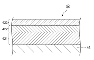
- FIG. 6 shows a light selective absorption film including a base material, an infrared reflection layer, a sunlight absorption layer, and an antireflection layer as a cross-sectional view of one embodiment of the light selective absorption film.
- the light selective absorption film 42 has an infrared reflection layer 421, an absorption layer 422, and an antireflection layer 423 in this order from the heat collecting tube main body 41, and has a high solar energy absorption rate ⁇ and 450 ° C. or less in a wavelength region of 300 to 2500 nm. Can achieve both low emissivity ⁇ . Therefore, when a heat collecting tube having this light selective absorption film is used as a heat collecting tube for solar power generation, the power generation efficiency of the solar power generation device can be effectively improved.
- the solar energy absorption rate ⁇ is weighted by multiplying the measured values of spectral reflectance and transmittance of 300 to 2500 nm by the weight coefficient indicating the spectral distribution of standard solar radiation in accordance with ISO 9050-2003. It is defined by a value obtained by subtracting the solar energy reflectance and solar energy transmittance calculated by averaging from 100%, and ⁇ is represented by the following formula (1).
- ⁇ (%) 100 (%) ⁇ (solar energy reflectance, unit:%) ⁇ (solar energy transmittance, unit:%) (1)
- the emissivity ⁇ is a ratio of black body radiation having the same temperature as an object when an object having a certain temperature emits thermal radiation.
- ⁇ is the value of the ratio at 450 ° C. or less, which is the operating temperature of solar thermal power generation, and is a value measured in a wavelength range of 2 to 22 ⁇ m.
- the light selective absorption film 42 of the present invention can have an average reflectance in the wavelength range of 300 to 2500 nm of less than 10%, more preferably less than 5%. Further, the average reflectance in the wavelength range of 2 to 22 ⁇ m can be 80% or more. More preferably, it can be 90% or more. Further, such a light selective absorption film 42 has a solar energy absorption rate ⁇ of 90% or more, more preferably ⁇ can be 95% or more. The emissivity ⁇ can be less than 20%, more preferably ⁇ can be less than 10%.
- the light selective absorption film of the present invention is formed easily and stably compared to, for example, a structure having a cermet layer or a structure having a large number of layers because the constituent material of each layer is simple. it can.
- the absorption layer 422 has a function of absorbing light in the visible region and near infrared region and reflecting or transmitting light in the infrared region to improve the wavelength selectivity of the light selective absorption film.
- the absorption layer 422 is made of a metal nitride containing at least one metal element selected from the group consisting of Cr, Fe and Ni, Si and N.
- the absorption layer 422 may be a single layer or multiple layers as long as it exhibits the above function.
- the total content of the specific metal element, silicon and nitrogen in the metal nitride is 70 atomic% or more. That is, the content of other elements is allowed at 30 atomic% or less. From the viewpoint of increasing the absorption rate of the absorption layer, the content of the entire absorption layer is preferably 90 atomic percent or more, and the content of other elements is allowed to be 10 atomic percent or less. Examples of the other element include oxygen (O).
- the atomic composition percentage (atomic%) of the component is a value obtained by dividing the peak area measured by X-ray photoelectron spectroscopy (XPS) by the sensitivity factor of each element (corresponding to the number of atoms of each element). To calculate). Similarly, the atomic ratio of the content of each element is also measured and calculated by XPS.
- XPS X-ray photoelectron spectroscopy
- the content of Si with respect to the total amount of Cr, Fe and Ni (Cr + Fe + Ni) satisfies the relationship of the following formula (2) in terms of atomic ratio. 0.7 ⁇ Si / (Cr + Fe + Ni) ⁇ 2 (2)
- the lower limit of the formula (2) is more preferably 0.9, and even more preferably 1.1.
- the upper limit of the formula (2) is more preferably 1.8, and further preferably 1.5.
- the content of N with respect to the total amount of Cr, Fe and Ni satisfies the relationship of the following formula (3) in terms of atomic ratio. 0.9 ⁇ N / (Cr + Fe + Ni) ⁇ 2.2 (3)
- the lower limit of formula (3) is more preferably 1.1, and still more preferably 1.3.
- the upper limit of the formula (3) is more preferably 2.0, and even more preferably 1.7.
- the metal element in the metal nitride is preferably composed of at least one of Fe and Ni from the viewpoint of increasing the absorption rate of the absorption layer and improving heat resistance. And it is more preferable that it consists of both elements of Fe and Ni.
- the metal nitride is preferably represented by a chemical composition M 1 Si x N y (M 1 is at least one metal selected from the group consisting of Cr, Fe and Ni).
- the absorption layer is more preferably made of M 1 Si x N y excluding inevitable impurities.
- x is the relative number of atoms of Si to 1 atom of M 1
- y represents the relative number of atoms of N for 1 atom of M 1. Both x and y are not 0, and as described above, x is preferably 0.7 to 2, and y is preferably 0.9 to 2.2.
- M 1 is preferably at least one of Fe and Ni, and M 1 more preferably contains both Fe and Ni.
- the metal nitride may be crystalline or amorphous.
- the metal-silicon nitride in atomic percent composition, the M 1 15 ⁇ 35%, the Si 25 ⁇ 45%, preferably contains N 20 ⁇ 60%.
- M 1 is both Fe and Ni
- the Fe content is more preferably 15 to 30 atomic%, particularly preferably 20 to 25 atomic%, based on the entire metal nitride.
- the physical layer thickness of the absorption layer 422 (hereinafter also referred to as layer thickness) is preferably 30 to 150 nm. When the layer thickness of the absorption layer 422 is within the above range, the wavelength selectivity by the absorption layer 422 can be effectively improved.
- the layer thickness of the absorption layer 422 is more preferably 50 to 120 nm, and more preferably 80 to 110 nm. In the present specification, the layer thickness refers to a value calculated by the following formula (4) from the deposition rate and deposition time of each layer.
- the light selective absorption film of the present invention may have a layer having a wavelength selection characteristic similar to that of the absorption layer and made of a material different from the absorption layer (hereinafter referred to as an absorption auxiliary layer).
- the absorption auxiliary layer is preferably in contact with the absorption layer, and more preferably between the absorption layer and the infrared reflection layer.
- the absorption efficiency of the absorption auxiliary layer in the wavelength range of 300 to 2500 nm is generally lower than that of the absorption layer. However, when the absorption auxiliary layer is provided adjacent to the absorption layer, the absorption efficiency of the entire light selective absorption film can be increased.
- the absorption auxiliary layer is preferably made of a metal silicide having the same wavelength selectivity as the absorption layer.
- This metal silicide may contain a nonmetallic element, but when it contains nitrogen atoms, it is preferable that the content of nitrogen is lower than that of the metal nitride of the absorption layer and substantially no nitrogen atoms are contained. Moreover, it is a different substance from the material of the infrared reflective layer mentioned later.
- the absorption assisting layer is preferably made of a metal silicide containing Fe and Si and not containing nitrogen. Examples of the metal other than Fe contained in the metal silicide include Cr and Ni.
- the metal silicide preferably contains at least one of Cr or Ni, Fe and Si.
- the total content of these elements is preferably 70 atomic% or more, more preferably 90 atomic% or more in the metal silicide.
- the content of Si with respect to the total amount of Cr, Fe and Ni is expressed by an atomic ratio, and the relationship of the following formula (5) satisfies the following relationship.
- the lower limit value of the formula (5) is more preferably 0.7, and further preferably 0.9.
- the upper limit of formula (5) is more preferably 1.3, and even more preferably 1.1.
- the metal element of the absorption auxiliary layer preferably contains both elements of Fe and Ni from the viewpoint of increasing the absorption rate of the absorption layer and improving heat resistance.
- the absorption auxiliary layer has a chemical composition, and the content of a compound represented by M 1 Si z (M 1 is at least one of Cr or Ni and Fe) is 70 atomic% or more, preferably 90 atomic%. That's it.
- the absorption auxiliary layer is more preferably composed of the above compound except for inevitable impurities.
- z represents the relative number of atoms of Si with respect to one atom of M 1 . As described above, z is preferably 0.5 to 1.5.
- M 2 Si x (M 2 is Fe and Ni) preferably contains a compound represented by the chemical composition of.
- the Fe content is more preferably from 15 to 30 atomic%, particularly preferably from 20 to 25 atomic%, based on the entire compound of the absorption assisting layer.
- the physical layer thickness of the absorption auxiliary layer is preferably 1 to 50 nm. When the thickness of the absorption assisting layer is within the above range, the wavelength selection characteristic of the absorption assisting layer can be effectively improved. Further, the layer thickness of the absorption assisting layer is more preferably 3 to 40 nm, and more preferably 5 to 30 nm.
- the infrared reflection layer 421 absorbs visible light and near infrared light of sunlight, and reflects infrared light emitted from the heat medium. Thereby, the emissivity of the light selective absorption film can be lowered.
- the infrared reflective layer 421 may be a single layer or multiple layers as long as it exhibits the above function.
- the composition of the infrared reflection layer 421 is not limited as long as it functions as described above.
- the infrared reflective layer is preferably composed of one or more selected from the following metal element group. That is, selected from the group consisting of Ag, Al, Au, Cu, Cr, Hf, La, Mo, Ni, Pd, Pt, Rh, Si, Ta, Ti, Zr and W (hereinafter referred to as the first element group). It is preferable that it consists of 1 or more types of the element made. As described above, the first element group does not contain Fe.
- the material of the infrared reflective layer is a single metal selected from the metal elements of the first element group, or an intermetallic compound, alloy, solid solution, etc. composed of two or more selected from the metal elements of the first element group. Preferably there is. In particular, a simple metal or an intermetallic compound is preferable. However, inevitable impurities are allowed to be mixed.
- the infrared reflection layer is preferably Mo alone or nickel silicide in order to reflect infrared light and lower the emissivity of the light selective absorption film. From the viewpoint of enhancing reflection of light in the infrared region, nickel silicide is more preferable.
- the nickel silicide preferably satisfies the relationship expressed by the following formula (6) in terms of the content of Si with respect to Ni as an atomic ratio. 0.7 ⁇ Si / Ni ⁇ 1.5 (6) From the viewpoint of improving the photoselectivity of the infrared reflecting layer, the lower limit of Si / Ni is more preferably 0.9, and the upper limit is more preferably 1.3.
- the infrared reflective layer 421 is a multilayer, for example, a layer made of either Mo or nickel silicide described above (hereinafter referred to as a first layer) and a layer mainly composed of Ag alone or an alloy containing Ag ( Hereinafter, a combination having a second layer) may be mentioned.
- the first layer is preferably a layer made of nickel silicide as described above.
- the second layer is preferably a layer made of Ag alone.
- the second layer is between the first layer and the absorbing layer.
- the thickness of the physical layer of the entire infrared reflection layer 421 is preferably 50 to 1000 nm.
- the thickness of each layer may be the same or different.
- the layer thickness of the entire infrared reflection layer 421 is within the above range, sufficient wavelength selectivity can be obtained.
- the layer thickness of the infrared reflecting layer 421 that is first laminated on the heat tube main body 41 is more preferably 150 to 700 nm, and more preferably 200 to 600 nm.
- a base layer not shown in FIG. 6 may be provided between the infrared reflective layer 421 and the base material from the viewpoint of improving heat resistance. Thereby, the heat resistance of the light selective absorption film can be improved without affecting the optical characteristics.
- the underlayer is made of, for example, an element selected from the group consisting of Al, Ce, Hf, In, La, Nb, Sb, Si, Sn, Ta, Ti, Zn, and Zr (hereinafter referred to as a second element group).
- An oxide or a composite oxide containing one or more elements selected from these elements is preferable.
- an oxide of Si or Ge, or a composite oxide containing one or more elements selected from Si and Ge is preferable.
- a composite oxide containing silicon oxide (chemical formula SiO w , where w is 2 or less) or Si is more preferable, and an oxide of Si is more preferable.
- the physical layer thickness of the entire underlayer is preferably 100 to 500 nm from the viewpoint of improving heat resistance.
- the layer thicknesses of the underlayers may be the same or different from each other, but are preferably within the above range as a whole.
- the layer thickness of the underlayer is more preferably 150 to 400 nm, further preferably 200 to 350 nm.
- the antireflection layer 423 prevents reflection of light in the visible region and near infrared region. This layer can increase the absorption rate of the light selective absorption film.
- the antireflection layer 423 is not particularly limited as long as it has excellent heat resistance and chemical stability, and can provide a good antireflection function in the visible region and near infrared region due to optical interference as a low refractive index substance.
- the antireflection layer 423 is a layer having a refractive index at a wavelength of 550 nm of 1.9 or less and an extinction coefficient representing light absorption by a substance of 0.01 or less from the viewpoint of increasing the absorption rate of the light selective absorption film. ,preferable.
- the antireflection layer 423 is preferably made of a dielectric material having the above optical characteristics.
- a dielectric material of the antireflection layer an oxide, oxynitride and nitride of an element selected from the second element group, or a composite containing one or more elements selected from the second element group Those selected from oxides, complex oxynitrides and complex nitrides are preferred.
- silicon oxide (chemical formula SiO t , t is represented by 2 or less) or Al oxide (represented by chemical formula Al 2 O 3 ), or one or more elements selected from Si and Al
- a composite oxide containing is preferable.
- a composite oxide containing silicon oxide or Si is more preferable, and silicon oxide is more preferable.
- Silicon oxide is excellent in heat resistance and chemical stability, and as a low refractive index substance, a good antireflection function can be obtained in the visible range by optical interference.
- the thickness of the physical layer of the antireflection layer 423 is preferably 40 to 150 nm from the viewpoint of effectively obtaining the above functions.
- the thickness of the antireflection layer 423 is more preferably 50 to 130 nm, and further preferably 60 to 110 nm.
- Such a light selective absorption film 42 can be suitably formed by a dry method such as a sputtering method, an electron beam evaporation method, or a vacuum evaporation method.
- a dry method such as a sputtering method, an electron beam evaporation method, or a vacuum evaporation method.
- the sputtering method is preferable from the viewpoint of improving the productivity because the deviation of the film thickness distribution is small.
- an alternating current (AC) or direct current (DC) sputtering method can be used as the sputtering method.
- the DC sputtering method includes a pulse DC sputtering method.
- AC sputtering or pulse DC sputtering is effective in preventing abnormal discharge.
- AC or DC reactive sputtering is effective in that a dense film can be formed.
- an infrared reflective layer is formed on a stainless steel substrate as a sputtering method.
- a target used for forming the infrared reflective layer for example, a target made of a single metal consisting of the first element group or a compound containing one or more elements selected from the first element group is used.
- a nickel silicide target or a molybdenum (Mo) target is more preferable from the viewpoints of heat resistance of the metal layer to be formed, chemical stability, adhesion to the heat collecting tube main body 41 serving as a base material, and the like.
- a layer is formed by performing sputtering in argon gas atmosphere, for example.
- an absorption layer 422 is formed on the infrared reflection layer 421 by a sputtering method.
- a target having at least one metal element selected from the group consisting of Cr, Fe and Ni and silicon is used.
- a layer is formed by performing sputtering in the atmosphere containing argon gas and nitrogen gas, for example.
- the absorption layer 422 preferably contains Ni, Fe, Si, and N as described above.
- the layer can be formed by performing sputtering in an atmosphere containing nitrogen gas using a target made of an alloy made of Si, Ni and Fe or an intermetallic compound.
- the absorbing layer can be formed by co-sputtering two or three kinds of targets in an atmosphere containing nitrogen gas.
- three types of targets three types of targets are used: a Si target, a Ni target, and a Fe target.
- a combination of a Si target and a Ni—Fe alloy target, a Ni target and a Fe—Si alloy or a Fe—Si intermetallic compound target, or a Fe target and a Ni—Si alloy or A combination with a Ni—Si intermetallic compound target is used.
- the one target described here may be a chip of a type mounted on the other target, or may be a plurality of independent targets directly connected to different power sources.
- an antireflection layer 423 is formed on the absorption layer 422.
- a layer is formed by performing sputtering in an oxidizing atmosphere containing, for example, argon gas and oxygen gas using a metal Si target.
- the obtained light selective absorption film 42 was placed in a vacuum firing furnace, the inside of the vacuum chamber was evacuated to, for example, 8 Pa, the furnace temperature was raised to 450 ° C., held for 30 minutes, and then lowered to 100 ° C. Later, it is taken out from the vacuum firing furnace. By heating in vacuum, crystallization of the film is promoted, a solar energy absorption rate ⁇ is high, and a light selective absorption film having a low emissivity ⁇ at 450 ° C. or less is obtained.
- a metal or glass typically stainless steel
- metals other than stainless steel include Cu, Mo, Ni, and alloys containing one of these.
- Stainless steel or glass is preferred for solar collector applications.
- stainless steel is more preferable from the viewpoint of the strength of the substrate and the reliability with respect to heat.
- a base material is used properly also according to adhesiveness with an infrared reflective layer.
- stainless steel is preferable when Mo is used as the infrared reflecting layer.
- glass is preferred when nickel silicide is used.
- FIG. 2 is a plan view showing an embodiment of the heat collecting tube 4 used in the parabolic trough heat collector 1.
- 3 is a cross-sectional view of the heat collecting tube 4 shown in FIG.
- the heat collection tube 4 has a heat collection tube main body 41 made of a stainless steel tube or the like through which a heat medium flows, and a light selective absorption film 42 is provided on the outer surface thereof.
- a glass tube 43 is provided outside the heat collecting tube main body 41 at a predetermined interval so as to cover the heat collecting tube main body 41. Both ends of the heat collecting tube main body 41 and the glass tube 43 are fixed by the fixing brackets 44 so that a vacuum state is established therebetween.
- the heat collecting tube of the present invention is characterized in that the light selective absorption film 42 provided on the outer surface of the heat collecting main body 41 is the above-described light selective absorption film of the present invention.
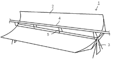
- FIG. 1 is an external view of a parabolic trough heat collector as an embodiment of a heat collector in a solar thermal power generation apparatus.
- the parabolic trough heat collector 1 has a parabolic reflector 2 that is a parabolic reflector as a condensing means.
- the parabolic reflector 2 is supported by a reflector support 3.
- a heat collecting tube 4 is provided at the focal portion of the parabolic reflector 2 so as to extend along the focal portion.
- the heat collecting tube 4 is fixed to the parabolic reflecting mirror 2 and the reflecting mirror support 3 by a heat collecting tube support 5.
- parabolic trough heat collector 1 In such a parabolic trough heat collector 1, sunlight is condensed on the heat collecting tube 4 by the parabolic reflecting mirror 2, and the heat collecting tube 4 is heated by the condensed sunlight. A heat medium such as oil flows inside the heat collecting tube 4, and the heat medium inside the heat collecting tube 4 is heated by heating the heat collecting tube 4.
- the parabolic trough heat collector 1 is connected to a steam turbine, and power is generated by rotating the steam turbine using the heat of the heat medium.
- FIG. 4 is an external view of a linear Fresnel type heat collector as another embodiment of the heat collector in the solar thermal power generation apparatus.
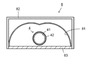
- FIG. 5 is sectional drawing which shows the receiver of the linear Fresnel type heat collector shown in FIG.
- the linear Fresnel type heat collector 6 has, for example, a plurality of parallel plate-like first reflecting mirrors 7 serving as light collecting means, and a position between them in parallel with and higher than these.
- the receiver 8 is disposed in The receiver 8 is fixed by, for example, a receiver support 9.
- the receiver 8 houses the heat collecting tube 4, a second reflecting mirror 81 as a condensing means for collecting the reflected light of the first reflecting mirror 7 on the heat collecting tube 4, and the second reflecting mirror 81.
- 1 has a case portion 82 having an opening on the reflecting mirror 7 side and a glass plate 83 disposed in the opening portion of the case portion 82.
- the heat collecting tube 4 of the linear Fresnel type heat collector 6 has, for example, a heat collecting tube main body 41 made of a stainless steel tube or the like in which a heat medium flows, and a light selective absorption film 42 is provided on the outer surface thereof.
- the solar thermal power generation device is not necessarily limited to the one using a parabolic trough type heat collector or a linear Fresnel type heat collector.
- the light selective absorption film is applied, another type of solar thermal power generation apparatus may be used.
- the light selective absorption film those used for the heat collecting tube of the solar thermal power generation device can be cited as typical ones.
- the light selective absorption film is not necessarily limited to the heat collecting tube of the solar thermal power generation device, and is used in applications where similar functions are required. If it exists, it may be used for other purposes.
- Examples 1 to 6 are examples of the present invention, and Example 7 is a comparative example.
- Table 1 shows the base materials, film configurations, and physical layer thicknesses of Examples 1 to 7.
- Example 1 A glass substrate having a length of 50 mm, a width of 50 mm, and a thickness of 2 mm was used as a substrate, and a light selective absorption film 42 having a laminated structure was formed on the glass substrate by a sputtering method.
- Targets 1 to 3 the following three types of targets (targets 1 to 3), all having a size of 15.2 cm (6 inches) ⁇ were used.
- Targets 1 to 3 the following three types of targets (targets 1 to 3), all having a size of 15.2 cm (6 inches) ⁇ were used.
- a cleaned glass substrate was placed in the vacuum layer, and targets 1 to 3 were placed facing the glass substrate above the cathode, respectively. Then, the inside of the vacuum chamber was evacuated to 2 ⁇ 10 ⁇ 3 Pa, and the following film formation was performed.
- Step 1 Formation of infrared reflection layer
- a nickel silicide film (NiSi film) was formed on a glass substrate by DC pulse sputtering.
- Argon gas was introduced as a sputtering gas at 8.3 ⁇ 10 ⁇ 4 L / s.
- the input power was 300 W and the pulse frequency was 20 kHz.
- the thickness of the obtained nickel silicide film was 400 nm.
- the atomic ratio (Si / Ni) of nickel silicide was 1.
- Step 2 Formation of absorption layer
- a metal nitride film containing Ni, Fe and Si ((Ni a Fe 1-a ) Si x N y film) is formed on a glass substrate having a nickel silicide film by DC pulse sputtering using the target 2.
- As sputtering gas argon gas was introduced at 4.2 ⁇ 10 ⁇ 4 L / s and nitrogen gas was introduced at 4.2 ⁇ 10 ⁇ 4 L / s.
- the input power was 300 W and the pulse frequency was 20 kHz.
- the obtained metal nitride film had a thickness of 90 nm.
- Step 3 Formation of antireflection layer
- SiO 2 film SiO 2 film
- argon gas was introduced at 4.2 ⁇ 10 ⁇ 4 L / s
- oxygen gas was introduced at 4.2 ⁇ 10 ⁇ 4 L / s.
- the input power was 300 W and the pulse frequency was 20 kHz.
- the thickness of the obtained silicon oxide film was 90 nm.
- Example 2 A sample of the selective absorption film according to Example 2 was produced in the same manner as in Example 1.
- Example 2 a stainless steel (JIS standard SUS304) substrate 50 mm long ⁇ 50 mm wide ⁇ 1 mm thick whose surface was polished so that the arithmetic average surface roughness Ra was about 0.2 ⁇ m was used.
- Other conditions are the same as in Example 1.
- Example 3 A sample of the selective absorption membrane according to Example 3 was prepared in the same manner as in Example 1. In Example 3, the following processing was performed between Step 1 and Step 2.
- a metal silicide film ((Ni c Fe 1-c ) Si z film) containing Ni, Fe and Si was formed by DC pulse sputtering.
- Argon gas was introduced as a sputtering gas at 8.3 ⁇ 10 ⁇ 4 L / s.
- the input power was 300 W and the pulse frequency was 20 kHz.
- the obtained metal silicide film had a thickness of 25 nm.
- Example 4 A sample of the selective absorption film according to Example 4 was produced in the same manner as in Example 3. In Example 4, the same substrate as in Example 2 was used. Other conditions are the same as in Example 3.
- Example 5 A sample of the selective absorption film according to Example 5 was produced in the same manner as in Example 1.
- a molybdenum film (Mo film) was formed by DC pulse sputtering using a molybdenum target instead of a nickel silicide target.
- Argon gas was introduced into the sputtering gas at 8.3 ⁇ 10 ⁇ 4 L / s.
- the input power was 300 W and the pulse frequency was 20 kHz.
- the obtained molybdenum film had a thickness of 400 nm.
- Other conditions are the same as in Example 1.
- Example 6 A sample of the selective absorption film according to Example 6 was produced in the same manner as in Example 5. In Example 6, the same substrate as in Example 2 was used. Other conditions are the same as in Example 5.
- Example 7 A cleaned glass substrate having a length of 50 mm, a width of 50 mm, and a thickness of 2 mm was placed in the vacuum layer. A selective absorption film having a laminated structure was formed on this glass substrate by sputtering.
- Example 7 the following two types of targets (targets 4 and 5) were both used with a size of 15.2 cm (6 inches) ⁇ .
- a cleaned glass substrate was placed in the vacuum layer, and targets 4 and 5 were placed facing the glass substrate above the cathode, respectively. Then, the inside of the vacuum chamber was evacuated to 2 ⁇ 10 ⁇ 3 Pa, and the following film formation was performed.
- Step 1 Formation of infrared reflection layer
- a nickel titanium film (NiTi x film) was formed on a glass substrate by a DC pulse sputtering method.
- Argon gas was introduced as a sputtering gas at 8.3 ⁇ 10 ⁇ 4 L / s.
- the input power was 300 W and the pulse frequency was 20 kHz.
- the thickness of the obtained nickel titanium film was 50 nm.
- Step 2 Formation of absorption layer
- a DC pulse sputtering on a glass substrate having a nickel-titanium film was deposited nickel titanium nitride film (NiTi v N w film).
- argon gas was introduced at 4.2 ⁇ 10 ⁇ 4 L / s and nitrogen gas was introduced at 4.2 ⁇ 10 ⁇ 4 L / s.
- the input power was 300 W and the pulse frequency was 20 kHz.
- the thickness of the obtained nickel titanium nitride film was 100 nm.
- Step 3 Formation of antireflection layer
- a silicon oxide film was formed on the nickel titanium nitride film by DC pulse sputtering.
- sputtering gas argon gas was introduced at 4.2 ⁇ 10 ⁇ 4 L / s, and oxygen gas was introduced at 4.2 ⁇ 10 ⁇ 4 L / s.
- the input power was 300 W and the pulse frequency was 20 kHz.
- the thickness of the obtained silicon oxide film was 100 nm.
- a selective absorption film sample in which two layers were laminated on a glass substrate was obtained.
- This sample was placed in a vacuum firing furnace, the inside of the vacuum chamber was evacuated to 8 Pa, the temperature in the furnace was raised to 450 ° C., held for 30 minutes, then cooled to 100 ° C. and then taken out from the vacuum firing furnace for evaluation. It was.
- the chemical composition in Table 2 is the chemical composition expressed as a percentage of the atomic composition of the absorption layers in Examples 1 to 6.
- the atomic ratio is the atomic ratio of Si to the total amount of Cr, Fe and Ni (Si / (Cr + Fe + Ni)) and the atomic ratio of N to the total amount of Cr, Fe and Ni (N / (Cr + Fe + Ni)). It is.
- Table 3 shows the chemical composition of the absorption auxiliary layers of Examples 3 and 4.
- the atomic ratio is the atomic ratio of Si to the total amount of Ni, Fe and Cr (Si / (Cr + Fe + Ni)).
- Table 4 shows the chemical compositions of the infrared reflective layers of Examples 1 to 4.
- the atomic ratio represents the atomic ratio between Si and Ni.
- Table 5 shows the solar energy absorption rate ⁇ and emissivity ⁇ of Examples 1 to 7.
- the absorptance ⁇ is a value obtained by subtracting solar energy reflectance and solar energy transmittance from 100%.
- the solar energy reflectance and solar energy transmittance are values obtained by multiplying the measured values of the spectral reflectance and spectral transmittance of 300 to 2500 nm by the weight coefficient indicating the standard spectral distribution of solar radiation in accordance with ISO 9050-2003. Was calculated.
- Spectral reflectance and spectral transmittance were measured using a spectrophotometer (trade name: U4100, manufactured by HITACHI).
- the emissivity ⁇ was determined using an emissivity measuring instrument (manufactured by Japan Sensor Co., Ltd., trade name: TSS-5X) in the wavelength range of 2 to 22 ⁇ m.
- the silicon oxide (SiO 2 ) films produced under the conditions of Examples 1 to 7 had a refractive index of 1.472 at a wavelength of 550 nm and an extinction coefficient of 0.00.
- the refractive index and extinction coefficient were analyzed using a spectroscopic ellipsometer (manufactured by JA Woollam Japan, trade name: M-2000DI).
- Table 1 shows the base material, film configuration and layer thickness of the evaluation substrate.
- Table 2 shows the chemical composition of the absorption layer of the evaluation substrate.
- Table 3 shows the chemical composition of the absorption auxiliary layer of the evaluation substrate.
- Table 4 shows the chemical composition of the infrared reflective layer of the evaluation substrate.
- Table 5 shows the absorption rate ⁇ and emissivity ⁇ of the evaluation substrate.
- Examples 1, 3, and 5 are examples in which a light selective absorption film is formed on a glass substrate.
- the absorptance ⁇ is 90% or more and the emissivity ⁇ is 11% or less. It shows that it has a low reflectance in the wavelength range of the sunlight spectrum and has a high reflectance in the wavelength range of the infrared spectrum.
- Examples 2, 4, and 6 are examples in which a light selective absorption film is formed on a stainless steel substrate.
- the absorption rate is 95% or higher, which is higher than the film on the glass substrate.
- the emissivity ⁇ was 20% or less, and in Example 6, a low emissivity of 10% was realized.
- Example 7 is an example in which a light selective absorption film is formed on a glass substrate, and the absorptance ⁇ is 61.8% and the emissivity ⁇ is 16%. Compared with Example 1, Example 3, and Example 5, the absorptance is low and the emissivity is high, so it can be said that the film is inferior in photoselectivity.
- the film-coated substrate of Example 6 was held in a vacuum at 550 ° C. for 600 hours. After holding, the absorption rate ⁇ was 96.0%, and the emissivity ⁇ was 9.0%. Absorptivity ⁇ was improved and emissivity ⁇ was not changed. From this, it can be said that the selective absorption film of the present invention has high heat resistance without deterioration of the characteristics even at a high temperature of 550 ° C. in vacuum.
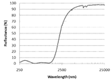
- FIG. 7 shows the spectral reflectance from a wavelength of 250 to 25000 nm after holding Example 6 in a vacuum at 550 ° C. for 600 hours.
- the reflectance at a wavelength of 5 ⁇ m is 92.7%, which is 90% or more, which indicates that it has a low emissivity in the operating temperature range near 400 ° C.
- the above-mentioned spectrophotometer (manufactured by HITACHI, trade name: U4100) is used for the wavelength range of 250 to 2500 nm, and the Fourier transform infrared spectroscopy (FT-IR) is used for the wavelength range of 2500 to 25000 nm. ) Measuring instruments (manufactured by Thermo Fisher Scientific, trade name: NICOLET6700) were used. It should be noted that the entire content of the specification, claims, abstract and drawings of Japanese Patent Application No. 2012-149859 filed on July 3, 2012 is cited here as the disclosure of the specification of the present invention. Incorporated.
- SYMBOLS 1 DESCRIPTION OF SYMBOLS 1 ... Parabolic trough type collector, 2 ... Parabolic reflector, 3 ... Reflector support body, 4 ... Heat collecting tube, 6 ... Linear Fresnel type collector, 7 ... First reflector, 8 ... Receiver, 9 DESCRIPTION OF SYMBOLS ... Receiver for receiver, 41 ... Heat collecting tube main body, 42 ... Light selective absorption film, 43 ... Glass tube, 44 ... Fixing bracket, 81 ... Second reflector, 82 ... Case part, 83 ... Glass plate, 421 ... Infrared ray Reflective layer, 422 ... absorbing layer, 423 ... antireflection layer
Landscapes
- Engineering & Computer Science (AREA)
- Physics & Mathematics (AREA)
- Chemical & Material Sciences (AREA)
- Sustainable Development (AREA)
- Sustainable Energy (AREA)
- Thermal Sciences (AREA)
- Life Sciences & Earth Sciences (AREA)
- Combustion & Propulsion (AREA)
- Mechanical Engineering (AREA)
- General Engineering & Computer Science (AREA)
- Spectroscopy & Molecular Physics (AREA)
- Surface Treatment Of Glass (AREA)
- Physical Vapour Deposition (AREA)
Abstract
ISO9050-2003に準じた300~2500nmの日射エネルギー吸収率αが高く、使用温度である450℃以下での放射率εが低くなる波長選択性を有し、膜構成が簡単で生産性の高い光選択吸収膜の提供。 基材上に形成される光選択吸収膜であって、前記基材側から順に赤外線反射層、太陽光の吸収層および反射防止層をこの順番に有し、前記吸収層が、Cr、FeおよびNiからなる群より選択される少なくとも1種の金属元素、ケイ素および窒素を70原子%以上で含有する金属窒化物からなることを特徴とする光選択吸収膜。
Description
本発明は、光選択吸収膜、集熱管および太陽熱発電装置に係り、特に太陽熱発電装置用の集熱管の表面に好適に形成される光選択吸収膜、該光選択吸収膜を有する集熱管および太陽熱発電装置に関する。
太陽熱発電は、例えば、鏡等の太陽光反射板により太陽光を集光して熱を発生させ、この熱によりオイル等の熱媒体を加熱し、この熱を蒸気に変換し、蒸気タービンを回転させて発電を行う発電方式である。発電の原理は伝統的な火力発電と基本的に同様であるが、熱の発生に燃料の燃焼ではなく、太陽熱を利用する点で環境に優しい発電方式である。
太陽熱発電には、パラボリックトラフ式、リニアフレネル式、ディッシュ式、タワー式等の方式がある。例えば、パラボリックトラフ式は、太陽光反射板となる雨樋形状の曲面鏡と、この曲面鏡の焦点付近に沿って設置されたパイプ状の集熱管とを有し、太陽光を曲面鏡によって集熱管に集光し、この集熱管内を流れるオイル等の熱媒体を加熱し、これにより発電する発電方式である。タワー式太陽熱発電と比較すると、太陽光反射板の配置が容易なことから大規模な施設の建設が容易である点で優れる。
集熱管には、太陽熱で熱媒体を効率よく加熱し、また加熱された熱媒体の熱損失防止を目的として、光選択吸収膜が設けられる。そのため、光選択吸収膜は、日射エネルギーを効率よく吸収し、かつ、集熱管から外部への熱放射を低減する特性が求められている。
従来、前記光選択吸収膜として、TiSi層、TiO2層およびSiO2層を有するものが提案されていた(特許文献1参照)。しかし、このような光選択吸収膜では層数が多くなりやすく、構成が複雑となり、また各層の厚さを精密に制御する必要があり、大量生産に適していなかった。
また、特許文献2には、光選択吸収膜として、誘電体層と、クロム、窒化クロムおよび酸窒化クロムからなる群より選択された1種以上のクロム系層とを有するものが提案されている。しかし、このような光選択吸収膜は主として太陽熱温水器に用いられるものであり、太陽熱発電における集熱管の作動温度である400℃付近に相当する波長4~5μmの波長域の放射率は必ずしも低くない。すなわち、上記波長域の反射率は必ずしも十分に高くなく、太陽熱発電の集熱管に適用した場合、集熱管から外部への熱放射が高くなるおそれがある。
特許文献3には、光選択吸収膜として、MoとSiO2のサーメット層を有するものが提案されている。しかし、サーメット層は、金属相と酸化物などのセラミックス相が共存した層であり、スパッタリング法のような、一旦原子状に分解した材料を再形成して薄膜を製造するような方法では、金属相と酸化物が共存する状態を安定的に形成することは容易でなく、サーメット層の形成には、高周波(RF)スパッタリング法や反応性共スパッタリング法(リアクティブ・コスパッタリング法)などを用いる必要があるが、これらの成膜方法は、生産性が低いといった問題があった。
本発明は、上記課題を解決するためになされたものであって、ISO9050-2003に準じた300~2500nmの日射エネルギー吸収率αが高く、使用温度である450℃以下での放射率εが低くなる波長選択性を有し、膜構成が簡単で生産性の高い光選択吸収膜の提供を目的とする。また、本発明は、このような光選択吸収膜を有する集熱管および太陽熱発電装置の提供を目的とする。
本発明の光選択吸収膜は、基材上に形成される光選択吸収膜であって、前記基材側から順に赤外線反射層、太陽光の吸収層および反射防止層をこの順番に有し、前記吸収層が、Cr、FeおよびNiからなる群より選択される少なくとも1種の金属元素、ケイ素および窒素を含有する金属窒化物からなり、前記金属窒化物における前記特定の金属元素、ケイ素および窒素の合計の含有量が70原子%以上であることを特徴とする。
本発明の集熱管は、外面に光選択吸収膜を有する集熱管本体と、前記集熱管本体の外側を囲むようにして設けられたガラス管とを有する集熱管であって、上記した本発明の光選択吸収膜が本発明の光選択吸収膜であることを特徴とする。
本発明の太陽熱発電装置は、集熱管と、前記集熱管に太陽光を集光する集光手段とを有する集熱器を備える太陽熱発電装置であって、前記集熱管が上記した本発明の集熱管であることを特徴とする。
本発明によると、300~2500nmの波長域において高い日射エネルギー吸収率αと、450℃以下において低い放射率εとを同時に達成し、さらに耐熱性の良好な光選択吸収膜を提供できる。また、膜構成が簡単であり、生産性に優れる。さらに、本発明の集熱管および太陽熱発電装置は、このような光選択吸収膜を有するため太陽熱発電の発電効率を向上できる。
以下、本発明の実施の形態について説明する。本明細書において、元素記号(例えば、「Cr」)は元素を示し、特に言及しない限り、その元素単体の物質(例えば、金属)を示すものではない。
(光選択吸収膜)
本発明の光選択吸収膜は、基材側から順に、赤外線反射層、太陽光の吸収層および反射防止層を有する。なお、上記3つの層をこの順で有する限り、各層の間、赤外線反射層と基材との間および反射防止層の上側に他の層を有してもよい。生産性向上の観点から、光選択吸収膜は、赤外線反射層、太陽光の吸収層および反射防止層からなることが好ましい。なお、以下「太陽光の吸収層」を単に「吸収層」ともいう。
本発明の光選択吸収膜は、基材側から順に、赤外線反射層、太陽光の吸収層および反射防止層を有する。なお、上記3つの層をこの順で有する限り、各層の間、赤外線反射層と基材との間および反射防止層の上側に他の層を有してもよい。生産性向上の観点から、光選択吸収膜は、赤外線反射層、太陽光の吸収層および反射防止層からなることが好ましい。なお、以下「太陽光の吸収層」を単に「吸収層」ともいう。
前記赤外線反射層は、熱媒体から放射される赤外スペクトル域の光を反射する役割を有する。これにより、光選択吸収膜が、低放射特性を示す。
前記吸収層は、太陽光スペクトル域の光を吸収する役割を有する。本発明において、吸収層は、Cr、FeおよびNiからなる群より選ばれる少なくとも1種の金属元素、SiおよびNを主成分とする金属窒化物からなる。
前記反射防止層は、太陽光スペクトル域の光の反射を抑制する役割を有する。これにより、前記吸収層への太陽光の入射を高められる。
前記吸収層は、太陽光スペクトル域の光を吸収する役割を有する。本発明において、吸収層は、Cr、FeおよびNiからなる群より選ばれる少なくとも1種の金属元素、SiおよびNを主成分とする金属窒化物からなる。
前記反射防止層は、太陽光スペクトル域の光の反射を抑制する役割を有する。これにより、前記吸収層への太陽光の入射を高められる。
図6に、光選択吸収膜の一実施形態の断面図として、基材、赤外線反射層、太陽光の吸収層および反射防止層からなる光選択吸収膜を示す。光選択吸収膜42は、集熱管本体41から順に赤外線反射層421、吸収層422、反射防止層423の順で有し、300~2500nmの波長域において高い日射エネルギー吸収率αと、450℃以下において低い放射率εを両立できる。したがって、太陽熱発電の集熱管として、この光選択吸収膜を有する集熱管を使用すると、太陽熱発電装置の発電効率を効果的に向上できる。
本明細書において、日射エネルギー吸収率αとは、ISO9050-2003に準じ、300~2500nmの分光絶対反射率および透過率の測定値に、標準太陽日射のスペクトル分布を示す重価係数を乗じて加重平均して算出した日射エネルギー反射率および日射エネルギー透過率を100%から引いた値で定義され、αは下記式(1)で表される。
α(%)=100(%)-(日射エネルギー反射率、単位:%)-(日射エネルギー透過率、単位:%)・・・(1)
また、放射率εとは、ある温度の物体が熱放射を発するとき、その物体と同じ温度の黒体放射との比である。本明細書においてεは、太陽熱発電の使用温度である450℃以下における前記比の値をいい、2~22μmの波長域で測定した値をいう。
α(%)=100(%)-(日射エネルギー反射率、単位:%)-(日射エネルギー透過率、単位:%)・・・(1)
また、放射率εとは、ある温度の物体が熱放射を発するとき、その物体と同じ温度の黒体放射との比である。本明細書においてεは、太陽熱発電の使用温度である450℃以下における前記比の値をいい、2~22μmの波長域で測定した値をいう。
本発明の光選択吸収膜42は300~2500nmの波長域の平均反射率を10%未満、より好ましくは、5%未満とできる。また、2~22μmの波長域の平均反射率を80%以上とできる。より好ましくは、90%以上とできる。さらに、このような光選択吸収膜42は、日射エネルギー吸収率αを90%以上、より好ましくは、αを95%以上とできる。放射率εを20%未満、より好ましくは、εを10%未満とできる。
また、以下で説明するとおり、本発明の光選択吸収膜は、各層の構成材料が単純なことから、例えばサーメット層を有するものや層数が多い構成のものに比べて容易かつ安定的に形成できる。
(吸収層)
吸収層422は、可視域および近赤外域の光を吸収し、かつ、赤外域の光を反射もしくは透過し、光選択吸収膜の波長選択性を向上させる機能を有する。吸収層422は、Cr、FeおよびNiからなる群より選ばれる少なくとも1種の金属元素、SiおよびNを含有する金属窒化物からなる。吸収層422は、前記機能を発揮する限り、単層でも、複層でもよい。
前記金属窒化物における前記特定の金属元素、ケイ素および窒素の合計の含有量は70原子%以上である。すなわち、他の元素の含有を30原子%以下で許容する。吸収層の吸収率を高める観点から吸収層全体に対する上記含有量は、90原子%以上が好ましく、他の元素の含有を10原子%以下で許容する。前記他の元素としては、酸素(O)などが挙げられる。
吸収層422は、可視域および近赤外域の光を吸収し、かつ、赤外域の光を反射もしくは透過し、光選択吸収膜の波長選択性を向上させる機能を有する。吸収層422は、Cr、FeおよびNiからなる群より選ばれる少なくとも1種の金属元素、SiおよびNを含有する金属窒化物からなる。吸収層422は、前記機能を発揮する限り、単層でも、複層でもよい。
前記金属窒化物における前記特定の金属元素、ケイ素および窒素の合計の含有量は70原子%以上である。すなわち、他の元素の含有を30原子%以下で許容する。吸収層の吸収率を高める観点から吸収層全体に対する上記含有量は、90原子%以上が好ましく、他の元素の含有を10原子%以下で許容する。前記他の元素としては、酸素(O)などが挙げられる。
なお、本明細書において、前記成分の原子組成百分率(原子%)は、X線光電子分光法(XPS)により測定したピーク面積を各元素の感度因子で割った値(各元素の原子数に相当する)から算出する。また、各元素の含有量の原子比も、同様にXPSにより測定して算出する。
前記金属窒化物の化学組成は、Cr、FeおよびNiの合量(Cr+Fe+Ni)に対するSiの含有量が、原子比で表して、下記式(2)の関係を満たすことが好ましい。
0.7≦Si/(Cr+Fe+Ni)≦2・・・(2)
300~2500nmの波長域の吸収効率を高める観点から、式(2)の下限は、0.9がより好ましく、1.1がさらに好ましい。また、同様に吸収特性向上の観点から、式(2)の上限は1.8がより好ましく、1.5がさらに好ましい。
0.7≦Si/(Cr+Fe+Ni)≦2・・・(2)
300~2500nmの波長域の吸収効率を高める観点から、式(2)の下限は、0.9がより好ましく、1.1がさらに好ましい。また、同様に吸収特性向上の観点から、式(2)の上限は1.8がより好ましく、1.5がさらに好ましい。
同様に、Cr、FeおよびNiの合量に対するNの含有量は、原子比で表して、下記式(3)の関係を満たすことが好ましい。
0.9≦N/(Cr+Fe+Ni)≦2.2・・・(3)
300~2500nmの波長域の吸収効率を高める観点から、式(3)の下限は、1.1がより好ましく、1.3がさらに好ましい。また、同様に吸収特性向上の観点から、式(3)の上限は2.0がより好ましく、1.7がさらに好ましい。
0.9≦N/(Cr+Fe+Ni)≦2.2・・・(3)
300~2500nmの波長域の吸収効率を高める観点から、式(3)の下限は、1.1がより好ましく、1.3がさらに好ましい。また、同様に吸収特性向上の観点から、式(3)の上限は2.0がより好ましく、1.7がさらに好ましい。
金属窒化物における金属元素は、吸収層の吸収率を高め、また耐熱性向上の観点から、FeとNiの少なくともいずれかの元素からなることが好ましい。そして、FeとNiの両方の元素からなることがより好ましい。
金属窒化物は、化学組成で、M1SixNy(M1はCr、FeおよびNiからなる群から選ばれる少なくとも1種の金属)で表されることが好ましい。吸収層は、不可避的不純物を除いて、M1SixNyからなることがより好ましい。
上記化学組成式において、xはM1の1原子に対するSiの相対的な原子数を、yはM1の1原子に対するNの相対的な原子数を表す。x、yはいずれも0ではなく、前記のように、xは0.7~2であることが好ましく、yは0.9~2.2であることが好ましい。
M1はFeおよびNiの少なくともいずれかであることが好ましく、M1はFeおよびNiの両方の含有がより好ましい。
また、上記化学組成式において、M1の1原子における上記各金属原子の相対的な原子数としてNiをa(0≦a≦1)、Crをb(0≦b≦1)とすると(ただし、0≦a+b≦1)、Feは1-a-bであることより、上記化学組成式は下記のように表すことができる。
(NiaCrbFe1-a-b)SixNy
また、後述のbが0の場合は下記式で表すことができる。
(NiaFe1-a)SixNy
上記化学組成式において、xはM1の1原子に対するSiの相対的な原子数を、yはM1の1原子に対するNの相対的な原子数を表す。x、yはいずれも0ではなく、前記のように、xは0.7~2であることが好ましく、yは0.9~2.2であることが好ましい。
M1はFeおよびNiの少なくともいずれかであることが好ましく、M1はFeおよびNiの両方の含有がより好ましい。
また、上記化学組成式において、M1の1原子における上記各金属原子の相対的な原子数としてNiをa(0≦a≦1)、Crをb(0≦b≦1)とすると(ただし、0≦a+b≦1)、Feは1-a-bであることより、上記化学組成式は下記のように表すことができる。
(NiaCrbFe1-a-b)SixNy
また、後述のbが0の場合は下記式で表すことができる。
(NiaFe1-a)SixNy
金属窒化物は、結晶質であっても非結晶質であっても構わない。ただし、前記金属・シリコン窒化物は、原子組成百分率で、M1を15~35%、Siを25~45%、Nを20~60%含有することが好ましい。M1が、FeおよびNiの両方の場合、Feの含有量は、金属窒化物全体に対して、15~30原子%がさらに好ましく、20~25原子%が特に好ましい。
吸収層422の物理的な層の厚さ(以下、層厚ともいう)は、30~150nmが好ましい。吸収層422の層厚が上記範囲内にあると、吸収層422による波長選択性を効果的に向上できる。吸収層422の層厚は、50~120nmであることがより好ましく、80~110nmがより好ましい。なお、本明細書において層厚は、各層の成膜速度と成膜時間から下記式(4)で算出した値をいう。
(物理的な層の厚さ)=(成膜速度)×(成膜時間)・・・・・(4)
各層の成膜速度は、各層を単独で成膜した単膜の層厚を、プロファイロメーター(接触式段差計)を用いて測定し、それを成膜時間で除して求めた。ただし、前記層厚は、既に成膜されたものであって、上式(4)で層厚を算出できない場合には、膜の断面観察から算出したもので代用してもよい。
(物理的な層の厚さ)=(成膜速度)×(成膜時間)・・・・・(4)
各層の成膜速度は、各層を単独で成膜した単膜の層厚を、プロファイロメーター(接触式段差計)を用いて測定し、それを成膜時間で除して求めた。ただし、前記層厚は、既に成膜されたものであって、上式(4)で層厚を算出できない場合には、膜の断面観察から算出したもので代用してもよい。
(吸収補助層)
本発明の光選択吸収膜は、吸収層と類似する波長選択特性を有し、かつ吸収層と異なる材料からなる層(以下、吸収補助層という)を有してもよい。前記吸収補助層は、吸収層に接することが好ましく、吸収層と赤外線反射層との間にあることがより好ましい。吸収補助層の300~2500nmの波長域の吸収効率は、通常吸収層に比べて低い。しかし、吸収層に隣接して吸収補助層を有すると、光選択吸収膜全体としては、吸収効率を高めることができる。
本発明の光選択吸収膜は、吸収層と類似する波長選択特性を有し、かつ吸収層と異なる材料からなる層(以下、吸収補助層という)を有してもよい。前記吸収補助層は、吸収層に接することが好ましく、吸収層と赤外線反射層との間にあることがより好ましい。吸収補助層の300~2500nmの波長域の吸収効率は、通常吸収層に比べて低い。しかし、吸収層に隣接して吸収補助層を有すると、光選択吸収膜全体としては、吸収効率を高めることができる。
前記吸収補助層は、吸収層と同様の波長選択性を有する金属シリサイドからなることが好ましい。この金属シリサイドは、非金属元素を含んでもよいが、窒素原子を含む場合は前記吸収層の金属窒化物よりも窒素の含有量が少なく、実質的に窒素原子を含まないことが好ましい。また、後述の赤外線反射層の材料とも異なる物質である。吸収補助層は、FeとSiを含有し、窒素を含有しない金属シリサイドからなることが好ましい。金属シリサイドに含有されるFe以外の金属としては、Cr、Niが挙げられる。金属シリサイドは、CrもしくはNiの少なくとも1種、FeおよびSiを含有することが好ましい。これらの元素(Cr、Ni、FeおよびSi)の合計の含有量は、金属シリサイド中で70原子%以上が好ましく、90原子%以上がより好ましい。また、その化学組成は、Cr、FeおよびNiの合量に対するSiの含有量が、原子比で表して、下記式(5)の関係を下記の関係を満たすことが好ましい。
0.5≦Si/(Cr+Fe+Ni)≦1.5・・・(5)
吸収補助層の波長選択性向上の観点から、式(5)の下限値は、0.7がより好ましく、0.9がさらに好ましい。一方、式(5)の上限は、1.3がより好ましく、1.1がさらに好ましい。
0.5≦Si/(Cr+Fe+Ni)≦1.5・・・(5)
吸収補助層の波長選択性向上の観点から、式(5)の下限値は、0.7がより好ましく、0.9がさらに好ましい。一方、式(5)の上限は、1.3がより好ましく、1.1がさらに好ましい。
前記吸収補助層の金属元素は、吸収層の吸収率を高め、また耐熱性向上の観点から、FeとNiの両方の元素の含有がより好ましい。
前記吸収補助層は、化学組成で、M1Siz(M1は、CrもしくはNiの少なくとも1種とFe)で表される化合物の含有量は70原子%以上であり、好ましくは90原子%以上である。吸収補助層は、不可避的不純物を除いて、前記化合物からなることがより好ましい。上記化学組成式において、zはM1の1原子に対するSiの相対的な原子数を表す。前記のように、zは0.5~1.5であることが好ましい。
また、上記化学組成式において、M1の1原子における上記各金属原子の相対的な原子数としてNiをc(0≦c<1)、Crをd(0≦d<1)とすると(ただし、0<c+d<1)、Feは1-c-dであることより、上記化学組成式は下記のように表すことができる。
(NicCrdFe1-c-d)Siz
また、dが0の場合は下記式で表すことができる。
(NicFe1-c)Siz
また、上記化学組成式において、M1の1原子における上記各金属原子の相対的な原子数としてNiをc(0≦c<1)、Crをd(0≦d<1)とすると(ただし、0<c+d<1)、Feは1-c-dであることより、上記化学組成式は下記のように表すことができる。
(NicCrdFe1-c-d)Siz
また、dが0の場合は下記式で表すことができる。
(NicFe1-c)Siz
また、前記補助吸収層は、吸収補助層の吸収率を高め、耐熱性向上の観点から、M2Six(M2はFeおよびNi)の化学組成で表される化合物を含むことが好ましい。この場合、Feの含有量は、前記吸収補助層の化合物全体に対して、15~30原子%がさらに好ましく、20~25原子%が特に好ましい。
吸収補助層の物理的な層の厚さは、1~50nmが好ましい。吸収補助層の層厚が上記範囲内にあると、吸収補助層の波長選択特性を効果的に向上できる。さらに吸収補助層の層厚は、3~40nmであることがより好ましく、5~30nmがより好ましい。
(赤外線反射層)
赤外線反射層421は、太陽光の可視域および近赤外域の光を吸収し、かつ熱媒体から放射される赤外域の光を反射する。これにより、光選択吸収膜の放射率を低くできる。赤外線反射層421は、前記機能を発揮する限り、単層でも、複層でもよい。
赤外線反射層421は、太陽光の可視域および近赤外域の光を吸収し、かつ熱媒体から放射される赤外域の光を反射する。これにより、光選択吸収膜の放射率を低くできる。赤外線反射層421は、前記機能を発揮する限り、単層でも、複層でもよい。
前記赤外線反射層421は、前記働きをするものであればその組成は必ずしも限定されない。赤外線反射層は、下記金属元素群より選択される1種以上からなることが好ましい。すなわち、Ag、Al、Au、Cu、Cr、Hf、La、Mo、Ni、Pd、Pt、Rh、Si、Ta、Ti、ZrおよびWからなる群(以下、第一の元素群という)より選択される元素の1種以上からなることが好ましい。なお、上記のように第一の元素群にはFeは含まれない。
赤外線反射層の材料は、第一の元素群の金属元素から選ばれる金属単体であるか、または第一の元素群の金属元素から選ばれる2種以上からなる金属間化合物、合金、固溶体などであることが好ましい。特に、金属単体や金属間化合物であることが好ましい。ただし、不可避的不純物の混入は許容する。
赤外線反射層の材料は、第一の元素群の金属元素から選ばれる金属単体であるか、または第一の元素群の金属元素から選ばれる2種以上からなる金属間化合物、合金、固溶体などであることが好ましい。特に、金属単体や金属間化合物であることが好ましい。ただし、不可避的不純物の混入は許容する。
赤外線反射層は、赤外域の光を反射し、光選択吸収膜の放射率を低くするため、Mo単体またはニッケルシリサイドがより好ましい。赤外域の光の反射を高める観点から、ニッケルシリサイドがさらに好ましい。
ニッケルシリサイドは、Niに対するSiの含有量が原子比で表して下記式(6)以下の関係を満たすことが好ましい。
0.7≦Si/Ni≦1.5・・・(6)
赤外線反射層の前記光選択性向上の観点から、Si/Niの下限は0.9が、また上限は1.3がより好ましい。
0.7≦Si/Ni≦1.5・・・(6)
赤外線反射層の前記光選択性向上の観点から、Si/Niの下限は0.9が、また上限は1.3がより好ましい。
赤外線反射層421が複層の場合、例えば、前記したMo単体およびニッケルシリサイドのいずれかからなる層(以下、第一の層という)と、Ag単体またはAgを含む合金を主成分とする層(以下、第二の層という)を有する組合せが挙げられる。前記第一の層は、上記したニッケルシリサイドからなる層が好ましい。そして、第二の層は、Ag単体からなる層が好ましい。
前記第二の層は第一の層と吸収層の間にあることがより好ましい。
赤外線反射層421全体の物理的な層の厚さは50~1000nmが好ましい。赤外線反射層が複層の場合には、各層の層厚は、互いに同一であっても、異なってもよい。赤外線反射層421全体の層厚が上記範囲内にあると、十分な波長選択性が得られる。また、熱管本体41に最初に積層される赤外線反射層421の層厚は150~700nmがより好ましく、200~600nmがより好ましい。
(下地層)
赤外線反射層421と基材との間には、耐熱性を向上させる観点から、図6に示さない下地層を設けてもよい。これにより、光学特性に影響を与えずに光選択吸収膜の耐熱性を向上できる。
赤外線反射層421と基材との間には、耐熱性を向上させる観点から、図6に示さない下地層を設けてもよい。これにより、光学特性に影響を与えずに光選択吸収膜の耐熱性を向上できる。
前記下地層は、例えば、Al、Ce、Hf、In、La、Nb、Sb、Si、Sn、Ta、Ti、ZnおよびZrからなる群(以下、第二の元素群という)より選ばれる元素の酸化物、またはこれらの元素から選ばれる1種以上の元素を含む複合酸化物からなるものが好ましい。このようなものとしては、例えば、Al2O3、CeO2、HfO2、In2O3、La2O3、Nb2O5、Sb2O5、SiO2、SnO2、Ta2O5、TiO2、ZnO、ZrO2等が挙げられる。
なかでも、SiまたはGeの酸化物、もしくはSiおよびGeから選ばれる1種以上の元素を含む複合酸化物が好ましい。そして、酸化ケイ素(化学式SiOwで、wは2以下で表される)またはSiを含む複合酸化物がより好ましく、Siの酸化物がさらに好ましい。
下地層全体の物理的な層の厚さは、耐熱性向上の観点から100~500nmが好ましい。なお、下地層が複数ある場合、下地層の層厚は、互いに同一であっても、異なってもよいが、全体として上記範囲内にあることが好ましい。そして下地層の層厚は、150~400nmがより好ましく、200~350nmがさらに好ましい。
(反射防止層)
反射防止層423は、可視域および近赤外域の光の反射を防止する。この層により、光選択吸収膜の吸収率を高くできる。反射防止層423は、耐熱性と化学的安定性に優れ、また低屈折率物質として光学干渉により可視域および近赤外線で良好な反射防止機能が得られるものであれば特に制限されない。
反射防止層423は、可視域および近赤外域の光の反射を防止する。この層により、光選択吸収膜の吸収率を高くできる。反射防止層423は、耐熱性と化学的安定性に優れ、また低屈折率物質として光学干渉により可視域および近赤外線で良好な反射防止機能が得られるものであれば特に制限されない。
反射防止層423は、光選択吸収膜の吸収率を高める観点から、波長550nmにおける屈折率が1.9以下かつ物質による光の吸収を表す消衰係数が0.01以下の層であることが、好ましい。
反射防止層423は、上記光学特性を有する誘電材料からなるものであることが好ましい。反射防止層の誘電材料としては、前記第二の元素群より選択される元素の酸化物、酸窒化物および窒化物、または前記第二の元素群より選択される1種以上の元素を含む複合酸化物、複合酸窒化物および複合窒化物、から選択されるものが好ましい。
なかでも、酸化ケイ素(化学式SiOtで、tは2以下で表される)もしくはAlの酸化物(化学式Al2O3で表される)、またはSiおよびAlより選択される1種以上の元素を含む複合酸化物が好ましい。酸化ケイ素またはSiを含む複合酸化物がより好ましく、酸化ケイ素がさらに好ましい。酸化ケイ素は、耐熱性と化学的安定性に優れ、また低屈折率物質として光学干渉により可視域で良好な反射防止機能が得られる。
反射防止層423の物理的な層の厚さは、上記機能を効果的に得る観点から、40~150nmが好ましい。反射防止層423の層厚は、50~130nmがより好ましく、60~110nmがさらに好ましい。
(本発明による光選択吸収膜42の製造方法について)
このような光選択吸収膜42は、スパッタリング法、電子ビーム蒸着法、真空蒸着法等の乾式法により好適に形成できる。これらのなかでも、膜厚分布の偏差が小さく、生産性向上の観点からスパッタリング法が好ましい。
このような光選択吸収膜42は、スパッタリング法、電子ビーム蒸着法、真空蒸着法等の乾式法により好適に形成できる。これらのなかでも、膜厚分布の偏差が小さく、生産性向上の観点からスパッタリング法が好ましい。
スパッタリング法としては、交流(AC)または直流(DC)スパッタリング法を使用できる。DCスパッタリング法はパルスDCスパッタリング法を含む。ACスパッタリング法またはパルスDCスパッタリング法は、異常放電の防止の点で有効である。また、緻密な膜を形成できる点で、ACまたはDC反応性スパッタリング法が有効である。
以下、本発明の光選択吸収膜42の製造方法の一例として、基材としてステンレススチールを使用し、スパッタリング法により本発明の光選択吸収膜42を製造する方法について説明する。
まず、基材であるステンレススチール上にスパッタリング法により赤外線反射層を形成する。赤外線反射層の形成に使用するターゲットとしては、例えば、第一の元素群からなる金属単体または、第一の元素群より選択される1種以上の元素を含む化合物からなるターゲットが使用される。これらのなかでも、形成される金属層の耐熱性、化学的安定性および基材となる集熱管本体41との密着性等の観点から、ニッケルシリサイドターゲット、またはモリブデン(Mo)ターゲットがより好ましい。そして、スパッタリングは、例えばアルゴンガス雰囲気中で行うことで層を形成する。
次に、赤外線反射層421の上に、吸収層422をスパッタリング法で形成する。吸収層の形成には、Cr、FeおよびNiからなる群より選択される少なくとも1種の金属元素とケイ素を有するターゲットを使用する。そして、例えばアルゴンガスおよび窒素ガスを含む雰囲気中でスパッタリングを行うことで層を形成する。吸収層422は、Ni、Fe、SiおよびNを含むことが前述のように好ましい。吸収層の形成には、Si、NiおよびFeからなる合金または金属間化合物からなるターゲットを使用して、窒素ガスを含む雰囲気中でスパッタリングを行うことにより層を形成できる。
また、ターゲットには、2種または3種のターゲットを、窒素ガスを含む雰囲気中で共スパッタリング(co-sputtering)して吸収層を形成することも可能である。例えば、3種のターゲットを用いる場合には、Siターゲット、NiターゲットおよびFeターゲットの3種のターゲットを用いる。また、2種のターゲットを用いる場合には、SiターゲットとNi-Fe合金ターゲット、NiターゲットとFe-Si合金もしくはFe-Si金属間化合物のターゲットとの組合せ、またはFeターゲットとNi-Si合金もしくはNi-Si金属間化合物ターゲットとの組合せなどを用いる。ここに記載の一方ターゲットは、他方のターゲット上に乗せるタイプのチップでもよいし、別々の電源に直結した複数の独立したターゲットであってもよい。
次に、吸収層422の上に、反射防止層423を形成する。反射防止層の形成には、金属Siターゲットを用いて、例えばアルゴンガスおよび酸素ガスを含む酸化性雰囲気中でスパッタリングを行うことにより層を形成する。
次に、得られた光選択吸収膜42を真空焼成炉に設置し、真空槽内を例えば8Paまで排気し、炉内温度450℃まで昇温して30分保持後、100℃まで下温した後に真空焼成炉より取り出す。真空中で加熱することにより、膜の結晶化が促進され日射エネルギー吸収率αが高く、かつ450℃以下での放射率εが低い光選択吸収膜を得る。
(基材について)
基材は、ステンレススチールを代表例とする金属やガラスなどを使用できる。ステンレススチール以外の金属としては、Cu、Mo、Niまたはこれらの一つを含む合金が挙げられる。太陽熱集熱管の用途では、ステンレススチールまたはガラスが好ましい。さらに、基材の強度や熱に対する信頼性の観点からステンレススチールがより好ましい。
なお、基材は赤外線反射層との密着性に応じても使い分けられる。例えば、赤外線反射層として、Moを使用する場合ステンレススチールが好ましい。一方で、ニッケルシリサイドを使用する場合にはガラスが好ましい。
基材は、ステンレススチールを代表例とする金属やガラスなどを使用できる。ステンレススチール以外の金属としては、Cu、Mo、Niまたはこれらの一つを含む合金が挙げられる。太陽熱集熱管の用途では、ステンレススチールまたはガラスが好ましい。さらに、基材の強度や熱に対する信頼性の観点からステンレススチールがより好ましい。
なお、基材は赤外線反射層との密着性に応じても使い分けられる。例えば、赤外線反射層として、Moを使用する場合ステンレススチールが好ましい。一方で、ニッケルシリサイドを使用する場合にはガラスが好ましい。
(集熱管)
図2は、パラボリックトラフ型集熱器1に用いられる集熱管4の一実施形態を示す平面図である。図3は、図2に示す集熱管4のAA線断面図である。集熱管4は、内部に熱媒体が流動されるステンレススチール管等からなる集熱管本体41を有し、その外面に光選択吸収膜42が設けられる。集熱管本体41の外側には、集熱管本体41を覆うように所定の間隔を設けてガラス管43が設けられる。集熱管本体41とガラス管43とは、これらの間が真空状態となるように両端部が固定金具44によって固定される。
図2は、パラボリックトラフ型集熱器1に用いられる集熱管4の一実施形態を示す平面図である。図3は、図2に示す集熱管4のAA線断面図である。集熱管4は、内部に熱媒体が流動されるステンレススチール管等からなる集熱管本体41を有し、その外面に光選択吸収膜42が設けられる。集熱管本体41の外側には、集熱管本体41を覆うように所定の間隔を設けてガラス管43が設けられる。集熱管本体41とガラス管43とは、これらの間が真空状態となるように両端部が固定金具44によって固定される。
本発明の集熱管は、集熱間本体41の外面に設けられている光選択吸収膜42が、上記した本発明の光選択吸収膜であることを特徴とする。
(太陽熱発電の集熱器)
図1は、太陽熱発電装置における集熱器の一実施形態としてのパラボリックトラフ型集熱器の外観図である。
図1は、太陽熱発電装置における集熱器の一実施形態としてのパラボリックトラフ型集熱器の外観図である。
パラボリックトラフ型集熱器1は、集光手段としての放物面反射鏡であるパラボリック反射鏡2を有する。パラボリック反射鏡2は、反射鏡用支持体3によって支持される。パラボリック反射鏡2の焦点部分には、該焦点部分に沿って延びるように集熱管4が設けられる。集熱管4は、集熱管用支持体5によってパラボリック反射鏡2や反射鏡用支持体3に固定される。
このようなパラボリックトラフ型集熱器1では、パラボリック反射鏡2によって太陽光が集熱管4に集光され、この集光された太陽光によって集熱管4が加熱される。集熱管4の内部にはオイル等の熱媒体が流動しており、集熱管4の加熱によって内部の熱媒体が加熱される。図示しないが、パラボリックトラフ型集熱器1は蒸気タービンに接続されており、熱媒体の熱を利用して蒸気タービンを回転させることにより発電が行われる。
また、図4は、太陽熱発電装置における集熱器の他の実施形態としてのリニアフレネル型集熱器の外観図である。また、図5は、図4に示すリニアフレネル型集熱器のレシーバーを示す断面図である。
リニアフレネル型集熱器6は、例えば、集光手段としての複数の並列配置された板状の第1の反射鏡7を有し、これらの間に、これらと並列、かつこれらよりも高い位置にレシーバー8が配置される。レシーバー8は、例えば、レシーバー用支持体9によって固定される。レシーバー8は、集熱管4と、第1の反射鏡7の反射光を集熱管4に集光する集光手段としての第2の反射鏡81、この第2の反射鏡81を収容するとともに第1の反射鏡7側が開口されたケース部82およびこのケース部82の開口部に配置されたガラス板83を有する。リニアフレネル型集熱器6の集熱管4は、例えば、内部に熱媒体が流動されるステンレススチール管等からなる集熱管本体41を有し、その外面に光選択吸収膜42が設けられる。
以上、光選択吸収膜、集熱管および太陽熱発電装置の実施形態について説明したが、太陽熱発電装置としては、必ずしもパラボリックトラフ型集熱器やリニアフレネル型集熱器を用いるものに限定されず、上記した光選択吸収膜を適用するものであれば他の方式の太陽熱発電装置であってもよい。また、光選択吸収膜としては、太陽熱発電装置の集熱管に用いられるものが代表的なものとして挙げられるが、必ずしも太陽熱発電装置の集熱管に限定されず、同様の機能が要求される用途であれば、他の用途に使用されるものであっても構わない。
本発明の具体的な態様を以下に説明するが、本発明はこれらに限定されない。例1~6は本発明の実施例であり、例7は比較例である。表1に例1~7の基材、膜構成および各層の物理的な層の厚さを示す。
(光選択吸収膜の製造)
例1~7の光選択吸収膜の製造方法を以下に示す。なお、製造方法の一態様であり、以下の方法に限定されるものではない。
例1~7の光選択吸収膜の製造方法を以下に示す。なお、製造方法の一態様であり、以下の方法に限定されるものではない。
(例1)
基材として、縦50mm×横50mm×厚さ2mmのガラス基板を使用し、スパッタリング法により、ガラス基板上に積層構造を有する光選択吸収膜42を形成した。
基材として、縦50mm×横50mm×厚さ2mmのガラス基板を使用し、スパッタリング法により、ガラス基板上に積層構造を有する光選択吸収膜42を形成した。
スパッタ装置は、SPM503(トッキ社製)を使用した。ターゲットとしては、以下の3種類のターゲット(ターゲット1~3)、すべて15.2cm(6インチ)φのサイズを使用した。
(ターゲット1)ニッケルシリサイドターゲット(原子比が、Ni:Si=1:1)
(ターゲット2)ニッケルシリサイドターゲット(原子比が、Ni:Si=1:2)に鉄のチップ(縦10mm×横10mm×厚さ1mm)を16個乗せたターゲット
(ターゲット3)金属シリコンターゲット(ボロンドープの多結晶ターゲット)
(ターゲット1)ニッケルシリサイドターゲット(原子比が、Ni:Si=1:1)
(ターゲット2)ニッケルシリサイドターゲット(原子比が、Ni:Si=1:2)に鉄のチップ(縦10mm×横10mm×厚さ1mm)を16個乗せたターゲット
(ターゲット3)金属シリコンターゲット(ボロンドープの多結晶ターゲット)
まず、真空層内に清浄化したガラス基板を設置し、ターゲット1~3を、それぞれカソード上部でガラス基板に対向して設置した。そして、真空槽内を2×10⁻³Paまで排気し、以下の成膜を行った。
(ステップ1:赤外線反射層の形成)
ターゲット1を用いて、DCパルススパッタリング法により、ガラス基板上にニッケルシリサイド膜(NiSi膜)を成膜した。スパッタリングガスとして、アルゴンガスを8.3×10⁻⁴L/sで導入した。投入電力は300W、パルス周波数を20kHzとした。得られたニッケルシリサイド膜の厚さは400nmであった。また、ニッケルシリサイドの原子比(Si/Ni)は1であった。
ターゲット1を用いて、DCパルススパッタリング法により、ガラス基板上にニッケルシリサイド膜(NiSi膜)を成膜した。スパッタリングガスとして、アルゴンガスを8.3×10⁻⁴L/sで導入した。投入電力は300W、パルス周波数を20kHzとした。得られたニッケルシリサイド膜の厚さは400nmであった。また、ニッケルシリサイドの原子比(Si/Ni)は1であった。
(ステップ2:吸収層の形成)
ターゲット2を用いて、DCパルススパッタリング法により、ニッケルシリサイド膜を有するガラス基板上に、Ni、FeおよびSiを含有する金属窒化膜((NiaFe1-a)SixNy膜)を成膜した。スパッタリングガスとして、アルゴンガスを4.2×10⁻⁴L/s、窒素ガスを4.2×10-4L/sで導入した。投入電力は300W、パルス周波数を20kHzとした。得られた金属窒化膜の厚さは90nmであった。
ターゲット2を用いて、DCパルススパッタリング法により、ニッケルシリサイド膜を有するガラス基板上に、Ni、FeおよびSiを含有する金属窒化膜((NiaFe1-a)SixNy膜)を成膜した。スパッタリングガスとして、アルゴンガスを4.2×10⁻⁴L/s、窒素ガスを4.2×10-4L/sで導入した。投入電力は300W、パルス周波数を20kHzとした。得られた金属窒化膜の厚さは90nmであった。
(ステップ3:反射防止層の形成)
ターゲット3を用いて、DCパルススパッタリング法により、ニッケル・鉄・シリコン窒化膜の上に、酸化ケイ素膜(SiO2膜)を成膜した。スパッタリングガスとして、アルゴンガスを4.2×10⁻⁴L/s、酸素ガスを4.2×10-4L/s導入した。投入電力は300W、パルス周波数を20kHzとした。得られた酸化シリコン膜の厚さは90nmであった。
ターゲット3を用いて、DCパルススパッタリング法により、ニッケル・鉄・シリコン窒化膜の上に、酸化ケイ素膜(SiO2膜)を成膜した。スパッタリングガスとして、アルゴンガスを4.2×10⁻⁴L/s、酸素ガスを4.2×10-4L/s導入した。投入電力は300W、パルス周波数を20kHzとした。得られた酸化シリコン膜の厚さは90nmであった。
以上の処理により、ガラス基板上に3つの層が積層されたサンプルが得られた。このサンプルを真空焼成炉に設置し、真空槽内を8Paまで排気し、炉内温度450℃まで昇温して30分保持後、100℃まで下温した後に真空焼成炉より取り出し、評価用基板を得た。
(例2)
例1と同様の方法により、例2に係る選択吸収膜のサンプルを作製した。例2では、基板として算術平均表面粗さRaが0.2μm程度となるように表面を磨いた縦50mm×横50mm×厚さ1mmのステンレススチール(JIS規格 SUS304)基板を使用した。その他の条件は例1と同様である。
例1と同様の方法により、例2に係る選択吸収膜のサンプルを作製した。例2では、基板として算術平均表面粗さRaが0.2μm程度となるように表面を磨いた縦50mm×横50mm×厚さ1mmのステンレススチール(JIS規格 SUS304)基板を使用した。その他の条件は例1と同様である。
(例3)
例1と同様の方法により、例3に係る選択吸収膜のサンプルを作成した。例3では、ステップ1とステップ2の間に以下の処理を行った。
例1と同様の方法により、例3に係る選択吸収膜のサンプルを作成した。例3では、ステップ1とステップ2の間に以下の処理を行った。
ターゲット2を用いて、DCパルススパッタリング法により、Ni、FeおよびSiを含有する金属シリサイド膜((NicFe1-c)Siz膜)を成膜した。スパッタリングガスとして、アルゴンガスを8.3×10⁻⁴L/sで導入した。投入電力は300W、パルス周波数を20kHzとした。得られた金属シリサイド膜の厚さは25nmであった。
以上の処理により、ガラス基板上に4つの層が積層された選択吸収膜サンプルが得られた。その他の条件は例1と同様である。
(例4)
例3と同様の方法により、例4に係る選択吸収膜のサンプルを作製した。例4では、例2と同様の基板を使用した。その他の条件は例3と同様である。
例3と同様の方法により、例4に係る選択吸収膜のサンプルを作製した。例4では、例2と同様の基板を使用した。その他の条件は例3と同様である。
(例5)
例1と同様の方法により、例5に係る選択吸収膜のサンプルを作製した。例5では、ステップ1として、ニッケルシリサイドターゲットの代わりにモリブデンターゲットを用いて、DCパルススパッタリング法により、モリブデン膜(Mo膜)を成膜した。スパッタリングガスには、アルゴンガスを8.3×10⁻⁴L/sで導入した。投入電力は300W、パルス周波数を20kHzとした。得られたモリブデン膜の厚さは400nmであった。その他の条件は例1と同様である。
例1と同様の方法により、例5に係る選択吸収膜のサンプルを作製した。例5では、ステップ1として、ニッケルシリサイドターゲットの代わりにモリブデンターゲットを用いて、DCパルススパッタリング法により、モリブデン膜(Mo膜)を成膜した。スパッタリングガスには、アルゴンガスを8.3×10⁻⁴L/sで導入した。投入電力は300W、パルス周波数を20kHzとした。得られたモリブデン膜の厚さは400nmであった。その他の条件は例1と同様である。
(例6)
例5と同様の方法により、例6に係る選択吸収膜のサンプルを作製した。例6では、例2と同様の基板を使用した。その他の条件は例5と同様である。
例5と同様の方法により、例6に係る選択吸収膜のサンプルを作製した。例6では、例2と同様の基板を使用した。その他の条件は例5と同様である。
(例7)
真空層内に清浄化した縦50mm×横50mm×厚さ2mmのガラス基板を設置した。このガラス基板上にスパッタリング法により積層構造を有する、選択吸収膜を形成した。
真空層内に清浄化した縦50mm×横50mm×厚さ2mmのガラス基板を設置した。このガラス基板上にスパッタリング法により積層構造を有する、選択吸収膜を形成した。
例7では、ターゲットとして以下の2種類のターゲット(ターゲット4、5)、ともに15.2cm(6インチ)φのサイズを使用した。
(ターゲット4)ニッケルチタンターゲット(原子比が、Ni:Ti=1:1)にニッケルのチップ(縦5mm×横5mm×厚さ1mm)を16個乗せたターゲット
(ターゲット5)金属シリコンターゲット(ボロンドープの多結晶ターゲット)
(ターゲット4)ニッケルチタンターゲット(原子比が、Ni:Ti=1:1)にニッケルのチップ(縦5mm×横5mm×厚さ1mm)を16個乗せたターゲット
(ターゲット5)金属シリコンターゲット(ボロンドープの多結晶ターゲット)
真空層内に清浄化したガラス基板を設置し、ターゲット4および5を、それぞれカソード上部でガラス基板に対向して設置した。そして、真空槽内を2×10⁻³Paまで排気し、以下の成膜を行った。
(ステップ1:赤外線反射層の形成)
ターゲット4を用いて、DCパルススパッタリング法により、ガラス基板上にニッケルチタン膜(NiTix膜)を成膜した。スパッタリングガスとして、アルゴンガスを8.3×10⁻⁴L/sで導入した。投入電力は300W、パルス周波数を20kHzとした。得られたニッケルチタン膜の厚さは50nmであった。
ターゲット4を用いて、DCパルススパッタリング法により、ガラス基板上にニッケルチタン膜(NiTix膜)を成膜した。スパッタリングガスとして、アルゴンガスを8.3×10⁻⁴L/sで導入した。投入電力は300W、パルス周波数を20kHzとした。得られたニッケルチタン膜の厚さは50nmであった。
(ステップ2:吸収層の形成)
ターゲット1を用いて、DCパルススパッタリング法により、ニッケルチタン膜を有するガラス基板上に、ニッケルチタン窒化膜(NiTivNw膜)を成膜した。スパッタリングガスとして、アルゴンガスを4.2×10⁻⁴L/s、窒素ガスを4.2×10-4L/s導入した。投入電力は300W、パルス周波数を20kHzとした。得られたニッケルチタン窒化膜の厚さは100nmであった。
ターゲット1を用いて、DCパルススパッタリング法により、ニッケルチタン膜を有するガラス基板上に、ニッケルチタン窒化膜(NiTivNw膜)を成膜した。スパッタリングガスとして、アルゴンガスを4.2×10⁻⁴L/s、窒素ガスを4.2×10-4L/s導入した。投入電力は300W、パルス周波数を20kHzとした。得られたニッケルチタン窒化膜の厚さは100nmであった。
(ステップ3:反射防止層の形成)
ターゲット5を用いて、DCパルススパッタリング法により、ニッケルチタン窒化膜の上に、酸化ケイ素膜を成膜した。スパッタリングガスとして、アルゴンガスを4.2×10⁻⁴L/s、酸素ガスを4.2×10-4L/sで導入した。投入電力は300W、パルス周波数を20kHzとした。得られた酸化シリコン膜の厚さは100nmであった。
ターゲット5を用いて、DCパルススパッタリング法により、ニッケルチタン窒化膜の上に、酸化ケイ素膜を成膜した。スパッタリングガスとして、アルゴンガスを4.2×10⁻⁴L/s、酸素ガスを4.2×10-4L/sで導入した。投入電力は300W、パルス周波数を20kHzとした。得られた酸化シリコン膜の厚さは100nmであった。
以上の処理により、ガラス基板上に2つの層が積層された選択吸収膜サンプルが得られた。このサンプルを真空焼成炉に設置し、真空槽内を8Paまで排気し、炉内温度450℃まで昇温して30分保持後、100℃まで下温した後に真空焼成炉より取り出して評価を行った。
(光選択吸収膜の分析)
例1~7のようにして作製した評価用基板について、吸収層、吸収補助層および赤外線反射層の化学組成をXPS分析装置(アルバック・ファイ社製、商品名:PHI5000)を使用してXPS法デプスプロファイル分析より分析した。また、日射エネルギー吸収率αおよび放射率εを測定した。
例1~7のようにして作製した評価用基板について、吸収層、吸収補助層および赤外線反射層の化学組成をXPS分析装置(アルバック・ファイ社製、商品名:PHI5000)を使用してXPS法デプスプロファイル分析より分析した。また、日射エネルギー吸収率αおよび放射率εを測定した。
表2の化学組成は、例1~6の吸収層の原子組成百分率で表した化学組成である。また、表2において、原子比はCr、FeおよびNiの合量に対するSiの原子比(Si/(Cr+Fe+Ni))とCr、FeおよびNiの合量に対するNの原子比(N/(Cr+Fe+Ni))である。
表3は、例3および4の吸収補助層の化学組成である。表3において原子比は、Ni、FeおよびCrの合量に対するSiの原子比(Si/(Cr+Fe+Ni))である。表4は例1~4の赤外線反射層の化学組成である。表4において原子比は、SiとNiとの原子比を表す。
表5は、例1~7の日射エネルギー吸収率αおよび放射率εである。吸収率αは、100%から日射エネルギー反射率および日射エネルギー透過率を引いた値である。日射エネルギー反射率および日射エネルギー透過率は、ISO9050-2003に準じ、300~2500nmの分光反射率および分光透過率の測定値に、日射の標準スペクトル分布を示す重価係数を乗じて加重平均した値を算出した。分光反射率および分光透過率は、分光測定器(HITACHI社製、商品名:U4100)を用いて測定した。
放射率εは、2~22μmの波長域において、放射率測定器(ジャパンセンサー社製、商品名:TSS-5X)を使用して求めた。
また、例1~7の条件で作製した酸化シリコン(SiO2)膜は、波長550nmにおける屈折率が1.472であり消衰係数が0.00であった。屈折率および消衰係数は、分光エリプソメーター(ジェー・エー・ウーラム・ジャパン社製、商品名:M-2000DI)を使用して分析した。
表1に評価用基板の使用基材と膜構成および層厚を示す。

表2に評価用基板の吸収層の化学組成を示す。

表3に評価用基板の吸収補助層の化学組成を示す。

表4に評価用基板の赤外線反射層の化学組成を示す。
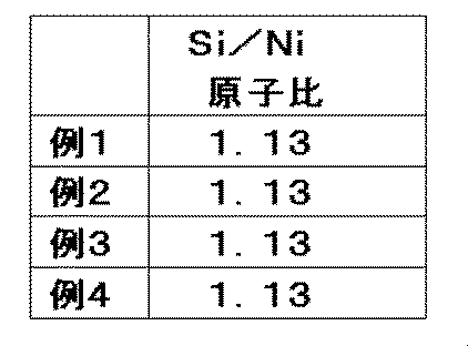
表5に評価用基板の吸収率αおよび放射率εを示す。
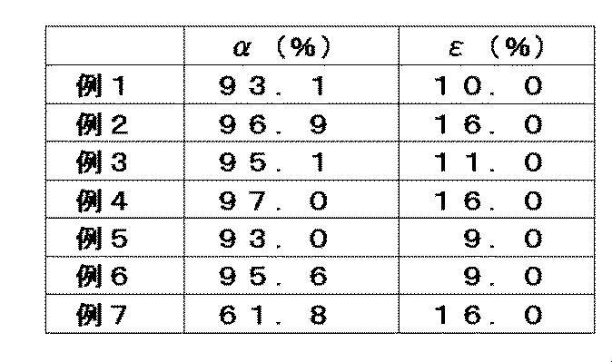
例1、3および5は、ガラス基板に光選択吸収膜を成膜した例である。吸収率αは90%以上で放射率εは11%以下である。太陽光スペクトルの波長域において低反射率を有し、赤外線スペクトルの波長域で、高反射率を有することを示している。
例2、4および6は、ステンレススチール基板に光選択吸収膜を成膜した例である。吸収率は95%以上でガラス基板上の膜よりも高い。放射率εは20%以下であり、特に例6では10%と低放射率を実現した。
これらに対し、例7は、ガラス基板に光選択吸収膜を成膜した例であり、吸収率αは61.8%で放射率εは16%である。例1および例3、例5と比較すると吸収率が低く、放射率が高くなることから、光選択性に劣る膜であるといえる。
本発明の耐熱性を示すため、例6の膜付き基材を真空中550℃、600時間保持した。保持後の吸収率αは96.0%、放射率εは9.0%であった。吸収率αは向上し、放射率εは変化しなかった。このことから真空中550℃の高温においても特性の劣化はなく、本発明の選択吸収膜は高い耐熱性を有するといえる。
また、図7に、例6を真空中550℃、600時間保持した後の波長250から25000nmまでの分光反射率を示す。波長5μmでの反射率は92.7%と90%以上となっており、これは、400℃付近の使用温度域での低い放射率を有することを示している。なお、この分光測定には、波長250~2500nmの範囲は、前述の分光測定器(HITACHI社製、商品名:U4100)を、波長2500~25000nmの範囲は、フーリエ変換赤外分光(FT-IR)測定器(Thermo Fisher Scientific社製、商品名:NICOLET6700)をそれぞれ用いた。
なお、2012年7月3日に出願された日本特許出願2012-149859号の明細書、特許請求の範囲、要約書および図面の全内容をここに引用し、本発明の明細書の開示として、取り入れるものである。
また、図7に、例6を真空中550℃、600時間保持した後の波長250から25000nmまでの分光反射率を示す。波長5μmでの反射率は92.7%と90%以上となっており、これは、400℃付近の使用温度域での低い放射率を有することを示している。なお、この分光測定には、波長250~2500nmの範囲は、前述の分光測定器(HITACHI社製、商品名:U4100)を、波長2500~25000nmの範囲は、フーリエ変換赤外分光(FT-IR)測定器(Thermo Fisher Scientific社製、商品名:NICOLET6700)をそれぞれ用いた。
なお、2012年7月3日に出願された日本特許出願2012-149859号の明細書、特許請求の範囲、要約書および図面の全内容をここに引用し、本発明の明細書の開示として、取り入れるものである。
1…パラボリックトラフ型集熱器、2…パラボリック反射鏡、3…反射鏡用支持体、4…集熱管、6…リニアフレネル型集熱器、7…第1の反射鏡、8…レシーバー、9…レシーバー用支持体、41…集熱管本体、42…光選択吸収膜、43…ガラス管、44…固定金具、81…第2の反射鏡、82…ケース部、83…ガラス板、421…赤外線反射層、422…吸収層、423…反射防止層
Claims (15)
- 基材上に形成される光選択吸収膜であって、
前記基材側から順に赤外線反射層、太陽光の吸収層および反射防止層をこの順番に有し、前記吸収層が、Cr、FeおよびNiからなる群より選択される少なくとも1種の金属元素、ケイ素および窒素を含有する金属窒化物からなり、前記金属窒化物における前記特定の金属元素、ケイ素および窒素の合計の含有量が70原子%以上であることを特徴とする光選択吸収膜。 - 前記金属窒化物の構成元素の原子比が下記式(2)および(3)の関係を満たす、請求項1に記載の光選択吸収膜。
0.7≦Si/(Cr+Fe+Ni)≦2・・・(2)
0.9≦N/(Cr+Fe+Ni)≦2.2・・・(3) - 前記金属窒化物における前記金属元素がFeとNiの少なくともいずれかからなる、請求項2に記載の光選択吸収膜。
- 前記吸収層に接する吸収補助層をさらに有し、前記吸収補助層が、CrまたはNiの少なくとも1種、Feおよびケイ素を含有する金属シリサイドからなり、
前記金属シリサイドの構成元素が原子比で下記式(5)の関係を満たす、請求項1~3のいずれか1項に記載の光選択吸収膜。
0.5≦Si/(Fe+Cr+Ni)≦1.5・・・(5) - 前記金属シリサイドがFe、NiおよびSiからなる、請求項4に記載の光選択吸収膜。
- 前記赤外線反射層が、金属単体または金属間化合物からなり、それらにおける金属元素が、Ag、Al、Au、Cu、Cr、Hf、La、Mo、Ni、Pd、Pt、Rh、Si、Ta、Ti、ZrおよびWからなる群より選択される1種以上からなる、請求項1~5のいずれか1項に記載の光選択吸収膜。
- 前記赤外線反射層が、Mo単体またはニッケルシリサイドからなる、請求項6に記載の光選択吸収膜。
- 前記ニッケルシリサイドが、原子比で下記式(6)の関係を満たす、請求項7に記載の光選択吸収膜。
0.7≦Si/Ni≦1.5・・・(6) - 前記反射防止層が、波長550nmにおける屈折率が1.9以下、かつ消衰係数が0.01以下の層であり、金属酸化物、金属酸窒化物および金属窒化物から選ばれる少なくとも1種からなる、請求項1~8のいずれか1項に記載の光選択吸収膜。
- 前記反射防止層が金属酸化物を含む層である、請求項9に記載の光選択吸収膜。
- 前記金属酸化物が、酸化ケイ素である、請求項10に記載の光選択吸収膜。
- 前記吸収層がスパッタリング法で形成された層である、請求項1~11のいずれか1項に記載の光選択吸収膜。
- 前記赤外線反射層および前記反射防止層がいずれもスパッタリング法で形成された層である、請求項1~12のいずれか1項に記載の光選択吸収膜。
- 外面に光選択吸収膜を有する集熱管本体と、前記集熱管本体の外側を囲むようにして設けられたガラス管とを有する集熱管であって、
前記光選択吸収膜が請求項1~13のいずれか1項に記載の光選択吸収膜であることを特徴とする集熱管。 - 集熱管と、前記集熱管に太陽光を集光する集光手段とを有する集熱器を備える太陽熱発電装置であって、
前記集熱管が請求項14に記載の集熱管であることを特徴とする太陽熱発電装置。
Applications Claiming Priority (2)
| Application Number | Priority Date | Filing Date | Title |
|---|---|---|---|
| JP2012149859A JP2015166637A (ja) | 2012-07-03 | 2012-07-03 | 光選択吸収膜、集熱管および太陽熱発電装置 |
| JP2012-149859 | 2012-07-03 |
Publications (1)
| Publication Number | Publication Date |
|---|---|
| WO2014007218A1 true WO2014007218A1 (ja) | 2014-01-09 |
Family
ID=49881974
Family Applications (1)
| Application Number | Title | Priority Date | Filing Date |
|---|---|---|---|
| PCT/JP2013/068056 Ceased WO2014007218A1 (ja) | 2012-07-03 | 2013-07-01 | 光選択吸収膜、集熱管および太陽熱発電装置 |
Country Status (2)
| Country | Link |
|---|---|
| JP (1) | JP2015166637A (ja) |
| WO (1) | WO2014007218A1 (ja) |
Cited By (7)
| Publication number | Priority date | Publication date | Assignee | Title |
|---|---|---|---|---|
| WO2015049977A1 (ja) * | 2013-10-02 | 2015-04-09 | 株式会社豊田自動織機 | 太陽熱集熱管及びその製造方法 |
| CN104697210A (zh) * | 2015-03-19 | 2015-06-10 | 吉林大学 | 一种原位自生长的太阳选择性吸收膜及其制备方法 |
| WO2016125393A1 (ja) * | 2015-02-06 | 2016-08-11 | 株式会社豊田自動織機 | 太陽熱集熱管、太陽光-熱変換装置及び太陽熱発電装置 |
| EP3410031A4 (en) * | 2016-01-29 | 2019-07-03 | Kabushiki Kaisha Toyota Jidoshokki | SOLAR HEAT COLLECTION TUBE |
| EP3410030A4 (en) * | 2016-01-29 | 2019-07-03 | Kabushiki Kaisha Toyota Jidoshokki | PIPE FOR OBTAINING SOLAR HEAT AND MANUFACTURING METHOD THEREFOR |
| CN111424237A (zh) * | 2020-05-20 | 2020-07-17 | 山东三齐能源有限公司 | 一种用于选择性吸收太阳光谱的膜层的制备方法 |
| US11009264B2 (en) | 2016-01-29 | 2021-05-18 | Kabushiki Kaisha Toyota Jidoshokki | Solar heat collector tube |
Families Citing this family (4)
| Publication number | Priority date | Publication date | Assignee | Title |
|---|---|---|---|---|
| JP6637748B2 (ja) * | 2015-12-02 | 2020-01-29 | 中部電力株式会社 | 遮熱膜 |
| CN106884145B (zh) * | 2016-12-28 | 2019-09-17 | 北京航空航天大学 | 一种太阳光谱选择性吸收涂层及其制备方法 |
| JP6917185B2 (ja) * | 2017-04-27 | 2021-08-11 | 中部電力株式会社 | 熱輻射抑制膜及びそれを備えた被覆部材 |
| JP6995025B2 (ja) | 2018-08-09 | 2022-02-04 | 株式会社豊田自動織機 | 太陽熱集熱管 |
Citations (5)
| Publication number | Priority date | Publication date | Assignee | Title |
|---|---|---|---|---|
| JPS5239844A (en) * | 1975-09-25 | 1977-03-28 | Agency Of Ind Science & Technol | Selective penetrating reflection film |
| JP2006214654A (ja) * | 2005-02-03 | 2006-08-17 | Nippon Electric Glass Co Ltd | 太陽熱集熱板、選択吸収膜及び太陽熱温水器 |
| JP2009198170A (ja) * | 2008-02-20 | 2009-09-03 | Schott Ag | 放射線選択的吸収コーティング、吸収チューブ、及び吸収チューブの製造方法 |
| JP2010271033A (ja) * | 2009-05-20 | 2010-12-02 | Schott Solar Ag | 放射線選択性吸収体コーティング、及び放射線選択性吸収体コーティングを処理した吸収体管 |
| JP2012506021A (ja) * | 2008-10-20 | 2012-03-08 | アベンゴア ソーラー ニュー テクノロジーズ ソシエダ アノニマ | 太陽光選択的吸収コーティング及び製造方法 |
-
2012
- 2012-07-03 JP JP2012149859A patent/JP2015166637A/ja active Pending
-
2013
- 2013-07-01 WO PCT/JP2013/068056 patent/WO2014007218A1/ja not_active Ceased
Patent Citations (5)
| Publication number | Priority date | Publication date | Assignee | Title |
|---|---|---|---|---|
| JPS5239844A (en) * | 1975-09-25 | 1977-03-28 | Agency Of Ind Science & Technol | Selective penetrating reflection film |
| JP2006214654A (ja) * | 2005-02-03 | 2006-08-17 | Nippon Electric Glass Co Ltd | 太陽熱集熱板、選択吸収膜及び太陽熱温水器 |
| JP2009198170A (ja) * | 2008-02-20 | 2009-09-03 | Schott Ag | 放射線選択的吸収コーティング、吸収チューブ、及び吸収チューブの製造方法 |
| JP2012506021A (ja) * | 2008-10-20 | 2012-03-08 | アベンゴア ソーラー ニュー テクノロジーズ ソシエダ アノニマ | 太陽光選択的吸収コーティング及び製造方法 |
| JP2010271033A (ja) * | 2009-05-20 | 2010-12-02 | Schott Solar Ag | 放射線選択性吸収体コーティング、及び放射線選択性吸収体コーティングを処理した吸収体管 |
Cited By (13)
| Publication number | Priority date | Publication date | Assignee | Title |
|---|---|---|---|---|
| WO2015049977A1 (ja) * | 2013-10-02 | 2015-04-09 | 株式会社豊田自動織機 | 太陽熱集熱管及びその製造方法 |
| CN107208934B (zh) * | 2015-02-06 | 2019-12-24 | 株式会社丰田自动织机 | 太阳能集热管、太阳光-热转换装置以及太阳能发电装置 |
| WO2016125393A1 (ja) * | 2015-02-06 | 2016-08-11 | 株式会社豊田自動織機 | 太陽熱集熱管、太陽光-熱変換装置及び太陽熱発電装置 |
| JP2016145653A (ja) * | 2015-02-06 | 2016-08-12 | 株式会社豊田自動織機 | 太陽熱集熱管、太陽光−熱変換装置及び太陽熱発電装置 |
| CN107208934A (zh) * | 2015-02-06 | 2017-09-26 | 株式会社丰田自动织机 | 太阳能集热管、太阳光‑热转换装置以及太阳能发电装置 |
| EP3255357A4 (en) * | 2015-02-06 | 2018-07-11 | Kabushiki Kaisha Toyota Jidoshokki | Solar heat collection tube, solar light/heat conversion device, and solar power generation device |
| CN104697210A (zh) * | 2015-03-19 | 2015-06-10 | 吉林大学 | 一种原位自生长的太阳选择性吸收膜及其制备方法 |
| EP3410031A4 (en) * | 2016-01-29 | 2019-07-03 | Kabushiki Kaisha Toyota Jidoshokki | SOLAR HEAT COLLECTION TUBE |
| EP3410030A4 (en) * | 2016-01-29 | 2019-07-03 | Kabushiki Kaisha Toyota Jidoshokki | PIPE FOR OBTAINING SOLAR HEAT AND MANUFACTURING METHOD THEREFOR |
| US11009264B2 (en) | 2016-01-29 | 2021-05-18 | Kabushiki Kaisha Toyota Jidoshokki | Solar heat collector tube |
| EP3410032B1 (en) * | 2016-01-29 | 2021-05-19 | Kabushiki Kaisha Toyota Jidoshokki | Solar heat collection tube |
| US11149987B2 (en) | 2016-01-29 | 2021-10-19 | Kabushiki Kaisha Toyota Jidoshokki | Solar heat collector tube and production method thereof |
| CN111424237A (zh) * | 2020-05-20 | 2020-07-17 | 山东三齐能源有限公司 | 一种用于选择性吸收太阳光谱的膜层的制备方法 |
Also Published As
| Publication number | Publication date |
|---|---|
| JP2015166637A (ja) | 2015-09-24 |
Similar Documents
| Publication | Publication Date | Title |
|---|---|---|
| JP2015166637A (ja) | 光選択吸収膜、集熱管および太陽熱発電装置 | |
| CN101900446B (zh) | 选择性辐射吸收涂层以及具有选择性辐射吸收涂层的吸收管 | |
| US9546801B2 (en) | Solar-thermal conversion member, solar-thermal conversion device, and solar thermal power generation device comprising a β-FeSi2 phase material | |
| US8555871B2 (en) | Radiation-selective absorber coating and absorber tube with said radiation-selective absorber coating | |
| JP5352267B2 (ja) | 放射線選択的吸収コーティング、吸収チューブ、及び吸収チューブの製造方法 | |
| US20150316289A1 (en) | Solar spectrum selective absorption coating and its manufacturing method | |
| US20140144426A1 (en) | Covering that selectively absorbs visible and infrared radiation, and method for the production thereof | |
| WO2016107883A1 (en) | Self-cleaning high temperature resistant solar selective structure | |
| JP2015111011A (ja) | 光選択吸収膜、集熱管、および太陽熱発電装置 | |
| Al-Rjoub et al. | W/AlSiTiNx/SiAlTiOyNx/SiAlOx multilayered solar thermal selective absorber coating | |
| EP2995882B1 (en) | Solar-thermal conversion member, solar-thermal conversion stack, solar-thermal conversion device, and solar-thermal power generating device | |
| JP2013044503A (ja) | 太陽光反射板および集光集熱装置 | |
| EP3255357B1 (en) | Solar heat collection tube, solar light/heat conversion device, and solar power generation device | |
| Platzer et al. | Absorber materials for solar thermal receivers in concentrating solar power systems | |
| Ting et al. | Sputter Deposited Nanostructured Coatings as Solar Selective Absorbers | |
| EP2677249A1 (en) | Heat receiver tube with a diffusion barrier layer | |
| WO2013180185A1 (ja) | 高反射鏡 | |
| SELVAKUMAR et al. | ÎĄŘ├┤ Í▓ ÍŞŘ Ř/December 2010 |
Legal Events
| Date | Code | Title | Description |
|---|---|---|---|
| 121 | Ep: the epo has been informed by wipo that ep was designated in this application |
Ref document number: 13812883 Country of ref document: EP Kind code of ref document: A1 |
|
| NENP | Non-entry into the national phase |
Ref country code: DE |
|
| 122 | Ep: pct application non-entry in european phase |
Ref document number: 13812883 Country of ref document: EP Kind code of ref document: A1 |
|
| NENP | Non-entry into the national phase |
Ref country code: JP |