WO2014007103A1 - 照明装置、表示装置、及びテレビ受信装置 - Google Patents
照明装置、表示装置、及びテレビ受信装置 Download PDFInfo
- Publication number
- WO2014007103A1 WO2014007103A1 PCT/JP2013/067320 JP2013067320W WO2014007103A1 WO 2014007103 A1 WO2014007103 A1 WO 2014007103A1 JP 2013067320 W JP2013067320 W JP 2013067320W WO 2014007103 A1 WO2014007103 A1 WO 2014007103A1
- Authority
- WO
- WIPO (PCT)
- Prior art keywords
- light
- optical member
- guide plate
- light guide
- transparent plate
- Prior art date
- Legal status (The legal status is an assumption and is not a legal conclusion. Google has not performed a legal analysis and makes no representation as to the accuracy of the status listed.)
- Ceased
Links
Images





Classifications
-
- G—PHYSICS
- G02—OPTICS
- G02B—OPTICAL ELEMENTS, SYSTEMS OR APPARATUS
- G02B6/00—Light guides; Structural details of arrangements comprising light guides and other optical elements, e.g. couplings
- G02B6/0001—Light guides; Structural details of arrangements comprising light guides and other optical elements, e.g. couplings specially adapted for lighting devices or systems
- G02B6/0011—Light guides; Structural details of arrangements comprising light guides and other optical elements, e.g. couplings specially adapted for lighting devices or systems the light guides being planar or of plate-like form
- G02B6/0033—Means for improving the coupling-out of light from the light guide
- G02B6/005—Means for improving the coupling-out of light from the light guide provided by one optical element, or plurality thereof, placed on the light output side of the light guide
-
- G—PHYSICS
- G02—OPTICS
- G02B—OPTICAL ELEMENTS, SYSTEMS OR APPARATUS
- G02B6/00—Light guides; Structural details of arrangements comprising light guides and other optical elements, e.g. couplings
- G02B6/0001—Light guides; Structural details of arrangements comprising light guides and other optical elements, e.g. couplings specially adapted for lighting devices or systems
- G02B6/0011—Light guides; Structural details of arrangements comprising light guides and other optical elements, e.g. couplings specially adapted for lighting devices or systems the light guides being planar or of plate-like form
- G02B6/0081—Mechanical or electrical aspects of the light guide and light source in the lighting device peculiar to the adaptation to planar light guides, e.g. concerning packaging
-
- G—PHYSICS
- G02—OPTICS
- G02F—OPTICAL DEVICES OR ARRANGEMENTS FOR THE CONTROL OF LIGHT BY MODIFICATION OF THE OPTICAL PROPERTIES OF THE MEDIA OF THE ELEMENTS INVOLVED THEREIN; NON-LINEAR OPTICS; FREQUENCY-CHANGING OF LIGHT; OPTICAL LOGIC ELEMENTS; OPTICAL ANALOGUE/DIGITAL CONVERTERS
- G02F1/00—Devices or arrangements for the control of the intensity, colour, phase, polarisation or direction of light arriving from an independent light source, e.g. switching, gating or modulating; Non-linear optics
- G02F1/01—Devices or arrangements for the control of the intensity, colour, phase, polarisation or direction of light arriving from an independent light source, e.g. switching, gating or modulating; Non-linear optics for the control of the intensity, phase, polarisation or colour
- G02F1/13—Devices or arrangements for the control of the intensity, colour, phase, polarisation or direction of light arriving from an independent light source, e.g. switching, gating or modulating; Non-linear optics for the control of the intensity, phase, polarisation or colour based on liquid crystals, e.g. single liquid crystal display cells
- G02F1/133—Constructional arrangements; Operation of liquid crystal cells; Circuit arrangements
- G02F1/1333—Constructional arrangements; Manufacturing methods
- G02F1/133308—Support structures for LCD panels, e.g. frames or bezels
-
- G—PHYSICS
- G02—OPTICS
- G02F—OPTICAL DEVICES OR ARRANGEMENTS FOR THE CONTROL OF LIGHT BY MODIFICATION OF THE OPTICAL PROPERTIES OF THE MEDIA OF THE ELEMENTS INVOLVED THEREIN; NON-LINEAR OPTICS; FREQUENCY-CHANGING OF LIGHT; OPTICAL LOGIC ELEMENTS; OPTICAL ANALOGUE/DIGITAL CONVERTERS
- G02F1/00—Devices or arrangements for the control of the intensity, colour, phase, polarisation or direction of light arriving from an independent light source, e.g. switching, gating or modulating; Non-linear optics
- G02F1/01—Devices or arrangements for the control of the intensity, colour, phase, polarisation or direction of light arriving from an independent light source, e.g. switching, gating or modulating; Non-linear optics for the control of the intensity, phase, polarisation or colour
- G02F1/13—Devices or arrangements for the control of the intensity, colour, phase, polarisation or direction of light arriving from an independent light source, e.g. switching, gating or modulating; Non-linear optics for the control of the intensity, phase, polarisation or colour based on liquid crystals, e.g. single liquid crystal display cells
- G02F1/133—Constructional arrangements; Operation of liquid crystal cells; Circuit arrangements
- G02F1/1333—Constructional arrangements; Manufacturing methods
- G02F1/1335—Structural association of cells with optical devices, e.g. polarisers or reflectors
- G02F1/1336—Illuminating devices
-
- H—ELECTRICITY
- H04—ELECTRIC COMMUNICATION TECHNIQUE
- H04N—PICTORIAL COMMUNICATION, e.g. TELEVISION
- H04N5/00—Details of television systems
- H04N5/74—Projection arrangements for image reproduction, e.g. using eidophor
- H04N5/7408—Direct viewing projectors, e.g. an image displayed on a video CRT or LCD display being projected on a screen
-
- G—PHYSICS
- G02—OPTICS
- G02B—OPTICAL ELEMENTS, SYSTEMS OR APPARATUS
- G02B6/00—Light guides; Structural details of arrangements comprising light guides and other optical elements, e.g. couplings
- G02B6/0001—Light guides; Structural details of arrangements comprising light guides and other optical elements, e.g. couplings specially adapted for lighting devices or systems
- G02B6/0011—Light guides; Structural details of arrangements comprising light guides and other optical elements, e.g. couplings specially adapted for lighting devices or systems the light guides being planar or of plate-like form
- G02B6/0081—Mechanical or electrical aspects of the light guide and light source in the lighting device peculiar to the adaptation to planar light guides, e.g. concerning packaging
- G02B6/0085—Means for removing heat created by the light source from the package
-
- G—PHYSICS
- G02—OPTICS
- G02F—OPTICAL DEVICES OR ARRANGEMENTS FOR THE CONTROL OF LIGHT BY MODIFICATION OF THE OPTICAL PROPERTIES OF THE MEDIA OF THE ELEMENTS INVOLVED THEREIN; NON-LINEAR OPTICS; FREQUENCY-CHANGING OF LIGHT; OPTICAL LOGIC ELEMENTS; OPTICAL ANALOGUE/DIGITAL CONVERTERS
- G02F1/00—Devices or arrangements for the control of the intensity, colour, phase, polarisation or direction of light arriving from an independent light source, e.g. switching, gating or modulating; Non-linear optics
- G02F1/01—Devices or arrangements for the control of the intensity, colour, phase, polarisation or direction of light arriving from an independent light source, e.g. switching, gating or modulating; Non-linear optics for the control of the intensity, phase, polarisation or colour
- G02F1/13—Devices or arrangements for the control of the intensity, colour, phase, polarisation or direction of light arriving from an independent light source, e.g. switching, gating or modulating; Non-linear optics for the control of the intensity, phase, polarisation or colour based on liquid crystals, e.g. single liquid crystal display cells
- G02F1/133—Constructional arrangements; Operation of liquid crystal cells; Circuit arrangements
- G02F1/1333—Constructional arrangements; Manufacturing methods
- G02F1/1335—Structural association of cells with optical devices, e.g. polarisers or reflectors
- G02F1/1336—Illuminating devices
- G02F1/133615—Edge-illuminating devices, i.e. illuminating from the side
-
- G—PHYSICS
- G02—OPTICS
- G02F—OPTICAL DEVICES OR ARRANGEMENTS FOR THE CONTROL OF LIGHT BY MODIFICATION OF THE OPTICAL PROPERTIES OF THE MEDIA OF THE ELEMENTS INVOLVED THEREIN; NON-LINEAR OPTICS; FREQUENCY-CHANGING OF LIGHT; OPTICAL LOGIC ELEMENTS; OPTICAL ANALOGUE/DIGITAL CONVERTERS
- G02F1/00—Devices or arrangements for the control of the intensity, colour, phase, polarisation or direction of light arriving from an independent light source, e.g. switching, gating or modulating; Non-linear optics
- G02F1/01—Devices or arrangements for the control of the intensity, colour, phase, polarisation or direction of light arriving from an independent light source, e.g. switching, gating or modulating; Non-linear optics for the control of the intensity, phase, polarisation or colour
- G02F1/13—Devices or arrangements for the control of the intensity, colour, phase, polarisation or direction of light arriving from an independent light source, e.g. switching, gating or modulating; Non-linear optics for the control of the intensity, phase, polarisation or colour based on liquid crystals, e.g. single liquid crystal display cells
- G02F1/133—Constructional arrangements; Operation of liquid crystal cells; Circuit arrangements
- G02F1/1333—Constructional arrangements; Manufacturing methods
- G02F1/1335—Structural association of cells with optical devices, e.g. polarisers or reflectors
- G02F1/1336—Illuminating devices
- G02F1/133628—Illuminating devices with cooling means
-
- G—PHYSICS
- G02—OPTICS
- G02F—OPTICAL DEVICES OR ARRANGEMENTS FOR THE CONTROL OF LIGHT BY MODIFICATION OF THE OPTICAL PROPERTIES OF THE MEDIA OF THE ELEMENTS INVOLVED THEREIN; NON-LINEAR OPTICS; FREQUENCY-CHANGING OF LIGHT; OPTICAL LOGIC ELEMENTS; OPTICAL ANALOGUE/DIGITAL CONVERTERS
- G02F2201/00—Constructional arrangements not provided for in groups G02F1/00 - G02F7/00
- G02F2201/54—Arrangements for reducing warping-twist
Definitions
- the present invention relates to a lighting device, a display device, and a television receiver.
- the liquid crystal display device requires a backlight device as a separate illumination device because the liquid crystal panel used for this does not emit light.
- a backlight device there is known an edge light type backlight device in which a light incident surface is provided on a side surface of a light guide plate, and a light source such as an LED is arranged to face the light incident surface. Yes.
- a sheet-like optical member is arranged between the light emitting surface of the light guide plate and the liquid crystal panel in order to make the light passing through the light guide plate into a planar light. Is done.
- heat generated in the vicinity of the light source is transmitted to the optical member through the light guide plate, and wrinkles may be generated on the optical member due to the heat.
- wrinkles occur on the optical member, luminance unevenness occurs in the portion of the display surface of the liquid crystal panel that overlaps with the portion where wrinkles occur, and the quality of the illumination light emitted from the light exit surface through the optical member decreases.
- Patent Document 1 discloses an edge-light type backlight device intended to prevent or suppress the occurrence of wrinkles on an optical member.
- the technology disclosed in this specification has been created in view of the above problems. In this specification, it aims at preventing or suppressing that the quality of illumination light falls by preventing or suppressing a wrinkle generating to an optical member.
- the technology disclosed in the present specification includes a light source, a light emitting surface provided on one plate surface, and a light incident surface provided on at least one side surface, and the light incident surface is the light source.
- a light guide plate that guides light from the light source to the light exit surface side, an optical member disposed on the light exit surface side of the light guide plate, and a thermal conductivity lower than that of the light guide plate It is a transparent transparent board, Comprising: It is related with an illuminating device provided with the said optical member and the transparent board distribute
- a transparent plate is disposed between the light guide plate and the optical member, whereby the light guide plate and the optical member are separated from each other.
- the transparent plate is a portion near the light incident surface (an edge on the side surface on which the light incident surface is provided) of the light emitting surface of the light guide plate, the temperature of which tends to increase due to heat generated near the light source, and the optical member. Since the transparent plate is lower in thermal conductivity than the light guide plate, the transparent plate is generated near the light source as compared with the configuration in which the light guide plate and the optical member are in contact with each other. It can be set as the structure where heat is hard to be transmitted to the optical member side.
- the transparent plate is transparent, the light emitted from the light emitting surface of the light guide plate is not blocked by the transparent plate. As a result, generation of wrinkles in the optical member due to heat generated in the vicinity of the light source can be prevented or suppressed, and deterioration of the quality of illumination light emitted through the optical member from the light emission surface can be prevented. Can be suppressed.
- the transparent plate may be in contact with the optical member and have higher rigidity than the light guide plate. According to this configuration, since the transparent plate has higher rigidity than the light guide plate, compared to the configuration in which the light guide plate and the optical member are disposed in contact with the transparent plate of the optical member. The portion is pressed with a stronger force by the transparent plate. Therefore, when wrinkles occur in the portion, the wrinkles can be leveled by being pressed by the transparent plate, and wrinkles can be eliminated. As a result, it is possible to prevent or suppress the deterioration of the quality of the illumination light.
- the transparent plate may be in contact with the light emitting surface of the light guide plate and have a lower coefficient of thermal expansion than the light guide plate. According to this configuration, since the transparent plate is less likely to thermally expand than the light guide plate, even if the light guide plate is thermally expanded toward the optical member, the transparent plate follows the light guide plate and is thermally expanded. There is nothing to do. For this reason, when the light guide plate is thermally expanded toward the optical member, the portion of the light exit surface of the light guide plate that is in contact with the transparent plate is pressed by the transparent plate. As a result, the portion of the optical member that overlaps the portion is prevented or suppressed from being pushed up to the optical member side by the light guide plate. For this reason, it can prevent thru
- the transparent plate may be arranged between the optical member and at least a frame-shaped portion that forms an edge of the light emitting surface of the light emitting surface. According to this configuration, since the frame-shaped portion that forms at least the edge of the light exit surface of the light guide plate overlaps the transparent plate, heat transfer from the light guide plate side to the optical member side is prevented or suppressed in a wide range. can do. For this reason, the heat generated in the vicinity of the light source can be more difficult to be transmitted to the optical member side. As a result, generation of wrinkles in the optical member due to heat generated in the vicinity of the light source can be further prevented or suppressed.
- the transparent plate may be disposed between the entire light emitting surface and the optical member. According to this configuration, since the transparent plate is interposed in the entire range between the light emitting surface of the light guide plate and the optical member, it is effectively prevented or suppressed that heat is transferred from the light guide plate side to the optical member side. can do. Furthermore, when the rigidity of the transparent plate is higher than that of the light guide plate and the transparent plate is disposed in contact with the light guide plate, the entire surface of the optical member is pressed by the transparent plate with a strong force. Thereby, wrinkles generated on the optical member can be leveled over the entire surface of the optical member. As a result, the generation of wrinkles in the optical member due to the heat generated in the vicinity of the light source can be further prevented or suppressed.
- a light source substrate on which a plurality of the light sources are arranged is further provided, and at least a part of a side surface of the transparent plate extends to the light source substrate side so that the extending portion is provided with the light source of the light source substrate. It may be in contact with the plate surface on the other side.
- the technology disclosed in the present specification includes the above-described illumination device, a display panel that is disposed on the opposite side of the transparent plate with the optical member interposed therebetween, and performs display using light from the light source;
- the display device comprises a frame that surrounds the optical member, is disposed between the transparent plate and the display panel, and is in contact with an edge of the transparent plate so as to contact the transparent plate. It may be a display device including a support member that supports According to this configuration, the transparent plate can be more stably arranged by supporting the transparent plate by the support member, and the transparent plate can be hardly displaced.
- the transparent plate is thermally expanded to the display panel side, so the transparent plate is difficult to move to the optical member side, so the display panel is locally pressed by the light guide plate through the optical member. This can be prevented or suppressed. As a result, it is possible to prevent or suppress deterioration of the quality of illumination light in the display device.
- the support member has a light shielding property, is interposed between the light source and an edge of the display panel, and is in contact with at least an edge of a surface of the display panel opposite to the display surface. May be. According to this configuration, since the light emitted from the light source toward the end face of the display panel is blocked by the support member, it is possible to prevent or suppress the light from entering the end face of the display panel. it can. Thereby, luminance unevenness on the display surface of the display panel due to light entering the end surface of the display panel can be prevented or suppressed.
- a display device in which the display panel is a liquid crystal panel using liquid crystal is also new and useful.
- a television receiver provided with the above display device is also new and useful.
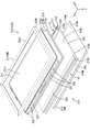
- FIG. 1 is an exploded perspective view showing a schematic configuration of a television receiver TV and a liquid crystal display unit LDU according to Embodiment 1.
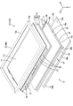
- FIG. Rear view of television receiver TV and liquid crystal display device 10 The exploded perspective view which shows schematic structure of the liquid crystal display unit LDU which comprises the liquid crystal display device 10.
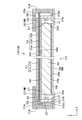
- FIG. Sectional drawing which shows the cross-sectional structure along the short side direction of the liquid crystal display device 10.
- Sectional drawing which shows the cross-sectional structure along the long side direction of the liquid crystal display device 10.
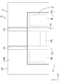
- FIG. 4 is an enlarged sectional view of the main part in the vicinity of one LED unit LU in FIG.
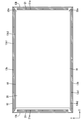
- FIG. 4 is an exploded perspective view showing a schematic configuration of a liquid crystal display unit LDU that forms a liquid crystal display device 110 according to a second embodiment.
- Sectional drawing which shows the cross-sectional structure along the short side direction of the liquid crystal display device 110
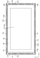
- FIG. 6 is an exploded perspective view showing a schematic configuration of a liquid crystal display unit LDU forming the liquid crystal display device 210 according to the third embodiment.
- Embodiment 1 will be described with reference to the drawings.
- a liquid crystal display device an example of a display device 10 is illustrated.
- a part of each drawing shows an X-axis, a Y-axis, and a Z-axis, and each axis direction is drawn in a common direction in each drawing.
- the Y-axis direction coincides with the vertical direction
- the X-axis direction coincides with the horizontal direction.
- the vertical direction is used as a reference for upper and lower descriptions.
- the television receiver TV includes a liquid crystal display unit LDU, various substrates PWB, MB, CTB attached to the back side (back side) of the liquid crystal display unit LDU, and main substrates PWB, MB, A cover member CV attached to cover the CTB and a stand ST are provided, and the display surface of the liquid crystal display unit LDU is held by the stand ST along the vertical direction (Y-axis direction).
- the liquid crystal display device 10 according to the present embodiment is obtained by removing at least a configuration for receiving a television signal (such as a tuner portion of the main board MB) from the television receiver TV having the above-described configuration. As shown in FIG.
- the liquid crystal display unit LDU has a horizontally long rectangular shape (rectangular shape, longitudinal shape) as a whole, and includes a liquid crystal panel 11 that is a display panel and a backlight device that is an external light source (illumination device). 1), and these are integrally held by a frame 13 and a chassis 14 which are appearance members constituting the appearance of the liquid crystal display device 10.
- the chassis 14 according to the present embodiment constitutes a part of the appearance member and a part of the backlight device 12.
- a pair of stand attachment members STA extending along the Y-axis direction are attached to two positions spaced apart in the X-axis direction on the back surface of the chassis 14 constituting the back side appearance of the liquid crystal display device 10. It has been.
- These stand attachment members STA have a substantially channel shape in which the cross-sectional shape is open on the surface on the chassis 14 side, and a pair of support columns STb in the stand ST are inserted into a space held between the stand 14 and the chassis 14. It has become.
- a wiring member (such as an electric wire) connected to an LED substrate (an example of a light source substrate) 18 included in the backlight device 12 is passed through the space in the stand attachment member STA.
- the stand ST includes a pedestal part STa that is parallel to the X-axis direction and the Z-axis direction, and a pair of column parts STb that rise from the pedestal part STa along the Y-axis direction.
- the cover member CV is made of synthetic resin, and is attached so as to cover about half of the lower side shown in FIG. 2 on the back surface of the chassis 14 while traversing the pair of stand attachment members STA in the X-axis direction. Between the cover member CV and the chassis 14, there is a component storage space that can store components such as various substrates PWB, MB, and CTB described below.
- the various substrates PWB, MB, and CTB include a power supply substrate PWB, a main substrate MB, and a control substrate CTB.
- the power supply substrate PWB can be said to be a power supply source of the liquid crystal display device 10 and supplies driving power to the other substrates MB and CTB and the LED (an example of a light source) 17 included in the backlight device 12. It is possible. Therefore, it can be said that the power supply substrate PWB also serves as the “LED drive substrate for driving the LED 17”.
- the main board MB has at least a tuner unit capable of receiving a television signal and an image processing unit (not shown) for processing the received television signal, and controls the processed image signal as follows. Output to the substrate CTB is possible.
- the main board MB receives an image signal from the image reproduction device when the liquid crystal display device 10 is connected to an external image reproduction device (not shown). It can be processed and output to the control board CTB.
- the control board CTB has a function of converting an image signal input from the main board into a liquid crystal driving signal and supplying the converted liquid crystal driving signal to the liquid crystal panel 11.
- the liquid crystal display unit LDU that constitutes the liquid crystal display device 10 has its main components between a frame 13 that forms the front side appearance and a chassis 14 that forms the back side appearance. It is assumed that it is housed in a space.
- the main components housed in the frame 13 and the chassis 14 include at least the liquid crystal panel 11, the optical member 15, the transparent plate 30, the light guide plate 16, and the LED unit LU. Among these, the liquid crystal panel 11, the optical member 15, the transparent plate 30, and the light guide plate 16 are held in a state of being sandwiched between the front frame 13 and the back chassis 14 in a stacked state. It has become.
- the backlight device 12 includes an optical member 15, a transparent plate 30, a light guide plate 16, an LED unit LU, and a chassis 14, and is configured by removing the liquid crystal panel 11 and the frame 13 from the liquid crystal display unit LDU. .
- a pair of LED units LU forming the backlight device 12 are arranged in the frame 13 and the chassis 14 so as to sandwich the light guide plate 16 from both sides in the short side direction (Y-axis direction).
- the LED unit LU includes an LED 17 that is a light source and an LED substrate 18 on which the LED 17 is mounted.
- the liquid crystal panel 11 has a horizontally long rectangular shape (rectangular shape, longitudinal shape) in a plan view, and a pair of glass substrates 11a and 11b (see FIG. 4) having excellent translucency. ) Are bonded together with a predetermined gap therebetween, and liquid crystal is sealed between the substrates 11a and 11b.
- One substrate (array substrate) 11b is provided with a switching element (for example, TFT) connected to a source wiring and a gate wiring orthogonal to each other, a pixel electrode connected to the switching element, an alignment film, and the like.
- a switching element for example, TFT
- the other substrate (CF substrate) 11a has a color filter, a counter electrode, an alignment film, and the like in which colored portions such as R (red), G (green), and B (blue) are arranged in a predetermined arrangement. Is provided.
- the liquid crystal panel 11 is placed on the front side of the optical member 15 to be described below, and the back side surface (the outer surface of the polarizing plate on the back side) is in close contact with the optical member 15 with almost no gap. . This prevents dust and the like from entering between the liquid crystal panel 11 and the optical member 15.
- the display surface 11c of the liquid crystal panel 11 includes a display area on the center side of the screen where images can be displayed, and a non-display area having a frame shape (frame shape) surrounding the display area on the outer peripheral edge side of the screen.
- the liquid crystal panel 11 is connected to a control board CTB via a driver component for driving liquid crystal and a flexible board 26, and an image is displayed in a display area on the display surface 11c based on a signal input from the control board CTB. It has come to be.
- a polarizing plate (not shown) is disposed outside each of the substrates 11a and 11b.
- the optical member 15 has a horizontally long rectangular shape when viewed from the same plane as the liquid crystal panel 11, and the size (short side dimension and long side dimension) is the same as that of the liquid crystal panel 11. Is done.
- the optical member 15 is placed so as to be laminated on the surface of a transparent plate 30 to be described later, and is arranged in a state of being sandwiched between the liquid crystal panel 11 and the transparent plate 30 described above.
- Each of the optical members 15 is in the form of a sheet and three are stacked on top of each other. Specifically, the diffusion sheet 15a, the lens sheet (prism sheet) 15b, and the reflective polarizing sheet 15c are sequentially formed from the back side (light guide plate 16 side). Note that the three sheets 15a, 15b, and 15c have substantially the same size in a plan view.
- the light guide plate 16 is made of a synthetic resin material (acrylic resin such as PMMA, polycarbonate, etc.) having a refractive index sufficiently higher than air and substantially transparent (excellent translucency). As shown in FIG. 3, the light guide plate 16 has a horizontally long rectangular shape in a plan view and is thicker than the optical member 15 and the transparent plate 30, as with the liquid crystal panel 11, the optical member 15, and the transparent plate 30.
- the long side direction on the principal surface coincides with the X-axis direction
- the short side direction coincides with the Y-axis direction
- the plate thickness direction orthogonal to the principal surface coincides with the Z-axis direction.
- the light guide plate 16 is laminated on the back side of the transparent plate 30 and is disposed so as to be sandwiched between the transparent plate 30 and the chassis 14. As shown in FIG. 4, the light guide plate 16 has at least the short side dimension larger than the short side direction dimensions of the liquid crystal panel 11, the optical member 15, and the transparent plate 30, and both ends in the short side direction. The portions (both side surfaces on the long side) are arranged so as to coincide with both end portions of the liquid crystal panel 11 and the optical member 15 (so as to overlap in plan view).
- the light guide plate 16 is disposed in a form sandwiched in the Y-axis direction by a pair of LED units LU disposed on both sides in the short side direction, and light from the LED 17 is respectively received at both ends in the short side direction.
- the light guide plate 16 has a function of raising and emitting the light from the LED 17 introduced from both ends in the short side direction so as to face the optical member 15 side (front side) while propagating inside.
- the backlight device 12 according to the present embodiment has a configuration in which the LED 17 that is a light source is arranged to face the side surface of the light guide plate 16 and the light that has passed through the light guide plate 16 is directed toward the liquid crystal panel 11.
- edge light type side light type
- the surface facing the front side (the surface facing the optical member 15) emits light from the inside toward the transparent plate 30, the optical member 15, and the liquid crystal panel 11. It has become.
- both end faces on the long side that are long along the X-axis direction (both end faces that the both ends in the short side direction have) are LEDs 17 ( The LED board 18) and the LED board 18) are opposed to each other with a predetermined space therebetween, and these form a pair of light incident surfaces 16b on which light emitted from the LEDs 17 is incident.
- the reflection sheet 20 is disposed so as to be sandwiched between the chassis 14 and the light guide plate 16, and can reflect the light emitted from the opposite surface 16 c of the light guide plate 16 to the outside on the back side and rise to the front side. It has become.
- the reflection sheet 20 is made of a synthetic resin and has a white surface with excellent light reflectivity.
- the short side dimension of the reflection sheet 20 matches the short side dimension of the light guide plate 16.
- the LED 17 constituting the LED unit LU has a configuration in which an LED chip (not shown) is sealed with a resin material on a substrate portion fixed to the LED substrate 18.
- the LED chip mounted on the substrate unit has one main emission wavelength, and specifically, one that emits blue light in a single color is used.
- the resin material that seals the LED chip is dispersed and blended with a phosphor that emits a predetermined color when excited by the blue light emitted from the LED chip, and generally emits white light as a whole. It is said.
- the phosphor for example, a yellow phosphor that emits yellow light, a green phosphor that emits green light, and a red phosphor that emits red light are used in appropriate combination, or any one of them is used. It can be used alone.
- the LED 17 is of a so-called top surface light emitting type in which a surface opposite to the mounting surface 18a with respect to the LED substrate 18 (a surface facing the light incident surface 16b of the light guide plate 16) is a main light emitting surface.
- the LED board 18 constituting the LED unit LU has a long and narrow plate shape extending along the long side direction of the light guide plate 16 (X-axis direction, long side direction of the light incident surface 16b).
- the plate surface is accommodated in the frame 13 and the chassis 14 in a posture parallel to the X-axis direction and the Z-axis direction, that is, a posture parallel to the light incident surface 16 b of the light guide plate 16.
- the LED substrate 18 has a length dimension that is approximately half of the long side dimension of the light guide plate 16.
- the LED 17 having the above-described configuration is surface-mounted on the inner side of the LED substrate 18, that is, the plate surface facing the light guide plate 16 side (the surface facing the light guide plate 16), and this is the mounting surface 18 a.
- a plurality of LEDs 17 are arranged in a line (linearly) in parallel on the mounting surface 18a of the LED substrate 18 along the length direction (X-axis direction) with a predetermined interval. That is, it can be said that a plurality of LEDs 17 are intermittently arranged in parallel along the long side direction at both ends on the long side of the backlight device 12.
- the interval between the LEDs 17 adjacent to each other in the X-axis direction, that is, the arrangement pitch of the LEDs 17 is substantially equal.
- the arrangement direction of the LEDs 17 coincides with the long side direction (X-axis direction) of the LED substrate 18.
- a wiring pattern (not shown) made of a metal film (such as a copper foil) that extends along the X-axis direction and connects the adjacent LEDs 17 across the LED 17 group in series.
- the terminal portions formed at both ends of the wiring pattern are connected to the power supply substrate PWB via wiring members such as connectors and electric wires, so that driving power is supplied to each LED 17. It has become.
- Both the frame 13 and the chassis 14 are made of metal such as aluminum, for example, and mechanical strength (rigidity) and thermal conductivity are both higher than when the frame 13 and the chassis 14 are made of synthetic resin.
- the frame 13 and the chassis 14 are stacked on each other while accommodating the LED units LU paired at both ends (both ends on both long sides) in the short side direction.
- the liquid crystal panel 11, the optical member 15, the transparent plate 30, and the light guide plate 16 are accommodated so as to be sandwiched from the front side and the back side.
- the frame 13 has a horizontally long frame shape as a whole so as to surround the display area on the display surface 11 c of the liquid crystal panel 11.
- the frame 13 includes a panel pressing portion 13a that is parallel to the display surface 11c of the liquid crystal panel 11 and presses the liquid crystal panel 11 from the front side, and a side plate portion 13b that protrudes from the outer peripheral side portion of the panel pressing portion 13a toward the back side.
- the cross-sectional shape is substantially L-shaped.
- the panel pressing portion 13a forms a horizontally long frame shape following the outer peripheral side portion (non-display area, frame portion) of the liquid crystal panel 11, and presses the outer peripheral side portion of the liquid crystal panel 11 from the front side over almost the entire circumference. Is possible.
- the panel pressing portion 13a includes an optical member 15, a transparent plate 30, and an outer peripheral portion of the light guide plate 16, which are arranged on the outer side in the radial direction than the outer peripheral portion of the liquid crystal panel 11.
- each LED unit LU has a width that can cover the front side.
- the outer surface of the panel pressing portion 13a facing the front side (the surface opposite to the surface facing the liquid crystal panel 11) is exposed to the outside on the front side of the liquid crystal display device 10 like the display surface 11c of the liquid crystal panel 11.
- the front surface of the liquid crystal display device 10 is configured together with the display surface 11 c of the panel 11.
- the side plate portion 13b has a substantially rectangular tube shape protruding from the outer peripheral side portion (specifically, the outer peripheral end portion) of the panel pressing portion 13a toward the back side, and a pair of divided frames constituting the long side of the frame 13 And the pair of divided frames constituting the short side of the frame 13 have different widths of the side plate portions 13b.
- the side plate portion 13b extending from the pair of divided frames constituting the long side of the frame 13 is larger in width than the side plate portion 13b extending from the pair of divided frames constituting the short side of the frame 13.
- the side plate portion 13b surrounds the liquid crystal panel 11, the optical member 15, the transparent plate 30, the light guide plate 16, and the respective LED units LU accommodated therein.
- the side plate portion 13b has an outer surface along the circumferential direction in the liquid crystal display device 10 exposed to the outside in the circumferential direction of the liquid crystal display device 10, and constitutes a top surface, a bottom surface, and both side surfaces of the liquid crystal display device 10.
- a pressing protrusion 24 that protrudes to the back side, that is, the liquid crystal panel 11 side, is integrally formed on the inner edge portion of the panel pressing portion 13 a.
- a cushioning material 24a is attached to the projecting tip surface of the pressing projection 24 (see FIG. 6), and the liquid crystal panel 11 can be pressed from the front side via the cushioning material 24a.
- the cushioning material 24a is provided in each frame constituting the frame 13 so as to extend along each side, but is divided for each side, and when the divided frames are assembled, As described above, the frame shape is arranged over the entire circumference at the inner peripheral edge of the panel pressing portion 13a.
- a screw attachment portion 21 to which a screw member SM is attached is provided at a position closer to the inner side than the side plate portion 13b (closer to the light guide plate 16), as shown in FIG. It is integrally formed.
- the screw attachment portion 21 protrudes from the inner surface of the panel pressing portion 13a toward the back side along the Z-axis direction, and extends along each side (X-axis direction or Y-axis direction) of the panel pressing portion 13a. It has an almost block shape.
- the screw attachment portion 21 is formed with a groove portion 21 a that opens toward the back side and that can tighten the screw member SM.
- the side plate portion 13 b surrounds the liquid crystal panel 11, the optical member 15, the light guide plate 16, and each LED unit LU accommodated therein, and is sized to contact the outer peripheral surface of the chassis 14 disposed on the back side. Yes.
- the side plate portion 13b has an outer surface along the circumferential direction in the liquid crystal display device 10 exposed to the outside in the circumferential direction of the liquid crystal display device 10, and constitutes a top surface, a bottom surface, and both side surfaces of the liquid crystal display device 10.
- the side plate portion 13b protrudes from the inner surface of the panel pressing portion 13a toward the back side along the Z-axis direction at the outer end portion of the panel pressing portion 13a, and each side (X-axis direction or Y-axis) of the panel pressing portion 13a. It is in the shape of a horizontally long, substantially block extending along the direction.
- the side plate portion 13b is in contact with the outer end portion of the second bottom plate portion 14b of the chassis 14 to be described later.
- the screw member SM described above is attached to the side plate portion 13b (hereinafter, the side plate portions 13b extending from the pair of divided frames). (Referred to as the side plate portion 13b on the long side). Therefore, as shown in FIG. 4, the long side side plate portion 13b is formed with a groove portion 13b1 that opens toward the back side and can fasten the screw member SM. In addition, the long-side side plate portion 13b is provided with a substrate attachment portion 13b2 in such a manner that the tip protruding to the back side slightly extends inward. A plate surface opposite to the mounting surface 18a of the LED substrate 18 is attached to the front end surface of the substrate attachment portion 13b2. As a result, the LED substrate 18 is held on the chassis 14 with its mounting surface 18 a parallel to the light incident surface 16 b of the light guide plate 16.
- a space capable of accommodating the printed board 27 is provided between the long side side plate portion 13 b and the LED board 18.
- a plurality of flexible boards 26 are intermittently arranged along the long side direction of the printed board 27, and the other end portions are connected to the printed board 27, respectively.
- the printed circuit board 27 has a connector portion (not shown) connected to one end side of the FPC (not shown), and an FPC insertion hole (not shown) formed in the chassis 14 at the other end side of the FPC. ) Through the outside of the chassis 14 and connected to the control board CTB.
- the chassis 14 has a generally horizontally shallow shallow plate shape as a whole so as to cover the light guide plate 16, the LED unit LU, and the like over almost the entire region from the back side.
- the outer surface of the chassis 14 facing the back side (the surface opposite to the surface facing the light guide plate 16 and the LED unit LU) is exposed outside the back side of the liquid crystal display device 10 and constitutes the back surface of the liquid crystal display device 10. is doing.
- the chassis 14 has a horizontally elongated first bottom plate portion 14a, and protrudes from the both long side end portions of the first bottom plate portion 14a to the back side in a stepped manner, and the LED unit LU is arranged. And a pair of second bottom plate portions 14b.
- the first bottom plate portion 14 a has a flat plate shape capable of receiving the short side of the light guide plate 16 from the back side, and constitutes a receiving portion for the light guide plate 16. It can be said.
- both end portions in the long side direction extend outward from both end portions in the long side direction of the light guide plate 16, as shown in FIG.
- the above-described screw member SM for fixing the frame 13 and the chassis 14 in the assembled state is a pair of parts to be mounted from the outside.
- the first bottom plate portion 14 a has tip portions at both ends in the long side direction (X-axis direction) in contact with the inner surface of the side plate portion 13 b, whereby the chassis 14 is positioned with respect to the frame 13 in the X-axis direction. Has been.
- the second bottom plate portion 14 b can be disposed with the LED unit LU by retracting to the back side of the first bottom plate portion 14 a.
- the second bottom plate portion 14b is parallel to the first bottom plate portion 14a, and the LED substrate is disposed so as to be perpendicular to the inner surface thereof. Further, as described above, at the outer end of the second bottom plate portion 14b, the inner surface is in contact with the tip of the side plate portion 13b on the long side, and the screw member SM is mounted from the outside.
- the transparent plate 30 is made of a material (glass or the like) that is different from the light guide plate 16 and has a refractive index sufficiently higher than that of air and is almost transparent (excellent in translucency). Specifically, the transparent plate 30 has a lower thermal conductivity than the light guide plate 16, has a higher rigidity than the light guide plate 16, and has a lower thermal expansion coefficient than the light guide plate 16. As shown in FIG. 3, the transparent plate 30 has a horizontally long rectangular shape in a plan view and has a thickness smaller than that of the light guide plate 16, similar to the liquid crystal panel 11, the optical member 15, and the light guide plate 16.
- the long side direction on the main surface thereof coincides with the X-axis direction
- the short side direction thereof coincides with the Y-axis direction
- the plate thickness direction orthogonal to the main surface coincides with the Z-axis direction.
- the transparent plate 30 is laminated on the front side of the light guide plate 16, that is, on the light emitting surface 16 a side, and is disposed so as to be sandwiched between the light guide plate 16 and the optical member 15.
- the back surface of the transparent plate 30 is in contact with the entire surface of the light emitting surface 16a of the light guide plate 16 (see FIG. 7), and the surface thereof is in contact with the entire back surface of the optical member 15.
- the transparent plate 30 By arranging the transparent plate 30 in such a manner, the light emitting surface 16b of the light guide plate 16 and the optical member 15 are separated from each other. Since the transparent plate 30 is transparent like the light guide plate 16, the light emitted from the light emitting surface 16 a and traveling toward the optical member 15 and the liquid crystal panel 11 is not blocked by the transparent plate 30.
- the length of the transparent plate 30 in the short side direction is larger than the length in the short side direction of each of the optical member 15 and the light guide plate 16.
- Both end portions (both side surfaces forming the long side) of the optical member 15 and the light guide plate 16 extend outside the both end portions in the respective short side directions (outside the light incident surface 16b) (hereinafter referred to as the light incident surface 16b).
- the extending portion is referred to as an extending portion 30a).
- the extending portion 30 a extends to the LED substrate 18 side, and the tip thereof is in contact with the mounting surface 18 a of the LED substrate 18.
- the extending portion 30 a of the transparent plate 30 is interposed between the LED 17 and the optical member 15, so that the heat is prevented or suppressed from being directly transmitted from the LED 17 to the optical member 15 side by the extending portion 30 a. ing. Furthermore, even when the LED substrate 18 is warped due to heat, the LED portion 18 is restricted from warping to the light incident surface 16b side by the extending portion 30a. Therefore, the LED 17 and the light incident surface 16b The distance between the two is maintained constant.
- the transparent plate 30 is disposed on the light emitting surface 16b side of the light guide plate 16, and the transparent plate 30 is at least on the light incident surface 16b side of the optical member 15 and the light emitting surface 16b1. It is the structure interposed between the edge 16a1 of this.
- the heat generated in the vicinity of the LED 17 is transmitted to the light incident surface 16b of the light guide plate 16, and the temperature in the vicinity of the light incident surface 16b of the light guide plate 16 increases.
- the transparent plate 30 is arranged in the above-described manner, so that the light emission surface 16a and the optical member 15 are separated from each other.
- the heat conductivity is lower than that of the light guide plate 16
- the heat accumulated in the vicinity of the light incident surface 16b is transmitted from the edge on the light incident surface 16b side to the optical member 15 side in the light emitting surface 16a. It is prevented or suppressed by 30 so that heat is hardly transmitted to the optical member 15 side.
- the transparent plate 15 is disposed in contact with the entire surface of the light emitting surface 16b of the light guide plate 16, even if the temperature of the portion other than the vicinity of the light incident surface 16b in the light guide plate 16 rises, The transparent plate 30 prevents or suppresses heat from being transmitted from the light emitting surface 16a to the optical member 15 side.
- the optical member 15 since the transparent plate 30 is higher in rigidity than the light guide plate 16, the optical member 15 has a stronger force than the configuration in which the optical member 15 is disposed in contact with the light emitting surface 16b of the light guide plate 16. The entire back surface of the member 15 is pressed by the transparent plate 30. When the optical member 15 is pressed with such a strong force, the wrinkles on the optical member 15 are leveled, and the wrinkles on the optical member 15 are eliminated. Further, since the transparent plate 30 has a lower coefficient of thermal expansion than the light guide plate 16, the amount of displacement due to thermal expansion is smaller than that of the light guide plate 16.
- the optical member 15 is disposed in contact with the light guide plate 16
- the optical member 15 is locally pressed as the light guide plate 16 thermally expands toward the optical member 15.
- the transparent plate 30 having a smaller displacement than the light guide plate 16 is interposed between the light guide plate 16 and the optical member 15, the light guide plate 16 is thermally expanded toward the optical member 15 side. Even if it exists, it is prevented thru
- the transparent plate 30 is disposed between the light guide plate 16 and the optical member 15 so that the light guide plate 16 and the optical member 15 are separated from each other.
- the transparent plate 30 is a portion of the light exit surface 16a of the light guide plate 16 in the vicinity of the light incident surface 16b whose temperature is likely to rise due to heat generated in the vicinity of the LED 17 (the edge on the side surface side where the light incident surface 16b is provided).
- the optical member 15, and the transparent plate 30 has a lower thermal conductivity than the light guide plate 16, so that the light guide plate 16 and the optical member 15 are in contact with each other.
- the heat generated in the vicinity of the LED 17 can be made difficult to be transmitted to the optical member 15 side.
- the transparent plate 30 is transparent, the light emitted from the light emitting surface 16 b of the light guide plate 16 is not blocked by the transparent plate 30.
- generation of wrinkles in the optical member 15 due to heat generated in the vicinity of the LED 17 can be prevented or suppressed, and the quality of illumination light emitted from the light emitting surface 16a via the optical member 15 is reduced. Can be prevented or suppressed.
- the transparent plate 30 is in contact with the optical member 15 and has higher rigidity than the light guide plate 16.
- the transparent plate 30 is more transparent than the configuration in which the light guide plate 16 and the optical member 15 are in contact with each other in the portion of the optical member 15 that contacts the transparent plate 30.
- the part is pressed with a strong force. Therefore, when wrinkles occur in the portion, the wrinkles can be leveled by being pressed by the transparent plate 30, and the wrinkles can be eliminated. As a result, it is possible to prevent or suppress the deterioration of the quality of the illumination light.
- the transparent plate 30 is in contact with the light emitting surface 16 a of the light guide plate 16 and has a lower coefficient of thermal expansion than the light guide plate 16. With such a configuration, the transparent plate 30 is less likely to thermally expand than the light guide plate 16, so even if the light guide plate 16 is thermally expanded toward the optical member 15, the transparent plate 30 is transparent. The plate 30 does not thermally expand following the light guide plate 16. For this reason, when the light guide plate 16 is thermally expanded toward the optical member 15, a portion of the light emitting surface 16 a of the light guide plate 16 that is in contact with the transparent plate 30 is pressed by the transparent plate 30.
- the transparent plate 30 is disposed between the entire surface of the light emitting surface 16a and the optical member 15.
- the transparent plate 30 is interposed in the entire range between the light emitting surface 16a of the light guide plate 16 and the optical member 15, so that the optical member 15 side from the light guide plate 16 side. It is possible to effectively prevent or suppress the transfer of heat to the heat.
- the rigidity of the transparent plate 30 is higher than that of the light guide plate 16 and the transparent plate 30 is arranged in contact with the light guide plate 16, the entire surface of the optical member 15 is pressed by the transparent plate 30 with a strong force. Will be. Thereby, wrinkles generated on the optical member 15 can be leveled over the entire surface of the optical member 15. As a result, generation of wrinkles in the optical member 15 due to heat generated in the vicinity of the LED 17 can be further prevented or suppressed.
- the extending portions 30a extending from the position overlapping the light incident surface 16b to the LED substrate 18 side are provided on both side surfaces forming the long side of the transparent plate 30. Yes.
- the extended portion 30 a is in contact with the mounting surface 18 a of the LED substrate 18.
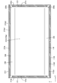
- the transparent plate 130 has a frame shape.
- the frame-shaped transparent plate 130 is in contact with a frame-shaped portion that forms the edge of the light emitting surface 116a in the light emitting surface 116a. Therefore, it can be said that the transparent plate 130 is disposed between the optical member 115 and the edge of at least the light incident surface 116b side of the light emitting surface 116a. Even in such a configuration, the light guide plate 116 and the optical member 115 are separated from each other by the transparent plate 130, and the transparent plate 130 has a thermal conductivity higher than that of the light guide plate 116.
- the heat generated in the vicinity of the LED 117 is less likely to be transmitted to the optical member 115 side as compared with the configuration in which the light guide plate 116 and the optical member 115 are disposed in contact with each other.
- generation of wrinkles in the optical member 115 due to heat generated in the vicinity of the LED 117 can be prevented or suppressed, and the quality of illumination light emitted from the light emitting surface 116a via the optical member 115 is reduced. Can be prevented or suppressed.
- Embodiment 3 will be described with reference to the drawings.
- the shape of the transparent plate 230 is different from that in the first and second embodiments. Since the other configuration is the same as that of the first embodiment, the description of the structure, operation, and effect is omitted.
- FIGS. 11 and 12 the portions obtained by adding the numeral 200 to the reference numerals in FIGS. 3 and 7 are the same as the portions described in the first embodiment.
- a pair of optical members 230 and 230 are arranged on the light emitting surface 216 b side of the light guide plate 216.
- These transparent plates 230 have the same shape, and are in contact with both ends of the optical member 215 and the light emitting surface 216a on the light incident surface 216b side. Even in such a configuration, the light guide plate 216 and the optical member 215 are separated from each other by the transparent plate 230, and the transparent plate 230 has a thermal conductivity higher than that of the light guide plate 216.
- the heat generated in the vicinity of the LED 217 is less likely to be transmitted to the optical member 215 side as compared to the configuration in which the light guide plate 216 and the optical member 215 are in contact with each other.
- generation of wrinkles in the optical member 215 due to heat generated in the vicinity of the LED 217 can be prevented or suppressed, and the quality of illumination light emitted from the light emitting surface 216a via the optical member 215 is reduced. Can be prevented or suppressed.
- Embodiment 4 will be described with reference to the drawings.
- the fourth embodiment differs from that of the first embodiment in that it further includes a support member 332. Since the other configuration is the same as that of the first embodiment, the description of the structure, operation, and effect is omitted.
- FIG. 13 the part obtained by adding the numeral 300 to the reference numeral in FIG. 4 is the same as the part described in the first embodiment.
- the backlight device 312 has a frame shape whose inner edge is slightly larger than the optical member 315, and is placed on the side surface facing the front side of the LED substrate 318.
- a plate-like support member 332 is provided so as to surround the optical member 315.
- the size of the liquid crystal panel 311 in plan view is slightly larger than that of the optical member 315 and the light guide plate 316.
- the support member 332 is sandwiched between the edge of the liquid crystal panel 311 and the edge of the transparent plate 330 and is in contact with the edge of the transparent plate 330. As a result, the support member 332 supports the edge of the transparent plate 330.
- the transparent plate 330 by supporting the transparent plate 330 by the support member 332 in this way, the transparent plate 330 can be arranged more stably, and the transparent plate 330 can be hardly displaced. Thereby, even if the transparent plate 330 is thermally expanded to the liquid crystal panel 311 side, the transparent plate 330 is difficult to move to the optical member 315 side. Therefore, the liquid crystal panel 311 is guided to the light guide plate via the optical member 315. It is possible to prevent or suppress local pressing by 316. As a result, it is possible to prevent or suppress the deterioration of the quality of the illumination light in the liquid crystal display device 310.
- the support member 332 has a light shielding property, and is interposed between the LED 317 and the edge of the liquid crystal panel 311 by coming into contact with the edge of the liquid crystal panel 311.
- the support member 332 With such a configuration, the light emitted from the LED 317 toward the end surface of the liquid crystal panel 311 is blocked by the support member 332, so that the light is incident on the end surface of the liquid crystal panel 311. Intrusion can be prevented or suppressed. Thereby, luminance unevenness on the display surface 311c of the liquid crystal panel 311 due to light entering the end surface of the liquid crystal panel 311 can be prevented or suppressed.
- the transparent plate is disposed in contact with the light emitting surface of the light guide plate and the back surface of the optical member.
- the transparent plate has at least one of the light emitting surfaces. What is necessary is just to be distribute
- liquid crystal display device that does not include a cabinet is illustrated, but a liquid crystal display device that includes a cabinet may be used.
- the extending portions provided on both side surfaces on the long side of the transparent plate are exemplified as contacting the mounting surface of the LED substrate.
- substrate may be sufficient.
- the extending portion may not be provided on the transparent plate, and both long side surfaces of the transparent plate and the light incident surface of the light guide plate may coincide with each other in the Z-axis direction.
- the configuration, arrangement, shape, material, and the like of the transparent plate can be changed as appropriate.
Landscapes
- Physics & Mathematics (AREA)
- General Physics & Mathematics (AREA)
- Optics & Photonics (AREA)
- Nonlinear Science (AREA)
- Mathematical Physics (AREA)
- Chemical & Material Sciences (AREA)
- Crystallography & Structural Chemistry (AREA)
- Engineering & Computer Science (AREA)
- Multimedia (AREA)
- Signal Processing (AREA)
- Planar Illumination Modules (AREA)
- Liquid Crystal (AREA)
Abstract
バックライト装置12は、LED17と、表側の板面に設けられた光出射面16aと、対辺を構成する一対の側面にそれぞれ設けられた一対の光入射面16b,16bと、を有し、光入射面16bがLED17と対向し、LED17からの光を光出射面16a側に導光する導光板16と、導光板16の光出射面16a側に配された光学部材15と、導光板16よりも熱伝導率が低い透明な透明板30であって、光学部材15と光出射面16aの少なくとも光入射面16b側の端縁との間に配された透明板30と、を備える。
Description
本発明は、照明装置、表示装置、及びテレビ受信装置に関する。
近年、テレビ受信装置をはじめとする画像表示装置の表示素子は、従来のブラウン管から液晶パネルやプラズマディスプレイパネルなどの薄型表示素子を適用した薄型表示装置に移行しつつあり、画像表示装置の薄型化を可能としている。液晶表示装置は、これに用いる液晶パネルが自発光しないため、別途に照明装置としてバックライト装置を必要としている。このようなバックライト装置の一例として、導光板の側面に光入射面が設けられ、その光入射面と対向する形でLED等の光源が配されたエッジライト型のバックライト装置が知られている。
エッジライト型のバックライト装置を備える液晶表示装置では、導光板を通過した光を面状の光とするために、導光板の光出射面と液晶パネルとの間にシート状の光学部材が配される。このような光学部材を備える液晶表示装置では、光源近傍に発生した熱が導光板を介して光学部材へと伝わり、その熱によって光学部材上に皺が発生することがある。光学部材上に皺が発生すると、皺が発生した部位と重畳する液晶パネルの表示面の部位に輝度ムラが発生し、光出射面から光学部材を介して出射される照明光の品位が低下する。このように光学部材上に皺が発生することを防止ないし抑制することを目的としたエッジライト型のバックライト装置が、例えば特許文献1に開示されている。
(発明が解決しようとする課題)
しかしながら、特許文献1の液晶表示装置では、光学部材が導光板の光出射面と当接した構成となっているため、光源近傍に発生した熱が導光板を介して光学部材へと伝わり易い構成となっている。このため、光源近傍に発生した熱による光学部材への影響を十分に回避することが難しく、熱によって光学部材上に発生する皺を十分に防止ないし抑制することができない。
しかしながら、特許文献1の液晶表示装置では、光学部材が導光板の光出射面と当接した構成となっているため、光源近傍に発生した熱が導光板を介して光学部材へと伝わり易い構成となっている。このため、光源近傍に発生した熱による光学部材への影響を十分に回避することが難しく、熱によって光学部材上に発生する皺を十分に防止ないし抑制することができない。
本明細書で開示される技術は、上記の課題に鑑みて創作されたものである。本明細書では、光学部材に皺が発生することを防止ないし抑制することで、照明光の品位が低下することを防止ないし抑制することを目的とする。
(課題を解決するための手段)
本明細書で開示される技術は、光源と、一方の板面に設けられた光出射面と、少なくとも一つの側面に設けられた光入射面と、を有し、前記光入射面が前記光源と対向し、前記光源からの光を前記光出射面側に導光する導光板と、前記導光板の前記光出射面側に配された光学部材と、前記導光板よりも熱伝導率が低い透明な透明板であって、前記光学部材と前記光出射面の少なくとも前記光入射面側の端縁との間に配された透明板と、を備える照明装置に関する。
本明細書で開示される技術は、光源と、一方の板面に設けられた光出射面と、少なくとも一つの側面に設けられた光入射面と、を有し、前記光入射面が前記光源と対向し、前記光源からの光を前記光出射面側に導光する導光板と、前記導光板の前記光出射面側に配された光学部材と、前記導光板よりも熱伝導率が低い透明な透明板であって、前記光学部材と前記光出射面の少なくとも前記光入射面側の端縁との間に配された透明板と、を備える照明装置に関する。
上記の照明装置では、導光板と光学部材との間に透明板が配されることで導光板と光学部材との間が離間した構成とされる。ここで、透明板は導光板の光出射面のうち光源近傍に発生した熱によって温度が上昇し易い光入射面近傍の部位(光入射面が設けられた側面側の端縁)と光学部材との間に配され、かつ、透明板は導光板よりも熱伝導率が低いものとされているので、導光板と光学部材とが当接して配された構成に比して光源近傍に発生した熱が光学部材側へ伝わり難い構成とすることができる。また、透明板は透明とされているので、導光板の光出射面から出射された光が透明板によって遮られることはない。この結果、光源近傍に発生した熱によって光学部材に皺が発生することを防止ないし抑制することができ、光出射面から光学部材を介して出射される照明光の品位が低下することを防止ないし抑制することができる。
前記透明板は、前記光学部材と当接するとともに、前記導光板よりも剛性が高いものとされていてもよい。
この構成によると、透明板が導光板よりも高い剛性を有しているので、光学部材の透明板と当接する部分において、導光板と光学部材とが当接して配された構成に比して、透明板によってより強い力で当該部分が押圧される。従って、当該部分に皺が発生した場合に、透明板によって押圧されることでその皺を均すことができ、皺を解消させることができる。その結果、照明光の品位が低下することを防止ないし抑制することができる。
この構成によると、透明板が導光板よりも高い剛性を有しているので、光学部材の透明板と当接する部分において、導光板と光学部材とが当接して配された構成に比して、透明板によってより強い力で当該部分が押圧される。従って、当該部分に皺が発生した場合に、透明板によって押圧されることでその皺を均すことができ、皺を解消させることができる。その結果、照明光の品位が低下することを防止ないし抑制することができる。
前記透明板は、前記導光板の前記光出射面と当接するとともに、前記導光板よりも熱膨張率が低いものとされていてもよい。
この構成によると、透明板が導光板よりも熱膨張し難いものとなっているので、導光板が光学部材側に熱膨張した場合であっても、透明板が導光板に追従して熱膨張することがない。このため、導光板が光学部材側に熱膨張した場合に、導光板の光出射面のうち透明板と当接した部分が透明板によって押圧されることとなる。その結果、光学部材の当該部分と重畳する部分が導光板によって光学部材側へ押し上げられることが防止ないし抑制されることとなる。このため、導光板の熱膨張によって光学部材が局所的に押圧されることを防止ないし抑制することができ、照明光の品位が低下することを防止ないし抑制することができる。
この構成によると、透明板が導光板よりも熱膨張し難いものとなっているので、導光板が光学部材側に熱膨張した場合であっても、透明板が導光板に追従して熱膨張することがない。このため、導光板が光学部材側に熱膨張した場合に、導光板の光出射面のうち透明板と当接した部分が透明板によって押圧されることとなる。その結果、光学部材の当該部分と重畳する部分が導光板によって光学部材側へ押し上げられることが防止ないし抑制されることとなる。このため、導光板の熱膨張によって光学部材が局所的に押圧されることを防止ないし抑制することができ、照明光の品位が低下することを防止ないし抑制することができる。
前記透明板は、前記光出射面のうち少なくとも該光出射面の端縁をなす枠状部分と前記光学部材との間に配されていてもよい。
この構成によると、導光板の光出射面の少なくとも端縁をなす枠状部分が透明板と重畳することとなるので、導光板側から光学部材側へ熱が伝わることを広い範囲で防止ないし抑制することができる。このため、光源近傍に発生した熱が光学部材側へ一層伝わり難いものとすることができる。この結果、光源近傍に発生した熱によって光学部材に皺が発生することを一層防止ないし抑制することができる。
この構成によると、導光板の光出射面の少なくとも端縁をなす枠状部分が透明板と重畳することとなるので、導光板側から光学部材側へ熱が伝わることを広い範囲で防止ないし抑制することができる。このため、光源近傍に発生した熱が光学部材側へ一層伝わり難いものとすることができる。この結果、光源近傍に発生した熱によって光学部材に皺が発生することを一層防止ないし抑制することができる。
前記透明板は、前記光出射面の全面と前記光学部材との間に配されていてもよい。
この構成によると、導光板の光出射面と光学部材との間の全範囲に透明板が介在することとなるので、導光板側から光学部材側へ熱が伝わることを効果的に防止ないし抑制することができる。さらに、透明板の剛性が導光板よりも高く、かつ、透明板が導光板と当接して配されている場合には、光学部材の全面が透明板によって強い力で押圧されることとなる。これにより、光学部材上に発生した皺を光学部材の全面において均すことができる。以上の結果、光源近傍に発生した熱によって光学部材に皺が発生することを一層防止ないし抑制することができる。
この構成によると、導光板の光出射面と光学部材との間の全範囲に透明板が介在することとなるので、導光板側から光学部材側へ熱が伝わることを効果的に防止ないし抑制することができる。さらに、透明板の剛性が導光板よりも高く、かつ、透明板が導光板と当接して配されている場合には、光学部材の全面が透明板によって強い力で押圧されることとなる。これにより、光学部材上に発生した皺を光学部材の全面において均すことができる。以上の結果、光源近傍に発生した熱によって光学部材に皺が発生することを一層防止ないし抑制することができる。
複数の前記光源が配された光源基板をさらに備え、前記透明板の側面の少なくとも一部が前記光源基板側まで延在することで、当該延在する部位が前記光源基板の前記光源が配された側の板面と当接していてもよい。
この構成によると、光源と光学部材との間に透明板の延在する部位が介在することとなるので、光源から光学部材側へ熱が伝わることを透明板によって一層防止ないし抑制することができる。この結果、光源近傍に発生した熱によって光学部材に皺が発生することを一層防止ないし抑制することができる。
この構成によると、光源と光学部材との間に透明板の延在する部位が介在することとなるので、光源から光学部材側へ熱が伝わることを透明板によって一層防止ないし抑制することができる。この結果、光源近傍に発生した熱によって光学部材に皺が発生することを一層防止ないし抑制することができる。
本明細書で開示される技術は、上記の照明装置と、前記光学部材を挟んで前記透明板側とは反対側に配され、前記光源からの光を利用して表示を行う表示パネルと、を備える表示装置であって、前記光学部材の周りを囲む枠状をなし、前記透明板と前記表示パネルとの間に配されるとともに、前記透明板の端縁と当接することで前記透明板を支持する支持部材を備える表示装置であってもよい。
この構成によると、支持部材によって透明板を支持することで透明板をより安定して配することができ、透明板を位置ずれし難いものとすることができる。これにより、透明板が表示パネル側へ熱膨張した場合であっても、透明板が光学部材側へ移動し難いものとなるので、光学部材を介して表示パネルが導光板によって局所的に押圧されることを防止ないし抑制することができる。この結果、表示装置における照明光の品位が低下することを防止ないし抑制することができる。
この構成によると、支持部材によって透明板を支持することで透明板をより安定して配することができ、透明板を位置ずれし難いものとすることができる。これにより、透明板が表示パネル側へ熱膨張した場合であっても、透明板が光学部材側へ移動し難いものとなるので、光学部材を介して表示パネルが導光板によって局所的に押圧されることを防止ないし抑制することができる。この結果、表示装置における照明光の品位が低下することを防止ないし抑制することができる。
前記支持部材は、遮光性を有し、前記光源と前記表示パネルの端縁との間に介在するとともに、前記表示パネルの前記表示面側とは反対側の面の少なくとも端縁と当接していてもよい。
この構成によると、光源から出射された光のうち表示パネルの端面側に向かった光が支持部材によって遮られることとなるので、当該光が表示パネルの端面に入り込むことを防止ないし抑制することができる。これにより、光が表示パネルの端面に入り込むことに起因する表示パネルの表示面における輝度ムラを防止ないし抑制することができる。
この構成によると、光源から出射された光のうち表示パネルの端面側に向かった光が支持部材によって遮られることとなるので、当該光が表示パネルの端面に入り込むことを防止ないし抑制することができる。これにより、光が表示パネルの端面に入り込むことに起因する表示パネルの表示面における輝度ムラを防止ないし抑制することができる。
本明細書で開示される技術では、上記表示パネルを、液晶を用いた液晶パネルとする表示装置も、新規で有用である。また、上記の表示装置を備えるテレビ受信装置も、新規で有用である。
(発明の効果)
本明細書で開示される技術によれば、光学部材に皺が発生することを防止ないし抑制することで、照明光の品位が低下することを防止ないし抑制することができる。
本明細書で開示される技術によれば、光学部材に皺が発生することを防止ないし抑制することで、照明光の品位が低下することを防止ないし抑制することができる。
<実施形態1>
図面を参照して実施形態1を説明する。本実施形態では、液晶表示装置(表示装置の一例)10について例示する。なお、各図面の一部にはX軸、Y軸およびZ軸を示しており、各軸方向が各図面で共通した方向となるように描かれている。このうちY軸方向は、鉛直方向と一致し、X軸方向は、水平方向と一致している。また、特に断りがない限りは、上下の記載については鉛直方向を基準とする。
図面を参照して実施形態1を説明する。本実施形態では、液晶表示装置(表示装置の一例)10について例示する。なお、各図面の一部にはX軸、Y軸およびZ軸を示しており、各軸方向が各図面で共通した方向となるように描かれている。このうちY軸方向は、鉛直方向と一致し、X軸方向は、水平方向と一致している。また、特に断りがない限りは、上下の記載については鉛直方向を基準とする。
テレビ受信装置TVは、液晶表示ユニットLDUと、液晶表示ユニットLDUの裏面側(背面側)に取り付けられる各種基板PWB,MB,CTBと、液晶表示ユニットLDUの裏面側に各主基板PWB,MB,CTBを覆う形で取り付けられるカバー部材CVと、スタンドSTとを備えてなり、スタンドSTによって液晶表示ユニットLDUの表示面を鉛直方向(Y軸方向)に沿わせた状態で保持されている。本実施形態に係る液晶表示装置10は、上記した構成のテレビ受信装置TVから、少なくともテレビ信号を受信するための構成(メイン基板MBのチューナー部など)を除いたものである。液晶表示ユニットLDUは、図2に示すように、全体として横長の方形(矩形状、長手状)をなしており、表示パネルである液晶パネル11と、外部光源であるバックライト装置(照明装置の一例)12とを備え、これらが液晶表示装置10の外観と構成する外観部材であるフレーム13及びシャーシ14によって一体的に保持された構成となっている。なお、本実施形態に係るシャーシ14は、外観部材の一部を構成するとともにバックライト装置12の一部を構成している。
先に、液晶表示装置10における裏面側の構成について説明する。液晶表示装置10における裏側の外観を構成するシャーシ14の裏面には、図2に示すように、Y軸方向に沿って延在するスタンド取付部材STAがX軸方向に離間した2位置に一対取り付けられている。これらスタンド取付部材STAは、断面形状がシャーシ14側の面が開口した略チャンネル型をなしており、シャーシ14との間に保有される空間内にスタンドSTにおける一対の支柱部STbが差し込まれるようになっている。なお、スタンド取付部材STA内の空間には、バックライト装置12が有するLED基板(光源基板の一例)18に接続された配線部材(電線など)が通されるようになっている。スタンドSTは、X軸方向及びZ軸方向に並行する台座部STaと、台座部STaからY軸方向に沿って立ち上がる一対の支柱部STbとからなる。カバー部材CVは、合成樹脂製とされており、一対のスタンド取付部材STAをX軸方向について横切りつつもシャーシ14の裏面における図2に示す下側約半分程度を覆う形で取り付けられている。このカバー部材CVとシャーシ14との間には、次述する各種基板PWB,MB,CTBなどの部品を収容可能な部品収容空間が保有されている。
各種基板PWB,MB,CTBには、図2に示すように、電源基板PWB、メイン基板MB及びコントロール基板CTBが含まれている。電源基板PWBは、当該液晶表示装置10の電力供給原ともいえるものであり、他の各基板MB,CTB及びバックライト装置12が有するLED(光源の一例)17などに駆動電力を供給することが可能とされる。従って、電源基板PWBが「LED17を駆動するLED駆動基板」を兼用しているといえる。メイン基板MBは、テレビ信号を受信可能チューナー部と、受信したテレビ信号を画像処理する画像処理部(チューナー部共々図示せず)とを少なくとも有しており、処理した画像信号を次述するコントロール基板CTBへと出力可能とされる。なお、このメイン基板MBは、当該液晶表示装置10が図示しない外部の画像再生機器に接続されたときには、その画像再生機器からの画像信号が入力されるので、その画像信号を画像処理部にて処理してコントロール基板CTBへと出力可能とされる。コントロール基板CTBは、メイン基板から入力される画像信号を液晶駆動用の信号に変換し、その変換した液晶駆動用の信号を液晶パネル11に供給する機能を有する。
液晶表示装置10を構成する液晶表示ユニットLDUは、図3に示すように、その主要な構成部品が、表側の外観を構成するフレーム13と、裏側の外観を構成するシャーシ14との間に保有される空間内に収容されてなるものとされる。フレーム13及びシャーシ14内に収容される主要な構成部品には、少なくとも、液晶パネル11、光学部材15、透明板30、導光板16及びLEDユニットLUが含まれている。このうち、液晶パネル11、光学部材15、透明板30、及び導光板16は、相互に積層された状態で、その表側のフレーム13と裏側のシャーシ14とによって挟み込まれる形で保持されるようになっている。バックライト装置12は、光学部材15、透明板30、導光板16、LEDユニットLU及びシャーシ14からなるものとされ、上記した液晶表示ユニットLDUから液晶パネル11及びフレーム13を除いた構成とされる。バックライト装置12をなすLEDユニットLUは、フレーム13及びシャーシ14内において、導光板16をその短辺方向(Y軸方向)の両側方から挟み込む形で一対配されている。LEDユニットLUは、光源であるLED17と、LED17が実装されるLED基板18とからなる。以下、各構成部品について説明する。
液晶パネル11は、図3に示すように、平面に視て横長の方形(矩形状、長手状)をなしており、透光性に優れた一対のガラス製の基板11a,11b(図4参照)が所定のギャップを隔てた状態で貼り合わせられるとともに、両基板11a,11b間に液晶が封入された構成とされる。一方の基板(アレイ基板)11bには、互いに直交するソース配線とゲート配線とに接続されたスイッチング素子(例えばTFT)と、そのスイッチング素子に接続された画素電極、さらには配向膜等が設けられ、他方の基板(CF基板)11aには、R(赤色),G(緑色),B(青色)等の各着色部が所定配列で配置されたカラーフィルタや対向電極、さらには配向膜等が設けられている。この液晶パネル11は、次述する光学部材15の表側に積層する形で載せられており、その裏側の面(裏側の偏光板の外面)が光学部材15に対して殆ど隙間無く密着している。これにより、液晶パネル11と光学部材15との間に塵埃などが浸入するのが防止されている。液晶パネル11における表示面11cは、画面中央側にあって画像が表示可能な表示領域と、画面外周端側にあって表示領域の周りを取り囲む枠状(額縁状)をなる非表示領域とからなる。この液晶パネル11は、液晶駆動用のドライバ部品やフレキシブル基板26を介してコントロール基板CTBが接続されており、コントロール基板CTBから入力される信号に基づいてその表示面11cにおける表示領域に画像が表示されるようになっている。なお、両基板11a,11bの外側にはそれぞれ偏光板(図示は省略する)が配されている。
光学部材15は、図3に示すように、液晶パネル11と同様に平面に視て横長の方形状をなしており、その大きさ(短辺寸法及び長辺寸法)が液晶パネル11と同等とされる。光学部材15は、後述する透明板30の表面に積層する形で載せられていて上記した液晶パネル11と透明板30との間に挟み込まれた状態で配されている。光学部材15は、いずれもシート状をなすとともに3枚が相互に積層して配されている。具体的には、裏側(導光板16側)から順に、拡散シート15a、レンズシート(プリズムシート)15b、及び反射型偏光シート15cからなるものとされる。なお、3枚の各シート15a,15b,15cは、平面に視た大きさがほぼ同じ程度とされている。
導光板16は、屈折率が空気よりも十分に高く且つほぼ透明な(透光性に優れた)合成樹脂材料(PMMAなどのアクリル樹脂やポリカーボネート等)からなる。導光板16は、図3に示すように、液晶パネル11、光学部材15及び透明板30と同様に平面に視て横長の方形状をなすとともに光学部材15及び透明板30よりも厚みが大きな板状をなしており、その主面における長辺方向がX軸方向と、短辺方向がY軸方向とそれぞれ一致し、且つ主面と直交する板厚方向がZ軸方向と一致している。導光板16は、透明板30の裏側に積層していて透明板30とシャーシ14との間に挟み込まれるよう配されている。導光板16は、図4に示すように、少なくともその短辺寸法が、液晶パネル11、光学部材15、及び透明板30の各短辺方向寸法よりも大きくなっており、短辺方向についての両端部(長辺側の両側面)が液晶パネル11及び光学部材15における両端部と一致した形で(平面視において重畳するように)配されている。この導光板16は、その短辺方向の両側方に配された一対のLEDユニットLUによってY軸方向について挟み込まれる形で配されており、短辺方向についての両端部にLED17からの光がそれぞれ導入されるようになっている。そして、この導光板16は、その短辺方向についての両端部から導入したLED17からの光を内部で伝搬させつつ光学部材15側(表側)に向くよう立ち上げて出射させる機能を有する。このように、本実施形態に係るバックライト装置12は、光源であるLED17が導光板16の側面と対向して配され、導光板16内を通過した光が液晶パネル11側に向かう構成とされている、いわゆるエッジライト型(サイドライト型)とされている。
この導光板16の主面のうち、表側を向いた面(光学部材15との対向面)が内部の光を透明板30、光学部材15、及び液晶パネル11に向けて出射させる光出射面16aとなっている。導光板16における主面に対して隣り合う外周端面のうち、X軸方向に沿って長手状をなす長辺側の両端面(短辺方向についての両端部が有する両端面)は、それぞれLED17(LED基板18)と所定の空間を空けて正対する形で対向状をなしており、これらがLED17から発せられた光が入射される一対の光入射面16bとなっている。導光板16における裏側、つまり光出射面16aとは反対側の板面に設けられた反対面(シャーシ14との対向面)16cには、図4に示すように、反射シート20がそのほぼ全域を覆う形で設けられている。
反射シート20は、シャーシ14と導光板16との間に挟み込まれた形で配されており、導光板16の反対面16cから裏側外部に出射した光を反射して表側へ立ち上げることが可能となっている。この反射シート20は、合成樹脂製とされ、表面が光の反射性に優れた白色を呈するものとされる。反射シート20は、その短辺寸法が導光板16の短辺寸法と一致している。
次に、LEDユニットLUを構成するLED17及びLED基板18の構成について説明する。LEDユニットLUを構成するLED17は、LED基板18に固着される基板部上にLEDチップ(図示せず)を樹脂材により封止した構成とされる。基板部に実装されるLEDチップは、主発光波長が1種類とされ、具体的には、青色を単色発光するものが用いられている。その一方、LEDチップを封止する樹脂材には、LEDチップから発せられた青色の光により励起されて所定の色を発光する蛍光体が分散配合されており、全体として概ね白色光を発するものとされる。なお、蛍光体としては、例えば黄色光を発光する黄色蛍光体、緑色光を発光する緑色蛍光体、及び赤色光を発光する赤色蛍光体の中から適宜組み合わせて用いたり、またはいずれか1つを単独で用いたりすることができる。このLED17は、LED基板18に対する実装面18aとは反対側の面(導光板16の光入射面16bと正対する対向面)が主発光面となる、いわゆる頂面発光型とされている。
LEDユニットLUを構成するLED基板18は、図3に示すように、導光板16の長辺方向(X軸方向、光入射面16bの長辺方向)に沿って延在する細長い板状をなしており、その板面をX軸方向及びZ軸方向に並行した姿勢、つまり導光板16の光入射面16bに並行した姿勢でフレーム13及びシャーシ14内に収容されている。LED基板18は、その長さ寸法が導光板16の長辺寸法の概ね半分程度の大きさとされている。LED基板18の板面であって内側、つまり導光板16側を向いた板面(導光板16との対向面)には、上記した構成のLED17が表面実装されており、ここが実装面18aとされる。LED17は、LED基板18の実装面18aにおいて、その長さ方向(X軸方向)に沿って複数が所定の間隔を空けつつ一列に(直線的に)並列配置されている。つまり、LED17は、バックライト装置12における長辺側の両端部においてそれぞれ長辺方向に沿って複数ずつ間欠的に並列配置されていると言える。X軸方向について隣り合うLED17間の間隔、つまりLED17の配列ピッチは、ほぼ等しいものとされる。なお、LED17の並び方向は、LED基板18の長辺方向(X軸方向)と一致していることになる。LED基板18の実装面18aには、X軸方向に沿って延在するとともにLED17群を横切って隣り合うLED17同士を直列接続する、金属膜(銅箔など)からなる配線パターン(図示せず)が形成されており、この配線パターンの両端部に形成された端子部が、コネクタや電線などの配線部材を介して電源基板PWBに接続されることで、各LED17に駆動電力が供給されるようになっている。
続いて、外観部材及び保持部材HMをなすフレーム13及びシャーシ14の構成について説明する。フレーム13及びシャーシ14は、いずれも例えばアルミニウムなどの金属製とされており、仮に合成樹脂製とした場合に比べると、機械的強度(剛性)及び熱伝導性がいずれも高くなっている。これらフレーム13及びシャーシ14は、図3に示すように、その短辺方向についての両端部(両長辺側端部)に対をなすLEDユニットLUをそれぞれ収容しつつも、互いに積層配置された液晶パネル11、光学部材15、透明板30及び導光板16を表側と裏側とから挟み込む形で収容するものとされる。
フレーム13は、図3に示すように、液晶パネル11の表示面11cにおける表示領域を取り囲むよう、全体として横長の枠状をなしている。フレーム13は、液晶パネル11の表示面11cに並行するとともに液晶パネル11を表側から押さえるパネル押さえ部13aと、パネル押さえ部13aの外周側部分から裏側に向けて突出する側板部13bとからなり、断面形状が略L字型となっている。このうち、パネル押さえ部13aは、液晶パネル11の外周側部分(非表示領域、額縁部分)に倣って横長の枠状をなすとともに液晶パネル11の外周側部分をほぼ全周にわたって表側から押さえることが可能とされる。パネル押さえ部13aは、液晶パネル11の外周側部分に加えて、液晶パネル11の外周側部分よりも放射方向について外側に配される光学部材15、透明板30、導光板16の外周側部分、及び各LEDユニットLUをも表側から覆うことが可能な幅を有している。パネル押さえ部13aのうち表側を向いた外面(液晶パネル11に対する対向面とは反対側の面)は、液晶パネル11の表示面11cと同じく液晶表示装置10における表側外部に露出しており、液晶パネル11の表示面11cと共に液晶表示装置10の正面を構成している。一方、側板部13bは、パネル押さえ部13aにおける外周側部分(詳しくは外周端部)から裏側に向けて突出する略角筒状をなしており、フレーム13の長辺を構成する一対の分割フレームとフレーム13の短辺を構成する一対の分割フレームとでは、側板部13bの幅が異なっている。具体的には、フレーム13の長辺を構成する一対の分割フレームから延びる側板部13bが、フレーム13の短辺を構成する一対の分割フレームから延びる側板部13bよりも、その幅が大きいものとされている。側板部13bは、内部に収容される液晶パネル11、光学部材15、透明板30、導光板16及び各LEDユニットLUを全周にわたって取り囲んでいる。側板部13bは、液晶表示装置10における周方向に沿った外面が、液晶表示装置10における周方向外部に露出しており、液晶表示装置10における天面、底面、両側面を構成している。
パネル押さえ部13aにおける内縁部には、図4及び図5に示すように、裏側、つまり液晶パネル11側に突出する押さえ突起24が一体形成されている。押さえ突起24には、その突出先端面に緩衝材24aが取り付けられており(図6参照)、この緩衝材24aを介して液晶パネル11を表側から押さえることが可能とされている。この緩衝材24aは、フレーム13を構成する各フレームにおいて、各辺に沿って延在する形態とされつつも各辺毎にそれぞれ分割して設けられており、各分割フレームが組み付けられると、全体としてパネル押さえ部13aの内周縁部において全周にわたって配される枠状をなすものとされる。
フレーム13の短辺を構成する一対の分割フレームでは、側板部13bよりも内寄り(導光板16寄り)の位置には、図5に示すように、ネジ部材SMが取り付けられるネジ取付部21が一体形成されている。ネジ取付部21は、パネル押さえ部13aの内面からZ軸方向に沿って裏側に向けて突出するとともに、パネル押さえ部13aの各辺(X軸方向またはY軸方向)に沿って延在する横長な略ブロック状をなしている。ネジ取付部21には、図5に示すように、裏側に向けて開口するとともにネジ部材SMを締め付けることが可能な溝部21aが形成されている。
側板部13bは、内部に収容される液晶パネル11、光学部材15、導光板16及び各LEDユニットLUを全周にわたって取り囲むとともに、裏側に配されたシャーシ14の外周表面と当接する大きさとされている。側板部13bは、液晶表示装置10における周方向に沿った外面が、液晶表示装置10における周方向外部に露出しており、液晶表示装置10における天面、底面、両側面を構成している。側板部13bは、パネル押さえ部13aの外端部において当該パネル押さえ部13aの内面からZ軸方向に沿って裏側に向けて突出するとともに、パネル押さえ部13aの各辺(X軸方向またはY軸方向)に沿って延在する横長な略ブロック状をなしている。側板部13bは、その先端が後述するシャーシ14の第2底板部14bの外側端部と当接している。
フレーム13の長辺を構成する一対の分割フレームでは、図4に示すように、側板部13bに上記したネジ部材SMが取り付けられるものとされる(以下、当該一対の分割フレームから延びる側板部13bを、長辺側の側板部13bと称する)。従って、長辺側の側板部13bには、図4に示すように、裏側に向けて開口するとともにネジ部材SMを締め付けることが可能な溝部13b1が形成されている。また、長辺側の側板部13bには、裏側に突出したその先端が内側にわずかに延在する形で基板取付部13b2が設けられている。この基板取付部13b2の先端面には、LED基板18の実装面18aとは反対側の板面が取り付けられている。これによりLED基板18は、その実装面18aが導光板16の光入射面16bと並行した状態でシャーシ14上に保持されている。
長辺側の側板部13bとLED基板18との間には、図4に示すように、プリント基板27を収容可能な空間が設けられている。プリント基板27には、その長辺方向に沿って複数のフレキシブル基板26が間欠的に並んで配されるとともにその他方側の端部がそれぞれ接続されている。このプリント基板27は、FPCの一端側が差し込まれて接続されるコネクタ部(FPC共々図示せず)を有しており、このFPCの他端側がシャーシ14に形成されたFPC挿通孔(図示せず)を通してシャーシ14の裏側外部に引き出されるとともにコントロール基板CTBに接続されている。
シャーシ14は、図3に示すように、導光板16及びLEDユニットLUなどを裏側からほぼ全域にわたって覆うよう、全体として横長な略浅皿状をなしている。このシャーシ14のうち裏側を向いた外面(導光板16及びLEDユニットLUに対する対向面とは反対側の面)は、液晶表示装置10における裏側外部に露出していて液晶表示装置10の背面を構成している。シャーシ14は、導光板16と同様に横長の方形状をなす第1底板部14aと、第1底板部14aにおける両長辺側端部からそれぞれ裏側に段差状に突出するとともにLEDユニットLUが配される一対の第2底板部14bとを有している。
第1底板部14aは、図3及び図4に示すように、導光板16の短辺側を裏側から受けることが可能な平板状をなしており、導光板16に対する受け部を構成していると言える。第1底板部14aのうち、その長辺方向(X軸方向)についての両端側部分は、図5に示すように、導光板16の長辺方向についての両端部よりも外側にそれぞれ延出するとともに、フレーム13とシャーシ14とを組み付け状態に固定するための上記したネジ部材SMが外部から装着される一対の部位とされている。第1底板部14aは、その長辺方向(X軸方向)についての両端の先端部が側板部13bの内面と当接しており、これにより、シャーシ14がフレーム13に対してX軸方向について位置決めされている。
第2底板部14bは、図3及び図4に示すように、第1底板部14aよりも一段裏側に引っ込むことで、LEDユニットLUを配置可能とされている。第2底板部14bは、第1底板部14aに並行しており、その内面に対して垂直となるようにLED基板が配されている。また、第2底板部14bにおける外側端部では、上記したように、その内面が長辺側の側板部13bの先端と当接しており、ネジ部材SMが外部から装着されている。
続いて本実施形態の要部である、透明板30の構成及び機能について説明する。透明板30は、屈折率が空気よりも十分に高く且つほぼ透明な(透光性に優れた)材料であって、導光板16とは異なる材料(ガラス等)からなっている。詳しくは、透明板30は、導光板16よりも熱伝導率が低く、導光板16よりも剛性が高いものとされ、さらに、導光板16よりも熱膨張率が低いものとされている。透明板30は、図3に示すように、液晶パネル11、光学部材15及び導光板16と同様に平面に視て横長の方形状をなすとともに導光板16よりも厚みが小さな板状をなしており、導光板16と同様に、その主面における長辺方向がX軸方向と、短辺方向がY軸方向とそれぞれ一致し、且つ主面と直交する板厚方向がZ軸方向と一致している。透明板30は、導光板16の表側、即ち光出射面16a側に積層していて導光板16と光学部材15との間に挟み込まれるよう配されている。透明板30は、その裏面が導光板16の光出射面16aの全面と当接しており(図7参照)、その表面が光学部材15の裏面の全面と当接している。このような形で透明板30が配されることにより、導光板16の光出射面16bと光学部材15との間は離間したものとなっている。なお、透明板30は導光板16と同様に透明とされているので、光出射面16aから出射されて光学部材15、液晶パネル11側に向かう光が透明板30によって遮られることはない。
透明板30は、図4に示すように、その短辺方向(Y軸方向)の長さが、光学部材15及び導光板16の各短辺方向の長さよりも大きくなっており、短辺方向についての両端部(長辺側をなす両側面)が光学部材15及び導光板16の各短辺方向についての両端部よりも外側(光入射面16bよりも外側)に延在している(以下、当該延在している部位を延在部30aと称する)。この延在部30aは、LED基板18側まで延在しており、その先端がLED基板18の実装面18aと当接している。これにより、LED17と光学部材15との間に透明板30の延在部30aが介在することとなるので、延在部30aによってLED17から直接光学部材15側へ熱が伝わることが防止ないし抑制されている。さらに、LED基板18に熱による反りなどが生じた場合であっても、LED基板18が光入射面16b側へ反ることが延在部30aによって規制されるので、LED17と光入射面16bとの間の距離が一定に維持される構成となっている。
さて上記のように、バックライト装置12では、導光板16の光出射面16b側に透明板30が配され、この透明板30が光学部材15と当該光出射面16b1の少なくとも光入射面16b側の端縁16a1との間に介在する構成となっている。ここで、LED17近傍に発生した熱は導光板16の光入射面16bへと伝わり、導光板16における光入射面16b近傍の温度が上昇する。これに対し、本実施形態では、上記のような形で透明板30が配されていることによって光出射面16aと光学部材15との間が離間したものとなっており、さらに、透明板30は導光板16よりも熱伝導率が低いことから、光入射面16b近傍に蓄積された熱が光出射面16aにおける光入射面16b側の端縁から光学部材15側へと伝わることが透明板30によって防止ないし抑制され、光学部材15側へ熱が伝わり難いものとなっている。また、透明板15は導光板16の光出射面16bの全面に当接して配されているので、導光板16において光入射面16b近傍以外の部位の温度が上昇した場合であっても、その熱が光出射面16aから光学部材15側へと伝わることが透明板30によって防止ないし抑制される。
また、透明板30は導光板16よりも剛性が高いものとされているので、光学部材15が導光板16の光出射面16bと当接して配された構成の場合よりも強い力で、光学部材15の裏面の全面が透明板30によって押圧された状態となっている。そしてこのように強い力で光学部材15が押圧されることで、光学部材15上の皺が均され、光学部材15上の皺が解消される。さらに、透明板30は導光板16よりも熱膨張率が低いものとされているので、導光板16よりも熱膨張による変位量が小さいものとなっている。ここで、光学部材15が導光板16と当接して配された構成の場合、導光板16が光学部材15側へ熱膨張することによって光学部材15が局所的に押圧される。これに対し本実施形態では、導光板16よりも変位量が小さい透明板30が導光板16と光学部材15との間に介在するので、導光板16が光学部材15側へ熱膨張した場合であっても、光学部材15が局所的に押圧されることが防止ないし抑制される。この結果、光学部材15が局所的に押圧されることに起因して当該押圧された部位に皺が発生することが防止ないし抑制される。
以上のように本実施形態に係るバックライト装置12では、導光板16と光学部材15との間に透明板30が配されることで導光板16と光学部材15との間が離間した構成とされている。ここで、透明板30は導光板16の光出射面16aのうちLED17近傍に発生した熱によって温度が上昇し易い光入射面16b近傍の部位(光入射面16bが設けられた側面側の端縁)と光学部材15との間に配され、かつ、透明板30は導光板16よりも熱伝導率が低いものとされているので、導光板16と光学部材15とが当接して配された構成に比してLED17近傍に発生した熱が光学部材15側へ伝わり難い構成とすることができる。また、透明板30は透明とされているので、導光板16の光出射面16bから出射された光が透明板30によって遮られることはない。この結果、LED17近傍に発生した熱によって光学部材15に皺が発生することを防止ないし抑制することができ、光出射面16aから光学部材15を介して出射される照明光の品位が低下することを防止ないし抑制することができる。
また、本実施形態に係るバックライト装置12では、透明板30が光学部材15と当接するとともに、導光板16よりも剛性が高いものとされている。このような構成とされていることで、光学部材15の透明板30と当接する部分において、導光板16と光学部材15とが当接して配された構成に比して、透明板30によってより強い力で当該部分が押圧される。従って、当該部分に皺が発生した場合に、透明板30によって押圧されることでその皺を均すことができ、皺を解消させることができる。その結果、照明光の品位が低下することを防止ないし抑制することができる。
また、本実施形態に係るバックライト装置12では、透明板30が導光板16の光出射面16aと当接するとともに、導光板16よりも熱膨張率が低いものとされている。このような構成とされていることで、透明板30が導光板16よりも熱膨張し難いものとなっているので、導光板16が光学部材15側に熱膨張した場合であっても、透明板30が導光板16に追従して熱膨張することがない。このため、導光板16が光学部材15側に熱膨張した場合に、導光板16の光出射面16aのうち透明板30と当接した部分が透明板30によって押圧されることとなる。その結果、光学部材15の当該部分と重畳する部分が導光板16によって光学部材15側へ押し上げられることが防止ないし抑制されることとなる。このため、導光板16の熱膨張によって光学部材15が局所的に押圧されることを防止ないし抑制することができ、照明光の品位が低下することを防止ないし抑制することができる。
また、本実施形態に係るバックライト装置12では、透明板30が、光出射面16aの全面と光学部材15との間に配されている。このような構成とされていることで、導光板16の光出射面16aと光学部材15との間の全範囲に透明板30が介在することとなるので、導光板16側から光学部材15側へ熱が伝わることを効果的に防止ないし抑制することができる。さらに、透明板30の剛性が導光板16よりも高く、かつ、透明板30が導光板16と当接して配されている場合には、光学部材15の全面が透明板30によって強い力で押圧されることとなる。これにより、光学部材15上に発生した皺を光学部材15の全面において均すことができる。以上の結果、LED17近傍に発生した熱によって光学部材15に皺が発生することを一層防止ないし抑制することができる。
また、本実施形態に係るバックライト装置12では、透明板30の長辺側をなす両側面に光入射面16bと重畳する位置からLED基板18側まで延在する延在部30aが設けられている。そして、当該延在部30aがLED基板18の実装面18aと当接している。このような構成とされていることで、LED17と光学部材15との間に透明板30の延在部30aが介在することとなるので、LED17から光学部材15側へ熱が伝わることを透明板30によって一層防止ないし抑制することができる。この結果、LED17近傍に発生した熱によって光学部材15に皺が発生することを一層防止ないし抑制することができる。
<実施形態2>
図面を参照して実施形態2を説明する。実施形態2は、透明板130の形状が実施形態1のものと異なっている。その他の構成については実施形態1のものと同様であるため、構造、作用、及び効果の説明は省略する。なお、図8、図9、図10において、それぞれ図3、図4、図7の参照符号に数字100を加えた部位は、実施形態1で説明した部位と同一である。
図面を参照して実施形態2を説明する。実施形態2は、透明板130の形状が実施形態1のものと異なっている。その他の構成については実施形態1のものと同様であるため、構造、作用、及び効果の説明は省略する。なお、図8、図9、図10において、それぞれ図3、図4、図7の参照符号に数字100を加えた部位は、実施形態1で説明した部位と同一である。
実施形態2に係るバックライト装置112では、図8ないし図10に示すように、透明板130が枠状をなすものとされている。この枠状をなす透明板130は、光出射面116aのうち光出射面116aの端縁をなす枠状部分と当接している。従って、透明板130は、光学部材115と光出射面116aの少なくとも光入射面116b側の端縁との間に配されているといえる。このような構成とされている場合であっても、導光板116と光学部材115との間が透明板130によって離間した構成とされ、かつ、透明板130は導光板116よりも熱伝導率が低いものとされているので、導光板116と光学部材115とが当接して配された構成に比してLED117近傍に発生した熱が光学部材115側へ伝わり難い構成とすることができる。この結果、LED117近傍に発生した熱によって光学部材115に皺が発生することを防止ないし抑制することができ、光出射面116aから光学部材115を介して出射される照明光の品位が低下することを防止ないし抑制することができる。
<実施形態3>
図面を参照して実施形態3を説明する。実施形態3は、透明板230の形状が実施形態1及び実施形態2のものと異なっている。その他の構成については実施形態1のものと同様であるため、構造、作用、及び効果の説明は省略する。なお、図11、図12において、それぞれ図3、図7の参照符号に数字200を加えた部位は、実施形態1で説明した部位と同一である。
図面を参照して実施形態3を説明する。実施形態3は、透明板230の形状が実施形態1及び実施形態2のものと異なっている。その他の構成については実施形態1のものと同様であるため、構造、作用、及び効果の説明は省略する。なお、図11、図12において、それぞれ図3、図7の参照符号に数字200を加えた部位は、実施形態1で説明した部位と同一である。
実施形態3に係るバックライト装置212では、図11及び図12に示すように、導光板216の光出射面216b側に一対の光学部材230,230が配されている。これらの透明板230は同形状をなしており、光学部材215と光出射面216aの光入射面216b側の両端縁とそれぞれ当接している。このような構成とされている場合であっても、導光板216と光学部材215との間が透明板230によって離間した構成とされ、かつ、透明板230は導光板216よりも熱伝導率が低いものとされているので、導光板216と光学部材215とが当接して配された構成に比してLED217近傍に発生した熱が光学部材215側へ伝わり難い構成とすることができる。この結果、LED217近傍に発生した熱によって光学部材215に皺が発生することを防止ないし抑制することができ、光出射面216aから光学部材215を介して出射される照明光の品位が低下することを防止ないし抑制することができる。
<実施形態4>
図面を参照して実施形態4を説明する。実施形態4は、支持部材332をさらに備える点で実施形態1のものと異なっている。その他の構成については実施形態1のものと同様であるため、構造、作用、及び効果の説明は省略する。なお、図13において、図4の参照符号に数字300を加えた部位は、実施形態1で説明した部位と同一である。
図面を参照して実施形態4を説明する。実施形態4は、支持部材332をさらに備える点で実施形態1のものと異なっている。その他の構成については実施形態1のものと同様であるため、構造、作用、及び効果の説明は省略する。なお、図13において、図4の参照符号に数字300を加えた部位は、実施形態1で説明した部位と同一である。
実施形態4に係るバックライト装置312は、図13に示すように、その内縁が光学部材315よりも一回り大きな枠状をなし、LED基板318の表側に向けられた側面上に載置されることで、光学部材315の周りを囲むように配された板状の支持部材332を備えている。ここで、バックライト装置312では、液晶パネル311の平面視における大きさが光学部材315及び導光板316よりも一回り大きいものとされている。そして、支持部材332は、液晶パネル311の端縁と透明板330の端縁との間に挟持されており、透明板330の端縁と当接している。これにより、支持部材332は透明板330の端縁を支持するものとされている。本実施形態では、このように支持部材332によって透明板330を支持することで透明板330をより安定して配することができ、透明板330を位置ずれし難いものとすることができる。これにより、透明板330が液晶パネル311側へ熱膨張した場合であっても、透明板330が光学部材315側へ移動し難いものとなるので、光学部材315を介して液晶パネル311が導光板316によって局所的に押圧されることを防止ないし抑制することができる。この結果、液晶表示装置310における照明光の品位が低下することを防止ないし抑制することができる。
さらに、支持部材332は、遮光性を有しており、液晶パネル311の端縁と当接することで、LED317と液晶パネル311の端縁との間に介在している。このような構成とされていることで、LED317から出射された光のうち液晶パネル311の端面側に向かった光が支持部材332によって遮られることとなるので、当該光が液晶パネル311の端面に入り込むことを防止ないし抑制することができる。これにより、光が液晶パネル311の端面に入り込むことに起因する液晶パネル311の表示面311cにおける輝度ムラを防止ないし抑制することができる。
上記の各実施形態の変形例を以下に列挙する。
(1)上記の各実施形態では、透明板が導光板の光出射面と光学部材の裏面とにそれぞれ当接して配されている構成を例示したが、透明板は、光出射面のうち少なくとも光出射面の端縁をなす枠状部分と光学部材との間に配されていればよく、導光板と光学部材との間に透明板に加えて他の部材が配されていてもよい。
(1)上記の各実施形態では、透明板が導光板の光出射面と光学部材の裏面とにそれぞれ当接して配されている構成を例示したが、透明板は、光出射面のうち少なくとも光出射面の端縁をなす枠状部分と光学部材との間に配されていればよく、導光板と光学部材との間に透明板に加えて他の部材が配されていてもよい。
(2)上記の各実施形態では、透明板の材料がガラスとされた構成を例示したが、透明板の材質については限定されない。
(3)上記の各実施形態では、キャビネットを備えないタイプの液晶表示装置を例示したが、キャビネットを備えるタイプの液晶表示装置であってもよい。
(4)上記の各実施形態では、透明板の長辺側の両側面に設けられた延在部がそれぞれLED基板の実装面と当接している構成を例示したが、当該延在部がLED基板から離間している構成であってもよい。または、透明板に延在部が設けられておらず、透明板の長辺側の両側面と導光板の光入射面とがZ軸方向において一致している構成であってもよい。
(5)上記の各実施形態では、LED基板が直接フレーム及びシャーシに取り付けられている構成を例示したが、LED基板とフレーム、シャーシとの間に放熱性を有する放熱部材が介在する構成であってもよい。
(6)上記の各実施形態以外にも、透明板の構成、配置、形状、材料等については、適宜に変更可能である。
(7)上記の各実施形態では、表示パネルとして液晶パネルを用いた液晶表示装置を例示したが、他の種類の表示パネルを用いた表示装置にも本発明は適用可能である。
以上、本発明の各実施形態について詳細に説明したが、これらは例示に過ぎず、特許請求の範囲を限定するものではない。特許請求の範囲に記載の技術には、以上に例示した具体例を様々に変形、変更したものが含まれる。
また、本明細書または図面に説明した技術要素は、単独であるいは各種の組合せによって技術的有用性を発揮するものであり、出願時の請求項に記載の組合せに限定されるものではない。また、本明細書または図面に例示した技術は複数目的を同時に達成し得るものであり、そのうちの一つの目的を達成すること自体で技術的有用性を持つものである。
TV…テレビ受信装置、LDU…液晶表示ユニット、PWB…電源基板、MB…メイン基板、CTB…コントロール基板、CV…カバー部材、ST…スタンド、LU…LEDユニット、10、110、210、310…液晶表示装置、11、111、211、311…液晶パネル、12、112、212、312…バックライト装置、13、113、213、313…フレーム、14、114、214、314…シャーシ、15、115、215、315…光学部材、16、116、216、316…導光板、16a、116a、216a、316a…光出射面、16b、116b、216b、316b…光入射面、17、117、217、317…LED、18、118、218、318…LED基板、20、120、220…反射シート、30、130、230、330…透明板、30a…延在部、332…支持部材
Claims (10)
- 光源と、
一方の板面に設けられた光出射面と、少なくとも一つの側面に設けられた光入射面と、を有し、前記光入射面が前記光源と対向し、前記光源からの光を前記光出射面側に導光する導光板と、
前記導光板の前記光出射面側に配された光学部材と、
前記導光板よりも熱伝導率が低い透明な透明板であって、前記光学部材と前記光出射面の少なくとも前記光入射面側の端縁との間に配された透明板と、
を備える照明装置。 - 前記透明板は、前記光学部材と当接するとともに、前記導光板よりも剛性が高いものとされている、請求項1に記載の照明装置。
- 前記透明板は、前記導光板の前記光出射面と当接するとともに、前記導光板よりも熱膨張率が低いものとされている、請求項1または請求項2に記載の照明装置。
- 前記透明板は、前記光出射面のうち少なくとも該光出射面の端縁をなす枠状部分と前記光学部材との間に配されている、請求項1から請求項3のいずれか1項に記載の照明装置。
- 前記透明板は、前記光出射面の全面と前記光学部材との間に配されている、請求項4に記載の照明装置。
- 複数の前記光源が配された光源基板をさらに備え、
前記透明板の側面の少なくとも一部が前記光源基板側まで延在することで、当該延在する部位が前記光源基板の前記光源が配された側の板面と当接している、請求項1から請求項5のいずれか1項に記載の照明装置。 - 請求項1から請求項6のいずれか1項に記載の照明装置と、前記光学部材を挟んで前記透明板側とは反対側に配され、前記光源からの光を利用して表示を行う表示パネルと、を備える表示装置であって、
前記光学部材の周りを囲む枠状をなし、前記透明板と前記表示パネルとの間に配されるとともに、前記透明板の端縁と当接することで前記透明板を支持する支持部材を備える表示装置。 - 前記支持部材は、遮光性を有し、前記光源と前記表示パネルの端縁との間に介在するとともに、前記表示パネルの前記表示面側とは反対側の面の少なくとも端縁と当接している、請求項7に記載の表示装置。
- 前記表示パネルが液晶を用いた液晶パネルである、請求項7または請求項8に記載の表示装置。
- 請求項7から請求項9のいずれか1項に記載の表示装置を備える、テレビ受信装置。
Priority Applications (2)
| Application Number | Priority Date | Filing Date | Title |
|---|---|---|---|
| US14/404,074 US20150103259A1 (en) | 2012-07-02 | 2013-06-25 | Lighting device, display device and television device |
| CN201380026213.5A CN104321583B (zh) | 2012-07-02 | 2013-06-25 | 照明装置、显示装置以及电视接收装置 |
Applications Claiming Priority (2)
| Application Number | Priority Date | Filing Date | Title |
|---|---|---|---|
| JP2012-148163 | 2012-07-02 | ||
| JP2012148163 | 2012-07-02 |
Publications (1)
| Publication Number | Publication Date |
|---|---|
| WO2014007103A1 true WO2014007103A1 (ja) | 2014-01-09 |
Family
ID=49881861
Family Applications (1)
| Application Number | Title | Priority Date | Filing Date |
|---|---|---|---|
| PCT/JP2013/067320 Ceased WO2014007103A1 (ja) | 2012-07-02 | 2013-06-25 | 照明装置、表示装置、及びテレビ受信装置 |
Country Status (3)
| Country | Link |
|---|---|
| US (1) | US20150103259A1 (ja) |
| CN (1) | CN104321583B (ja) |
| WO (1) | WO2014007103A1 (ja) |
Families Citing this family (2)
| Publication number | Priority date | Publication date | Assignee | Title |
|---|---|---|---|---|
| KR100997139B1 (ko) * | 2008-12-30 | 2010-11-30 | 삼성전자주식회사 | 백라이트 유닛 및 이를 갖는 액정표시장치 |
| US9971196B2 (en) * | 2013-08-23 | 2018-05-15 | Sakai Display Products Corporation | Light source device and display apparatus |
Citations (2)
| Publication number | Priority date | Publication date | Assignee | Title |
|---|---|---|---|---|
| WO2009044579A1 (ja) * | 2007-10-01 | 2009-04-09 | Sharp Kabushiki Kaisha | バックライト装置、及び表示装置 |
| JP2009087564A (ja) * | 2007-09-27 | 2009-04-23 | Sharp Corp | バックライト装置、及び表示装置 |
Family Cites Families (11)
| Publication number | Priority date | Publication date | Assignee | Title |
|---|---|---|---|---|
| JP2003043481A (ja) * | 2001-07-31 | 2003-02-13 | Nec Corp | バックライトユニット及びそれを用いた液晶表示装置 |
| TW200732589A (en) * | 2006-01-18 | 2007-09-01 | Mitsubishi Electric Corp | Planar light source unit and image display apparatus using the same |
| CN2932430Y (zh) * | 2006-02-17 | 2007-08-08 | 保视界光电有限公司 | 背光模块 |
| WO2008129725A1 (ja) * | 2007-04-09 | 2008-10-30 | Sharp Kabushiki Kaisha | 表示装置用照明装置、表示装置、及びテレビ受信装置 |
| EP2136245A4 (en) * | 2007-04-09 | 2011-04-13 | Sharp Kk | LIGHTING APPARATUS FOR DISPLAY APPARATUS, DISPLAY APPARATUS, AND TELEVISION RECEIVER APPARATUS |
| JP2009098310A (ja) * | 2007-10-15 | 2009-05-07 | Hitachi Displays Ltd | 液晶表示装置 |
| KR20100087950A (ko) * | 2009-01-29 | 2010-08-06 | 삼성전자주식회사 | 백라이트 어셈블리 및 이를 이용한 액정표시장치 |
| US20120086885A1 (en) * | 2009-06-15 | 2012-04-12 | Sharp Kabushiki Kaisha | Lighting device, display device and television receiver |
| JP4990952B2 (ja) * | 2009-10-29 | 2012-08-01 | 明拓工業株式会社 | ディスプレー、サイン、面照明等の導光パネル |
| JP2011216274A (ja) * | 2010-03-31 | 2011-10-27 | Panasonic Corp | バックライトユニットおよびこれを備えた液晶表示装置 |
| CN201827771U (zh) * | 2010-09-15 | 2011-05-11 | 康佳集团股份有限公司 | 一种背光模组及液晶电视 |
-
2013
- 2013-06-25 WO PCT/JP2013/067320 patent/WO2014007103A1/ja not_active Ceased
- 2013-06-25 CN CN201380026213.5A patent/CN104321583B/zh not_active Expired - Fee Related
- 2013-06-25 US US14/404,074 patent/US20150103259A1/en not_active Abandoned
Patent Citations (2)
| Publication number | Priority date | Publication date | Assignee | Title |
|---|---|---|---|---|
| JP2009087564A (ja) * | 2007-09-27 | 2009-04-23 | Sharp Corp | バックライト装置、及び表示装置 |
| WO2009044579A1 (ja) * | 2007-10-01 | 2009-04-09 | Sharp Kabushiki Kaisha | バックライト装置、及び表示装置 |
Also Published As
| Publication number | Publication date |
|---|---|
| CN104321583B (zh) | 2016-08-24 |
| CN104321583A (zh) | 2015-01-28 |
| US20150103259A1 (en) | 2015-04-16 |
Similar Documents
| Publication | Publication Date | Title |
|---|---|---|
| US9195087B2 (en) | Display device and television device | |
| US9810832B2 (en) | Illumination device, display device, and television receiving device | |
| US10036848B2 (en) | Lighting device, display device, and television device | |
| US20150219954A1 (en) | Display apparatus and television receiver | |
| US9507080B2 (en) | Lighting device, display device and television device | |
| US20140204275A1 (en) | Illumination device, display device, and television reception device | |
| US10197721B2 (en) | Illumination device, display device, and television reception device | |
| WO2014073425A1 (ja) | 照明装置、表示装置、及びテレビ受信装置 | |
| WO2013129244A1 (ja) | 表示装置、及びテレビ受信装置 | |
| JP2013222029A (ja) | 表示装置、及びテレビ受信装置 | |
| WO2013125456A1 (ja) | 表示装置、及びテレビ受信装置 | |
| WO2013191051A1 (ja) | 表示装置、及びテレビ受信装置 | |
| WO2014034551A1 (ja) | 照明装置、表示装置、及びテレビ受信装置 | |
| US9599764B2 (en) | Illumination device, display device and TV receiver | |
| US9234996B2 (en) | Display device and television device having holding member | |
| JP5677996B2 (ja) | 表示装置、及びテレビ受信装置 | |
| US10120221B2 (en) | Display apparatus and television receiving apparatus | |
| CN104321583B (zh) | 照明装置、显示装置以及电视接收装置 | |
| JP2013206574A (ja) | 照明装置、表示装置、及びテレビ受信装置 | |
| JP5717675B2 (ja) | 表示装置、及びテレビ受信装置 | |
| WO2013191047A1 (ja) | 表示装置、及びテレビ受信装置 | |
| WO2014010522A1 (ja) | 表示装置、及びテレビ受信装置 | |
| WO2015008656A1 (ja) | 照明装置、表示装置、及びテレビ受信装置 | |
| JP5749202B2 (ja) | 表示装置、及びテレビ受信装置 | |
| WO2013094509A1 (ja) | 表示装置、及びテレビ受信装置 |
Legal Events
| Date | Code | Title | Description |
|---|---|---|---|
| 121 | Ep: the epo has been informed by wipo that ep was designated in this application |
Ref document number: 13812457 Country of ref document: EP Kind code of ref document: A1 |
|
| WWE | Wipo information: entry into national phase |
Ref document number: 14404074 Country of ref document: US |
|
| NENP | Non-entry into the national phase |
Ref country code: DE |
|
| 122 | Ep: pct application non-entry in european phase |
Ref document number: 13812457 Country of ref document: EP Kind code of ref document: A1 |
|
| NENP | Non-entry into the national phase |
Ref country code: JP |