WO2014006691A1 - 照明装置及びバックライト装置 - Google Patents
照明装置及びバックライト装置 Download PDFInfo
- Publication number
- WO2014006691A1 WO2014006691A1 PCT/JP2012/066992 JP2012066992W WO2014006691A1 WO 2014006691 A1 WO2014006691 A1 WO 2014006691A1 JP 2012066992 W JP2012066992 W JP 2012066992W WO 2014006691 A1 WO2014006691 A1 WO 2014006691A1
- Authority
- WO
- WIPO (PCT)
- Prior art keywords
- pattern
- light
- unit
- dimming
- printed
- Prior art date
- Legal status (The legal status is an assumption and is not a legal conclusion. Google has not performed a legal analysis and makes no representation as to the accuracy of the status listed.)
- Ceased
Links
Images









Classifications
-
- G—PHYSICS
- G02—OPTICS
- G02B—OPTICAL ELEMENTS, SYSTEMS OR APPARATUS
- G02B6/00—Light guides; Structural details of arrangements comprising light guides and other optical elements, e.g. couplings
- G02B6/0001—Light guides; Structural details of arrangements comprising light guides and other optical elements, e.g. couplings specially adapted for lighting devices or systems
- G02B6/0011—Light guides; Structural details of arrangements comprising light guides and other optical elements, e.g. couplings specially adapted for lighting devices or systems the light guides being planar or of plate-like form
- G02B6/0033—Means for improving the coupling-out of light from the light guide
- G02B6/005—Means for improving the coupling-out of light from the light guide provided by one optical element, or plurality thereof, placed on the light output side of the light guide
- G02B6/0051—Diffusing sheet or layer
-
- G—PHYSICS
- G02—OPTICS
- G02B—OPTICAL ELEMENTS, SYSTEMS OR APPARATUS
- G02B6/00—Light guides; Structural details of arrangements comprising light guides and other optical elements, e.g. couplings
- G02B6/0001—Light guides; Structural details of arrangements comprising light guides and other optical elements, e.g. couplings specially adapted for lighting devices or systems
- G02B6/0096—Light guides; Structural details of arrangements comprising light guides and other optical elements, e.g. couplings specially adapted for lighting devices or systems the lights guides being of the hollow type
-
- G—PHYSICS
- G02—OPTICS
- G02F—OPTICAL DEVICES OR ARRANGEMENTS FOR THE CONTROL OF LIGHT BY MODIFICATION OF THE OPTICAL PROPERTIES OF THE MEDIA OF THE ELEMENTS INVOLVED THEREIN; NON-LINEAR OPTICS; FREQUENCY-CHANGING OF LIGHT; OPTICAL LOGIC ELEMENTS; OPTICAL ANALOGUE/DIGITAL CONVERTERS
- G02F1/00—Devices or arrangements for the control of the intensity, colour, phase, polarisation or direction of light arriving from an independent light source, e.g. switching, gating or modulating; Non-linear optics
- G02F1/01—Devices or arrangements for the control of the intensity, colour, phase, polarisation or direction of light arriving from an independent light source, e.g. switching, gating or modulating; Non-linear optics for the control of the intensity, phase, polarisation or colour
- G02F1/13—Devices or arrangements for the control of the intensity, colour, phase, polarisation or direction of light arriving from an independent light source, e.g. switching, gating or modulating; Non-linear optics for the control of the intensity, phase, polarisation or colour based on liquid crystals, e.g. single liquid crystal display cells
- G02F1/133—Constructional arrangements; Operation of liquid crystal cells; Circuit arrangements
- G02F1/1333—Constructional arrangements; Manufacturing methods
- G02F1/1335—Structural association of cells with optical devices, e.g. polarisers or reflectors
- G02F1/1336—Illuminating devices
- G02F1/133615—Edge-illuminating devices, i.e. illuminating from the side
-
- G—PHYSICS
- G02—OPTICS
- G02F—OPTICAL DEVICES OR ARRANGEMENTS FOR THE CONTROL OF LIGHT BY MODIFICATION OF THE OPTICAL PROPERTIES OF THE MEDIA OF THE ELEMENTS INVOLVED THEREIN; NON-LINEAR OPTICS; FREQUENCY-CHANGING OF LIGHT; OPTICAL LOGIC ELEMENTS; OPTICAL ANALOGUE/DIGITAL CONVERTERS
- G02F1/00—Devices or arrangements for the control of the intensity, colour, phase, polarisation or direction of light arriving from an independent light source, e.g. switching, gating or modulating; Non-linear optics
- G02F1/01—Devices or arrangements for the control of the intensity, colour, phase, polarisation or direction of light arriving from an independent light source, e.g. switching, gating or modulating; Non-linear optics for the control of the intensity, phase, polarisation or colour
- G02F1/13—Devices or arrangements for the control of the intensity, colour, phase, polarisation or direction of light arriving from an independent light source, e.g. switching, gating or modulating; Non-linear optics for the control of the intensity, phase, polarisation or colour based on liquid crystals, e.g. single liquid crystal display cells
- G02F1/133—Constructional arrangements; Operation of liquid crystal cells; Circuit arrangements
- G02F1/1333—Constructional arrangements; Manufacturing methods
- G02F1/1335—Structural association of cells with optical devices, e.g. polarisers or reflectors
- G02F1/1336—Illuminating devices
- G02F1/133602—Direct backlight
- G02F1/133606—Direct backlight including a specially adapted diffusing, scattering or light controlling members
Definitions
- the present invention relates to an illuminating device such as an area light and indoor lighting, and a flat backlight device, and more particularly, an illuminating device and a back that uniformize outgoing light composed of light emitted from a plurality of light sources over the entire surface.
- the present invention relates to a light device.
- a backlight device is disposed on the back surface of the liquid crystal display panel.
- a backlight device used for a liquid crystal display device such as a television display device
- a solid state lighting element such as a fluorescent tube or an LED (Light Emitting Diode) has been used as a light source.
- the backlight device is suitable for thinning because of its structure, and thus is also used as a thin lighting device such as an area light.
- the above-described illumination device and backlight device have one or a plurality of light sources and are arranged on a wide range of planes, the distribution of the emitted light occurs and unevenness of the illumination light occurs. For this reason, a dimming pattern that controls the transmission amount by applying ink according to the luminance distribution of the illumination light is formed on a component such as an optical sheet to make the illumination light uniform.
- the dimming pattern described above is intended to make the illumination light uniform by controlling the amount of illumination light transmitted according to the density and presence of the pattern.
- a pattern is formed by screen printing, ink jet printing, or the like, the interval between patterns varies or the printing amount increases or decreases depending on environmental conditions such as temperature and humidity. For this reason, the printing area varies (see FIGS. 5A and 5B described later).
- the printing area varies (see FIGS. 5A and 5B described later).
- the printing area is further changed, the patterns are overlapped with each other, and further, the thickness (shading) of the pattern varies.
- the desired transmission amount cannot be achieved.
- Patent Document 1 discloses a technique for forming a light control pattern for uniformizing illumination light on the lower surface of a diffusion plate by screen printing or the like.
- the dimming pattern of Patent Document 1 includes a first area composed of a first dimming dot group having a large diameter and a second area composed of a second dimming dot group having a small diameter, and the incident light amount of illumination light is large.
- the amount of transmitted illumination light from one region and the amount of transmitted illumination light from the second region where the incident light quantity of illumination light is small are adjusted to achieve uniform illumination light.
- Patent Document 1 does not mention any change in the transmission amount of the print pattern due to printing variations.
- an object of the present invention is to provide a lighting device and a backlight device with little brightness unevenness by a dimming pattern that forms a printing pattern with a small variation in the amount of transmitted illumination light even if there is a printing variation. Is to provide.
- the illumination device and the backlight device of the present invention divide the dimming pattern into a plurality of areas (unit tiles) having a predetermined area and shape, (1) A print prohibited area having a predetermined width is provided at the edge of each area. (2) For each of the areas, a hollow printed figure is provided where the printing area exceeds 50%.
- the illumination device and the backlight device of the present invention have a light source unit and an optical sheet.
- the light source unit includes a plurality of light sources, and the optical sheet is 1 or 2 or more, and including at least a diffusion plate, one or more of the optical sheets has a print pattern for shielding or dimming light emitted from the light source, and the print pattern is a predetermined pattern A dimming pattern is formed, and the dimming pattern is divided into a plurality of unit tile areas each having a predetermined aperture ratio, and a predetermined space is provided between printed figures provided for each unit tile. This is the first feature of the present invention.
- the dimming pattern further includes one printed figure in the area of the unit tile, and a predetermined figure is included in the printed figure.
- a second feature of the present invention is that a space having a shape is provided.
- the dimming pattern further includes a pattern formation prohibition region having a predetermined width near a boundary between the unit tile regions. This is the third feature of the present invention.
- the adjacent aperture ratio is 0. It is a fourth feature of the present invention that the printed figure is formed by joining% unit tiles.
- FIG. 1 It is a perspective view which shows the external appearance of one Example of the illuminating device of this invention. It is a disassembled perspective view which shows the arrangement structure of one Example of the main components in the illumination part of the illuminating device shown in FIG. It is the schematic diagram which demonstrated one Example of arrangement
- FIG. 5A It is a figure which shows an example at the time of printing variation having occurred when printing with the light control pattern of FIG. 5A. It is a figure which shows one Example of the light control pattern for every unit tile of this invention. It is a figure which shows one Example of a printing pattern when printing dispersion
- FIG. 1 is a perspective view showing an appearance of an embodiment of the lighting device of the present invention.
- Reference numeral 100 denotes an illumination device
- 110 denotes an illumination unit of the illumination device 100.
- a lighting device 100 is a lighting unit 110 provided with a frame and a protective glass.
- the Y direction indicates the screen vertical direction (vertical direction)
- the X direction indicates the screen horizontal direction (horizontal direction)
- the Z direction indicates the depth direction (X Direction and a direction perpendicular to the Y direction).
- the lighting device may be a backlight device.
- the illumination unit 110 may be a lighting device or a backlight device and may be a part of a flat display device or other flat display panel.
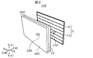
- FIG. 2 is an exploded perspective view illustrating an arrangement configuration of an example of main components in the illumination unit 110 of the illumination device 100 illustrated in FIG. 1.
- 3 is a light source unit
- 4 is a backlight unit
- 22 is a diffuser plate
- 202 is an optical sheet including the diffuser plate 22
- 203 is an exit surface
- 11 is a base chassis.
- the illumination device 100 includes a light source unit 3 and optical sheets 202.
- the diffusion plate 22 is composed of one or more sheets.
- the optical sheet 202 includes at least the diffusion plate 22, and is composed of the diffusion plate 22 and another optical sheet.
- the optical sheets other than the diffusion plate 22 of the optical sheets 202 are, for example, a vertical prism sheet, a horizontal prism sheet, and / or a brightness enhancement film.
- the main part which comprises the illumination part 110 of the illuminating device 100 is the light source part 3 for irradiating light from the Z direction back surface of the output surface 203.
- the light emitted from the light source unit 3 travels as indicated by an arrow 210, and is emitted as indicated by an arrow 220 through the diffusion plate 22, the optical sheets 202, and the like.
- the illumination unit 110 in FIG. 2 is a backlight device
- a liquid crystal panel is attached to the front surface in the Z direction of the emission surface 203, and a flat display device such as a liquid crystal display device is obtained.
- a video signal is supplied to the liquid crystal panel from a driving unit (not shown), and the light transmittance of the liquid crystal elements constituting each pixel is controlled based on the video signal.
- the light incident on the liquid crystal panel according to the arrow 220 is spatially modulated for each pixel of the liquid crystal panel, and an optical image formed by the modulation appears in the emitted light 220 and is displayed as an image. That is, the light incident on the liquid crystal panel is emitted as image light in the direction of the arrow 230.
- the arrows 210 and 220 are in the same direction as the Z direction (front) side.
- the backlight unit 4 is composed of one or a plurality of backlight blocks.
- the light source unit 3 includes a backlight unit including one or a plurality of backlight blocks, and the entire light source unit 3 is attached to and held by the base chassis 11.
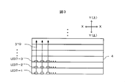
- FIG. 3 is a schematic diagram illustrating an example of the arrangement of a plurality of LEDs 7 that are light sources and the light emission direction of the light source unit 3 of the illumination device of the present invention.
- FIG. 3 is a perspective view when a part of the backlight unit 4 constituting the light source unit 3 is viewed from the emission surface 203 side.
- a plurality of LED groups 7-1 are arranged at equal intervals d in parallel with the X direction in which the light emission direction of the LEDs is directed upward in the Y direction (the direction of arrow 310).
- LED groups 7-2, 7-3,... are arranged. These LED groups 7-1, 7-2, 7-3,...
- the LED 7 emits (emits) white light here, but may be configured by a set of three LEDs that individually emit RGB three primary colors.
- FIG. 4A is a cross-sectional view for explaining an embodiment of the illumination device of the present invention.
- 7 is an LED
- 19 is a reflection sheet provided on the base chassis side
- 22 and 23 are diffusion plates
- 202 is an optical sheet including the diffusion plates 22 and 23
- 824 is a printed pattern formed on the diffusion plate 22 for dimming.
- 61 is emitted directly from the LED 7 and emitted directly toward the front surface of the diffuser plate 22
- 62 is reflected light emitted from the LED and reflected by the reflection sheet 19 and then emitted toward the front surface of the diffuser plate 22
- 63 is printed.
- Scattered light emitted toward the front surface of the diffusion plate 22 with the pattern 824 as a secondary light emitting surface, 24 is an air layer, and 62-1 and 63-1 are partial regions of the reflection sheet 19.
- the light from the LED 7 is emitted from the diffusion plate 22 while being reflected and diffused in the space (air layer 24 or the like) between the diffusion plate 22 and the reflection sheet 19 and propagated in the Y direction (upward). Thereby, the light reaches the tip of the backlight unit 4 in the Y direction, and the light emitted from the diffusion plate 22 is made uniform.
- FIG. 4B is a diagram for describing an embodiment of the illumination device of the present invention, and is a diagram illustrating an embodiment of the dimming pattern of the present invention that reduces the occurrence of uneven brightness in FIG. 4A.
- the broken line circle 67 is a diagram for explaining the aperture ratio when the dimming pattern is divided into unit tiles of a predetermined area, and 68 is a print pattern when the aperture ratio is gradually increased from 0% to 100%. It is.
- the dimming pattern 68 shown on the lower side of FIG. 4B forms, for example, the print pattern 824 of FIG. 4A for dimming.
- the dimming pattern 68 is divided into areas (unit tiles) having a predetermined area (size), and each of the divided areas has a predetermined aperture ratio (described later). That is, the dimming pattern 68 includes a plurality of areas (unit tiles) having a predetermined area having a predetermined aperture ratio.
- the light emitted from the LED 7 can be broadly classified into three types of components: direct light 61, reflected light 62, and scattered light 63.
- the direct light 61 is light that is emitted obliquely upward (on the emission surface 203 side in FIG. 2) from the emission port of the LED 7.
- the light emitted from the emission port of the LED 7 directly enters the diffusion plate 22, passes through the diffusion plate 22, and travels toward the emission surface 203 side of FIG. 2 (see the dotted line path).
- the ratio of the direct light 61 to the total amount of light emitted from the LED 7 is the smallest.
- the scattered light 63 is light that is emitted obliquely upward from the exit of the LED 7, and is directly incident on the lower surface of the diffusion plate 22, and after passing through the lower surface (incident surface) of the diffusion plate 22 or the diffusion plate 22, the diffusion plate 22. Reflected on the upper surface (exit surface). Thereafter, it goes downward from the lower surface of the diffusion plate 22 directly or again through the diffusion plate 22. Then, after passing through the air layer 24 and reflected by the reflection sheet 19 in the vicinity of the region 63-1 indicated by the elliptical shape, the light enters the air layer 24 and the diffusion plate 22, and enters the exit surface 203 side of FIG. Head (see dashed path).
- the scattered light 63 is amplified 2.5 times and is emitted to the emission surface 203 side.
- the ratio of the scattered light 63 to the total amount of light emitted from the LED 7 is the largest.
- the luminance value gradually increases (brighter) toward the center of the circle, and the luminance value gradually decreases (darker) toward the outside.
- the reflected light 62 travels downward from the exit of the LED 7, is reflected by the reflective sheet 19 near the region 62-1, enters the air layer 24 and the diffusion plate 22, and travels toward the exit surface 203 in FIG. 2. (See solid line path.)
- the ratio of the scattered light 62 to the total amount of light emitted from the LED 7 is less than the scattered light 63 and more than the direct light 61.
- the brightness value gradually increases (brighter) as the center of the circle becomes, and the brightness value gradually decreases (darker) as it goes outward.
- the direct light 61, the reflected light 62, and the scattered light 63 concentrate locally, a hot spot arises, This causes uneven brightness in the illumination device and the backlight device.
- partial displacement between the optical sheets 202 and the light source unit 3 and differences in arrangement of components in the light source unit 3 cause uneven brightness in the illumination device and the backlight device.
- a printing pattern 824 as shown in FIG. 4B is provided on the upper surface side of the diffusion plate 22 in order to reduce luminance unevenness caused by such hot spots.
- FIG. 4B is a view of the diffusion plate 22 viewed from the front side in the Z direction with respect to the peripheral portion of one LED 7.
- the print pattern 824 according to the present embodiment is made of, for example, white ink, and the ink is applied to the upper surface side of the diffusion plate 22 using a print mask created based on the light control pattern (see, for example, FIG. 4B). (Print).
- the print pattern 824 is formed on the upper surface side of the diffusion plate 22.
- a pattern at the time of designing a printing mask is referred to as a dimming pattern
- a pattern formed on the post-printing illumination device or the backlight device is referred to as a printing pattern.
- the ink used for the print pattern 824 is not limited to white, but may be, for example, black ink or blue ink mixed in white ink.
- the portion where the print pattern is formed is shown in black, and the portion where there is no print pattern is shown in white.
- the dimming pattern 68 is created in the entire position corresponding to the position immediately above the LED 7 and the light emitting side of the LED 7.
- the light control pattern 68 has a pattern density that decreases in the light emission direction of the LED 7 (from the left to the right of the paper). That is, the density of the dimming pattern is adjusted so that the density of the print pattern 824 is the highest in the vicinity of the portion where the hot spot occurs, that is, in the bright portion. Further, since the brightness of light from the diffusion plate 22 decreases as the distance from the vicinity of the portion where the hot spot is generated, the density of the dimming pattern is adjusted so that the density of the print pattern 824 decreases as the brightness decreases.
- aperture ratio is defined as the ratio of the print pattern (light control pattern) per unit area (referred to herein as “unit tile”). That is, when a print pattern is formed on the entire unit tile, the aperture ratio is 0%. When there is no print pattern at all for one unit tile, the aperture ratio is 100%.
- the broken line 67 shows unit tiles when the aperture ratio is divided into 64 stages, with the aperture ratio being 0% (# 1) to the aperture ratio being 100% (# 64). These 64 types of unit tiles are combined to form a print pattern 68 as shown on the lower side (below the dashed circle 67) in FIG. 4B.
- a plurality of unit tiles having an aperture ratio of 0% (# 1) are arranged immediately above the LED 7 and at a position corresponding to the light emission side of the LED 7, and the aperture ratio is 1 along the light emission direction of the LED 7 from there.
- Unit tiles having .56% (# 2), aperture ratio of 3.12% (# 3)..., Aperture ratio of 100% (# 64) are sequentially arranged.
- FIG. 4B the boundary of the unit tile is illustrated, but the unit tile represents a virtual region to the last, and actually, the unit tile or the boundary of the unit tile does not appear on the diffusion plate 22.
- the printed pattern 824 is a pattern for reducing the light intensity of the hot spot by blocking or reducing the light traveling from the diffusion plate 22 in the Z direction (forward direction) by reflection or absorption. Therefore, in FIG. 4A, it demonstrated as having formed the light control pattern by printing.
- the dimming pattern forming means is not limited to screen printing such as silk printing. For example, pattern formation by ink jet printing or the like may be used.
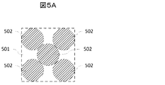
- FIG. 5A is a diagram illustrating an example of a dimming pattern for each conventional unit tile.
- FIG. 5B is a diagram illustrating an example of a case where printing variation occurs when printing is performed using the light control pattern of FIG. 5A.
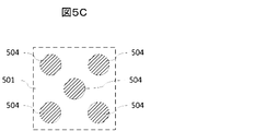
- FIG. 5C is a diagram showing an embodiment of a dimming pattern for each unit tile according to the present invention.
- FIG. 5D is a diagram illustrating an example of a print pattern when printing variation occurs when printing is performed using the mask of FIG. 5C.
- Reference numeral 501 denotes a unit tile area
- 502 and 504 are print figures when a print mask is designed
- 503 and 505 are print figures when a printing variation occurs after printing.
- the unit tile area 501 in FIG. 5C when the print mask is designed, printing is performed so that the printed figures do not overlap after printing even if there is printing variation.
- An interval (space) is provided in the figure 504.
- the interval between the printed figures 504 is about 100 ⁇ m.
- the printed figures 505 do not overlap each other and the thickness of the printed pattern does not change.
- the space in this specification is a printed figure with an aperture ratio of 100%.
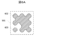
- FIG. 6A shows an example of a dimming pattern (print pattern) for each unit tile according to the second embodiment of the present invention when the aperture ratio of the dimming pattern in the region 501 of the unit tile is less than 50%. It is a figure which shows an example.
- 6B and 6C show the dimming pattern (printing pattern) for each unit tile according to the second embodiment of the present invention when the aperture ratio of the dimming pattern in the unit tile area 501 is less than 50%. It is a figure which shows one Example.
- the printed pattern 824 is formed on the upper surface of the diffusion plate 22 as in the embodiment of FIG. 4A. However, as described in the first embodiment, it may be on the lower surface of the diffusion plate 22 or on both surfaces. Further, the diffusion plate is not limited to the diffusion plate 22, and may be a diffusion plate at any position, may be formed on an optical sheet, or a combination thereof.
- the printed pattern 824 is a pattern for reducing the light intensity of the hot spot by blocking or reducing the light traveling from the diffusion plate 22 in the Z direction (forward direction) by reflection or absorption.
- the dimming pattern forming means is not limited to screen printing such as silk printing. For example, pattern formation by ink jet printing or the like may be used.
- one printed graphic is provided in the unit tile area 501 and a space is provided in the printed graphic.
- This one printed figure means that the number of labels is 1 when the unit tile area 501 of this printed figure is labeled by image processing. In FIG. 6A, the number of labels is 2, and in FIGS. 6B and 6C, the number of labels is 1. For example, as shown in FIG.
- the spaces 621 and 622 are round.
- the present invention is not particularly limited to the shape of the space. It may be an asymmetrical shape, an elliptical shape, or a figure with a predetermined shape such as a polygon or a multi-curve.
- the predetermined shape has the same area.
- FIG. 7 is a diagram illustrating an example of a dimming pattern for each unit tile according to the third embodiment of the present invention.
- a pattern formation prohibition area is provided near the boundary of each area 501 so that the printed figures or dimming patterns of the unit tile areas 501 do not overlap.
- a pattern formation prohibition area (print prohibition area) 731 is provided in the vicinity of the boundary between the two unit tiles. Space was secured.
- the width of the print prohibition area 731 is preferably about 50 ⁇ m in the normal screen printing inward from the boundaries of the unit tile areas 701-1 and 701-2. This width is approximately one half of the fluctuation width of the printed figure due to printing variations.
- the unit tiles according to the dimming patterns 602, 603, and 603 The printed figures in the region do not overlap each other after printing, and the thickness of the printed pattern does not change. According to this light control pattern, the density and shape of the print pattern hardly change, and a print pattern with a desired transmission amount can be formed. Therefore, the luminance unevenness can be reduced.
- the pattern formation prohibited area is an area having an aperture ratio of 100% in the same meaning as a space.
- the print pattern is formed on the upper surface of the diffusion plate 22 as in the embodiment of FIG. 4A.
- the lower surface of the diffusion plate 22 may be provided or may be provided on both sides.
- the diffusion plate is not limited to the diffusion plate 22, and may be a diffusion plate at any position, may be formed on an optical sheet, or a combination thereof.
- this printing pattern is a pattern for reducing the light intensity of the hot spot by blocking or reducing the light directed from the diffusion plate 22 in the Z direction (forward direction) by reflection or absorption.
- the dimming pattern forming means is not limited to screen printing such as silk printing. For example, pattern formation by ink jet printing or the like may be used.
- FIG. 8 is a diagram illustrating an example of a dimming pattern for each unit tile according to the fourth embodiment of the present invention.
- FIG. 8 shows unit tile areas 801-1, 801-2, 801-3, 801-4, 801-5, 801-6, 801-7 so that printed figures or dimming patterns do not overlap.
- (1) When there are unit tiles with an opening ratio of the adjacent unit tile area of 0%, the printed figures in the adjacent areas 801-1 to 801-3, 801-5 and 801-6 are joined.
- the pattern formation prohibition area is provided in the outline boundary portion (inside the adjacent boundary) of the areas 801-3 and 801-6 adjacent to the area 801-4 and 801-7 of the unit tile protecting the pattern formation prohibition area. 833-1 and 831-2 are provided.
- the width of the print prohibition area is the same as that in the third embodiment.
- the print area of each of the adjacent printed regions 801-1 to 801-7 is large, at least one of the above (1) and (2) is applied.
- the printed figures 802, 602, and 603 in the unit tile areas do not overlap each other even if there are variations during printing.
- the thickness of the printed pattern does not change.
- the printed pattern with a desired transmission amount can be formed with almost no change in the shade and shape of the printed pattern between printed figures in the same region and between adjacent unit tiles. Therefore, the luminance unevenness can be reduced.
- the print pattern is formed on the upper surface of the diffusion plate 22 as in the embodiment of FIG. 4A.
- the lower surface of the diffusion plate 22 may be provided or may be provided on both sides.
- the diffusion plate is not limited to the diffusion plate 22, and may be a diffusion plate at any position, may be formed on an optical sheet, or a combination thereof.
- this printing pattern is a pattern for reducing the light intensity of the hot spot by blocking or reducing the light directed from the diffusion plate 22 in the Z direction (forward direction) by reflection or absorption.
- the dimming pattern forming means is not limited to screen printing such as silk printing. For example, pattern formation by ink jet printing or the like may be used.
- the print pattern 824 is formed on the upper surface of the diffusion plate 22.
- the print pattern 824 may be formed on the lower surface of the diffusion plate 22 or may be formed on both surfaces of the diffusion plate 22.
- the print pattern 824 may be formed on any of the optical sheets 202, or may be formed on a plurality of optical sheets.
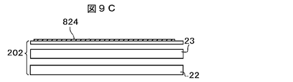
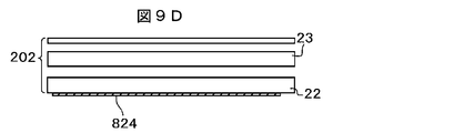
- 9A, 9B, 9C, 9D, and 9E are configurations of the optical sheet 202 of the embodiment of the illumination device and the backlight device according to the present invention, in which the print pattern 824 is formed on the optical sheet 202, respectively.
- 9A, 9B, 9C, 9D, and 9E show a print pattern 824 that forms unit tiles having an aperture ratio of 0% to 100%.
- 9A has the same configuration as FIG. 4A, and a printing pattern 824 is formed on the upper surface of the diffusion plate 22.
- a print pattern 824 is formed on the upper surface of the diffusion plate 23.
- a printing pattern 824 is formed on the upper surface of an optical sheet different from the diffusion plate.
- FIG. 9D a print pattern 824 is formed on the lower surface of the diffusion plate 22.
- print patterns 824 are formed on the upper and lower surfaces of all of the optical sheets 202. As described above, any optical sheet can form a printed pattern that can reduce luminance unevenness, and thus the degree of freedom in design and assembly is increased.
- the print pattern 824 of the present invention is formed on optical sheets.
- the present invention may be applied to a shielding or transmission pattern provided on another surface according to the design concept of the dimming pattern of the present invention.
- 10A and 10B are cross-sectional views for explaining an embodiment of the illumination device and the backlight device of the present invention.
- 10A and 10B show a configuration in which an LED cover 8 is added to the LED 7 as compared to the configuration in FIG. 4A.
- 10A and 10B illustrate an LED substrate 6 on which the LEDs 7 are mounted and a base chassis 11 that constitutes the light source unit 3 with respect to the configuration of FIG. 4A.
- the configuration other than the LED cover 8 is the same except that it is not shown.
- the LED 7 is surrounded by the LED substrate 6 and the LED cover 8 on which the LED 7 is mounted, and is configured such that light does not leak except at the emission port (near the root of the arrow 310).
- the print pattern 824 is formed on the upper surface of the LED cover 8.
- the configuration of the dimming pattern of the present invention can be applied to a print pattern formed on a component surface through which light emitted from a light source such as the LED 7 is transmitted, other than the optical sheets 202.
- FIG. 10B by applying the configuration of the dimming pattern of the present invention to the optical sheets 202 (in the example of FIG. 10B, the diffusion plate 22), a print pattern 824 is formed.
- 7 is an LED
- 19 is a reflection sheet provided on the base chassis side
- 22 and 23 are diffusion plates
- 202 is an optical sheet including the diffusion plates 22 and 23
- 824 is formed on the diffusion plate 22 for dimming.
- the white printed pattern 61 is a direct light emitted from the LED 7 and emitted toward the front surface of the diffusion plate 22
- 62 is a reflection emitted from the LED and reflected by the reflection sheet 19 and then emitted toward the front surface of the diffusion plate 22.
- 62-1 and 63-1 are partial regions of the reflection sheet 19.
- the light from the LED 7 is emitted from the diffusion plate 22 while being reflected and diffused in the space (air layer 24 or the like) between the diffusion plate 22 and the reflection sheet 19 and propagated in the Y direction (upward). Thereby, the light reaches the tip of the backlight unit 4 in the Y direction, and the light emitted from the diffusion plate 22 is made uniform.
- the first to sixth embodiments described above it is possible to realize an illuminating device and a backlight device that are configured with a printing pattern that does not have a problem of overlapping printed figures due to manufacturing variations such as printing.
- This printed pattern is to block or transmit light emitted from a light source such as an LED, and reduce luminance unevenness of light emitted from the emission surface of the illumination device or the backlight device. Accordingly, since the printed pattern can be formed as designed according to the first to sixth embodiments, the light emitted from the light source such as the LED is blocked or transmitted, and the light emitted from the emission surface of the illumination device or the backlight device. Brightness unevenness can be reduced. Therefore, according to the present embodiment, a high-luminance and high-quality illumination device and backlight device can be realized.
- the LED is used as the light source, but a discharge tube such as a cold cathode fluorescent lamp may be used.
- the air layer is used as the light propagation medium of the light source unit.
- a light guide plate may be used.
- the side view type illumination device and the backlight device have been described. However, a top view type illumination device and a backlight device may be used.
- the lighting device and the backlight device of the present invention are display panels whose colors and characters change at a predetermined cycle, such as traffic signs at intersections, road signs such as railway crossing indicator lights, and advertisement panels and signboards in stores. Can also be used. It can also be used as a lighting device for indoor lighting or outdoor lighting.
Landscapes
- Physics & Mathematics (AREA)
- General Physics & Mathematics (AREA)
- Optics & Photonics (AREA)
- Nonlinear Science (AREA)
- Mathematical Physics (AREA)
- Chemical & Material Sciences (AREA)
- Crystallography & Structural Chemistry (AREA)
- Planar Illumination Modules (AREA)
- Illuminated Signs And Luminous Advertising (AREA)
Abstract
本発明は、光源部と光学シートから成る出射面から光を照射するための照明装置において、前記光源部は、複数の光源を備え、前記光学シートは、1または2以上で構成され、かつ少なくとも拡散板を含み、前記光学シートの1または2以上は、前記光源から出射する光を遮蔽若しくは減光するための印刷パターンを有し、前記印刷パターンは、所定の調光パターンによって形成され、前記調光パターンは、それぞれ所定の開口率を具備する複数の単位タイルの領域に分割され、前記単位タイル毎に設けた印刷図形同志に所定のスペースを設けたことを特徴とする照明装置及びバックライト装置である。
Description
本発明は、エリアライトや室内照明等の照明装置、及び平面型のバックライト装置に係り、特に、複数の光源から出射した光から構成される出射光を面全体に均一化する照明装置及びバックライト装置に関する。
液晶表示装置は、液晶自身では発光しないので、液晶表示パネルの背面にバックライト装置を配置している。テレビジョン表示装置等、液晶表示装置に使用するバックライト装置では、光源として蛍光管や、LED(Light Emitting Diode)等の固体照明素子が使用されてきた。
また、上記バックライト装置は、その構造上、薄型化に適しているため、エリアライト等の薄型の照明装置としても使用される。
また、上記バックライト装置は、その構造上、薄型化に適しているため、エリアライト等の薄型の照明装置としても使用される。
上述の照明装置及びバックライト装置は、ひとつ若しくは複数の光源を有し、広範囲の平面上に配置するため、出射光に分布が生じて照明光のむらが発生する。
そのため、光学シートなどの構成部材に、照明光の輝度分布に応じてインクを塗布して透過量を制御する調光パターンを形成し、照明光の均一化を図っている。
そのため、光学シートなどの構成部材に、照明光の輝度分布に応じてインクを塗布して透過量を制御する調光パターンを形成し、照明光の均一化を図っている。
上述の調光パターンは、パターンの濃淡や有無で照明光の透過量を制御することによって、照明光の均一化を図るものである。しかし、スクリーン印刷やインクジェット印刷等でパターン形成する場合には、温度、湿度等の環境条件でパターン間の間隔の変動や印刷量の増減が発生する。このため、印刷面積が変動する(後述の図5A及び図5Bを参照。)。また、パターン形成するために複数回の印刷を行う場合には、さらに、印刷面積が変動し、パターン同士が重なり、さらには、パターンの厚み(濃淡)がばらつく。
以上のように、印刷ばらつきによってパターンの形状や濃淡が変わってしまうので、所望の透過量にすることができない。
特許文献1には、拡散プレートの下面に、照明光の均一化のための調光パターンをスクリーン印刷等で形成する技術が開示されている。特許文献1の調光パターンは、大径の第1調光ドット群から成る第1領域と、小径の第2調光ドット群から成る第2領域で構成され、照明光の入射光量が大きい第1領域からの照明光の透過量と、照明光の入射光量が小さい第2領域からの照明光の透過量とを調整して、照明光の均一化を図っている。
しかし、特許文献1では、印刷ばらつきによる印刷パターンの透過量の変動については、何ら言及していない。
本発明の目的は、上記のような問題に鑑み、印刷ばらつきがあっても、照明光の透過量の変動が小さい印刷パターンを形成する調光パターンによって、輝度むらの少ない照明装置及びバックライト装置を提供することにある。
以上のように、印刷ばらつきによってパターンの形状や濃淡が変わってしまうので、所望の透過量にすることができない。
特許文献1には、拡散プレートの下面に、照明光の均一化のための調光パターンをスクリーン印刷等で形成する技術が開示されている。特許文献1の調光パターンは、大径の第1調光ドット群から成る第1領域と、小径の第2調光ドット群から成る第2領域で構成され、照明光の入射光量が大きい第1領域からの照明光の透過量と、照明光の入射光量が小さい第2領域からの照明光の透過量とを調整して、照明光の均一化を図っている。
しかし、特許文献1では、印刷ばらつきによる印刷パターンの透過量の変動については、何ら言及していない。
本発明の目的は、上記のような問題に鑑み、印刷ばらつきがあっても、照明光の透過量の変動が小さい印刷パターンを形成する調光パターンによって、輝度むらの少ない照明装置及びバックライト装置を提供することにある。
上記の目的を達成するために、本発明の照明装置及びバックライト装置は、調光パターンを所定の面積及び形状の複数のエリア(単位タイル)に分割し、
(1)前記エリアそれぞれの縁には所定の幅の印刷禁止領域を設ける。
(2)前記エリアそれぞれについて、印刷面積が50%を超えるところからは、中抜きの印刷図形を設ける。
(1)前記エリアそれぞれの縁には所定の幅の印刷禁止領域を設ける。
(2)前記エリアそれぞれについて、印刷面積が50%を超えるところからは、中抜きの印刷図形を設ける。
即ち、本発明の照明装置及びバックライト装置は、光源部と光学シートを有し、光を照射するための照明装置において、前記光源部は、複数の光源を備え、前記光学シートは、1または2以上で構成され、かつ少なくとも拡散板を含み、前記光学シートの1または2以上は、前記光源から出射する光を遮蔽若しくは減光するための印刷パターンを有し、前記印刷パターンは、所定の調光パターンによって形成され、前記調光パターンは、それぞれ所定の開口率を具備する複数の単位タイルの領域に分割され、前記単位タイル毎に設けた印刷図形同士に所定のスペースを設けたことを本発明の第1の特徴とする。
上記本発明の第1の特徴の照明装置及びバックライト装置は、前記調光パターンは、さらに、前記単位タイルの領域のには、1つの印刷図形であって、当該印刷図形の中に所定の形状のスペースを設けて構成したことを本発明の第2の特徴とする。
上記本発明の第1の特徴または第2の特徴の照明装置及びバックライト装置は、前記調光パターンは、さらに、前記単位タイルの領域同士の境界付近に所定の幅のパターン形成禁止領域を設けたことを本発明の第3の特徴とする。
上記本発明の第1の特徴乃至第3の特徴のいずれかの特徴の照明装置及びバックライト装置は、開口率が0%の単位タイル同士が隣接する場合には、隣接する前記開口率が0%の単位タイル同士を接合した印刷図形としたことを本発明の第4の特徴とする。
本発明によれば、輝度むらの少ない照明装置及びバックライト装置を実現することができる。
以下に本発明の一実施形態を、図面等を用いて説明する。
なお、以下の説明は、本発明の一実施形態を説明するためのものであり、本発明の範囲を制限するものではない。従って、当業者であればこれらの各要素若しくは全要素をこれと均等なものに置換した実施形態を採用することが可能であり、これらの実施形態も本発明の範囲に含まれる。
また、本書では、各図の説明において、共通な機能を有する構成要素には同一の参照番号を付し、説明の重複をできるだけ避ける。
なお、以下の説明は、本発明の一実施形態を説明するためのものであり、本発明の範囲を制限するものではない。従って、当業者であればこれらの各要素若しくは全要素をこれと均等なものに置換した実施形態を採用することが可能であり、これらの実施形態も本発明の範囲に含まれる。
また、本書では、各図の説明において、共通な機能を有する構成要素には同一の参照番号を付し、説明の重複をできるだけ避ける。
まず、本実施形態の照明装置及びバックライト装置の全体構成について、図1~図5Dを参照しながらその概略を説明し、その後、本発明の課題を解決するための手段についての実施形態を説明する。
図1は、本発明の照明装置の一実施例の外観を示す斜視図である。100は照明装置、110は照明装置100の照明部である。
図1において、照明装置100は、照明部110にフレームや保護ガラスを設けたものである。また、説明を明確にするために、本明細書の図面において、Y方向は画面垂直方向(縦方向)を示し、X方向は画面水平方向(横方向)を示し、Z方向は奥行き方向(X方向及びY方向と直交する方向)を示す。
なお、照明装置は、バックライト装置としても良い。また、照明部110を照明装置またはバックライト装置として、平面型表示装置やその他の平面型表示パネルの一部としても良い。
図1において、照明装置100は、照明部110にフレームや保護ガラスを設けたものである。また、説明を明確にするために、本明細書の図面において、Y方向は画面垂直方向(縦方向)を示し、X方向は画面水平方向(横方向)を示し、Z方向は奥行き方向(X方向及びY方向と直交する方向)を示す。
なお、照明装置は、バックライト装置としても良い。また、照明部110を照明装置またはバックライト装置として、平面型表示装置やその他の平面型表示パネルの一部としても良い。
図2は、図1に示された照明装置100の照明部110における主要部品の一実施例の配置構成を示す分解斜視図である。3は光源部、4はバックライト部、22は拡散板、202は拡散板22を含む光学シート類、203は出射面、11はベースシャーシである。
照明装置100は、光源部3及び光学シート類202で構成される。また、拡散板22は、1枚乃至複数枚で構成される。さらに、光学シート類202は、少なくとも拡散板22を含んでおり、この拡散板22と、他の光学シートから構成される。光学シート類202の拡散板22以外の光学シートは、例えば、垂直プリズムシート、水平プリズムシート、及び/または輝度向上フィルム等である。
照明装置100は、光源部3及び光学シート類202で構成される。また、拡散板22は、1枚乃至複数枚で構成される。さらに、光学シート類202は、少なくとも拡散板22を含んでおり、この拡散板22と、他の光学シートから構成される。光学シート類202の拡散板22以外の光学シートは、例えば、垂直プリズムシート、水平プリズムシート、及び/または輝度向上フィルム等である。
図2において、照明装置100の照明部110を構成している主要部分は、出射面203のZ方向背面から光を照射するための光源部3である。ここで、光源部3から出た光は、矢印210のように進み、拡散板22、光学シート類202などを経て矢印220のように出射する。
図2の照明部110をバックライト装置とした場合には、出射面203のZ方向前面に液晶パネルが取り付けられ、液晶表示装置等の平面型表示装置となる。
その場合、液晶パネルには、図示しない駆動部から映像信号が供給され、当該映像信号に基づいて各画素を構成する液晶素子の光透過率が制御される。そして液晶パネルに矢印220に従って入射された光は液晶パネルの画素毎に空間的に変調され、当該変調によって形成された光学像が出射光220に現れ、画像として表示される。即ち、液晶パネルに入射した光は、矢印230の方向に画像光として出射する。言うまでもないが、矢印210及び220は、Z方向(前)側と同方向である。
その場合、液晶パネルには、図示しない駆動部から映像信号が供給され、当該映像信号に基づいて各画素を構成する液晶素子の光透過率が制御される。そして液晶パネルに矢印220に従って入射された光は液晶パネルの画素毎に空間的に変調され、当該変調によって形成された光学像が出射光220に現れ、画像として表示される。即ち、液晶パネルに入射した光は、矢印230の方向に画像光として出射する。言うまでもないが、矢印210及び220は、Z方向(前)側と同方向である。
バックライト部4は、1枚または複数枚のバックライトブロックで構成される。
なお、光源部3は、1枚または複数枚のバックライトブロックで構成されたバックライト部で構成され、さらに、光源部3全体は、ベースシャーシ11に取り付けられて保持される。
なお、光源部3は、1枚または複数枚のバックライトブロックで構成されたバックライト部で構成され、さらに、光源部3全体は、ベースシャーシ11に取り付けられて保持される。
図3は、本発明の照明装置の光源部3について、その光源である複数のLED7の配置と光の出射方向の一実施例を説明した模式図である。図3は、光源部3を構成するバックライト部4の一部を出射面203側から見た場合の斜視図である。
図3に示すように、LEDの光の出射方向がY方向の上(矢印310の方向)に向き、かつ、X方向に平行に複数のLED群7-1が均等な間隔dで並べて配置される。同様に、LED群7-2、7-3、・・・が配置される。また、これらLED群7-1、7-2、7-3、・・・同志は、Y方向に平行に均等な間隔pで下から上に並べて配置される。
なお、LED7の配置や光の出射方向については、図3では、下から上になるように構成したが、上から下、左から右、右から左、等、任意に配置して良い。またLED7は、ここでは白色光を放出(出射)するものとするが、RGBの三原色光を個々に放出する3つのLEDの組により構成してもよい。
図3に示すように、LEDの光の出射方向がY方向の上(矢印310の方向)に向き、かつ、X方向に平行に複数のLED群7-1が均等な間隔dで並べて配置される。同様に、LED群7-2、7-3、・・・が配置される。また、これらLED群7-1、7-2、7-3、・・・同志は、Y方向に平行に均等な間隔pで下から上に並べて配置される。
なお、LED7の配置や光の出射方向については、図3では、下から上になるように構成したが、上から下、左から右、右から左、等、任意に配置して良い。またLED7は、ここでは白色光を放出(出射)するものとするが、RGBの三原色光を個々に放出する3つのLEDの組により構成してもよい。
次に、図4Aと図4Bによって、輝度むらの発生の要因の1つとその対策について説明する。図4Aは、本発明の照明装置の一実施例を説明するための断面図である。7はLED、19はベースシャーシ側に設けた反射シート、22と23は拡散板、202は拡散板22及び23を含む光学シート類、824は調光用として拡散板22上に形成した印刷パターン、61はLED7から出射し、拡散板22の前面方向に出射する直射光、62はLEDから出射し、反射シート19で反射してから拡散板22の前面方向に出射する反射光、63は印刷パターン824を2次発光面として拡散板22の前面方向に出射する散乱光、24は空気層、62-1と63-1は反射シート19の一部の領域である。
LED7からの光は、拡散板22と反射シート19との間の空間(空気層24等)を反射、拡散しながら拡散板22から出射して、Y方向(上)に伝播される。これによって、バックライト部4のY方向先端にまで光を到達させて拡散板22から出射される光の均一化を図っている。
LED7からの光は、拡散板22と反射シート19との間の空間(空気層24等)を反射、拡散しながら拡散板22から出射して、Y方向(上)に伝播される。これによって、バックライト部4のY方向先端にまで光を到達させて拡散板22から出射される光の均一化を図っている。
また、図4Bは、本発明の照明装置の一実施例を説明するための図で、図4Aの輝度むらの発生を低減する本発明の調光パターンの一実施例について説明する図である。破線円67内は、調光パターンを所定の面積の単位タイルに分けた場合の、開口率を説明する図であり、68は開口率を0%から100%まで徐々に大きくした場合の印刷パターンである。
図4Bの下側に示す調光パターン68は、調光用として、例えば、図4Aの印刷パターン824を形成する。この調光パターン68は、所定の面積(サイズ)のエリア(単位タイル)毎に分割され、この分割された各エリアは、それぞれ所定の開口率(後述する)を有する。即ち、調光パターン68は、所定の開口率を有する所定の面積の、複数のエリア(単位タイル)で構成される。
図4Bの下側に示す調光パターン68は、調光用として、例えば、図4Aの印刷パターン824を形成する。この調光パターン68は、所定の面積(サイズ)のエリア(単位タイル)毎に分割され、この分割された各エリアは、それぞれ所定の開口率(後述する)を有する。即ち、調光パターン68は、所定の開口率を有する所定の面積の、複数のエリア(単位タイル)で構成される。
図4Aに示すように、LED7から出射した光は、大別して、直射光61、反射光62、及び散乱光63の3種類の成分に分類することができる。
直射光61は、LED7の出射口から斜め上方向(図2の出射面203側)に出射する光である。LED7の出射口から出射した光は、直接、拡散板22に入射し、拡散板22を通過し、図2の出射面203側に向かう(点線の経路を参照。)。LED7から出射する全光量に対して、この直射光61の占める割合は一番少ない。
散乱光63は、LED7の出射口から斜め上方向に出射する光であり、直接、拡散板22の下面に入射し、拡散板22下面(入射面)、あるいは拡散板22を通過後に拡散板22上面(出射面)で反射する。その後、拡散板22下面から直接的に、または再度拡散板22を通過して下方に向かう。そして、空気層24を通過して、楕円形状で示している領域63-1付近の反射シート19で反射してから、空気層24、拡散板22に入射し、図2の出射面203側に向かう(破線の経路を参照。)。この散乱光63は、2.5倍に増幅され出射面203側に出射する。LED7から出射する全光量に対して、この散乱光63の占める割合は一番多い。なお、領域63-1では、円の中心になるほど輝度値が徐々に高く(明るく)、外側になるほど輝度値が徐々に低く(暗く)なる。
反射光62は、LED7の出射口から、下方に向かい、領域62-1付近の反射シート19で反射してから、空気層24、拡散板22に入射し、図2の出射面203側に向かう(実線の経路を参照。)。LED7から出射する全光量に対して、この散乱光62の占める割合は、散乱光63より少なく直射光61より多い。なお、領域62-1では、円の中心になるほど輝度値が徐々に高く(明るく)、外側になるほど輝度値が徐々に低く(暗く)なる。
このように、拡散板22の、LED7の直上及びLED7の光出射側と対応する位置においては、直射光61、反射光62、及び散乱光63が局所的に集中するためにホットスポットが生じ、これが照明装置及びバックライト装置の輝度むらの原因となる。また、ホットスポットの他、光学シート類202と光源部3との部分的なずれや光源部3内の構成要素の配置の違いが、照明装置及びバックライト装置の輝度むらの原因となる。
直射光61は、LED7の出射口から斜め上方向(図2の出射面203側)に出射する光である。LED7の出射口から出射した光は、直接、拡散板22に入射し、拡散板22を通過し、図2の出射面203側に向かう(点線の経路を参照。)。LED7から出射する全光量に対して、この直射光61の占める割合は一番少ない。
散乱光63は、LED7の出射口から斜め上方向に出射する光であり、直接、拡散板22の下面に入射し、拡散板22下面(入射面)、あるいは拡散板22を通過後に拡散板22上面(出射面)で反射する。その後、拡散板22下面から直接的に、または再度拡散板22を通過して下方に向かう。そして、空気層24を通過して、楕円形状で示している領域63-1付近の反射シート19で反射してから、空気層24、拡散板22に入射し、図2の出射面203側に向かう(破線の経路を参照。)。この散乱光63は、2.5倍に増幅され出射面203側に出射する。LED7から出射する全光量に対して、この散乱光63の占める割合は一番多い。なお、領域63-1では、円の中心になるほど輝度値が徐々に高く(明るく)、外側になるほど輝度値が徐々に低く(暗く)なる。
反射光62は、LED7の出射口から、下方に向かい、領域62-1付近の反射シート19で反射してから、空気層24、拡散板22に入射し、図2の出射面203側に向かう(実線の経路を参照。)。LED7から出射する全光量に対して、この散乱光62の占める割合は、散乱光63より少なく直射光61より多い。なお、領域62-1では、円の中心になるほど輝度値が徐々に高く(明るく)、外側になるほど輝度値が徐々に低く(暗く)なる。
このように、拡散板22の、LED7の直上及びLED7の光出射側と対応する位置においては、直射光61、反射光62、及び散乱光63が局所的に集中するためにホットスポットが生じ、これが照明装置及びバックライト装置の輝度むらの原因となる。また、ホットスポットの他、光学シート類202と光源部3との部分的なずれや光源部3内の構成要素の配置の違いが、照明装置及びバックライト装置の輝度むらの原因となる。
かかるホットスポット等に起因する輝度むらを少なくするために、本実施例では、拡散板22の上面側に、図4Bに示すような印刷パターン824を設けている。図4Bは、1つのLED7の周辺部分について、拡散板22をZ方向の前側から見た図である。本実施例に係る印刷パターン824は、例えば白色のインクにより構成されており、調光パターン(例えば、図4B参照)に基づいて作成した印刷マスクによって、拡散板22の上面側にインクを塗布する(印刷する)。これにより、印刷パターン824を拡散板22の上面側に形成する。
なお、本明細書では、印刷マスク設計時のパターンを調光パターンと称し、印刷後照明装置またはバックライト装置に形成されたパターンを印刷パターンと称する。
なお、本明細書では、印刷マスク設計時のパターンを調光パターンと称し、印刷後照明装置またはバックライト装置に形成されたパターンを印刷パターンと称する。
この印刷パターン824によって、拡散板22からZ方向(前方向)に向かう光を反射または吸収により遮光または減光することができ、その結果、ホットスポット等による光の局所的な集中が低減し、輝度むらを少なくする。なお、印刷パターン824に使われるインクは白色のみではなく、例えば黒色インクや青色インクを白色インクに混入したものであっても良い。また、図4Bにおいては、印刷パターンを見易くする為に、印刷パターンが形成されている部分を黒色で、印刷パターンが無い部分を白色で示している。
即ち、本実施例に係る印刷パターン824を形成するための印刷マスクとして、LED7の直上及びLED7の光出射側と対応する位置の全体に、調光パターン68を作成する。この調光パターン68は、LED7の光出射方向(紙面の左から右側への方向)に向かうに従って、パターンの密度が低下させる。つまり、ホットスポットが生じる部分近傍、即ち、明るい部分については印刷パターン824の密度が最も高くなるように調光パターンの密度を調整する。また、ホットスポットが生じる部分近傍から離れるに従って拡散板22からの光の輝度が低下するので、この輝度低下に従って印刷パターン824の密度が低くなるように調光パターンの密度を調整する。
即ち、本実施例に係る印刷パターン824を形成するための印刷マスクとして、LED7の直上及びLED7の光出射側と対応する位置の全体に、調光パターン68を作成する。この調光パターン68は、LED7の光出射方向(紙面の左から右側への方向)に向かうに従って、パターンの密度が低下させる。つまり、ホットスポットが生じる部分近傍、即ち、明るい部分については印刷パターン824の密度が最も高くなるように調光パターンの密度を調整する。また、ホットスポットが生じる部分近傍から離れるに従って拡散板22からの光の輝度が低下するので、この輝度低下に従って印刷パターン824の密度が低くなるように調光パターンの密度を調整する。
上記調光パターンの密度をここでは「開口率」と称する。この開口率は、単位面積(ここでは「単位タイル」と称する)当たりの印刷パターン(調光パターン)の割合と定義する。つまり、1つの単位タイルの全体に印刷パターンを形成している場合には、その開口率は0%である。また、1つの単位タイルの全体に全く印刷パターンがない場合には、開口率は100%である。
図4Bでは、破線の円67内には、開口率が0%(#1)~開口率が100%(#64)と開口率を64段階に分けた場合の単位タイルについて示している。この64種類の単位タイルを組合せて、図4Bの下方(破線の円67の下)側に示すように印刷パターン68を形成する。例えば、LED7の直上及びLED7の光出射側と対応する位置には開口率が0%(#1)の単位タイルを複数個配列し、そこからLED7の光出射方向に沿って、開口率が1.56%(#2)、開口率が3.12%(#3)…開口率が100%(#64)の単位タイルを順次配列する。これによって、ホットスポットが生じる最も明るい部分では開口率が低く(0)、ホットスポットから離れるにつれて徐々に開口率が高くなる印刷パターン68を形成することができる。
なお、図4Bでは単位タイルの境界が図示されているが、単位タイルはあくまでも仮想的な領域を示すものであり、実際には単位タイルまたは単位タイルの境界は拡散板22上に現れない。
図4Bでは、破線の円67内には、開口率が0%(#1)~開口率が100%(#64)と開口率を64段階に分けた場合の単位タイルについて示している。この64種類の単位タイルを組合せて、図4Bの下方(破線の円67の下)側に示すように印刷パターン68を形成する。例えば、LED7の直上及びLED7の光出射側と対応する位置には開口率が0%(#1)の単位タイルを複数個配列し、そこからLED7の光出射方向に沿って、開口率が1.56%(#2)、開口率が3.12%(#3)…開口率が100%(#64)の単位タイルを順次配列する。これによって、ホットスポットが生じる最も明るい部分では開口率が低く(0)、ホットスポットから離れるにつれて徐々に開口率が高くなる印刷パターン68を形成することができる。
なお、図4Bでは単位タイルの境界が図示されているが、単位タイルはあくまでも仮想的な領域を示すものであり、実際には単位タイルまたは単位タイルの境界は拡散板22上に現れない。
なお、この印刷パターン824は、拡散板22からZ方向(前方向)に向かう光を反射または吸収により遮光または減光してホットスポットの光強度が低減するためのパターンである。従って、図4Aでは、調光パターンを印刷で形成したとして説明した。しかし、調光パターンの形成手段としては、シルク印刷等のスクリーン印刷に限らない。例えば、インクジェット印刷等によるパターン形成でも良い。
次に、図5A、図5B、図5C、及び図5Dを用いて、本発明の調光パターンの構成について説明する。図5Aは、従来の単位タイル毎の調光パターンの一例を示す図である。図5Bは、図5Aの調光パターンで印刷した場合に、印刷ばらつきが発生した場合の一例を示す図である。図5Cは、本発明の単位タイル毎の調光パターンの一実施例を示す図である。図5Dは、図5Cのマスクで印刷した場合に、印刷ばらつきが発生した場合の印刷パターンの一実施例を示す図である。501は単位タイルの領域、502と504は印刷マスク設計時の印刷図形、503と505は、印刷後に印刷ばらつきが発生した場合の印刷図形である。
図5Aの単位タイルの領域501に示すように、印刷マスクの設計時に、印刷図形502同士の間隔(スペース)を設けなかった場合には、図5Bの単位タイルの領域501に示すように、印刷時のばらつきによっては、印刷図形503の一部が互いに重なって、印刷パターンの厚みまで変わってしまう。この結果、パターンの濃淡や、パターンの形状が変わってしまうので、所望の透過量にすることができない。従って、輝度むらが大きい。
そこで、本発明の照明装置及びバックライト装置では、図5Cの単位タイルの領域501に示すように、印刷マスクの設計時に、印刷ばらつきがあっても印刷後に各印刷図形が重ならないように、印刷図形504に間隔(スペース)を設ける。例えば、通常のスクリーン印刷では、各印刷図形504の間隔は、100μm程度である。
その結果、図5Dの単位タイルの領域501に示すように、印刷時のばらつきがあっても、印刷図形505が互いに重ならず、印刷パターンの厚みは変わらない。この調光パターンによれば、印刷パターンの濃淡や形状がほとんど変わらず、所望の透過量の印刷パターンを形成することができる。従って、輝度むらを小さくすることができる。
なお、本明細書におけるスペースとは、開口率100%の印刷図形である。
その結果、図5Dの単位タイルの領域501に示すように、印刷時のばらつきがあっても、印刷図形505が互いに重ならず、印刷パターンの厚みは変わらない。この調光パターンによれば、印刷パターンの濃淡や形状がほとんど変わらず、所望の透過量の印刷パターンを形成することができる。従って、輝度むらを小さくすることができる。
なお、本明細書におけるスペースとは、開口率100%の印刷図形である。
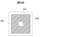
次に、図6A、図6B、及び図6Cを用いて、本発明の他の調光パターンについて説明する。図6Aは、単位タイルの領域501内の調光パターンの開口率が50%未満となった場合の、本発明の第2の実施形態の単位タイル毎の調光パターン(印刷パターン)の一実施例を示す図である。図6B及び図6Cは、単位タイルの領域501内の調光パターンの開口率が50%未満となった場合の、本発明の第2の実施形態の単位タイル毎の調光パターン(印刷パターン)の一実施例を示す図である。
なお、図6A-図6Cの実施例においても、図4Aの実施例と同様に印刷パターン824は拡散板22の上面に形成される。しかし、実施例1で述べたように、拡散板22の下面でも良く、また、両面にあっても良い。また、拡散板22に限らず、どの位置の拡散板でも良く、さらに、光学シート類に形成しても良く、それらの組合せでも良い。
また、この印刷パターン824は、拡散板22からZ方向(前方向)に向かう光を反射または吸収により遮光または減光してホットスポットの光強度が低減するためのパターンである。なお、調光パターンの形成手段としては、シルク印刷等のスクリーン印刷に限らない。例えば、インクジェット印刷等によるパターン形成でも良い。
また、この印刷パターン824は、拡散板22からZ方向(前方向)に向かう光を反射または吸収により遮光または減光してホットスポットの光強度が低減するためのパターンである。なお、調光パターンの形成手段としては、シルク印刷等のスクリーン印刷に限らない。例えば、インクジェット印刷等によるパターン形成でも良い。
図6Aに示すように、単位タイルの領域501内の調光パターンの開口率が50%未満である場合には、領域501内の各印刷図形602及び603にスペースを持たせることが難しくなる。即ち、開口率が小さくなるにつれて、印刷図形同志のパターンの重なりを防止することが困難になる。
そこで、本発明の第2の実施形態では、単位タイルの領域501内の印刷図形を1つにして、その印刷図形内にスペースを設けた。なお、この1つの印刷図形とは、この印刷図形の単位タイルの領域501を画像処理してラベル付けした場合に、ラベル数が1であることを意味する。また、図6Aでは、ラベル数は2であり、図6B及び図6Cでは、ラベル数は1である。
例えば、図6Bに示すように、単位タイルの領域501内に1つだけの印刷図形603を設け、この印刷図形603内に、円形のスペース621を設けた。また例えば、図6Cに示すように、単位タイルの領域501内に1つだけの印刷図形604を設け、この印刷図形604内に、2つの円形のスペース(開口率100%)622を設けた。
この結果、図6B及び図6Cの単位タイルの領域501の調光パターンから分かるように、印刷時のばらつきがあっても、印刷図形602、603が互いに重ならず、印刷パターンの厚みは変わらない。この調光パターンによれば、印刷パターンの濃淡や形状がほとんど変わらず、所望の透過量の印刷パターンを形成することができる。従って、輝度むらを小さくすることができる。
なお、図6A~図6Cの実施例では、スペース621及び622は正円形であった。しかし、本発明は、スペースの形状には特に限定されない。非対称形でも良く、楕円形でも良く、多角形や、多曲線で囲まれたような、所定の形状の図形で良い。
好ましくは、この所定の形状は、同一の面積を有する。
そこで、本発明の第2の実施形態では、単位タイルの領域501内の印刷図形を1つにして、その印刷図形内にスペースを設けた。なお、この1つの印刷図形とは、この印刷図形の単位タイルの領域501を画像処理してラベル付けした場合に、ラベル数が1であることを意味する。また、図6Aでは、ラベル数は2であり、図6B及び図6Cでは、ラベル数は1である。
例えば、図6Bに示すように、単位タイルの領域501内に1つだけの印刷図形603を設け、この印刷図形603内に、円形のスペース621を設けた。また例えば、図6Cに示すように、単位タイルの領域501内に1つだけの印刷図形604を設け、この印刷図形604内に、2つの円形のスペース(開口率100%)622を設けた。
この結果、図6B及び図6Cの単位タイルの領域501の調光パターンから分かるように、印刷時のばらつきがあっても、印刷図形602、603が互いに重ならず、印刷パターンの厚みは変わらない。この調光パターンによれば、印刷パターンの濃淡や形状がほとんど変わらず、所望の透過量の印刷パターンを形成することができる。従って、輝度むらを小さくすることができる。
なお、図6A~図6Cの実施例では、スペース621及び622は正円形であった。しかし、本発明は、スペースの形状には特に限定されない。非対称形でも良く、楕円形でも良く、多角形や、多曲線で囲まれたような、所定の形状の図形で良い。
好ましくは、この所定の形状は、同一の面積を有する。
次に、図7を用いて、本発明の別の調光パターンについて説明する。図7は、本発明の第3の実施形態の単位タイル毎の調光パターンの一実施例を示す図である。図7は、単位タイルの領域501同志の印刷図形若しくは調光パターンが重ならないように、各領域501の境界付近にパターン形成禁止領域を設けたものである。
即ち、図7に示すように、2つの単位タイルの領域701-1と702-1において、どちらもその境界付近にパターン形成禁止領域(印刷禁止エリア)731を設け、隣接する単位タイル同士とのスペースを確保した。
印刷禁止エリア731の幅は、好ましくは、各単位タイルの領域701-1や701-2の境界から内側に、通常のスクリーン印刷では、50μm程度である。この幅は、印刷ばらつきによる印刷図形の変動幅の略2分の1である。
この結果、図7の調光パターン(単位タイルの領域701-1及び701-2)から分かるように、印刷時のばらつきがあっても、調光パターン602、603、及び603による各単位タイルの領域内の印刷図形が、印刷後に、互いに重ならず、印刷パターンの厚みは変わらない。この調光パターンによれば、印刷パターンの濃淡や形状がほとんど変わらず、所望の透過量の印刷パターンを形成することができる。従って、輝度むらを小さくすることができる。なお、パターン形成禁止領域とは、スペースと同様の意味で、開口率が100%の領域である。
印刷禁止エリア731の幅は、好ましくは、各単位タイルの領域701-1や701-2の境界から内側に、通常のスクリーン印刷では、50μm程度である。この幅は、印刷ばらつきによる印刷図形の変動幅の略2分の1である。
この結果、図7の調光パターン(単位タイルの領域701-1及び701-2)から分かるように、印刷時のばらつきがあっても、調光パターン602、603、及び603による各単位タイルの領域内の印刷図形が、印刷後に、互いに重ならず、印刷パターンの厚みは変わらない。この調光パターンによれば、印刷パターンの濃淡や形状がほとんど変わらず、所望の透過量の印刷パターンを形成することができる。従って、輝度むらを小さくすることができる。なお、パターン形成禁止領域とは、スペースと同様の意味で、開口率が100%の領域である。
なお、図7の実施例においても、図4Aの実施例と同様に印刷パターンは拡散板22の上面に形成される。しかし、実施例1及び実施例2で述べたように、拡散板22の下面でも良く、また、両面にあっても良い。また、拡散板22に限らず、どの位置の拡散板でも良く、さらに、光学シート類に形成しても良く、それらの組合せでも良い。
また、この印刷パターンは、拡散板22からZ方向(前方向)に向かう光を反射または吸収により遮光または減光してホットスポットの光強度が低減するためのパターンである。なお、調光パターンの形成手段としては、シルク印刷等のスクリーン印刷に限らない。例えば、インクジェット印刷等によるパターン形成でも良い。
また、この印刷パターンは、拡散板22からZ方向(前方向)に向かう光を反射または吸収により遮光または減光してホットスポットの光強度が低減するためのパターンである。なお、調光パターンの形成手段としては、シルク印刷等のスクリーン印刷に限らない。例えば、インクジェット印刷等によるパターン形成でも良い。
次に、図8を用いて、本発明の別の調光パターンについて説明する。図8は、本発明の第4の実施形態の単位タイル毎の調光パターンの一実施例を示す図である。図8は、単位タイルの領域801-1、801-2、801-3、801-4、801-5、801-6、801-7同志の印刷図形若しくは調光パターンが重ならないように、
(1)隣接する単位タイルの領域の開口率が0%の単位タイル同志があった場合には、隣接する領域801-1~801-3、801-5及び801-6の印刷図形を接合して1つの印刷図形802とする。
(2)パターン形成禁止領域を守る単位タイルの領域801-4及び801-7と隣接する領域801-3及び801-6の概要する境界部分(隣接する境界の内側)には、パターン形成禁止領域831-1及び831-2を設けたものである。印刷禁止エリアの幅は、実施例3と同様である。
(1)隣接する単位タイルの領域の開口率が0%の単位タイル同志があった場合には、隣接する領域801-1~801-3、801-5及び801-6の印刷図形を接合して1つの印刷図形802とする。
(2)パターン形成禁止領域を守る単位タイルの領域801-4及び801-7と隣接する領域801-3及び801-6の概要する境界部分(隣接する境界の内側)には、パターン形成禁止領域831-1及び831-2を設けたものである。印刷禁止エリアの幅は、実施例3と同様である。
このように、隣接する領域801-1~801-7それぞれの印刷図形の領域の印刷面積が大である場合には、上記(1)または(2)の少なくともいずれか1つを適用する。
この結果、図8の単位タイルの領域801-1~801-7に示すように、印刷時のばらつきがあっても、各単位タイルの領域内の印刷図形802、602及び603が互いに重ならず、印刷パターンの厚みは変わらない。この調光パターンによれば、同一領域内の印刷図形同士、及び隣接する単位タイル同志でも、印刷パターンの濃淡や形状がほとんど変わらず、所望の透過量の印刷パターンを形成することができる。従って、輝度むらを小さくすることができる。
この結果、図8の単位タイルの領域801-1~801-7に示すように、印刷時のばらつきがあっても、各単位タイルの領域内の印刷図形802、602及び603が互いに重ならず、印刷パターンの厚みは変わらない。この調光パターンによれば、同一領域内の印刷図形同士、及び隣接する単位タイル同志でも、印刷パターンの濃淡や形状がほとんど変わらず、所望の透過量の印刷パターンを形成することができる。従って、輝度むらを小さくすることができる。
なお、図8の実施例においても、図4Aの実施例と同様に印刷パターンは拡散板22の上面に形成される。しかし、実施例1及び実施例2で述べたように、拡散板22の下面でも良く、また、両面にあっても良い。また、拡散板22に限らず、どの位置の拡散板でも良く、さらに、光学シート類に形成しても良く、それらの組合せでも良い。
また、この印刷パターンは、拡散板22からZ方向(前方向)に向かう光を反射または吸収により遮光または減光してホットスポットの光強度が低減するためのパターンである。なお、調光パターンの形成手段としては、シルク印刷等のスクリーン印刷に限らない。例えば、インクジェット印刷等によるパターン形成でも良い。
また、この印刷パターンは、拡散板22からZ方向(前方向)に向かう光を反射または吸収により遮光または減光してホットスポットの光強度が低減するためのパターンである。なお、調光パターンの形成手段としては、シルク印刷等のスクリーン印刷に限らない。例えば、インクジェット印刷等によるパターン形成でも良い。
上記実施例1~4における図4Aでは、印刷パターン824が拡散板22の上面に形成されている。しかし、印刷パターン824は、拡散板22の下面に形成されても良く、また、拡散板22の両面に形成されても良い。また、拡散板22に限らず、どの拡散板に形成されても良い。さらに、印刷パターン824を光学シート類202のいずれに形成しても良く、また、複数の光学シート類に形成されても良い。
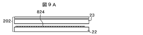
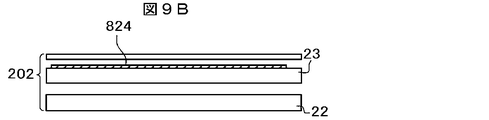
図9A、図9B、図9C、図9D及び図9Eは、それぞれ、印刷パターン824を光学シート類202に形成した、本発明の照明装置及びバックライト装置の一実施例の光学シート類202の構成を示す断面図である。
図9A、図9B、図9C、図9D及び図9Eは、それぞれ、印刷パターン824を光学シート類202に形成した、本発明の照明装置及びバックライト装置の一実施例の光学シート類202の構成を示す断面図である。
図9A、図9B、図9C、図9D及び図9Eは、開口率が0%~100%の単位タイルを形成している印刷パターン824を示している。
図9Aは、図4Aと同じ構成であり、拡散板22の上面に印刷パターン824が形成されている。
図9Bは、拡散板23の上面に印刷パターン824が形成されている。
図9Cは、拡散板と異なる光学シートの上面に印刷パターン824が形成されている。
図9Dは、拡散板22の下面に印刷パターン824が形成されている。
図9Eは、光学シート類202のすべての上下面に印刷パターン824が形成されている。
このように、光学シート類のいずれであっても、輝度むらを低減することができる印刷パターンを形成可能であるので、設計上及び組立上の自由度が高くなる。
図9Aは、図4Aと同じ構成であり、拡散板22の上面に印刷パターン824が形成されている。
図9Bは、拡散板23の上面に印刷パターン824が形成されている。
図9Cは、拡散板と異なる光学シートの上面に印刷パターン824が形成されている。
図9Dは、拡散板22の下面に印刷パターン824が形成されている。
図9Eは、光学シート類202のすべての上下面に印刷パターン824が形成されている。
このように、光学シート類のいずれであっても、輝度むらを低減することができる印刷パターンを形成可能であるので、設計上及び組立上の自由度が高くなる。
上記実施例1~5において、本発明の印刷パターン824は、光学シート類に形成されている。しかし、本実施例の図10A及び図10Bに示すように、本発明の調光パターンの設計思想によって、他の面に設けた遮蔽若しくは透過パターンに適用しても良い。
図10A及び図10Bは、本発明の照明装置及びバックライト装置の一実施例を説明するための断面図である。図10A及び図10Bは、図4Aの構成に比べて、LED7にLEDカバー8を追加した構成である。なお、図10A及び図10Bは、図4Aの構成に対して、LED7を搭載するLED基板6と光源部3を構成するベースシャーシ11を図示している。しかし、図4Aでは、図示していなかっただけで、LEDカバー8以外の構成は同じである。
図10A及び図10Bは、本発明の照明装置及びバックライト装置の一実施例を説明するための断面図である。図10A及び図10Bは、図4Aの構成に比べて、LED7にLEDカバー8を追加した構成である。なお、図10A及び図10Bは、図4Aの構成に対して、LED7を搭載するLED基板6と光源部3を構成するベースシャーシ11を図示している。しかし、図4Aでは、図示していなかっただけで、LEDカバー8以外の構成は同じである。
図10A及び図10Bにおいて、LED7は、LED7を搭載しているLED基板6とLEDカバー8に囲まれ、出射口(矢印310の根本付近)以外には光が漏れないような構成としている。しかし、多少透過する光があるため、LEDカバー8の上面に印刷パターン824を形成したものである。
このように、光学シート類202以外であっても、LED7等の光源から出射する光が透過する部品面に形成する印刷パターンに対して、本発明の調光パターンの構成が適用可能である。
さらに、図10Bに示すように、光学シート類202(図10Bの実施例では、拡散板22)にも、本発明の調光パターンの構成を適用して、印刷パターン824を形成することで、図10Aに比べて、さらに輝度むらを低減することができる。
加えて、7はLED、19はベースシャーシ側に設けた反射シート、22と23は拡散板、202は拡散板22及び23を含む光学シート類、824は調光用として拡散板22上に形成した白色の印刷パターン、61はLED7から出射し、拡散板22の前面方向に出射する直射光、62はLEDから出射し、反射シート19で反射してから拡散板22の前面方向に出射する反射光、63は印刷パターン824を2次発光面として拡散板22の前面方向に出射する散乱光、24は空気層、62-1と63-1は反射シート19の一部の領域である。
LED7からの光は、拡散板22と反射シート19との間の空間(空気層24等)を反射、拡散しながら拡散板22から出射して、Y方向(上)に伝播される。これによって、バックライト部4のY方向先端にまで光を到達させて拡散板22から出射される光の均一化を図っている。
このように、光学シート類202以外であっても、LED7等の光源から出射する光が透過する部品面に形成する印刷パターンに対して、本発明の調光パターンの構成が適用可能である。
さらに、図10Bに示すように、光学シート類202(図10Bの実施例では、拡散板22)にも、本発明の調光パターンの構成を適用して、印刷パターン824を形成することで、図10Aに比べて、さらに輝度むらを低減することができる。
加えて、7はLED、19はベースシャーシ側に設けた反射シート、22と23は拡散板、202は拡散板22及び23を含む光学シート類、824は調光用として拡散板22上に形成した白色の印刷パターン、61はLED7から出射し、拡散板22の前面方向に出射する直射光、62はLEDから出射し、反射シート19で反射してから拡散板22の前面方向に出射する反射光、63は印刷パターン824を2次発光面として拡散板22の前面方向に出射する散乱光、24は空気層、62-1と63-1は反射シート19の一部の領域である。
LED7からの光は、拡散板22と反射シート19との間の空間(空気層24等)を反射、拡散しながら拡散板22から出射して、Y方向(上)に伝播される。これによって、バックライト部4のY方向先端にまで光を到達させて拡散板22から出射される光の均一化を図っている。
上述の実施例1~実施例6によれば、印刷等の製造上のばらつきによって、それぞれの印刷図形が重なる不具合がない印刷パターンで構成された照明装置及びバックライト装置を実現できる。
この印刷パターンは、LED等の光源から出射する光を、遮光または透過させ、照明装置またはバックライト装置の出射面から出射する光の輝度むらを低減するものである。
従って、実施例1~実施例6によって、印刷パターンが、設計通りに形成できるので、LED等の光源から出射する光を、遮光または透過させ、照明装置またはバックライト装置の出射面から出射する光の輝度むらを低減することができる。
従って、本実施例によれば、高輝度、高画質の照明装置及びバックライト装置が実現できる。
この印刷パターンは、LED等の光源から出射する光を、遮光または透過させ、照明装置またはバックライト装置の出射面から出射する光の輝度むらを低減するものである。
従って、実施例1~実施例6によって、印刷パターンが、設計通りに形成できるので、LED等の光源から出射する光を、遮光または透過させ、照明装置またはバックライト装置の出射面から出射する光の輝度むらを低減することができる。
従って、本実施例によれば、高輝度、高画質の照明装置及びバックライト装置が実現できる。
なお、上述の実施例1~実施例6では、LEDを光源として用いたが、冷陰極蛍光ランプ等の放電管でも良い。
また、上述の実施例1~実施例6では、光源部の光伝搬媒体として、空気層を用いたが、導光板を用いても良い。
またさらに、上述の実施例1~実施例6では、サイドビュー型の照明装置及びバックライト装置で説明したが、トップビュー型の照明装置及びバックライト装置を用いても良い。
また、上述の実施例1~実施例6では、光源部の光伝搬媒体として、空気層を用いたが、導光板を用いても良い。
またさらに、上述の実施例1~実施例6では、サイドビュー型の照明装置及びバックライト装置で説明したが、トップビュー型の照明装置及びバックライト装置を用いても良い。
なお、本発明の照明装置及びバックライト装置は、例えば、交差点の交通信号機や鉄道の踏切の表示灯等の道路標識及び店頭の広告パネルや看板など、色や文字が所定の周期で変わる表示パネルにも使用可能である。また、室内照明や屋外照明のための照明装置としても利用可能である。
3:光源部、 4:バックライト部、 6:LED基板、 7:LED、 8:LEDカバー、 11:ベースシャーシ、 19:反射シート、 22、23:拡散板、 24:空気層、 61:直射光、 62:反射光、 63:散乱光、 62-1、63-1:領域、 68:調光パターン、 100:照明装置、 110:照明部、 202:光学シート類、 203:出射面、 310:LED光出射方向、 501:単位タイルの領域、 502~505、602~604:印刷図形、 621、622;スペース、 701-1、701-2:単位タイルの領域、731:パターン形成禁止領域、 801-1~801-7:単位タイルの領域、 824:印刷パターン、 831-1、831-2:パターン形成禁止領域。
Claims (8)
- 光源部と光学シートを有し、光を照射するための照明装置において、
前記光源部は、複数の光源を備え、
前記光学シートは、1または2以上で構成され、かつ少なくとも拡散板を含み、
前記光学シートの1または2以上は、前記光源から出射する光を遮蔽若しくは減光するための印刷パターンを有し、
前記印刷パターンは、所定の調光パターンによって形成され、前記調光パターンは、それぞれ所定の開口率を具備する複数の単位タイルの領域に分割され、前記単位タイル毎に設けた印刷図形同士に所定のスペースを設けたことを特徴とする照明装置。 - 請求項1記載の照明装置において、前記調光パターンは、さらに、前記単位タイルの領域には、1つの印刷図形であって、当該印刷図形の中に所定の形状のスペースを設けて構成したことを特徴とする照明装置。
- 請求項1または請求項2記載の照明装置において、前記調光パターンは、さらに、前記単位タイルの領域同士の境界付近に所定の幅のパターン形成禁止領域を設けたことを特徴とする照明装置。
- 請求項1乃至請求項3のいずれか1つの照明装置において、開口率が0%の単位タイル同志が隣接する場合には、隣接する前記開口率が0%の単位タイル同士を接合した印刷図形としたことを特徴とする照明装置。
- 光源部と光学シートを有し、光を照射するためのバックライト装置において、
前記光源部は、複数の光源を備え、
前記光学シートは、1または2以上で構成され、かつ少なくとも拡散板を含み、
前記光学シートの1または2以上は、前記光源から出射する光を遮蔽若しくは減光するための印刷パターンを有し、
前記印刷パターンは、所定の調光パターンによって形成され、前記調光パターンは、それぞれ所定の開口率を具備する複数の単位タイルの領域に分割され、前記単位タイル毎に設けた印刷図形同志に所定のスペースを設けたことを特徴とするバックライト装置。 - 請求項5記載のバックライト装置において、前記調光パターンは、さらに、前記単位タイルの領域には、1つの印刷図形であって、当該印刷図形の中に所定の形状のスペースを設けて構成したことを特徴とするバックライト装置。
- 請求項5または請求項6記載のバックライト装置において、前記調光パターンは、さらに、前記単位タイルの領域同志の境界付近に所定の幅のパターン形成禁止領域を設けたことを特徴とするバックライト装置。
- 請求項5乃至請求項7のいずれか1つのバックライト装置において、開口率が0%の単位タイルが隣接する場合には、隣接する前記開口率が0%の単位タイル同士を接合した印刷図形としたことを特徴とするバックライト装置。
Priority Applications (2)
| Application Number | Priority Date | Filing Date | Title |
|---|---|---|---|
| PCT/JP2012/066992 WO2014006691A1 (ja) | 2012-07-03 | 2012-07-03 | 照明装置及びバックライト装置 |
| JP2014523471A JPWO2014006691A1 (ja) | 2012-07-03 | 2012-07-03 | 照明装置及びバックライト装置 |
Applications Claiming Priority (1)
| Application Number | Priority Date | Filing Date | Title |
|---|---|---|---|
| PCT/JP2012/066992 WO2014006691A1 (ja) | 2012-07-03 | 2012-07-03 | 照明装置及びバックライト装置 |
Publications (1)
| Publication Number | Publication Date |
|---|---|
| WO2014006691A1 true WO2014006691A1 (ja) | 2014-01-09 |
Family
ID=49881482
Family Applications (1)
| Application Number | Title | Priority Date | Filing Date |
|---|---|---|---|
| PCT/JP2012/066992 Ceased WO2014006691A1 (ja) | 2012-07-03 | 2012-07-03 | 照明装置及びバックライト装置 |
Country Status (2)
| Country | Link |
|---|---|
| JP (1) | JPWO2014006691A1 (ja) |
| WO (1) | WO2014006691A1 (ja) |
Cited By (1)
| Publication number | Priority date | Publication date | Assignee | Title |
|---|---|---|---|---|
| JP2018077345A (ja) * | 2016-11-09 | 2018-05-17 | 株式会社フォトクラフト社 | 照明パネル |
Citations (2)
| Publication number | Priority date | Publication date | Assignee | Title |
|---|---|---|---|---|
| JP2011049176A (ja) * | 2006-01-27 | 2011-03-10 | Opt Design:Kk | 面照明光源装置及びこれを用いた面照明装置 |
| JP2011053543A (ja) * | 2009-09-03 | 2011-03-17 | Victor Co Of Japan Ltd | 光量制御部材、面光源装置及び表示装置 |
-
2012
- 2012-07-03 JP JP2014523471A patent/JPWO2014006691A1/ja active Pending
- 2012-07-03 WO PCT/JP2012/066992 patent/WO2014006691A1/ja not_active Ceased
Patent Citations (2)
| Publication number | Priority date | Publication date | Assignee | Title |
|---|---|---|---|---|
| JP2011049176A (ja) * | 2006-01-27 | 2011-03-10 | Opt Design:Kk | 面照明光源装置及びこれを用いた面照明装置 |
| JP2011053543A (ja) * | 2009-09-03 | 2011-03-17 | Victor Co Of Japan Ltd | 光量制御部材、面光源装置及び表示装置 |
Cited By (1)
| Publication number | Priority date | Publication date | Assignee | Title |
|---|---|---|---|---|
| JP2018077345A (ja) * | 2016-11-09 | 2018-05-17 | 株式会社フォトクラフト社 | 照明パネル |
Also Published As
| Publication number | Publication date |
|---|---|
| JPWO2014006691A1 (ja) | 2016-06-02 |
Similar Documents
| Publication | Publication Date | Title |
|---|---|---|
| CN103133949B (zh) | 直接型背光装置和使用该装置的液晶显示器 | |
| US9946112B2 (en) | Light source apparatus emitting light from an emission surface and image display apparatus having the light source apparatus | |
| JP5886427B2 (ja) | 照明装置 | |
| JP5873664B2 (ja) | バックライトユニット及びそれを用いたディスプレイ装置 | |
| JP5469552B2 (ja) | 液晶表示装置 | |
| US20110227895A1 (en) | Backlight unit, illumination device, and display device | |
| JP2004311353A (ja) | 面状光源装置および該装置を用いた液晶表示装置 | |
| KR102664002B1 (ko) | 백라이트 유닛 및 그를 포함하는 표시장치 | |
| JP6358894B2 (ja) | 面光源装置および液晶表示装置 | |
| JP2005347214A (ja) | 面状光源装置およびこれを用いた表示装置 | |
| JP2012069461A (ja) | バックライト装置および液晶表示装置 | |
| JP2015065168A (ja) | バックライトアセンブリ | |
| US20130278866A1 (en) | Illumination device and liquid crystal display apparatus using the same | |
| JP5859772B2 (ja) | 照明ユニット及びこれを用いた表示装置 | |
| US11353740B2 (en) | Backlight unit and display device using the same | |
| US8203665B2 (en) | Blacklight unit, liquid crystal display device having the same, and method for providing substantially white light for liquid crystal display device | |
| JP2012033310A (ja) | サイドエッジ型面状発光装置 | |
| JP4703611B2 (ja) | バックライト光源、ディスプレイ装置及び発光デバイス | |
| WO2014006691A1 (ja) | 照明装置及びバックライト装置 | |
| JP6000161B2 (ja) | 面光源装置および液晶表示装置 | |
| KR100968845B1 (ko) | 도광판을 포함하는 백라이트 유닛 | |
| KR20080110250A (ko) | 백라이트 유닛 및 이를 구비한 액정표시장치 | |
| CN219657975U (zh) | 一种背光模组和显示装置 | |
| JP2007188074A (ja) | 輝度分布の不均一を改善する光学部材 | |
| JP7108660B2 (ja) | 照明装置及び表示装置 |
Legal Events
| Date | Code | Title | Description |
|---|---|---|---|
| 121 | Ep: the epo has been informed by wipo that ep was designated in this application |
Ref document number: 12880321 Country of ref document: EP Kind code of ref document: A1 |
|
| ENP | Entry into the national phase |
Ref document number: 2014523471 Country of ref document: JP Kind code of ref document: A |
|
| NENP | Non-entry into the national phase |
Ref country code: DE |
|
| 122 | Ep: pct application non-entry in european phase |
Ref document number: 12880321 Country of ref document: EP Kind code of ref document: A1 |