(実施形態)
以下に本発明の好適な実施形態について図1ないし図6を参照して説明する。ここで、図面は模式的なものであり、各寸法の比率等は現実のものとは異なる。これ等の図では、互いに同一または類似の部分には共通の参照符号が付され、重複説明は一部省略される。
(Embodiment)
A preferred embodiment of the present invention will be described below with reference to FIGS. Here, the drawings are schematic, and ratios of dimensions and the like are different from actual ones. In these drawings, the same or similar parts are denoted by common reference numerals, and the duplicate description is partially omitted.
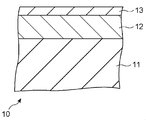
図1に示すように、ICソケット用のコンタクトピンである電気テスト用コンタクト10は、金属材料から成る金属薄板の基材11の打ち抜き加工およびめっき加工により形成されている。そして、図1における電気テスト用コンタクト10の上端がIC端子に接触する接触部10aになり、電気テスト用コンタクト10の下端がテストボードに半田付けされる端子部10bになる。更にその具体的な外形の詳細はICソケットの説明で後述されるが、接触部10aと端子部10bの間に、バネ部10c、支持部10dおよび固定部10eを有する構造になっている。
As shown in FIG. 1, an electrical test contact 10 which is a contact pin for an IC socket is formed by punching and plating a thin metal plate base 11 made of a metal material. The upper end of the electrical test contact 10 in FIG. 1 becomes the contact portion 10a that contacts the IC terminal, and the lower end of the electrical test contact 10 becomes the terminal portion 10b that is soldered to the test board. Further, the details of the specific outer shape will be described later in the description of the IC socket, but the structure has a spring portion 10c, a support portion 10d, and a fixing portion 10e between the contact portion 10a and the terminal portion 10b.
ここで、バネ部10cは、接触部10aの下部に連続し、さらにそこから側方に延在する部分と、当該部分に連続したU字型の湾曲部分とを有することで、ICパッケージ23のリード(後述)との接触に応じて接触部10aに作用する荷重を弾性的に支持する機能を果たす。なお、所望の弾性支持機能を果たすためにバネ部10cの断面寸法および長さ等は適宜定め得るのは勿論である。
Here, the spring part 10c is continuous with the lower part of the contact part 10a, and further has a part extending laterally therefrom, and a U-shaped curved part continuous with the part, so that the IC package 23 It fulfills the function of elastically supporting a load acting on the contact portion 10a in accordance with contact with a lead (described later). Needless to say, the cross-sectional dimension and length of the spring portion 10c can be appropriately determined in order to achieve a desired elastic support function.
支持部10dは、バネ部10cの湾曲部分からバネ部10cの延在部分に平行に延在する。支持部10dの途中からは下方に分岐するように固定部10eが設けられ、さらにその固定部10eに連続して端子部10bが延設されている。なお、支持部10dがバネ部10cの一部として形成されていてもよい。
10 d of support parts are extended in parallel with the extension part of the spring part 10c from the curved part of the spring part 10c. A fixing portion 10e is provided so as to branch downward from the middle of the support portion 10d, and a terminal portion 10b extends continuously from the fixing portion 10e. The support portion 10d may be formed as a part of the spring portion 10c.
本実施形態の電気テスト用コンタクト10では、その全体すなわち上記各部位の全てが打ち抜き加工された金属薄板の基材11表面にNiあるいはNi基合金から成る第1めっき層12と、薄いAuあるいはAu合金から成る第2めっき層13とが順次形成された構造になっている(図2A)。そして、IC端子に接触する接触部10aにおいては、図2Bに示すように、例えばIC端子に対する接点となる上端面から側部にかけての部位にのみ、第2めっき層13の上に更にPdから成る第3めっき層14およびAgから成る第4めっき層15が順次に積層して形成されている。なお、電気テスト用コンタクト10の全体および必要部位の表面に周知の変色防止処理がなされてもよい。
In the electrical test contact 10 of the present embodiment, the first plating layer 12 made of Ni or a Ni-based alloy and the thin Au or Au on the surface of the base 11 of the thin metal plate that has been punched out in its entirety, that is, each of the above-mentioned parts. The second plating layer 13 made of an alloy is sequentially formed (FIG. 2A). And in the contact part 10a which contacts an IC terminal, as shown to FIG. 2B, it consists of Pd further on the 2nd plating layer 13 only in the site | part from the upper end surface used as a contact with respect to an IC terminal to a side part, for example. A third plating layer 14 and a fourth plating layer 15 made of Ag are sequentially stacked. In addition, a known discoloration prevention treatment may be performed on the entire electrical test contact 10 and the surface of a necessary portion.
この電気テスト用コンタクト10の金属めっきに際しては、はじめに基材11の全体に対して、電着により第1めっき層12および第2めっき層13が形成される。そして、その後に接触部10aに関してはさらに、部分的に第3めっき層14および第4めっき層15が形成される。このように、本実施形態に係る電気テスト用コンタクト10では、その製造工程数が余り増えないために製造が簡便なものとなる。
In the metal plating of the electrical test contact 10, first, the first plating layer 12 and the second plating layer 13 are formed on the entire substrate 11 by electrodeposition. Thereafter, the third plating layer 14 and the fourth plating layer 15 are further partially formed with respect to the contact portion 10a. As described above, the electrical test contact 10 according to the present embodiment is easy to manufacture because the number of manufacturing steps does not increase so much.
ここで、上記基材11は、銅(Cu)又はCu合金例えばCu-ベリリウム(Be)系合金、Cu-チタン(Ti)系合金、Cu-Sn系合金(例えば、リン青銅)、Cu-亜鉛(Zn)系合金(例えば、黄銅)等である。
Here, the substrate 11 is made of copper (Cu) or Cu alloy such as Cu-beryllium (Be) alloy, Cu-titanium (Ti) alloy, Cu-Sn alloy (eg phosphor bronze), Cu-zinc. (Zn) based alloys (for example, brass).
第1めっき層12は、基材11とその表層めっき皮膜となる第2めっき層13、第3めっき層14および第4めっき層15の間に生じ易い固相反応を抑制するバリア層であり、Ni、Ni-P合金から成る。その厚さは例えば0.3μm~2μmの範囲で適宜に設定される。
The first plating layer 12 is a barrier layer that suppresses a solid phase reaction that is likely to occur between the base material 11 and the second plating layer 13, the third plating layer 14, and the fourth plating layer 15 that are the surface plating film. Made of Ni, Ni-P alloy. The thickness is appropriately set within a range of 0.3 μm to 2 μm, for example.
第2めっき層13は、例えばフラッシュAuめっきのような電解めっき法により電析されるAuまたはAu基合金から成る。Au基合金としては例えば微量のコバルト(Co)を含むAu-Co合金、Au-Ni合金、Au-Pd合金、Au-Ag合金、Au-Sn合金が挙げられる。第2めっき層13を電解めっき法により形成することにより、第1めっき層12および第3めっき層14との密着性が無電解めっき法を採用した場合より向上する。そして、その厚さは例えば0.05μm~0.30μmの範囲で適宜に設定される。この厚さの範囲は、特許文献1におけるAuあるいはAu基合金から成る表層めっき皮膜の厚さの範囲(0.2~1μm)に比べて大きく低減されたものであり、電気テスト用コンタクト10の低コスト化を容易にする。
The second plating layer 13 is made of Au or an Au-based alloy that is electrodeposited by an electrolytic plating method such as flash Au plating. Examples of the Au-based alloy include an Au—Co alloy containing a trace amount of cobalt (Co), an Au—Ni alloy, an Au—Pd alloy, an Au—Ag alloy, and an Au—Sn alloy. By forming the second plating layer 13 by the electrolytic plating method, the adhesion between the first plating layer 12 and the third plating layer 14 is improved as compared with the case where the electroless plating method is adopted. The thickness is appropriately set in the range of 0.05 μm to 0.30 μm, for example. This thickness range is greatly reduced compared to the thickness range (0.2 to 1 μm) of the surface plating film made of Au or an Au-based alloy in Patent Document 1. Facilitates cost reduction.
ここで、第2めっき層13は、その厚さが0.05μm未満になると、第1めっき層12と第3めっき層14の間での剥がれを生じ易くする。また、その厚さが0.30μm超となると、テストボードのランド等との端子部10bの半田接合の信頼性が低下するようになる。従って、本実施形態のように第2めっき層13の厚さを0.05μm~0.30μmの範囲で設定することは望ましいものとなる。
Here, when the thickness of the second plating layer 13 is less than 0.05 μm, peeling between the first plating layer 12 and the third plating layer 14 is likely to occur. Further, when the thickness exceeds 0.30 μm, the reliability of the solder joint of the terminal portion 10b with the land or the like of the test board is lowered. Therefore, it is desirable to set the thickness of the second plating layer 13 in the range of 0.05 μm to 0.30 μm as in this embodiment.
第3めっき層14は例えば、純PdやPdを基合金としたPd-Ni合金、Pd―In合金の電解めっき、あるいは無電解めっきにより形成される。ここで、Pdめっき層にはその他に不可避不純物が微量に含まれるようになっていてもよい。不可避不純物は上述した電解めっきなどで混入する微量の水素元素、酸素元素、金属元素等である。第3めっき層14の厚さは例えば1μm~2μmの範囲で適宜に設定される。
The third plating layer 14 is formed, for example, by pure Pd or Pd—Ni alloy based on Pd, electrolytic plating of Pd—In alloy, or electroless plating. Here, the Pd plating layer may contain a small amount of other inevitable impurities. The inevitable impurities are a trace amount of hydrogen element, oxygen element, metal element and the like mixed in the above-described electrolytic plating. The thickness of the third plating layer 14 is appropriately set within a range of 1 μm to 2 μm, for example.
第4めっき層15は純AgやAgを基合金としたAg-Sb合金、Ag-Se合金、Ag-Au合金、Ag-Sn合金等の電解めっきあるいは無電解めっきにより形成される。ここで、第4めっき層にはその他に上述したような不可避不純物が微量に含まれるようになっていてもよい。第4めっき層15の厚さは例えば1μm~2μmの範囲で適宜に設定される。第3および第4めっき層は被検体のリードと直接接触するコンタクト頂部にのみ設けるものとしてもよいが、バネ部10cにいたる側部にまで延在させて第2めっき層との積層面積を広くすることで、剥がれの可能性を防ぐことが好ましい。
The fourth plating layer 15 is formed by electrolytic plating or electroless plating of pure Ag or Ag—Sb alloy, Ag—Se alloy, Ag—Au alloy, Ag—Sn alloy, etc. based on Ag. Here, the fourth plating layer may contain a trace amount of inevitable impurities as described above. The thickness of the fourth plating layer 15 is appropriately set within a range of 1 μm to 2 μm, for example. The third and fourth plating layers may be provided only on the contact tops that are in direct contact with the lead of the subject. However, the third and fourth plating layers extend to the side part leading to the spring part 10c to increase the lamination area with the second plating layer. It is preferable to prevent the possibility of peeling.
上記電気テスト用コンタクト10は、図3および図4に示すようなICソケットに必要個数が組込まれて取り付けられる。以下、ICソケットについてその要部を説明する。図3および図4に示すICソケットでは、表面実装型になる例えばQFP(Quad Flat Package)の形態のICパッケージが装着される。ICパッケージのリード表面には錫(Sn)系半田が形成されている。このICソケットは、その外形が概略直方体をなし、ソケット基板21、カバー22および多数の電気テスト用コンタクト10等を備える。
The required number of electrical test contacts 10 are mounted in an IC socket as shown in FIGS. The main part of the IC socket will be described below. In the IC socket shown in FIG. 3 and FIG. 4, an IC package in the form of, for example, QFP (Quad Flat Package) which is a surface mount type is mounted. Tin (Sn) -based solder is formed on the lead surface of the IC package. The IC socket has a substantially rectangular parallelepiped shape, and includes a socket substrate 21, a cover 22, a large number of electrical test contacts 10 and the like.
ソケット基板21は、その中央部にQFPとして組立てられたICパッケージ23が載置される位置決め台24、ソケット基板21に対し着脱自在な台座25等を備える。ICパッケージ23では、多数のガルウィング形リード23aがその4辺から延出する。そして、位置決め台24には、その外周にICパッケージ23の本体を収容するように外周壁24aが設けられている。ここで、多数のガルウィング形リード23aは、外周壁24aを乗り越え、その先端が後述するように電気テスト用コンタクト10の接触部10aに弾性接触できるようになっている。
The socket substrate 21 includes a positioning base 24 on which an IC package 23 assembled as a QFP is placed, a pedestal 25 detachable with respect to the socket substrate 21, and the like. In the IC package 23, a large number of gull-wing leads 23a extend from the four sides. The positioning table 24 is provided with an outer peripheral wall 24a on the outer periphery thereof so as to accommodate the main body of the IC package 23. Here, a large number of gull wing-type leads 23a get over the outer peripheral wall 24a, and their tips can be elastically contacted with the contact portion 10a of the electrical test contact 10 as will be described later.
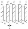
そして、多数の電気テスト用コンタクト10は、その接触部10aが外周壁24aを取り囲むように位置決め台24の外周に沿い配列されている。ここで、電気テスト用コンタクト10は、その固定部10eがソケット基板21の内底面26aから外底面26bに貫通する貫通孔26に嵌合することで固定され、支持部10dがその内底面26aに支持される。また、隣接する電気テスト用コンタクト10同士の接触を防止するために、隣接する電気テスト用コンタクト10間のギャップにはコンタクト分離隔壁27が設けられている。本実施形態においては、コンタクト分離隔壁27は、図3に示されるように、隣接するバネ部10cの湾曲部分が互いに接触しないように配設されている。そして、各バネ部10cはその隔壁間のギャップである溝内で、ICパッケージ23のリード(後述)から加えられる荷重の方向すなわち図3の上下方向に弾性変形するようになる。
A large number of electrical test contacts 10 are arranged along the outer periphery of the positioning table 24 so that the contact portions 10a surround the outer peripheral wall 24a. Here, the electrical test contact 10 is fixed by fitting the fixing portion 10e into the through hole 26 penetrating from the inner bottom surface 26a of the socket substrate 21 to the outer bottom surface 26b, and the support portion 10d is fixed to the inner bottom surface 26a. Supported. Further, in order to prevent contact between adjacent electrical test contacts 10, a contact separation partition 27 is provided in a gap between the adjacent electrical test contacts 10. In the present embodiment, as shown in FIG. 3, the contact separation partition 27 is disposed so that the curved portions of the adjacent spring portions 10c do not contact each other. Each spring portion 10c is elastically deformed in the direction of the load applied from a lead (described later) of the IC package 23, that is, the vertical direction in FIG.
各端子部10bは、テスト基板への実装が行いやすいようソケット基板21の外底面26bから配列が変換され複数列に延出する。ここで、本実施形態では、多数の電気テスト用コンタクト10では、その端子部10bが複数列に二次元配列できるように、その支持部10dから分岐する固定部10eの分岐位置が異なるものが使用されている。そして、この複数列に二次元配列された端子部10bが後述するテストボードの配線端子にそれぞれ半田付けされる。
The arrangement of each terminal portion 10b is converted from the outer bottom surface 26b of the socket substrate 21 so as to be easily mounted on the test substrate, and extends into a plurality of rows. Here, in the present embodiment, a large number of electrical test contacts 10 are used which have different branching positions of the fixing portion 10e branched from the support portion 10d so that the terminal portions 10b can be two-dimensionally arranged in a plurality of rows. Has been. The terminal portions 10b that are two-dimensionally arranged in a plurality of rows are soldered to wiring terminals of a test board, which will be described later.
カバー22は、ソケット基板21の一端に回動自在に枢着され、ソケット基板21を上方向から閉蓋するようになっている。また、カバー22には、その下面適所にICパッケージ23のガルウィング形リード23aを上方向から押える4個のリード押え壁28が設けられている。そして、カバー22の一端領域、好ましくはカバー22の被枢着端と対向する一端の領域にラッチ機構29が設けられ、ソケット基板21の強固な閉蓋、特にリード押え壁28による電気テスト用コンタクト10の接触部10aに対するリード23aの確実な押圧を可能としている。このようにICパッケージ23が図3および図4に示したようなICソケットに装着されて、例えばバーンインテストに供される。
The cover 22 is pivotally attached to one end of the socket substrate 21 so as to close the socket substrate 21 from above. Further, the cover 22 is provided with four lead pressing walls 28 for pressing the gull-wing leads 23a of the IC package 23 from above at appropriate positions on the lower surface thereof. Then, a latch mechanism 29 is provided in one end region of the cover 22, preferably one end region facing the pivoted end of the cover 22, and the electrical test contact by the solid lid of the socket substrate 21, particularly the lead holding wall 28. Thus, the lead 23a can be reliably pressed against the ten contact portions 10a. In this way, the IC package 23 is mounted on the IC socket as shown in FIGS. 3 and 4 and used for, for example, a burn-in test.
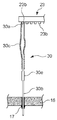
上述したICソケットは、例えばバーンインテストに用いられるテストボードに多数個取り付けられている。ここで、図5に示すように、それぞれのICソケットに組込まれた電気テスト用コンタクト10の端子部10bは、上記テストボード16に例えばフロー半田17により半田付けされている。そして、テストボード16においてそのランド等(図示せず)に接続されている。また、その接触部10aは、リード押え壁28により押圧された対応ガルウィング形リード23aにそれぞれ接触し、バネ部10cにより当該押圧方向(下方)に変位する。
A large number of the above-described IC sockets are attached to a test board used for, for example, a burn-in test. Here, as shown in FIG. 5, the terminal portion 10 b of the electrical test contact 10 incorporated in each IC socket is soldered to the test board 16 by, for example, flow solder 17. The test board 16 is connected to the land or the like (not shown). Further, the contact portion 10a comes into contact with the corresponding gull wing type lead 23a pressed by the lead pressing wall 28, and is displaced in the pressing direction (downward) by the spring portion 10c.
端子部10bの半田付けに使用される半田は、鉛フリーの共晶半田であり、例えば、Sn-亜鉛(Zn)系半田、Sn-Cu系半田、Sn-Ag系半田、Sn-ビスマス(Bi)系半田等が用いられる。ここで、端子部10bはその表面の第1めっき層12がフロー半田17と合金層を形成して、テストボード16のランド等と半田接合することができる。このため、第2めっき層13は、上述したような第1めっき層12のNiの酸化を防止できる程度の薄い厚さで構わない。
The solder used for soldering the terminal portion 10b is lead-free eutectic solder, for example, Sn-zinc (Zn) solder, Sn-Cu solder, Sn-Ag solder, Sn-bismuth (Bi). ) System solder or the like is used. Here, the first plating layer 12 on the surface of the terminal portion 10b forms an alloy layer with the flow solder 17, and can be soldered to a land or the like of the test board 16. For this reason, the second plating layer 13 may be thin enough to prevent the oxidation of Ni of the first plating layer 12 as described above.
上記接触部10aは、上記下方への変位に応じ、バネ部10cが上方に付勢力を作用することにより、ガルウィング形リード23aの表面に形成されている半田めっき層に弾性接触する。このような弾性接触の状態において、例えば125℃程度の高温におけるIC23の検査が行われる。
The contact portion 10a makes elastic contact with the solder plating layer formed on the surface of the gull-wing lead 23a by the biasing force of the spring portion 10c acting upward according to the downward displacement. In such an elastic contact state, the IC 23 is inspected at a high temperature of about 125 ° C., for example.
次に、図6を参照して例えばバーンインテストにおける電気テスト用コンタクト10の作用効果について説明する。図6の(a)に示すように、接触部10aにおける表層めっき皮膜として、上記第2めっき層13を被覆するPdまたはPd基合金から成る第3めっき皮膜14およびAgあるいはAg基合金から成る第4めっき皮膜15がこの順に積層して形成されている。そして、電気テスト用コンタクト10とガルウィング形リード23aとの弾性接触により、図6の(b)に示すように、第4めっき層15がリード23aのSn系半田層18に接触するようになる。
Next, with reference to FIG. 6, for example, the effect of the electrical test contact 10 in the burn-in test will be described. As shown in FIG. 6 (a), as the surface plating film in the contact portion 10a, the third plating film 14 made of Pd or Pd base alloy covering the second plating layer 13 and the first plating made of Ag or Ag base alloy. Four plating films 15 are formed by laminating in this order. Then, due to the elastic contact between the electrical test contact 10 and the gull-wing lead 23a, as shown in FIG. 6B, the fourth plating layer 15 comes into contact with the Sn-based solder layer 18 of the lead 23a.
このような弾性接触の状態において、温度が125℃程度の検査が繰り返し行われると、第2めっき層13、第3めっき層14および第4めっき層15を構成する金属元素中にSn系半田層18が取り込まれるが、めっき層へのSn系半田層18への溶け込みは従来技術の場合に較べ安定的に大きく低減する。これにより電気テスト用コンタクトが長寿命化され、その交換頻度が低減して低コスト化が可能になる。
In such an elastic contact state, when an inspection at a temperature of about 125 ° C. is repeated, the Sn-based solder layer is contained in the metal elements constituting the second plating layer 13, the third plating layer 14, and the fourth plating layer 15. 18 is taken in, but the penetration into the Sn-based solder layer 18 in the plating layer is stably and greatly reduced as compared with the prior art. This prolongs the life of the electrical test contact, reduces the frequency of replacement thereof, and enables cost reduction.
特許文献1に記載されたように表層めっき皮膜がAuあるいはAu合金から成る場合、バーンインテストを繰り返していくと、Au元素が被検体のIC端子のSn系半田層18側に局部的に取り込まれ、半田のSnとの冶金学的な反応が生じる。そして、下地めっき層のNiが局部的に露出するようになり、空気中の酸素と反応して酸化される。このNi酸化物は絶縁体である。このようなNi酸化物の生成により、電気テスト用コンタクトの接触抵抗値が早期に上昇することが生じていた。このために、電気テスト用コンタクトの長寿命化が難しくなっていた。
When the surface plating film is made of Au or an Au alloy as described in Patent Document 1, when the burn-in test is repeated, the Au element is locally taken into the Sn-based solder layer 18 side of the IC terminal of the specimen. A metallurgical reaction of the solder with Sn occurs. And Ni of a base plating layer comes to be exposed locally, it reacts with oxygen in air, and is oxidized. This Ni oxide is an insulator. Due to the generation of such Ni oxide, the contact resistance value of the electrical test contact has risen early. For this reason, it has been difficult to extend the life of electrical test contacts.
これに対して、本実施形態の場合には、図6の(c)に模式的に示したように、逆に、Sn系半田層18中のSn元素が第4めっき層15を通り、第3めっき層14中に吸蔵されるようになる。あるいは、Sn酸化物が還元され、そのSn元素のみが第3めっき層14に吸蔵され、酸素は外部に放散される。そして、バーンインテストが繰り返されていくと第3めっき層14中のSn元素が増えて、第3めっき層14はPdとSnの混合した第3合金めっき層14aになり、その体積増加が生じる。ここで、PdとSnは固溶体あるいは金属間化合物を形成する。
On the other hand, in the case of the present embodiment, as schematically shown in FIG. 6C, conversely, the Sn element in the Sn-based solder layer 18 passes through the fourth plating layer 15, The third plating layer 14 is occluded. Alternatively, the Sn oxide is reduced, only the Sn element is occluded in the third plating layer 14, and oxygen is diffused to the outside. When the burn-in test is repeated, the Sn element in the third plating layer 14 increases, and the third plating layer 14 becomes the third alloy plating layer 14a in which Pd and Sn are mixed, and the volume increases. Here, Pd and Sn form a solid solution or an intermetallic compound.
一方、第4めっき層15はSn元素を拡散させるが第3めっき層14中へのPd元素の拡散を阻止する機能を有する。また、第4めっき層15にSn元素が少し溶け込んだ第3めっき混合層15aになる。しかし、この第4めっき混合層15aはSn系半田層18と接合することはない。また、半田が第4めっき混合層15aの表面に付着することもない。従って、各バーンインテストが終了すると、第4めっき混合層15aとSn系半田層18は相互の剥がれ損傷もなく分離する。
On the other hand, the fourth plating layer 15 has a function of diffusing Sn element but preventing diffusion of Pd element into the third plating layer 14. In addition, the third plating mixed layer 15 a in which the Sn element is slightly dissolved in the fourth plating layer 15 is obtained. However, the fourth plating mixed layer 15 a is not bonded to the Sn-based solder layer 18. Further, the solder does not adhere to the surface of the fourth plating mixed layer 15a. Therefore, when each burn-in test is completed, the fourth plating mixed layer 15a and the Sn-based solder layer 18 are separated from each other without peeling damage.
また、第2めっき層13は第3めっき層14の剥がれを防止する機能を有している。この第2めっき層13が介挿されない場合には、例えばバーンインテストにおける昇降温により生じる第1めっき層12および第3めっき層14の体積膨張および収縮に起因して、それ等の間における剥がれ起こり易い。更に、バーンインテストの繰り返し回数が増えてくると、第3めっき層14の体積増加に起因する剥がれも生じてくるようになる。第2めっき層13は第1めっき層12、第3めっき層14および第3めっき混合層14aに較べて軟質であるので、その応力緩和の作用により上述したような剥がれを防止する。
The second plating layer 13 has a function of preventing the third plating layer 14 from peeling off. When the second plating layer 13 is not inserted, for example, due to the volume expansion and contraction of the first plating layer 12 and the third plating layer 14 caused by the temperature rise and fall in the burn-in test, peeling occurs between them. easy. Furthermore, if the number of repetitions of the burn-in test increases, peeling due to an increase in volume of the third plating layer 14 also occurs. Since the second plating layer 13 is softer than the first plating layer 12, the third plating layer 14, and the third plating mixed layer 14a, the above-described peeling is prevented by the action of stress relaxation.
このようにして、従来技術で生じていたNi酸化物の生成あるいは半田の酸化物(例えば、Sn酸化物)の付着は起こり難くなる。そして、電気テスト用コンタクトの長寿命化が可能になる。それと共に、電気テスト用コンタクトの低コスト化が容易になる。例えば、従来技術を適用した電気テスト用コンタクトでは平均25サイクル程度で接触抵抗値が増大していたICのバーンインテストにおいて、本実施形態の電気テスト用コンタクト10では、100サイクルのバーンインテストの後でも接触抵抗値の上昇は殆ど見られず、その交換サイクルを大幅に伸ばす事が可能となった。
In this way, the generation of Ni oxide or the adhesion of solder oxide (for example, Sn oxide), which has occurred in the prior art, is less likely to occur. In addition, the life of the electrical test contact can be extended. At the same time, it is easy to reduce the cost of the electrical test contact. For example, in the burn-in test of an IC in which the contact resistance value increased in an average of about 25 cycles in an electrical test contact to which the prior art is applied, in the electrical test contact 10 of the present embodiment, even after a 100-cycle burn-in test. Almost no increase in contact resistance was observed, and the exchange cycle could be greatly extended.
また、第3めっき層14および第4めっき層15は、電気テスト用コンタクト10に部分的に、すなわち接触部10a上の部分にのみ、電着により積層され、バネ部10cには形成されない。このため、電気テスト用コンタクト10のコンタクト分離隔壁27に対する充分なクリアランスを確保し易くなる。そして、バネ部10cの上下方向への弾性変形が充分に確保され、接触部10aのIC端子との必要な弾性接触が保障される。これについて、図7を参照した説明を加える。図7は、図3に示すコンタクト分離隔壁の上方からの斜め下方の拡大図である。
Also, the third plating layer 14 and the fourth plating layer 15 are laminated by electrodeposition partially on the electrical test contact 10, that is, only on the contact portion 10a, and are not formed on the spring portion 10c. For this reason, it becomes easy to ensure a sufficient clearance for the contact separating partition 27 of the electrical test contact 10. And the elastic deformation to the up-down direction of the spring part 10c is fully ensured, and the required elastic contact with the IC terminal of the contact part 10a is ensured. This will be described with reference to FIG. FIG. 7 is an enlarged view obliquely downward from above the contact separation partition wall shown in FIG.
図7に示すように、多数の電気テスト用コンタクト10は例えば各バネ部10cがコンタクト分離隔壁27により隔離されて、互いに接触しないようにしなければならない。一方、上記バーンインテストにおける電気テスト用コンタクト10の効果は、第3めっき層14および第4めっき層15を厚くするほど顕著になる。本実施形態においては、バネ部10cには第3めっき層14および第4めっき層15が形成されないため、第3めっき層14および第4めっき層15を好ましい厚さに形成しつつも、コンタクト分離隔壁27との間のクリアランスLは確保できるようになる。このために、IC端子の多ピン化あるいは狭ピッチ化に対応して、多数の電気テスト用コンタクト10を近接させて配列することが可能になる。
As shown in FIG. 7, a large number of electrical test contacts 10 must be separated from each other by, for example, the spring portions 10 c by the contact separation partition 27 so as not to contact each other. On the other hand, the effect of the electrical test contact 10 in the burn-in test becomes more prominent as the third plating layer 14 and the fourth plating layer 15 become thicker. In the present embodiment, since the third plating layer 14 and the fourth plating layer 15 are not formed on the spring portion 10c, contact separation is performed while the third plating layer 14 and the fourth plating layer 15 are formed to have a preferable thickness. The clearance L between the partition walls 27 can be secured. For this reason, it becomes possible to arrange a large number of electrical test contacts 10 close to each other in accordance with the increase in the number of pins of IC terminals or the decrease in pitch.
また、上記第3めっき層14および第4めっき層15は電気テスト用コンタクト10に部分的に電着され、端子部10bには形成されない。そして、上述したように端子部10bは、主に基材11表面の第1めっき層12と第2めっき層13がフロー半田17と合金層を形成してテストボード16のスルーホール等と半田接合している。このために、上記バーンインテストにおいてその接合強度の低下は全く生じない。
In addition, the third plating layer 14 and the fourth plating layer 15 are partially electrodeposited on the electrical test contact 10 and are not formed on the terminal portion 10b. As described above, the terminal portion 10b is mainly formed by soldering the first plating layer 12 and the second plating layer 13 on the surface of the base material 11 to form a flow solder 17 and an alloy layer to a through hole or the like of the test board 16. is doing. For this reason, in the burn-in test, no decrease in the bonding strength occurs.
これに対して、第3めっき層14および第4めっき層15の電着が部分的でなく、端子部10bに形成されると、テストボード16のランド等との半田接合は、フロー半田17とPdを含む第3めっき層14あるいはAgを含む第4めっき層15との合金層によることになる。しかし、この場合には、その接合強度がNiを含む第1めっき層12およびAuを含む第2めっき層13との合金層による半田接合の場合に比べ低下する傾向がある(なお、上記バーンインテストを実施しない場合でも、その接合強度が低くなる傾向がある)。また、この強度の低下は上記バーンインテストを行う場合において顕著となる。これは、バーンインテスト時の温度環境下での経時変化により、基材11が含むCuが第1めっき層12および第2めっき層13を越えてPdとSnとの接合部へと拡散し、CuとSnとの金属間化合物が生成されるためと考えられる。
On the other hand, if the electrodeposition of the third plating layer 14 and the fourth plating layer 15 is not partial and is formed on the terminal portion 10b, the solder bonding with the land of the test board 16 is performed with the flow solder 17 and the like. This is due to the alloy layer with the third plating layer 14 containing Pd or the fourth plating layer 15 containing Ag. However, in this case, the bonding strength tends to be lower than in the case of solder bonding using an alloy layer with the first plating layer 12 containing Ni and the second plating layer 13 containing Au (the burn-in test). Even if not, the bonding strength tends to be low). Further, this decrease in strength becomes significant when the burn-in test is performed. This is because Cu contained in the base material 11 diffuses over the first plating layer 12 and the second plating layer 13 to the junction between Pd and Sn due to the change over time in the temperature environment during the burn-in test. This is probably because an intermetallic compound of Sn and Sn is generated.
なお、上記電気テスト用コンタクト10では、第3めっき層14および第4めっき層15が図1あるいは図5に示したように接触部10aの側部を含めた接触部10aの上方の領域に部分的に形成されるように説明しているが、本発明はこれに限定されるものでない。第3めっき層14および第4めっき層15は、接触部10aの上端面のみに形成されていても構わない。すなわち、第3めっき層14および第4めっき層15が形成される領域は接触部10aにおいてIC端子に実質的に接触する部分に限局されていてもよい。
In the electrical test contact 10, the third plating layer 14 and the fourth plating layer 15 are partially formed in the region above the contact portion 10a including the side portion of the contact portion 10a as shown in FIG. 1 or FIG. However, the present invention is not limited to this. The third plating layer 14 and the fourth plating layer 15 may be formed only on the upper end surface of the contact portion 10a. That is, the region where the third plating layer 14 and the fourth plating layer 15 are formed may be limited to a portion of the contact portion 10a that substantially contacts the IC terminal.
(他の実施形態)
次に、ICソケットに取り付けられる電気テスト用コンタクトの他の実施形態について図8を参照して説明する。この電気テスト用コンタクト30は上下方向に略直線状になったコンタクトピンである。ここで、図8におけるその上端がIC端子に接触する接触部30aになり、その下端がテストボード16にフロー半田17により半田付けされる端子部30bになる。そして、上記接触部30aと端子部30bの間に、コンタクト30の長手方向に対して横方向に弾性変形するバネ部30cと、ICソケットに支持され固定される支持部30eが形成される。この場合のICソケットは、図3および図4で説明した構成を、本実施形態に係る電気テスト用コンタクト30に適合するように変更すればよい。接触部30aを一端としたバネ部30cは2枚の細長い弾性接片の基材から成り、その他端が靱性のある針状の支持部30eに一体接合している。そして、針状の支持部30eを基端としてその先端が端子部30bになっている。なお、IC端子と接触部30aとの接触に応じてバネ部30cが弾性変形する方向、すなわち2枚の細長い弾性接片が開く方向は、隣接する電気テスト用コンタクト30のバネ部30cの接触が生じないように定められる。
(Other embodiments)
Next, another embodiment of the electrical test contact attached to the IC socket will be described with reference to FIG. The electrical test contact 30 is a contact pin that is substantially linear in the vertical direction. Here, the upper end in FIG. 8 becomes the contact portion 30 a that contacts the IC terminal, and the lower end becomes the terminal portion 30 b that is soldered to the test board 16 by the flow solder 17. Between the contact portion 30a and the terminal portion 30b, a spring portion 30c that is elastically deformed in the lateral direction with respect to the longitudinal direction of the contact 30 and a support portion 30e that is supported and fixed by the IC socket are formed. The IC socket in this case may be modified so that the configuration described with reference to FIGS. 3 and 4 is adapted to the electrical test contact 30 according to the present embodiment. The spring portion 30c with one end of the contact portion 30a is made of a base material of two elongated elastic contact pieces, and the other end is integrally joined to a tough needle-like support portion 30e. And the needle-shaped support part 30e is made into the base end, and the front-end | tip is the terminal part 30b. In the direction in which the spring portion 30c is elastically deformed in response to the contact between the IC terminal and the contact portion 30a, that is, the direction in which the two elongated elastic contact pieces are opened, the contact of the spring portion 30c of the adjacent electrical test contact 30 is It is determined not to occur.
この電気テスト用コンタクト30では、電気テスト用コンタクト10で説明したのと同じように、上述した各部位の全体が基材11表面にNiあるいはNi基合金から成る第1めっき層12と、薄いAuあるいはAu基合金から成る第2めっき層13が順次に形成された構造になっている。そして、従来技術で説明したBGAの半田ボール23bに接触する接触部30aにおいて選択的に、上記第2めっき層13に更にPdまたはPd基合金から成る第3めっき層14およびAgあるいはAg基合金から成る第4めっき層15が順次に積層して形成されている。更に、周知の変色防止処理がなされてもよい。
In the electrical test contact 30, as described in the electrical test contact 10, the entire portion described above is formed on the surface of the substrate 11 with the first plating layer 12 made of Ni or a Ni-based alloy, and the thin Au Alternatively, the second plating layer 13 made of an Au base alloy is sequentially formed. Then, in the contact portion 30a that contacts the BGA solder ball 23b described in the prior art, the second plating layer 13 is further made of a third plating layer 14 made of Pd or a Pd-based alloy and Ag or an Ag-based alloy. The fourth plating layer 15 is formed by sequentially laminating. Furthermore, a known discoloration prevention process may be performed.
次に、電気テスト用コンタクトのさらに他の2実施形態について図9Aおよび図9Bを参照した説明を加える。これらの例では、電気テスト用コンタクト40,50はICソケットに取り付けられるコンタクトピンであるが、テストボード16に半田付けされない。
Next, description will be made with reference to FIGS. 9A and 9B for two other embodiments of the electrical test contact. In these examples, the electrical test contacts 40 and 50 are contact pins attached to the IC socket, but are not soldered to the test board 16.
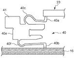
図9Aに示す電気テスト用コンタクト40では、薄板の打ち抜き加工により形成された基材41でなり、同図におけるその上端がIC端子に弾性接触する第1接触部40aになり、その下端がテストボード16のランド等に弾性接触する第2接触部40bになる。そして、第1接触部40aは第1バネ部40cを通して固定部40eに連結され、第2接触部40bは第2バネ部40fを通して固定部40eに連結される。ここで、電気テスト用コンタクト40は取り付けられるICソケット内の所定の位置に固定部40eで固定されるようになる。この場合のICソケットについても、図3および図4で説明した構成を、本実施形態に係る電気テスト用コンタクト40に適合するように変更すればよい。
The electrical test contact 40 shown in FIG. 9A is made of a base material 41 formed by punching a thin plate, and its upper end in FIG. 9A is a first contact portion 40a that elastically contacts the IC terminal, and its lower end is a test board. It becomes the 2nd contact part 40b which elastically contacts 16 lands. The first contact part 40a is connected to the fixed part 40e through the first spring part 40c, and the second contact part 40b is connected to the fixed part 40e through the second spring part 40f. Here, the electrical test contact 40 is fixed at a predetermined position in the IC socket to be attached by the fixing portion 40e. For the IC socket in this case, the configuration described with reference to FIGS. 3 and 4 may be changed so as to be compatible with the electrical test contact 40 according to the present embodiment.
電気テスト用コンタクト40では、電気テスト用コンタクト10で説明したのと同じように、上述した各部位の全体が基材11の表面にNiあるいはNi基合金から成る第1めっき層12と、薄いAuあるいはAu合金から成る第2めっき層13が順次施された構造になっている。そして、例えばベアチップであるIC23の半田バンプ(図示せず)に接触する第1接触部40aのみに、例えば図中の点線より上方の部分となる上端に、上記第2めっき層13の上層として更にPdまたはPd基合金から成る第3めっき層14およびAgあるいはAg基合金から成る第4めっき層15が順次に積層して形成されている。更に、周知の変色防止処理がなされてもよい。
In the electrical test contact 40, as described in the electrical test contact 10, the entire portion described above is formed on the surface of the base 11 with the first plating layer 12 made of Ni or a Ni-based alloy, and the thin Au Alternatively, the second plating layer 13 made of an Au alloy is sequentially applied. Further, for example, only on the first contact portion 40a that contacts a solder bump (not shown) of the IC 23 that is a bare chip, for example, on the upper end that is a portion above the dotted line in the drawing, as an upper layer of the second plating layer 13 A third plating layer 14 made of Pd or a Pd-based alloy and a fourth plating layer 15 made of Ag or an Ag-based alloy are sequentially laminated. Furthermore, a known discoloration prevention process may be performed.
一方、テストボード16のランド等に接触する第2接触部40bにおいて、例えば図中の点線より下方の部分となる下端に選択的に、第2めっき層13の上に更にAuあるいはAu基合金のめっき層が追加形成される。そして、この領域では第2めっき層13の厚さが例えば0,2μm~1μm程度とされる。
On the other hand, in the second contact portion 40b that contacts the land of the test board 16, for example, selectively at the lower end that is a portion below the dotted line in the drawing, Au or an Au-based alloy is further formed on the second plating layer 13. An additional plating layer is formed. In this region, the thickness of the second plating layer 13 is, for example, about 0.2 μm to 1 μm.
図9Bに示す電気テスト用コンタクト50は図の上下方向に直線状に延在するコンタクトピンである。そして、図におけるその上端がIC端子に接触する第1接触部50aになる第1プランジャ50bと、下端がテストボードのランド等に接触する第2接触部50cになる第2プランジャ50dとがバレル50e内で互いに係合する。ここで、これ等の第1プランジャ50bおよび第2プランジャ50dは、バレル50e内のコイルバネ(図示せず)を介して、バレル50eから突出する方向、すなわち上方および下方にそれぞれ付勢される。この電気テスト用コンタクト50は、図3および図4で説明した構成を本実施形態に適合するように変更したICソケットに取り付けられる。なお、これ等のプランジャは例えば金属棒の切削加工等により形成された基材でなる。
The electrical test contact 50 shown in FIG. 9B is a contact pin extending linearly in the vertical direction of the figure. In the drawing, a barrel 50e includes a first plunger 50b serving as a first contact portion 50a whose upper end contacts the IC terminal and a second plunger 50d serving as a second contact portion 50c whose lower end contacts a land of the test board. Within each other. Here, the first plunger 50b and the second plunger 50d are biased in a direction protruding from the barrel 50e, that is, upward and downward, via a coil spring (not shown) in the barrel 50e. The electrical test contact 50 is attached to an IC socket in which the configuration described with reference to FIGS. 3 and 4 is changed to be compatible with the present embodiment. These plungers are made of a base material formed by cutting a metal rod, for example.
電気テスト用コンタクト50では、電気テスト用コンタクト10で説明したのと同じように、上述した各部位の全体が基材11の表面にNiあるいはNi基合金から成る第1めっき層12と、薄いAuあるいはAu合金から成る第2めっき層13が順次施された構造になる。そして、CSPに組立てられたIC23のBGAの半田ボール23bに接触する第1接触部50aにおいて、例えば図中の点線から上方の部分に選択的に、上記第2めっき層13の上層として更にPdまたはPd基合金から成る第3めっき層14およびAgあるいはAg基合金から成る第4めっき層15が順次に積層して形成される。更に、周知の変色防止処理がなされてもよい。ここで、第1接触部50aの先端は、半田ボール23bとの接触が良好になるように略90度の角度をなす三角溝状に形成されるとよい。
In the electrical test contact 50, as described in the electrical test contact 10, the entire portion described above is formed on the surface of the base 11 with the first plating layer 12 made of Ni or a Ni-based alloy, and the thin Au Or it becomes the structure where the 2nd plating layer 13 which consists of Au alloy was given one by one. Then, in the first contact portion 50a that contacts the BGA solder ball 23b of the IC 23 assembled in the CSP, for example, selectively on the upper part from the dotted line in the drawing, Pd or further as the upper layer of the second plating layer 13 A third plating layer 14 made of a Pd-based alloy and a fourth plating layer 15 made of Ag or an Ag-based alloy are sequentially laminated. Furthermore, a known discoloration prevention process may be performed. Here, the tip of the first contact portion 50a is preferably formed in a triangular groove shape having an angle of approximately 90 degrees so that the contact with the solder ball 23b is good.
これに対して、テストボード16のランド等に接触する第2接触部50cにおいて、例えば点線より下方の部分となる下端に選択的に、第2めっき層13の上に更にAuあるいはAu基合金のめっき層が追加形成される。そして、この領域では第2めっき層13の厚さが例えば0,2μm~1μm程度とされ。なお、この電気テスト用コンタクト50の場合、バレル50eの表面にはめっき層を形成せず、基材11が剥き出しの構造になっていてもよい。
On the other hand, in the second contact part 50c that contacts the land of the test board 16 or the like, for example, selectively at the lower end that is a part below the dotted line, Au or an Au-based alloy is further formed on the second plating layer 13. An additional plating layer is formed. In this region, the thickness of the second plating layer 13 is, for example, about 0.2 μm to 1 μm. In the case of the electrical test contact 50, the base layer 11 may be exposed without forming a plating layer on the surface of the barrel 50e.
(その他)
上述した各実施形態に係る電気テスト用コンタクトは、ICソケットに取り付けられるコンタクトピンの形態を有するが、その他に、背景技術の項で説明したコンタクトプローブの形態を有していてもよい。このような電気テスト用コンタクトは前述のBGA、CSPの他、ウエーハレベルCSPのいわゆるウエーハレベルバーンインでも好適に使用される。その基本的な構造では、コンタクトプローブの一端となる接触子がウエーハに配列されている被検体のICチップの例えばSn合金系半田から成る半田バンプに弾性接触するように構成する。そして、コンタクトプローブの基端が例えばジャンパー線等を介しプローバのプローブカードのランド等と電気接続するようにする。
(Other)
The electrical test contacts according to the above-described embodiments have the form of contact pins attached to the IC socket, but may have the form of contact probes described in the background art section. Such an electrical test contact is suitably used in the so-called wafer level burn-in of a wafer level CSP in addition to the BGA and CSP described above. In the basic structure, the contact which is one end of the contact probe is configured to elastically contact a solder bump made of, for example, Sn alloy solder of the IC chip of the subject arranged on the wafer. Then, the base end of the contact probe is electrically connected to, for example, a land of a prober probe card via a jumper wire or the like.
この場合も、コンタクトプローブの各部位の全体が図2Aで説明したように、金属材料から成る基材11の表面にNiあるいはNi基合金から成る第1めっき層12と、薄いAuあるいはAu合金から成る第2めっき層13が順次施された構造になる。そして、ICチップの半田バンプに接触する接触子において選択的に、上記第2めっき層13の上に更にPdまたはPd基合金から成る第3めっき層14およびAgあるいはAg基合金から成る第4めっき層15が順次に積層して形成されている。更に、周知の変色防止処理がなされてもよい。一方、コンタクトプローブの基端側は鉛フリー半田により例えばジャンパー線と半田接合する。
Also in this case, as described in FIG. 2A, the entire portion of the contact probe is made of the first plating layer 12 made of Ni or Ni-based alloy and the thin Au or Au alloy on the surface of the base material 11 made of a metal material. The second plating layer 13 is sequentially applied. Then, a contact that contacts the solder bumps of the IC chip is selectively provided on the second plating layer 13 with a third plating layer 14 made of Pd or a Pd-based alloy and a fourth plating made of Ag or an Ag-based alloy. The layers 15 are formed by sequentially laminating. Furthermore, a known discoloration prevention process may be performed. On the other hand, the base end side of the contact probe is soldered to, for example, a jumper wire by lead-free solder.
上記電気テスト用コンタクトにおいて、IC端子に接触する接触部(10a,30a,40a,50a)あるいは接触子、テストボード側の端子部(10b,30b)あるいは第2接触部(40b,50c)または基端を除く電気テスト用コンタクトの部位は、基材11の表面に第1めっき層12のみが形成される形態であってもよい。この場合、バーンインテストにおいて、当該部位上のNiから成る第1めっき層12はその表面が少し酸化されるようになる。そして、電気テスト用コンタクトにおける当該部位のバネ弾性特性の経時変化が生じ得るが、基材11の金属材料を適宜に選択することによりこのような問題は回避できる。
In the electrical test contact, the contact portion (10a, 30a, 40a, 50a) or contact that contacts the IC terminal, the test board side terminal portion (10b, 30b), the second contact portion (40b, 50c) or the base The part of the contact for electrical test excluding the end may be in a form in which only the first plating layer 12 is formed on the surface of the substrate 11. In this case, in the burn-in test, the surface of the first plating layer 12 made of Ni on the portion is slightly oxidized. And although the time-dependent change of the spring elastic characteristic of the said site | part in an electrical test contact may arise, such a problem can be avoided by selecting the metal material of the base material 11 suitably.
本実施形態の電気テスト用コンタクトは、例えばバーンインテスト、加速ストレス試験のような高温環境下におけるICの通電検査において、その安定した長寿命化を可能にする。そして、通電検査のための被検体との間における多数回の繰り返し接触および分離が安定して高い信頼性のもとに可能となる。
The electrical test contact of the present embodiment enables a stable and long life in an IC energization test under a high temperature environment such as a burn-in test and an accelerated stress test. In addition, a large number of repeated contacts and separations with the subject for the current test can be stably performed with high reliability.
また、電気テスト用コンタクトの接触部に部分的にPdから成るめっき層とAgあるいはAg基合金から成るめっき層を積層して形成することにより、ICソケット内への多数の電気テスト用コンタクトの配列が高い信頼性のもとに可能となる。このようにして、IC端子の多ピン化あるいは狭ピッチ化への対応が容易になる。
In addition, by arranging a plating layer made of Pd and a plating layer made of Ag or an Ag-based alloy partially on the contact portion of the electrical test contact, an array of a large number of electrical test contacts in the IC socket is formed. Is possible with high reliability. In this way, it becomes easy to cope with the increase in the number of pins of IC terminals or the reduction in pitch.
そして、上述した長寿命化により、電気テスト用コンタクト、その取り付けICソケットあるいはプローブヘッド等の交換頻度が低減する。また、電気テスト用コンタクトへの高価なAu金属の使用量は大幅に減少する。更に、本実施形態の電気テスト用コンタクトの製法は簡便になる。このようにして、電気テスト用コンタクトの低コスト化が容易になる。これは、IC端子の多ピン化あるいは狭ピッチ化において顕著になる。
And, by extending the life as described above, the frequency of replacement of the electrical test contact, its mounting IC socket, probe head, etc. is reduced. Also, the amount of expensive Au metal used for electrical test contacts is greatly reduced. Furthermore, the manufacturing method of the electrical test contact of this embodiment is simplified. In this way, cost reduction of the electrical test contact is facilitated. This becomes prominent when the number of IC terminals is increased or the pitch is reduced.
以上、本発明の好適な実施形態について説明したが、上述した実施形態は本発明を限定するものでない。当業者にあっては、具体的な実施態様において本発明の技術思想および技術範囲から逸脱せずに種々の変形あるいは変更を加えることが可能である。
The preferred embodiments of the present invention have been described above, but the above-described embodiments do not limit the present invention. Those skilled in the art can make various modifications or changes in specific embodiments without departing from the technical idea and scope of the present invention.
本発明は、例えばウエーハレベルバーンインで用いられる例えばスプリングプローブのような電気テスト用コンタクトであっても同様に適用される。
The present invention is similarly applied to an electrical test contact such as a spring probe used in wafer level burn-in, for example.
また、上記電気テスト用コンタクトは、高温環境下の通電検査に限らず、例えば室温下でのICのような電子部品の通電検査にも有用になる。
Further, the electrical test contact is useful not only for energization inspection in a high temperature environment but also for energization inspection of electronic components such as ICs at room temperature.